US10649589B2 - Touch apparatus, electronic device and preparing method - Google Patents
Touch apparatus, electronic device and preparing method Download PDFInfo
- Publication number
- US10649589B2 US10649589B2 US15/622,022 US201715622022A US10649589B2 US 10649589 B2 US10649589 B2 US 10649589B2 US 201715622022 A US201715622022 A US 201715622022A US 10649589 B2 US10649589 B2 US 10649589B2
- Authority
- US
- United States
- Prior art keywords
- touch sensor
- substrate
- touch
- display region
- projection
- Prior art date
- Legal status (The legal status is an assumption and is not a legal conclusion. Google has not performed a legal analysis and makes no representation as to the accuracy of the status listed.)
- Active
Links
- 238000000034 method Methods 0.000 title abstract description 34
- 239000000758 substrate Substances 0.000 claims abstract description 165
- 238000001514 detection method Methods 0.000 claims description 33
- 229910052751 metal Inorganic materials 0.000 claims description 5
- 239000002184 metal Substances 0.000 claims description 5
- 239000003292 glue Substances 0.000 claims description 3
- 239000000463 material Substances 0.000 claims description 2
- 239000010410 layer Substances 0.000 description 51
- 238000010586 diagram Methods 0.000 description 43
- 238000002834 transmittance Methods 0.000 description 7
- QNRATNLHPGXHMA-XZHTYLCXSA-N (r)-(6-ethoxyquinolin-4-yl)-[(2s,4s,5r)-5-ethyl-1-azabicyclo[2.2.2]octan-2-yl]methanol;hydrochloride Chemical compound Cl.C([C@H]([C@H](C1)CC)C2)CN1[C@@H]2[C@H](O)C1=CC=NC2=CC=C(OCC)C=C21 QNRATNLHPGXHMA-XZHTYLCXSA-N 0.000 description 4
- 238000005452 bending Methods 0.000 description 4
- 238000005538 encapsulation Methods 0.000 description 4
- 238000009413 insulation Methods 0.000 description 4
- 238000010292 electrical insulation Methods 0.000 description 3
- 238000005516 engineering process Methods 0.000 description 3
- 229920000139 polyethylene terephthalate Polymers 0.000 description 3
- 239000005020 polyethylene terephthalate Substances 0.000 description 3
- 229920000089 Cyclic olefin copolymer Polymers 0.000 description 2
- 239000004713 Cyclic olefin copolymer Substances 0.000 description 2
- 230000015572 biosynthetic process Effects 0.000 description 2
- 238000011161 development Methods 0.000 description 2
- 239000002346 layers by function Substances 0.000 description 2
- 239000004973 liquid crystal related substance Substances 0.000 description 2
- 238000012544 monitoring process Methods 0.000 description 2
- 230000009286 beneficial effect Effects 0.000 description 1
- 239000004020 conductor Substances 0.000 description 1
- 238000013461 design Methods 0.000 description 1
- 239000010408 film Substances 0.000 description 1
- AMGQUBHHOARCQH-UHFFFAOYSA-N indium;oxotin Chemical class [In].[Sn]=O AMGQUBHHOARCQH-UHFFFAOYSA-N 0.000 description 1
- 238000004519 manufacturing process Methods 0.000 description 1
- 238000012986 modification Methods 0.000 description 1
- 230000004048 modification Effects 0.000 description 1
- 230000003287 optical effect Effects 0.000 description 1
- -1 polyethylene terephthalate Polymers 0.000 description 1
- 229920006254 polymer film Polymers 0.000 description 1
- 230000000750 progressive effect Effects 0.000 description 1
- 238000012360 testing method Methods 0.000 description 1
- 239000010409 thin film Substances 0.000 description 1
Images


Classifications
-
- G—PHYSICS
- G06—COMPUTING; CALCULATING OR COUNTING
- G06F—ELECTRIC DIGITAL DATA PROCESSING
- G06F3/00—Input arrangements for transferring data to be processed into a form capable of being handled by the computer; Output arrangements for transferring data from processing unit to output unit, e.g. interface arrangements
- G06F3/01—Input arrangements or combined input and output arrangements for interaction between user and computer
- G06F3/03—Arrangements for converting the position or the displacement of a member into a coded form
- G06F3/041—Digitisers, e.g. for touch screens or touch pads, characterised by the transducing means
- G06F3/044—Digitisers, e.g. for touch screens or touch pads, characterised by the transducing means by capacitive means
-
- G—PHYSICS
- G06—COMPUTING; CALCULATING OR COUNTING
- G06F—ELECTRIC DIGITAL DATA PROCESSING
- G06F1/00—Details not covered by groups G06F3/00 - G06F13/00 and G06F21/00
- G06F1/16—Constructional details or arrangements
- G06F1/1613—Constructional details or arrangements for portable computers
- G06F1/1633—Constructional details or arrangements of portable computers not specific to the type of enclosures covered by groups G06F1/1615 - G06F1/1626
- G06F1/1637—Details related to the display arrangement, including those related to the mounting of the display in the housing
- G06F1/1652—Details related to the display arrangement, including those related to the mounting of the display in the housing the display being flexible, e.g. mimicking a sheet of paper, or rollable
-
- G—PHYSICS
- G06—COMPUTING; CALCULATING OR COUNTING
- G06F—ELECTRIC DIGITAL DATA PROCESSING
- G06F3/00—Input arrangements for transferring data to be processed into a form capable of being handled by the computer; Output arrangements for transferring data from processing unit to output unit, e.g. interface arrangements
- G06F3/01—Input arrangements or combined input and output arrangements for interaction between user and computer
- G06F3/03—Arrangements for converting the position or the displacement of a member into a coded form
- G06F3/041—Digitisers, e.g. for touch screens or touch pads, characterised by the transducing means
- G06F3/0412—Digitisers structurally integrated in a display
-
- G—PHYSICS
- G06—COMPUTING; CALCULATING OR COUNTING
- G06F—ELECTRIC DIGITAL DATA PROCESSING
- G06F3/00—Input arrangements for transferring data to be processed into a form capable of being handled by the computer; Output arrangements for transferring data from processing unit to output unit, e.g. interface arrangements
- G06F3/01—Input arrangements or combined input and output arrangements for interaction between user and computer
- G06F3/03—Arrangements for converting the position or the displacement of a member into a coded form
- G06F3/041—Digitisers, e.g. for touch screens or touch pads, characterised by the transducing means
- G06F3/0416—Control or interface arrangements specially adapted for digitisers
- G06F3/04164—Connections between sensors and controllers, e.g. routing lines between electrodes and connection pads
-
- G—PHYSICS
- G06—COMPUTING; CALCULATING OR COUNTING
- G06F—ELECTRIC DIGITAL DATA PROCESSING
- G06F3/00—Input arrangements for transferring data to be processed into a form capable of being handled by the computer; Output arrangements for transferring data from processing unit to output unit, e.g. interface arrangements
- G06F3/01—Input arrangements or combined input and output arrangements for interaction between user and computer
- G06F3/03—Arrangements for converting the position or the displacement of a member into a coded form
- G06F3/041—Digitisers, e.g. for touch screens or touch pads, characterised by the transducing means
- G06F3/044—Digitisers, e.g. for touch screens or touch pads, characterised by the transducing means by capacitive means
- G06F3/0443—Digitisers, e.g. for touch screens or touch pads, characterised by the transducing means by capacitive means using a single layer of sensing electrodes
-
- G—PHYSICS
- G06—COMPUTING; CALCULATING OR COUNTING
- G06F—ELECTRIC DIGITAL DATA PROCESSING
- G06F3/00—Input arrangements for transferring data to be processed into a form capable of being handled by the computer; Output arrangements for transferring data from processing unit to output unit, e.g. interface arrangements
- G06F3/01—Input arrangements or combined input and output arrangements for interaction between user and computer
- G06F3/03—Arrangements for converting the position or the displacement of a member into a coded form
- G06F3/041—Digitisers, e.g. for touch screens or touch pads, characterised by the transducing means
- G06F3/044—Digitisers, e.g. for touch screens or touch pads, characterised by the transducing means by capacitive means
- G06F3/0445—Digitisers, e.g. for touch screens or touch pads, characterised by the transducing means by capacitive means using two or more layers of sensing electrodes, e.g. using two layers of electrodes separated by a dielectric layer
-
- G—PHYSICS
- G06—COMPUTING; CALCULATING OR COUNTING
- G06F—ELECTRIC DIGITAL DATA PROCESSING
- G06F3/00—Input arrangements for transferring data to be processed into a form capable of being handled by the computer; Output arrangements for transferring data from processing unit to output unit, e.g. interface arrangements
- G06F3/01—Input arrangements or combined input and output arrangements for interaction between user and computer
- G06F3/03—Arrangements for converting the position or the displacement of a member into a coded form
- G06F3/041—Digitisers, e.g. for touch screens or touch pads, characterised by the transducing means
- G06F3/044—Digitisers, e.g. for touch screens or touch pads, characterised by the transducing means by capacitive means
- G06F3/0446—Digitisers, e.g. for touch screens or touch pads, characterised by the transducing means by capacitive means using a grid-like structure of electrodes in at least two directions, e.g. using row and column electrodes
-
- H—ELECTRICITY
- H05—ELECTRIC TECHNIQUES NOT OTHERWISE PROVIDED FOR
- H05K—PRINTED CIRCUITS; CASINGS OR CONSTRUCTIONAL DETAILS OF ELECTRIC APPARATUS; MANUFACTURE OF ASSEMBLAGES OF ELECTRICAL COMPONENTS
- H05K1/00—Printed circuits
- H05K1/02—Details
- H05K1/0277—Bendability or stretchability details
- H05K1/028—Bending or folding regions of flexible printed circuits
-
- G—PHYSICS
- G06—COMPUTING; CALCULATING OR COUNTING
- G06F—ELECTRIC DIGITAL DATA PROCESSING
- G06F2203/00—Indexing scheme relating to G06F3/00 - G06F3/048
- G06F2203/041—Indexing scheme relating to G06F3/041 - G06F3/045
- G06F2203/04102—Flexible digitiser, i.e. constructional details for allowing the whole digitising part of a device to be flexed or rolled like a sheet of paper
-
- G—PHYSICS
- G06—COMPUTING; CALCULATING OR COUNTING
- G06F—ELECTRIC DIGITAL DATA PROCESSING
- G06F2203/00—Indexing scheme relating to G06F3/00 - G06F3/048
- G06F2203/041—Indexing scheme relating to G06F3/041 - G06F3/045
- G06F2203/04103—Manufacturing, i.e. details related to manufacturing processes specially suited for touch sensitive devices
Definitions
- the present disclosure relates to the technical field of electronic device, and in particular to a touch apparatus, an electronic device and a preparing method.
- a touch sensor is a main component of the electronic device to achieve the touch function.
- a bendable touch sensor is applicable to more application environments because of the flexibility and portability. Therefore, the bendable touch sensor is a development direction of the touch sensor.
- touch electrodes in the touch sensor are made of metal or Indium Tin Oxides (ITO), the touch electrodes tend to break up when the touch sensor is bent, which results in a low lifespan of the touch sensor.
- ITO Indium Tin Oxides
- the touch apparatus includes two touch sensors to facilitate bending and improve a lifespan of the touch sensor.
- the touch apparatus includes a substrate, a cover plate, a first touch sensor, and a second touch sensor.
- the substrate and the cover plate are arranged opposite to each other.
- the substrate includes a display region, and the display region includes a first display region and a second display region arranged in a first direction.
- the first touch sensor is arranged on the side of the cover plate towards the substrate.
- the second touch sensor is arranged on the side of the substrate towards the cover plate.
- the second touch sensor is arranged in a different layer from the first touch sensor.
- the first direction is parallel to the substrate.
- the first touch sensor has a first projection on the substrate in a second direction, and the first projection covers the first display region.
- the second touch sensor has a second projection on the substrate in the second direction, and the second projection covers the second display region.
- the second direction is perpendicular to the substrate.
- the electronic device includes the above touch apparatus.
- a preparing method is further provided according to the present disclosure to prepare the above touch apparatus.
- the preparing method includes:
- the first direction is parallel to the substrate.
- the first touch sensor has a first projection on the substrate in a second direction, and the first projection covers the first display region.
- the second touch sensor has a second projection on the substrate in the second direction, and the second projection covers the second display region.
- the second direction is perpendicular to the substrate.
- FIG. 1 is a schematic structural diagram of a touch apparatus according to the present disclosure
- FIG. 2 is a schematic diagram of a relative position relation of two touch sensors of a touch apparatus according to the present disclosure
- FIG. 3 is a schematic diagram of a relative position relation of two touch sensors of a touch apparatus according to the present disclosure
- FIG. 4 is a schematic structural diagram of a touch apparatus according to the present disclosure.
- FIG. 5 is a schematic structural diagram of a touch apparatus according to the present disclosure.
- FIG. 6 is a schematic structural diagram of a touch apparatus according to the present disclosure.
- FIG. 7 is a schematic structural diagram of a touch apparatus according to the present disclosure.
- FIG. 8 is a schematic structural diagram of a touch apparatus according to the present disclosure.
- FIG. 9 is a top view of a substrate in a touch apparatus as shown in FIG. 8 ;
- FIG. 10 is a schematic structural diagram of a touch apparatus according to the present disclosure.
- FIG. 11 is a schematic structural diagram of a touch apparatus according to the present disclosure.
- FIG. 12 is a schematic structural diagram of a touch apparatus according to the present disclosure.
- FIG. 13 is a schematic structural diagram of an electrode of a touch sensor according to the present disclosure.
- FIG. 14 is a schematic structural diagram of an electrode of a touch sensor according to the present disclosure.
- FIG. 15 is a schematic structural diagram of an electrode of a touch sensor according to the present disclosure.
- FIG. 16 is a schematic diagram of principles of a touch apparatus for reducing a touch dead zone according to the present disclosure
- FIG. 17 is a schematic diagram of principles of a touch apparatus for achieving a narrow border according to the present disclosure.
- FIG. 18 is a schematic diagram of a result of a touch apparatus according to the present disclosure.
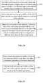
- FIG. 19 is schematic structural diagram of an electronic device according to the present disclosure.
- FIG. 20 is a schematic flow chart of a preparing method of a touch apparatus according to the present disclosure.
- FIG. 21 is a schematic flow chart of a preparing method of a touch electrode according to the present disclosure.
- FIG. 22 is a schematic flow chart of a preparing method according to the present disclosure.
- a touch electrode is generally made of metal or ITO. If a touch sensor is bent, the touch electrode will be deformed at the bending position, which causes the touch electrode to be easily broken at the bent portion, and results in a low service life of the touch sensor.
- the touch apparatus includes a substrate, a cover plate, a first touch sensor and a second touch sensor.
- the substrate and the cover plate are arranged opposite to each other.
- the substrate includes a display region, and the display region includes a first display region and a second display region arranged in a first direction.
- the first touch sensor is arranged on the side of the cover plate towards the substrate.
- the second touch sensor is arranged on the side of the substrate towards the cover plate.
- the second touch sensor is arranged in a different layer from the first touch sensor.
- the first direction is parallel to the substrate.
- the first touch sensor has a first projection on the substrate in a second direction, and the first projection covers the first display region.
- the second touch sensor has a second projection on the substrate in the second direction, and the second projection covers the second display region.
- the second direction is perpendicular to the substrate.
- the first touch sensor and the second touch sensor are arranged in a separate manner in the display region. In such way, when the touch apparatus is bent at the junction of the first display region and the second display region is bent, the touch electrode can be prevented from being broken, which improves the service life.
- the first touch sensor is arranged in a different layer from the second touch sensor, and wires of the first touch sensor may overlap wires of the second touch sensor in the second direction, which facilitates the wire layout of the first touch sensor and the second touch sensor and saves wire space.
- FIG. 1 is a schematic structural diagram of a touch apparatus according to the present disclosure.
- the touch apparatus includes a substrate 11 , a cover plate 12 , a first touch sensor 13 , and a second touch sensor 14 .
- the substrate 11 and the cover plate 12 are arranged opposite to each other.
- the substrate 11 is includes a display region, and the display region includes a first display region A and a second display region B arranged in a first direction Y.
- the first touch sensor 13 is arranged on the side of the cover plate 12 towards the substrate 11 .
- the second touch sensor 14 is arranged on the side of the substrate 11 towards the cover plate 12 .
- the second touch sensor 14 is arranged in a different layer from the first touch sensor 13 .
- the first direction Y is parallel to the substrate 11 .
- the first touch sensor 13 has a first projection on the substrate 11 in a second direction Z, and the first projection covers the first display region A.
- the second touch sensor 14 has a second projection on the substrate 11 in the second direction, and the second projection covers the second display region B.
- the second direction Z is perpendicular to the substrate 11 .
- each of the cover plate 12 and the substrate 11 may be flexible plate.
- the flexible plate may be PET (polyethylene terephthalate), or a PET substrate, or a COP (cyclic olefin copolymer) substrate.
- the first touch sensor 13 may be not overlapped, or be partially overlapped with the second touch sensor 14 .
- FIG. 2 is a schematic diagram of a relative position relation of two touch sensors of a touch apparatus according to the present disclosure.
- the first projection of the first touch sensor 13 on the substrate 11 is completely located in the first display region A
- the second projection of the second touch sensor 14 on the substrate 11 is completely located in the second display region B.
- the sum of the areas of the first projection and the second projection is equal to the area of the display region C.
- a third direction X is parallel to the substrate 11 and is perpendicular to the first direction Y.
- the first direction Y, the second direction Z, and the third direction X are three corresponding coordinate axes of an XYZ rectangular coordinate system.
- the structure of the touch apparatus may be as shown in FIG. 3 , which is a schematic diagram of a relative position relation of two touch sensors of a touch apparatus according to the present disclosure.
- the first projection of the first touch sensor 13 on the substrate 11 is completely located in the first display region A
- the second projection of the second touch sensor 14 on the substrate 11 is completely located in the second display region B.
- a gap K with a preset width in the first direction Y exists between the first projection and the second projection. The width of the gap K in the first direction Y is not greater than 10 ⁇ m.
- first touch sensor 13 and the second touch sensor 14 are arranged in the same layer in the second direction Z, a gap with a larger width should be designed between the first touch sensor 13 and the second touch sensor 14 to achieve the insulation between them, which may seriously affect the accuracy of touch detection.
- the insulation between the first touch sensor 13 and the second touch sensor 14 can be achieved via the gap K having a width in the first direction Y not greater than 10 ⁇ m, which makes the touch apparatus have a good touch detection accuracy meeting application requirements with a sufficient width of the gap K between the first touch sensor 13 and the second touch sensor 14 .
- the width of the gap K may be 2 mm, or 5 ⁇ m.
- the structure of the touch apparatus may be as shown in FIG. 4 , which is a schematic structural diagram of a touch apparatus according to the present disclosure.
- the first projection of the first touch sensor 13 on the substrate 11 and the second projection of the second touch sensor 14 on the substrate 11 have an overlapping portion D with a preset width in the first direction Y.
- the width of the overlapping portion D in the first direction Y is not greater than 10 ⁇ m.
- the two touch sensors are designed to be partially overlapped, there is no need to perform a highly precise position calibration, and there is no touch dead zone.
- FIG. 5 is a schematic structural diagram of a touch apparatus according to the present disclosure.
- the touch apparatus as shown in FIG. 5 further includes a flexible display panel 15 .
- the flexible display panel 15 is attached to the substrate 11 .
- the flexible display panel 15 is arranged on the side of the substrate 11 facing away from the cover plate 12 .
- the first touch sensor 13 and the second touch sensor 14 may be prepared separately from the flexible display panel 15 .
- the substrate 11 may be a flexible display substrate.
- the structure of the substrate 11 may be as shown in FIG. 6 , which is a schematic structural diagram of a touch apparatus according to the present disclosure.
- the substrate 11 is a flexible display substrate, and the flexible display substrate includes multiple pixel units 113 arranged in an array.
- the flexible display substrate further includes a flexible back plate 111 and an encapsulation layer 112 .
- the multiple pixel units 113 are arranged on the side of the flexible back plate 111 towards the cover plate 12 , and the encapsulation layer 112 covers all of the multiple pixel units 113 .
- the second touch sensor 14 is arranged on the side of the encapsulation layer 112 towards the cover plate 12 .
- the structure of the touch apparatus may also be as shown in FIG. 7 , which is a schematic structural diagram of a touch apparatus according to the present disclosure.
- the substrate 11 is also a flexible display substrate.
- the embodiment shown in FIG. 7 differs from that in FIG. 6 in that, the flexible back plate 111 in FIG. 7 is arranged towards the cover plate 12 , and the second touch sensor 14 is arranged on the side of the flexible back plate 111 towards the cover plate 12 .
- Pixel units 113 are arranged on the side of the flexible back plate 111 facing away from the cover plate 12 .
- the encapsulation layer 112 covers all the pixel units 113 .
- the flexible display substrate directly severs as the substrate of the second touch sensor, which can reduce the thickness of the touch apparatus and simplify the fabrication process.
- each of the first touch sensor 13 and the second touch sensor 14 is provided with an independent control chip.
- the first touch sensor 13 and the second touch sensor 14 are in different layers in the second direction Z, sensing distances are different, and detected signal intensities are different, which results in a detection difference between the two touch sensors.
- separate control chips are provided to perform independent touch detection control on the two touch sensors, which can avoid the detection difference between the two touch sensors.
- FIG. 8 is a schematic structural diagram of a touch apparatus according to the present disclosure.
- FIG. 9 is a top view of a substrate in the touch apparatus shown in FIG. 8 .
- the touch apparatus further includes a control chip 131 for the first touch sensor 13 and a control chip 141 for the second touch sensor 14 .
- the substrate 11 further includes a frame region D surrounding the display region C.
- Both the control chip 131 for the first touch sensor 13 and the control chip 141 for the second touch sensor 14 are arranged in the frame region D.
- the two control chips in FIG. 9 are both arranged in the frame region D corresponding to two opposite sides of the display region C. Positions of the two chips includes, but not limited to the positions shown in FIG. 9 .
- the two control chips may further arranged in the frame region D corresponding to the two adjacent sides of the display region C.
- the first touch sensor 13 and the second touch sensor 14 are electrically connected to their corresponding control chips through a flexible circuit board.
- the first touch sensor 13 may be electrically connected to the control chip 131 through the corresponding flexible circuit board.
- the second touch sensor 14 may be electrically connected to the control chip 141 through the corresponding flexible circuit board. Since the second touch sensor and the control chip 141 are located on the same surface of the substrate 11 , the second touch sensor 14 may also be electrically connected to the control chip 141 directly through conductive wires formed on the surface of the substrate 11 .
- the structure of the touch apparatus may be as shown in FIG. 10 , which is a schematic structural diagram of a touch apparatus according to the present disclosure.
- the control chip 131 for the first touch sensor 13 is arranged on a surface of the cover plate 12 towards the substrate 11
- the control chip 141 for the second touch sensor 14 is arranged on a surface of the substrate 11 towards the cover plate 12 .
- the control chip 141 is located in the frame region. In the second direction Z, the projection of the control chip 131 on the substrate 11 is located in the frame region.
- the two touch sensors of the touch apparatus may have the same control chip.
- the structure of the touch apparatus is as shown in FIG. 11 , which is a schematic structural diagram of a touch apparatus according to the present disclosure.
- the touch apparatus as shown in FIG. 11 further includes a control chip 10 .
- the control chip 10 is arranged in the frame region of the substrate 11 .
- the first touch sensor 13 and the second touch sensor 14 share the same control chip 10 .
- a conductive member 20 is arranged between the substrate 11 and the cover plate 12 .
- the conductive member 20 electrically connects the first touch sensor 13 to the substrate 11 .
- the first touch sensor 13 and the second touch sensor 14 are electrically connected to the control chip 10 through the conductive wires arranged on the substrate 11 .
- the two touch sensors have a difference in the touch detection due to a height difference between the two touch sensors in the second direction Z.
- the second touch sensor 14 needs a higher sensing precision than the first touch sensor 13 , and thus the sensing precision of the control chip may be set to be not lower than the minimum sensing precision of the second touch sensor 14 .
- the first touch sensor 13 can sense any touch operation detectable to the second touch sensor 14 , thereby eliminating the difference in touch detection caused by the height difference between the two touch sensors.
- the substrate 11 is an OLED display panel
- Each of the multiple pixel units is an OLED device.
- the OLED device includes an anode arranged on the surface of the back plate, a light emitting functional layer arranged on the back side of the anode, and a cathode arranged on the light emitting functional layer.
- the conductive member 20 may be conductive glue.
- the first touch sensor 13 is electrically connected to the conductive wires on the surface of the substrate 11 via the conductive glue directly, and thereby electrically connected to the control chip 10 .
- the conductive wires connected to the conductive member 20 may be prepared in the same conductive layer as the anode of the OLED display panel.
- the structure of the touch apparatus may be further as shown in FIG. 12 , which is a schematic structural diagram of a touch apparatus according to the present disclosure.
- the touch apparatus as shown in FIG. 12 further includes a control chip 10 .
- the control chip 10 is arranged in the frame region of the substrate 11 .
- the first touch sensor 13 and the second touch sensor 14 share the same control chip 10 .
- a conductive member 20 is provided between the substrate 11 and the cover plate 12 . The conductive member 20 electrically connects the first touch sensor 13 to the substrate 11 .
- the OLED includes a flexible back plate 111 and multiple pixel units 113 arranged on the side of the flexible back plate III towards the cover plate 12 .
- Each of the multiple pixel units 113 is an OLED device.
- the OLED device includes an anode c and a cathode a which are arranged opposite to each other, and a light emitting layer b arranged between the anode c and the cathode a.
- the cathode b of each OLED device is a unitary structure, and the light emitting layer h of each OLED device is a unitary structure.
- the anodes c of the OLED devices are arranged in an array independently.
- the first touch sensor 13 and the second touch sensor 14 are electrically connected to the control chip 10 through the conductive wires arranged on the substrate 11 .
- the wires and the anode c are prepared in the same conductive layer.
- the conductive member 20 includes a support column 201 and a connection layer 202 arranged on the surface of the support column 201 .
- the connection layer 202 and the cathode a are prepared in the same conductive layer.
- the support column 201 also serves as a support for the conductive member 20 , which can reduce the usage of the conductive material and reduce the cost.
- the conductive member 20 via which the first touch sensor 13 is connected to the wires on the surface of the substrate 11 , may be constituted by a cathode metal layer.
- the cathode metal layer completely serves as the conductive member 20 without being supported by the support column.
- the structure of the electrode of the first touch sensor and the second touch sensor may be a mutual-capacitance electrode structure as shown in FIG. 13 .
- FIG. 13 is a schematic structural diagram of an electrode of a touch sensor according to the present disclosure.
- the structure of the electrode of the touch sensor includes a touch detection electrode 51 and a touch driving electrode 52 .
- the touch detection electrode 51 includes multiple strip electrodes arranged in parallel.
- the touch driving electrode 52 includes multiple strip electrodes arranged in parallel.
- the multiple strip electrodes of the touch detection electrode 51 are perpendicular to the multiple strip electrodes of the touch driving electrode 52 .
- the touch detection electrode 51 and the touch driving electrode 52 are located in different conductive layers, with an insulating layer between them.
- the flexible display panel in the above embodiments is only an example of the OLED panel. It should be understood by those skilled in the art that the flexible display panel in the embodiments of the present disclosure may further be other types of display panels, such as liquid crystal display panel, or electronic paper. Accordingly, the conductive member may be a conductive structure arranged inside a flexible panel or between a flexible panel and a cover plate, such as an optical gap material with a conductivity in a liquid crystal panel, or a pixel electrode layer or a common electrode layer on a thin film transistor (TFT) substrate.
- TFT thin film transistor
- FIG. 14 is a schematic structural diagram of an electrode of a touch sensor according to the present disclosure.
- the touch detection electrode 51 includes multiple sub-electrodes arranged in parallel. Each of the multiple sub-electrodes includes multiple rhombic electrodes connected in series. All the sub-electrodes of the touch detection electrode 51 are located in a same conductive layer.
- the touch driving electrode 52 includes multiple sub-electrodes arranged in parallel.
- Each of the multiple sub-electrodes includes multiple rhombic electrodes connected in series via bridges 53 and via-holes 54 .
- the rhombic electrodes of the touch driving electrode 52 are located in the same conductive layer as the sub-electrodes of the touch detection electrode 51 .
- the bridges 53 and the rhombic electrodes of the touch driving electrode 52 are located in different conductive layers, and there is an insulating layer between the bridges 53 and the conductive layer.
- the touch detection principles in FIG. 14 are the same as that in FIG. 13 , which will not be described herein.
- the electrode structure of the first touch sensor and the second touch sensor may further be a mutual-capacitance electrode structure as shown in FIG. 15 .
- FIG. 15 is a schematic structural diagram of an electrode of a touch sensor according to the present disclosure.
- the electrode structure of the touch sensor includes a detection electrode 61 and a reference electrode 62 .
- the touch sensor includes multiple detection electrodes 61 arranged in an array.
- the detection electrode 61 and the reference electrode 62 are located in different conductive layers and are insulated with each other. In touch detection, the detection electrode 61 inputs a detection signal, and the touch position is detected based on the output signal of the detection electrode 61 .
- FIG. 16 is a schematic diagram of principles of a touch apparatus for reducing a touch dead zone according to the present disclosure.
- FIG. 17 is a schematic diagram of principles of a touch apparatus for achieving a narrow border according to the present disclosure.
- a touch apparatus is shown in the left diagram of FIG. 16 , in which the first touch sensor 13 and the second touch sensor 14 are arranged in different layers. In the right diagram of FIG. 16 , the first touch sensor 13 and the second touch sensor 14 are arranged in the same layer.
- the first touch sensor 13 and the second touch sensor 14 are arranged in the same layer, a large gap 161 needs to be arranged between the first touch sensor 13 and the second touch sensor 14 for electrical insulation, which results in a large touch dead zone.
- the first touch sensor 13 and the second touch sensor 14 are arranged in different layers. In such way, the first touch sensor 13 and the second touch sensor 14 may be completely or partially overlapped, or have a small gap in the second direction Z, leading to a small or zero touch dead zone.
- the left diagram of FIG. 17 is a schematic diagram of wire layout of a touch apparatus according to the present disclosure
- the right diagram of FIG. 17 is a conventional wire layout.
- the wires 160 corresponding to the first touch sensor 13 may be prepared in a separate conductive layer
- the wires 160 corresponding to the second touch sensor 14 may be prepared in a separate conductive layer, which significantly shortens the width occupied by the wires 160 and reduces the frame region.
- the first touch sensor 13 may be formed on a surface of the cover plate towards the substrate.
- the second touch sensor 14 may be formed on a surface of the substrate towards the cover plate, and the substrate is attached to the cover plate.
- both the first touch sensor and the second touch sensor may be arranged on a same surface of the cover plate, a first insulating layer is arranged between the first touch sensor and the second touch sensor for electrical insulation, and the side of cover plate provided with the second touch sensor is attached to the substrate.
- both the first touch sensor and the second touch sensor may be arranged on a surface of the substrate, a first insulating layer is arranged between the first touch sensor and the second touch sensor for electrical insulation, and the side of the substrate provided with the first touch sensor is attached to the cover plate.
- the first insulating layer may be a flexible transparent sheet, which can be attached to the first touch sensor, such as a polymer film, or an organic or inorganic insulating film which is deposited on the surface of the first touch sensor, or the second touch sensor in a subsequent process, which depends on specific situations, and is not limited in the present disclosure.
- FIG. 18 is a schematic diagram of a result of a touch apparatus according to the present disclosure.
- This touch apparatus differs from the embodiment as shown in FIG. 1 in that a flexible plate 180 is arranged between the first touch sensor 13 and the second touch sensor 14 .
- a touch panel with first touch sensor 13 and a touch panel with the second touch sensor 14 may be prepared separately, and the touch panels are attached to the cover plate 12 and the substrate 11 , respectively.
- the first touch sensor 13 is formed on the cover plate 12
- the flexible plate 180 is attached to the surface of the first touch sensor 13
- the second touch sensor 14 is formed on the surface of the flexible plate 180 facing away from the first touch sensor 13
- the substrate 11 is attached to the surface of the second touch sensor 14 .
- the second touch sensor 14 is formed on the substrate 11
- the flexible plate 180 is attached to the surface of the second touch sensor 14
- the first touch sensor 13 is formed on the surface of the flexible plate 180 facing away from the second touch sensor 14
- the cover plate 12 is attached to the first touch sensor 13 .
- the electrode structures of the first touch sensor and the second touch sensor in the present disclosure are not limited to the above-described mutual-capacitance electrode structure.
- the electrode structures of the first touch sensor and the second touch sensor may also be a self-capacitance electrode structure, or one of the first touch sensor and the second touch sensor has the mutual-capacitance electrode structure, and the other has the self-capacitance electrode structure, which depends on specific situations, and is not limited in the present disclosure.
- the first touch sensor and the second touch sensor are arranged.
- the touch electrode can be prevented from being broken, which improves the service life.
- the first touch sensor is arranged in a different layer from the second touch sensor, and the wires of the first touch sensor may overlap the wires of the second touch sensor in the second direction, which facilitates the wire layout of the first touch sensor and the second touch sensor and saves wire space.
- an electronic device is further provided according to the present disclosure.
- the electronic device is shown in FIG. 19 , which is a schematic structural diagram of an electronic device according to the present disclosure.
- the electronic device includes a touch apparatus 71 , and the touch apparatus 71 is the touch apparatus according to the above embodiments.
- the electronic device may be an electronic device with a touch display function, such as a mobile phone, a tablet computer, or a television.
- the above touch apparatus is adopted in the electronic device, which can prevent the touch electrode from being broken when bending the electronic device, thereby improving the service life.
- wires of the first touch sensor may overlap wires of the second touch sensor in the second direction, which facilitates the wire layout of the first touch sensor and the second touch sensor and saves wire space.
- a preparing method is further provided according to the present disclosure to prepare the above touch apparatus.
- the preparing method includes steps S 11 to S 13 .
- a substrate and a cover plate are provided.
- the substrate includes a display region, and the display region includes a first display region and a second display region arranged in a first direction.
- step S 12 a first touch sensor is formed on a surface of the cover plate, and a second touch sensor is formed on a surface of the substrate.
- step S 12 includes: forming touch electrodes on the surfaces of the first touch sensor and the second touch sensor in a same process.
- Each of the touch electrodes includes a touch detection electrode and a touch driving electrode.
- the transmittance and the resistivity of the touch detection of the two touch sensors are the main factor affecting the transmittance and the resistivity of the first touch sensor and the second touch sensor. If the two touch sensors are prepared in different times and in different processes, the two touch sensors have a great difference in the transmittance and resistivity, which may affect the touch detection accuracy of the touch apparatus. Touch electrodes of the two touch sensors are prepared in the same process at the same time, which can avoid the difference in the touch electrodes of the two touch sensors.
- step S 12 may further as shown in FIG. 21 , which is a schematic flow chart of a preparing method of a touch electrode according to the present disclosure.
- the preparing method includes steps S 21 and S 22 .
- step S 21 a touch electrode is formed on a surface of one of the substrate and the cover plate, and a formation parameter of the touch electrode is detected.
- step S 22 a touch electrode is formed on a surface of the other one of the substrate and the cover plate based on the formation parameter.
- parameter monitoring is performed by taking the process of preparing the touch electrode of one of the first touch sensor and the second touch sensor as a master test pattern, and the touch electrode of the other one of the first touch sensor and the second touch sensor are prepared based on the parameter monitoring to ensure the consistency of the transmittance and the electrical parameters.
- step S 13 the cover plate is attached to the substrate.
- the side of the cover plate provided with the first touch sensor is arranged opposite to the side of the substrate provided with the second touch sensor.
- the second touch sensor and the first touch sensor are in different layers.
- the first direction is parallel to the substrate.
- the first touch sensor has a first projection on the substrate in a second direction, and the first projection covers the first display region.
- the second touch sensor has a second projection on the substrate in the second direction, and the second projection covers the second display region.
- the second direction is perpendicular to the substrate.
- each of the two touch sensors may be provided with an independent control chip.
- the preparing method further includes: electrically connecting a first control chip to the first touch sensor, and electrically connecting a second control chip to the second touch sensor.
- the first control chip drives the first touch sensor to perform touch detection
- the second control chip drives the second touch sensor to perform touch detection, to reduce the touch error of the first touch sensor and the second touch sensor due to the relative height between the first touch sensor and the second touch sensor.
- a preparing method is further provided according to the present disclosure.
- the preparing method includes is as shown in FIG. 22 , which is a schematic flow chart of a preparing method according to the present disclosure.
- the preparing method includes steps S 31 to S 35 .
- step S 31 a substrate and a cover plate are provided.
- step S 32 a first touch sensor is formed on a side of the cover plate.
- step S 33 a first insulating layer is formed, which covers at least a part of the first touch sensor.
- step S 34 a second touch sensor is prepared on the cover plate on which the first insulation layer is formed, where the first insulating layer electrically insulates the first touch sensor from the second touch sensor.
- step S 35 the substrate is attached to the side of the cover plate prepared with the second touch sensor.
- the first direction is parallel to the substrate.
- the first touch sensor has a first projection on the substrate in a second direction, and the first projection covers the first display region.
- the second touch sensor has a second projection on the substrate in the second direction, and the second projection covers the second display region.
- the second direction is perpendicular to the substrate.
- the preparing method may include: providing a flexible plate; forming a first touch sensor on one side of the flexible plate, and forming a second touch sensor on the other side of the flexible plate; attaching a cover plate to the side of the flexible plate arranged with the first touch sensor, and attaching a substrate to the side of the flexible plate arranged with the second touch sensor.
- the first direction is parallel to the substrate.
- the first touch sensor has a first projection on the substrate in a second direction, and the first projection covers the first display region.
- the second touch sensor has a second projection on the substrate in the second direction, and the second projection covers the second display region.
- the second direction is perpendicular to the substrate.
- the preparing method may include: forming a first touch sensor on a cover plate 12 , attaching a flexible plate to the surface of the first touch sensor, forming a second touch sensor on the surface of the flexible plate facing away from the first touch sensor, and attaching a substrate to the surface of the second touch sensor, so as to complete the preparing of the touch apparatus.
- the preparing method may include: forming a second touch sensor on a substrate, attaching a flexible plate to the surface of the second touch sensor, forming a first touch sensor on the surface of the flexible plate facing away from the second touch sensor, and attaching a cover plate to the surface of the first touch sensor, so as to complete the preparing of the touch apparatus.
- the touch electrode can be prevented from being broken, which improves the service life.
- wires of the first touch sensor may overlap wires of the second touch sensor in the second direction, which facilitates the wire layout of the first touch sensor and the second touch sensor and saves wire space.
- the touch electrodes of the two touch sensors have good consistency of transmittance and resistivity, ensuring a high detection precision of the touch apparatus.
- Embodiments are described in a progressive manner and each embodiment places emphasis on the difference from other embodiments. Therefore, one embodiment can refer to other embodiments for the same or similar parts. Since the method disclosed in the embodiments corresponds to the apparatus disclosed in the embodiments, the description of the method is simple, and reference may be made to the relevant part of the apparatus.
Landscapes
- Engineering & Computer Science (AREA)
- Theoretical Computer Science (AREA)
- General Engineering & Computer Science (AREA)
- Human Computer Interaction (AREA)
- Physics & Mathematics (AREA)
- General Physics & Mathematics (AREA)
- Computer Hardware Design (AREA)
- Computer Networks & Wireless Communication (AREA)
- Microelectronics & Electronic Packaging (AREA)
- User Interface Of Digital Computer (AREA)
- Push-Button Switches (AREA)
- Position Input By Displaying (AREA)
Abstract
Description
-
- providing a substrate and a cover plate, where the substrate includes a display region, and the display region includes a first display region and a second display region arranged in a first direction;
- forming a first touch sensor on a surface of the cover plate, and forming a second touch sensor on a surface of the substrate; and
- attaching the cover plate to the substrate, where the side of the cover plate provided with the first touch sensor is arranged opposite to the side of the substrate provided with the second touch sensor, and the second touch sensor is arranged in a different layer from the first touch sensor.
-
- providing a substrate and a cover plate;
- forming a first touch sensor on a side of the cover plate;
- forming a first insulating layer, which covers at least a part of the first touch sensor;
- preparing a second touch sensor on the cover plate on which the first insulation layer is formed, where the first insulating layer electrically insulates the first touch sensor from the second touch sensor; and
- attaching the substrate to the side of the cover plate prepared with the second touch sensor.
Claims (16)
Applications Claiming Priority (3)
| Application Number | Priority Date | Filing Date | Title |
|---|---|---|---|
| CN201610970032 | 2016-10-28 | ||
| CN201610970032.3A CN106502466B (en) | 2016-10-28 | 2016-10-28 | Touch device, electronic equipment and manufacturing method |
| CN201610970032.3 | 2016-10-28 |
Publications (2)
| Publication Number | Publication Date |
|---|---|
| US20170277310A1 US20170277310A1 (en) | 2017-09-28 |
| US10649589B2 true US10649589B2 (en) | 2020-05-12 |
Family
ID=58321841
Family Applications (1)
| Application Number | Title | Priority Date | Filing Date |
|---|---|---|---|
| US15/622,022 Active US10649589B2 (en) | 2016-10-28 | 2017-06-13 | Touch apparatus, electronic device and preparing method |
Country Status (2)
| Country | Link |
|---|---|
| US (1) | US10649589B2 (en) |
| CN (1) | CN106502466B (en) |
Families Citing this family (12)
| Publication number | Priority date | Publication date | Assignee | Title |
|---|---|---|---|---|
| KR102318556B1 (en) * | 2017-04-12 | 2021-10-29 | 현대자동차주식회사 | Input apparatus and control method of the same |
| CN107203296B (en) * | 2017-05-25 | 2020-12-25 | 上海天马微电子有限公司 | Display panel, manufacturing method thereof and display device |
| KR102452251B1 (en) * | 2017-08-04 | 2022-10-11 | 삼성디스플레이 주식회사 | Display apparatus |
| CN109558025B (en) * | 2017-09-27 | 2024-04-02 | 京东方科技集团股份有限公司 | Touch panel, manufacturing method thereof and display device |
| CN110945463A (en) * | 2017-11-24 | 2020-03-31 | 深圳市柔宇科技有限公司 | Touch screen and terminal |
| CN107831959A (en) * | 2017-12-12 | 2018-03-23 | 信利光电股份有限公司 | A kind of capacitive touch screen of repeatable bending |
| CN110275647B (en) * | 2018-03-13 | 2021-01-12 | 京东方科技集团股份有限公司 | Touch structure and manufacturing method thereof, touch device and touch positioning method |
| CN108461528B (en) * | 2018-03-23 | 2020-10-23 | 武汉华星光电技术有限公司 | OLED spliced display and splicing method thereof |
| US10852869B2 (en) * | 2018-12-14 | 2020-12-01 | Wuhan China Star Optoelectronics Semiconductor Display Technology Co., Ltd. | Narrow border touch display apparatus |
| KR20210002163A (en) * | 2019-06-26 | 2021-01-07 | 삼성디스플레이 주식회사 | Electronic panel and electronic apparatus including the same |
| CN113641265B (en) * | 2021-08-13 | 2023-10-31 | 武汉华星光电技术有限公司 | Touch panel and touch driving method |
| CN114637429B (en) * | 2022-03-31 | 2023-05-05 | 业成科技(成都)有限公司 | Embedded touch transparent display device |
Citations (12)
| Publication number | Priority date | Publication date | Assignee | Title |
|---|---|---|---|---|
| CN102799313A (en) | 2012-05-07 | 2012-11-28 | 友达光电股份有限公司 | Touch panel, touch display panel and touch display device |
| CN203311375U (en) | 2013-06-03 | 2013-11-27 | 南昌欧菲光科技有限公司 | Touch screen lead structure |
| CN203552211U (en) | 2013-08-20 | 2014-04-16 | 信利光电股份有限公司 | Touch screen with narrow frame |
| US20150008115A1 (en) | 2013-07-08 | 2015-01-08 | Sony Corporation | Touch sensing component and method for manufacturing the same, touch screen and electronic device |
| CN204143398U (en) | 2014-05-30 | 2015-02-04 | 和鑫光电股份有限公司 | Bendable touch-control sensing module and display device thereof |
| CN104597646A (en) | 2014-12-22 | 2015-05-06 | 上海天马微电子有限公司 | Display panel and display device |
| US20150193065A1 (en) * | 2014-01-08 | 2015-07-09 | E Ink Holdings Inc. | Touch panel module and touch display device having the same |
| US20150241924A1 (en) * | 2014-02-27 | 2015-08-27 | Industrial Technology Research Institute | Touch panel |
| TW201533624A (en) | 2014-02-27 | 2015-09-01 | Ind Tech Res Inst | Touch panel and sensing method thereof |
| CN105224116A (en) | 2014-06-12 | 2016-01-06 | 宸鸿科技(厦门)有限公司 | A kind of contact panel |
| US20160179268A1 (en) | 2014-12-18 | 2016-06-23 | Samsung Display Co., Ltd. | Touch sensor device |
| US20170315645A1 (en) * | 2016-04-27 | 2017-11-02 | Samsung Display Co., Ltd. | Flexible display device and method of manufacturing the same |
-
2016
- 2016-10-28 CN CN201610970032.3A patent/CN106502466B/en active Active
-
2017
- 2017-06-13 US US15/622,022 patent/US10649589B2/en active Active
Patent Citations (14)
| Publication number | Priority date | Publication date | Assignee | Title |
|---|---|---|---|---|
| CN102799313A (en) | 2012-05-07 | 2012-11-28 | 友达光电股份有限公司 | Touch panel, touch display panel and touch display device |
| CN203311375U (en) | 2013-06-03 | 2013-11-27 | 南昌欧菲光科技有限公司 | Touch screen lead structure |
| US20150008115A1 (en) | 2013-07-08 | 2015-01-08 | Sony Corporation | Touch sensing component and method for manufacturing the same, touch screen and electronic device |
| CN104281304A (en) | 2013-07-08 | 2015-01-14 | 索尼公司 | Touch induction component, manufacturing method, touch screen and electronic device |
| CN203552211U (en) | 2013-08-20 | 2014-04-16 | 信利光电股份有限公司 | Touch screen with narrow frame |
| US20150193065A1 (en) * | 2014-01-08 | 2015-07-09 | E Ink Holdings Inc. | Touch panel module and touch display device having the same |
| TW201533624A (en) | 2014-02-27 | 2015-09-01 | Ind Tech Res Inst | Touch panel and sensing method thereof |
| US20150241924A1 (en) * | 2014-02-27 | 2015-08-27 | Industrial Technology Research Institute | Touch panel |
| CN204143398U (en) | 2014-05-30 | 2015-02-04 | 和鑫光电股份有限公司 | Bendable touch-control sensing module and display device thereof |
| CN105224116A (en) | 2014-06-12 | 2016-01-06 | 宸鸿科技(厦门)有限公司 | A kind of contact panel |
| US20160179268A1 (en) | 2014-12-18 | 2016-06-23 | Samsung Display Co., Ltd. | Touch sensor device |
| CN104597646A (en) | 2014-12-22 | 2015-05-06 | 上海天马微电子有限公司 | Display panel and display device |
| US20160179262A1 (en) | 2014-12-22 | 2016-06-23 | Shanghai Tianma Micro-electronics Co., Ltd. | Display panel and display device |
| US20170315645A1 (en) * | 2016-04-27 | 2017-11-02 | Samsung Display Co., Ltd. | Flexible display device and method of manufacturing the same |
Non-Patent Citations (2)
| Title |
|---|
| CN First Office Action dated Oct. 26, 2018 in the corresponding Chinese application(application No. 201610970032.3). |
| Second Office Action for CN Appln. No. 201610970032.3 dated Mar. 25, 2019, 17 pages. |
Also Published As
| Publication number | Publication date |
|---|---|
| US20170277310A1 (en) | 2017-09-28 |
| CN106502466B (en) | 2020-04-14 |
| CN106502466A (en) | 2017-03-15 |
Similar Documents
| Publication | Publication Date | Title |
|---|---|---|
| US10649589B2 (en) | Touch apparatus, electronic device and preparing method | |
| US10430013B2 (en) | Touch substrate and manufacturing method thereof, display device, fingerprint determination device and method for determining fingerprint | |
| US10088941B2 (en) | Touch control substrate and display device | |
| CN106940605B (en) | Display panel | |
| WO2020029371A1 (en) | Touchscreen and oled display panel | |
| US9671638B2 (en) | High-accuracy in-cell touch panel structure of narrow border | |
| KR20110093069A (en) | Organic light emitting diode display and method for manufacturing the same | |
| US10782832B2 (en) | Mobile terminal and touch screen with a notch area | |
| US20210286468A1 (en) | Touch Panel and Manufacturing Method Therefor, and Touch Display Device | |
| US20110096019A1 (en) | Touch panel and touch display device | |
| US20190235668A1 (en) | Touch screen and mobile terminal | |
| US10698548B2 (en) | Touch panel and organic light emitting diode display panel | |
| KR20200012058A (en) | Touch member and display device with the same | |
| US11216144B2 (en) | Touch structure, touch display panel and driving method | |
| US9563301B2 (en) | Array substrate, fabricating method thereof and display device | |
| KR20110120046A (en) | Touch screen panel and display device having the same | |
| US10620735B2 (en) | Force touch module, manufacturing method thereof, display screen and display device | |
| US10768753B2 (en) | Touch display panel, display device and touch panel | |
| CN113741730A (en) | Display device | |
| US11086460B2 (en) | Touch substrate, method for manufacturing same, and touch device | |
| US10359873B2 (en) | Touch display screen | |
| US11989368B2 (en) | Display panel and display device | |
| US10488694B2 (en) | In-cell touch panel and display device | |
| CN212586865U (en) | Touch display panel and display device | |
| US11861119B2 (en) | Display panel and method for manufacturing the same, and display apparatus |
Legal Events
| Date | Code | Title | Description |
|---|---|---|---|
| AS | Assignment |
Owner name: SHANGHAI TIANMA AM-OLED CO., LTD., CHINA Free format text: ASSIGNMENT OF ASSIGNORS INTEREST;ASSIGNORS:XIONG, ZHIYONG;LIN, FANGYUN;REEL/FRAME:042700/0714 Effective date: 20170606 Owner name: TIANMA MICRO-ELECTRONICS CO., LTD., CHINA Free format text: ASSIGNMENT OF ASSIGNORS INTEREST;ASSIGNORS:XIONG, ZHIYONG;LIN, FANGYUN;REEL/FRAME:042700/0714 Effective date: 20170606 |
|
| STPP | Information on status: patent application and granting procedure in general |
Free format text: FINAL REJECTION MAILED |
|
| STPP | Information on status: patent application and granting procedure in general |
Free format text: RESPONSE AFTER FINAL ACTION FORWARDED TO EXAMINER |
|
| STPP | Information on status: patent application and granting procedure in general |
Free format text: ADVISORY ACTION MAILED |
|
| STPP | Information on status: patent application and granting procedure in general |
Free format text: DOCKETED NEW CASE - READY FOR EXAMINATION |
|
| STPP | Information on status: patent application and granting procedure in general |
Free format text: NON FINAL ACTION MAILED |
|
| STPP | Information on status: patent application and granting procedure in general |
Free format text: FINAL REJECTION MAILED |
|
| STPP | Information on status: patent application and granting procedure in general |
Free format text: DOCKETED NEW CASE - READY FOR EXAMINATION |
|
| STCF | Information on status: patent grant |
Free format text: PATENTED CASE |
|
| AS | Assignment |
Owner name: TIANMA MICRO-ELECTRONICS CO., LTD., CHINA Free format text: ASSIGNMENT OF ASSIGNORS INTEREST;ASSIGNORS:SHANGHAI TIANMA AM-OLED CO.,LTD.;TIANMA MICRO-ELECTRONICS CO., LTD.;REEL/FRAME:059619/0730 Effective date: 20220301 Owner name: WUHAN TIANMA MICROELECTRONICS CO., LTD.SHANGHAI BRANCH, CHINA Free format text: ASSIGNMENT OF ASSIGNORS INTEREST;ASSIGNORS:SHANGHAI TIANMA AM-OLED CO.,LTD.;TIANMA MICRO-ELECTRONICS CO., LTD.;REEL/FRAME:059619/0730 Effective date: 20220301 Owner name: WUHAN TIANMA MICRO-ELECTRONICS CO., LTD., CHINA Free format text: ASSIGNMENT OF ASSIGNORS INTEREST;ASSIGNORS:SHANGHAI TIANMA AM-OLED CO.,LTD.;TIANMA MICRO-ELECTRONICS CO., LTD.;REEL/FRAME:059619/0730 Effective date: 20220301 |
|
| MAFP | Maintenance fee payment |
Free format text: PAYMENT OF MAINTENANCE FEE, 4TH YEAR, LARGE ENTITY (ORIGINAL EVENT CODE: M1551); ENTITY STATUS OF PATENT OWNER: LARGE ENTITY Year of fee payment: 4 |