US10636506B2 - Methods for testing a storage unit and apparatuses using the same - Google Patents
Methods for testing a storage unit and apparatuses using the same Download PDFInfo
- Publication number
- US10636506B2 US10636506B2 US15/663,958 US201715663958A US10636506B2 US 10636506 B2 US10636506 B2 US 10636506B2 US 201715663958 A US201715663958 A US 201715663958A US 10636506 B2 US10636506 B2 US 10636506B2
- Authority
- US
- United States
- Prior art keywords
- test
- data
- ecc
- metadata
- parity
- Prior art date
- Legal status (The legal status is an assumption and is not a legal conclusion. Google has not performed a legal analysis and makes no representation as to the accuracy of the status listed.)
- Active, expires
Links
Images


Classifications
-
- G—PHYSICS
- G11—INFORMATION STORAGE
- G11C—STATIC STORES
- G11C29/00—Checking stores for correct operation ; Subsequent repair; Testing stores during standby or offline operation
- G11C29/04—Detection or location of defective memory elements, e.g. cell constructio details, timing of test signals
- G11C29/08—Functional testing, e.g. testing during refresh, power-on self testing [POST] or distributed testing
- G11C29/10—Test algorithms, e.g. memory scan [MScan] algorithms; Test patterns, e.g. checkerboard patterns
-
- G—PHYSICS
- G06—COMPUTING; CALCULATING OR COUNTING
- G06F—ELECTRIC DIGITAL DATA PROCESSING
- G06F11/00—Error detection; Error correction; Monitoring
- G06F11/22—Detection or location of defective computer hardware by testing during standby operation or during idle time, e.g. start-up testing
- G06F11/2205—Detection or location of defective computer hardware by testing during standby operation or during idle time, e.g. start-up testing using arrangements specific to the hardware being tested
- G06F11/2221—Detection or location of defective computer hardware by testing during standby operation or during idle time, e.g. start-up testing using arrangements specific to the hardware being tested to test input/output devices or peripheral units
-
- G—PHYSICS
- G06—COMPUTING; CALCULATING OR COUNTING
- G06F—ELECTRIC DIGITAL DATA PROCESSING
- G06F11/00—Error detection; Error correction; Monitoring
- G06F11/07—Responding to the occurrence of a fault, e.g. fault tolerance
- G06F11/08—Error detection or correction by redundancy in data representation, e.g. by using checking codes
- G06F11/10—Adding special bits or symbols to the coded information, e.g. parity check, casting out 9's or 11's
- G06F11/1008—Adding special bits or symbols to the coded information, e.g. parity check, casting out 9's or 11's in individual solid state devices
- G06F11/1048—Adding special bits or symbols to the coded information, e.g. parity check, casting out 9's or 11's in individual solid state devices using arrangements adapted for a specific error detection or correction feature
-
- G—PHYSICS
- G06—COMPUTING; CALCULATING OR COUNTING
- G06F—ELECTRIC DIGITAL DATA PROCESSING
- G06F11/00—Error detection; Error correction; Monitoring
- G06F11/07—Responding to the occurrence of a fault, e.g. fault tolerance
- G06F11/08—Error detection or correction by redundancy in data representation, e.g. by using checking codes
- G06F11/10—Adding special bits or symbols to the coded information, e.g. parity check, casting out 9's or 11's
- G06F11/1008—Adding special bits or symbols to the coded information, e.g. parity check, casting out 9's or 11's in individual solid state devices
- G06F11/1068—Adding special bits or symbols to the coded information, e.g. parity check, casting out 9's or 11's in individual solid state devices in sector programmable memories, e.g. flash disk
-
- G—PHYSICS
- G11—INFORMATION STORAGE
- G11C—STATIC STORES
- G11C29/00—Checking stores for correct operation ; Subsequent repair; Testing stores during standby or offline operation
- G11C29/04—Detection or location of defective memory elements, e.g. cell constructio details, timing of test signals
- G11C29/08—Functional testing, e.g. testing during refresh, power-on self testing [POST] or distributed testing
- G11C29/12—Built-in arrangements for testing, e.g. built-in self testing [BIST] or interconnection details
- G11C29/36—Data generation devices, e.g. data inverters
-
- G—PHYSICS
- G11—INFORMATION STORAGE
- G11C—STATIC STORES
- G11C29/00—Checking stores for correct operation ; Subsequent repair; Testing stores during standby or offline operation
- G11C29/04—Detection or location of defective memory elements, e.g. cell constructio details, timing of test signals
- G11C29/08—Functional testing, e.g. testing during refresh, power-on self testing [POST] or distributed testing
- G11C29/12—Built-in arrangements for testing, e.g. built-in self testing [BIST] or interconnection details
- G11C29/38—Response verification devices
- G11C29/42—Response verification devices using error correcting codes [ECC] or parity check
-
- G—PHYSICS
- G11—INFORMATION STORAGE
- G11C—STATIC STORES
- G11C29/00—Checking stores for correct operation ; Subsequent repair; Testing stores during standby or offline operation
- G11C29/52—Protection of memory contents; Detection of errors in memory contents
-
- G—PHYSICS
- G11—INFORMATION STORAGE
- G11C—STATIC STORES
- G11C29/00—Checking stores for correct operation ; Subsequent repair; Testing stores during standby or offline operation
- G11C29/04—Detection or location of defective memory elements, e.g. cell constructio details, timing of test signals
- G11C2029/0405—Detection or location of defective memory elements, e.g. cell constructio details, timing of test signals comprising complete test loop
-
- H—ELECTRICITY
- H03—ELECTRONIC CIRCUITRY
- H03M—CODING; DECODING; CODE CONVERSION IN GENERAL
- H03M13/00—Coding, decoding or code conversion, for error detection or error correction; Coding theory basic assumptions; Coding bounds; Error probability evaluation methods; Channel models; Simulation or testing of codes
- H03M13/03—Error detection or forward error correction by redundancy in data representation, i.e. code words containing more digits than the source words
- H03M13/05—Error detection or forward error correction by redundancy in data representation, i.e. code words containing more digits than the source words using block codes, i.e. a predetermined number of check bits joined to a predetermined number of information bits
- H03M13/09—Error detection only, e.g. using cyclic redundancy check [CRC] codes or single parity bit
-
- H—ELECTRICITY
- H03—ELECTRONIC CIRCUITRY
- H03M—CODING; DECODING; CODE CONVERSION IN GENERAL
- H03M13/00—Coding, decoding or code conversion, for error detection or error correction; Coding theory basic assumptions; Coding bounds; Error probability evaluation methods; Channel models; Simulation or testing of codes
- H03M13/03—Error detection or forward error correction by redundancy in data representation, i.e. code words containing more digits than the source words
- H03M13/05—Error detection or forward error correction by redundancy in data representation, i.e. code words containing more digits than the source words using block codes, i.e. a predetermined number of check bits joined to a predetermined number of information bits
- H03M13/13—Linear codes
-
- H—ELECTRICITY
- H03—ELECTRONIC CIRCUITRY
- H03M—CODING; DECODING; CODE CONVERSION IN GENERAL
- H03M13/00—Coding, decoding or code conversion, for error detection or error correction; Coding theory basic assumptions; Coding bounds; Error probability evaluation methods; Channel models; Simulation or testing of codes
- H03M13/29—Coding, decoding or code conversion, for error detection or error correction; Coding theory basic assumptions; Coding bounds; Error probability evaluation methods; Channel models; Simulation or testing of codes combining two or more codes or code structures, e.g. product codes, generalised product codes, concatenated codes, inner and outer codes
- H03M13/2906—Coding, decoding or code conversion, for error detection or error correction; Coding theory basic assumptions; Coding bounds; Error probability evaluation methods; Channel models; Simulation or testing of codes combining two or more codes or code structures, e.g. product codes, generalised product codes, concatenated codes, inner and outer codes using block codes
Definitions
- the present invention relates to flash memory, and in particular to methods for testing a storage unit and apparatuses using the same.
- Flash memory devices typically include NOR flash devices and NAND flash devices.
- NOR flash devices are random access—a host accessing a NOR flash device can provide the device with any address on its address pins and immediately retrieve data stored in that address on the device's data pins.
- NAND flash devices are not random access but serial access. It is not possible for NOR to access any random address in the way described above. Instead, the host has to write into the device a sequence of bytes which identifies both the type of command requested (e.g. read, write, erase, etc.) and the address to be used for that command.
- the address identifies a page (the smallest unit of flash memory that can be written in a single operation) or a block (the smallest unit of flash memory that can be erased in a single operation), and not a single byte or word.
- a NAND flash device always reads complete pages from the memory cells and writes complete pages to the memory cells. After a page of data is read from the array into a buffer inside the device, the host can access the data bytes or words one by one by serially clocking them out using a strobe signal.
- An embodiment of the invention introduces a method for testing a storage unit, performed by a processing unit, including at least the following steps: after receiving a test write command from a host device through a first access interface, directing a second access interface to receive a first test pattern from a test writer and program the first test pattern into a PBA (Physical Block Address) of a storage unit; directing the second access interface to read a second test pattern from the PBA of the storage unit and output the second test pattern to a test reader; receiving a test result from the test reader; and generating a test message according to the test result and replying the test message to the host device.
- PBA Physical Block Address
- An embodiment of the invention introduces an apparatus for testing a storage unit contains at least a test writer, a test reader and a processing unit.
- the processing unit coupled to the test writer and the test reader, directs a second access interface to receive a first test pattern from the test writer and program the first test pattern into a PBA of a storage unit after receiving a test write command from a host device through a first access interface; directs the second access interface to read a second test pattern from the PBA of the storage unit and output the second test pattern to the test reader; receives a test result from the test reader; generates a test message according to the test result; and replies with the test message to the host device.
- FIG. 1 is the system architecture of a flash memory according to an embodiment of the invention.
- FIG. 2 is a schematic diagram illustrating interfaces to storage units of a flash storage according to an embodiment of the invention.
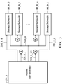
- FIG. 3 is a schematic diagram depicting connections between one access sub-interface and multiple storage sub-units according to an embodiment of the invention.
- FIG. 4 is a block diagram illustrating a test writer according to an embodiment of the invention.
- FIG. 5A is a schematic diagram of an output result of a CRC encoder according to an embodiment of the invention.
- FIG. 5B is a schematic diagram of an output result of a scrambler according to an embodiment of the invention.
- FIG. 5C is a schematic diagram of an output result of an ECC encoder according to an embodiment of the invention.
- FIG. 6 is a block diagram of a test reader according to an embodiment of the invention.
- FIG. 7A is a schematic diagram of a test data read by an ECC decoder according to an embodiment of the invention.
- FIG. 7B is a schematic diagram of a test data read by a de-scrambler according to an embodiment of the invention.
- FIG. 7C is a schematic diagram of a test data read by a CRC decoder according to an embodiment of the invention.
- FIG. 8 is a flowchart illustrating a method for testing a storage unit according to an embodiment of the invention.
- FIG. 1 is the system architecture of a flash memory according to an embodiment of the invention.
- the system architecture 10 of the flash memory contains a processing unit 110 .
- the processing unit 110 can be implemented in numerous ways, such as with dedicated hardware, or with general-purpose hardware (e.g., a single processor, multiple processors or graphics processing units capable of parallel computations, etc.) that is programmed using microcode or software instructions to perform the functions recited herein.
- the processing unit 110 may contain one or more ALUs (Arithmetic and Logic Units) and bit shifters.
- the ALU is responsible for performing boolean operations (such as, AND, OR, NOT, NAND, NOR, XOR, XNOR, etc.) and also for performing integer addition and subtraction.
- the bit shifter is responsible for bitwise shifts and rotations.
- the system architecture 10 uses several electrical signals for coordinating commands and data transfer between the processing unit 110 and the storage unit 180 , including data lines, a clock signal and control lines.
- the data lines are employed to transfer commands, addresses and data to be written and read.
- the control lines are utilized to issue control signals, such as CE (Chip Enable), ALE (Address Latch Enable), CLE (Command Latch Enable), WE (Write Enable), etc.
- CE Chip Enable
- ALE Address Latch Enable
- CLE Common Latch Enable
- WE Write Enable
- the access interface 170 may communicate with the storage unit 180 using a SDR (Single Data Rate) protocol or a DDR (Double Data Rate) protocol, such as ONFI (open NAND flash interface), DDR toggle, or others.
- SDR Single Data Rate
- DDR Double Data Rate
- the processing unit 110 may communicate with the host device 160 through an access interface 150 using a standard protocol, such as USB (Universal Serial Bus), ATA (Advanced Technology Attachment), SATA (Serial ATA), PCI-E (Peripheral Component Interconnect Express) or others.
- a standard protocol such as USB (Universal Serial Bus), ATA (Advanced Technology Attachment), SATA (Serial ATA), PCI-E (Peripheral Component Interconnect Express) or others.
- the storage unit 180 may contain multiple storage sub-units and each storage sub-unit may be practiced in a single die and use a respective access sub-interface to communicate with the processing unit 110 .
- FIG. 2 is a schematic diagram illustrating interfaces to storage units of a flash storage according to an embodiment of the invention.
- the flash memory system 10 may contain j+1 access sub-interfaces 170 _ 0 to 170 _ j , where the access sub-interfaces may be referred to as channels, and each access sub-interface connects to i+1 storage sub-units. That is, i+1 storage sub-units may share the same access sub-interface.
- the flash memory 10 has 16 storage sub-units 180 _ 0 _ 0 to 180 _ j _i in total.
- the processing unit 110 may direct one of the access sub-interfaces 170 _ 0 to 170 _ j to program data into the designated storage sub-unit.
- Each storage sub-unit has an independent CE control signal. That is, it is required to enable a corresponding CE control signal when attempting to perform a data write into a designated storage sub-unit via an associated access sub-interface.
- FIG. 3 is a schematic diagram depicting connections between one access sub-interface and multiple storage sub-units according to an embodiment of the invention.
- the processing unit 110 through the access sub-interface 170 _ 0 , may use independent CE control signals 320 _ 0 _ 0 to 320 _ 0 _ i to select one of the connected storage sub-units 180 _ 0 _ 0 and 180 _ 0 _ i , and then program data into the designated location of the selected storage sub-unit via the shared data line 310 _ 0 .
- the processing unit 110 may use one of two modes to direct the access interface 170 to program data: One is normal write; and the other is test write.
- a factory may perform test writes in mass production for labeling all bad blocks of the storage unit 180 . Normal writes are performed after the flash memory system 10 leaves the factory.
- the processing unit 110 enters the normal write mode. Specifically, in the normal write mode, the processing unit 110 issues a control signal CTRL to direct a data dispatcher 120 to send data DAT 1 to the access interface 170 and issues a command CMD 2 to direct the access interface 170 to program the data DAT 1 into a designated address of the storage unit 180 .
- the processing unit 110 When a write command CMD 1 issued by the host device 160 instructs a test write, the processing unit 110 enters the test write mode. Specifically, in the test write mode, the processing unit 110 issues a control signal CTRL to direct the data dispatcher 120 to send data DAT 1 to a test writer 131 .
- the test writer 131 generates test patterns DAT 2 according to the data DAT 1 and dummy data output from a dummy-data generator 140 . Exemplary generation of the test patterns DAT 2 will be described in the following paragraphs.
- the processing unit 110 issues a command CMD 2 to direct the access interface 170 to read one or more test patterns DAT 2 from the test writer 131 and program the test pattern(s) DAT 2 into a designated PBA (physical block address) of the storage unit 180 .
- the data dispatcher 120 may be practiced in a de-multiplexer to couple the data line of the access interface 150 to either the test writer 131 or the access interface 170 according to the control signal CTRL.
- the processing unit 110 further issues a command CMD 3 to direct the access interface 170 to read test pattern(s) DAT 3 from the designated PBA and output the test pattern(s) DAT 3 to a test reader 133 .
- the test reader 133 verifies each bit of the test pattern(s) DAT 3 for determining whether the read data DAT 3 is correct or has error bit(s) and outputs a test result RT′ to the processing unit 110 .
- the processing unit 110 replies a test result RT to the host device 160 via the access interface 150 .
- FIG. 4 is a block diagram illustrating a test writer according to an embodiment of the invention.
- a test writer 131 contains a CRC (Cyclic Redundancy Check) encoder 410 , a scrambler 430 and an ECC (Error-Correcting Code) encoder 450 .
- the CRC encoder 410 may receive metadata DAT 1 through the data dispatcher 120 and receive dummy data DUM from the dummy-data generator 140 .
- the CRC encoder 410 encodes the dummy data DUM and the metadata DAT 1 by adding a fixed-length parity for the purpose of error detection and outputs a result DAT 1 ′ to the scrambler 430 .
- the metadata DAT 1 may be a PBA for a test write.
- FIG. 5A is a schematic diagram of an output result of a CRC encoder according to an embodiment of the invention.
- An output result DAT 1 ′ contains dummy data 510 , metadata 530 and a parity 550 .
- the scrambler 430 may use a well-known algorithm to transform the dummy data DUM to random and distinct scrambled data DUM′ to ensure DC balance and outputs a result DAT′′ to the ECC encoder 450 .
- FIG. 5B is a schematic diagram of an output result of a scrambler according to an embodiment of the invention.
- An output result DAT 1 ′′ contains scrambled data 510 ′, the metadata 530 and the parity 550 .
- the ECC encoder 450 encodes the scrambled data DUM′, the metadata DAT 1 and the parity in a redundant way by using an ECC.
- FIG. 5C is a schematic diagram of an output result of an ECC encoder according to an embodiment of the invention.
- An output result DAT 2 contains scrambled data 510 ′, the metadata 530 , the parity 550 and the ECC 570 .
- FIG. 6 is a block diagram of a test reader according to an embodiment of the invention.
- a test reader 133 contains an ECC decoder 610 , a de-scrambler 630 and a CRC decoder 650 .
- the ECC decoder 610 reads the test data DAT 3 from the designated PBA via the access interface 170 .
- FIG. 7A is a schematic diagram of a test data read by an ECC decoder according to an embodiment of the invention.
- Input data DAT 3 may be segmented into parts including scrambled data 710 , metadata 730 , a parity 750 and an ECC 770 .
- An ECC decoder 610 uses the ECC 770 to determine whether the scrambled data 710 , the metadata 730 and the parity 750 have any errors. When no error has been inspected, the ECC decoder 610 transmits a message RT 1 to the processing unit 110 to indicate that the test data DAT 3 has passed the ECC examination. When an error has been inspected, the ECC decoder 610 attempts to fix the errors in the test data DAT 3 . When the errors have been fixed successfully, the ECC decoder 610 transmits a message RT 1 to the processing unit 110 to indicate that the test data DAT 3 has been successfully fixed.
- FIG. 7B is a schematic diagram of a test data read by a de-scrambler according to an embodiment of the invention.
- Input data DAT 3 ′ may be segmented into parts including the (error-corrected) scrambled data 710 ′, metadata 730 ′ and parity 750 ′.
- the de-scrambler 630 may use a well-known algorithm to de-scramble the (error-corrected) scrambled data 710 ′ and outputs the de-scrambled data DAT 3 ′′ to the CRC decoder 650 .
- FIG. 7C is a schematic diagram of test data read by a CRC decoder according to an embodiment of the invention. Input data DAT 3 ′′ may be segmented into parts including the de-scrambled data 710 ′′, the (error-corrected) metadata 730 ′ and parity 750 ′.
- the CRC decoder 650 uses the (error-corrected) parity 750 ′ to determine whether the de-scrambled data 710 ′′ and the (error-corrected) metadata 730 ′ have any errors.
- the CRC decoder 650 transmits a message RT 2 to the processing unit 110 to indicate that the test data DAT 3 has passed the CRC examination.
- the CRC decoder 650 transmits a message RT 2 to the processing unit 110 to indicate that the test data DAT 3 hasn't passed the CRC examination.
- the processing unit 110 generates an integrated message RT according to the messages RT 1 and RT 2 and replies the integrated message RT to the host device 160 .
- the message RT indicates that the programming of test data into the designated PBA is successful or has failed. In another example, the message RT indicates that test data being programmed into the designated PBA has passed the ECC and CRC examination. In still another example, the message RT indicates that test data being programmed into the designated PBA has passed the ECC examination but failed to pass the CRC examination.
- the host device 160 determines whether a block corresponding to the designated PBA of the storage unit 180 is labeled as a bad block according to the received message RT. For example, when receiving a message RT indicating that the programming of test data into the designated PBA has failed, the host device 160 labels a block corresponding to the designated PBA of the storage unit 180 as a bad block. Since the flash memory system 10 incorporates the functionalities of the test writer 131 and the test reader 133 , the host device 130 needs to transmit only PBAs to the flash memory system 10 to complete complicated test writes, resulting in the reduction of test cost.
- FIG. 8 is a flowchart illustrating a method for testing a storage unit according to an embodiment of the invention. The method is performed by the processing unit 110 when loading and executing relevant micro-codes or software instructions. After receiving a test write command from the host device 160 through the access interface 150 (step S 810 ), the processing unit 110 issues a control signal CTRL to direct the data dispatcher 120 to send data DAT 1 (including a PBA) from the host device 160 to the test writer 131 (step S 820 ).
- data DAT 1 including a PBA
- the processing unit 110 issues a command CMD 2 to direct the access interface 170 to read one or more test patterns DAT 2 from the test writer 131 and program the test pattern(s) DAT 2 into a designated PBA of the storage unit 180 (step S 830 ), and next, issues a command CMD 3 to direct the access interface 170 to read test pattern(s) DAT 3 from the designated PBA and output the test pattern(s) DAT 3 to the test reader 133 (step S 840 ).
- the processing unit 110 receives a test result RT′ from the test reader 133 (step S 850 ), generates a test message RT according to the test result RT′ and replies with the test message RT to the host device 160 (step S 860 ).
- FIG. 8 includes a number of operations that appear to occur in a specific order, it should be apparent that these processes can include more or fewer operations, which can be executed serially or in parallel (e.g., using parallel processors or a multi-threading environment).
Landscapes
- Engineering & Computer Science (AREA)
- Theoretical Computer Science (AREA)
- General Engineering & Computer Science (AREA)
- Physics & Mathematics (AREA)
- Quality & Reliability (AREA)
- General Physics & Mathematics (AREA)
- Computer Hardware Design (AREA)
- Techniques For Improving Reliability Of Storages (AREA)
- Probability & Statistics with Applications (AREA)
Abstract
Description
Claims (20)
Applications Claiming Priority (3)
| Application Number | Priority Date | Filing Date | Title |
|---|---|---|---|
| CN201610879580 | 2016-10-08 | ||
| CN201610879580.5A CN107918571B (en) | 2016-10-08 | 2016-10-08 | Method for testing storage unit and device using same |
| CN201610879580.5 | 2016-10-08 |
Publications (2)
| Publication Number | Publication Date |
|---|---|
| US20180102182A1 US20180102182A1 (en) | 2018-04-12 |
| US10636506B2 true US10636506B2 (en) | 2020-04-28 |
Family
ID=61829136
Family Applications (1)
| Application Number | Title | Priority Date | Filing Date |
|---|---|---|---|
| US15/663,958 Active 2037-10-13 US10636506B2 (en) | 2016-10-08 | 2017-07-31 | Methods for testing a storage unit and apparatuses using the same |
Country Status (3)
| Country | Link |
|---|---|
| US (1) | US10636506B2 (en) |
| CN (1) | CN107918571B (en) |
| TW (1) | TWI676991B (en) |
Families Citing this family (8)
| Publication number | Priority date | Publication date | Assignee | Title |
|---|---|---|---|---|
| TWI658364B (en) * | 2018-03-20 | 2019-05-01 | 慧榮科技股份有限公司 | Method for accessing flash memory module and associated flash memory controller and electronic device |
| CN115509961A (en) * | 2018-06-25 | 2022-12-23 | 慧荣科技股份有限公司 | Apparatus and method for generating entity storage comparison table |
| KR102599188B1 (en) * | 2018-11-09 | 2023-11-08 | 삼성전자주식회사 | Storage device using host memory and operating method thereof |
| US11081203B2 (en) * | 2019-11-14 | 2021-08-03 | Micron Technology, Inc. | Leakage source detection by scanning access lines |
| JP7438859B2 (en) * | 2020-06-17 | 2024-02-27 | キオクシア株式会社 | Memory systems and methods |
| JP2023060606A (en) * | 2021-10-18 | 2023-04-28 | キオクシア株式会社 | Semiconductor integrated circuit and memory system |
| CN114999558B (en) * | 2022-08-03 | 2022-11-29 | 合肥康芯威存储技术有限公司 | Method and system for testing memory chip |
| CN117155788B (en) * | 2023-10-30 | 2024-01-26 | 博测通讯科技(上海)有限公司 | SAR testing system, cloud platform and method for electronic product |
Citations (22)
| Publication number | Priority date | Publication date | Assignee | Title |
|---|---|---|---|---|
| US5875293A (en) * | 1995-08-08 | 1999-02-23 | Dell Usa, L.P. | System level functional testing through one or more I/O ports of an assembled computer system |
| US20060200708A1 (en) * | 2002-03-18 | 2006-09-07 | Paul Gentieu | System and method for network error rate testing |
| US20060220928A1 (en) * | 2005-03-31 | 2006-10-05 | Fujitsu Limited | Encoder and decoder |
| US20060256875A1 (en) * | 2002-07-10 | 2006-11-16 | Mcclellan Brett A | Communication system and encoding method having low overhead |
| US20080052564A1 (en) | 2006-08-25 | 2008-02-28 | Samsung Electronics Co., Ltd. | Error correction circuit and method, and semiconductor memory device including the circuit |
| US20090183032A1 (en) * | 2008-01-11 | 2009-07-16 | Arm Limited | Data processing apparatus and method for testing stability of memory cells in a memory device |
| US7729384B1 (en) * | 2005-11-01 | 2010-06-01 | Metanoia Technologies, Inc. | Multiple channel digital subscriber line framer/deframer system and method |
| US20130080854A1 (en) | 2011-09-23 | 2013-03-28 | International Business Machines Corporation | Address error detection |
| US8429426B2 (en) * | 2007-10-30 | 2013-04-23 | Sandisk Il Ltd. | Secure pipeline manager |
| US20130111301A1 (en) * | 2011-11-02 | 2013-05-02 | Phison Electronics Corp. | Block management method, memory controller and memory storage device thereof |
| US20130124932A1 (en) | 2011-11-14 | 2013-05-16 | Lsi Corporation | Solid-State Disk Manufacturing Self Test |
| TWI401691B (en) | 2009-03-20 | 2013-07-11 | Phison Electronics Corp | Controller having flash memory testing functions, storage system and testing method thereof |
| US20140129883A1 (en) | 2012-11-05 | 2014-05-08 | Freescale Semiconductor, Inc. | Hardware-based memory initialization |
| US20140359395A1 (en) | 2013-05-29 | 2014-12-04 | Lsi Corporation | Protection of data in memory |
| US20150052416A1 (en) | 2013-08-16 | 2015-02-19 | Seagate Technology Llc | Determining Data Retention Time in a Solid-State Non-Volatile Memory |
| US20150082104A1 (en) * | 2013-02-14 | 2015-03-19 | Micron Technology, Inc. | Autorecovery after manufacturing/system integration |
| US20150154943A1 (en) * | 2013-12-03 | 2015-06-04 | Samsung Electronics Co., Ltd. | Timing Controller, Source Driver, and Display Driver Integrated Circuit Having Improved Test Efficiency and Method of Operating Display Driving Circuit |
| US20150242657A1 (en) * | 2014-02-27 | 2015-08-27 | Jisoo Kim | Self-encrypting drive and user device including the same |
| US20150280742A1 (en) * | 2014-03-28 | 2015-10-01 | National Taiwan University | Caching method and data storage system capable of prolonging service lifetime of a cache memory |
| US20160062908A1 (en) * | 2014-09-02 | 2016-03-03 | Silicon Motion, Inc. | Methods for Maintaining a Storage Mapping Table and Apparatuses using the Same |
| US20160124826A1 (en) * | 2014-10-31 | 2016-05-05 | Megachips Corporation | Semiconductor device and method for testing reliability of semiconductor device |
| US20160277041A1 (en) * | 2015-03-17 | 2016-09-22 | Sk Hynix Memory Solutions Inc. | Incremental llr generation for flash memories |
Family Cites Families (5)
| Publication number | Priority date | Publication date | Assignee | Title |
|---|---|---|---|---|
| JP4074029B2 (en) * | 1999-06-28 | 2008-04-09 | 株式会社東芝 | Flash memory |
| KR100645043B1 (en) * | 2004-09-08 | 2006-11-10 | 삼성전자주식회사 | Nonvolatile memory device with test buffer and test method for the same |
| TWI415130B (en) * | 2009-06-02 | 2013-11-11 | Silicon Motion Inc | Flash memory controller and method for accessing a flash memory |
| TWI527048B (en) * | 2013-11-29 | 2016-03-21 | 慧榮科技股份有限公司 | Error correction code unit, self-test method and associated controller applied to flash memory device |
| TWI512609B (en) * | 2014-09-05 | 2015-12-11 | Silicon Motion Inc | Methods for scheduling read commands and apparatuses using the same |
-
2016
- 2016-10-08 CN CN201610879580.5A patent/CN107918571B/en active Active
- 2016-11-16 TW TW105137393A patent/TWI676991B/en active
-
2017
- 2017-07-31 US US15/663,958 patent/US10636506B2/en active Active
Patent Citations (22)
| Publication number | Priority date | Publication date | Assignee | Title |
|---|---|---|---|---|
| US5875293A (en) * | 1995-08-08 | 1999-02-23 | Dell Usa, L.P. | System level functional testing through one or more I/O ports of an assembled computer system |
| US20060200708A1 (en) * | 2002-03-18 | 2006-09-07 | Paul Gentieu | System and method for network error rate testing |
| US20060256875A1 (en) * | 2002-07-10 | 2006-11-16 | Mcclellan Brett A | Communication system and encoding method having low overhead |
| US20060220928A1 (en) * | 2005-03-31 | 2006-10-05 | Fujitsu Limited | Encoder and decoder |
| US7729384B1 (en) * | 2005-11-01 | 2010-06-01 | Metanoia Technologies, Inc. | Multiple channel digital subscriber line framer/deframer system and method |
| US20080052564A1 (en) | 2006-08-25 | 2008-02-28 | Samsung Electronics Co., Ltd. | Error correction circuit and method, and semiconductor memory device including the circuit |
| US8429426B2 (en) * | 2007-10-30 | 2013-04-23 | Sandisk Il Ltd. | Secure pipeline manager |
| US20090183032A1 (en) * | 2008-01-11 | 2009-07-16 | Arm Limited | Data processing apparatus and method for testing stability of memory cells in a memory device |
| TWI401691B (en) | 2009-03-20 | 2013-07-11 | Phison Electronics Corp | Controller having flash memory testing functions, storage system and testing method thereof |
| US20130080854A1 (en) | 2011-09-23 | 2013-03-28 | International Business Machines Corporation | Address error detection |
| US20130111301A1 (en) * | 2011-11-02 | 2013-05-02 | Phison Electronics Corp. | Block management method, memory controller and memory storage device thereof |
| US20130124932A1 (en) | 2011-11-14 | 2013-05-16 | Lsi Corporation | Solid-State Disk Manufacturing Self Test |
| US20140129883A1 (en) | 2012-11-05 | 2014-05-08 | Freescale Semiconductor, Inc. | Hardware-based memory initialization |
| US20150082104A1 (en) * | 2013-02-14 | 2015-03-19 | Micron Technology, Inc. | Autorecovery after manufacturing/system integration |
| US20140359395A1 (en) | 2013-05-29 | 2014-12-04 | Lsi Corporation | Protection of data in memory |
| US20150052416A1 (en) | 2013-08-16 | 2015-02-19 | Seagate Technology Llc | Determining Data Retention Time in a Solid-State Non-Volatile Memory |
| US20150154943A1 (en) * | 2013-12-03 | 2015-06-04 | Samsung Electronics Co., Ltd. | Timing Controller, Source Driver, and Display Driver Integrated Circuit Having Improved Test Efficiency and Method of Operating Display Driving Circuit |
| US20150242657A1 (en) * | 2014-02-27 | 2015-08-27 | Jisoo Kim | Self-encrypting drive and user device including the same |
| US20150280742A1 (en) * | 2014-03-28 | 2015-10-01 | National Taiwan University | Caching method and data storage system capable of prolonging service lifetime of a cache memory |
| US20160062908A1 (en) * | 2014-09-02 | 2016-03-03 | Silicon Motion, Inc. | Methods for Maintaining a Storage Mapping Table and Apparatuses using the Same |
| US20160124826A1 (en) * | 2014-10-31 | 2016-05-05 | Megachips Corporation | Semiconductor device and method for testing reliability of semiconductor device |
| US20160277041A1 (en) * | 2015-03-17 | 2016-09-22 | Sk Hynix Memory Solutions Inc. | Incremental llr generation for flash memories |
Also Published As
| Publication number | Publication date |
|---|---|
| CN107918571B (en) | 2021-04-30 |
| TWI676991B (en) | 2019-11-11 |
| US20180102182A1 (en) | 2018-04-12 |
| CN107918571A (en) | 2018-04-17 |
| TW201814722A (en) | 2018-04-16 |
Similar Documents
| Publication | Publication Date | Title |
|---|---|---|
| US10636506B2 (en) | Methods for testing a storage unit and apparatuses using the same | |
| US8261140B2 (en) | Uninitialized memory detection using error correction codes and built-in self test | |
| US9513995B2 (en) | Methods for accessing a storage unit of a flash memory and apparatuses using the same | |
| KR20100082710A (en) | Data memory device and controller with interface error detection and handling logic | |
| JP2006195990A (en) | Semiconductor disk controller | |
| US10552262B2 (en) | Data programming for a data storage medium using horizontal and vertical error correction codes | |
| US10199108B2 (en) | Methods for read retries and apparatuses using the same | |
| TWI584291B (en) | Memory management method, memory control circuit unit and memory storage device | |
| US20150058537A1 (en) | Methods for Accessing a Storage Unit of a Flash Memory and Apparatuses using the Same | |
| US20160253239A1 (en) | Data storage device and operating method thereof | |
| US11651707B2 (en) | Method and apparatus for encrypting and decrypting user data | |
| US20090259916A1 (en) | Data accessing method, controller and storage system using the same | |
| US11514995B2 (en) | Memory sub-system self-testing operations | |
| US10861576B2 (en) | Nonvolatile memory device, operating method thereof and data storage device including the same | |
| US10338998B2 (en) | Methods for priority writes in an SSD (solid state disk) system and apparatuses using the same | |
| US10254994B2 (en) | Methods for migrating data to avoid read disturbance and apparatuses using the same | |
| KR20170133545A (en) | Semiconductor device and semiconductor system | |
| US9778864B2 (en) | Data storage device using non-sequential segment access and operating method thereof | |
| US20220035700A1 (en) | Detecting special handling metadata using address verification | |
| CN115203099A (en) | System including PIPE 5-to-PIPE 4 converter and method thereof | |
| US10204699B2 (en) | Methods for migrating data to avoid read disturbance and apparatuses using the same | |
| CN111796774A (en) | Memory control method, memory storage device and memory controller | |
| US11403038B2 (en) | Controller, a memory system including the controller, and method of operating the controller | |
| TWI807919B (en) | Data retry-read method, a memory storage device and a memory control circuit unit | |
| US20230315302A1 (en) | Complete And Fast Protection Against CID Conflict |
Legal Events
| Date | Code | Title | Description |
|---|---|---|---|
| AS | Assignment |
Owner name: SHANNON SYSTEMS LTD., CHINA Free format text: ASSIGNMENT OF ASSIGNORS INTEREST;ASSIGNOR:ZHOU, ZHEN;REEL/FRAME:043379/0212 Effective date: 20170717 |
|
| STPP | Information on status: patent application and granting procedure in general |
Free format text: RESPONSE TO NON-FINAL OFFICE ACTION ENTERED AND FORWARDED TO EXAMINER |
|
| STPP | Information on status: patent application and granting procedure in general |
Free format text: FINAL REJECTION MAILED |
|
| STPP | Information on status: patent application and granting procedure in general |
Free format text: ADVISORY ACTION MAILED |
|
| STPP | Information on status: patent application and granting procedure in general |
Free format text: DOCKETED NEW CASE - READY FOR EXAMINATION |
|
| STPP | Information on status: patent application and granting procedure in general |
Free format text: NON FINAL ACTION MAILED |
|
| STPP | Information on status: patent application and granting procedure in general |
Free format text: RESPONSE TO NON-FINAL OFFICE ACTION ENTERED AND FORWARDED TO EXAMINER |
|
| STPP | Information on status: patent application and granting procedure in general |
Free format text: NOTICE OF ALLOWANCE MAILED -- APPLICATION RECEIVED IN OFFICE OF PUBLICATIONS |
|
| STCF | Information on status: patent grant |
Free format text: PATENTED CASE |
|
| MAFP | Maintenance fee payment |
Free format text: PAYMENT OF MAINTENANCE FEE, 4TH YR, SMALL ENTITY (ORIGINAL EVENT CODE: M2551); ENTITY STATUS OF PATENT OWNER: SMALL ENTITY Year of fee payment: 4 |