US10615793B2 - Deformable input apparatus and electronic apparatus including key regions - Google Patents
Deformable input apparatus and electronic apparatus including key regions Download PDFInfo
- Publication number
- US10615793B2 US10615793B2 US14/777,776 US201414777776A US10615793B2 US 10615793 B2 US10615793 B2 US 10615793B2 US 201414777776 A US201414777776 A US 201414777776A US 10615793 B2 US10615793 B2 US 10615793B2
- Authority
- US
- United States
- Prior art keywords
- capacitive element
- electrode substrate
- key
- input
- key regions
- Prior art date
- Legal status (The legal status is an assumption and is not a legal conclusion. Google has not performed a legal analysis and makes no representation as to the accuracy of the status listed.)
- Expired - Fee Related, expires
Links
- 239000000758 substrate Substances 0.000 claims abstract description 157
- 230000008859 change Effects 0.000 claims abstract description 100
- 239000004020 conductor Substances 0.000 claims description 45
- 230000008878 coupling Effects 0.000 claims description 23
- 238000010168 coupling process Methods 0.000 claims description 23
- 238000005859 coupling reaction Methods 0.000 claims description 23
- 238000005516 engineering process Methods 0.000 abstract description 15
- 239000010410 layer Substances 0.000 description 59
- 238000001514 detection method Methods 0.000 description 46
- 239000000463 material Substances 0.000 description 46
- 238000005452 bending Methods 0.000 description 14
- 230000035945 sensitivity Effects 0.000 description 12
- 230000009471 action Effects 0.000 description 11
- 238000010586 diagram Methods 0.000 description 11
- 238000000034 method Methods 0.000 description 10
- 229910052751 metal Inorganic materials 0.000 description 8
- 239000002184 metal Substances 0.000 description 8
- 239000010408 film Substances 0.000 description 7
- 239000002985 plastic film Substances 0.000 description 7
- 239000011347 resin Substances 0.000 description 7
- 229920005989 resin Polymers 0.000 description 7
- 238000003825 pressing Methods 0.000 description 5
- 229920003207 poly(ethylene-2,6-naphthalate) Polymers 0.000 description 4
- 239000004417 polycarbonate Substances 0.000 description 4
- 239000011112 polyethylene naphthalate Substances 0.000 description 4
- 229920000139 polyethylene terephthalate Polymers 0.000 description 4
- 239000005020 polyethylene terephthalate Substances 0.000 description 4
- 238000003860 storage Methods 0.000 description 4
- 238000013459 approach Methods 0.000 description 3
- 238000004364 calculation method Methods 0.000 description 3
- 239000010949 copper Substances 0.000 description 3
- 238000010292 electrical insulation Methods 0.000 description 3
- 239000011888 foil Substances 0.000 description 3
- 238000009413 insulation Methods 0.000 description 3
- 230000002093 peripheral effect Effects 0.000 description 3
- 229920003229 poly(methyl methacrylate) Polymers 0.000 description 3
- 239000004926 polymethyl methacrylate Substances 0.000 description 3
- 238000007639 printing Methods 0.000 description 3
- 229910052782 aluminium Inorganic materials 0.000 description 2
- 229910052802 copper Inorganic materials 0.000 description 2
- 238000005530 etching Methods 0.000 description 2
- 230000006870 function Effects 0.000 description 2
- 239000011521 glass Substances 0.000 description 2
- 230000005484 gravity Effects 0.000 description 2
- 239000012994 photoredox catalyst Substances 0.000 description 2
- -1 polyethylene terephthalate Polymers 0.000 description 2
- RYGMFSIKBFXOCR-UHFFFAOYSA-N Copper Chemical compound [Cu] RYGMFSIKBFXOCR-UHFFFAOYSA-N 0.000 description 1
- 239000004593 Epoxy Substances 0.000 description 1
- 239000004642 Polyimide Substances 0.000 description 1
- 239000012790 adhesive layer Substances 0.000 description 1
- XAGFODPZIPBFFR-UHFFFAOYSA-N aluminium Chemical compound [Al] XAGFODPZIPBFFR-UHFFFAOYSA-N 0.000 description 1
- 239000011248 coating agent Substances 0.000 description 1
- 238000000576 coating method Methods 0.000 description 1
- 239000002131 composite material Substances 0.000 description 1
- 238000000151 deposition Methods 0.000 description 1
- 230000008021 deposition Effects 0.000 description 1
- 239000003989 dielectric material Substances 0.000 description 1
- 230000000694 effects Effects 0.000 description 1
- 239000013013 elastic material Substances 0.000 description 1
- 230000002349 favourable effect Effects 0.000 description 1
- 229920002457 flexible plastic Polymers 0.000 description 1
- 238000007647 flexography Methods 0.000 description 1
- 230000006872 improvement Effects 0.000 description 1
- 238000001746 injection moulding Methods 0.000 description 1
- 239000012774 insulation material Substances 0.000 description 1
- 238000010030 laminating Methods 0.000 description 1
- 238000004519 manufacturing process Methods 0.000 description 1
- 238000005192 partition Methods 0.000 description 1
- 229920006255 plastic film Polymers 0.000 description 1
- 229920000515 polycarbonate Polymers 0.000 description 1
- 229920001721 polyimide Polymers 0.000 description 1
- 230000004044 response Effects 0.000 description 1
- 238000007650 screen-printing Methods 0.000 description 1
- 229910052709 silver Inorganic materials 0.000 description 1
- 239000004332 silver Substances 0.000 description 1
- 238000004544 sputter deposition Methods 0.000 description 1
- 239000010409 thin film Substances 0.000 description 1
- 238000001721 transfer moulding Methods 0.000 description 1
Images


Classifications
-
- H—ELECTRICITY
- H03—ELECTRONIC CIRCUITRY
- H03K—PULSE TECHNIQUE
- H03K17/00—Electronic switching or gating, i.e. not by contact-making and –breaking
- H03K17/94—Electronic switching or gating, i.e. not by contact-making and –breaking characterised by the way in which the control signals are generated
- H03K17/96—Touch switches
- H03K17/962—Capacitive touch switches
- H03K17/9622—Capacitive touch switches using a plurality of detectors, e.g. keyboard
-
- H—ELECTRICITY
- H03—ELECTRONIC CIRCUITRY
- H03K—PULSE TECHNIQUE
- H03K17/00—Electronic switching or gating, i.e. not by contact-making and –breaking
- H03K17/94—Electronic switching or gating, i.e. not by contact-making and –breaking characterised by the way in which the control signals are generated
- H03K17/96—Touch switches
- H03K2017/9602—Touch switches characterised by the type or shape of the sensing electrodes
- H03K2017/9604—Touch switches characterised by the type or shape of the sensing electrodes characterised by the number of electrodes
- H03K2017/9615—Touch switches characterised by the type or shape of the sensing electrodes characterised by the number of electrodes using three electrodes per touch switch
-
- H—ELECTRICITY
- H03—ELECTRONIC CIRCUITRY
- H03K—PULSE TECHNIQUE
- H03K2217/00—Indexing scheme related to electronic switching or gating, i.e. not by contact-making or -breaking covered by H03K17/00
- H03K2217/94—Indexing scheme related to electronic switching or gating, i.e. not by contact-making or -breaking covered by H03K17/00 characterised by the way in which the control signal is generated
- H03K2217/96—Touch switches
- H03K2217/96062—Touch switches with tactile or haptic feedback
-
- H—ELECTRICITY
- H03—ELECTRONIC CIRCUITRY
- H03K—PULSE TECHNIQUE
- H03K2217/00—Indexing scheme related to electronic switching or gating, i.e. not by contact-making or -breaking covered by H03K17/00
- H03K2217/94—Indexing scheme related to electronic switching or gating, i.e. not by contact-making or -breaking covered by H03K17/00 characterised by the way in which the control signal is generated
- H03K2217/96—Touch switches
- H03K2217/9607—Capacitive touch switches
- H03K2217/960705—Safety of capacitive touch and proximity switches, e.g. increasing reliability, fail-safe
-
- H—ELECTRICITY
- H03—ELECTRONIC CIRCUITRY
- H03K—PULSE TECHNIQUE
- H03K2217/00—Indexing scheme related to electronic switching or gating, i.e. not by contact-making or -breaking covered by H03K17/00
- H03K2217/94—Indexing scheme related to electronic switching or gating, i.e. not by contact-making or -breaking covered by H03K17/00 characterised by the way in which the control signal is generated
- H03K2217/96—Touch switches
- H03K2217/9607—Capacitive touch switches
- H03K2217/960755—Constructional details of capacitive touch and proximity switches
- H03K2217/96077—Constructional details of capacitive touch and proximity switches comprising an electrode which is floating
-
- H—ELECTRICITY
- H03—ELECTRONIC CIRCUITRY
- H03K—PULSE TECHNIQUE
- H03K2217/00—Indexing scheme related to electronic switching or gating, i.e. not by contact-making or -breaking covered by H03K17/00
- H03K2217/94—Indexing scheme related to electronic switching or gating, i.e. not by contact-making or -breaking covered by H03K17/00 characterised by the way in which the control signal is generated
- H03K2217/96—Touch switches
- H03K2217/9607—Capacitive touch switches
- H03K2217/960755—Constructional details of capacitive touch and proximity switches
- H03K2217/960775—Emitter-receiver or "fringe" type detection, i.e. one or more field emitting electrodes and corresponding one or more receiving electrodes
Definitions
- the present technology relates to an input apparatus and an electronic apparatus that are capable of electrostatically detecting an input operation.
- Patent Document 1 discloses an input device in which a GUI component such as a software keyboard is displayed on a touch panel functioning as a display device and, by touching a displayed key, that key is displayed.
- Patent Document 1 Japanese Patent Application Laid-open No. 2012-146267
- an object of the present technology to provide an input apparatus and an electronic apparatus that are capable of providing the stroke feeling and click feeling while ensuring the operability of the key inputs.
- an input apparatus includes an electrode substrate and a first support.
- the operation member includes a plurality of key regions and is configured to be deformable.
- the electrode substrate includes a first capacitive element arranged opposed to each of the plurality of key regions and a second capacitive element arranged around the first capacitive element.
- the electrode substrate is capable of electrostatically detecting a change of a distance from each of the plurality of key regions.
- the first support includes a plurality of first structures and a first space.
- the plurality of first structures connect between the electrode substrate and the operation member.
- the first space is formed between the plurality of first structures and capable of changing the distance between each of the plurality of key regions and the electrode substrate according to an input operation.
- the input apparatus detects the input operation with respect to the key region, using a change of capacitance of the first and second capacitive elements based on a change of a distance by which each of the first and second capacitive elements is opposed to the key region. This enables the input operation to be performed in a state in which the finger or the like is placed on the operation member. Thus, it is possible to prevent the operability from being lowered. Further, each key region is supported on the electrode substrate via the first space formed between the plurality of first structures. Thus, predetermined stroke feeling and click feeling can be provided.
- the first capacitive elements and the second capacitive elements arranged around them are provided corresponding to each key region.
- a stable input operability irrespective of the input area and the input position can be provided.
- the first capacitive element may be arranged opposed to a center portion of each of the plurality of key regions.
- the second capacitive element is arranged opposed to a circumferential portion of each of the plurality of key regions.
- the electrode substrate may further include a limitation layer.
- the limitation layer is provided between the second capacitive element and the operation member and partially limits a thickness of the first space.
- the limitation layer is typically formed of a dielectric material. With this, the sensitivity of the second capacitive elements is enhanced and the variation of the operability due to the input area and the input position can be suppressed.
- the operation member may further include a conductor layer provided on a surface opposed to the electrode substrate.
- the input apparatus may further include a base substrate and a second support.
- the base substrate is provided opposed to the operation member while sandwiching the electrode substrate therebetween and includes a conductor layer on a surface opposed to the electrode substrate.
- the second support includes a plurality of second structures and a second space.
- the plurality of second structures connect between the electrode substrate and the base substrate and are respectively opposed to the plurality of first structures while sandwiching the electrode substrate therebetween.
- the second space is formed between the plurality of second structures and capable of changing the distance between the electrode substrate and the base substrate according to an input operation.
- the first support may further include a plurality of third structures.
- the plurality of third structures connect between the electrode substrate and the operation member and are arranged in the first space.
- a relative distance between each of the operation member and the conductor layer and the electrode substrate when pressed from above the operation member changes.
- the operation member may further include a coupling region that is supported by the plurality of first structures and couples the plurality of key regions to each other.
- the coupling region is formed to have flexural rigidity lower than that of the plurality of key regions.
- the plurality of key regions may be formed to have a thickness larger than that of the coupling region. With this, the flexural rigidity of the key region can be easily made higher than that in the coupling region.
- the input apparatus may further include a control unit.
- the control unit is electrically connected to the electrode substrate and configured to generate information on an input operation with respect to each of the plurality of key regions on the basis of outputs of the first capacitive element and the second capacitive element.
- the control unit may be configured to output an input signal if an amount of capacitance change of the first capacitive element is above a first threshold and an amount of capacitance change of the second capacitive element is above a second threshold smaller than the first threshold.
- control unit may be configured to output an input signal if a difference between an amount of capacitance change of the first capacitive element and an amount of capacitance change of the second capacitive element is above a predetermined threshold.
- control unit may be configured to output an input signal if an amount of capacitance change of the first capacitive element is above a first predetermined value and a time rate of change of capacitance of the first capacitive element is above a second predetermined value.
- An electronic apparatus includes an operation member, an electrode substrate, a first support, and a control unit.
- the operation member includes a plurality of key regions and is configured to be deformable.
- the electrode substrate includes a first capacitive element that is arranged opposed to each of the plurality of key regions, and a second capacitive element that is arranged around the first capacitive element.
- the electrode substrate is configured to be capable of electrostatically detecting the change of the distance from each of the plurality of key regions.
- the first support includes a plurality of first structures and a first space.
- the plurality of first structures connect between the electrode substrate and the operation member.
- the first space is formed between the plurality of first structures and configured to be capable of changing a distance between each of the plurality of key regions and the electrode substrate according to an input operation.
- the control unit is electrically connected to the electrode substrate and configured to generate information on an input operation with respect to each of the plurality of key regions on the basis of outputs of the first capacitive element and the second capacitive element.
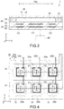
- FIG. 1 A schematic cross-sectional view of an input apparatus according to a first embodiment of the present technology.
- FIG. 2 A plan view of the input apparatus.
- FIG. 3 A main-part enlarged cross-sectional view of the input apparatus.
- FIG. 4 A main-part plan view showing the configuration of an electrode substrate in the input apparatus.
- FIG. 5 A main-part plan view of a first wiring board in the electrode substrate.
- FIG. 6 A main-part plan view of a second wiring board in the electrode substrate.
- FIG. 7 A cross-sectional view explaining a configuration example of the input apparatus.
- FIG. 8 A cross-sectional view explaining another configuration example of the input apparatus.
- FIG. 9 A diagram explaining the action of the input apparatus shown in FIG. 8 .
- FIG. 10 A diagram explaining the action of the input apparatus shown in FIG. 8 .
- FIG. 11 Main-part plan view and cross-sectional view showing the configuration of the input apparatus shown in FIG. 1 .
- FIG. 12 A main-part plan view showing a modified example of the configuration of the input apparatus.
- FIG. 13 Main-part plan view and cross-sectional view showing the configuration of the input apparatus shown in FIG. 1 .
- FIG. 14 Main-part plan view and cross-sectional view showing a modified example of the configuration of the input apparatus.
- FIG. 15 A diagram explaining the electrode shape of the input apparatus according to the comparison example and the action thereof.
- FIG. 16 A diagram explaining the electrode shape of the input apparatus shown in FIG. 1 and the action thereof.
- FIG. 17 A cross-sectional view showing another configuration example of the input apparatus shown in FIG. 1 .
- FIG. 18 A diagram explaining a detection method for an input operation using the input apparatus shown in FIG. 1 .
- FIG. 19 A diagram explaining the detection method for the input operation using the input apparatus shown in FIG. 1 .
- FIG. 20 Main-part plan view and cross-sectional view of an input apparatus according to a second embodiment of the present technology.
- FIG. 21 A cross-sectional view explaining the action of the input apparatus.
- FIG. 22 Main-part plan view and cross-sectional view showing a modified example of the input apparatus.
- FIG. 23 A main-part plan view showing a modified example of the electrode shape in the input apparatus shown in FIG. 1 .
- FIG. 24 A main-part plan view showing a modified example of the configuration of the capacitive element in the input apparatus shown in FIG. 1 .
- FIG. 1 is a schematic cross-sectional view of an input apparatus according to a first embodiment of the present technology.
- FIG. 2 is a plan view of the input apparatus.
- FIG. 3 is a main-part enlarged cross-sectional view of the input apparatus.
- an X-axis and a Y-axis show directions orthogonal to each other (in-plane direction of the input apparatus 1 ) and a Z-axis shows a direction orthogonal to the X-axis and Y-axis (thickness direction of the input apparatus 1 ).
- the input apparatus 1 includes an operation member 10 , an electrode substrate 20 , and a support 30 (first support).
- the input apparatus 1 is configured as a keyboard apparatus of an electronic apparatus such as a computer.
- the operation member 10 includes a plurality of key regions 10 a and is configured to be deformable.
- the electrode substrate 20 includes first capacitive elements C 1 arranged opposed to the plurality of key regions 10 a and second capacitive elements C 2 respectively arranged around the first capacitive elements C 1 .
- the electrode substrate 20 is configured to be capable of electrostatically detecting a change of a distance from each of the plurality of key regions 10 a.
- the support 30 includes a plurality of structures 31 (first structure) and a space 32 (first space).
- the plurality of structures 31 connect between the electrode substrate 20 and the operation member 10 .
- the first space 32 is formed among the plurality of structures 31 .
- the first space 32 is configured to be capable of changing a distance between each of the key regions 10 a and the electrode substrate 20 according to an input operation.
- the operation member 10 has a laminated structure of a base material 11 and a conductor layer 12 .
- the base material 11 is, for example, formed of a flexible insulation plastic sheet of PET (polyethylene terephthalate), PEN (polyethylene naphthalate), PMMA (polymethyl methacrylate), PC (polycarbonate), PI (polyimide), or the like.
- the thickness of the base material 11 is not particularly limited and is, for example, approximately several tens to several hundreds ⁇ m.
- the plurality of key regions 10 a are arrayed.
- the conductor layer 12 is provided on a back surface of the base material 11 , which is opposed to the electrode substrate 20 .
- the conductor layer 12 is formed of a metal foil or mesh material of Cu (copper), Al (aluminum), or the like.
- the conductor layer 12 is configured to be partially deformable toward the electrode substrate 20 when receiving input operations with respect to the plurality of key regions 10 a .
- the thickness of the conductor layer 12 is not particularly limited and is, for example, several tens nm to several tens ⁇ m.
- the conductor layer 12 is typically connected to a ground potential.
- the base material 11 and the conductor layer 12 may be formed of, for example, a composite sheet obtained by bonding a metal foil onto a surface of a resin sheet in advance.
- the base material 11 and the conductor layer 12 may be formed of, for example, a deposition film or sputtering film formed on the surface of the base material 11 .
- the base material 11 and the conductor layer 12 may be a coating film of a conductive paste or the like printed on the surface of the base material 11 .
- the conductor layer 12 may be omitted according to the specifications of the input apparatus 1 .
- Each of the key regions 10 a corresponds to a key top pressed and operated by a user and has shape and size depending on the type of the key.
- Each of the key regions 10 a is configured to be deformable toward the electrode substrate 20 according to a press operation (input operation) made by a finger of the user or an operation element such as a stylus.
- Key display may be performed on each of the key regions 10 a if necessary.
- the key display may display the type of the key, the position (outline) of the individual key, or the both.
- a suitable printing method for example, screen printing, flexography, or rotogravure can be adopted for the display.
- the base material 11 may be formed of a conductive material such as a metal. With this, the conductor layer 12 becomes unnecessary, which can make the operation member 10 thin. In this case, the base material 11 also functions as the conductor layer 12 and is, for example, connected to the ground potential.
- the electrode substrate 20 has a laminated structure of a first wiring board 21 and a second wiring board 22 .
- FIG. 4 is a main-part plan view showing the configuration of the electrode substrate 20 .
- FIG. 5 is a main-part plan view of the first wiring board 21 .
- FIG. 6 is a main-part plan view of the second wiring board 22 .
- the first wiring board 21 includes a first base material 21 s formed of an insulation plastic sheet and a plurality of first electrode wires 210 formed on the first base material 21 s.
- the plurality of first electrode wires 210 each include a first electrode section 211 and a second electrode section 212 .
- the first and second electrode sections 211 , 212 are arranged in a plurality of detection regions 21 a corresponding the plurality of key regions 10 a , respectively.
- the first electrode section 211 is located in a center portion of each detection region 21 a and the second electrode section 212 is located in a circumferential portion of each detection region 21 a.
- the first electrode wires 210 are formed connecting the detection regions 21 a in respective columns along an X-axis direction to one another in the X-axis direction.
- the first electrode section 211 and the second electrode section 212 are formed of independent electrode wires (first electrode wires 210 ), respectively.
- the second wiring board 22 includes a second base material 22 s formed of an insulation plastic sheet and a plurality of second electrode wires 220 formed on the second base material 22 s.
- the plurality of second electrode wires 220 each include a first electrode section 221 and a second electrode section 222 .
- the first and second electrode sections 221 , 222 are arranged in a plurality of detection regions 22 a corresponding to the plurality of key regions 10 a .
- the first electrode section 221 is located in a center portion of each detection region 22 a and the second electrode section 222 is located in a circumferential portion of each detection region 22 a.
- the second electrode wires 220 are formed connecting the detection regions 22 a in the respective columns along the X-axis direction to one another in a Y-axis direction.
- the first electrode section 221 and the second electrode section 222 are integrally connected to each other in each detection region 22 a.
- the first base material 21 s and the second base material 22 s are formed of an electrical insulation plastic sheet, glass substrate, glass epoxy substrate, or the like of PET, PEN, PC, PMMA, or the like.
- the thickness of the first base material 21 s and the second base material 22 s is not particularly limited and is, for example, several tens ⁇ m to several hundreds ⁇ m.
- the first base material 21 s and the second base material 22 s may be formed of a flexible sheet material or may be formed of an inflexible sheet material.
- the first electrode wires 210 and the second electrode wires 220 are respectively formed on the first base material 21 s and the second base material 22 s by, for example, etching of a metal foil of Al, Cu, or the like or printing of a metal paste of Ag (silver) or the like.
- the first wiring board 21 and the second wiring board 22 may be laminated such that the first and second electrode wires 210 , 220 are opposed to each other while sandwiching an adhesive layer (not shown) therebetween or may be laminated such that the first and second electrode wires 210 , 220 are opposed to each other while sandwiching at least either one of the first and second base materials 21 s , 22 s therebetween.
- the detection regions 21 a on the first wiring board 21 and the detection regions 22 a on the second wiring board 22 are opposed to each other in a Z-axis direction. In this manner, the detection regions 21 a on the first wiring board 21 and the detection regions 22 a on the second wiring board 22 form a plurality of detection regions 20 a of the electrode substrate 20 that are arranged opposed to the plurality of key regions 10 a.
- first electrode sections 211 of the first electrode wires 210 and the first electrode sections 221 of the second electrode wires 220 are opposed to each other in the Z-axis direction.
- first capacitive elements (capacitive sensors) C 1 of the electrode substrate 20 are formed.
- second electrode sections 212 of the first electrode wires 210 and the second electrode sections 222 of the second electrode wires 220 are opposed to each other in the Z-axis direction.
- second capacitive elements (capacitive sensors) C 2 of the electrode substrate 20 are formed.
- the first and second capacitive elements C 1 , C 2 have initial capacitances set in advance.
- the capacitances of the capacitive elements C 1 , C 2 change depending on distances from the key region 10 a (conductor layer 12 ) opposed to them.
- the electrode substrate 20 is electrically connected to a control unit 60 .
- the change of the distance between any of the key regions 10 a and the detection region 20 a opposed thereto is detected on the basis of the amount of capacitance change of the capacitive elements C 1 , C 2 .
- the electrode substrate 20 is configured to be capable of electrostatically detecting the change of the distance from each of the plurality of key regions 10 a.
- the first capacitive element C 1 is provided opposed to a center portion of each of the plurality of key regions 10 a and the second capacitive element C 2 is provided opposed to a circumferential portion of each of the plurality of key regions 10 a.
- the support 30 is provided between the operation member 10 and the electrode substrate 20 .
- the support 30 includes the plurality of structures 31 (first structure) and the space 32 (first space).
- the plurality of structures 31 connect between the electrode substrate 20 and the operation member 10 .
- the space 32 is formed among the plurality of structures 31 and configured to be capable of changing the distance between each of the plurality of key regions 10 a and the electrode substrate 20 according to an input operation.
- the support 30 further includes a base material 33 that supports the structures 31 .
- the base material 33 is formed of an electrical insulation plastic sheet of PET, PEN, PC, or the like.
- the base material 33 is laminated on the second wiring board 22 of the electrode substrate 20 .
- the thickness of the base material 33 is not particularly limited and is, for example, several ⁇ m to several hundreds ⁇ m.
- the plurality of structures 31 have the same height (e.g., several ⁇ m to several hundreds ⁇ m).
- the plurality of structures 31 connect between the electrode substrate 20 and the operation member 10 so as to partition the key regions 10 a of the operation member 10 (the detection regions 20 a of the electrode substrate 20 ).
- each of the structures 31 is formed of a material having relatively high rigidity.
- each of the structures 31 may be formed of an elastic material.
- Each of the structures 31 is formed of, for example, an electrical insulation resin material such as an ultraviolet curable resin.
- Each of the structures 31 is formed on the surface of the base material 33 by using a suitable method such as a transfer method.
- the space 32 is configured to be capable of partially elastically deforming the operation member 10 toward the electrode substrate 20 in each of the key regions 10 a .
- the space 32 is formed to mutually communicate with the plurality of key regions 10 a , it is not limited thereto.
- the space 32 may be independently provided in each of the key regions 10 a.
- the input apparatus 1 of this embodiment further includes the control unit 60 .
- the control unit 60 is electrically connected to the electrode substrate 20 and configured to generate, on the basis of outputs of the first capacitive element C 1 and the second capacitive element C 2 , information on an input operation with respect to each of the plurality of key regions 10 a.
- the control unit 60 is typically formed of a computer including a CPU/MPU, a memory, and the like.
- the control unit 60 may be formed of a single chip component or may be formed of a plurality of circuit components.
- the control unit 60 may be installed in the input apparatus 1 or may be installed in an apparatus main body (processing apparatus) connected to the input apparatus 1 .
- the control unit 60 is mounted on a flexible wiring board connected to the electrode substrate 20 .
- the control unit 60 may be integrally configured with a controller that controls the apparatus main body.
- the control unit 60 includes a storage unit and an arithmetic unit.
- the storage unit stores key layout information of the operation member 10 .
- the arithmetic unit executes input determination on the plurality of key regions 10 a on the basis of the key layout information stored in the storage unit and the outputs of the first and second capacitive elements C 1 , C 2 in each of the detection regions 20 a .
- the control unit 60 sets thresholds corresponding to the amount of capacitance change of the first and second capacitive elements C 1 , C 2 and performs a key input determination based on its level compared with the thresholds.
- control unit 60 is configured to output an input signal if the amount of capacitance change of the first capacitive element C 1 is above a first threshold and the amount of capacitance change of the second capacitive element C 2 is above a second threshold smaller than the first threshold.
- the control unit 60 is configured to output an input signal if a difference between the amount of capacitance change of the first capacitive element C 1 and the amount of capacitance change of the second capacitive element C 2 is above a predetermined threshold.
- the control unit 60 is configured to output an input signal if the amount of capacitance change of the first capacitive element C 1 is above a first predetermined value and a time rate of change of capacitance of the first capacitive element C 1 is above a second predetermined value.
- the storage unit may be configured to be capable of storing key layout information of a plurality of types of operation members including the plurality of key regions 10 a in different layouts. With this, it becomes possible to determine a suitable input operation also with respect to the plurality of operation members in different key layouts.
- the arithmetic unit is configured to generate a control signal varying depending on the amount of capacitance change of the first and second capacitive elements C 1 , C 2 in at least one detection region 20 a of the plurality of detection regions 20 a . With this, it becomes possible to perform not only on/off determination of the key region 10 a but also determination as to the presence/absence, operating force, or the like of a touch operation with respect to the key region 10 a.
- the arithmetic unit may be configured to generate a control signal if the amount of capacitance change of the first and second capacitive elements C 1 , C 2 in at least one detection region 20 a of the plurality of detection regions 20 a is equal to or larger than a predetermined value.
- the control signal is output to the apparatus main body (processing apparatus) only when an operation requiring control is performed.
- the amount of processing of signals in the apparatus main body can be reduced.
- the keyboard widely used as a key input apparatus enables a favorable and stable key input to be performed by using a depression (stroke) in pressing the key with a predetermined finger and a sense (click feeling) in pressing the key. For that reason, the keyboard is a widely used input apparatus.
- a mechanical keyboard 110 shown in FIG. 7 a plurality of substantially plate-like keys 101 movable in upper and lower directions and upper and lower conductive layers 102 , 103 below each of them are arranged.
- the mechanical keyboard 110 has a structure that the key 101 is pressed with a desired force to bring the upper and lower conductive layers 102 , 103 into contact with each other for obtaining a switch-on state.
- Such a structure imposes a limitation on fabrication of a thin keyboard.
- a thin keyboard or the like using a resistance change material between the upper and lower conductive layers has also been proposed.
- a key input apparatus with a touch panel is more and more popular.
- a screen keyboard is displayed on a part of the screen and character inputs are performed by touching the screen.
- the consistency of coordinates of the touch panel and a key region displayed on the screen is calculated, and if it is determined that the finger or the like has touched a predetermined key region, it is determined that a key input is performed.
- the input apparatus 1 of this embodiment has the following characteristics, for example.
- the input apparatus 1 of this embodiment functions to detect the change of the distance between the conductor layer 12 and the electrode substrate 20 provided on the back of the key region 10 a as the change of capacitance of the capacitive sensors (first and second capacitive elements C 1 , C 2 ). Therefore, with respect to a manipulation operation, in addition to the binary determination of on/off, it is possible to detect the change of the distance between the conductor layer 12 and the electrode substrate 20 on the basis of the change of capacitance of the capacitive sensors due to local deformation of the operation member 10 (key region 10 a ) depending on an operating force. With this, by setting thresholds corresponding to the amount of capacitance change, the key input determination can be performed based on its level compared with the thresholds.
- the operation sensitivity can be set by the values of the thresholds in the input apparatus 1 of this embodiment.
- an input apparatus can be formed of a single device having a plurality of performance operation load sensitivities. It means that, in addition to freely setting the operation load, even the key input apparatus can perform various types of detection such as coordinate detection using gravity center calculation and load-amount detection.
- the key input apparatus with the touch panel has to be operated by the finger separated therefrom as described above.
- a threshold corresponding to the amount of capacitance change depending on an operation load during operation is used, and hence, even when the finger touches the key region 10 a , the key input is not achieved as long as the load at this time is equal to or smaller than the set threshold. This allows the operator to perform an input operation while placing the finger on the key region 10 a.
- the input apparatus 1 of this embodiment includes the conductor layer 12 on the surface opposed to the electrode substrate 20 of the operation member 10 . Therefore, unlike a typical touch sensor that detects capacitive coupling between the finger and the capacitive sensor, the input apparatus 1 is capable of detecting an input operation based on the change of the distance between the conductor layer 12 and the electrode substrate 20 . Therefore, even when an input is performed by the distal edge of the nail or the finger wearing the glove, the conductor layer 12 causes desired deformation. Thus, an input operation by the use of the non-conductive operation element can be performed.
- the input apparatus 1 of this embodiment uses the thresholds of the amount of capacitance change for detecting an input operation, and hence can also partially use the gravity center calculation.
- This principle may be used to allow a single capacitive sensor (first and second capacitive elements C 1 , C 2 ) to be adapted for various types of key layouts.
- the layout of a general keyboard is slightly different between Japan and the United States, European countries, or the like.
- at least the sensor section (electrode substrate 20 ) can be commonly used. That is, a plurality of types of key tops constituting a desired key layout can use the common capacitive sensor. In this case, a key determination program complying with the types of key tops only needs to be prepared.
- the number of S may be larger than the number of necessary keys.
- two or more capacitive sensors may be assigned for a key larger than a typical key size, for example, a “Space” key, “Enter” key, or “Shift” key.
- a typical key size for example, a “Space” key, “Enter” key, or “Shift” key.
- the input apparatus 1 of this embodiment has the following advantages, for example.
- the operation member 10 , the electrode substrate 20 , and the support 30 are basically formed of a laminate of thin film materials, and hence the entire input apparatus 1 can be thin.
- the key determination is performed based on the change of the distance between the operation member 10 and the electrode substrate 20 , using the support 30 including the space 32 , and hence it is possible to identify the touch and switch.
- the threshold of the switch at this time can be freely set by changing parameters of the program, and hence the switch load sensitivity of the input apparatus can be easily changed.
- customizing, for example, changing the load sensitivity of a particular key can be easily performed.
- the capacitive sensors can be arranged according to the key layout.
- the common electrode substrate 20 can be used by selecting a program.
- the key input instruction is carried out when the amount of capacitance change equivalent to the key input is detected.
- the amount of capacitance change equivalent to the key input is detected.
- the data on the minute change of capacitance for example, it is possible to display information on a key as a press target on the screen, issue sound immediately before the key input, or change the size of the display. With this, a new usability can be realized.
- the operation surface of the keys 101 is moved in a direction substantially parallel to a press direction substantially without bending deformation in response to an operating force.
- the key operation surface is supported by an elastic body 104 having a predetermined spring constant, and hence the amount of movement of the key 101 depends on a relationship between the load during operation and the spring constant supporting the key operation surface.
- the variation of the amount of movement due to the position in the key region and the area is designed to be reduced.
- the key operation surface itself is also formed of a thin member (operation member 10 ). Therefore, with respect to the input apparatus such as the general keyboard, the key operation surface easily causes the bending deformation due to the operation load as shown in FIG. 8 . Therefore, as each shown in the upper, middle, and lower sections of FIG. 9 , the bending state largely varies depending on the operation position and operation area. Consequently, a variation of the amount of movement of the key operation surface easily occurs.
- the key determination is performed based on the level of the amount of capacitance change due to the amount of movement of the key operation surface, and hence the variation of the amount of movement of the key operation surface directly leads to the variation of the key determination.
- the key when the center portion of the key is pressed, the key is turned on with a small operating force. Meanwhile, when a portion near the corner of the key is pressed, a larger operation load is required. Due to such a variation, various inconveniences can occur. For example, it can be difficult to turn on the key in some key press positions during input. Further, the key can be unintentionally turned on while a motion of searching for a key in touch typing is performed. Thus, it is difficult to optimize the key determination.
- Countermeasures for the operation member 10 , the electrode substrate 20 , and the control unit 60 are carried out.
- Countermeasure Examples ⁇ 1> to ⁇ 4> below may be separately adopted or a combination of two or more countermeasure examples may be adopted.
- ⁇ 2> Provide a plurality of capacitance detection sensors and arrange them by separating the capacitive sensors into a portion with a large bending deformation amount and a portion with a small bending deformation amount.
- ⁇ 3> Arrange the plurality of capacitive sensors in a single key area and determine the switch-on in view of a predetermined calculation of a value detected by each of the capacitive sensors.
- ⁇ 4> Determine the switch-on by adding a determination criteria of a capacitance change speed associated with a key press speed.
- FIG. 10 shows a detection example of a key operation state.
- the change of capacitance when a conductor such as a finger F approaches the capacitive sensor (electrode substrate 20 ) is detected.
- the change of capacitance when the conductor layer 12 of a key operation film pressed by the finger F approaches the capacitive sensor (electrode substrate 20 ) is detected.
- the change of capacitance when the finger F and the mesh conductor layer 12 approach the capacitive sensor (electrode substrate 20 ) is detected.
- the upper section and the lower section of FIG. 11 are a main-part plan view of the key operation surface and a cross-sectional view thereof, respectively.
- the support surface of the key operation surface (operation member 10 ) is configured to be larger than the key region 10 a . That is, the plurality of structures 31 of the support 30 are located outside the key region 10 a . With this, the difference of the bending deformation amount between the center portion and the circumferential portion of the key region 10 a during key operation can be reduced. Therefore, it is possible to suppress the variation of the detection sensitivity and the erroneous detection due to the variation of the key input position.
- suitable display may be performed on the key region 10 a .
- the structure 31 may be configured to be divided as shown in FIG. 12 .
- FIGS. 13 and 14 each are a schematic diagram showing a modified example of the configuration of the operation member 10 .
- the upper sections of FIGS. 13 and 14 are main-part plan views of the key operation surface.
- the lower sections of FIGS. 13 and 14 are cross-sectional views thereof.
- the flexural rigidity of the key region is configured to be higher than the rigidity of the outer peripheral portion of the key region.
- the operation member 10 further includes coupling regions 13 that are supported by the plurality of structures 31 and couple the plurality of key regions 10 a to one another.
- the coupling regions 13 are set to have flexural rigidity lower than that of the plurality of key regions.
- the operation member 10 is configured such that the thickness of the key region 10 a is larger than the thickness of the outer peripheral portion (coupling region 13 ) of the key region 10 a .
- the individual key regions 10 a are formed protruding from the key operation surface, and hence the user can touch-type. Thus, it is possible to further improve the operability.
- Examples of the method of providing the key operation surface with a desired step include a method of freely adding a resin on the key operation surface by printing, a method using transfer molding a UV resin, a method of providing a film with concavo-convex portions by thermally pressing a desired die on a film, and a method using injection molding.
- the operation member 10 is formed of a metal sheet, desired concavo-convex portions can be formed by pressing metal, etching metal, or the like.
- the operation member 10 is configured such that the Young's modulus of the key region 10 a is larger than the Young's modulus of the outer peripheral portion (coupling region 13 ) of the key region 10 a . Also with this configuration, it is possible to reduce the amount of bending of the key region 10 a with respect to the key operation load and make the movement of the key region 10 a toward the electrode substrate 20 closer to the parallel movement.
- the arbitrary material layers are laminated on the predetermined regions in the surface opposed to the electrode substrate 20 of the operation member 10 , which are not supported by the structures 31 .
- the configuration is not limited thereto.
- the material layers may be laminated directly under at least the individual key regions 10 a . Further, the same actions can be obtained also by making certain regions supported by the structure 31 partially thin instead of laminating the other material layers.
- the detection method for the input operation in this embodiment is detection of the capacitance change in the electrode substrate 20 as described above.
- the capacitance change due to the deformation when the key is operated is, strictly speaking, a capacitance change due to the change of the distance of a conductive surface (conductor layer 12 ) that influences the capacitance of the sensor when the key is operated.
- the basic stance for the electrode arrangement in this embodiment is as follows.
- a predetermined determination criteria is added using data on the change of capacitance of the sensor electrodes arranged as in 1 above.
- the first and second capacitive elements C 1 , C 2 are arranged by separating the capacitive sensors in the detection regions 20 a of the electrode substrate 20 into a portion with a large bending deformation amount and a portion with a small bending deformation amount of the key region 10 a .
- the actions of this embodiment will be described as compared with different electrode arrangement examples.
- FIG. 15 an electrode arrangement example in which, in the individual detection region 20 a (key region 10 a ), two capacitive sensors C 10 , C 20 are separated and arranged in the left and right is assumed.
- the amount of capacitance change of the capacitive sensors C 10 , C 20 is larger in the case where the center portion of the key region 10 a is pressed by the ball of the finger F as shown on the middle right side of FIG. 15 in comparison with the case where the center portion of the key region 10 a is pressed by the distal edge of the nail of the finger F.
- the two capacitive sensors C 1 , C 2 are separated and arranged in the center portion and the circumferential portion of the individual detection region 20 a (key region 10 a ). Also in this case, the same as the above-mentioned example is obtained. That is, as compared with the case where the center portion of the key region 10 a is pressed by the distal edge of the nail of the finger F as shown on the middle left side of FIG. 16 , the amount of capacitance change of the capacitive sensors C 1 , C 2 is larger in the case where the center portion of the key region 10 a is pressed by the ball of the finger F as shown on the middle right side of FIG. 16 .
- the amount of capacitance change of the capacitive sensor C 2 is smaller in the case where the circumferential portion of the key region 10 a is pressed by the distal edge of the nail of the finger F as shown on the lower right side of FIG. 16 . This is based on a difference of the key input position.
- the variation of the amount of capacitance change due to the difference of the area and the difference of the position is smaller than that in the comparison example ( FIG. 15 ) and the absolute value of the amount of capacitance change due to the difference of the input position is larger. It can be seen from this that, according to this embodiment, the variation of the detection sensitivity and the erroneous detection due to the input area and the position can be suppressed.
- the change of capacitance of the capacitive sensor C 1 located in the key center portion occurs and the change of capacitance of the capacitive sensor C 2 located outside is smaller.
- the change of capacitance of the capacitive sensor C 1 is, of course, larger and at the same time the change of capacitance of the capacitive sensor C 2 is also larger. Using such characteristics of the change of capacitance, the following key determination method becomes possible.
- Determination Criteria 1 if ⁇ C 1 is larger than the predetermined threshold (S 00 ), the switch-on is determined.
- Determination Criteria 2 if the difference between ⁇ C 1 and ⁇ C 2 is above the predetermined threshold, the switch-on is determined.
- the fluctuation due to the area is suppressed using the characteristics that ⁇ C 1 easily fluctuates depending on the operation area and ⁇ C 2 also increases when the operation area increases.
- the capacitive sensors C 2 arranged around the capacitive sensor C 1 are located in the region with a small amount of deformation of the key film. Therefore, the amount of capacitance change ⁇ C 2 of the capacitive sensor C 2 when the center portion of the key region 10 a is operated is small. In view of this, by configuring the electrode substrate as follows, ⁇ C 2 during key operation may be ensured.
- FIG. 17 is a main-part cross-sectional view showing a modified example of the configuration of the electrode substrate.
- an electrode substrate 200 includes a base material laminate 201 incorporating capacitive sensors C 1 , C 2 and a limitation layer 202 formed on a surface of the base material laminate 201 .
- the limitation layer 202 is provided between the capacitive sensors C 2 and the operation member 10 and partially limits the thickness of the space 32 .
- the limitation layer 202 is, for example, formed of an insulation material such as a plastic film and an ultraviolet curable resin.
- initial capacitances Cs 1 , Cs 2 of the capacitive sensors C 1 , C 2 are set to Cs 1 ⁇ Cs 2 .
- the opposing area of the electrodes constituting the capacitive sensor C 2 is formed to be larger than the opposing area of the electrodes constituting the capacitive sensor C 1 .
- the capacitive sensor C 2 is opposed to the conductor layer 12 via the limitation layer 202 .
- its coupling with the conductor layer 12 is stronger than coupling between the capacitive sensor C 1 and the conductor layer 12 .
- the capacitance between the electrodes of the capacitive sensor C 2 is lowered and the difference between the capacitances Cr 1 , Cr 2 of the capacitive sensors C 1 , C 2 during non-operation becomes smaller.
- the dielectric constant and thickness of the limitation layer 202 are set such that Cr 1 ⁇ Cr 2 is established. More specifically, assuming that the distance by which the capacitive sensor C 1 and the conductor layer 12 are opposed to each other during non-operation is denoted by L 1 , the distance by which the limitation layer 202 and the conductor layer 12 are opposed to each other is denoted by L 1 ′′ and the distances during operation are denoted by L 2 , L 2 ′′, respectively as shown in the lower section of FIG. 17 , the dielectric constant and thickness of the limitation layer 202 are set such that L 2 /L 1 ⁇ L 2 ′′/L 1 ′′ is established.
- FIGS. 18 and 19 are conceptual diagrams showing an example of the change of capacitance of the capacitive sensor over time.
- the speed of the change of capacitance varies depending on the speed when pressing the key operation surface. Comparing FIG. 18 with FIG. 19 , the key press speed is higher in FIG. 19 .
- a change of capacitance ⁇ C with respect to a predetermined time ⁇ t that is, speed of ⁇ C takes a larger value in FIG. 19 .
- a switch determination value 1 with respect to the amount of capacitance change is on the dotted line position as in FIGS. 18 and 19 , due to the amount of capacitance change, the switch is turned on in FIG. 18 while the switch is not turned on in FIG.
- the switch-on is determined if the amount of capacitance change ⁇ C 1 of the capacitive sensor C 1 is above “Switch Determination value 2 ” and the time rate of change ( ⁇ C 1 / ⁇ t) of capacitance of the capacitive sensor C 1 is equal to or larger than a predetermined value D 1 .
- the same is applicable also to the change of capacitance of the capacitive sensor C 2 .
- a plurality of speed thresholds may be set as described above, for example. ( ⁇ C 1/ ⁇ t )> D 1 and ⁇ C 1>Switch Determination value 2 ( ⁇ C 1/ ⁇ t )> D 2 and ⁇ C 1>Switch Determination value 3
- FIG. 20 shows an input apparatus according to a second embodiment of the present technology.
- the upper section is a main-part plan view and the lower section is a cross-sectional view thereof.
- components different from those of the first embodiment will be mainly described, the same components as the above-mentioned embodiment will be denoted by the same reference symbols, and descriptions thereof will be omitted or simplified.
- An input apparatus 2 of this embodiment further includes a base substrate 40 and a second support 50 .
- the base substrate 40 is provided opposed to an operation member 10 while sandwiching an electrode substrate 20 therebetween.
- a conductor layer 42 is provided on a surface opposed to the electrode substrate 20 .
- the second support 50 includes a plurality of second structures 51 and a second space 52 .
- the plurality of second structures 51 connect between the electrode substrate 20 and the base substrate 40 and are respectively opposed to a plurality of first structures 31 while sandwiching the electrode substrate 20 therebetween.
- the second space 52 is formed between the plurality of second structures 51 and configured to be capable of changing the distance between the electrode substrate 20 and the base substrate 40 according to an input operation.
- the first supports 31 further include a plurality of the columnar bodies 34 (third structure) that connect between the electrode substrate 20 and the operation member 10 and are provided in the first space 32 .
- the base substrate 40 has a laminated structure of a base material 41 and the conductor layer 42 .
- the base material 41 and the conductor layer 42 are configured in the same manner as the base material 11 and the conductor layer 12 of the operation member 10 , respectively.
- the conductor layer 42 is, for example, connected to a ground potential as in the conductor layer 12 .
- the electrode substrate 20 includes the detection regions 20 a in which the first and second capacitive elements (capacitive sensor) C 1 , C 2 are arranged.
- the base material that supports the capacitive elements C 1 , C 2 is formed of a flexible plastic film.
- the electrode substrate 20 is sandwiched between the plurality of first structures 31 and the plurality of second structures 51 and supported by the plurality of second structures 51 with respect to the base substrate 40 .
- the height of the second structures 51 is not particularly limited, and the first structures 31 may have a larger or lower height. Alternatively, the first structures 31 may have the same height as the first structures 31 .
- the columnar bodies 34 are formed to have the same height as the first structures 31 . Each of the columnar bodies 34 is typically located in the center portion of each key region 10 a . However, it is not limited thereto.
- the columnar bodies 34 are formed of, for example, an ultraviolet curable resin and manufactured in the same manner as the first structures 31 .
- FIG. 21 is a schematic diagram showing the action of the input apparatus 2 .
- the upper section of FIG. 21 is a schematic diagram of deformation when the center of the key region 10 a is pressed.
- the columnar body 34 is in the center portion of the key region 10 a . Therefore, the distance between the operation member 10 and the electrode substrate 20 hardly change while the electrode substrate 20 is pressed down toward the base substrate 40 via the second space 52 . At this time, the distance between the electrode substrate 20 and the conductor layer 42 of the base substrate 40 is changed and thus a predetermined capacitance change can be obtained.
- the lower section of FIG. 21 is a schematic diagram of deformation when a portion between the circumferential portion and the center portion of the key region 10 a is pressed.
- the operation member 10 generates bending deformation between the first and third structures 31 , 33 .
- the electrode substrate 20 is pressed down toward the base substrate 40 due to a force applied on the columnar body 34 . Due to such deformation, the change of capacitance due to the change of the distance between the operation member 10 and the electrode substrate 20 and the change of capacitance due to the change of the distance between the electrode substrate 20 and the base substrate 40 occur at the same time. It becomes possible to obtain a capacitance change by adding the two changes of capacitance.
- FIG. 22 shows an example in which four columnar bodies 34 are provided in a key region 10 a.
- the coupling regions 13 may be provided for making the flexural rigidity of the key regions 10 a higher than the flexural rigidity in other regions as shown in FIGS. 13 and 14 .
- FIGS. 5 and 6 has been described as the shape of the electrodes on the first and second wiring boards 21 , 22 constituting the electrode substrate 20 .
- the aspect and shape of the electrodes are not limited thereto.
- Another electrode example is shown in FIG. 23 .
- the upper section of FIG. 23 shows the shape of an electrode of the first electrode wire 210 .
- the electrode is formed of a single electrode section 21 e formed from the center portion to the circumferential portion of the detection region 21 a .
- the middle section of FIG. 23 shows the shape of an electrode of the second electrode wire 220 .
- the electrode includes a first electrode section 22 e 1 located in the center portion of the detection region 22 a and a second electrode section 22 e 2 located in a circumferential portion thereof.
- the lower section of FIG. 23 shows a first capacitive element C 1 ′ formed of an electrode section 21 e and an electrode section 22 e 1 and a second capacitive element C 2 ′ formed of an electrode section 21 e and an electrode section 22 e 2 .
- the first and second capacitive elements C 1 , C 2 of the electrode substrate 20 are formed of mutual capacitance type capacitive sensors.
- the first and second capacitive elements C 1 , C 2 may be formed of self-capacitance type capacitive sensors. An electrode arrangement example thereof is shown in FIG. 24 .
- the electrode substrate shown in FIG. 24 can be formed of a single base material 20 s .
- a first electrode section 231 positioned in a center portion of the detection region 20 a and a second electrode section 232 positioned around the first electrode section are arranged and configured to be electrically connectable to the control unit 60 via electrode wires 230 , respectively.
- the first electrode section 231 configures a first capacitive element by capacitive coupling between the conductor layers 12 , 42 of the operation member 10 .
- the second electrode section 232 configures a second capacitive element by capacitive coupling between the conductor layers 12 , 42 of the operation member 10 . Also with this configuration, the same actions as the above-mentioned embodiments can be obtained.
- An input apparatus including:
- a deformable, sheet-like operation member including a plurality of key regions
- the first capacitive element is arranged opposed to a center portion of each of the plurality of key regions
- the second capacitive element is arranged opposed to a circumferential portion of each of the plurality of key regions.
- the electrode substrate further includes a limitation layer that is provided between the second capacitive element and the operation member and partially limits a thickness of the first space.
- the operation member further includes a conductor layer provided on a surface opposed to the electrode substrate.
- a base substrate that is provided opposed to the operation member while sandwiching the electrode substrate therebetween and includes a conductor layer on a surface opposed to the electrode substrate;
- the first support further includes a plurality of third structures that connect between the electrode substrate and the operation member and are arranged in the first space.
- the operation member further includes a coupling region that is supported by the plurality of first structures and couples the plurality of key regions to each other, and
- the coupling region is formed to have flexural rigidity lower than that of the plurality of key regions.
- the plurality of key regions are formed to have a thickness larger than that of the coupling region.
- control unit that is electrically connected to the electrode substrate and configured to generate information on an input operation with respect to each of the plurality of key regions on the basis of outputs of the first capacitive element and the second capacitive element.
- control unit is configured to output an input signal if an amount of capacitance change of the first capacitive element is above a first threshold and an amount of capacitance change of the second capacitive element is above a second threshold smaller than the first threshold.
- control unit is configured to output an input signal if a difference between an amount of capacitance change of the first capacitive element and an amount of capacitance change of the second capacitive element is above a predetermined threshold.
- control unit is configured to output an input signal if an amount of capacitance change of the first capacitive element is above a first predetermined value and a time rate of change of capacitance of the first capacitive element is above a second predetermined value.
- An input apparatus including:
- a deformable sheet-like operation member including a plurality of key regions
- an electrode substrate including a capacitive element that is arranged opposed to each of the plurality of key regions, the electrode substrate being capable of electrostatically detecting the change of the distance from each of the plurality of key regions;
Landscapes
- Switches That Are Operated By Magnetic Or Electric Fields (AREA)
- Push-Button Switches (AREA)
- Input From Keyboards Or The Like (AREA)
Abstract
Description
ΔC1(or ΔC2)>
ΔC1−α*ΔC2>
(α: arbitrary coefficient (0<α≤1), S00 and S01: arbitrary key determination constant)
(ΔC1/Δt)>D1 and ΔC1>
(ΔC1/Δt)>D2 and ΔC1>
-
- a first capacitive element arranged opposed to each of the plurality of key regions, and
- a second capacitive element arranged around the first capacitive element, the electrode substrate being capable of electrostatically detecting a change of a distance from each of the plurality of key regions; and
-
- a plurality of first structures that connect between the electrode substrate and the operation member, and
- a first space that is formed between the plurality of first structures and capable of changing the distance between each of the plurality of key regions and the electrode substrate according to an input operation.
(2) The input apparatus according to (1), in which
- a first space that is formed between the plurality of first structures and capable of changing the distance between each of the plurality of key regions and the electrode substrate according to an input operation.
- a plurality of first structures that connect between the electrode substrate and the operation member, and
-
- a plurality of second structures that connect between the electrode substrate and the base substrate and are respectively opposed to the plurality of first structures while sandwiching the electrode substrate therebetween, and
- a second space that is formed between the plurality of second structures and capable of changing the distance between the electrode substrate and the base substrate according to an input operation, in which
-
- a plurality of first structures that connect between the electrode substrate and the operation member, and
- a first space that is formed between the plurality of first structures and capable of changing a distance between each of the plurality of key regions and the electrode substrate according to an input operation, the operation member further including a coupling region that is supported by the plurality of first structures and couples the plurality of key regions to each other, the coupling region being formed to have bending rigidity lower than that of the plurality of key regions.
- 1, 2 input apparatus
- 10 operation member
- 10 a key region
- 12, 42 conductor layer
- 13 coupling region
- 20 electrode substrate
- 30, 50 support
- 31, 51 structure
- 32, 52 space
- 34 columnar body
- 40 base substrate
- 60 control unit
- 202 limitation layer
- C1 first capacitive element
- C2 second capacitive element
Claims (12)
Applications Claiming Priority (3)
| Application Number | Priority Date | Filing Date | Title |
|---|---|---|---|
| JP2013-078610 | 2013-04-04 | ||
| JP2013078610 | 2013-04-04 | ||
| PCT/JP2014/000493 WO2014162647A1 (en) | 2013-04-04 | 2014-01-30 | Input device and electronic apparatus |
Publications (2)
| Publication Number | Publication Date |
|---|---|
| US20160294388A1 US20160294388A1 (en) | 2016-10-06 |
| US10615793B2 true US10615793B2 (en) | 2020-04-07 |
Family
ID=51657963
Family Applications (1)
| Application Number | Title | Priority Date | Filing Date |
|---|---|---|---|
| US14/777,776 Expired - Fee Related US10615793B2 (en) | 2013-04-04 | 2014-01-30 | Deformable input apparatus and electronic apparatus including key regions |
Country Status (4)
| Country | Link |
|---|---|
| US (1) | US10615793B2 (en) |
| EP (1) | EP2983067B1 (en) |
| JP (1) | JP6245257B2 (en) |
| WO (1) | WO2014162647A1 (en) |
Cited By (2)
| Publication number | Priority date | Publication date | Assignee | Title |
|---|---|---|---|---|
| US11409332B2 (en) | 2017-07-26 | 2022-08-09 | Apple Inc. | Computer with keyboard |
| US11500538B2 (en) | 2016-09-13 | 2022-11-15 | Apple Inc. | Keyless keyboard with force sensing and haptic feedback |
Families Citing this family (15)
| Publication number | Priority date | Publication date | Assignee | Title |
|---|---|---|---|---|
| JP6014978B2 (en) | 2011-09-22 | 2016-10-26 | ソニー株式会社 | Liquid crystal display element and liquid crystal display device |
| JP6102646B2 (en) | 2013-01-23 | 2017-03-29 | ソニー株式会社 | Input device, electronic device and sensor sheet |
| JP6119518B2 (en) | 2013-02-12 | 2017-04-26 | ソニー株式会社 | Sensor device, input device and electronic apparatus |
| US10055067B2 (en) | 2013-03-18 | 2018-08-21 | Sony Corporation | Sensor device, input device, and electronic apparatus |
| JP6142745B2 (en) | 2013-09-10 | 2017-06-07 | ソニー株式会社 | Sensor device, input device and electronic apparatus |
| JP2015185281A (en) | 2014-03-20 | 2015-10-22 | ソニー株式会社 | Key board cover and electronic apparatus |
| JP2015190859A (en) | 2014-03-28 | 2015-11-02 | ソニー株式会社 | Sensor device, input device, and electronic apparatus |
| KR20170085487A (en) * | 2014-11-14 | 2017-07-24 | 소니 주식회사 | Input device, keyboard, and electronic device |
| CN107003746B (en) * | 2014-11-14 | 2020-07-24 | 索尼公司 | Input device, sensor, keyboard, and electronic device |
| JP2016200866A (en) | 2015-04-07 | 2016-12-01 | ソニー株式会社 | Input device and electronic device |
| KR102552294B1 (en) | 2016-07-15 | 2023-07-10 | 삼성디스플레이 주식회사 | Pressure sensor and display device including the same |
| KR102552283B1 (en) * | 2016-07-15 | 2023-07-10 | 삼성디스플레이 주식회사 | Pressure sensor and display device including the same |
| CN110086460B (en) * | 2018-01-25 | 2024-04-02 | 富泰华工业(深圳)有限公司 | Key structure and electronic device with same |
| CN108803986A (en) * | 2018-05-07 | 2018-11-13 | 瑞声科技(新加坡)有限公司 | A kind of method of adjustment and device of mobile terminal virtual key |
| DE102020214333A1 (en) * | 2020-11-13 | 2022-05-19 | Marquardt Gmbh | Electrode configuration for a capacitive switch array |
Citations (34)
| Publication number | Priority date | Publication date | Assignee | Title |
|---|---|---|---|---|
| US4268815A (en) | 1979-11-26 | 1981-05-19 | Eventoff Franklin Neal | Multi-function touch switch apparatus |
| JPS59119621A (en) | 1982-12-24 | 1984-07-10 | 富士通株式会社 | Touch input device |
| JPS61173333A (en) | 1984-12-25 | 1986-08-05 | Seiko Epson Corp | Inputting device |
| US4659879A (en) * | 1985-03-11 | 1987-04-21 | Topre Corporation | Key switch |
| WO1987004851A1 (en) | 1986-01-30 | 1987-08-13 | Intellect Electronics Ltd. | Proximity sensing device |
| JPH01294325A (en) | 1988-05-20 | 1989-11-28 | Nec Corp | Electrostaic capacity keyboard |
| JPH09179679A (en) | 1995-12-25 | 1997-07-11 | Seikosha Co Ltd | Electrostatic capacity type tablet |
| JPH11136116A (en) | 1997-10-29 | 1999-05-21 | Matsushita Electric Works Ltd | Touch switch |
| US20030222660A1 (en) * | 2002-05-29 | 2003-12-04 | Hideo Morimoto | Capacitance type sensor and method for manufacturing same |
| US20060243462A1 (en) | 2004-01-12 | 2006-11-02 | E.G.O. Elektro-Geraetebau Gmbh | Operating device with a capacitive sensor element and electrical appliance with such an operating device |
| US20070074903A1 (en) * | 2005-08-24 | 2007-04-05 | Citizens Electronic Co., Ltd. | Key sheet module |
| US20070257821A1 (en) | 2006-04-20 | 2007-11-08 | Son Jae S | Reconfigurable tactile sensor input device |
| US20080202251A1 (en) * | 2007-02-27 | 2008-08-28 | Iee International Electronics & Engineering S.A. | Capacitive pressure sensor |
| US20090128374A1 (en) * | 2007-10-28 | 2009-05-21 | Joseph Kurth Reynolds | Determining actuation of multi-sensor-electrode capacitive buttons |
| US20100028811A1 (en) * | 2008-08-01 | 2010-02-04 | 3M Innovative Properties Company | Methods of making composite electrodes |
| US20110069036A1 (en) * | 2009-09-18 | 2011-03-24 | Hitachi Displays, Ltd. | Display device |
| US20110090169A1 (en) * | 2008-06-10 | 2011-04-21 | Nokia Corporation | Touch button false activation suppression |
| US20110162944A1 (en) | 2010-01-06 | 2011-07-07 | Sunrex Technology Corp. | Illuminated laptop keyboard with uniform illumination |
| US20110175845A1 (en) | 2009-11-06 | 2011-07-21 | Sony Corporation | Sensor apparatus and electronic apparatus |
| US20110240989A1 (en) | 2010-04-06 | 2011-10-06 | Sony Corporation | Transparent conductive film and photoelectric converion element |
| US20120113071A1 (en) | 2010-11-08 | 2012-05-10 | Sony Corporation | Input device, coordinates detection method, and program |
| JP2012146267A (en) | 2011-01-14 | 2012-08-02 | Sony Corp | Input device, information processing device and information processing method |
| US20120256844A1 (en) * | 2009-12-28 | 2012-10-11 | Yasunori Takeda | Sensor-integrated illuminated key sheet |
| US20130063356A1 (en) | 2011-09-14 | 2013-03-14 | Steven J. MARTISAUSKAS | Actuation lock for a touch sensitive mechanical keyboard |
| US20130076994A1 (en) | 2011-09-22 | 2013-03-28 | Sony Corporation | Liquid crystal display device and liquid crystal display |
| US20140007682A1 (en) | 2012-07-03 | 2014-01-09 | Sony Corporation | Sensor device |
| US20150270076A1 (en) | 2014-03-20 | 2015-09-24 | Sony Corporation | Keyboard cover and electronic apparatus |
| US20150277626A1 (en) | 2014-03-28 | 2015-10-01 | Sony Corporation | Sensor device, input device, and electronic apparatus |
| US20150280708A1 (en) | 2014-03-31 | 2015-10-01 | Sony Corporation | Information processing device, input device, information processing method, and program |
| US20150346839A1 (en) | 2013-01-23 | 2015-12-03 | Sony Corporation | Input apparatus, electronic device and sensor sheet |
| US20150363023A1 (en) | 2013-02-12 | 2015-12-17 | Sony Corporation | Sensor device, input device, and electronic apparatus |
| US20160011691A1 (en) | 2013-03-13 | 2016-01-14 | Sony Corporation | Sensor device, input device, and electronic apparatus |
| US20160026297A1 (en) | 2013-03-18 | 2016-01-28 | Sony Corporation | Sensor device, input device, and electronic apparatus |
| US20160202800A1 (en) | 2013-09-10 | 2016-07-14 | Sony Corporation | Sensor device, input device, and electronic apparatus |
-
2014
- 2014-01-30 WO PCT/JP2014/000493 patent/WO2014162647A1/en active Application Filing
- 2014-01-30 JP JP2015509872A patent/JP6245257B2/en active Active
- 2014-01-30 US US14/777,776 patent/US10615793B2/en not_active Expired - Fee Related
- 2014-01-30 EP EP14779049.7A patent/EP2983067B1/en active Active
Patent Citations (46)
| Publication number | Priority date | Publication date | Assignee | Title |
|---|---|---|---|---|
| US4268815A (en) | 1979-11-26 | 1981-05-19 | Eventoff Franklin Neal | Multi-function touch switch apparatus |
| JPS59119621A (en) | 1982-12-24 | 1984-07-10 | 富士通株式会社 | Touch input device |
| JPS61173333A (en) | 1984-12-25 | 1986-08-05 | Seiko Epson Corp | Inputting device |
| US4659879A (en) * | 1985-03-11 | 1987-04-21 | Topre Corporation | Key switch |
| WO1987004851A1 (en) | 1986-01-30 | 1987-08-13 | Intellect Electronics Ltd. | Proximity sensing device |
| US5063306A (en) | 1986-01-30 | 1991-11-05 | Intellect Electronics Ltd. | Proximity sensing device |
| JPH01294325A (en) | 1988-05-20 | 1989-11-28 | Nec Corp | Electrostaic capacity keyboard |
| JPH09179679A (en) | 1995-12-25 | 1997-07-11 | Seikosha Co Ltd | Electrostatic capacity type tablet |
| JPH11136116A (en) | 1997-10-29 | 1999-05-21 | Matsushita Electric Works Ltd | Touch switch |
| US20030222660A1 (en) * | 2002-05-29 | 2003-12-04 | Hideo Morimoto | Capacitance type sensor and method for manufacturing same |
| US20060243462A1 (en) | 2004-01-12 | 2006-11-02 | E.G.O. Elektro-Geraetebau Gmbh | Operating device with a capacitive sensor element and electrical appliance with such an operating device |
| US20070074903A1 (en) * | 2005-08-24 | 2007-04-05 | Citizens Electronic Co., Ltd. | Key sheet module |
| US20070257821A1 (en) | 2006-04-20 | 2007-11-08 | Son Jae S | Reconfigurable tactile sensor input device |
| US20080202251A1 (en) * | 2007-02-27 | 2008-08-28 | Iee International Electronics & Engineering S.A. | Capacitive pressure sensor |
| US20090128374A1 (en) * | 2007-10-28 | 2009-05-21 | Joseph Kurth Reynolds | Determining actuation of multi-sensor-electrode capacitive buttons |
| US20110090169A1 (en) * | 2008-06-10 | 2011-04-21 | Nokia Corporation | Touch button false activation suppression |
| US20100028811A1 (en) * | 2008-08-01 | 2010-02-04 | 3M Innovative Properties Company | Methods of making composite electrodes |
| US20110069036A1 (en) * | 2009-09-18 | 2011-03-24 | Hitachi Displays, Ltd. | Display device |
| US20110175845A1 (en) | 2009-11-06 | 2011-07-21 | Sony Corporation | Sensor apparatus and electronic apparatus |
| US8913031B2 (en) | 2009-11-06 | 2014-12-16 | Sony Corporation | Sensor apparatus and electronic apparatus |
| US20120256844A1 (en) * | 2009-12-28 | 2012-10-11 | Yasunori Takeda | Sensor-integrated illuminated key sheet |
| US20110162944A1 (en) | 2010-01-06 | 2011-07-07 | Sunrex Technology Corp. | Illuminated laptop keyboard with uniform illumination |
| US20110240989A1 (en) | 2010-04-06 | 2011-10-06 | Sony Corporation | Transparent conductive film and photoelectric converion element |
| US20120113071A1 (en) | 2010-11-08 | 2012-05-10 | Sony Corporation | Input device, coordinates detection method, and program |
| JP2012146267A (en) | 2011-01-14 | 2012-08-02 | Sony Corp | Input device, information processing device and information processing method |
| US20130063356A1 (en) | 2011-09-14 | 2013-03-14 | Steven J. MARTISAUSKAS | Actuation lock for a touch sensitive mechanical keyboard |
| US20130076994A1 (en) | 2011-09-22 | 2013-03-28 | Sony Corporation | Liquid crystal display device and liquid crystal display |
| US9664947B2 (en) | 2011-09-22 | 2017-05-30 | Sony Corporation | Liquid crystal display device and liquid crystal display |
| US20140007682A1 (en) | 2012-07-03 | 2014-01-09 | Sony Corporation | Sensor device |
| US9310200B2 (en) | 2012-07-03 | 2016-04-12 | Sony Corporation | Sensor device regulation and related systems and methods |
| US9760183B2 (en) | 2013-01-23 | 2017-09-12 | Sony Corporation | Deformable keyboard with adjustable layout |
| US20150346839A1 (en) | 2013-01-23 | 2015-12-03 | Sony Corporation | Input apparatus, electronic device and sensor sheet |
| US9785297B2 (en) | 2013-02-12 | 2017-10-10 | Sony Corporation | Sensor device, input device, and electronic apparatus |
| US20170364182A1 (en) | 2013-02-12 | 2017-12-21 | Sony Corporation | Sensor device, input device, and electronic apparatus |
| US20150363023A1 (en) | 2013-02-12 | 2015-12-17 | Sony Corporation | Sensor device, input device, and electronic apparatus |
| US20160011691A1 (en) | 2013-03-13 | 2016-01-14 | Sony Corporation | Sensor device, input device, and electronic apparatus |
| US10055067B2 (en) | 2013-03-18 | 2018-08-21 | Sony Corporation | Sensor device, input device, and electronic apparatus |
| US20160026297A1 (en) | 2013-03-18 | 2016-01-28 | Sony Corporation | Sensor device, input device, and electronic apparatus |
| US9811226B2 (en) | 2013-09-10 | 2017-11-07 | Sony Corporation | Sensor device, input device, and electronic apparatus |
| US20160202800A1 (en) | 2013-09-10 | 2016-07-14 | Sony Corporation | Sensor device, input device, and electronic apparatus |
| US20180088709A1 (en) | 2013-09-10 | 2018-03-29 | Sony Corporation | Sensor device, input device, and electronic apparatus |
| US20150270076A1 (en) | 2014-03-20 | 2015-09-24 | Sony Corporation | Keyboard cover and electronic apparatus |
| US10115543B2 (en) | 2014-03-20 | 2018-10-30 | Sony Corporation | Keyboard cover and electronic apparatus |
| US20150277626A1 (en) | 2014-03-28 | 2015-10-01 | Sony Corporation | Sensor device, input device, and electronic apparatus |
| US10282041B2 (en) | 2014-03-28 | 2019-05-07 | Sony Corporation | Sensor device, input device, and electronic apparatus |
| US20150280708A1 (en) | 2014-03-31 | 2015-10-01 | Sony Corporation | Information processing device, input device, information processing method, and program |
Non-Patent Citations (6)
| Title |
|---|
| Extended European Search Report dated Jan. 17, 2017 in connection with European Application No. 14779049.7. |
| International Preliminary Report on Patentability and English translation thereof dated Oct. 15, 2015 in connection with International Application No. PCT/JP2014/000493. |
| International Preliminary Report on Patentability dated Aug. 6, 2015 in connection with International Application No. PCT/JP2013/007389. |
| International Search Report and Written Opinion and English translation thereof dated Apr. 28, 2014 in connection with International Application No. PCT/JP2014/000493. |
| International Search Report and Written Opinion dated May 6, 2014 in connection with International Application No. PCT/JP2013/007389. |
| Partial European Search Report dated Oct. 4, 2016 in connection with European Application No. 14779049.7. |
Cited By (3)
| Publication number | Priority date | Publication date | Assignee | Title |
|---|---|---|---|---|
| US11500538B2 (en) | 2016-09-13 | 2022-11-15 | Apple Inc. | Keyless keyboard with force sensing and haptic feedback |
| US11409332B2 (en) | 2017-07-26 | 2022-08-09 | Apple Inc. | Computer with keyboard |
| US11619976B2 (en) | 2017-07-26 | 2023-04-04 | Apple Inc. | Computer with keyboard |
Also Published As
| Publication number | Publication date |
|---|---|
| EP2983067A4 (en) | 2017-02-15 |
| EP2983067B1 (en) | 2019-09-25 |
| JP6245257B2 (en) | 2017-12-13 |
| US20160294388A1 (en) | 2016-10-06 |
| WO2014162647A1 (en) | 2014-10-09 |
| EP2983067A1 (en) | 2016-02-10 |
| JPWO2014162647A1 (en) | 2017-02-16 |
Similar Documents
| Publication | Publication Date | Title |
|---|---|---|
| US10615793B2 (en) | Deformable input apparatus and electronic apparatus including key regions | |
| JP6723226B2 (en) | Device and method for force and proximity sensing employing an intermediate shield electrode layer | |
| US9148142B2 (en) | Capacitive touch keyboard | |
| JP2020064653A (en) | Keyboard with adaptive input row | |
| US9024891B2 (en) | Single substrate touch sensor | |
| US9638731B2 (en) | Capacitive touch keyboard | |
| US9075526B2 (en) | Capacitive touch keyboard | |
| US9367183B2 (en) | Dual-mode touch device | |
| US20140043265A1 (en) | System and method for detecting and interpreting on and off-screen gestures | |
| US10289210B1 (en) | Enabling touch on a tactile keyboard | |
| JP6635042B2 (en) | Input devices, sensors, keyboards and electronic devices | |
| TWI394067B (en) | Multi - sensor touchpad | |
| KR20120004978A (en) | Detecting touch on a curved surface | |
| US20120120019A1 (en) | External input device for electrostatic capacitance-type touch panel | |
| US20140049703A1 (en) | Pen writing on one-dimensional capacitive touch sensor | |
| US20150324033A1 (en) | Touch sensing device, display device including the same, and method of sensing touch | |
| JP2008225980A (en) | Composite touch sensor | |
| WO2016075901A1 (en) | Input device, keyboard, and electronic device | |
| KR20110101027A (en) | Touch screen | |
| US20150199023A1 (en) | Touch-sensitive keypad control device | |
| JP3132106U (en) | Combined touch sensor | |
| US9696576B2 (en) | Pen writing on one-dimensional capacitive touch sensor | |
| US9076609B2 (en) | Touch input device | |
| US20160026284A1 (en) | Circuit connection structure of touch sensor panel | |
| JP3139495U (en) | Capacitor induction touch induction device |
Legal Events
| Date | Code | Title | Description |
|---|---|---|---|
| AS | Assignment |
Owner name: SONY CORPORATION, JAPAN Free format text: ASSIGNMENT OF ASSIGNORS INTEREST;ASSIGNORS:KAWAGUCHI, HIROTO;SHINKAI, SHOGO;GOTO, TETSURO;AND OTHERS;SIGNING DATES FROM 20150625 TO 20150629;REEL/FRAME:036776/0899 |
|
| STPP | Information on status: patent application and granting procedure in general |
Free format text: FINAL REJECTION MAILED |
|
| STPP | Information on status: patent application and granting procedure in general |
Free format text: RESPONSE AFTER FINAL ACTION FORWARDED TO EXAMINER |
|
| STPP | Information on status: patent application and granting procedure in general |
Free format text: DOCKETED NEW CASE - READY FOR EXAMINATION |
|
| STPP | Information on status: patent application and granting procedure in general |
Free format text: NON FINAL ACTION MAILED |
|
| STPP | Information on status: patent application and granting procedure in general |
Free format text: RESPONSE TO NON-FINAL OFFICE ACTION ENTERED AND FORWARDED TO EXAMINER |
|
| STPP | Information on status: patent application and granting procedure in general |
Free format text: NOTICE OF ALLOWANCE MAILED -- APPLICATION RECEIVED IN OFFICE OF PUBLICATIONS |
|
| ZAAA | Notice of allowance and fees due |
Free format text: ORIGINAL CODE: NOA |
|
| ZAAB | Notice of allowance mailed |
Free format text: ORIGINAL CODE: MN/=. |
|
| STPP | Information on status: patent application and granting procedure in general |
Free format text: PUBLICATIONS -- ISSUE FEE PAYMENT RECEIVED |
|
| STCF | Information on status: patent grant |
Free format text: PATENTED CASE |
|
| FEPP | Fee payment procedure |
Free format text: MAINTENANCE FEE REMINDER MAILED (ORIGINAL EVENT CODE: REM.); ENTITY STATUS OF PATENT OWNER: LARGE ENTITY |
|
| LAPS | Lapse for failure to pay maintenance fees |
Free format text: PATENT EXPIRED FOR FAILURE TO PAY MAINTENANCE FEES (ORIGINAL EVENT CODE: EXP.); ENTITY STATUS OF PATENT OWNER: LARGE ENTITY |
|
| STCH | Information on status: patent discontinuation |
Free format text: PATENT EXPIRED DUE TO NONPAYMENT OF MAINTENANCE FEES UNDER 37 CFR 1.362 |