US10594407B2 - System for optical linear sampling and coherent detection of an optical signal - Google Patents
System for optical linear sampling and coherent detection of an optical signal Download PDFInfo
- Publication number
- US10594407B2 US10594407B2 US16/073,106 US201716073106A US10594407B2 US 10594407 B2 US10594407 B2 US 10594407B2 US 201716073106 A US201716073106 A US 201716073106A US 10594407 B2 US10594407 B2 US 10594407B2
- Authority
- US
- United States
- Prior art keywords
- optical
- optical signal
- signal
- hybrid circuit
- sent
- Prior art date
- Legal status (The legal status is an assumption and is not a legal conclusion. Google has not performed a legal analysis and makes no representation as to the accuracy of the status listed.)
- Active
Links
- 230000003287 optical effect Effects 0.000 title claims abstract description 335
- 238000001514 detection method Methods 0.000 title claims abstract description 28
- 230000001427 coherent effect Effects 0.000 title claims abstract description 26
- 238000005070 sampling Methods 0.000 title claims abstract description 25
- 238000011084 recovery Methods 0.000 claims abstract description 30
- 230000010287 polarization Effects 0.000 claims description 31
- 238000000034 method Methods 0.000 claims description 10
- 239000004065 semiconductor Substances 0.000 claims description 7
- 230000003071 parasitic effect Effects 0.000 claims description 4
- 239000000835 fiber Substances 0.000 description 15
- 230000003595 spectral effect Effects 0.000 description 11
- 239000013307 optical fiber Substances 0.000 description 8
- 238000010586 diagram Methods 0.000 description 6
- 230000005540 biological transmission Effects 0.000 description 4
- 239000000463 material Substances 0.000 description 4
- 230000010363 phase shift Effects 0.000 description 4
- 230000000694 effects Effects 0.000 description 3
- 238000005259 measurement Methods 0.000 description 3
- 230000008901 benefit Effects 0.000 description 2
- 238000006243 chemical reaction Methods 0.000 description 2
- 238000013461 design Methods 0.000 description 2
- 238000012545 processing Methods 0.000 description 2
- 229910052691 Erbium Inorganic materials 0.000 description 1
- 229910001218 Gallium arsenide Inorganic materials 0.000 description 1
- 229910003327 LiNbO3 Inorganic materials 0.000 description 1
- 239000000919 ceramic Substances 0.000 description 1
- 239000002800 charge carrier Substances 0.000 description 1
- 238000010276 construction Methods 0.000 description 1
- 239000003989 dielectric material Substances 0.000 description 1
- 230000005684 electric field Effects 0.000 description 1
- UYAHIZSMUZPPFV-UHFFFAOYSA-N erbium Chemical compound [Er] UYAHIZSMUZPPFV-UHFFFAOYSA-N 0.000 description 1
- 238000010438 heat treatment Methods 0.000 description 1
- GQYHUHYESMUTHG-UHFFFAOYSA-N lithium niobate Chemical compound [Li+].[O-][Nb](=O)=O GQYHUHYESMUTHG-UHFFFAOYSA-N 0.000 description 1
- 238000012544 monitoring process Methods 0.000 description 1
- 238000009527 percussion Methods 0.000 description 1
- 238000007493 shaping process Methods 0.000 description 1
- 239000007787 solid Substances 0.000 description 1
- 238000001228 spectrum Methods 0.000 description 1
- 239000000758 substrate Substances 0.000 description 1
- 230000001360 synchronised effect Effects 0.000 description 1
- 238000010396 two-hybrid screening Methods 0.000 description 1
Images


Classifications
-
- H—ELECTRICITY
- H04—ELECTRIC COMMUNICATION TECHNIQUE
- H04B—TRANSMISSION
- H04B10/00—Transmission systems employing electromagnetic waves other than radio-waves, e.g. infrared, visible or ultraviolet light, or employing corpuscular radiation, e.g. quantum communication
- H04B10/60—Receivers
- H04B10/61—Coherent receivers
- H04B10/614—Coherent receivers comprising one or more polarization beam splitters, e.g. polarization multiplexed [PolMux] X-PSK coherent receivers, polarization diversity heterodyne coherent receivers
-
- G—PHYSICS
- G01—MEASURING; TESTING
- G01J—MEASUREMENT OF INTENSITY, VELOCITY, SPECTRAL CONTENT, POLARISATION, PHASE OR PULSE CHARACTERISTICS OF INFRARED, VISIBLE OR ULTRAVIOLET LIGHT; COLORIMETRY; RADIATION PYROMETRY
- G01J11/00—Measuring the characteristics of individual optical pulses or of optical pulse trains
-
- G—PHYSICS
- G02—OPTICS
- G02F—OPTICAL DEVICES OR ARRANGEMENTS FOR THE CONTROL OF LIGHT BY MODIFICATION OF THE OPTICAL PROPERTIES OF THE MEDIA OF THE ELEMENTS INVOLVED THEREIN; NON-LINEAR OPTICS; FREQUENCY-CHANGING OF LIGHT; OPTICAL LOGIC ELEMENTS; OPTICAL ANALOGUE/DIGITAL CONVERTERS
- G02F1/00—Devices or arrangements for the control of the intensity, colour, phase, polarisation or direction of light arriving from an independent light source, e.g. switching, gating or modulating; Non-linear optics
- G02F1/01—Devices or arrangements for the control of the intensity, colour, phase, polarisation or direction of light arriving from an independent light source, e.g. switching, gating or modulating; Non-linear optics for the control of the intensity, phase, polarisation or colour
- G02F1/21—Devices or arrangements for the control of the intensity, colour, phase, polarisation or direction of light arriving from an independent light source, e.g. switching, gating or modulating; Non-linear optics for the control of the intensity, phase, polarisation or colour by interference
-
- H—ELECTRICITY
- H04—ELECTRIC COMMUNICATION TECHNIQUE
- H04B—TRANSMISSION
- H04B10/00—Transmission systems employing electromagnetic waves other than radio-waves, e.g. infrared, visible or ultraviolet light, or employing corpuscular radiation, e.g. quantum communication
- H04B10/60—Receivers
- H04B10/61—Coherent receivers
- H04B10/615—Arrangements affecting the optical part of the receiver
-
- G—PHYSICS
- G02—OPTICS
- G02F—OPTICAL DEVICES OR ARRANGEMENTS FOR THE CONTROL OF LIGHT BY MODIFICATION OF THE OPTICAL PROPERTIES OF THE MEDIA OF THE ELEMENTS INVOLVED THEREIN; NON-LINEAR OPTICS; FREQUENCY-CHANGING OF LIGHT; OPTICAL LOGIC ELEMENTS; OPTICAL ANALOGUE/DIGITAL CONVERTERS
- G02F1/00—Devices or arrangements for the control of the intensity, colour, phase, polarisation or direction of light arriving from an independent light source, e.g. switching, gating or modulating; Non-linear optics
- G02F1/01—Devices or arrangements for the control of the intensity, colour, phase, polarisation or direction of light arriving from an independent light source, e.g. switching, gating or modulating; Non-linear optics for the control of the intensity, phase, polarisation or colour
- G02F1/21—Devices or arrangements for the control of the intensity, colour, phase, polarisation or direction of light arriving from an independent light source, e.g. switching, gating or modulating; Non-linear optics for the control of the intensity, phase, polarisation or colour by interference
- G02F1/212—Mach-Zehnder type
-
- G—PHYSICS
- G02—OPTICS
- G02F—OPTICAL DEVICES OR ARRANGEMENTS FOR THE CONTROL OF LIGHT BY MODIFICATION OF THE OPTICAL PROPERTIES OF THE MEDIA OF THE ELEMENTS INVOLVED THEREIN; NON-LINEAR OPTICS; FREQUENCY-CHANGING OF LIGHT; OPTICAL LOGIC ELEMENTS; OPTICAL ANALOGUE/DIGITAL CONVERTERS
- G02F1/00—Devices or arrangements for the control of the intensity, colour, phase, polarisation or direction of light arriving from an independent light source, e.g. switching, gating or modulating; Non-linear optics
- G02F1/01—Devices or arrangements for the control of the intensity, colour, phase, polarisation or direction of light arriving from an independent light source, e.g. switching, gating or modulating; Non-linear optics for the control of the intensity, phase, polarisation or colour
- G02F1/21—Devices or arrangements for the control of the intensity, colour, phase, polarisation or direction of light arriving from an independent light source, e.g. switching, gating or modulating; Non-linear optics for the control of the intensity, phase, polarisation or colour by interference
- G02F1/213—Fabry-Perot type
-
- G02F2001/212—
-
- G02F2001/213—
Definitions
- the present invention pertains to the field of optical network telecommunications, and more specifically to systems for linear optical sampling or coherent detection of complex optical signals, at high speed and with advanced encoding formats, which are used in diagnostic and surveillance equipment.
- a high-quality optical local oscillator OLO or a high-quality optical signal are necessary in methods or devices used for optical linear sampling OLS.
- the quality of the optical local oscillator OLO and the optical signal may be measured in terms of optical spectral line width.
- the quality of such an optical signal may also be measured in an equivalent fashion by its coherence time.
- the best-quality optical signals have a narrower line width or a longer coherence time.
- One possible route is improving OLS systems such that the poor quality of the input optical signal no longer has any impact on the resulting output optical signal.
- a known first solution consists of duplicating the layout of the OLS system by introducing a one-bit delay between the optical signal entering the original OLS system and the optical signal entering the duplicate system.
- One of the main drawbacks of the solution is that the one-bit delay must be readjusted to the binary bitrate of the input optical signal. This therefore limits its practical application, unless automated detection of the binary bitrate is implemented, and the one-bit delay is automatically readjusted.
- Another known solution is based on simultaneous optical linear sampling of a continuous optical signal or CW (for “Continuous Waveform”) signal and of a modulated optical signal which has been obtained from that incoming CW optical signal.
- the measurement is carried out such that the two optical linear sampling efforts also require a duplication of the OLS system.
- no readjustment of the delay is performed.
- the primary drawback of this solution is that it is not appropriate for measurement of any unknown input optical signal by the OLS technique, because the modulated optical signal is produced within the experimental device.
- the solution is highly robust with respect to the respective quality of the modulated optical signal or the pulsed optical signals of the sampling.
- the goal of the proposed solution is to eliminate the aforementioned drawbacks, namely the need to have a one-bit optical delay adjustable with the bitrate of the input signal for the first solution, or the inability to measure unknown signals for the other station.
- the subject matter of the present invention is a system for optical linear sampling and coherent detection of an optical signal OS comprising a source emitting a pulsed optical signal SP and an optical coupler that splits the pulsed optical signal SP into two replicas, the first replica of the pulsed optical signal SP is sent to a first optical hybrid circuit and the second replica of the pulsed optical signal SP is send to a second optical hybrid circuit,
- the solution relies on the idea of recovering the wavelength of the unknown input optical signal, then sampling the recovered optical signal CW at the same time, because the modulated input optical signal is also currently being sampled, such that the final results of the sampling are independent of the coherence time of the input optical signal, and also independent of the binary bitrate of the input optical signal.
- the wavelength recovery device WVLR comprises a tunable optical filter or a system of tunable optical filters.
- the tunable optical filter is a MachZender interferometer.
- the tunable optical filter is a Fabry-Perrot interferometer.
- a thermal device makes it possible to tune the optical filter.
- an electrical adjustment device makes it possible to tune the optical filter.
- the wavelength recovery device WVLR further comprises an optical coupler, arranged at the output of the tunable filter, and a photodetector disposed at the output of the optical coupler, such that a portion of the filtered optical signal is detected and restored in the form of an electrical signal used in a feedback loop to tune the tunable filter.
- the wavelength recovery device WVLR further comprises an optical amplifier for amplifying the level of the filtered optical signal.
- the optical amplifier is a semiconductor optical amplifier SOA operating within its saturation regime in order to mitigate parasitic modulation on the optical signal at the output of the tunable optical filter.
- the wavelength recovery device WVLR comprises a ring resonator.
- the system further comprises a polarization splitter that splits the incoming optical signal into two propagation modes orthogonal to one another.
- a further subject matter of the present invention is a method for linear optical sampling of an optical signal OS by means of the system described above, comprising the following steps:
- a further subject matter of the present invention is a method for coherent detection of an optical signal OS by means of the system described above, comprising the following steps:
- This solution is advantageous for optimal linear sampling OLS, with improved flexibility in monitoring advanced-format optical signals, and also a more flexible solution for coherent transmission systems.
- the proposed solution is based on recovering the wavelength of the unknown incoming optical signal using resonators that differ from the prior art (NTT, NIST).
- This wavelength recovery scheme may also be used in all coherent receptors (co-Rx) to replace a tunable laser.
- this new solution does not depend on the binary bitrate of the input optical signal, and it will be able to handle the possible poor quality of the input optical signal.
- this solution may replace a tunable CW laser, which makes it possible to limit the optical bandwidth of the system due to the limited tunability of the conventional tunable laser.
- FIG. 1 schematically depicts one partial embodiment of an optical signal coherent detection system
- FIG. 2 schematically depicts one embodiment of a device BDADC
- FIG. 3 schematically depicts one embodiment of a complete optical signal coherent detection system
- FIG. 4 schematically depicts one embodiment of a partial optical signal coherent detection system
- FIG. 5 schematically depicts one embodiment of a coherent detection system for both polarizations of an optical signal
- FIG. 6 schematically depicts another embodiment of a coherent detection system for both polarizations of an optical signal
- FIG. 7 schematically depicts one embodiment of the device for recovering the wavelength of an optical signal comprising a Fabry-Perrot interferometer
- FIG. 8 schematically depicts another embodiment of the device for recovering the wavelength of an optical signal comprising a ring interferometer
- FIG. 9 schematically depicts yet another embodiment of the device for recovering the wavelength of an optical signal comprising a Fabry-Perrot interferometer and a feedback loop
- FIG. 10 schematically depicts yet another embodiment of the device for recovering the wavelength of an optical signal comprising a Fabry-Perrot interferometer and a semiconductor optical amplifier.
- FIG. 1 depicts one partial embodiment of a system for linear optical sampling of very high-speed complex optical signals OS (phase- and/or amplitude-encoded).
- OS phase- and/or amplitude-encoded
- the input optical signal OS propagates using an unknown mode.
- the incoming optical signal OS is therefore projected into the system using two arbitrary linear propagation modes.
- a single polarization mode such as the transverse electric mode TE of the incident vector optical signal OS, is sampled and processed by the optical linear sampling system.
- the optical signal OS that carries data is split into two identical replicas by an optical coupler 2 A which are sent on two optical paths and is transported by a polarization-maintaining optical fiber PMF 3 A, 3 B.
- signal splitting means producing two identical replicas that each have half the power of the incoming signal.
- a replica of the modulated optical signal that carries data is routed directly to the input port of the first optical hybrid circuit 4 A.
- the other replica is sent to a device that enables wavelength recovery WVL-R 5 , such as in this case a semiconductor amplifier SOA combined with an optical filter.
- an SPS source 6 for “Sampling Source Pulse”
- a local oscillator OLO or a laser source emits a sampling-pulse optical signal SP (for “Sampling Pulse”).
- An optical coupler 2 B splits the pulsed optical signal SP into two replicas which are sent on two optical paths and each transported by a polarization-maintaining optical fiber PMF 3 C, 3 D respectively to one of the input ports of a hybrid optical circuit 4 A, 4 B.
- the operation of a hybrid optical circuit amounts to adding the two incoming optical signals respectively in both of the two input ports, after having altered their phase shift, and of sending the sum of the two signals to two output ports.
- Both of the two outputs carries a linear combination of the two input signals, which are different from one another.
- the coefficients used in these linear combinations are complex numbers, ideally with modulus equal to one. If the phase shift between the two series of the aforementioned coefficients is 90°, then that optical hybrid may be called a hybrid 90.
- the polarization of the sampling pulse optical signal SP is aligned with that of the data optical signal OS.
- the alignment method may comprise polarization-maintaining fibers PMF correctly aligned with the connectors to the inputs of the hybrid optical circuits.
- a BD-ADC device 7 receives the optical signals as input, coming from the two hybrid optical circuit output ports 4 A and 4 B, transported by optical fibers PMF 8 A, 8 B and 8 C, 8 D respectively.
- the BD-ADC device 7 combines these four optical signals.
- the searched-for information is collected in the form of a complex digital electrical signal relating to the amplitude and phase of the optical signal OS that is pulse-sampled SP and digitized. This information is then recovered in order to be displayed after electronic processing, such as in the form of a constellation diagram or an eye diagram.
- FIG. 2 depicts one embodiment of a BD-ADC device 7 which receives as input the optical signals transported by optical fibers PMF 8 A- 8 D coming from hybrid optical circuits 4 A and 4 B.
- This BD-ADC device 7 detects a processed coherent optical signal, which is considered an analog signal, then performs the analog-digital conversion, and finally delivers at its output port 9 an electrical signal that corresponds to a level of the analog signal, and therefore the output signal is digital.
- the BD-ADC device 7 comprises balanced photodetectors BD 20 and an analog-digital converter ADC 21 with two inputs 22 A, 22 B. It may be provided that the BD-ADC device 7 also comprises electrical signal comparators emitted by balanced photodetectors 23 A, 23 B, 23 C, 23 D.
- the optical signals transported by optical fibers PMF 8 A and 8 B are mixed, and pass through optical finely-tuned delay lines FDL 24 A, 24 B, 24 C, 24 D introducing a time shift that makes it possible to offset the constant difference in optical path between the signals, in order for those signals to arrive synchronous at the balanced photodetectors BD 23 A- 23 D which are balanced with one another, i.e. they have substantially the same level of percussion response.
- Balanced photodetectors are known to the person skilled in the art. However, delay lines may be placed after the balanced photodetectors BD 23 A- 23 D, and in this case these are electrical time delay lines, which replace the optical finely-tuned delay lines FDL 24 A- 24 D.
- Analog electrical signals emitted for each pair of matching photodetectors 23 A, 23 B or 23 C, 23 D are respectively sent into an electronic component 25 A or 25 B, which finds the difference (or subtracts), then those differential amplified electrical signals are respectively directed to input ports 22 A, 22 B of the analog-digital converter ADC 21 , at the output 9 of which an electrical signal is detected carrying the information, the electronic level corresponding to the optical signal OS sampled by the pulses from the pulsed signal SP.
- FIG. 3 depicts one embodiment of the complete sampling system for processing a data-carrying input optical signal OS.
- the optical signal OS is projected onto two arbitrary linear propagation modes, orthogonal to one another.
- This orthogonality must be understood in its broadest sense, i.e. in its algebraic sense, and is not limited to the direction of the perpendicularity.
- These propagation modes may, for example, respectively correspond to the transverse magnetic polarization mode TM and the transverse electric polarization mode TE of the vectorial optical signal OS.
- the optical signal OS entering the system is projected onto two linear propagation modes using a splitter PBS 30 (for “Polarization Beam Splitter”) that makes it possible to split a light wave by projecting it onto two linear, orthogonal polarizations, for example respectively transverse magnetic mode TM and transverse electric mode TE.
- a splitter PBS 30 for “Polarization Beam Splitter”
- transverse magnetic mode TM and transverse electric mode TE for example respectively transverse magnetic mode TM and transverse electric mode TE.
- the transverse magnetic mode TM of the optical signal OS is collected at the output of the splitter PBS 30 and transported by a polarization-maintaining fiber PMF 31 A to an optical coupler 32 A that splits the optical signal OS into two replicas.
- signal splitting means producing two identical replicas that each have half the power of the incoming signal.
- the first replica of the modulated optical signal that carries data is routed directly to the input port of the first optical hybrid circuit 33 A.
- the second replica is sent to a WVL-R device 34 A.
- the WVL-R device 34 A erases the data and allows through a continuous signal without encoded data, but at the precise wavelength corresponding to the carrier wave of the data signal OS.
- the carrier wave is then routed to a second hybrid optical circuit 33 B.
- the transverse electric mode TE of the optical signal OS is collected at the output of the splitter PBS 30 and guided through a polarization-maintaining fiber PMF 31 B to an optical coupler 32 B that splits the optical signal OS into two replicas.
- the first replica is directly routed to a third hybrid optical circuit 33 C, while the second replica is sent within a device WVL-R 34 B that erases the data and allows through a continuous signal without encoded data, but at the precise wavelength corresponding to the carrier wave of the signal of the OS data that is directed to a fourth optical hybrid circuit 33 D.
- a source SPS 6 such as a local oscillator OLO or a laser source, for example, emits a pulsed optical signal SP which is projected onto two linear propagation modes, for instance the transverse magnetic mode TM and the transverse electric mode TE, by means of a splitter PBS 30 .
- the transverse magnetic mode TM of the pulsed signal SP is collected at the output of the splitter PBS 30 and transported by a polarization-maintaining fiber PMF 31 C to an optical coupler 32 C that splits the pulsed signal SP into two replicas.
- a replica is transported by a polarization-maintaining fiber to the fourth hybrid circuit 33 D, while the other replica is sent to the third hybrid circuit 33 C.
- the transverse electric mode TE of the pulsed signal SP, separated from the magnetic transverse mode TM, is collected at the output of the splitter PBS 30 and guided through a polarization-maintaining fiber PMF 31 D to an optical coupler 32 D that splits the pulsed signal SP into two replicas.
- a replica is transported by a polarization-maintaining fiber to the second hybrid circuit 33 B, while the other replica is sent to the first hybrid circuit 33 A.
- Each hybrid optical circuit 33 A- 33 D adds the two incoming optical signals respectively in both of its two input ports, after having altered their phase shift, and sends the sum of the two signals to both of its output ports.
- the four signals coming from the four output ports of the first 33 A and second 33 B hybrid couplers are routed to the four input ports of a BD-ADC device 35 A.
- the four signals coming from the four output ports of the third 33 C and fourth 33 D hybrid couplers are routed to the four input ports of another BD-ADC device 35 B.
- FIG. 4 depicts a partial embodiment of a coherent detection system, in that the detection system partially depicted here detects only one of the two orthogonal components of the optical signal OS.
- two detection systems as depicted, must be coupled and used to completely detect the optical signal OS.
- Coherent detection can only detect and process an optical signal in a defined polarization state, here for example the detection of transverse electric polarization TE has been depicted.
- the data-carrying optical signal OS is divided into two identical replicas by an optical coupler 40 .
- the two replicas are sent respectively on two optical paths, each transported by an optical polarization-maintaining fiber PMF 41 A, 41 B.
- a first replica of the optical signal OS is routed directly to an input port 42 A of a hybrid optical circuit 42 , however the other replica is sent to a WVL-R device 43 .
- a continuous signal at the same wavelength as the coherent optical signal OS to be detected is collected, which is routed to the other input port 42 B of the hybrid optical circuit 42 .
- the two optical signals respectively entering each of the two input ports 42 A and 42 B of the hybrid optical circuit 42 are added, and the sum of the two optical signals, after having altered their phase shift, is sent to the two output ports of the hybrid optical circuit 42 .
- the optical signals from the hybrid optical circuit 42 are injected into the balanced photodetectors of the device BD-ADC 44 , and the analog electrical signals are converted into discrete levels.
- the entirety of the coherent signal is found for the transverse electric polarization state TE chosen to be depicted in that FIG. 4 .
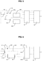
- FIG. 5 depicts one embodiment of a coherent detector, both for the transverse magnetic polarization TM and for the transverse electric polarization TE of the optical signal OS, comprising a step of wavelength recovery, replacing two tunable lasers as local oscillators.
- FIG. 5 proposes one possible diagram of a complete device that can coherently detect and process both polarization states of a complex data-carrying input optical signal, which is split into two polarization state detected and processed separately in a coherent manner.
- a data-carrying complex optical signal OS to be detected whose polarization state is assumed unknown, is injected at the input 1 of the detection system.
- a polarization splitter PBS 50 makes it possible to split both of the orthogonal components TM and TE of the complex optical signal OS and send them on two different optical paths.
- the transverse magnetic polarization component TM is transported by a polarization-maintaining fiber PMF 51 A to an optical coupler 52 A that splits the optical signal into two replicas.
- the first replica of the optical signal is routed directly to a hybrid optical circuit 53 , but the second replica is sent into a WVL-R device 54 A that erases the data and allows through a continuous signal directed towards the hybrid optical circuit 53 .
- the transverse electric polarization component TE is transported by a polarization-maintaining fiber PMF 51 B to another optical coupler 52 B that splits the optical signal into two replicas.
- the first replica of the optical signal is routed directly to a hybrid optical circuit 53 , but the second replica is sent into another WVL-R device 54 B that erases the data and allows through a continuous signal directed towards the hybrid optical circuit 53 .
- the hybrid optical circuit 53 has four input ports and four output ports which are configured to process each of the orthogonal polarization states as previously described.
- the BD-ADC device 55 completes the detection of the complex signal and recombines the information carried on both optical polarization states, thereby reconstructing the initial complex signal.
- FIG. 6 depicts another embodiment of a coherent detector, both for the transverse magnetic polarization TM and for the transverse electric polarization TE of the optical signal OS, comprising a step of wavelength recovery, replacing a tunable laser as a local oscillator.
- FIG. 6 gives one variant of FIG. 5 , wherein only one recovery wavelength is necessary, provided that this wavelength recovery function is in this case sensitive to the polarization state of the input optical signal.
- This diagram may preferentially be made of free-space optics using polarization-insensitive solid components.
- the data-carrying optical signal OS is divided into two identical replicas by an optical coupler 60 .
- the two replicas are sent respectively on two optical paths, each transported by an optical polarization-maintaining fiber PMF 61 A, 61 B.
- a polarization splitter PBS 62 makes it possible to split both of the orthogonal components TM and TE of the first replica of the complex optical signal OS and send both of them on two different optical paths.
- the transverse electric polarization component TE is transported by a polarization-maintaining fiber PMF 63 A to an input port 64 A of a hybrid optical circuit 64
- the transverse magnetic polarization component TM is transported by a polarization-maintaining fiber PMF 63 B to an input port 64 B of the hybrid optical circuit 64 .
- the second replica of the complex optical signal OS is sent into a WVL-R device 65 that erases the data and allows through a continuous signal that is split by an optical coupler 66 into two replicas respectively routed to input ports 64 C and 64 D of the hybrid optical circuit 64 .
- the hybrid optical circuit 64 has four input ports 64 A, 64 B, 64 C and 64 D and four output ports connected to a BD-ADC device 67 which completes the detection of the complex signal.
- FIG. 7 schematically depicts one embodiment of a device that enables wavelength recovery 70 comprising a tunable optical filter or a system of tunable optical filters.
- a Fabry-Perot (FP) interferometer 71 sometimes also called a Fabry-Perot filter (FFP)
- the adjustment parameter is the thickness d of the FP interferometer.
- FP Fabry-Perot
- FFP Fabry-Perot filter
- a Mach-Zehnder interferometer or a ring resonator may also be used.
- the transmission spectral response of such an FP interferometer 71 is a comb of wavelengths (or frequencies) which are spaced equally apart, and the spectral. period (or spectral distance between two teeth of the comb) is constant and called the free spectral interval (ISL) of the FP interferometer 71 .
- This ISL interval may be adjusted by the distance d separating the two mirrors 72 A and 72 B constituting the FP interferometer 71 .
- the resonance wavelengths of the FP interferometer 71 may be set by adjusting the refraction index of the material that fills in the space between the two mirrors 72 A and 72 B of the FP interferometer 71 .
- This material may, for example, be an electro-optical dielectric material (such as lithium niobate, or LiNbO 3 ), whose refraction index may be modified by varying the intensity of an electrical field that is applied to it.
- One of the resonance wavelength must then be adjusted to the information-carrying wavelength (or frequency) of the complex optical signal OS, and the interval ISL of the FP interferometer 71 must be adjusted such that none of the spectrum components of the complex optical signal OS travel through the FP interferometer 71 . For this reason, only the carrier wavelength (or frequency) of the complex optical signal OS travels through the FP interferometer 71 and is transmitted to the output port 73 of the WVL-R device 70 .
- the transmitted optical signal is continuous and single-frequency (or monochromatic), which is the goal of the functionality of the wavelength recovery device WVL-R 70 .
- This device WVL-R 70 that makes it possible to recover the wavelength may be constructed from guided waves or open-space propagation waves, the latter case being particularly well-suited to the coherent detector diagram such as the one depicted in FIG. 6 .
- the wavelength recovery device WVL-R 80 uses a ring resonator 81 that carries out the same functionality as the Fabry-Perot (FP) interferometer of FIG. 7 and has a similar transmission spectral response.
- FP Fabry-Perot
- the interval ISL is determined by the diameter of the ring of the ring resonator 81 .
- the adjustment parameter of the spectral position of the teeth of the comb is in this case the effective refraction index of the waveguide from which the ring resonator 81 is made.
- This effect of refraction index of the material that makes up the ring of the ring resonator 81 may be modified by changing the temperature using a thermal device, particularly by placing a temperature-regulating element (a resistance heating element or micro-Peltier element).
- the effect of refraction index may also be set using an electrical adjustment device, by injecting charge carriers into the material that makes up the ring by means of an electrical current.
- the ring resonator 81 is made from a semiconductor substrate (Si, InP or GaAs), and all of the described devices are made from a photonic integrated circuit (PIC).
- the waveguides are single-mode optical fibers
- the fine-tuning of the positions of the teeth of the comb may either be carried out by a change in temperature, or by a local elongation of the optical fiber under mechanical stress.
- a piezoelectric ceramic tube can be used, around which a portion of optical fiber forming the ring resonator 81 is wound.
- a ring resonator 81 Using one of the embodiments of a ring resonator 81 previously described, it is also possible obtain the wavelength recovery functionality.
- the ring resonator 81 is made from a photonic integrated circuit (PIC) and if an effort is made during design to make the ring resonator 81 polarization-insensitive, then the embodiment offered by FIG. 8 is suitable for constructing the coherent detection diagram presented in FIG. 6 .
- This design effort relates in particular to the use of light polarization-insensitive waveguides, particularly waveguides whose cross-section has axial asymmetries (such as square cross-sections), and optical couplers that are also polarization-insensitive.
- FIG. 9 depicts another embodiment of the wavelength recovery device WVL-R 90 with a tunable filter, here a Fabry-Perot (FP) interferometer 91 , followed by a feedback loop.
- a tunable filter here a Fabry-Perot (FP) interferometer 91
- FP Fabry-Perot
- An optical coupler 92 arranged at the output of the FP interferometer 91 , is used to duplicate the optical signal, in order to sample a portion of the filtered optical signal which is detected by a photodetector D 93 , while a copy of the optical signal is directed to the output 94 .
- the photodetector D 93 detects the optical signal and delivers an electrical signal which is compared to an electrical signal of a predetermined level. The result of the comparison is sent to an electromechanical device that controls one of the mirrors of the FP interferometer 91 , in order to set the distance d separating the two mirrors.
- the electrical signal is used in a feedback loop to tune the tunable filter, so that the continuous optical signal CW recovered at the output of the device enabling the recovery of the wavelength WVL-R 90 is maximized.
- This embodiment makes it possible to establish a counter-reaction on the free spectral interval ISL of the FP interferometer 91 , in order to make the FP interferometer 91 suitable for the bitrate of the complex optical signal to detect. This is because the free spectral interval ISL must not be a multiple of the bitrate in order to block the spectral components of the optical signal which must be recovered in wavelengths.
- the control system Is designed to block all spectral components of the complex optical signal, other than the carrier of the optical signal. Prior measurements of the device are needed to determine the predetermined levels to which the optical signal detected by the photodetector D 93 may be compared.
- the electronic circuit reflecting the comparison algorithm, as well as the control and mechanical actuation system for the mirrors, are not depicted in FIG. 9 .
- This embodiment may advantageously be adapted and constructed from the ring resonator of FIG. 8 .
- FIG. 10 further depicts another embodiment of the wavelength recovery device WVL-R 100 with a Fabry-Perot (FP) interferometer 101 combined with an optical amplifier such as an EDFA (Erbium Doped Fiber Amplifier) or an SOA 102 (Semiconductor Optical Amplifier) operating within its saturation regime.
- FP Fabry-Perot
- an optical amplifier such as an EDFA (Erbium Doped Fiber Amplifier) or an SOA 102 (Semiconductor Optical Amplifier) operating within its saturation regime.
- EDFA Erbium Doped Fiber Amplifier
- SOA 102 semiconductor Optical Amplifier
- a semiconductor optical amplifier SOA 102 is placed on the output path of the FP interferometer 101 .
- the SOA amplifier 102 is used in its saturation regime in order to minimize the contrast of the optical signal at the output of the FP interferometer 101 . This is because, in cases where the FP interferometer 101 is not properly adjusted or some harmonics of the modulated optical signal get through the FP interferometer 101 anyway, the output optical signal of the FP interferometer 101 is not perfectly well-known but has a low parasitic modulation.
- the SOA amplifier 102 in the saturation regime then makes it possible to minimize these parasitic modulations.
- This embodiment using an SOA amplifier may advantageously be applied in the event that a ring resonator is used in place of the FP interferometer 101 .
- a combination of a control system (see FIG. 9 ) and the use of an SOA amplifier (see FIG. 10 ) is also possible for carrying out the wavelength recovery feature.
Abstract
Description
- a source emitting an optical signal OS and optical coupler that splits the incoming optical signal OS into two replicas, the first replica of the incoming optical signal OS is sent to the first optical hybrid circuit and the second replica of the incoming optical signal OS is sent to a wavelength recovery device WVLR, whose output is a continuous-waveform optical signal CW at the central wavelength of the incoming optical signal OS, which sends it to the second optical hybrid circuit.
- such that the optical signal OS is sampled within the first hybrid circuit and the continuous waveform optical signal CW is sampled in the second hybrid circuit, and a device BDADC comprising balanced photodectors detecting optical signals at the output of the two optical hybrid circuits and an analog/digital converter ADC.
- an incoming pulsed optical signal SP is split into two propagation modes orthogonal to one another
- each propagation mode of the pulsed optical signal SP is split into two replicas, the first replica of the pulsed optical signal SP is sent to a first optical hybrid circuit and the second replica of the pulsed optical signal SP is send to a second optical hybrid circuit, an incoming optical signal OS is split into two propagation modes orthogonal to one another,
- each propagation mode of the optical signal OS is split into two replicas, the first replica of the optical signal OS is sent to the first optical hybrid circuit and the second replica of the optical signal OS is sent to a wavelength recovery device WVLR, then the continuous signal containing the recovered wavelength is sent to the second optical hybrid circuit,
- for each propagation mode, the two optical signals departing the first optical hybrid circuit and the two optical signals departing from the second optical hybrid circuit are sent to a BD-ADC device.
- an incoming optical signal OS is split into two propagation modes orthogonal to one another,
- each propagation mode of the optical signal OS is split into two replicas, the first replica of the optical signal OS is sent to an optical hybrid circuit and the second replica of the optical signal OS is sent to a wavelength recovery device WVLR, then the continuous signal containing the recovered wavelength is sent to the optical hybrid circuit,
- the four optical signals departing the optical hybrid circuit are sent to a BD-ADC device.
Claims (12)
Applications Claiming Priority (4)
| Application Number | Priority Date | Filing Date | Title |
|---|---|---|---|
| EP16305074.3A EP3200363B1 (en) | 2016-01-27 | 2016-01-27 | Linear optical sampling system and coherent detection of an optical signal |
| EP16305074 | 2016-01-27 | ||
| EP16305074.3 | 2016-01-27 | ||
| PCT/EP2017/051792 WO2017129755A1 (en) | 2016-01-27 | 2017-01-27 | System for optical linear sampling and coherent detection of an optical signal |
Publications (2)
| Publication Number | Publication Date |
|---|---|
| US20190036612A1 US20190036612A1 (en) | 2019-01-31 |
| US10594407B2 true US10594407B2 (en) | 2020-03-17 |
Family
ID=55299410
Family Applications (1)
| Application Number | Title | Priority Date | Filing Date |
|---|---|---|---|
| US16/073,106 Active US10594407B2 (en) | 2016-01-27 | 2017-01-27 | System for optical linear sampling and coherent detection of an optical signal |
Country Status (4)
| Country | Link |
|---|---|
| US (1) | US10594407B2 (en) |
| EP (1) | EP3200363B1 (en) |
| CN (1) | CN108781118B (en) |
| WO (1) | WO2017129755A1 (en) |
Families Citing this family (1)
| Publication number | Priority date | Publication date | Assignee | Title |
|---|---|---|---|---|
| CN114577337B (en) * | 2022-05-07 | 2022-07-05 | 南京航空航天大学 | Programmable wide-spectrum shaping device and spectrum measuring method and device |
Citations (6)
| Publication number | Priority date | Publication date | Assignee | Title |
|---|---|---|---|---|
| US20050185255A1 (en) | 2004-02-19 | 2005-08-25 | Doerr Christopher R. | Linear optical sampling method and apparatus |
| US20100215357A1 (en) | 2009-02-23 | 2010-08-26 | Mathias Westlund | Optical Sampling With Coherent Detection |
| US20100266291A1 (en) * | 2007-12-06 | 2010-10-21 | Pierpaolo Boffi | System and Method for Coherent Detection of Optical Signals |
| EP2709295A1 (en) | 2012-09-14 | 2014-03-19 | Alcatel Lucent | Visualisation of an optical signal by linear optical sampling |
| US20140356003A1 (en) * | 2013-05-31 | 2014-12-04 | Alcatel-Lucent | Optical receiver having a chromatic-dispersion compensation module with a multibranch filter-bank structure |
| US20160065314A1 (en) * | 2014-09-02 | 2016-03-03 | Technion Research And Development Foundation Ltd. | Self-coherent robust spectrally efficient optical transmission systems |
Family Cites Families (5)
| Publication number | Priority date | Publication date | Assignee | Title |
|---|---|---|---|---|
| WO2010095039A2 (en) * | 2009-02-23 | 2010-08-26 | Exfo Electro-Optical Engineering, Inc. | All-optical, phase sensitive optical signal sampling |
| US8805208B2 (en) * | 2012-02-03 | 2014-08-12 | Tyco Electronics Subsea Communications Llc | System and method for polarization de-multiplexing in a coherent optical receiver |
| US9369228B2 (en) * | 2012-08-14 | 2016-06-14 | Zte (Usa) Inc. | Method and apparatus for heterodyne coherent detection |
| WO2014032694A1 (en) * | 2012-08-28 | 2014-03-06 | Huawei Technologies Co., Ltd. | Optical receiver |
| US9154231B2 (en) * | 2013-01-17 | 2015-10-06 | Alcatel Lucent | Generation of an optical local-oscillator signal for a coherent-detection scheme |
-
2016
- 2016-01-27 EP EP16305074.3A patent/EP3200363B1/en active Active
-
2017
- 2017-01-27 WO PCT/EP2017/051792 patent/WO2017129755A1/en active Application Filing
- 2017-01-27 CN CN201780015497.6A patent/CN108781118B/en active Active
- 2017-01-27 US US16/073,106 patent/US10594407B2/en active Active
Patent Citations (7)
| Publication number | Priority date | Publication date | Assignee | Title |
|---|---|---|---|---|
| US20050185255A1 (en) | 2004-02-19 | 2005-08-25 | Doerr Christopher R. | Linear optical sampling method and apparatus |
| US20100266291A1 (en) * | 2007-12-06 | 2010-10-21 | Pierpaolo Boffi | System and Method for Coherent Detection of Optical Signals |
| US20100215357A1 (en) | 2009-02-23 | 2010-08-26 | Mathias Westlund | Optical Sampling With Coherent Detection |
| EP2709295A1 (en) | 2012-09-14 | 2014-03-19 | Alcatel Lucent | Visualisation of an optical signal by linear optical sampling |
| US20150249505A1 (en) | 2012-09-14 | 2015-09-03 | Alcatel Lucent | Visualization of an optical signal through linear optical sampling |
| US20140356003A1 (en) * | 2013-05-31 | 2014-12-04 | Alcatel-Lucent | Optical receiver having a chromatic-dispersion compensation module with a multibranch filter-bank structure |
| US20160065314A1 (en) * | 2014-09-02 | 2016-03-03 | Technion Research And Development Foundation Ltd. | Self-coherent robust spectrally efficient optical transmission systems |
Non-Patent Citations (1)
| Title |
|---|
| International Search Report for PCT/EP2017/051792 dated Mar. 10, 2017. |
Also Published As
| Publication number | Publication date |
|---|---|
| CN108781118B (en) | 2021-07-16 |
| EP3200363A1 (en) | 2017-08-02 |
| WO2017129755A1 (en) | 2017-08-03 |
| EP3200363B1 (en) | 2019-10-02 |
| US20190036612A1 (en) | 2019-01-31 |
| CN108781118A (en) | 2018-11-09 |
Similar Documents
| Publication | Publication Date | Title |
|---|---|---|
| JP6760976B2 (en) | Chip-based quantum key distribution | |
| US9823098B2 (en) | Apparatus for interrogating distributed optical fibre sensors using a stimulated brillouin scattering optical frequency-domain interferometer | |
| US10158481B2 (en) | Apparatus and methods for quantum key distribution | |
| Masanovic et al. | Widely tunable monolithically integrated all-optical wavelength converters in InP | |
| EP2628261B1 (en) | Broadband optical phase detection and phase noise removal with an optical resonator | |
| Fitzke et al. | Scalable network for simultaneous pairwise quantum key distribution via entanglement-based time-bin coding | |
| Grieve et al. | Characterizing nonlocal dispersion compensation in deployed telecommunications fiber | |
| Cho et al. | Stabilization of a long-armed fiber-optic single-photon interferometer | |
| Beutel et al. | Fully integrated four-channel wavelength-division multiplexed QKD receiver | |
| Lu et al. | Directly modulated vcsels with frequency comb injection for parallel communications | |
| US10594407B2 (en) | System for optical linear sampling and coherent detection of an optical signal | |
| Padmaraju et al. | Wavelength locking of a WDM silicon microring demultiplexer using dithering signals | |
| Morichetti et al. | High-sensitivity in-band OSNR monitoring system integrated on a silicon photonics chip | |
| Xiao et al. | Experimental measurement of the tolerance on optical feedback for the heterogeneous silicon quantum dot comb laser | |
| Djordjevic et al. | Entanglement Based Detection, Networking, Sensing, and Radars | |
| Lee et al. | Noise reduction in multiwavelength SOA-based ring laser by coupled dual cavities for WDM applications | |
| Gosset et al. | Phase and amplitude characterization of a 40-GHz self-pulsating DBR laser based on autocorrelation analysis | |
| Sooudi et al. | Practical and cost-effective high-fidelity optical carrier dissemination using coherent communication techniques | |
| Llorente et al. | Linear and nonlinear crosstalk evaluation in DWDM networks using optical Fourier transformers | |
| Wang et al. | High quality entanglement distribution through telecommunication fiber using near-infrared non-degenerate photon pairs | |
| Zhang | Hybrid Si/III-V Lasers for Next-generation Coherent Optical Communication | |
| Geng | Comb based Optical Signal Processing | |
| Grein et al. | Sub-wavelength stabilization of long, deployed optical fibers for quantum networks | |
| Power | All-optical signal processing using semiconductor optical amplifiers for next generation optical networks | |
| Power | All-optical signal processing using semiconductor optical amplifiers for |
Legal Events
| Date | Code | Title | Description |
|---|---|---|---|
| FEPP | Fee payment procedure |
Free format text: ENTITY STATUS SET TO UNDISCOUNTED (ORIGINAL EVENT CODE: BIG.); ENTITY STATUS OF PATENT OWNER: LARGE ENTITY |
|
| AS | Assignment |
Owner name: ALCATEL LUCENT, FRANCE Free format text: ASSIGNMENT OF ASSIGNORS INTEREST;ASSIGNORS:SHEN, ALEXANDRE;PROVOST, JEAN-GUY;REEL/FRAME:047820/0331 Effective date: 20181115 |
|
| STPP | Information on status: patent application and granting procedure in general |
Free format text: DOCKETED NEW CASE - READY FOR EXAMINATION |
|
| STPP | Information on status: patent application and granting procedure in general |
Free format text: NON FINAL ACTION MAILED |
|
| STPP | Information on status: patent application and granting procedure in general |
Free format text: FINAL REJECTION MAILED |
|
| STPP | Information on status: patent application and granting procedure in general |
Free format text: NOTICE OF ALLOWANCE MAILED -- APPLICATION RECEIVED IN OFFICE OF PUBLICATIONS |
|
| STPP | Information on status: patent application and granting procedure in general |
Free format text: PUBLICATIONS -- ISSUE FEE PAYMENT VERIFIED |
|
| STCF | Information on status: patent grant |
Free format text: PATENTED CASE |
|
| MAFP | Maintenance fee payment |
Free format text: PAYMENT OF MAINTENANCE FEE, 4TH YEAR, LARGE ENTITY (ORIGINAL EVENT CODE: M1551); ENTITY STATUS OF PATENT OWNER: LARGE ENTITY Year of fee payment: 4 |