US10573528B2 - Two-color self-aligned double patterning (SADP) to yield static random access memory (SRAM) and dense logic - Google Patents
Two-color self-aligned double patterning (SADP) to yield static random access memory (SRAM) and dense logic Download PDFInfo
- Publication number
- US10573528B2 US10573528B2 US15/842,841 US201715842841A US10573528B2 US 10573528 B2 US10573528 B2 US 10573528B2 US 201715842841 A US201715842841 A US 201715842841A US 10573528 B2 US10573528 B2 US 10573528B2
- Authority
- US
- United States
- Prior art keywords
- semiconductor structure
- fin
- surface features
- fins
- etching
- Prior art date
- Legal status (The legal status is an assumption and is not a legal conclusion. Google has not performed a legal analysis and makes no representation as to the accuracy of the status listed.)
- Active
Links
- 238000000059 patterning Methods 0.000 title description 7
- 230000003068 static effect Effects 0.000 title description 6
- 239000004065 semiconductor Substances 0.000 claims abstract description 108
- 238000005530 etching Methods 0.000 claims abstract description 53
- 125000006850 spacer group Chemical group 0.000 claims abstract description 36
- 238000001459 lithography Methods 0.000 claims abstract description 33
- 230000015572 biosynthetic process Effects 0.000 claims abstract description 31
- 239000000463 material Substances 0.000 claims abstract description 29
- 238000000034 method Methods 0.000 claims description 69
- 239000011295 pitch Substances 0.000 claims description 69
- 238000000151 deposition Methods 0.000 claims description 17
- 229910021417 amorphous silicon Inorganic materials 0.000 claims description 13
- 238000001020 plasma etching Methods 0.000 claims description 13
- 229910003481 amorphous carbon Inorganic materials 0.000 claims description 12
- 230000008021 deposition Effects 0.000 claims description 10
- 239000000758 substrate Substances 0.000 claims description 9
- 229920002120 photoresistant polymer Polymers 0.000 claims description 7
- 238000005520 cutting process Methods 0.000 claims description 6
- 239000010410 layer Substances 0.000 description 39
- 238000004519 manufacturing process Methods 0.000 description 20
- 230000008569 process Effects 0.000 description 14
- VYPSYNLAJGMNEJ-UHFFFAOYSA-N Silicium dioxide Chemical compound O=[Si]=O VYPSYNLAJGMNEJ-UHFFFAOYSA-N 0.000 description 13
- HLLICFJUWSZHRJ-UHFFFAOYSA-N tioxidazole Chemical compound CCCOC1=CC=C2N=C(NC(=O)OC)SC2=C1 HLLICFJUWSZHRJ-UHFFFAOYSA-N 0.000 description 10
- 238000013461 design Methods 0.000 description 9
- 238000013459 approach Methods 0.000 description 8
- 230000000670 limiting effect Effects 0.000 description 8
- 238000012545 processing Methods 0.000 description 7
- 229910052814 silicon oxide Inorganic materials 0.000 description 5
- XUIMIQQOPSSXEZ-UHFFFAOYSA-N Silicon Chemical compound [Si] XUIMIQQOPSSXEZ-UHFFFAOYSA-N 0.000 description 4
- 238000010420 art technique Methods 0.000 description 4
- 239000011248 coating agent Substances 0.000 description 4
- 238000000576 coating method Methods 0.000 description 4
- 238000012986 modification Methods 0.000 description 4
- 230000004048 modification Effects 0.000 description 4
- 229910052710 silicon Inorganic materials 0.000 description 4
- 239000010703 silicon Substances 0.000 description 4
- 239000000377 silicon dioxide Substances 0.000 description 4
- 231100000331 toxic Toxicity 0.000 description 4
- 230000002588 toxic effect Effects 0.000 description 4
- 238000012546 transfer Methods 0.000 description 4
- 235000012431 wafers Nutrition 0.000 description 4
- 229910003087 TiOx Inorganic materials 0.000 description 3
- 230000008901 benefit Effects 0.000 description 3
- 230000000694 effects Effects 0.000 description 3
- 230000005669 field effect Effects 0.000 description 3
- 229910044991 metal oxide Inorganic materials 0.000 description 3
- 150000004706 metal oxides Chemical class 0.000 description 3
- 239000000126 substance Substances 0.000 description 3
- 229910052581 Si3N4 Inorganic materials 0.000 description 2
- GWEVSGVZZGPLCZ-UHFFFAOYSA-N Titan oxide Chemical compound O=[Ti]=O GWEVSGVZZGPLCZ-UHFFFAOYSA-N 0.000 description 2
- 230000009286 beneficial effect Effects 0.000 description 2
- 229910052681 coesite Inorganic materials 0.000 description 2
- 229910052906 cristobalite Inorganic materials 0.000 description 2
- 230000009977 dual effect Effects 0.000 description 2
- 238000005516 engineering process Methods 0.000 description 2
- 239000012467 final product Substances 0.000 description 2
- 230000000873 masking effect Effects 0.000 description 2
- 230000036961 partial effect Effects 0.000 description 2
- 230000009467 reduction Effects 0.000 description 2
- 235000012239 silicon dioxide Nutrition 0.000 description 2
- HQVNEWCFYHHQES-UHFFFAOYSA-N silicon nitride Chemical compound N12[Si]34N5[Si]62N3[Si]51N64 HQVNEWCFYHHQES-UHFFFAOYSA-N 0.000 description 2
- 229910052682 stishovite Inorganic materials 0.000 description 2
- OGIDPMRJRNCKJF-UHFFFAOYSA-N titanium oxide Inorganic materials [Ti]=O OGIDPMRJRNCKJF-UHFFFAOYSA-N 0.000 description 2
- 229910052905 tridymite Inorganic materials 0.000 description 2
- 229910020286 SiOxNy Inorganic materials 0.000 description 1
- 230000006978 adaptation Effects 0.000 description 1
- 230000003466 anti-cipated effect Effects 0.000 description 1
- 239000006117 anti-reflective coating Substances 0.000 description 1
- 230000004888 barrier function Effects 0.000 description 1
- 229910052799 carbon Inorganic materials 0.000 description 1
- 229910010293 ceramic material Inorganic materials 0.000 description 1
- 238000012512 characterization method Methods 0.000 description 1
- 239000007795 chemical reaction product Substances 0.000 description 1
- 239000003086 colorant Substances 0.000 description 1
- 238000004040 coloring Methods 0.000 description 1
- 230000000295 complement effect Effects 0.000 description 1
- 239000002131 composite material Substances 0.000 description 1
- 150000001875 compounds Chemical class 0.000 description 1
- 230000001010 compromised effect Effects 0.000 description 1
- 230000007423 decrease Effects 0.000 description 1
- 238000001312 dry etching Methods 0.000 description 1
- 230000008030 elimination Effects 0.000 description 1
- 238000003379 elimination reaction Methods 0.000 description 1
- 230000006870 function Effects 0.000 description 1
- 238000005286 illumination Methods 0.000 description 1
- 239000012212 insulator Substances 0.000 description 1
- 239000013067 intermediate product Substances 0.000 description 1
- 238000005457 optimization Methods 0.000 description 1
- 238000000206 photolithography Methods 0.000 description 1
- 230000002441 reversible effect Effects 0.000 description 1
- 238000006467 substitution reaction Methods 0.000 description 1
- 239000010936 titanium Substances 0.000 description 1
- 238000001039 wet etching Methods 0.000 description 1
Images


Classifications
-
- H—ELECTRICITY
- H01—ELECTRIC ELEMENTS
- H01L—SEMICONDUCTOR DEVICES NOT COVERED BY CLASS H10
- H01L29/00—Semiconductor devices specially adapted for rectifying, amplifying, oscillating or switching and having potential barriers; Capacitors or resistors having potential barriers, e.g. a PN-junction depletion layer or carrier concentration layer; Details of semiconductor bodies or of electrodes thereof ; Multistep manufacturing processes therefor
- H01L29/66—Types of semiconductor device ; Multistep manufacturing processes therefor
- H01L29/66007—Multistep manufacturing processes
- H01L29/66075—Multistep manufacturing processes of devices having semiconductor bodies comprising group 14 or group 13/15 materials
- H01L29/66227—Multistep manufacturing processes of devices having semiconductor bodies comprising group 14 or group 13/15 materials the devices being controllable only by the electric current supplied or the electric potential applied, to an electrode which does not carry the current to be rectified, amplified or switched, e.g. three-terminal devices
- H01L29/66409—Unipolar field-effect transistors
- H01L29/66477—Unipolar field-effect transistors with an insulated gate, i.e. MISFET
- H01L29/66787—Unipolar field-effect transistors with an insulated gate, i.e. MISFET with a gate at the side of the channel
- H01L29/66795—Unipolar field-effect transistors with an insulated gate, i.e. MISFET with a gate at the side of the channel with a horizontal current flow in a vertical sidewall of a semiconductor body, e.g. FinFET, MuGFET
- H01L29/6681—Unipolar field-effect transistors with an insulated gate, i.e. MISFET with a gate at the side of the channel with a horizontal current flow in a vertical sidewall of a semiconductor body, e.g. FinFET, MuGFET using dummy structures having essentially the same shape as the semiconductor body, e.g. to provide stability
-
- H—ELECTRICITY
- H01—ELECTRIC ELEMENTS
- H01L—SEMICONDUCTOR DEVICES NOT COVERED BY CLASS H10
- H01L21/00—Processes or apparatus adapted for the manufacture or treatment of semiconductor or solid state devices or of parts thereof
- H01L21/02—Manufacture or treatment of semiconductor devices or of parts thereof
- H01L21/027—Making masks on semiconductor bodies for further photolithographic processing not provided for in group H01L21/18 or H01L21/34
- H01L21/033—Making masks on semiconductor bodies for further photolithographic processing not provided for in group H01L21/18 or H01L21/34 comprising inorganic layers
- H01L21/0332—Making masks on semiconductor bodies for further photolithographic processing not provided for in group H01L21/18 or H01L21/34 comprising inorganic layers characterised by their composition, e.g. multilayer masks, materials
-
- H—ELECTRICITY
- H01—ELECTRIC ELEMENTS
- H01L—SEMICONDUCTOR DEVICES NOT COVERED BY CLASS H10
- H01L21/00—Processes or apparatus adapted for the manufacture or treatment of semiconductor or solid state devices or of parts thereof
- H01L21/02—Manufacture or treatment of semiconductor devices or of parts thereof
- H01L21/027—Making masks on semiconductor bodies for further photolithographic processing not provided for in group H01L21/18 or H01L21/34
- H01L21/033—Making masks on semiconductor bodies for further photolithographic processing not provided for in group H01L21/18 or H01L21/34 comprising inorganic layers
- H01L21/0334—Making masks on semiconductor bodies for further photolithographic processing not provided for in group H01L21/18 or H01L21/34 comprising inorganic layers characterised by their size, orientation, disposition, behaviour, shape, in horizontal or vertical plane
- H01L21/0335—Making masks on semiconductor bodies for further photolithographic processing not provided for in group H01L21/18 or H01L21/34 comprising inorganic layers characterised by their size, orientation, disposition, behaviour, shape, in horizontal or vertical plane characterised by their behaviour during the process, e.g. soluble masks, redeposited masks
-
- H—ELECTRICITY
- H01—ELECTRIC ELEMENTS
- H01L—SEMICONDUCTOR DEVICES NOT COVERED BY CLASS H10
- H01L21/00—Processes or apparatus adapted for the manufacture or treatment of semiconductor or solid state devices or of parts thereof
- H01L21/02—Manufacture or treatment of semiconductor devices or of parts thereof
- H01L21/027—Making masks on semiconductor bodies for further photolithographic processing not provided for in group H01L21/18 or H01L21/34
- H01L21/033—Making masks on semiconductor bodies for further photolithographic processing not provided for in group H01L21/18 or H01L21/34 comprising inorganic layers
- H01L21/0334—Making masks on semiconductor bodies for further photolithographic processing not provided for in group H01L21/18 or H01L21/34 comprising inorganic layers characterised by their size, orientation, disposition, behaviour, shape, in horizontal or vertical plane
- H01L21/0337—Making masks on semiconductor bodies for further photolithographic processing not provided for in group H01L21/18 or H01L21/34 comprising inorganic layers characterised by their size, orientation, disposition, behaviour, shape, in horizontal or vertical plane characterised by the process involved to create the mask, e.g. lift-off masks, sidewalls, or to modify the mask, e.g. pre-treatment, post-treatment
-
- H—ELECTRICITY
- H01—ELECTRIC ELEMENTS
- H01L—SEMICONDUCTOR DEVICES NOT COVERED BY CLASS H10
- H01L21/00—Processes or apparatus adapted for the manufacture or treatment of semiconductor or solid state devices or of parts thereof
- H01L21/02—Manufacture or treatment of semiconductor devices or of parts thereof
- H01L21/04—Manufacture or treatment of semiconductor devices or of parts thereof the devices having potential barriers, e.g. a PN junction, depletion layer or carrier concentration layer
- H01L21/18—Manufacture or treatment of semiconductor devices or of parts thereof the devices having potential barriers, e.g. a PN junction, depletion layer or carrier concentration layer the devices having semiconductor bodies comprising elements of Group IV of the Periodic Table or AIIIBV compounds with or without impurities, e.g. doping materials
- H01L21/30—Treatment of semiconductor bodies using processes or apparatus not provided for in groups H01L21/20 - H01L21/26
- H01L21/302—Treatment of semiconductor bodies using processes or apparatus not provided for in groups H01L21/20 - H01L21/26 to change their surface-physical characteristics or shape, e.g. etching, polishing, cutting
- H01L21/306—Chemical or electrical treatment, e.g. electrolytic etching
- H01L21/3065—Plasma etching; Reactive-ion etching
-
- H—ELECTRICITY
- H01—ELECTRIC ELEMENTS
- H01L—SEMICONDUCTOR DEVICES NOT COVERED BY CLASS H10
- H01L21/00—Processes or apparatus adapted for the manufacture or treatment of semiconductor or solid state devices or of parts thereof
- H01L21/02—Manufacture or treatment of semiconductor devices or of parts thereof
- H01L21/04—Manufacture or treatment of semiconductor devices or of parts thereof the devices having potential barriers, e.g. a PN junction, depletion layer or carrier concentration layer
- H01L21/18—Manufacture or treatment of semiconductor devices or of parts thereof the devices having potential barriers, e.g. a PN junction, depletion layer or carrier concentration layer the devices having semiconductor bodies comprising elements of Group IV of the Periodic Table or AIIIBV compounds with or without impurities, e.g. doping materials
- H01L21/30—Treatment of semiconductor bodies using processes or apparatus not provided for in groups H01L21/20 - H01L21/26
- H01L21/302—Treatment of semiconductor bodies using processes or apparatus not provided for in groups H01L21/20 - H01L21/26 to change their surface-physical characteristics or shape, e.g. etching, polishing, cutting
- H01L21/306—Chemical or electrical treatment, e.g. electrolytic etching
- H01L21/308—Chemical or electrical treatment, e.g. electrolytic etching using masks
- H01L21/3081—Chemical or electrical treatment, e.g. electrolytic etching using masks characterised by their composition, e.g. multilayer masks, materials
-
- H—ELECTRICITY
- H01—ELECTRIC ELEMENTS
- H01L—SEMICONDUCTOR DEVICES NOT COVERED BY CLASS H10
- H01L21/00—Processes or apparatus adapted for the manufacture or treatment of semiconductor or solid state devices or of parts thereof
- H01L21/02—Manufacture or treatment of semiconductor devices or of parts thereof
- H01L21/04—Manufacture or treatment of semiconductor devices or of parts thereof the devices having potential barriers, e.g. a PN junction, depletion layer or carrier concentration layer
- H01L21/18—Manufacture or treatment of semiconductor devices or of parts thereof the devices having potential barriers, e.g. a PN junction, depletion layer or carrier concentration layer the devices having semiconductor bodies comprising elements of Group IV of the Periodic Table or AIIIBV compounds with or without impurities, e.g. doping materials
- H01L21/30—Treatment of semiconductor bodies using processes or apparatus not provided for in groups H01L21/20 - H01L21/26
- H01L21/302—Treatment of semiconductor bodies using processes or apparatus not provided for in groups H01L21/20 - H01L21/26 to change their surface-physical characteristics or shape, e.g. etching, polishing, cutting
- H01L21/306—Chemical or electrical treatment, e.g. electrolytic etching
- H01L21/308—Chemical or electrical treatment, e.g. electrolytic etching using masks
- H01L21/3083—Chemical or electrical treatment, e.g. electrolytic etching using masks characterised by their size, orientation, disposition, behaviour, shape, in horizontal or vertical plane
- H01L21/3085—Chemical or electrical treatment, e.g. electrolytic etching using masks characterised by their size, orientation, disposition, behaviour, shape, in horizontal or vertical plane characterised by their behaviour during the process, e.g. soluble masks, redeposited masks
-
- H—ELECTRICITY
- H01—ELECTRIC ELEMENTS
- H01L—SEMICONDUCTOR DEVICES NOT COVERED BY CLASS H10
- H01L21/00—Processes or apparatus adapted for the manufacture or treatment of semiconductor or solid state devices or of parts thereof
- H01L21/02—Manufacture or treatment of semiconductor devices or of parts thereof
- H01L21/04—Manufacture or treatment of semiconductor devices or of parts thereof the devices having potential barriers, e.g. a PN junction, depletion layer or carrier concentration layer
- H01L21/18—Manufacture or treatment of semiconductor devices or of parts thereof the devices having potential barriers, e.g. a PN junction, depletion layer or carrier concentration layer the devices having semiconductor bodies comprising elements of Group IV of the Periodic Table or AIIIBV compounds with or without impurities, e.g. doping materials
- H01L21/30—Treatment of semiconductor bodies using processes or apparatus not provided for in groups H01L21/20 - H01L21/26
- H01L21/302—Treatment of semiconductor bodies using processes or apparatus not provided for in groups H01L21/20 - H01L21/26 to change their surface-physical characteristics or shape, e.g. etching, polishing, cutting
- H01L21/306—Chemical or electrical treatment, e.g. electrolytic etching
- H01L21/308—Chemical or electrical treatment, e.g. electrolytic etching using masks
- H01L21/3083—Chemical or electrical treatment, e.g. electrolytic etching using masks characterised by their size, orientation, disposition, behaviour, shape, in horizontal or vertical plane
- H01L21/3086—Chemical or electrical treatment, e.g. electrolytic etching using masks characterised by their size, orientation, disposition, behaviour, shape, in horizontal or vertical plane characterised by the process involved to create the mask, e.g. lift-off masks, sidewalls, or to modify the mask, e.g. pre-treatment, post-treatment
-
- H—ELECTRICITY
- H01—ELECTRIC ELEMENTS
- H01L—SEMICONDUCTOR DEVICES NOT COVERED BY CLASS H10
- H01L21/00—Processes or apparatus adapted for the manufacture or treatment of semiconductor or solid state devices or of parts thereof
- H01L21/02—Manufacture or treatment of semiconductor devices or of parts thereof
- H01L21/04—Manufacture or treatment of semiconductor devices or of parts thereof the devices having potential barriers, e.g. a PN junction, depletion layer or carrier concentration layer
- H01L21/18—Manufacture or treatment of semiconductor devices or of parts thereof the devices having potential barriers, e.g. a PN junction, depletion layer or carrier concentration layer the devices having semiconductor bodies comprising elements of Group IV of the Periodic Table or AIIIBV compounds with or without impurities, e.g. doping materials
- H01L21/30—Treatment of semiconductor bodies using processes or apparatus not provided for in groups H01L21/20 - H01L21/26
- H01L21/31—Treatment of semiconductor bodies using processes or apparatus not provided for in groups H01L21/20 - H01L21/26 to form insulating layers thereon, e.g. for masking or by using photolithographic techniques; After treatment of these layers; Selection of materials for these layers
- H01L21/3105—After-treatment
- H01L21/311—Etching the insulating layers by chemical or physical means
- H01L21/31105—Etching inorganic layers
- H01L21/31111—Etching inorganic layers by chemical means
- H01L21/31116—Etching inorganic layers by chemical means by dry-etching
-
- H—ELECTRICITY
- H01—ELECTRIC ELEMENTS
- H01L—SEMICONDUCTOR DEVICES NOT COVERED BY CLASS H10
- H01L21/00—Processes or apparatus adapted for the manufacture or treatment of semiconductor or solid state devices or of parts thereof
- H01L21/70—Manufacture or treatment of devices consisting of a plurality of solid state components formed in or on a common substrate or of parts thereof; Manufacture of integrated circuit devices or of parts thereof
- H01L21/77—Manufacture or treatment of devices consisting of a plurality of solid state components or integrated circuits formed in, or on, a common substrate
- H01L21/78—Manufacture or treatment of devices consisting of a plurality of solid state components or integrated circuits formed in, or on, a common substrate with subsequent division of the substrate into plural individual devices
- H01L21/82—Manufacture or treatment of devices consisting of a plurality of solid state components or integrated circuits formed in, or on, a common substrate with subsequent division of the substrate into plural individual devices to produce devices, e.g. integrated circuits, each consisting of a plurality of components
- H01L21/822—Manufacture or treatment of devices consisting of a plurality of solid state components or integrated circuits formed in, or on, a common substrate with subsequent division of the substrate into plural individual devices to produce devices, e.g. integrated circuits, each consisting of a plurality of components the substrate being a semiconductor, using silicon technology
- H01L21/8232—Field-effect technology
- H01L21/8234—MIS technology, i.e. integration processes of field effect transistors of the conductor-insulator-semiconductor type
- H01L21/823431—MIS technology, i.e. integration processes of field effect transistors of the conductor-insulator-semiconductor type with a particular manufacturing method of transistors with a horizontal current flow in a vertical sidewall of a semiconductor body, e.g. FinFET, MuGFET
-
- H—ELECTRICITY
- H01—ELECTRIC ELEMENTS
- H01L—SEMICONDUCTOR DEVICES NOT COVERED BY CLASS H10
- H01L27/00—Devices consisting of a plurality of semiconductor or other solid-state components formed in or on a common substrate
- H01L27/02—Devices consisting of a plurality of semiconductor or other solid-state components formed in or on a common substrate including semiconductor components specially adapted for rectifying, oscillating, amplifying or switching and having potential barriers; including integrated passive circuit elements having potential barriers
- H01L27/04—Devices consisting of a plurality of semiconductor or other solid-state components formed in or on a common substrate including semiconductor components specially adapted for rectifying, oscillating, amplifying or switching and having potential barriers; including integrated passive circuit elements having potential barriers the substrate being a semiconductor body
- H01L27/08—Devices consisting of a plurality of semiconductor or other solid-state components formed in or on a common substrate including semiconductor components specially adapted for rectifying, oscillating, amplifying or switching and having potential barriers; including integrated passive circuit elements having potential barriers the substrate being a semiconductor body including only semiconductor components of a single kind
- H01L27/085—Devices consisting of a plurality of semiconductor or other solid-state components formed in or on a common substrate including semiconductor components specially adapted for rectifying, oscillating, amplifying or switching and having potential barriers; including integrated passive circuit elements having potential barriers the substrate being a semiconductor body including only semiconductor components of a single kind including field-effect components only
- H01L27/088—Devices consisting of a plurality of semiconductor or other solid-state components formed in or on a common substrate including semiconductor components specially adapted for rectifying, oscillating, amplifying or switching and having potential barriers; including integrated passive circuit elements having potential barriers the substrate being a semiconductor body including only semiconductor components of a single kind including field-effect components only the components being field-effect transistors with insulated gate
- H01L27/0886—Devices consisting of a plurality of semiconductor or other solid-state components formed in or on a common substrate including semiconductor components specially adapted for rectifying, oscillating, amplifying or switching and having potential barriers; including integrated passive circuit elements having potential barriers the substrate being a semiconductor body including only semiconductor components of a single kind including field-effect components only the components being field-effect transistors with insulated gate including transistors with a horizontal current flow in a vertical sidewall of a semiconductor body, e.g. FinFET, MuGFET
-
- H—ELECTRICITY
- H01—ELECTRIC ELEMENTS
- H01L—SEMICONDUCTOR DEVICES NOT COVERED BY CLASS H10
- H01L29/00—Semiconductor devices specially adapted for rectifying, amplifying, oscillating or switching and having potential barriers; Capacitors or resistors having potential barriers, e.g. a PN-junction depletion layer or carrier concentration layer; Details of semiconductor bodies or of electrodes thereof ; Multistep manufacturing processes therefor
- H01L29/66—Types of semiconductor device ; Multistep manufacturing processes therefor
- H01L29/66007—Multistep manufacturing processes
- H01L29/66075—Multistep manufacturing processes of devices having semiconductor bodies comprising group 14 or group 13/15 materials
- H01L29/66227—Multistep manufacturing processes of devices having semiconductor bodies comprising group 14 or group 13/15 materials the devices being controllable only by the electric current supplied or the electric potential applied, to an electrode which does not carry the current to be rectified, amplified or switched, e.g. three-terminal devices
- H01L29/66409—Unipolar field-effect transistors
- H01L29/66477—Unipolar field-effect transistors with an insulated gate, i.e. MISFET
- H01L29/66787—Unipolar field-effect transistors with an insulated gate, i.e. MISFET with a gate at the side of the channel
- H01L29/66795—Unipolar field-effect transistors with an insulated gate, i.e. MISFET with a gate at the side of the channel with a horizontal current flow in a vertical sidewall of a semiconductor body, e.g. FinFET, MuGFET
-
- H—ELECTRICITY
- H10—SEMICONDUCTOR DEVICES; ELECTRIC SOLID-STATE DEVICES NOT OTHERWISE PROVIDED FOR
- H10B—ELECTRONIC MEMORY DEVICES
- H10B10/00—Static random access memory [SRAM] devices
- H10B10/12—Static random access memory [SRAM] devices comprising a MOSFET load element
-
- H01L27/1104—
-
- H01L27/1116—
-
- H—ELECTRICITY
- H01—ELECTRIC ELEMENTS
- H01L—SEMICONDUCTOR DEVICES NOT COVERED BY CLASS H10
- H01L29/00—Semiconductor devices specially adapted for rectifying, amplifying, oscillating or switching and having potential barriers; Capacitors or resistors having potential barriers, e.g. a PN-junction depletion layer or carrier concentration layer; Details of semiconductor bodies or of electrodes thereof ; Multistep manufacturing processes therefor
- H01L29/66—Types of semiconductor device ; Multistep manufacturing processes therefor
- H01L29/68—Types of semiconductor device ; Multistep manufacturing processes therefor controllable by only the electric current supplied, or only the electric potential applied, to an electrode which does not carry the current to be rectified, amplified or switched
- H01L29/76—Unipolar devices, e.g. field effect transistors
- H01L29/772—Field effect transistors
- H01L29/78—Field effect transistors with field effect produced by an insulated gate
- H01L29/785—Field effect transistors with field effect produced by an insulated gate having a channel with a horizontal current flow in a vertical sidewall of a semiconductor body, e.g. FinFET, MuGFET
-
- H—ELECTRICITY
- H10—SEMICONDUCTOR DEVICES; ELECTRIC SOLID-STATE DEVICES NOT OTHERWISE PROVIDED FOR
- H10B—ELECTRONIC MEMORY DEVICES
- H10B10/00—Static random access memory [SRAM] devices
- H10B10/18—Peripheral circuit regions
Definitions
- the present invention relates to the electrical and electronic arts, and more specifically, to semiconductor fabrication techniques and the like.
- MOSFETs metal oxide semiconductor field effect transistors
- CMOS complementary metal oxide semiconductor
- Semiconductor fins are typically formed utilizing a sidewall image transfer (SIT) process, since the same provides sub-lithographic line widths.
- SIT sidewall image transfer
- spacers are formed on each sidewall surface of a sacrificial mandrel that is formed on a topmost semiconductor material of a substrate. The sacrificial mandrel is removed and the remaining spacers are used as an etch mask to etch the topmost semiconductor material of the substrate. The spacers are then removed after each semiconductor fin has been formed.
- another exemplary method includes providing a semiconductor structure having a generally planar surface; carrying out first lithography and etching on the semiconductor structure with a first mask, to provide a first intermediate semiconductor structure having a first set of surface features corresponding to a first portion of desired fin formation mandrels; and carrying out second lithography and etching on the first intermediate semiconductor structure, using a second mask, to provide a second intermediate semiconductor structure having a second set of surface features corresponding to a second portion of the desired fin formation mandrels.
- the first set of surface features have a first pitch and the second set of surface features have a second pitch different than the first pitch.
- one or more embodiments reduce, or completely eliminate, undesirable formation of dummy fins, with manufacturing processes that can feasibly be implemented, and with finer fin pitch than can be achieved by conventional lithography.
- FIG. 1 is a plan view of an intermediate stage in semiconductor structure fabrication in accordance with the prior art, showing undesirable dummy fins;
- FIG. 3 is a plan view of another intermediate stage in semiconductor structure fabrication in accordance with the prior art, showing undesirable dummy fins;
- FIG. 4 is a plan view of an intermediate stage in semiconductor structure fabrication in accordance with an aspect of the invention, showing that undesirable dummy fins are not formed;
- FIG. 5 is a plan view of an intermediate stage in semiconductor structure fabrication in accordance with an aspect of the invention, with variable mandrel spacing;
- FIGS. 8 and 9 show a side cross-sectional view of a second color structure in accordance with an aspect of the invention post lithography and post etch respectively;
- FIG. 10 shows etching of the structure of FIG. 9 to create features in a titanium oxide layer, in accordance with an aspect of the invention
- FIG. 12 shows top spacer deposition over the structure of FIG. 11 , in accordance with an aspect of the invention
- FIG. 13 shows the structure of FIG. 12 after top spacer etch-back, in accordance with an aspect of the invention
- FIG. 14 shows the structure of FIG. 13 after mandrel pull (enlarged view), in accordance with an aspect of the invention
- FIG. 15 shows the structure of FIG. 14 after BM (bottom mandrel) reactive ion etching (RIE) (enlarged view), in accordance with an aspect of the invention
- FIG. 16 shows a plan view of a sidewall merge approach in accordance with the prior art.
- FIGS. 17 and 18 show exemplary dimensions), in accordance with aspects of the invention.
- FIGS. 6-15 schematically illustrate several exemplary sequences of fabrication steps that may be employed in obtaining static random access memory (SRAM) and/or dense logic.
- SRAM static random access memory
- FIGS. 6-15 schematically illustrate several exemplary sequences of fabrication steps that may be employed in obtaining static random access memory (SRAM) and/or dense logic.
- SRAM static random access memory
- FIGS. 6-15 schematically illustrate several exemplary sequences of fabrication steps that may be employed in obtaining static random access memory (SRAM) and/or dense logic.
- SRAM static random access memory
- FIGS. 6-15 schematically illustrate several exemplary sequences of fabrication steps that may be employed in obtaining static random access memory (SRAM) and/or dense logic.
- SIT2 sidewall image transfer twice
- SAQP self-aligned quadruple patterning
- One or more embodiments advantageously employ SIT1 (sidewall image transfer once)/SADP (Self-Aligned Double Patterning) for SRAM and dense logic.
- SIT1 sidewall image transfer once
- SADP Self-Aligned Double Patterning
- two-color mandrel There may be some possible penalty on the uniformity of the active FINA of the device because of the two color overlay in the same layout area.
- the device source-drain (S/D) capacitance may be slightly worse, or better, than prior techniques. This is because Fin pitch uniformity is an important factor for device performance. With 2 color SADP, meaning two mandrel lithography steps, the overlay could cause “pitch walking” (wherein the Fin-to-Fin distances are not equal) in the Fin structure.
- the pitches are not exactly the same in the final product.
- such overlay effect can be minimized in real production.
- one or more embodiments are particularly pertinent to “BIG” devices; e.g., more than two active fins and typically four or more active fins.
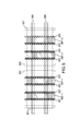
- FIG. 1 which is a top view of a prior art approach, note extreme variable fin pitch “squeeze” below 30 nm from SIT2 (SAQP), resulting in unavoidable dummy FINI that cannot be readily cleaned up.
- FIG. 2 shows a corresponding desired design. Note the undesirable inactive FINI 101 , 103 , 105 , 107 , 109 , 111 , 113 , and 115 in FIG. 1 which are not present in the desired design shown in FIG. 2 .
- the desirable, active fins are numbered 121 , 123 , 125 , 127 , 129 , 131 , 133 , and 135 .
- transverse structures 199 , 299 represent gate or contact structures as will be apparent to the skilled artisan; to avoid clutter not all the transverse structures are numbered.
- the centerline spacing of the dummy fin 111 and active fin 127 can be 26 nm; the centerline spacing of the dummy fins 103 - 105 can be 24 nm; and the centerline spacing of the dummy fin 113 and active fin 129 can be 26 nm.
- the desired design of FIG. 2 can be achieved using relaxed fin patterning in SIT1 (SADP) to make SRAM, without undesirable dummy FINI next to desired active FINA, and without the need for RX masking.
- the regions 189 , 187 , 185 , 183 represent sacrificial mandrel locations—reference is made to the aforementioned Colburn patent.
- FIG. 3 shows a prior art approach using SIT2 (SAQP) with a uniform fin pitch of 30 nm (e.g., 8 nm wide fins with 22 nm between the walls of the fins).
- SAQP SIT2
- the example of FIG. 3 is for a standard logic topology of four-fin devices; e.g., a dual inverter or an XOR gate. Extreme precision is necessary to remove the undesirable dummy fins.
- FIG. 4 shows a dual mandrel pattern for “BIG” devices in accordance with an aspect of the invention, wherein fabrication using a single pattern is not feasible.
- a mandrel pitch of 60 nm is employed with two colors.
- dummy fins do not form.
- a “pseudo-uniform” fin pitch of 30 is achieved.
- an overlay (OL) of 6 nm can be used to “squeeze” a fin pitch of 30 nm down to a fin pitch of 24 nm.
- active fins 421 , 423 , 425 , 427 , 429 , 431 , 433 , 435 are shown for reference; i.e., to show where dummy fins would have formed in the prior art process, but are not formed in this aspect.
- transverse structures 499 which represent gate or contact structures as will be apparent to the skilled artisan.
- the space between fins 421 - 423 , 423 - 425 , 425 - 427 and between fins 429 - 431 , 431 - 433 , and 433 - 435 can be, for example, 22 nm.
- the space between fins 427 - 429 can be, for example, 82 nm.
- the centerline distance between fins 427 - 429 can thus be 90 nm, while the centerline distance between fins 421 - 425 and 429 - 433 can thus be 60 nm.
- transverse structures 699 which represent gate or contact structures as will be apparent to the skilled artisan.
- the space between fins 621 - 623 , 625 - 627 and between fins 629 - 631 , and 633 - 635 can be, for example, 22 nm.
- the space between fins 627 - 629 can be, for example, 76 nm.
- the space between fins 623 - 625 and between fins 631 - 633 can be, for example, 28 nm.
- the centerline distance between fins 627 - 629 can thus be 84 nm, while the centerline distance between fins 621 - 625 and 629 - 633 can thus be 70 nm.
- prior art techniques use only a single mask but carry out spacer deposition and etch twice.
- one or more embodiments use a first mask to provide a first set of mandrels and a second mask to provide a second set of mandrels, but carry out spacer deposition and (spacer) etch only once, without the need for dummy fin cutting/removal. Compare to Colburn U.S. Pat. No. 9,305,845 FIG. 20 showing fin 32 requiring removal as in Colburn U.S. Pat. No. 9,305,845 FIG. 21 .
- the initial semiconductor structure includes substrate 701 (e.g., bulk silicon or silicon-on-insulator (SOI)); silicon nitride (SiN) layer 703 ; amorphous silicon (s-Si) layer 705 ; amorphous carbon (aC) layer 707 ; titanium oxide (“TiOx”) layer 709 ; and oxide layer 711 (e.g. silicon oxide, SiO x , a non-limiting example of which is silicon dioxide SiO 2 ). Outward of the oxide 711 are the organic planarization layer (OPL) 713 and hard mask (HM) 715 . The first patterned photoresist (patterned with the first of the two masks) is numbered 717 . Etching of the structure in FIG.
- substrate 701 e.g., bulk silicon or silicon-on-insulator (SOI)
- SiN silicon nitride
- s-Si silicon nitride
- aC amorphous carbon
- TiOx titanium oxide
- E 2 (exposure 2 ) lithography is carried out using a second pattern.
- the second patterned photoresist (patterned with the second of the two masks) is numbered 727 .
- Outward of the TiOx 709 and covering features 719 , 721 are the organic planarization layer (OPL) 723 and hard mask (HM) 725 .
- Etching of the structure in FIG. 8 with stripping of the resist 727 , results in the second set of features 729 , 731 (including OPL and hard mask), as seen in FIG. 9 .
- the distance between the adjacent features can be non-uniform; note the relatively large space 1051 between features 729 , 721 —this corresponds to a region where fins are not desired.
- FIG. 14 “pull” the mandrels leaving the spacers 751 , 753 ; 755 , 757 ; 759 , 761 ; and 763 , 765 .
- FIG. 15 carry out BM reactive ion etching (ME) to create the fins 767 , 769 , 771 , 773 , 775 , 777 , 779 , 781 in the amorphous Silicon (a-Si) layer 705 . Processing then continues in a conventional manner to produce the gates and other conventional FinFET features.
- ME BM reactive ion etching
- the centerline spacing of the dummy fin 1711 and active fin 1727 can be 26 nm; and the centerline spacing of the dummy fin 1713 and active fin 1729 can be 26 nm.
- FIG. 16 shows a partial solution using current techniques, using sidewall merge to virtually remove two dummy fins—virtual dummy fin elimination via a first sidewall merge is shown at 1779 (corresponding dummy fin is 1709 and see similar merge at dummy fin 1715 ).
- Fin-to-fin spacing here e.g. 1725 and 1727 ) is 56 nm on center, with a nominal sidewall overlap of 4 nm.
- the “overlap 4 ” merging may be unpredictable unless the layout is compromised.
- FIG. 16 thus depicts a prior art solution to remove ‘toxic’ dummy fins from the second side wall of SAQP with first side wall merge.
- the regions 1801 , 1803 , 1805 , 1807 , 1809 represent mandrels—reference is made to the aforementioned Colburn patent.
- One or more embodiments thus provide finer-pitched fins than are available with conventional lithography, but do not produce undesirable dummy fins that are difficult to remove.
- an exemplary method includes the step of providing a semiconductor structure having a generally planar surface (e.g., elements 701 , 703 , 705 , 707 , 709 , 711 in FIG. 6 ).
- An additional step includes carrying out first lithography and etching on the semiconductor structure with a first mask, to provide a first intermediate semiconductor structure having a first set of surface features 719 , 721 corresponding to a first portion of desired fin formation mandrels. For example, use E 1 litho to obtain the first intermediate structure of FIG. 7 from FIG. 6 —note that FIG.
- FIG. 6 shows first lithography to define 1 st SADP mandrel
- FIG. 7 is post-etch (e.g., RIE) to memorize the 1 st mandrel structure.
- a further step includes carrying out second lithography and etching on the first intermediate semiconductor structure, using a second mask, to provide a second intermediate semiconductor structure having a second set of surface features corresponding to a second portion of the desired fin formation mandrels.
- the first set of surface features have a first pitch and the second set of surface features have a second pitch.
- the second set of features is unequally spaced from the first set of surface features. For example, use E 2 litho in FIG. 8 to obtain the FIG. 9 second intermediate structure from the first intermediate structure of FIG. 7 .
- the 2 nd lithography pattern location is adjusted referring to the 1 st pattern.
- the pitch in E 1 and E 2 can be the same or can be different. There can be offset between E 1 and E 2 as well. The designer will accordingly have a lot of flexibility to avoid dummy fins even being formed, as compared to certain prior-art SAQP techniques.
- the feature pitch is the same in both masks but E 1 and E 2 are offset such that the final features ( FIG. 9 ) are not spaced equidistantly, leaving fin-free gap 1051 where desired.
- Still a further step includes forming the fin formation mandrels in the second intermediate semiconductor structure using the first and second sets of surface features. See FIGS. 10 and 11 , which show both E 1 and E 2 mandrel structures memorized ( FIG. 10 ) and transferred ( FIG. 11 ) to the underneath hard mask layer 707 .
- An even further step includes depositing spacer material 749 ( FIG. 12 ) over the fin formation mandrels and etching back the spacer material ( FIG. 13 ) to form a third intermediate semiconductor structure having a fin pattern ( FIG. 14 : 751 , 753 , 755 , 757 , 759 , 761 , 763 , 765 ).
- FIG. 14 751 , 753 , 755 , 757 , 759 , 761 , 763 , 765 ).
- a further step includes carrying out etching on the third intermediate semiconductor structure to produce desired fins 767 , 769 , 771 , 773 , 775 , 777 , 779 , 781 corresponding to the fin pattern.
- desired fins 767 , 769 , 771 , 773 , 775 , 777 , 779 , 781 corresponding to the fin pattern.
- a fin-free region between 773 and 775
- one or more embodiments use oxide as a mask to etch the Si material, forming final fin structure/patterns.
- the first and second pitches are equal and the first set of surface features and the second set of surface features are interleaved.
- elements 1719 , 1729 , 1721 , and 1731 are analogous to elements 719 , 721 , 729 , 731 in FIG. 9 .
- Element 1701 is a generalized representation of, for example, layers 701 - 709 .
- D 1 is the centerline spacing between 1719 and 1729 ;
- D 2 is the centerline spacing between 1729 and 1721 ;
- D 3 is the centerline spacing between 1721 and 1731 .
- P 1 is the first color pitch and P 2 is the second color pitch.
- the features are interleaved; i.e., features from color 2 are in between features from color 1 .
- the second set of surface features are adjusted with respect to the first set of surface features by less than half the first pitch (D 1 is less than half P 1 ) to create the fin-free region 1051 . That is to say, feature 729 is not equidistant features 719 and 721 but is closer to 719 , to create region 1051 (D 1 >D 2 ).
- the D 1 and D 3 nomenclature could be interchanged, in effect, by looking at the structure from the other side, i.e., looking out of the plane of the paper.
- a space between fins defining the fin-free region (e.g. between 773 and 775 ) is larger than a space between adjacent fins in the fin pattern (e.g. between 767 / 769 and 769 / 771 ).
- the method steps are performed without any additional mandrel sidewall spacer deposition (i.e., other than that of FIG. 12 ).
- the method steps are performed without any cutting of dummy fins.
- the dummy fins effectively “disappear” in the final product with variable pitches design in E 1 and E 2 , and offset between E 1 and E 2 .
- the semiconductor structure having the generally planar surface includes an amorphous silicon layer 705 in which the fin pattern is formed in the step of carrying out etching on the third intermediate semiconductor structure.
- the semiconductor structure having the generally planar surface further includes an amorphous carbon layer 707 outside the amorphous silicon layer, wherein the fin formation mandrels are formed in the amorphous carbon layer.
- the step of carrying out etching on the third intermediate semiconductor structure to produce the desired fins corresponding to the fin pattern can include, for example, carrying out reactive ion etching (RIE).
- RIE reactive ion etching
- the first set of surface features and the second set of surface features are not interleaved, as best seen in FIG. 18 .
- elements 1819 , 1829 , 1821 , and 1831 are analogous to elements 719 , 721 , 729 , 731 in FIG. 9 .
- Element 1801 is a generalized representation of, for example, layers 701 - 709 .
- D 1 is the centerline spacing between 1819 and 1821 ;
- D 2 is the centerline spacing between 1821 and 11829 ;
- D 3 is the centerline spacing between 11829 and 1831 .
- P 1 is the first color pitch and P 2 is the second color pitch.
- the features are not interleaved; i.e., features from color 2 are adjacent each other and not in between features from color 1 .
- another exemplary method includes the step of providing a semiconductor structure having a generally planar surface (e.g., elements 701 , 703 , 705 , 707 , 709 , 711 in FIG. 6 ).
- An additional step includes carrying out first lithography and etching on the semiconductor structure with a first mask, to provide a first intermediate semiconductor structure having a first set of surface features 719 , 721 corresponding to a first portion of desired fin formation mandrels.
- first lithography and etching on the semiconductor structure with a first mask, to provide a first intermediate semiconductor structure having a first set of surface features 719 , 721 corresponding to a first portion of desired fin formation mandrels.
- a further step includes carrying out second lithography and etching on the first intermediate semiconductor structure, using a second mask, to provide a second intermediate semiconductor structure having a second set of surface features corresponding to a second portion of the desired fin formation mandrels.
- the first set of surface features have a first pitch and the second set of surface features have a second pitch different than the first pitch; i.e., referring to FIGS. 17 and 18 , P 1 ⁇ P 2 .
- E 2 litho in FIG. 8 to obtain the FIG. 9 second intermediate structure from the first intermediate structure of FIG. 7 .
- Still a further step includes forming the fin formation mandrels in the second intermediate semiconductor structure using the first and second sets of surface features. See FIGS. 10 and 11 , which show both E 1 and E 2 mandrel structures memorized ( FIG. 10 ) and transferred ( FIG. 11 ) to the underneath hard mask layer 707 .
- An even further step includes depositing spacer material 749 ( FIG. 12 ) over the fin formation mandrels and etching back the spacer material ( FIG. 13 ) to form a third intermediate semiconductor structure having a fin pattern ( FIG. 14 : 751 , 753 , 755 , 757 , 759 , 761 , 763 , 765 ).
- FIG. 14 751 , 753 , 755 , 757 , 759 , 761 , 763 , 765 ).
- FIG. 12 is post spacer deposition, forming conformal coating around all the E 1 and E 2 mandrel structures;
- FIG. 13 is post spacer open. Note: only the top and bottom are removed in an-isotropic etch. One the sides, all film/coating still remains.
- FIG. 14 is post E 1 E 2 mandrel pull.
- One or more embodiments thus advantageously provide techniques for circuit layout design which permit manufacturing desired semiconductor circuit structures easily and cleanly with good control, which is not available from the leading edge SAQP process. Furthermore, one or more embodiments provide techniques to make dense custom circuit layouts. General layout ground rules written to handle ‘standard’ logic circuits tend to rule out circuit density which is actually possible from the workable process.
- Yet a further step includes carrying out etching on the third intermediate semiconductor structure to produce desired fins 767 , 769 , 771 , 773 , 775 , 777 , 779 , 781 corresponding to the fin pattern.
- the method steps are performed without any additional mandrel sidewall spacer deposition (i.e., other than that of FIG. 12 ).
- the method steps are performed without any cutting of dummy fins.
- the semiconductor structure having the generally planar surface includes an amorphous silicon layer 705 in which the fin pattern is formed in the step of carrying out etching on the third intermediate semiconductor structure.
- the semiconductor structure having the generally planar surface further includes an amorphous carbon layer 707 outside the amorphous silicon layer, wherein the fin formation mandrels are formed in the amorphous carbon layer.
- the step of carrying out etching on the third intermediate semiconductor structure to produce the desired fins corresponding to the fin pattern can include, for example, carrying out reactive ion etching (RIE).
- RIE reactive ion etching
- P 1 and P 2 are mainly from the mandrel width, which can be much smaller relative to the mandrel pitch itself.
- D 1 D 3 .
- D 2 may in some cases deviate from D 1 and D 3 due to overlay variation of the 2nd exposure relative to the 1st exposure. Overlay variation with advanced lithography tooling is getting negligible relative to D 1 and D 3 .
- Gain is advantageously quite pronounced for variable fin pitch designs.
- D 2 can be even smaller than D 1 and D 3 with advanced litho tooling, allowing extra local refinement of fin pitch. For multiple fin devices, smaller fin pitch is desired to cut down the source-drain capacitance.
- the first and second pitches are equal, the first set of surface features and the second set of surface features are interleaved, and the second set of surface features are adjusted with respect to the first set of surface features by more than half the first pitch to locally reduce fin pitch.
- D 2 can be set to >>D 1 and D 3 , with no dummy fins in between. This removes the prior art overhead of fin cut.
- P 2 can also be drawn different from P 1 for various circuit layout optimizations.
- Two-color SADP is especially advantageous to allow scaling of dense circuits like SRAM, where unavoidable dummy fins cannot be trimmed without damaging the adjacent active fins.
- D 2 deviation from SAQP is actually no better or even worse than the D 2 deviation from overlay of 2-color SADP.
- hard mask FIN pitch from the mandrel sidewalls is precise; however, this may have neglected the difficult aspect of controlling of the mandrel sidewall spacing that must be equal to the sidewall thickness in some prior-art aspects.
- the D 2 deviation of SAQP may be worse in some instances than the D 2 deviation from 2-color overlay.
- At least a portion of the techniques described above may be implemented in an integrated circuit.
- identical dies are typically fabricated in a repeated pattern on a surface of a semiconductor wafer.
- Each die includes a device described herein, and may include other structures and/or circuits.
- the individual dies are cut or diced from the wafer, then packaged as an integrated circuit.
- One skilled in the art would know how to dice wafers and package die to produce integrated circuits. Any of the exemplary devices illustrated in the accompanying figures, or portions thereof, may be part of an integrated circuit. Integrated circuits so manufactured are considered part of this invention.
- exemplary structures discussed above can be distributed in raw form (i.e., a single wafer having multiple unpackaged chips), as bare dies, in packaged form, or incorporated as parts of intermediate products or end products that benefit from having transistors therein formed in accordance with one or more of the exemplary embodiments.
- Embodiments are referred to herein, individually and/or collectively, by the term “embodiment” merely for convenience and without intending to limit the scope of this application to any single embodiment or inventive concept if more than one is, in fact, shown.
- the term “embodiment” merely for convenience and without intending to limit the scope of this application to any single embodiment or inventive concept if more than one is, in fact, shown.
- this invention is intended to cover any and all adaptations or variations of various embodiments. Combinations of the above embodiments, and other embodiments not specifically described herein, will become apparent to those of skill in the art given the teachings herein.
- a layer of a structure is described herein as “over” or adjoining another layer, it will be understood that there may or may not be intermediate elements or layers between the two specified layers. If a layer is described as “directly on” another layer, direct contact of the two layers is indicated.
Landscapes
- Engineering & Computer Science (AREA)
- Power Engineering (AREA)
- Microelectronics & Electronic Packaging (AREA)
- Physics & Mathematics (AREA)
- Condensed Matter Physics & Semiconductors (AREA)
- General Physics & Mathematics (AREA)
- Computer Hardware Design (AREA)
- Manufacturing & Machinery (AREA)
- Chemical & Material Sciences (AREA)
- Inorganic Chemistry (AREA)
- Ceramic Engineering (AREA)
- Plasma & Fusion (AREA)
- Chemical Kinetics & Catalysis (AREA)
- General Chemical & Material Sciences (AREA)
- Semiconductor Memories (AREA)
- Drying Of Semiconductors (AREA)
Abstract
Description
Claims (15)
Priority Applications (4)
| Application Number | Priority Date | Filing Date | Title |
|---|---|---|---|
| US15/842,841 US10573528B2 (en) | 2017-12-14 | 2017-12-14 | Two-color self-aligned double patterning (SADP) to yield static random access memory (SRAM) and dense logic |
| US16/796,614 US11062911B2 (en) | 2017-12-14 | 2020-02-20 | Two-color self-aligned double patterning (SADP) to yield static random access memory (SRAM) and dense logic |
| US17/360,819 US11699591B2 (en) | 2017-12-14 | 2021-06-28 | Two-color self-aligned double patterning (SADP) to yield static random access memory (SRAM) and dense logic |
| US18/201,061 US11978639B2 (en) | 2017-12-14 | 2023-05-23 | Two-color self-aligned double patterning (SADP) to yield static random access memory (SRAM) and dense logic |
Applications Claiming Priority (1)
| Application Number | Priority Date | Filing Date | Title |
|---|---|---|---|
| US15/842,841 US10573528B2 (en) | 2017-12-14 | 2017-12-14 | Two-color self-aligned double patterning (SADP) to yield static random access memory (SRAM) and dense logic |
Related Child Applications (1)
| Application Number | Title | Priority Date | Filing Date |
|---|---|---|---|
| US16/796,614 Continuation US11062911B2 (en) | 2017-12-14 | 2020-02-20 | Two-color self-aligned double patterning (SADP) to yield static random access memory (SRAM) and dense logic |
Publications (2)
| Publication Number | Publication Date |
|---|---|
| US20190189457A1 US20190189457A1 (en) | 2019-06-20 |
| US10573528B2 true US10573528B2 (en) | 2020-02-25 |
Family
ID=66814709
Family Applications (4)
| Application Number | Title | Priority Date | Filing Date |
|---|---|---|---|
| US15/842,841 Active US10573528B2 (en) | 2017-12-14 | 2017-12-14 | Two-color self-aligned double patterning (SADP) to yield static random access memory (SRAM) and dense logic |
| US16/796,614 Active US11062911B2 (en) | 2017-12-14 | 2020-02-20 | Two-color self-aligned double patterning (SADP) to yield static random access memory (SRAM) and dense logic |
| US17/360,819 Active 2038-07-23 US11699591B2 (en) | 2017-12-14 | 2021-06-28 | Two-color self-aligned double patterning (SADP) to yield static random access memory (SRAM) and dense logic |
| US18/201,061 Active US11978639B2 (en) | 2017-12-14 | 2023-05-23 | Two-color self-aligned double patterning (SADP) to yield static random access memory (SRAM) and dense logic |
Family Applications After (3)
| Application Number | Title | Priority Date | Filing Date |
|---|---|---|---|
| US16/796,614 Active US11062911B2 (en) | 2017-12-14 | 2020-02-20 | Two-color self-aligned double patterning (SADP) to yield static random access memory (SRAM) and dense logic |
| US17/360,819 Active 2038-07-23 US11699591B2 (en) | 2017-12-14 | 2021-06-28 | Two-color self-aligned double patterning (SADP) to yield static random access memory (SRAM) and dense logic |
| US18/201,061 Active US11978639B2 (en) | 2017-12-14 | 2023-05-23 | Two-color self-aligned double patterning (SADP) to yield static random access memory (SRAM) and dense logic |
Country Status (1)
| Country | Link |
|---|---|
| US (4) | US10573528B2 (en) |
Families Citing this family (8)
| Publication number | Priority date | Publication date | Assignee | Title |
|---|---|---|---|---|
| CN109599336B (en) * | 2017-09-30 | 2021-05-04 | 中芯国际集成电路制造(上海)有限公司 | Semiconductor structure and forming method thereof |
| US10573528B2 (en) | 2017-12-14 | 2020-02-25 | Tessera, Inc. | Two-color self-aligned double patterning (SADP) to yield static random access memory (SRAM) and dense logic |
| US10361125B2 (en) * | 2017-12-19 | 2019-07-23 | International Business Machines Corporation | Methods and structures for forming uniform fins when using hardmask patterns |
| US11094695B2 (en) * | 2019-05-17 | 2021-08-17 | Taiwan Semiconductor Manufacturing Co., Ltd. | Integrated circuit device and method of forming the same |
| CN112420699B (en) | 2019-08-20 | 2023-12-05 | 联华电子股份有限公司 | Semiconductor device with a semiconductor device having a plurality of semiconductor chips |
| EP3840036A1 (en) | 2019-12-19 | 2021-06-23 | Imec VZW | Cointegration method for forming a semiconductor device |
| CN113394215A (en) * | 2021-05-31 | 2021-09-14 | 上海华力集成电路制造有限公司 | Fin formula field effect transistor standard cell structure |
| CN113488474A (en) * | 2021-07-15 | 2021-10-08 | 广东省大湾区集成电路与系统应用研究院 | High-density static random access memory bit cell structure and process method thereof |
Citations (20)
| Publication number | Priority date | Publication date | Assignee | Title |
|---|---|---|---|---|
| US6875703B1 (en) * | 2004-01-20 | 2005-04-05 | International Business Machines Corporation | Method for forming quadruple density sidewall image transfer (SIT) structures |
| US20060273456A1 (en) * | 2005-06-02 | 2006-12-07 | Micron Technology, Inc., A Corporation | Multiple spacer steps for pitch multiplication |
| US20080057692A1 (en) * | 2006-08-30 | 2008-03-06 | Wells David H | Single spacer process for multiplying pitch by a factor greater than two and related intermediate IC structures |
| US7763531B2 (en) * | 2004-05-25 | 2010-07-27 | International Business Machines Corporation | Method and structure to process thick and thin fins and variable fin to fin spacing |
| US8680671B2 (en) | 2009-01-28 | 2014-03-25 | Spansion Llc | Self-aligned double patterning for memory and other microelectronic devices |
| US20140110817A1 (en) * | 2012-10-24 | 2014-04-24 | International Business Machines Corporation | Sub-lithographic semiconductor structures with non-constant pitch |
| US8799844B2 (en) | 2011-01-28 | 2014-08-05 | International Business Machines Corporation | Layout decomposition method and apparatus for multiple patterning lithography |
| US9029263B1 (en) * | 2013-12-12 | 2015-05-12 | Texas Instruments Incorporated | Method of printing multiple structure widths using spacer double patterning |
| US20150147887A1 (en) * | 2013-11-26 | 2015-05-28 | Taiwan Semiconductor Manufacturing Company, Ltd. | Mechanisms for forming patterns |
| US9105478B2 (en) | 2013-10-28 | 2015-08-11 | Globalfoundries Inc. | Devices and methods of forming fins at tight fin pitches |
| US9305845B2 (en) | 2014-09-04 | 2016-04-05 | International Business Machines Corporation | Self-aligned quadruple patterning process |
| US9472447B1 (en) | 2015-12-17 | 2016-10-18 | International Business Machines Corporation | Confined eptaxial growth for continued pitch scaling |
| US9524909B2 (en) | 2015-03-30 | 2016-12-20 | United Microelectronics Corp. | Fin structure and fin structure cutting process |
| US9536596B2 (en) | 2014-08-26 | 2017-01-03 | Qualcomm Incorporated | Three-port bit cell having increased width |
| US9673055B2 (en) * | 2015-02-04 | 2017-06-06 | Globalfoundries Inc. | Method for quadruple frequency FinFETs with single-fin removal |
| US9691775B1 (en) * | 2016-04-28 | 2017-06-27 | Globalfoundries Inc. | Combined SADP fins for semiconductor devices and methods of making the same |
| US9905464B2 (en) | 2016-01-05 | 2018-02-27 | United Microelectronics Corp. | Semiconductor device and method of forming the same |
| US9991131B1 (en) | 2017-02-27 | 2018-06-05 | Globalfoundries Inc. | Dual mandrels to enable variable fin pitch |
| US20180174894A1 (en) * | 2016-12-15 | 2018-06-21 | Globalfoundries Inc. | Apparatus and method for forming interconnection lines having variable pitch and variable widths |
| US20180315602A1 (en) | 2017-04-28 | 2018-11-01 | Taiwan Semiconductor Manufacturing Co., Ltd. | Fin Patterning Methods for Increased Process Margins |
Family Cites Families (6)
| Publication number | Priority date | Publication date | Assignee | Title |
|---|---|---|---|---|
| US7183142B2 (en) * | 2005-01-13 | 2007-02-27 | International Business Machines Corporation | FinFETs with long gate length at high density |
| KR20090089497A (en) | 2008-02-19 | 2009-08-24 | 주식회사 하이닉스반도체 | Method for fabricating fine pattern in semiconductor device |
| US9564446B1 (en) * | 2015-12-16 | 2017-02-07 | International Business Machines Corporation | SRAM design to facilitate single fin cut in double sidewall image transfer process |
| US9768072B1 (en) | 2016-06-30 | 2017-09-19 | International Business Machines Corporation | Fabrication of a vertical fin field effect transistor with reduced dimensional variations |
| US10096587B1 (en) * | 2017-10-26 | 2018-10-09 | Global Foundries Inc. | Fin-based diode structures with a realigned feature layout |
| US10573528B2 (en) | 2017-12-14 | 2020-02-25 | Tessera, Inc. | Two-color self-aligned double patterning (SADP) to yield static random access memory (SRAM) and dense logic |
-
2017
- 2017-12-14 US US15/842,841 patent/US10573528B2/en active Active
-
2020
- 2020-02-20 US US16/796,614 patent/US11062911B2/en active Active
-
2021
- 2021-06-28 US US17/360,819 patent/US11699591B2/en active Active
-
2023
- 2023-05-23 US US18/201,061 patent/US11978639B2/en active Active
Patent Citations (20)
| Publication number | Priority date | Publication date | Assignee | Title |
|---|---|---|---|---|
| US6875703B1 (en) * | 2004-01-20 | 2005-04-05 | International Business Machines Corporation | Method for forming quadruple density sidewall image transfer (SIT) structures |
| US7763531B2 (en) * | 2004-05-25 | 2010-07-27 | International Business Machines Corporation | Method and structure to process thick and thin fins and variable fin to fin spacing |
| US20060273456A1 (en) * | 2005-06-02 | 2006-12-07 | Micron Technology, Inc., A Corporation | Multiple spacer steps for pitch multiplication |
| US20080057692A1 (en) * | 2006-08-30 | 2008-03-06 | Wells David H | Single spacer process for multiplying pitch by a factor greater than two and related intermediate IC structures |
| US8680671B2 (en) | 2009-01-28 | 2014-03-25 | Spansion Llc | Self-aligned double patterning for memory and other microelectronic devices |
| US8799844B2 (en) | 2011-01-28 | 2014-08-05 | International Business Machines Corporation | Layout decomposition method and apparatus for multiple patterning lithography |
| US20140110817A1 (en) * | 2012-10-24 | 2014-04-24 | International Business Machines Corporation | Sub-lithographic semiconductor structures with non-constant pitch |
| US9105478B2 (en) | 2013-10-28 | 2015-08-11 | Globalfoundries Inc. | Devices and methods of forming fins at tight fin pitches |
| US20150147887A1 (en) * | 2013-11-26 | 2015-05-28 | Taiwan Semiconductor Manufacturing Company, Ltd. | Mechanisms for forming patterns |
| US9029263B1 (en) * | 2013-12-12 | 2015-05-12 | Texas Instruments Incorporated | Method of printing multiple structure widths using spacer double patterning |
| US9536596B2 (en) | 2014-08-26 | 2017-01-03 | Qualcomm Incorporated | Three-port bit cell having increased width |
| US9305845B2 (en) | 2014-09-04 | 2016-04-05 | International Business Machines Corporation | Self-aligned quadruple patterning process |
| US9673055B2 (en) * | 2015-02-04 | 2017-06-06 | Globalfoundries Inc. | Method for quadruple frequency FinFETs with single-fin removal |
| US9524909B2 (en) | 2015-03-30 | 2016-12-20 | United Microelectronics Corp. | Fin structure and fin structure cutting process |
| US9472447B1 (en) | 2015-12-17 | 2016-10-18 | International Business Machines Corporation | Confined eptaxial growth for continued pitch scaling |
| US9905464B2 (en) | 2016-01-05 | 2018-02-27 | United Microelectronics Corp. | Semiconductor device and method of forming the same |
| US9691775B1 (en) * | 2016-04-28 | 2017-06-27 | Globalfoundries Inc. | Combined SADP fins for semiconductor devices and methods of making the same |
| US20180174894A1 (en) * | 2016-12-15 | 2018-06-21 | Globalfoundries Inc. | Apparatus and method for forming interconnection lines having variable pitch and variable widths |
| US9991131B1 (en) | 2017-02-27 | 2018-06-05 | Globalfoundries Inc. | Dual mandrels to enable variable fin pitch |
| US20180315602A1 (en) | 2017-04-28 | 2018-11-01 | Taiwan Semiconductor Manufacturing Co., Ltd. | Fin Patterning Methods for Increased Process Margins |
Non-Patent Citations (6)
| Title |
|---|
| David Abercrombie, May 15, 2014, Self-Aligned Double Patterning, Part One, pp. 1-6, https://semiengineering.com/self-aligned-double-patterning-part-one/. |
| David Abercrombie, Nov. 17, 2016, Fill/Cut Self-Aligned Double-Patterning, pp. 1-11, https://semiengineering.com/fillcut-self-aligned-double-patterning/. |
| R. Aitken et al., "Physical design and FinFETs," International Symposium on Physical Design, 2014, pp. 65-68. |
| S. Banna, "Scaling challenges of FinFET technology at advanced nodes and its impact on SoC design," Custom Integrated Circuits Conference, CICC, 2015, 8 pages. |
| W. Kang et al., "Mask strategy and layout decomposition for self-aligned quadruple patterning," Proc. SPIE, vol. 8684, 2013, 86840E, 13 pages. |
| Wikipedia, Multiple patterning, downloaded Nov. 13, 2017 from https://en.wikipedia.org/wiki/Multiple_patterning, pp. 1-18. |
Also Published As
| Publication number | Publication date |
|---|---|
| US20190189457A1 (en) | 2019-06-20 |
| US11978639B2 (en) | 2024-05-07 |
| US20210343536A1 (en) | 2021-11-04 |
| US11699591B2 (en) | 2023-07-11 |
| US20240079247A1 (en) | 2024-03-07 |
| US11062911B2 (en) | 2021-07-13 |
| US20200266072A1 (en) | 2020-08-20 |
Similar Documents
| Publication | Publication Date | Title |
|---|---|---|
| US11978639B2 (en) | Two-color self-aligned double patterning (SADP) to yield static random access memory (SRAM) and dense logic | |
| US10049919B2 (en) | Semiconductor device including a target integrated circuit pattern | |
| US8802510B2 (en) | Methods for controlling line dimensions in spacer alignment double patterning semiconductor processing | |
| US8883636B2 (en) | Process for semiconductor circuit | |
| US8987008B2 (en) | Integrated circuit layout and method with double patterning | |
| US8039203B2 (en) | Integrated circuits and methods of design and manufacture thereof | |
| KR20210148972A (en) | Patterning methods for semiconductor devices and structures resulting therefrom | |
| US20200027735A1 (en) | Semiconductor structure and method for forming same | |
| US7759239B1 (en) | Method of reducing a critical dimension of a semiconductor device | |
| US9466486B2 (en) | Method for integrated circuit patterning | |
| US20190341474A1 (en) | Method and Structure for Mandrel and Spacer Patterning | |
| CN106887382A (en) | The method for forming integrated circuit | |
| CN105826193A (en) | Formation method of semiconductor device | |
| TW201703155A (en) | Semiconductor device and method for fabricating the same | |
| US10748768B2 (en) | Method for mandrel and spacer patterning | |
| TWI733834B (en) | Method for manufacturing semiconductor device | |
| TWI653687B (en) | Semiconductor device and method for fabricating the same | |
| US7935638B2 (en) | Methods and structures for enhancing perimeter-to-surface area homogeneity | |
| US20120028457A1 (en) | Metal Layer End-Cut Flow | |
| US9122835B2 (en) | Method for generating layout of photomask | |
| TW201338039A (en) | Patterned structure of semiconductor device and fabricating method thereof | |
| TWI621210B (en) | Method for fabricating semiconductor device | |
| US11049930B2 (en) | Semiconductor structure and method of manufacturing the same | |
| US20130207163A1 (en) | Semiconductor Devices and Manufacturing Methods Thereof | |
| TWI594366B (en) | Semiconductor device with dummy gate structures and manufacturing method thereof |
Legal Events
| Date | Code | Title | Description |
|---|---|---|---|
| AS | Assignment |
Owner name: INTERNATIONAL BUSINESS MACHINES CORPORATION, NEW Y Free format text: ASSIGNMENT OF ASSIGNORS INTEREST;ASSIGNORS:LIE, FEE LI;SHAO, DONGBING;WONG, ROBERT;AND OTHERS;SIGNING DATES FROM 20171213 TO 20171214;REEL/FRAME:044889/0473 Owner name: INTERNATIONAL BUSINESS MACHINES CORPORATION, NEW YORK Free format text: ASSIGNMENT OF ASSIGNORS INTEREST;ASSIGNORS:LIE, FEE LI;SHAO, DONGBING;WONG, ROBERT;AND OTHERS;SIGNING DATES FROM 20171213 TO 20171214;REEL/FRAME:044889/0473 |
|
| FEPP | Fee payment procedure |
Free format text: ENTITY STATUS SET TO UNDISCOUNTED (ORIGINAL EVENT CODE: BIG.); ENTITY STATUS OF PATENT OWNER: LARGE ENTITY |
|
| STPP | Information on status: patent application and granting procedure in general |
Free format text: NOTICE OF ALLOWANCE MAILED -- APPLICATION RECEIVED IN OFFICE OF PUBLICATIONS |
|
| STPP | Information on status: patent application and granting procedure in general |
Free format text: DOCKETED NEW CASE - READY FOR EXAMINATION |
|
| STPP | Information on status: patent application and granting procedure in general |
Free format text: NOTICE OF ALLOWANCE MAILED -- APPLICATION RECEIVED IN OFFICE OF PUBLICATIONS |
|
| AS | Assignment |
Owner name: TESSERA, INC., CALIFORNIA Free format text: ASSIGNMENT OF ASSIGNORS INTEREST;ASSIGNOR:INTERNATIONAL BUSINESS MACHINES CORPORATION;REEL/FRAME:051489/0324 Effective date: 20191227 |
|
| STPP | Information on status: patent application and granting procedure in general |
Free format text: PUBLICATIONS -- ISSUE FEE PAYMENT VERIFIED |
|
| STCF | Information on status: patent grant |
Free format text: PATENTED CASE |
|
| AS | Assignment |
Owner name: BANK OF AMERICA, N.A., NORTH CAROLINA Free format text: SECURITY INTEREST;ASSIGNORS:ROVI SOLUTIONS CORPORATION;ROVI TECHNOLOGIES CORPORATION;ROVI GUIDES, INC.;AND OTHERS;REEL/FRAME:053468/0001 Effective date: 20200601 |
|
| AS | Assignment |
Owner name: TESSERA, INC., CALIFORNIA Free format text: CORRECTIVE ASSIGNMENT TO CORRECT THE 16/161,111 PREVIOUSLY RECORDED ON REEL 051489 FRAME 0324. ASSIGNOR(S) HEREBY CONFIRMS THE ASSIGNMENT;ASSIGNOR:INTERNATIONAL BUSINESS MACHINES CORPORATION;REEL/FRAME:053389/0252 Effective date: 20191227 |
|
| AS | Assignment |
Owner name: TESSERA LLC, CALIFORNIA Free format text: CERTIFICATE OF CONVERSION & CHANGE OF NAME;ASSIGNOR:TESSERA, INC.;REEL/FRAME:061388/0199 Effective date: 20211001 |
|
| MAFP | Maintenance fee payment |
Free format text: PAYMENT OF MAINTENANCE FEE, 4TH YEAR, LARGE ENTITY (ORIGINAL EVENT CODE: M1551); ENTITY STATUS OF PATENT OWNER: LARGE ENTITY Year of fee payment: 4 |