US10540940B2 - Display device - Google Patents
Display device Download PDFInfo
- Publication number
- US10540940B2 US10540940B2 US15/727,931 US201715727931A US10540940B2 US 10540940 B2 US10540940 B2 US 10540940B2 US 201715727931 A US201715727931 A US 201715727931A US 10540940 B2 US10540940 B2 US 10540940B2
- Authority
- US
- United States
- Prior art keywords
- pixel
- sub
- pixels
- main
- length
- Prior art date
- Legal status (The legal status is an assumption and is not a legal conclusion. Google has not performed a legal analysis and makes no representation as to the accuracy of the status listed.)
- Active, expires
Links
Images


Classifications
-
- G—PHYSICS
- G09—EDUCATION; CRYPTOGRAPHY; DISPLAY; ADVERTISING; SEALS
- G09G—ARRANGEMENTS OR CIRCUITS FOR CONTROL OF INDICATING DEVICES USING STATIC MEANS TO PRESENT VARIABLE INFORMATION
- G09G5/00—Control arrangements or circuits for visual indicators common to cathode-ray tube indicators and other visual indicators
- G09G5/02—Control arrangements or circuits for visual indicators common to cathode-ray tube indicators and other visual indicators characterised by the way in which colour is displayed
- G09G5/026—Control of mixing and/or overlay of colours in general
-
- G—PHYSICS
- G02—OPTICS
- G02F—OPTICAL DEVICES OR ARRANGEMENTS FOR THE CONTROL OF LIGHT BY MODIFICATION OF THE OPTICAL PROPERTIES OF THE MEDIA OF THE ELEMENTS INVOLVED THEREIN; NON-LINEAR OPTICS; FREQUENCY-CHANGING OF LIGHT; OPTICAL LOGIC ELEMENTS; OPTICAL ANALOGUE/DIGITAL CONVERTERS
- G02F1/00—Devices or arrangements for the control of the intensity, colour, phase, polarisation or direction of light arriving from an independent light source, e.g. switching, gating or modulating; Non-linear optics
- G02F1/01—Devices or arrangements for the control of the intensity, colour, phase, polarisation or direction of light arriving from an independent light source, e.g. switching, gating or modulating; Non-linear optics for the control of the intensity, phase, polarisation or colour
- G02F1/13—Devices or arrangements for the control of the intensity, colour, phase, polarisation or direction of light arriving from an independent light source, e.g. switching, gating or modulating; Non-linear optics for the control of the intensity, phase, polarisation or colour based on liquid crystals, e.g. single liquid crystal display cells
- G02F1/133—Constructional arrangements; Operation of liquid crystal cells; Circuit arrangements
- G02F1/1333—Constructional arrangements; Manufacturing methods
- G02F1/1335—Structural association of cells with optical devices, e.g. polarisers or reflectors
- G02F1/133509—Filters, e.g. light shielding masks
- G02F1/133514—Colour filters
-
- G—PHYSICS
- G02—OPTICS
- G02F—OPTICAL DEVICES OR ARRANGEMENTS FOR THE CONTROL OF LIGHT BY MODIFICATION OF THE OPTICAL PROPERTIES OF THE MEDIA OF THE ELEMENTS INVOLVED THEREIN; NON-LINEAR OPTICS; FREQUENCY-CHANGING OF LIGHT; OPTICAL LOGIC ELEMENTS; OPTICAL ANALOGUE/DIGITAL CONVERTERS
- G02F1/00—Devices or arrangements for the control of the intensity, colour, phase, polarisation or direction of light arriving from an independent light source, e.g. switching, gating or modulating; Non-linear optics
- G02F1/01—Devices or arrangements for the control of the intensity, colour, phase, polarisation or direction of light arriving from an independent light source, e.g. switching, gating or modulating; Non-linear optics for the control of the intensity, phase, polarisation or colour
- G02F1/13—Devices or arrangements for the control of the intensity, colour, phase, polarisation or direction of light arriving from an independent light source, e.g. switching, gating or modulating; Non-linear optics for the control of the intensity, phase, polarisation or colour based on liquid crystals, e.g. single liquid crystal display cells
- G02F1/133—Constructional arrangements; Operation of liquid crystal cells; Circuit arrangements
- G02F1/1333—Constructional arrangements; Manufacturing methods
- G02F1/1343—Electrodes
- G02F1/134309—Electrodes characterised by their geometrical arrangement
- G02F1/134336—Matrix
-
- G—PHYSICS
- G02—OPTICS
- G02F—OPTICAL DEVICES OR ARRANGEMENTS FOR THE CONTROL OF LIGHT BY MODIFICATION OF THE OPTICAL PROPERTIES OF THE MEDIA OF THE ELEMENTS INVOLVED THEREIN; NON-LINEAR OPTICS; FREQUENCY-CHANGING OF LIGHT; OPTICAL LOGIC ELEMENTS; OPTICAL ANALOGUE/DIGITAL CONVERTERS
- G02F1/00—Devices or arrangements for the control of the intensity, colour, phase, polarisation or direction of light arriving from an independent light source, e.g. switching, gating or modulating; Non-linear optics
- G02F1/01—Devices or arrangements for the control of the intensity, colour, phase, polarisation or direction of light arriving from an independent light source, e.g. switching, gating or modulating; Non-linear optics for the control of the intensity, phase, polarisation or colour
- G02F1/165—Devices or arrangements for the control of the intensity, colour, phase, polarisation or direction of light arriving from an independent light source, e.g. switching, gating or modulating; Non-linear optics for the control of the intensity, phase, polarisation or colour based on translational movement of particles in a fluid under the influence of an applied field
- G02F1/1675—Constructional details
- G02F1/16755—Substrates
-
- G—PHYSICS
- G09—EDUCATION; CRYPTOGRAPHY; DISPLAY; ADVERTISING; SEALS
- G09G—ARRANGEMENTS OR CIRCUITS FOR CONTROL OF INDICATING DEVICES USING STATIC MEANS TO PRESENT VARIABLE INFORMATION
- G09G3/00—Control arrangements or circuits, of interest only in connection with visual indicators other than cathode-ray tubes
- G09G3/20—Control arrangements or circuits, of interest only in connection with visual indicators other than cathode-ray tubes for presentation of an assembly of a number of characters, e.g. a page, by composing the assembly by combination of individual elements arranged in a matrix no fixed position being assigned to or needed to be assigned to the individual characters or partial characters
- G09G3/34—Control arrangements or circuits, of interest only in connection with visual indicators other than cathode-ray tubes for presentation of an assembly of a number of characters, e.g. a page, by composing the assembly by combination of individual elements arranged in a matrix no fixed position being assigned to or needed to be assigned to the individual characters or partial characters by control of light from an independent source
- G09G3/36—Control arrangements or circuits, of interest only in connection with visual indicators other than cathode-ray tubes for presentation of an assembly of a number of characters, e.g. a page, by composing the assembly by combination of individual elements arranged in a matrix no fixed position being assigned to or needed to be assigned to the individual characters or partial characters by control of light from an independent source using liquid crystals
- G09G3/3607—Control arrangements or circuits, of interest only in connection with visual indicators other than cathode-ray tubes for presentation of an assembly of a number of characters, e.g. a page, by composing the assembly by combination of individual elements arranged in a matrix no fixed position being assigned to or needed to be assigned to the individual characters or partial characters by control of light from an independent source using liquid crystals for displaying colours or for displaying grey scales with a specific pixel layout, e.g. using sub-pixels
-
- G—PHYSICS
- G09—EDUCATION; CRYPTOGRAPHY; DISPLAY; ADVERTISING; SEALS
- G09G—ARRANGEMENTS OR CIRCUITS FOR CONTROL OF INDICATING DEVICES USING STATIC MEANS TO PRESENT VARIABLE INFORMATION
- G09G3/00—Control arrangements or circuits, of interest only in connection with visual indicators other than cathode-ray tubes
- G09G3/20—Control arrangements or circuits, of interest only in connection with visual indicators other than cathode-ray tubes for presentation of an assembly of a number of characters, e.g. a page, by composing the assembly by combination of individual elements arranged in a matrix no fixed position being assigned to or needed to be assigned to the individual characters or partial characters
- G09G3/34—Control arrangements or circuits, of interest only in connection with visual indicators other than cathode-ray tubes for presentation of an assembly of a number of characters, e.g. a page, by composing the assembly by combination of individual elements arranged in a matrix no fixed position being assigned to or needed to be assigned to the individual characters or partial characters by control of light from an independent source
- G09G3/36—Control arrangements or circuits, of interest only in connection with visual indicators other than cathode-ray tubes for presentation of an assembly of a number of characters, e.g. a page, by composing the assembly by combination of individual elements arranged in a matrix no fixed position being assigned to or needed to be assigned to the individual characters or partial characters by control of light from an independent source using liquid crystals
- G09G3/3611—Control of matrices with row and column drivers
- G09G3/3622—Control of matrices with row and column drivers using a passive matrix
- G09G3/3629—Control of matrices with row and column drivers using a passive matrix using liquid crystals having memory effects, e.g. ferroelectric liquid crystals
- G09G3/3637—Control of matrices with row and column drivers using a passive matrix using liquid crystals having memory effects, e.g. ferroelectric liquid crystals with intermediate tones displayed by domain size control
-
- G—PHYSICS
- G02—OPTICS
- G02F—OPTICAL DEVICES OR ARRANGEMENTS FOR THE CONTROL OF LIGHT BY MODIFICATION OF THE OPTICAL PROPERTIES OF THE MEDIA OF THE ELEMENTS INVOLVED THEREIN; NON-LINEAR OPTICS; FREQUENCY-CHANGING OF LIGHT; OPTICAL LOGIC ELEMENTS; OPTICAL ANALOGUE/DIGITAL CONVERTERS
- G02F2201/00—Constructional arrangements not provided for in groups G02F1/00 - G02F7/00
- G02F2201/52—RGB geometrical arrangements
-
- G—PHYSICS
- G09—EDUCATION; CRYPTOGRAPHY; DISPLAY; ADVERTISING; SEALS
- G09G—ARRANGEMENTS OR CIRCUITS FOR CONTROL OF INDICATING DEVICES USING STATIC MEANS TO PRESENT VARIABLE INFORMATION
- G09G2300/00—Aspects of the constitution of display devices
- G09G2300/04—Structural and physical details of display devices
- G09G2300/0421—Structural details of the set of electrodes
- G09G2300/0426—Layout of electrodes and connections
-
- G—PHYSICS
- G09—EDUCATION; CRYPTOGRAPHY; DISPLAY; ADVERTISING; SEALS
- G09G—ARRANGEMENTS OR CIRCUITS FOR CONTROL OF INDICATING DEVICES USING STATIC MEANS TO PRESENT VARIABLE INFORMATION
- G09G2300/00—Aspects of the constitution of display devices
- G09G2300/04—Structural and physical details of display devices
- G09G2300/0439—Pixel structures
- G09G2300/0452—Details of colour pixel setup, e.g. pixel composed of a red, a blue and two green components
Definitions
- Embodiments described herein relate generally to a display device.
- a display device in which in a pixel composed of red, green, and blue sub-pixels, two sub-pixels are disposed to be arranged in any of the horizontal direction and the vertical direction has been well known.
- the present disclosure generally relates to a display device.
- a display device includes a first main pixel, wherein the first main pixel comprises a first sub-pixel displaying a first color, a second sub-pixel displaying a second color different from the first color, and a third sub-pixel displaying a third color different from the first and second colors, the first and second sub-pixels are arranged in a second direction, the first and third sub-pixels are arranged in a first direction, and the second and third sub-pixels are arranged in the first direction, and each of the first and second sub-pixels has a first length in the first direction, and the third sub-pixel has a second length smaller than the first length in the first direction.
- FIG. 1 is a perspective view showing a structural example of a display device DSP according to the embodiments.
- FIG. 2 is a diagram showing a structural example of the display device DSP according to the embodiments.
- FIG. 3 is a cross-sectional view showing a structural example of a first substrate SUB 1 shown in FIG. 1 .
- FIG. 4 is a cross-sectional view showing the structural example of the display panel PNL shown in FIG. 1 .
- FIG. 5 is a cross-sectional view showing another structural example of the display panel PNL shown in FIG. 1 .
- FIG. 6 is an illustration showing an example of pixel array in the display area DA shown in FIG. 2 .
- FIG. 7 is an illustration for explanation of an example of coloring at the time of displaying an oblique line in a display area DA including main pixels shown in FIG. 6 .
- FIG. 8 is an illustration for explanation of an example of coloring at the time of displaying a checkered pattern in the display area DA including the main pixels shown in FIG. 6 .
- FIG. 9 is an illustration showing another example of pixel array in the display area DA shown in FIG. 2 .
- FIG. 10 is an illustration for explanation of a displayed state of displaying an oblique line in the display area DA including main pixels shown in FIG. 9 .
- FIG. 11 is an illustration for explanation of a displayed state of displaying a checkered pattern in the display area DA including the main pixels shown in FIG. 9 .
- FIG. 12 is an illustration showing an example of a structural example applicable to the pixel array shown in FIG. 9 .
- FIG. 13 is an illustration showing another example of the pixel array in the display area DA shown in FIG. 2 .
- FIG. 14 is an illustration for explanation of a method of driving at least one sub-pixel based on corrected data.
- FIG. 15A is an illustration for explanation of a state of driving a sub-pixel having the largest area in the pixel array shown in FIG. 6 , based on the corrected data.
- FIG. 15B is an illustration for explanation of a state of driving a sub-pixel having the smallest area in the pixel array shown in FIG. 6 , based on the corrected data.
- FIG. 15C is an illustration for explanation of a state of driving all the sub-pixels of the main pixel shown in FIG. 6 , based on the corrected data.
- FIG. 16 is an illustration for explanation of a method of driving adjacent main pixels, based on the corrected data.
- FIG. 17A is an illustration for explanation of a reference pixel and a pixel to be corrected according to Example 1.
- FIG. 17B is an illustration for explanation of a reference pixel and two pixels to be corrected according to Example 1.
- FIG. 17C is an illustration for explanation of a reference pixel and three pixels to be corrected according to Example 1.
- FIG. 17D is an illustration for explanation of a reference pixel and four pixels to be corrected according to Example 1.
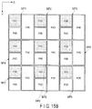
- FIG. 18A is an illustration for explanation of a reference pixel and a pixel to be corrected according to Example 2.
- FIG. 18B is an illustration for explanation of a reference pixel and two pixels to be corrected according to Example 2.
- FIG. 18C is an illustration for explanation of a reference pixel and three pixels to be corrected according to Example 2.
- FIG. 18D is an illustration for explanation of a reference pixel and four pixels to be corrected according to Example 2.
- FIG. 19A is an illustration for explanation of a reference pixel and a pixel to be corrected according to Example 3.
- FIG. 19B is an illustration for explanation of a reference pixel and two pixels to be corrected according to Example 3.
- FIG. 19C is an illustration for explanation of a reference pixel and three pixels to be corrected according to Example 3.
- FIG. 19D is an illustration for explanation of a reference pixel and four pixels to be corrected according to Example 3.
- FIG. 20A is an illustration for explanation of a reference pixel and a pixel to be corrected according to Example 4.
- FIG. 20B is an illustration for explanation of a reference pixel and two pixels to be corrected according to Example 4.
- FIG. 20C is an illustration for explanation of a reference pixel and three pixels to be corrected according to Example 4.
- FIG. 20D is an illustration for explanation of a reference pixel and four pixels to be corrected according to Example 4.
- FIG. 21A is an illustration for explanation of a reference pixel and four pixels to be corrected according to Example 5.
- FIG. 21B is an illustration for explanation of a reference pixel and two pixels to be corrected according to Example 5.
- FIG. 21C is an illustration for explanation of a reference pixel and two pixels to be corrected according to Example 5.
- a display device includes a plurality of main pixels including a first main pixel disposed in intersecting first and second directions, wherein the first main pixel comprises a first sub-pixel displaying a first color, a second sub-pixel displaying a second color different from the first color, and a third sub-pixel displaying a third color different from the first and second colors, the first and second sub-pixels are arranged in the second direction, the first and third sub-pixels are arranged in the first direction, and the second and third sub-pixels are arranged in the first direction, and each of the first and second sub-pixels has a first length in the first direction, and the third sub-pixel has a second length smaller than the first length in the first direction.
- a display device includes a plurality of main pixels including a first main pixel and a second main pixel adjacent to each other, disposed in intersecting first and second directions, wherein the first main pixel comprises first to third sub-pixels, the third sub-pixel has an area larger than areas of the first and second sub-pixels, the first and second sub-pixels are arranged in the second direction, the first and third sub-pixels are arranged in the first direction, and the second and third sub-pixels are arranged in the first direction, the second main pixel comprises fourth to sixth sub-pixels, the sixth sub-pixel has an area larger than areas of the fourth and fifth sub-pixels, the fourth and fifth sub-pixels are arranged in the second direction, the fourth and sixth sub-pixels are arranged in the first direction, and the fifth and sixth sub-pixels are arranged in the first direction, any one of the first to third sub-pixels is a reference pixel and any one of the fourth to sixth sub-pixels is a correcting target pixel to
- a display device includes a plurality of main pixels including a first main pixel disposed in intersecting first and second directions, wherein the first main pixel comprises first to third sub-pixels, the third sub-pixel has an area larger than areas of the first and second sub-pixels, the first and second sub-pixels are arranged in the second direction, the first and third sub-pixels are arranged in the first direction, and the second and third sub-pixels are arranged in the first direction, any one of the first to third sub-pixels is a correcting target pixel to be corrected, input data to drive the correcting target pixel on a first luminance level is converted into corrected data of a second luminance level different from the first luminance level, and the correcting target pixel is driven based on the corrected data.
- a liquid crystal display device is explained as an example of the display device.
- the major configuration explained in the present embodiment can also be applied to a self-luminous display device comprising an organic electroluminescent display element, and the like, an electronic paper display device comprising an electrophoretic element, and the like, a display device employing micro-electromechanical systems (MEMS), or a display device employing electrochromism.
- MEMS micro-electromechanical systems
- the display device of the embodiments can be used for, for example, various devices such as a smartphone, a tablet terminal, a mobile telephone terminal, a personal computer, a TV receiver, a vehicle-mounted device, and a game console.
- FIG. 1 is a perspective view showing a structural example of a display device DSP according to the embodiments.
- a first direction X and a second direction Y intersect each other, and a third direction Z intersects the first direction X and the second direction Y.
- the first direction X, the second direction Y, and the third direction Z are orthogonal to each other but may intersect at an angle other than 90 degrees.
- a direction facing a tip side of an arrow indicating the third direction Z is called an upper direction (or simply upwardly), and a direction facing a side opposite to the tip of the arrow is called a lower direction (or simply downwardly).
- An observation position at which the display device DSP is observed is assumed to be located on the tip side of the arrow indicating the third direction Z, and viewing from the observation position toward the X-Y plane defined by the first direction X and the second direction Y is called a planar view.
- the display device DSP comprises a display panel PNL, an IC chip 1 , a flexible substrate 2 and the like.
- the display panel PNL implies a liquid crystal display panel, which comprises a first substrate SUB 1 , a second substrate SUB 2 , and a liquid crystal layer (a liquid crystal layer LC explained later).
- the second substrate SUB 2 is opposed to the first substrate SUB 1 .
- the display panel PNL includes a display area DA on which an image is displayed and a frame-shaped non-display area NDA surrounding the display area DA.
- the display panel PNL also includes a plurality of main pixels MP arrayed in a matrix in the first direction X and the second direction Y in the display area DA.
- the display panel PNL of the embodiments may be a transmissive display panel comprising a transmissive display function of displaying an image by allowing the light from the lower surface side of the first substrate SUB 1 to be selectively transmitted, a reflective display panel comprising a reflective display function of displaying an image by allowing the light from the upper surface side of the second substrate SUB 2 to be selectively transmitted, or a transflective display panel comprising both of the transmissive display function and the reflective display function.
- the IC chip 1 and the flexible substrate 2 are connected to the first substrate SUB 1 .
- the flexible substrate 2 connects the display panel PNL and an external circuit board 3 .
- Each of the IC chip 1 , the flexible substrate 2 , and the circuit board 3 functions as a signal supply source configured to supply a signal necessary to display the image to the display panel PNL.
- the IC chip 1 , the flexible substrate 2 , and the circuit board 3 are not necessarily required in the display device DSP of the embodiments.
- FIG. 2 is a diagram showing a structural example of the display device DSP according to the embodiments.
- the display device DSP comprises a signal processor 4 and a driver 5 .
- the signal processor 4 and the driver 5 are provided in any one of the signal supply sources shown in FIG. 1 .
- input data for example, RGB data
- the signal processor 4 executes predetermined data conversion and outputs the data to the driver 5 .
- the driver 5 comprises a signal line drive circuit SD, a scanning line drive circuit GD, and the like.
- the driver 5 controls driving of the display area DA, based on various signals from the signal processor 4 .
- the display area DA includes a plurality of main pixels MP, a plurality of scanning lines G (G 1 to Gn), a plurality of signal lines S (S 1 to Sm), and the like.
- the main pixels MP are arrayed in a matrix in the first direction X and the second direction Y.
- the scanning lines G are spaced apart and arranged in the second direction Y.
- Each of the scanning lines G is electrically connected to the scanning line drive circuit GD.
- the signal lines S are spaced apart and arranged in the first direction X.
- Each of the signal lines S is electrically connected to the signal line drive circuit SD.
- Each main pixel MP comprises, for example, three sub-pixels Pa, Pb, and Pc.
- the sub-pixels Pa and Pb are arranged in the second direction Y, and each of the sub-pixels is located between the scanning lines G 1 and G 2 and between the signal lines S 1 and S 2 .
- the sub-pixels Pa and Pc are arranged in the first direction X and the sub-pixels Pb and Pc are also arranged in the first direction X.
- the sub-pixel Pc is located between the scanning lines G 1 and G 2 and between the signal lines S 2 and S 3 .
- the sub-pixel Pa displays a first color
- the sub-pixel Pb displays a second color different from the first color
- the sub-pixel Pc displays a third color different from the first color and the second color.
- the sub-pixel Pa comprises a switching element SWa and a pixel electrode PEa.
- the switching element SWa is electrically connected to the scanning line G 1 and the signal line S 1 .
- the pixel electrode PEa is electrically connected to the switching element SWa.
- the sub-pixel Pb comprises a switching element SWb and a pixel electrode PEb.
- the switching element SWb is electrically connected to the scanning line G 2 and the signal line S 2 .
- the pixel electrode PEb is electrically connected to the switching element SWb.
- the sub-pixel Pc comprises a switching element SWc and a pixel electrode PEc.
- the switching element SWc is electrically connected to the scanning line G 1 and the signal line S 3 .
- the pixel electrode PEc is electrically connected to the switching element SWc.
- two scanning lines and three signal lines are allocated to one main pixel MP.
- the other main pixels P have similar configuration.
- FIG. 3 is a cross-sectional view showing a structural example of a first substrate SUB 1 shown in FIG. 1 .
- a structural example of the first substrate SUB 1 including the switching element SWa and the pixel electrode PEa of the sub-pixel Pa shown in FIG. 2 will be explained.
- any one of a display mode using a lateral electric field approximately parallel to the main substrate surface, a display mode using a longitudinal electric field approximately perpendicular to the main substrate surface, a display mode using an inclined electric field angled with respect to the main substrate surface, and a display mode using a combination of these display modes can be employed.
- the main substrate surface indicates a surface parallel to the X-Y plane defined by the first direction X and the second direction Y shown in FIG. 1 .
- the first substrate SUB 1 in the example illustrated has a configuration corresponding to a fringe field switching (FFS) mode which is one of the display modes using the lateral electric field.
- FFS fringe field switching
- the first substrate SUB 1 includes a first insulating substrate 10 , a first insulating film 11 , a second insulating film 12 , a third insulating film 13 , a fourth insulating film 14 , a fifth insulating film 15 , a switching element SWa, a pixel electrode PEa, a common electrode CE, a first alignment film AL 1 , and the like.
- the first insulating substrate 10 is formed of a glass substrate or resin substrate having a light transmitting property.
- the switching element SWa is formed in, for example, a top-gate structure, but may be formed in a bottom-gate structure.
- the switching element SWa is composed of a double-gate thin-film transistor, but may be composed of a single-gate thin-film transistor.
- the first insulating film 11 is formed on the first insulating substrate 10 .
- a semiconductor layer SC of the switching element SWa is formed on the first insulating film 11 .
- the semiconductor layer SC is formed of, for example, polycrystalline silicon, but may be formed of amorphous silicon, an oxide semiconductor, or the like.
- the second insulating film 12 is formed on the first insulating film 11 and the semiconductor layer SC.
- the scanning line G 1 is formed on the second insulating film 12 and opposed to the semiconductor layer SC at two parts.
- the third insulating film 13 is formed on the scanning line G 1 and the second insulating film 12 .
- the signal line S 1 and a relay electrode RE 1 are formed on the third insulating film 13 .
- the signal line S 1 is in contact with the semiconductor layer SC through a contact hole CH 11 which penetrates the second insulating film 12 and the third insulating film 13 .
- the relay electrode RE is in contact with the semiconductor layer SC through a contact hole CH 12 which penetrates the second insulating film 12 and the third insulating film 13 .
- the fourth insulating film 14 is formed on the third insulating film 13 , the source line S 1 , and the relay electrode RE.
- the common electrode CE is formed on the fourth insulating film 14 .
- the fifth insulating film 15 is formed on the fourth insulating film 14 and the common electrode CE.
- the first insulating film 11 , the second insulating film 12 , the third insulating film 13 , and the fifth insulating film 15 are formed of, for example, an inorganic material such as a silicon nitride (SiN) or a silicon oxide (SiO).
- the fourth insulating film 14 is formed of, for example, an organic material such as an acrylic resin.
- the pixel electrode PEa is formed on the fifth insulating film 15 .
- the pixel electrode PEa is in contact with the relay electrode RE through a contact hole CH 13 which penetrates the fourth insulating film 14 and the fifth insulating film 15 .
- the common electrode CE and the pixel electrode PEa are formed of, for example, a transparent conductive material such as indium tin oxide (ITO) or indium zinc oxide (IZO).
- the first alignment film AL 1 is formed on the fifth insulating film 15 and the pixel electrode PEa.
- the first alignment film AL 1 is formed of, for example, a material having a horizontal alignment property.
- FIG. 4 is a cross-sectional view showing the structural example of the display panel PNL shown in FIG. 1 .
- a structural example of the display panel PNL including the signal lines S 1 and S 2 and the pixel electrode PEa shown in FIG. 2 will be explained.
- the signal lines S 1 and S 2 , the common electrode CE, the pixel electrode PEa, the first insulating film 11 , the second insulating film 12 , the third insulating film 13 , the fourth insulating film 14 , the fifth insulating film 15 , and the first alignment film AL 1 are located between the first insulating substrate 10 and the liquid crystal layer LC.
- the signal lines S 1 and S 2 are located between the third insulating film 13 and the fourth insulating film 14 .
- the common electrode CE is located between the fourth insulating film 14 and the fifth insulating film 15 .
- the pixel electrode PEa is located between the fifth insulating film 15 and the first alignment film ALL
- the pixel electrode PEa includes a slit SL directly above the common electrode CE.
- the common electrode CE is located not only between the signal lines S 1 and S 2 , but also directly above the signal lines S 1 and S 2 .
- the second substrate SUB 2 includes a second insulating substrate 20 , a light-shielding layer BM, a color filter CF, an overcoat layer OC, a second alignment film AL 2 , and the like.
- the second insulating substrate 20 is a transparent glass substrate or resin substrate, similarly to the first insulating substrate 10 .
- the light-shielding layer BM, the color filter CF, the overcoat layer OC, and the second alignment film AL 2 are located between the second insulating substrate 20 and the liquid crystal layer LC.
- the light-shielding layer BM is formed at a position opposed to the signal lines S 1 and S 2 .
- the light-shielding layer BM is also formed at a position opposed to the scanning lines and the switching elements, though not illustrated in the drawing.
- the color filter CF includes a red color filter CFR, a green color filter CFG, and a blue color filter CFB.
- the red color filter CFR is disposed in a sub-pixel (PXR) displaying a red color.
- the green color filter CFG is disposed in a sub-pixel (PXG) displaying a green color.
- the blue color filter CFB is disposed in a sub-pixel (PXB) displaying a blue color.
- the green color filter CFG is formed at a position opposed to the pixel electrode PEa.
- An end portion of each of the color filters CFR, CFG, and CFB overlaps the light-shielding layer BM.
- the color filters CFR, CFG, and CFB are formed of colored resin materials.
- the color filter CF is formed on the second substrate SUB 2 , but may be formed on the first substrate SUB 1 .
- the overcoat layer OC covers the color filter layer CF.
- the overcoat layer OC is formed of a transparent resin material.
- the second alignment film AL 2 is formed on a side of the overcoat layer OC, which is opposed to the first substrate SUB 1 .
- the second alignment film AL 2 is formed of a material having a horizontal alignment property, similarly to the first alignment film AL 1 .
- the liquid crystal layer LC is held between the first substrate SUB 1 and the second substrate SUB 2 and is in contact with the first alignment film AL 1 and the second alignment film AL 2 .
- the liquid crystal layer LC is constituted by a liquid crystal material having a negative dielectric anisotropy or a liquid crystal material having a positive dielectric anisotropy.
- the first optical element OD 1 is disposed on a side opposite to the side of the first substrate SUB 1 which is opposed to the liquid crystal layer LC.
- the second optical element OD 2 is disposed on a side opposite to the side of the second substrate SUB 2 which is opposed to the liquid crystal layer LC.
- the first optical element OD 1 comprises a polarizer PL 1 and the second optical element OD 2 comprises a polarizer PL 2 .
- Each of the first optical element OD 1 and the second optical element OD 2 may comprise other optical elements such as a retardation film.
- both of the pixel electrode PE and the common electrode CE are disposed on the first substrate SUB 1 , in the display mode using the lateral electric field.
- the pixel electrode PE is disposed on the first substrate SUB 1 while the common electrode CE is disposed on the second substrate SUB 2 .
- FIG. 5 is a cross-sectional view showing another structural example of the display panel PNL shown in FIG. 1 .
- the structural example shown in FIG. 5 is different from the structural example in FIG. 4 with respect to a feature that the pixel electrode PEa is located between the first insulating substrate 10 and the common electrode CE. The only differences from the structural example shown in FIG. 4 are explained.
- the pixel electrode PEa is located on the fourth insulating film 14 and covered with the fifth insulating film 15 .
- the pixel electrode PEa is formed in a flat plate shape and does not include a slit.
- the common electrode CE is located on the fifth insulating film 15 and covered with the first alignment film ALL
- the common electrode CE includes slits SL directly above the pixel electrode PEa.
- FIG. 6 is an illustration showing an example of pixel array in the display area DA shown in FIG. 2 .
- main pixels MP 1 to MP 9 are illustrated in the drawing.
- the main pixels MP 1 to MP 3 are arranged in this order in the first direction X
- the main pixels PX 4 to MP 6 are arranged in this order in the first direction X
- the main pixels PX 7 to MP 9 are arranged in this order in the first direction X.
- the main pixels MP 1 , MP 4 , and MP 7 are arranged in this order in the second direction Y
- the main pixels PX 2 , MP 5 , and MP 8 are arranged in this order in the second direction Y
- the main pixels PX 3 , PX 6 , and MP 9 are arranged in this order in the second direction Y.
- the main pixel MP 1 comprises sub-pixels P 1 to P 3 .
- the main pixel MP 2 comprises sub-pixels P 4 to P 6 .
- the main pixel MP 3 comprises sub-pixels P 7 to P 9 .
- the sub-pixels P 1 , P 4 , and P 7 are configured similarly to the sub-pixel Pa shown in FIG. 2 .
- the sub-pixels P 2 , P 5 , and P 8 are configured similarly to the sub-pixel Pb shown in FIG. 2 .
- the sub-pixels P 3 , P 6 , and P 9 are configured similarly to the sub-pixel Pc shown in FIG. 2 .
- the sub-pixels P 1 , P 6 , and P 8 are sub-pixels PXG displaying green and each of the sub-pixels comprises the green color filter CFG shown in FIG. 4 .
- the sub-pixels P 2 , P 4 , and P 9 are sub-pixels PXB displaying blue and each of the sub-pixels comprises the blue color filter CFB shown in FIG. 4 .
- the sub-pixels P 3 , P 5 , and P 7 are sub-pixels PXR displaying red and each of the sub-pixels comprises the red color filter CFR shown in FIG. 4 .
- the green sub-pixels PXG are drawn with hatch lines sloped right-downward
- the blue sub-pixels PXB are drawn with hatch lines sloped right-upward
- the red sub-pixels PXR are drawn with longitudinal lines.
- green, blue, and red correspond to the first color, the second color, and third color, respectively, but the colors are not limited to this combination.
- the main pixels MP 5 and MP 9 have the same configuration as the main pixel MP 1 .
- the main pixels MP 6 and MP 7 have the same configuration as the main pixel MP 2 .
- the main pixels MP 4 and MP 8 have the same configuration as the main pixel MP 3 .
- the main pixel MP 1 corresponding to the first main pixel is noted, the sub-pixel P 1 corresponds to the first sub-pixel, the sub-pixel P 2 corresponds to the second sub-pixel, and the sub-pixel P 3 corresponds to the third sub-pixel.
- the main pixel MP 1 comprises sub-pixels P 1 to P 3 of different colors.
- the sub-pixel P 2 is adjacent to the sub-pixel P 1
- the sub-pixel P 3 is adjacent to the sub-pixels P 1 and P 2 .
- the main pixel MP 1 has a length Lx in the first direction X, and a length Ly in the second direction Y.
- the length Lx is equal to the length Ly
- the main pixel MP 1 is formed in a square shape.
- Each of the sub-pixels P 1 and P 2 has a length L 1 in the first direction X
- the sub-pixel P 3 has a length L 2 in the first direction X.
- the length L 1 is equal to the length L 2 .
- a sum of the lengths of the sub-pixels P 1 and P 2 in the second direction Y is equal to the length of the sub-pixel P 3 in the second direction Y.
- each of the sub-pixels P 1 and P 2 has a length L 3 in the first direction X
- the sub-pixel P 3 has a length L 4 in the second direction Y.
- the length L 4 is larger than the length L 3 and is approximately twice the length L 3 .
- the sub-pixels P 1 and P 2 have the substantially same shape and the same area.
- the length L 1 is substantially equal to the length L 3
- the sub-pixels P 1 and P 2 are formed in a substantially square shape.
- the length L 4 is substantially twice the length L 2
- the sub-pixel P 3 is formed in a rectangular shape elongated in the second direction Y.
- An area of the sub-pixel P 3 is larger than an area of the sub-pixel P 1 and is substantially twice the area of the sub-pixel P 1 .
- the sub-pixel P 3 has the largest area, and the sub-pixels P 1 and P 2 have the smallest area.
- FIG. 7 is an illustration for explanation of an example of coloring at the time of displaying an oblique line in a display area DA including main pixels shown in FIG. 6 .
- a potion colored in black does not contribute to the display (or corresponds to a region displaying black)
- the sub-pixel PXR represented by longitudinal lines displays red.
- the portion contributing to the display includes a number of sub-pixels PXB and PXG having larger areas, and the area of the sub-pixel PXR is smaller than the areas of the sub-pixels PXB and PXG.
- the blue and green display areas are larger than the red display area in the portion contributing to the display, and the portion is entirely colored in cyan.
- white balance is degraded and the portions of arrows 71 and 72 illustrated in the drawing can easily be recognized visually to be colored in cyan.
- FIG. 8 is an illustration for explanation of an example of coloring at the time of displaying a checkered pattern in the display area DA including the main pixels shown in FIG. 6 .
- a portion colored in black is a region displaying black
- a portion represented by hatch lines sloped right-downward is the green sub-pixel PXG
- a portion represented by hatch lines sloped right-upward is the blue sub-pixel PXB
- a portion represented by longitudinal lines is the red sub-pixel PXR displaying red, similarly to FIG. 7 .
- a red display area is larger than the blue and green display areas at the portions of arrows 81 and 84 illustrated, and the portions seem entirely colored in red.
- the blue display area is larger than the red and green display areas at a portion of arrow 82 , and the portion seems entirely colored in cyan.
- the green display area is larger than the red and blue display areas at a portion of arrow 83 , and the portion seems entirely colored in yellow.
- the stripe pattern of red, green, and blue can easily be recognized visually.
- FIG. 9 is an illustration showing another example of pixel array in the display area DA shown in FIG. 2 .
- the example shown in FIG. 9 is different from the example shown in FIG. 6 with respect to a feature that a difference in area between the sub-pixel having the largest area and the sub-pixel having the smallest area in each main pixel MP is set to be smaller than twice.
- the main pixel MP 1 corresponding to the first main pixel is noted, the sub-pixel P 1 corresponds to the first sub-pixel displaying a first color, the sub-pixel P 2 corresponds to the second sub-pixel displaying a second color, and the sub-pixel P 3 corresponds to the third sub-pixel displaying a third color.
- the first color, the second color, and the third color are different colors and, for example, the first color is green, the second color is blue, and the third color is red but the colors are not limited to the combination of these colors.
- the main pixel MP 1 has a length Lx in the first direction X, and a length Ly in the second direction Y.
- the length Lx is substantially equal to the length Ly
- the main pixel MP 1 is formed in a square shape.
- the sub-pixels P 1 and P 2 are arranged in the second direction Y
- the sub-pixels P 1 and P 3 are arranged in the first direction X
- the sub-pixels P 2 and P 3 are arranged in the first direction X.
- Each of the sub-pixels P 1 and P 2 has a length L 1 in the first direction X
- the sub-pixel P 3 has a length L 2 in the first direction X.
- the length L 2 is shorter than the length L 1 .
- a sum of the lengths of the sub-pixels P 1 and P 2 in the second direction Y is substantially equal to the length of the sub-pixel P 3 in the second direction Y.
- each of the sub-pixels P 1 and P 2 has a length L 3 in the first direction X
- the sub-pixel P 3 has a length L 4 in the second direction Y.
- the length L 4 is larger than the length L 3 and is approximately twice the length L 3 .
- the sub-pixels P 1 and P 2 have the same shape and the same area.
- the length L 3 is shorter than the length L 1 , and the sub-pixels P 1 and P 2 are formed in a rectangular shape elongated in the first direction X.
- the length L 4 is larger than the length L 2 , and the sub-pixel P 3 is formed in a rectangular shape elongated in the second direction Y.
- An area A 3 of the sub-pixel P 3 is greater than 0.5 times and less than twice an area A 1 of the sub-pixel P 1 .
- the difference between the area A 1 of each of the sub-pixels P 1 and P 2 and the area A 3 of the sub-pixel P 3 can be reduced as compared with the pixel array shown in FIG. 6 . If the area A 3 is greater than 0.5 times and smaller than once the area A 1 , each of the sub-pixels P 1 and P 2 has the largest area and the sub-pixel P 3 has the smallest area, in the main pixel MP 1 . If the area A 3 is once the area A 1 , the sub-pixels P 1 to P 3 have the same areas in the main pixel MP 1 .
- each of the sub-pixels P 1 and P 2 has the smallest area and the sub-pixel P 3 has the largest area, in the main pixel MP 1 .
- the condition for making the difference in area smallest is that the area A 3 is once the area A 1 , and is desirable with respect to a feature of obtaining preferable white balance in one main pixel.
- the main pixel MP 2 corresponding to the second main pixel comprises the sub-pixel P 4 corresponding to the fourth sub-pixel, the sub-pixel P 5 corresponding to the fifth sub-pixel, and the sub-pixel P 6 corresponding to the sixth sub-pixel.
- Each of the sub-pixels P 4 and P 5 has a length L 5 in the first direction X
- the sub-pixel P 6 has a length L 6 in the first direction X.
- the length L 6 is shorter than the length L 5 .
- the main pixel MP 3 corresponding to the third main pixel comprises the sub-pixel P 7 corresponding to the seventh sub-pixel, the sub-pixel P 8 corresponding to the eighth sub-pixel, and the sub-pixel P 9 corresponding to the ninth sub-pixel.
- Each of the sub-pixels P 7 and P 8 has a length L 7 in the first direction X
- the sub-pixel P 9 has a length L 8 in the first direction X.
- the length L 8 is shorter than the length L 7 .
- the lengths L 5 and L 7 are equal to the length L 1
- the lengths L 6 and L 8 are equal to the length L 2 .
- Each of the sub-pixels P 4 , P 5 , P 7 , and P 8 has an area equal to the area of the sub-pixel P 1
- Each of the sub-pixels P 9 and P 9 has an area equal to the area of the sub-pixel P 3 .
- the sub-pixels P 6 and P 8 are the sub-pixels displaying the first color, similarly to the sub-pixel P 1 .
- the sub-pixels P 4 and P 9 are the sub-pixels displaying the second color, similarly to the sub-pixel P 2 .
- the sub-pixels P 5 and P 7 are the sub-pixels displaying the third color, similarly to the sub-pixel P 3 .
- the main pixels MP 5 and MP 9 have the same configuration as the main pixel MP 1 .
- the main pixels MP 6 and MP 7 have the same configuration as the main pixel MP 2 .
- the main pixels MP 4 and MP 8 have the same configuration as the main pixel MP 3 .
- Nine main pixels MP 1 to MP 9 illustrated in the drawing constitute one display block. Such display blocks are repeatedly arranged in the first direction X and the second direction Y to constitute the display area DA.
- the degradation of the display quality in displaying a specific pattern can be suppressed by using the pixel array shown in FIG. 9 , as compared with use of the pixel array shown in FIG. 6 .
- the difference in area between the sub-pixel having the largest area and the sub-pixel having the smallest area can be reduced to less than twice in the main pixel comprising three sub-pixels of different colors. For this reason, difference in area contributing to the display becomes small in the sub-pixels of the respective colors.
- the difference among the red component, green component, and the blue component becomes small in one main pixel.
- the hue in one main pixel therefore becomes closer to white as compared with the pixel array shown in FIG. 6 .
- the difference in hue is also reduced in adjacent main pixels.
- FIG. 10 is an illustration for explanation of a displayed state of displaying an oblique line in the display area DA including main pixels shown in FIG. 9 .
- the portion contributing to the display includes the sub-pixels PXR, PXG, and PXB, and their areas are substantially equal to each other. For this reason, coloring to add a color different from white can be reduced. In other words, when the illustrated pattern is displayed, white balance is maintained and coloring of the portions of arrows 71 and 72 illustrated in the drawing can not easily be recognized visually.
- FIG. 11 is an illustration for explanation of a displayed state of displaying a checkered pattern in the display area DA including the main pixels shown in FIG. 9 .
- the areas of the sub-pixels PXR, PXG, and PXB are substantially equal to each other at the portion contributing to the display. For this reason, when the illustrated pattern is displayed, coloring of the portions of arrows 81 to 84 illustrated in the drawing can be reduced and the stripe pattern of a specific color is not easily recognized visually.
- the degradation in display quality can be thus suppressed.
- FIG. 12 is an illustration showing an example of a structural example applicable to the pixel array shown in FIG. 9 .
- a region including the main pixels MP 1 , MP 2 , MP 4 , and MP 5 is illustrated.
- the signal lines S 1 to S 7 are arranged in this order in the first direction X.
- an interval between the signal lines S 1 and S 2 is larger than an interval between the signal lines S 2 and S 3
- the interval between the signal lines S 2 and S 3 is larger than an interval between the signal lines S 3 and S 4 .
- the scanning lines G 1 to G 3 are arranged in this order in the second direction Y. The intervals between the adjacent scanning lines are equal to each other.
- the main pixel MP 1 comprises a pixel electrode PE 1 disposed in the sub-pixel P 1 , a pixel electrode PE 2 disposed in the sub-pixel P 2 , and a pixel electrode PE 3 disposed in the sub-pixel P 3 .
- the pixel electrodes PE 1 and PE 2 are arranged in the second direction Y, and each of the pixel electrodes is located between the scanning lines G 1 and G 2 and between the signal lines S 1 and S 2 .
- the pixel electrodes PE 1 and PE 3 are arranged in the first direction X while sandwiching the signal line S 2 , and the pixel electrodes PE 2 and PE 3 are arranged in the first direction X while sandwiching the signal line S 2 .
- the pixel electrode PE 3 is located between the scanning lines G 1 and G 2 and between the signal lines S 2 and S 3 .
- the area of the sub-pixel corresponds to the installation area of the pixel electrode disposed in each sub-pixel.
- a switching element SW 1 is electrically connected with the scanning line G 1 and the signal line S 1 .
- the pixel electrode PE 1 is electrically connected with the switching element SW 1 .
- a switching element SW 2 is electrically connected with the scanning line G 2 and the signal line S 2 .
- the pixel electrode PE 2 is electrically connected with the switching element SW 2 .
- a switching element SW 3 is electrically connected with the scanning line G 1 and the signal line S 3 .
- the pixel electrode PE 3 is electrically connected with the switching element SW 3 .
- the main pixel MP 2 has the same configuration as the main pixel MP 1 .
- the pixel electrode PE 4 of the sub-pixel P 4 is electrically connected with the switching element SW 4
- the pixel electrode PE 5 of the sub-pixel P 5 is electrically connected with the switching element SW 5
- the pixel electrode PE 6 of the sub-pixel P 6 is electrically connected with the switching element SW 6 .
- the pixel electrodes PE 3 and PE 4 are arranged in the first direction X while sandwiching the signal lines S 3 and S 4
- the pixel electrodes PE 3 and PE 5 are arranged in the first direction X while sandwiching the signal lines S 3 and S 4 .
- FIG. 13 is an illustration showing another example of the pixel array in the display area DA shown in FIG. 2 .
- the example shown in FIG. 13 is different from the example in FIG. 9 with respect to a feature that the sub-pixels P 4 and P 7 are the sub-pixels displaying the first color similarly to the sub-pixel P 1 , the sub-pixels P 5 and P 8 are the sub-pixels displaying the second color similarly to the sub-pixel P 2 , and the sub-pixels P 6 and P 9 are the sub-pixels displaying the third color similarly to the sub-pixel P 3 .
- all the main pixels MP 1 to MP 9 have the same configuration.
- the first color is green
- the second color is blue
- the third color is red.
- the third color may be blue, and the first color and the second color may be red and green, respectively.
- the third color may be green, and the first color and the second color may be red and blue, respectively.
- the area of the sub-pixel P 3 is equal to the area of each of the sub-pixels P 1 and P 2 .
- the areas contributing to the display in three sub-pixels of different colors thereby become equal to each other in one main pixel, and the white balance can be maintained.
- the red component is more than the blue and green components in the main pixel MP 1
- the green component is more than the red and blue components in the main pixel MP 2
- a difference in hue is generated between the adjacent main pixels.
- the red component, the green component, and the blue component are substantially equal to each other in each main pixel, and no difference in hue is generated between the adjacent main pixels. For this reason, the same color arrangement can be implemented in all the main pixels and the pixel array can be simplified.
- FIG. 14 is an illustration for explanation of a method of driving at least one sub-pixel based on corrected data.
- the illustrated main pixel MP can correspond to any one of the main pixels MP 1 to MP 9 shown in FIG. 6 .
- the illustrated main pixel MP corresponds to the main pixel MP 1 in FIG. 6
- the illustrated sub-pixels Pa, Pb, and Pc correspond to the sub-pixels P 1 to P 3 in FIG. 6 , respectively.
- Each of the sub-pixels Pa, Pb, and Pc may be a correcting target pixel to be corrected as driven based on corrected data.
- the input data for driving the sub-pixels Pa, Pb, and Pc at predetermined luminance levels are denoted by a, b, and c, respectively, and the input data (a, b, c) in the drawing indicates input data input to the signal processor 4 to drive the main pixel MP.
- the signal processor 4 converts the input data (a, b, c) into corrected data (Ca, Cb, Cc) and outputs the corrected data to the driver 5 .
- the input data and the corrected data is data corresponding to a gradation value, for example, values in a range from 0 to 255.
- the signal line drive circuit SD generates video signals (Da, Db, Dc) of a voltage value corresponding to the gradation value, based on the corrected data (Ca, Cb, Cc).
- the signal line drive circuit SD outputs the video signal Da to the signal line S 1 electrically connected to the sub-pixel Pa and outputs the video signal Dc to the signal line S 3 electrically connected to the sub-pixel Pc, at timing of supplying an ON signal to the scanning line G 1 .
- the signal line drive circuit SD outputs the video signal Db to the signal line S 2 electrically connected to the sub-pixel Pb at timing of supplying an ON signal to the scanning line G 2 .
- the video signals Da, Db, and Dc are thereby written to the sub-pixels Pa, Pb, and Pc.
- ⁇ is a parameter to determine the rate for converting the luminance level
- ⁇ and ⁇ are parameters determined arbitrarily in accordance with requirement for correction of the gamma property at conversion of the luminance level.
- the sub-pixel Pc having the largest area in the main pixel MP is assumed to be the correcting target pixel and to be driven with the corrected data Cc of the second luminance level lower than the first luminance level at which the sub-pixel Pc is driven with the input data c.
- the input data (a, b, c) is assumed to be (127, 127, 127) as the gradation values.
- each of the sub-pixels Pa and Pb is driven based on the corrected data that is the same as the input data while the sub-pixel is driven based on the corrected data of the gradation values smaller than the input data.
- a second luminance level in driving the sub-pixel Pc at gradation value 115 corresponds to a level which is 0.8 times the first luminance level in driving the sub-pixel at gradation value 127.
- the red sub-pixel PXR in each of the main pixels MP 1 , MP 5 , and MP 9 the red sub-pixel PXR in each of the main pixels MP 1 , MP 5 , and MP 9
- the green sub-pixel PXG in each of the main pixels MP 2 , MP 6 , and MP 7 the blue sub-pixel PXB in each of the main pixels MP 3 , MP 4 , and MP 8 are driven at the second luminance level lower than the first luminance level, as shown in FIG. 15A .
- the sub-pixel Pa having the smallest area in the main pixel MP is assumed to be the correcting target pixel and to be driven with the corrected data Ca of the second luminance level higher than the first luminance level at which the sub-pixel Pa is driven with the input data a.
- the input data (a, b, c) is assumed to be (127, 127, 127) as the gradation values.
- each of the sub-pixels Pb and Pc is driven based on the corrected data that is the same as the input data while the sub-pixel Pa is driven based on the corrected data of the gradation values larger than the input data.
- the second luminance level in driving the sub-pixel Pa at gradation value 133 corresponds to a level which is 1.1 times the first luminance level in driving the sub-pixel at gradation value 127.
- the sub-pixel Pb may be correcting target pixels and each of ⁇ b, ⁇ b, ⁇ b may be set at a value other than 1.
- the green sub-pixel PXG in each of the main pixels MP 1 , MP 5 , and MP 9 the green sub-pixel PXG in each of the main pixels MP 1 , MP 5 , and MP 9
- the red sub-pixel PXR in each of the main pixels MP 3 , MP 4 , and MP 8 are driven at the second luminance level higher than the first luminance level, as shown in FIG. 15B .
- all the sub-pixels Pa, Pb, and Pc in the main pixel MP are assumed to be the correcting target pixels
- the sub-pixels Pa and Pb are assumed to be driven with the corrected data Ca and Cb of the second luminance level higher than the first luminance level at which the sub-pixels Pa and Pb are driven with the input data a and b
- the sub-pixel Pc is assumed to be driven with the corrected data Cc of the second luminance level lower than the first luminance level at which the sub-pixel Pc is driven with the input data c.
- the input data (a, b, c) is assumed to be (127, 127, 127) as the gradation values.
- each of the sub-pixels Pa and Pb is driven based on the corrected data that is larger than the input data while the sub-pixel Pc is driven based on the corrected data of the gradation values smaller than the input data.
- the second luminance level in driving the sub-pixel Pa at gradation value 133 corresponds to a level which is 1.1 times the first luminance level in driving the sub-pixel at gradation value 127.
- the second luminance level in driving the sub-pixel Pb at gradation value 138 corresponds to a level which is 1.2 times the first luminance level in driving the sub-pixel at gradation value 127.
- a second luminance level in driving the sub-pixel Pc at gradation value 115 corresponds to a level which is 0.8 times the first luminance level in driving the sub-pixel at gradation value 127.
- the red sub-pixel PXR in each of the main pixels MP 1 , MP 5 , and MP 9 the red sub-pixel PXR in each of the main pixels MP 1 , MP 5 , and MP 9
- the green sub-pixel PXG in each of the main pixels MP 2 , MP 6 , and MP 7 the blue sub-pixel PXB in each of the main pixels MP 3 , MP 4 , and MP 8 are driven at the second luminance level lower than the first luminance level, as shown in FIG. 15C .
- the green sub-pixel PXG in each of the main pixels MP 1 , MP 5 , and MP 9 , the blue sub-pixel PXB in each of the main pixels MP 2 , MP 6 , and MP 7 , and the red sub-pixel PXR in each of the main pixels MP 3 , MP 4 , and MP 8 are driven at the second luminance level higher than the first luminance level.
- the blue sub-pixel PXB in each of the main pixels MP 1 , MP 5 , and MP 9 , the red sub-pixel PXR in each of the main pixels MP 2 , MP 6 , and MP 7 , and the green sub-pixel PXG in each of the main pixels MP 3 , MP 4 , and MP 8 are driven at the second luminance level higher than the first luminance level.
- the parameters ⁇ , ⁇ , and ⁇ are defined when the input data is converted into the corrected but, more simply, the gradation values of the corrected data may be obtained by setting ⁇ and ⁇ of Expressions (1) to (3) at 1 and multiplying the gradation values of the input data by ⁇ .
- ⁇ can be set in a range of, for example, larger than 0.5 and smaller than 2.0.
- ⁇ a and ⁇ b are set in a range of larger than 1 and smaller than 2 while ⁇ c is set in a range of larger than 0.5 and smaller than 1.
- the parameter values can be arbitrarily selected in the signal processor 4 in accordance with the displayed pattern and the like.
- the difference in luminance among the sub-pixels Pa, Pb, and Pc can be reduced by driving the sub-pixel Pc with the corrected data to make the luminance lower than that in a case where the sub-pixel Pc is driven with the input data.
- undesired coloring can be reduced even in displaying the pattern as shown in FIG. 7 and FIG. 8 .
- coloring can be simultaneously reduced by driving the sub-pixels Pa and Pb with the corrected data to make the luminance higher than that in a case where the sub-pixels are driven with the input data.
- the difference in luminance among the sub-pixels Pa, Pb, and Pc can be further reduced by driving the sub-pixel Pc with the corrected data which makes the luminance lower and driving the sub-pixels Pa and Pb with the corrected data which makes the luminance higher. For this reason, undesired coloring can be further reduced.
- FIG. 16 is an illustration for explanation of a method of driving adjacent main pixels, based on the corrected data.
- Correspondence of the illustrated main pixels to the main pixels shown in FIG. 6 is as follows.
- a main pixel MPn ⁇ w corresponds to the main pixel MP 2
- a main pixel MPn ⁇ 1 corresponds to the main pixel MP 4
- a main pixel MPn corresponds to the main pixel MP 5
- a main pixel MPn+1 corresponds to the main pixel MP 6
- a main pixel MPn+w corresponds to the main pixel MP 8 .
- each of the main pixels MPn ⁇ w, MPn+w, MPn ⁇ 1, and MPn+1 can be a second main pixel adjacent to the first main pixel.
- any one of the sub-pixels of the main pixel MPn can be a reference pixel, and at least one of the sub-pixels of the main pixels MPn ⁇ w, MPn+w, MPn ⁇ 1, and MPn+1 can be a correcting target pixel driven based on the corrected data.
- the signal processor 4 converts the input data (a, b, c) into the corrected data (Ca, Cb, Cc) and outputs the corrected data to the driver 5 , similarly to the above-explained examples.
- input data an ⁇ w, bn ⁇ w, cn ⁇ w
- Can ⁇ w, Cbn ⁇ w, Ccn ⁇ w is converted into corrected data (Can ⁇ w, Cbn ⁇ w, Ccn ⁇ w).
- Input data (an ⁇ 1, bn ⁇ 1, cn ⁇ 1) to drive sub-pixels Pan ⁇ 1, Pbn ⁇ 1, and Pcn ⁇ 1 of the main pixel MPn ⁇ 1 is converted into corrected data (Can ⁇ 1, Cbn ⁇ 1, Ccn ⁇ 1).
- Input data (an, bn, cn) to drive sub-pixels Pan, Pbn, and Pcn of the main pixel MPn is converted into corrected data (Can, Cbn, Ccn).
- Input data (an+1, bn+1, cn+1) to drive sub-pixels Pan+1, Pbn+1, and Pcn+1 of the main pixel MPn+1 is converted into corrected data (Can+1, Cbn+1, Ccn+1).
- Input data (an+w, bn+w, cn+w) to drive sub-pixels Pan+w, Pbn+w, and Pcn+w of the main pixel MPn+w is converted into corrected data (Can+w, Cbn+w, Ccn+w).
- Example 1 the sub-pixel Pan (or Pbn) having the smallest area in the main pixel MPn is assumed to be the reference pixel, the sub-pixel Pcn ⁇ 1 having the largest area in the main pixel MPn ⁇ 1 is assumed to be the correcting target pixel, and the sub-pixel Pcn ⁇ 1 is assumed to be driven with the corrected data Ccn ⁇ 1 of third luminance level different from the second luminance level at which the sub-pixel Pcn ⁇ 1 is driven with second input data cn ⁇ 1. If the reference pixel and the correcting target pixel explained here are applied to the pixel array shown in FIG.
- the green sub-pixel PXG of the main pixel MP 5 corresponds to the reference pixel
- the blue sub-pixel PXB of the main pixel MP 4 correspond to the correcting target pixels, as shown in FIG. 17A .
- the reference pixel is represented by lateral lines and the correcting target pixel is represented by dots.
- First input data to drive the main pixel MPn is represented as (an, bn, cn).
- Second input data to drive the main pixel MPn ⁇ 1 is represented as (an ⁇ 1, bn ⁇ 1, cn ⁇ 1).
- Corrected data of the second input data is represented as (Can ⁇ 1, Cbn ⁇ 1, Ccn ⁇ 1).
- Can ⁇ 1 is consider to be equal to an ⁇ 1 and Cbn ⁇ 1 is considered to be equal to bn ⁇ 1.
- An example of a transformation for obtaining the corrected data Ccn ⁇ 1 is as follows.
- Ccn ⁇ 1 (( cn ⁇ 1 ⁇ cn ⁇ 1 * ⁇ cn ⁇ 1) ⁇ cn ⁇ 1 +( an ⁇ an * ⁇ an ) ⁇ an )/2 (4)
- the first input data (an, bn, cn) is considered to be (127, 127, 127) as gradation values
- the second input data (an ⁇ 1, bn ⁇ 1, cn ⁇ 1) is considered to be (0, 0, 0) as gradation values.
- the sub-pixels Pan ⁇ 1, Pbn ⁇ 1, and Pcn ⁇ 1 of the main pixel MPn ⁇ 1 are driven with the corrected data Can ⁇ 1, Cbn ⁇ 1, and Ccn ⁇ 1, respectively.
- each of the sub-pixels Pan ⁇ 1 and Pbn ⁇ 1 is driven based on the corrected data that is the same as the second input data while the sub-pixel Pcn ⁇ 1 is driven based on the corrected data of the gradation values larger than the input data.
- the sub-pixels Pan, Pbn, and Pcn of the main pixel MPn are driven with the first input data an, bn, and cn, respectively.
- acn, acn ⁇ 1, ycn, and ycn ⁇ 1 may be set at 1 and ⁇ cn and ⁇ cn ⁇ 1 may be arbitrarily set within a range of larger than or equal to 0.5 and smaller than 1. For example, if ⁇ cn ⁇ 1 is set at 1 and ⁇ cn is set at 0.8, the corrected data Ccn ⁇ 1 is 50 according to Expression (4) explained above.
- the sub-pixel Pan of the main pixel MPn is considered as the reference pixel and the sub-pixel Pcn ⁇ 1 of the main pixel MPn ⁇ 1 is considered as the correcting target pixel in the above example, but the sub-pixels are not limited to the example.
- the sub-pixel Pan of the main pixel MPn is considered as the reference pixel
- the sub-pixel Pcn ⁇ w of the main pixel MPn ⁇ w and the sub-pixel Pcn+w of the main pixel MPn+w are considered as the correcting target pixels.
- the green sub-pixel PXG of the main pixel MP 5 corresponds to the reference pixel
- the green sub-pixel PXG of the main pixel MP 2 and the blue sub-pixel PXB of the main pixel MP 8 correspond to the correcting target pixels, as shown in FIG. 17B .
- the input data (an, bn, cn) is (224, 224, 224) as gradation values
- the input data (an ⁇ w, bn ⁇ w, cn ⁇ w) is (63, 63, 63) as gradation values
- the input data is (an+w, bn+w, cn+w) is (127, 127, 127) as gradation values.
- Parameters in Expression (5) are as follows.
- the sub-pixels Pan ⁇ w, Pbn ⁇ w, and Pcn ⁇ w of the main pixel MPn ⁇ w are driven with the corrected data Can ⁇ w, Cbn ⁇ w, and Ccn ⁇ w, respectively.
- each of the sub-pixels Pan ⁇ w and Pbn ⁇ w is driven based on the corrected data that is the same as the second input data while the sub-pixel Pcn ⁇ w is driven based on the corrected data of the gradation values larger than the input data.
- the sub-pixels Pan+w, Pbn+w, and Pcn+w of the main pixel MPn+w are driven with the corrected data Can+w, Cbn+w, and Ccn+w, respectively.
- each of the sub-pixels Pan+w and Pbn+w is driven based on the corrected data that is the same as the second input data while the sub-pixel Pcn+w is driven based on the corrected data of the gradation values larger than the input data.
- the sub-pixels Pan, Pbn, and Pcn of the main pixel MPn are driven with the input data an, bn, and cn, respectively.
- the sub-pixel Pan of the main pixel MPn is considered as the reference pixel
- the sub-pixel Pcn ⁇ 1 of the main pixel MPn ⁇ 1 is considered as the correcting target pixel.
- Another example of the transformation for obtaining the corrected data Ccn ⁇ 1 driving the sub-pixel pcn ⁇ 1 is as follows.
- Ccn ⁇ 1 (( cn ⁇ 1)+ an ) ⁇ 2 (11)
- Ccn ⁇ 1 (( cn ⁇ 1)+( cn+ 1)+ an ) ⁇ 3
- Ccn ⁇ 1 (( cn ⁇ 1)+( cn+ 1)+( cn+w )+ an ) ⁇ 4
- Ccn ⁇ 1 (( cn ⁇ 1)+( cn+ 1)+( cn+w )+( cn ⁇ w )+ an ) ⁇ 5
- Expression (11) corresponds to an example of obtaining the corrected data by considering luminance of the main pixel MPn including the reference pixel Pan and luminance of the main pixel MPn ⁇ 1 adjacent to the main pixel MPn.
- the correcting target pixel may be any one of the green sub-pixel PXG (sub-pixel Pcn ⁇ w) of the main pixel MP 2 , the blue sub-pixel PXB (sub-pixel Pcn ⁇ 1) of the main pixel MP 4 , the green sub-pixel PXG (sub-pixel Pcn+1) of the main pixel MP 6 , and the blue sub-pixel PXB (sub-pixel Pcn+w) of the main pixel MP 8 as shown in FIG. 17A .
- Expression (12) corresponds to an example of obtaining the corrected data by considering luminance of the main pixel MPn including the reference pixel Pan and luminance of two main pixels MPn ⁇ 1 and MPn+1 adjacent to the main pixel MPn.
- the corrected data Ccn+1 of the sub-pixel Pn+1 can also be obtained based on Expression (12).
- the correcting target pixel may be a combination of any two sub-pixels of the green sub-pixel PXG (sub-pixel Pcn ⁇ w) of the main pixel MP 2 , the blue sub-pixel PXB (sub-pixel Pcn ⁇ 1) of the main pixel MP 4 , the green sub-pixel PXG (sub-pixel Pcn+1) of the main pixel MP 6 , and the blue sub-pixel PXB (sub-pixel Pcn+w) of the main pixel MP 8 , as shown in FIG. 17B .
- Expression (13) corresponds to an example of obtaining the corrected data by considering luminance of the main pixel MPn including the reference pixel Pan and luminance of three main pixels MPn ⁇ 1, MPn+1 and MPn+w adjacent to the main pixel MPn.
- the corrected data Ccn+1 of the sub-pixel Pn+1 and the corrected data Ccn+w of the sub-pixel Pn+w can also be obtained based on Expression (13).
- the green sub-pixel PXG of the main pixel MP 5 corresponds to the reference pixel
- the blue sub-pixel PXB of the main pixel MP 4 , the green sub-pixel PXG of the main pixel MP 6 , and the blue sub-pixel PXB of the main pixel MP 8 correspond to the correcting target pixels, as shown in FIG. 17C .
- the correcting target pixel may be a combination of any three sub-pixels of the green sub-pixel PXG (sub-pixel Pcn ⁇ w) of the main pixel MP 2 , the blue sub-pixel PXB (sub-pixel Pcn ⁇ 1) of the main pixel MP 4 , the green sub-pixel PXG (sub-pixel Pcn+1) of the main pixel MP 6 , and the blue sub-pixel PXB (sub-pixel Pcn+w) of the main pixel MP 8 , as shown in FIG. 17C .
- Expression (14) corresponds to an example of obtaining the corrected data by considering luminance of the main pixel MPn including the reference pixel Pan and luminance of all of four main pixels MPn ⁇ 1, MPn+1, MPn+w and MPn ⁇ w adjacent to the main pixel MPn.
- the corrected data Ccn+1 of the sub-pixel Pn+1, the corrected data Ccn+w of the sub-pixel Pn+w and the corrected data Ccn ⁇ w of the sub-pixel Pn ⁇ w can also be obtained based on Expression (14).
- the green sub-pixel PXG of the main pixel MP 5 corresponds to the reference pixel
- the green sub-pixel PXG of the main pixel MP 2 , the blue sub-pixel PXB of the main pixel MP 4 , the green sub-pixel PXG of the main pixel MP 6 , and the blue sub-pixel PXB of the main pixel MP 8 correspond to the correcting target pixels, as shown in FIG. 17D .
- Example 2 the sub-pixel Pcn having the largest area in the main pixel MPn is assumed to be the reference pixel, the sub-pixel Pcn ⁇ 1 having the largest area in the main pixel MPn ⁇ 1 is assumed to be the correcting target pixel, and the sub-pixel Pcn ⁇ 1 is assumed to be driven with the corrected data Ccn ⁇ 1.
- An example of a simplified transformation for obtaining the corrected data Ccn ⁇ 1 is as follows.
- the red sub-pixel PXR of the main pixel MP 5 corresponds to the reference pixel
- the blue sub-pixel PXB of the main pixel MP 4 corresponds to the correcting target pixel, as shown in FIG. 18A
- the correcting target pixel may be any one of the green sub-pixel PXG (sub-pixel Pcn ⁇ w) of the main pixel MP 2 , the blue sub-pixel PXB (sub-pixel Pcn ⁇ 1) of the main pixel MP 4 , the green sub-pixel PXG (sub-pixel Pcn+1) of the main pixel MP 6 , and the blue sub-pixel PXB (sub-pixel Pcn+w) of the main pixel MP 8 as shown in FIG. 18A .
- the red sub-pixel PXR of the main pixel MP 5 corresponds to the reference pixel
- the blue sub-pixel PXB of the main pixel MP 4 and the green sub-pixel PXG of the main pixel MP 6 correspond to the correcting target pixels, as shown in FIG. 18B .
- the correcting target pixel may be a combination of any two sub-pixels of the green sub-pixel PXG (sub-pixel Pcn ⁇ w) of the main pixel MP 2 , the blue sub-pixel PXB (sub-pixel Pcn ⁇ 1) of the main pixel MP 4 , the green sub-pixel PXG (sub-pixel Pcn+1) of the main pixel MP 6 , and the blue sub-pixel PXB (sub-pixel Pcn+w) of the main pixel MP 8 , as shown in FIG. 18B .
- the red sub-pixel PXG of the main pixel MP 5 corresponds to the reference pixel
- the blue sub-pixel PXB of the main pixel MP 4 , the green sub-pixel PXG of the main pixel MP 6 , and the blue sub-pixel PXB of the main pixel MP 8 correspond to the correcting target pixels as shown in FIG. 18C .
- the correcting target pixel may be a combination of any three sub-pixels of the green sub-pixel PXG (sub-pixel Pcn ⁇ w) of the main pixel MP 2 , the blue sub-pixel PXB (sub-pixel Pcn ⁇ 1) of the main pixel MP 4 , the green sub-pixel PXG (sub-pixel Pcn+1) of the main pixel MP 6 , and the blue sub-pixel PXB (sub-pixel Pcn+w) of the main pixel MP 8 as shown in FIG. 18C .
- the red sub-pixel PXR of the main pixel MP 5 corresponds to the reference pixel
- the green sub-pixel PXG of the main pixel MP 2 , the blue sub-pixel PXB of the main pixel MP 4 , the green sub-pixel PXG of the main pixel MP 6 , and the blue sub-pixel PXB of the main pixel MP 8 correspond to the correcting target pixels, as shown in FIG. 18D .
- Example 3 the sub-pixel Pan (or Pbn) having the smallest area in the main pixel MPn is assumed to be the reference pixel, the sub-pixel Pbn ⁇ 1 (or Pan ⁇ 1) having the smallest area in the main pixel MPn ⁇ 1 is assumed to be the correcting target pixel, and the sub-pixel Pbn ⁇ 1 is assumed to be driven with the corrected data Cbn ⁇ 1.
- An example of a simplified transformation for obtaining the corrected data Cbn ⁇ 1 is as follows.
- Cbn ⁇ 1 (( bn ⁇ 1)+ an ) ⁇ 2 (31)
- Cbn ⁇ 1 (( bn ⁇ 1)+( bn+ 1)+ an ) ⁇ 3
- Cbn ⁇ 1 (( bn ⁇ 1)+( bn+ 1)+( bn+w )+ an ) ⁇ 4
- Cbn ⁇ 1 (( bn ⁇ 1)+( bn+ 1)+( bn+w )+ an ) ⁇ 5 (34)
- (bn ⁇ 1) can be replaced with (an ⁇ 1)
- (bn+1) can be replaced with (an+1)
- (bn+w) can be replaced with (an+w)
- (bn ⁇ w) can be replaced with (an ⁇ w)
- an can be replaced with bn.
- the corrected data Can ⁇ 1 can also be obtained based on Expression (31).
- the corrected data Can ⁇ 1, Can+1, and Cbn+1 can also be obtained based on Expression (32).
- the corrected data Can ⁇ 1, Can+1, Cbn+1, Can+w, and Cbn+w can also be obtained based on Expression (33).
- the corrected data Can ⁇ 1, Can+1, Cbn+1, Can+w, Cbn+w, Can ⁇ w, and Cbn ⁇ w can also be obtained based on Expression (34).
- the green sub-pixel PXG of the main pixel MP 5 corresponds to the reference pixel
- the green sub-pixel PXG of the main pixel MP 4 corresponds to the correcting target pixel, as shown in FIG. 19A .
- the correcting target pixel may be any one of the blue sub-pixel PXB (sub-pixel Pan ⁇ w) and the red sub-pixel PXR (sub-pixel Pbn ⁇ w) of the main pixel MP 2 , the red sub-pixel PXR (sub-pixel Pan ⁇ 1) and the green sub-pixel PXG (sub-pixel Pbn ⁇ 1) of the main pixel MP 4 , the blue sub-pixel PXB (sub-pixel Pan+1) and the red sub-pixel PXR (sub-pixel Pbn+1) of the main pixel MP 6 , and the red sub-pixel PXR (sub-pixel Pan+w) and the green sub-pixel PXG (sub-pixel Pbn+w) of the main pixel MP 8 as shown in FIG. 19A .
- the green sub-pixel PXG of the main pixel MP 5 corresponds to the reference pixel
- the green sub-pixel PXG of the main pixel MP 4 and the red sub-pixel PXR of the main pixel MP 6 correspond to the correcting target pixels, as shown in FIG. 19B .
- the correcting target pixel may be a combination of any two sub-pixels of the blue sub-pixel PXB (sub-pixel Pan ⁇ w) and the red sub-pixel PXR (sub-pixel Pbn ⁇ w) of the main pixel MP 2 , the red sub-pixel PXR (sub-pixel Pan ⁇ 1) and the green sub-pixel PXG (sub-pixel Pbn ⁇ 1) of the main pixel MP 4 , the blue sub-pixel PXB (sub-pixel Pan+1) and the red sub-pixel PXR (sub-pixel Pbn+1) of the main pixel MP 6 , and the red sub-pixel PXR (sub-pixel Pan+w) and the green sub-pixel PXG (sub-pixel Pbn+w) of the main pixel MP 8 as shown in FIG. 19B .
- the green sub-pixel PXG of the main pixel MP 5 corresponds to the reference pixel
- the green sub-pixel PXG of the main pixel MP 4 , the red sub-pixel PXR of the main pixel MP 6 , and the green sub-pixel PXG of the main pixel MP 8 correspond to the correcting target pixels, as shown in FIG. 19C .
- the correcting target pixel may be a combination of any three sub-pixels of the blue sub-pixel PXB (sub-pixel Pan ⁇ w) and the red sub-pixel PXR (sub-pixel Pbn ⁇ w) of the main pixel MP 2 , the red sub-pixel PXR (sub-pixel Pan ⁇ 1) and the green sub-pixel PXG (sub-pixel Pbn ⁇ 1) of the main pixel MP 4 , the blue sub-pixel PXB (sub-pixel Pan+1) and the red sub-pixel PXR (sub-pixel Pbn+1) of the main pixel MP 6 , and the red sub-pixel PXR (sub-pixel Pan+w) and the green sub-pixel PXG (sub-pixel Pbn+w) of the main pixel MP 8 as shown in FIG. 19C .
- the green sub-pixel PXG of the main pixel MP 5 corresponds to the reference pixel
- the red sub-pixel PXR of the main pixel MP 2 , the green sub-pixel PXG of the main pixel MP 4 , the red sub-pixel PXR of the main pixel MP 6 , and the green sub-pixel PXG of the main pixel MP 8 correspond to the correcting target pixels, as shown in FIG. 19D .
- Example 4 the sub-pixel Pcn having the largest area in the main pixel MPn is assumed to be the reference pixel, the sub-pixel Pbn ⁇ 1 (or Pan ⁇ 1) having the smallest area in the main pixel MPn ⁇ 1 is assumed to be the correcting target pixel, and the sub-pixel Pbn ⁇ 1 is assumed to be driven with the corrected data Cbn ⁇ 1.
- An example of a simplified transformation for obtaining the corrected data Cbn ⁇ 1 is as follows.
- Cbn ⁇ 1 (( bn ⁇ 1)+ cn ) ⁇ 2 (41)
- Cbn ⁇ 1 (( bn ⁇ 1)+( bn+ 1)+ cn ) ⁇ 3 (42)
- Cbn ⁇ 1 (( bn ⁇ 1)+( bn+ 1)+( bn+w )+ cn ) ⁇ 4 (43)
- Cbn ⁇ 1 (( bn ⁇ 1)+( bn+ 1)+( bn+w )+( bn ⁇ w )+ cn ) ⁇ 5 (44)
- Example 4 too, the replacement explained in Example 3 can be executed and the other corrected data can also be obtained based on Expressions (41) to (44).
- the red sub-pixel PXR of the main pixel MP 5 corresponds to the reference pixel
- the green sub-pixel PXG of the main pixel MP 4 corresponds to the correcting target pixel, as shown in FIG. 20A .
- the correcting target pixel may be any one of the blue sub-pixel PXB (sub-pixel Pan ⁇ w) and the red sub-pixel PXR (sub-pixel Pbn ⁇ w) of the main pixel MP 2 , the red sub-pixel PXR (sub-pixel Pan ⁇ 1) and the green sub-pixel PXG (sub-pixel Pbn ⁇ 1) of the main pixel MP 4 , the blue sub-pixel PXB (sub-pixel Pan+1) and the red sub-pixel PXR (sub-pixel Pbn+1) of the main pixel MP 6 , and the red sub-pixel PXR (sub-pixel Pan+w) and the green sub-pixel PXG (sub-pixel Pbn+w) of the main pixel MP 8 as shown in FIG. 20A .
- the red sub-pixel PXR of the main pixel MP 5 corresponds to the reference pixel
- the green sub-pixel PXG of the main pixel MP 4 and the red sub-pixel PXR of the main pixel MP 6 correspond to the correcting target pixels, as shown in FIG. 20B .
- the correcting target pixel may be a combination of any two sub-pixels of the blue sub-pixel PXB (sub-pixel Pan ⁇ w) and the red sub-pixel PXR (sub-pixel Pbn ⁇ w) of the main pixel MP 2 , the red sub-pixel PXR (sub-pixel Pan ⁇ 1) and the green sub-pixel PXG (sub-pixel Pbn ⁇ 1) of the main pixel MP 4 , the blue sub-pixel PXB (sub-pixel Pan+1) and the red sub-pixel PXR (sub-pixel Pbn+1) of the main pixel MP 6 , and the red sub-pixel PXR (sub-pixel Pan+w) and the green sub-pixel PXG (sub-pixel Pbn+w) of the main pixel MP 8 as shown in FIG. 20B .
- the red sub-pixel PXR of the main pixel MP 5 corresponds to the reference pixel
- the green sub-pixel PXG of the main pixel MP 4 , the red sub-pixel PXR of the main pixel MP 6 , and the green sub-pixel PXG of the main pixel MP 8 correspond to the correcting target pixels, as shown in FIG. 20C .
- the correcting target pixel may be a combination of any three sub-pixels of the blue sub-pixel PXB (sub-pixel Pan ⁇ w) and the red sub-pixel PXR (sub-pixel Pbn ⁇ w) of the main pixel MP 2 , the red sub-pixel PXR (sub-pixel Pan ⁇ 1) and the green sub-pixel PXG (sub-pixel Pbn ⁇ 1) of the main pixel MP 4 , the blue sub-pixel PXB (sub-pixel Pan+1) and the red sub-pixel PXR (sub-pixel Pbn+1) of the main pixel MP 6 , and the red sub-pixel PXR (sub-pixel Pan+w) and the green sub-pixel PXG (sub-pixel Pbn+w) of the main pixel MP 8 as shown in FIG. 20C .
- the red sub-pixel PXR of the main pixel MP 5 corresponds to the reference pixel
- the red sub-pixel PXR of the main pixel MP 2 , the green sub-pixel PXG of the main pixel MP 4 , the red sub-pixel PXR of the main pixel MP 6 , and the green sub-pixel PXG of the main pixel MP 8 correspond to the correcting target pixels, as shown in FIG. 20D .
- any one of the sub-pixels in the main pixel MPn is assumed to be the reference pixel
- any one of the sub-pixels in the adjacent main pixel MPn ⁇ 1 is assumed to be the correcting target pixel
- the reference pixel and the correcting target pixel are assumed to be the sub-pixels having the same color.
- the sub-pixel Pcn having the largest area in the main pixel MPn is assumed to be the reference pixel
- the sub-pixel Pan ⁇ 1 having the smallest area in the main pixel MPn ⁇ 1 is assumed to be the correcting target pixel.
- both of the sub-pixels Pcn and Pan ⁇ 1 are sub-pixels displaying red.
- An example of a simplified transformation for obtaining the corrected data Can ⁇ 1 of the sub-pixel Pan ⁇ 1 is as follows.
- Can ⁇ 1 (( bn ⁇ w )+( an ⁇ 1)+( bn+ 1)+( an+w )+ cn ) ⁇ 5 (51)
- Expression (51) corresponds to an example of obtaining the corrected data by considering luminance of the reference pixel Pcn, and sub-pixels which are red similarly to the reference pixel Pcn, in four main pixels MPn ⁇ 1, MPn+1, MPn+w and MPn ⁇ w adjacent to the main pixel MPn.
- the corrected data Cbn ⁇ w, Cbn+1, Can+w, and Ccn can also be obtained based on Expression (51).
- the red sub-pixel PXR of the main pixel MP 5 corresponds to the reference pixel
- the red sub-pixel PXR of each of the main pixels MP 2 , MP 4 , MP 6 , and MP 8 corresponds to the correcting target pixels, as shown in FIG. 21A .
- both of the sub-pixels Pan and Pbn ⁇ 1 are sub-pixels displaying green.
- An example of a simplified transformation for obtaining the corrected data Cbn ⁇ 1 of the sub-pixel Pbn ⁇ 1 is as follows.
- Cbn ⁇ 1 (( bn ⁇ 1)+( bn+w )+ an ) ⁇ 3 (52)
- Expression (52) corresponds to an example of obtaining the corrected data by considering luminance of the reference pixel Pan, and sub-pixels which are green similarly to the reference pixel Pan, in four main pixels MPn ⁇ 1, MPn+1, MPn+w and MPn ⁇ w adjacent to the main pixel MPn.
- the corrected data Cbn+w and Can can also be obtained based on Expression (52).
- an can be replaced with bn in Expression (52).
- the reference pixel can be replaced with the blue sub-pixel.
- (bn ⁇ 1) is replaced with (an+1) while (bn+w) is replaced with (an ⁇ w).
- the green sub-pixel PXG of the main pixel MP 5 corresponds to the reference pixel
- the green sub-pixel PXG of each of the main pixels MP 4 and MP 8 corresponds to the correcting target pixel, as shown in FIG. 21B .
- both of the sub-pixels Pbn and Pcn ⁇ 1 are sub-pixels displaying blue.
- An example of a simplified transformation for obtaining the corrected data Ccn ⁇ 1 of the sub-pixel Pcn ⁇ 1 is as follows.
- Ccn ⁇ 1 (( cn ⁇ 1)+( cn+w )+ bn ) ⁇ 3 (53)
- Expression (53) corresponds to an example of obtaining the corrected data by considering luminance of the reference pixel Pbn, and sub-pixels which are blue similarly to the reference pixel Pbn, in four main pixels MPn ⁇ 1, MPn+1, MPn+w and MPn ⁇ w adjacent to the main pixel MPn.
- the corrected data CCn+w and CBn can also be obtained based on Expression (53).
- bn can be replaced with an in Expression (53).
- the reference pixel can be replaced with the green sub-pixel.
- (cn ⁇ 1) is replaced with (cn+1) while (cn+w) is replaced with (cn ⁇ w).
- the blue sub-pixel PXB of the main pixel MP 5 corresponds to the reference pixel
- the blue sub-pixel PXB of each of the main pixels MP 2 and MP 6 corresponds to the correcting target pixel, as shown in FIG. 21C .
- a display device capable of suppressing the degradation in display quality can be provided by the embodiments.
- the present invention is not limited to the embodiments described above but the constituent elements of the invention can be modified in various manners without departing from the spirit and scope of the invention.
- Various aspects of the invention can also be extracted from any appropriate combination of constituent elements disclosed in the embodiments. For example, some of the constituent elements disclosed in the embodiments may be deleted. Furthermore, the constituent elements described in different embodiments may be arbitrarily combined.
Landscapes
- Physics & Mathematics (AREA)
- Engineering & Computer Science (AREA)
- General Physics & Mathematics (AREA)
- Nonlinear Science (AREA)
- Chemical & Material Sciences (AREA)
- Crystallography & Structural Chemistry (AREA)
- Computer Hardware Design (AREA)
- Theoretical Computer Science (AREA)
- Optics & Photonics (AREA)
- Mathematical Physics (AREA)
- Geometry (AREA)
- Liquid Crystal (AREA)
- Devices For Indicating Variable Information By Combining Individual Elements (AREA)
- Control Of Indicators Other Than Cathode Ray Tubes (AREA)
- Electroluminescent Light Sources (AREA)
- Liquid Crystal Display Device Control (AREA)
Abstract
Description
Ca=(a αa *βa)γa (1)
Cb=(b αb *βb)γb (2)
Cc=(c αc *βc)γc (3)
αa=1 βa=1 γa=1
αb=1 βb=1 γb=1
αc=2.2 βc=0.8 γc=(1/2.2)
Corrected data(Ca,Cb,Cc)=(127,127,115)
αa=2.2 βa=1.1 γa=(1/2.2)
αb=1 βb=1 γb=1
αc=1 βc=1 γc=1
Corrected data(Ca,Cb,Cc)=(133,127,127)
αa=2.2 βa=1.1 γa=(1/2.2)
αb=2.2 βb=1.2 γb=(1/2.2)
αc=2.2 βc=0.8 γc=(1/2.2)
Corrected data(Ca,Cb,Cc)=(133,138,115)
Ccn−1=((cn−1αcn−1 *βcn−1)γcn−1+(an αan *βan)γan)/2 (4)
αcn−1=2.2 βcn−1=1.0 γcn−1=(1/2.2)
αan=2.2 βan=0.8 γan=(1/2.2)
Corrected data(Can−1,Cbn−1,Ccn−1)=(0,0,58)
Ccn−w=Ccn+w=((cn−w αcn−w *βcn−w)γcn−w+(cn+w αcn±w *βcn+w)γcn+w+(an αan *βan)γan)/3 (5)
αcn−w=2.2 βcn−w=1.1 γcn−w=(1/2.2)
αcn+w=2.2 βcn+w=1.2 γcn+w=(1/2.2)
αan=2.2 βan=0.8 γan=(1/2.2)
Corrected data(Can−w,Cbn−w,Ccn−w)=(63,63,135)
Corrected data(Can+w,Cbn+w,Ccn+w)=(127,127,135)
Ccn−1=((cn−1)+an)÷2 (11)
Ccn−1=((cn−1)+(cn+1)+an)÷3 (12)
Ccn−1=((cn−1)+(cn+1)+(cn+w)+an)÷4 (13)
Ccn−1=((cn−1)+(cn+1)+(cn+w)+(cn−w)+an)÷5 (14)
Ccn−1=((cn−1)+cn)÷2 (21)
Ccn−1=((cn−1)+(cn+1)+cn)÷3 (22)
Ccn−1=((cn−1)+(cn+1)+(cn+w)+cn)÷4 (23)
Ccn−1=((cn−1)+(cn+1)+(cn+w)+(cn−w)+cn)÷5 (24)
Cbn−1=((bn−1)+an)÷2 (31)
Cbn−1=((bn−1)+(bn+1)+an)÷3 (32)
Cbn−1=((bn−1)+(bn+1)+(bn+w)+an)÷4 (33)
Cbn−1=((bn−1)+(bn+1)+(bn+w)+(bn−w)+an)÷5 (34)
Cbn−1=((bn−1)+cn)÷2 (41)
Cbn−1=((bn−1)+(bn+1)+cn)÷3 (42)
Cbn−1=((bn−1)+(bn+1)+(bn+w)+cn)÷4 (43)
Cbn−1=((bn−1)+(bn+1)+(bn+w)+(bn−w)+cn)÷5 (44)
Can−1=((bn−w)+(an−1)+(bn+1)+(an+w)+cn)÷5 (51)
Cbn−1=((bn−1)+(bn+w)+an)÷3 (52)
Ccn−1=((cn−1)+(cn+w)+bn)÷3 (53)
Claims (16)
Applications Claiming Priority (2)
| Application Number | Priority Date | Filing Date | Title |
|---|---|---|---|
| JP2016-214518 | 2016-11-01 | ||
| JP2016214518A JP2018072676A (en) | 2016-11-01 | 2016-11-01 | Display device |
Publications (2)
| Publication Number | Publication Date |
|---|---|
| US20180122332A1 US20180122332A1 (en) | 2018-05-03 |
| US10540940B2 true US10540940B2 (en) | 2020-01-21 |
Family
ID=62022477
Family Applications (1)
| Application Number | Title | Priority Date | Filing Date |
|---|---|---|---|
| US15/727,931 Active 2038-02-17 US10540940B2 (en) | 2016-11-01 | 2017-10-09 | Display device |
Country Status (2)
| Country | Link |
|---|---|
| US (1) | US10540940B2 (en) |
| JP (1) | JP2018072676A (en) |
Families Citing this family (5)
| Publication number | Priority date | Publication date | Assignee | Title |
|---|---|---|---|---|
| KR20200106589A (en) | 2019-03-04 | 2020-09-15 | 삼성디스플레이 주식회사 | Carrier, apparatus for manufacturing a display apparatus having the same and method for manufacturing a display apparatus |
| CN110738969A (en) * | 2019-10-31 | 2020-01-31 | 云谷(固安)科技有限公司 | Display device and apparatus |
| US11557635B2 (en) | 2019-12-10 | 2023-01-17 | Samsung Display Co., Ltd. | Display device, mask assembly, and apparatus for manufacturing the display device |
| KR20220010622A (en) * | 2020-07-16 | 2022-01-26 | 삼성디스플레이 주식회사 | Display device |
| KR20230108805A (en) * | 2022-01-11 | 2023-07-19 | 삼성디스플레이 주식회사 | Display device and vehicle including display device |
Citations (10)
| Publication number | Priority date | Publication date | Assignee | Title |
|---|---|---|---|---|
| JPH09204156A (en) | 1996-01-25 | 1997-08-05 | Canon Inc | Display device |
| US20050083355A1 (en) | 2003-10-17 | 2005-04-21 | Tadanori Tezuka | Apparatus and method for image-processing, and display apparatus |
| JP2005141209A (en) | 2003-10-17 | 2005-06-02 | Matsushita Electric Ind Co Ltd | Apparatus and method for image-processing, and display apparatus |
| US20050225548A1 (en) | 2004-04-09 | 2005-10-13 | Clairvoyante, Inc | System and method for improving sub-pixel rendering of image data in non-striped display systems |
| US7515122B2 (en) * | 2004-06-02 | 2009-04-07 | Eastman Kodak Company | Color display device with enhanced pixel pattern |
| US20110181633A1 (en) * | 2010-01-28 | 2011-07-28 | Sony Corporation | Driving method for image display apparatus and driving method for image display apparatus assembly |
| US8552635B2 (en) * | 2010-05-26 | 2013-10-08 | Samsung Display Co., Ltd. | Pixel arrangement of an organic light emitting display device |
| US8952374B2 (en) * | 2013-03-25 | 2015-02-10 | Sony Corporation | Display and electronic apparatus |
| JP2016102971A (en) | 2014-11-28 | 2016-06-02 | 株式会社ジャパンディスプレイ | Display device |
| US20160155776A1 (en) | 2014-11-28 | 2016-06-02 | Japan Display Inc. | Display device |
-
2016
- 2016-11-01 JP JP2016214518A patent/JP2018072676A/en active Pending
-
2017
- 2017-10-09 US US15/727,931 patent/US10540940B2/en active Active
Patent Citations (13)
| Publication number | Priority date | Publication date | Assignee | Title |
|---|---|---|---|---|
| JPH09204156A (en) | 1996-01-25 | 1997-08-05 | Canon Inc | Display device |
| US20050083355A1 (en) | 2003-10-17 | 2005-04-21 | Tadanori Tezuka | Apparatus and method for image-processing, and display apparatus |
| JP2005141209A (en) | 2003-10-17 | 2005-06-02 | Matsushita Electric Ind Co Ltd | Apparatus and method for image-processing, and display apparatus |
| JP5227018B2 (en) | 2004-04-09 | 2013-07-03 | 三星ディスプレイ株式會社 | System and method for improving sub-pixel rendering of image data in non-striped display systems |
| US20050225548A1 (en) | 2004-04-09 | 2005-10-13 | Clairvoyante, Inc | System and method for improving sub-pixel rendering of image data in non-striped display systems |
| US7515122B2 (en) * | 2004-06-02 | 2009-04-07 | Eastman Kodak Company | Color display device with enhanced pixel pattern |
| US20110181633A1 (en) * | 2010-01-28 | 2011-07-28 | Sony Corporation | Driving method for image display apparatus and driving method for image display apparatus assembly |
| US8552635B2 (en) * | 2010-05-26 | 2013-10-08 | Samsung Display Co., Ltd. | Pixel arrangement of an organic light emitting display device |
| US8952374B2 (en) * | 2013-03-25 | 2015-02-10 | Sony Corporation | Display and electronic apparatus |
| JP2016102971A (en) | 2014-11-28 | 2016-06-02 | 株式会社ジャパンディスプレイ | Display device |
| US20160155776A1 (en) | 2014-11-28 | 2016-06-02 | Japan Display Inc. | Display device |
| US20160155777A1 (en) | 2014-11-28 | 2016-06-02 | Japan Display Inc. | Display device |
| JP2016102935A (en) | 2014-11-28 | 2016-06-02 | 株式会社ジャパンディスプレイ | Display device |
Also Published As
| Publication number | Publication date |
|---|---|
| JP2018072676A (en) | 2018-05-10 |
| US20180122332A1 (en) | 2018-05-03 |
Similar Documents
| Publication | Publication Date | Title |
|---|---|---|
| US10540940B2 (en) | Display device | |
| US9971188B2 (en) | Display device | |
| US8659725B2 (en) | Pixel structure, liquid crystal display panel and transparent liquid crystal display device | |
| US7554640B2 (en) | LCD device having a set of comb-like electrodes of red, green and blue pixels in a row extending in a first direction and a set of electrodes of a white pixel in the row extending in a second different direction | |
| US8441601B2 (en) | Display apparatus having improved brightness and color reproducibility | |
| US20150214280A1 (en) | Display device | |
| US9978321B2 (en) | Display device and method of driving the same | |
| US10067372B2 (en) | LCD improving color shift at large viewing angle | |
| KR20150130578A (en) | Fringe field liquid crystal display | |
| US9904122B2 (en) | Display device | |
| US10330998B2 (en) | Display device | |
| CN102193241A (en) | Electro-optical display apparatus | |
| US10741617B2 (en) | Pixel structure, array substrate and display device | |
| US9904139B2 (en) | Color filter substrate, display panel and display device | |
| US9841642B2 (en) | Liquid crystal display device | |
| KR20160089572A (en) | Liquid crystal display | |
| US11048133B2 (en) | Liquid crystal display panel and liquid crystal display device including the same | |
| US10317748B2 (en) | Display panels and the array substrates thereof | |
| KR20160081999A (en) | Liquid Crystal Display Device | |
| US10185070B2 (en) | Display device and light source device | |
| US9459508B2 (en) | Display device | |
| US9477020B2 (en) | Display apparatus | |
| US20170003554A1 (en) | Liquid crystal display | |
| CN108196411B (en) | Liquid crystal display panel and display device thereof | |
| US8848150B2 (en) | Liquid crystal display and electronic device |
Legal Events
| Date | Code | Title | Description |
|---|---|---|---|
| FEPP | Fee payment procedure |
Free format text: ENTITY STATUS SET TO UNDISCOUNTED (ORIGINAL EVENT CODE: BIG.); ENTITY STATUS OF PATENT OWNER: LARGE ENTITY |
|
| AS | Assignment |
Owner name: JAPAN DISPLAY INC., JAPAN Free format text: ASSIGNMENT OF ASSIGNORS INTEREST;ASSIGNORS:IKEDA, KOJIRO;KABE, MASAAKI;NAKAOKA, CHIKYU;REEL/FRAME:044575/0111 Effective date: 20170809 |
|
| STPP | Information on status: patent application and granting procedure in general |
Free format text: DOCKETED NEW CASE - READY FOR EXAMINATION |
|
| STPP | Information on status: patent application and granting procedure in general |
Free format text: NON FINAL ACTION MAILED |
|
| STPP | Information on status: patent application and granting procedure in general |
Free format text: RESPONSE TO NON-FINAL OFFICE ACTION ENTERED AND FORWARDED TO EXAMINER |
|
| STPP | Information on status: patent application and granting procedure in general |
Free format text: NOTICE OF ALLOWANCE MAILED -- APPLICATION RECEIVED IN OFFICE OF PUBLICATIONS |
|
| STPP | Information on status: patent application and granting procedure in general |
Free format text: PUBLICATIONS -- ISSUE FEE PAYMENT VERIFIED |
|
| STCF | Information on status: patent grant |
Free format text: PATENTED CASE |
|
| MAFP | Maintenance fee payment |
Free format text: PAYMENT OF MAINTENANCE FEE, 4TH YEAR, LARGE ENTITY (ORIGINAL EVENT CODE: M1551); ENTITY STATUS OF PATENT OWNER: LARGE ENTITY Year of fee payment: 4 |