US10481218B2 - Providing information about a target object in a formatted output signal - Google Patents
Providing information about a target object in a formatted output signal Download PDFInfo
- Publication number
- US10481218B2 US10481218B2 US15/695,109 US201715695109A US10481218B2 US 10481218 B2 US10481218 B2 US 10481218B2 US 201715695109 A US201715695109 A US 201715695109A US 10481218 B2 US10481218 B2 US 10481218B2
- Authority
- US
- United States
- Prior art keywords
- speed
- information
- response
- diagnostic
- target object
- Prior art date
- Legal status (The legal status is an assumption and is not a legal conclusion. Google has not performed a legal analysis and makes no representation as to the accuracy of the status listed.)
- Active, expires
Links
- 230000004044 response Effects 0.000 claims description 59
- 238000000034 method Methods 0.000 claims description 51
- 230000005291 magnetic effect Effects 0.000 claims description 35
- 230000005540 biological transmission Effects 0.000 claims description 12
- 230000005355 Hall effect Effects 0.000 claims description 6
- 238000012544 monitoring process Methods 0.000 claims description 6
- 230000005641 tunneling Effects 0.000 claims description 5
- 230000008569 process Effects 0.000 description 37
- 238000012545 processing Methods 0.000 description 25
- 230000008859 change Effects 0.000 description 9
- 238000004590 computer program Methods 0.000 description 9
- 230000006870 function Effects 0.000 description 6
- 238000011084 recovery Methods 0.000 description 6
- 238000010586 diagram Methods 0.000 description 5
- 230000003287 optical effect Effects 0.000 description 4
- 230000035945 sensitivity Effects 0.000 description 4
- 239000000758 substrate Substances 0.000 description 4
- 230000007704 transition Effects 0.000 description 4
- 238000004891 communication Methods 0.000 description 3
- 230000005294 ferromagnetic effect Effects 0.000 description 3
- 239000004065 semiconductor Substances 0.000 description 3
- 230000008901 benefit Effects 0.000 description 2
- 238000001514 detection method Methods 0.000 description 2
- WPYVAWXEWQSOGY-UHFFFAOYSA-N indium antimonide Chemical compound [Sb]#[In] WPYVAWXEWQSOGY-UHFFFAOYSA-N 0.000 description 2
- 239000000463 material Substances 0.000 description 2
- 238000012360 testing method Methods 0.000 description 2
- 238000012546 transfer Methods 0.000 description 2
- JBRZTFJDHDCESZ-UHFFFAOYSA-N AsGa Chemical compound [As]#[Ga] JBRZTFJDHDCESZ-UHFFFAOYSA-N 0.000 description 1
- XUIMIQQOPSSXEZ-UHFFFAOYSA-N Silicon Chemical compound [Si] XUIMIQQOPSSXEZ-UHFFFAOYSA-N 0.000 description 1
- 230000001133 acceleration Effects 0.000 description 1
- 230000002238 attenuated effect Effects 0.000 description 1
- 239000004020 conductor Substances 0.000 description 1
- 230000008878 coupling Effects 0.000 description 1
- 238000010168 coupling process Methods 0.000 description 1
- 238000005859 coupling reaction Methods 0.000 description 1
- -1 e.g. Chemical compound 0.000 description 1
- 238000005516 engineering process Methods 0.000 description 1
- 229910052732 germanium Inorganic materials 0.000 description 1
- GNPVGFCGXDBREM-UHFFFAOYSA-N germanium atom Chemical compound [Ge] GNPVGFCGXDBREM-UHFFFAOYSA-N 0.000 description 1
- 150000002472 indium compounds Chemical class 0.000 description 1
- 230000005381 magnetic domain Effects 0.000 description 1
- 238000004519 manufacturing process Methods 0.000 description 1
- 229910052751 metal Inorganic materials 0.000 description 1
- 239000002184 metal Substances 0.000 description 1
- 230000005855 radiation Effects 0.000 description 1
- 239000000523 sample Substances 0.000 description 1
- 229910052710 silicon Inorganic materials 0.000 description 1
- 239000010703 silicon Substances 0.000 description 1
Images


Classifications
-
- G—PHYSICS
- G01—MEASURING; TESTING
- G01R—MEASURING ELECTRIC VARIABLES; MEASURING MAGNETIC VARIABLES
- G01R33/00—Arrangements or instruments for measuring magnetic variables
- G01R33/02—Measuring direction or magnitude of magnetic fields or magnetic flux
- G01R33/06—Measuring direction or magnitude of magnetic fields or magnetic flux using galvano-magnetic devices
- G01R33/07—Hall effect devices
-
- G—PHYSICS
- G01—MEASURING; TESTING
- G01P—MEASURING LINEAR OR ANGULAR SPEED, ACCELERATION, DECELERATION, OR SHOCK; INDICATING PRESENCE, ABSENCE, OR DIRECTION, OF MOVEMENT
- G01P21/00—Testing or calibrating of apparatus or devices covered by the preceding groups
- G01P21/02—Testing or calibrating of apparatus or devices covered by the preceding groups of speedometers
-
- H—ELECTRICITY
- H03—ELECTRONIC CIRCUITRY
- H03K—PULSE TECHNIQUE
- H03K5/00—Manipulating of pulses not covered by one of the other main groups of this subclass
- H03K5/01—Shaping pulses
- H03K5/08—Shaping pulses by limiting; by thresholding; by slicing, i.e. combined limiting and thresholding
-
- H—ELECTRICITY
- H03—ELECTRONIC CIRCUITRY
- H03K—PULSE TECHNIQUE
- H03K7/00—Modulating pulses with a continuously-variable modulating signal
- H03K7/08—Duration or width modulation ; Duty cycle modulation
-
- G—PHYSICS
- G08—SIGNALLING
- G08B—SIGNALLING OR CALLING SYSTEMS; ORDER TELEGRAPHS; ALARM SYSTEMS
- G08B25/00—Alarm systems in which the location of the alarm condition is signalled to a central station, e.g. fire or police telegraphic systems
- G08B25/01—Alarm systems in which the location of the alarm condition is signalled to a central station, e.g. fire or police telegraphic systems characterised by the transmission medium
- G08B25/04—Alarm systems in which the location of the alarm condition is signalled to a central station, e.g. fire or police telegraphic systems characterised by the transmission medium using a single signalling line, e.g. in a closed loop
- G08B25/045—Alarm systems in which the location of the alarm condition is signalled to a central station, e.g. fire or police telegraphic systems characterised by the transmission medium using a single signalling line, e.g. in a closed loop with sensing devices and central station in a closed loop, e.g. McCullough loop
Definitions
- sensors can be used in various types of devices to measure and monitor properties of systems in a wide variety of different applications.
- sensors have become common in products that rely on electronics in their operation, such as automobile control systems.
- Common examples of automotive applications are the detection of ignition timing from an engine crankshaft and/or camshaft, the detection of wheel speed for anti-lock braking systems and four-wheel steering systems and speed and direction of transmission input and output gears.
- sensors can use serial communication to send data in the form of a stream of pulses or bits over a communication channel or to a computer or other processing system.
- each pulse stream conveys a limited amount of data.
- an integrated circuit includes a sensor.
- the sensor includes a processor configured to provide speed and/or direction of a target object based on the speed of the target object; monitor for diagnostic faults; provide information if a diagnostic fault is detected; monitor for critical faults; and provide information if a critical fault is detected and the sensor recovers from the critical fault.
- a method in another aspect, includes providing speed and/or direction of a target object based on the speed of the target object; monitoring for a diagnostic fault; providing information if the diagnostic fault is detected; monitoring for critical faults; and providing information if a critical fault is detected and a sensor recovers from the critical fault.
- an integrated circuit includes a means to provide speed and/or direction of a target object based on the speed of the target object; monitor for a diagnostic fault; provide information if the diagnostic fault is detected; monitor for critical faults; and provide information if a critical fault is detected and the sensor recovers from the critical fault.
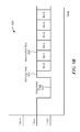
- FIG. 1A is a block diagram of a system having a sensor disposed proximate to a target object
- FIG. 1B is a block diagram of a sensor to generate a formatted output signal
- FIG. 1C is a block diagram of a system having a sensor disposed to sense properties of an environment around the sensor;
- FIG. 2 is a circuit diagram of a system having a sensor and circuitry to detect the formatted output signal provided by the sensor;
- FIGS. 3A to 3C is a flowchart of an example of a process to format an output signal
- FIGS. 4A to 4C are timing windows when a target object is at a low speed
- FIGS. 5A to 5C are timing windows when a target object is at a high speed
- FIG. 6 is a timing window after a critical failure and recovery
- FIG. 7A is diagram of one example of information bits
- FIG. 7B are tables of examples of what the information bits may indicate.
- the formatted output signal may include speed and direction of a target within one pulse.
- the formatted output signal may be configured to only include data bits when there is a diagnostic flag.
- a speed and direction pulse is not directly coupled to diagnostic bit timing. That is, diagnostic information can be communicated at any time a diagnostic flag is detected. In some examples, if both speed and diagnostic information is detected simultaneously then first the speed and direction information is communicated followed by a settling time and then the diagnostic flag and bits are transmitted.
- the formatted output signal may provide diagnostic information after a critical failure.
- the formatted output signal may provide signal integrity information of the sensors front end such as for example, identifying if a signal from a sensor is attenuated, identifying if the signal of the sensor is coupled to noise, identifying if the signal of the sensor is offset and so forth.
- the formatted output signal may be a word of 5-bits+1 parity bit, which allows higher frequencies without truncation.
- none, part or all of the information bits (e.g., diagnostic bits, system integrity bits) may be selected to be received.
- each mode can provide different detail levels of diagnostic information.
- diagnostic flags there can be multiple levels diagnostic errors, for example, soft failures and critical failures.
- the pulse width of the diagnostic flag can be changed to identify the type of diagnostic error.
- the data bits following can provide different data depending on the diagnostic flag type.
- true unrecoverable critical failures can occur and the output would be at or between preset DC threshold(s), identifying an unrecoverable critical failure.
- the final transmitted bit may contain a parity bit.
- the information bits may contain, ASIL (Automotive Safety Integrity Level) diagnostic information, sensor front end signal integrity information, target vibration information, sub-circuit diagnostic information, software algorithm failures/resets.
- ASIL Automotive Safety Integrity Level
- a sensor 2 is disposed proximate a target object 4 .
- the sensor 2 may generate a series of pulses, referred to herein as a pulse train, the characteristics and benefits of which will be described herein.
- the sensor 2 may be the same as or similar to the types described in each of U.S. Pat. No. 6,815,944, filed on Oct. 29, 2002, U.S. Pat. No. 7,026,808, filed on Sep. 23, 2004, U.S. Pat. No. 8,624,588, filed on Jul. 31, 2008, U.S. Pat. No. 9,151,771, filed on Dec. 2, 2013, U.S. Pat. No. 8,994,369, filed on Dec. 2, 2013, and U.S. Pat. No. 8,754,640, filed on Jun. 18, 2012, all of which are incorporated herein by reference in their entireties.
- the term “sensor” is used to describe a circuit that uses a magnetic field sensing element, generally in combination with other circuits. Sensors are used in a variety of applications, including, but not limited to, an angle sensor that senses an angle of a direction of a magnetic field, a current sensor that senses a magnetic field generated by a current carried by a current-carrying conductor, a magnetic switch that senses the proximity of a ferromagnetic object, a rotation detector that senses passing ferromagnetic articles, for example, magnetic domains of a ring magnet or a ferromagnetic target (e.g., gear teeth) where the sensor is used in combination with a back-biased or other magnet, and a sensor that senses a magnetic field density of a magnetic field.
- an angle sensor that senses an angle of a direction of a magnetic field
- a current sensor that senses a magnetic field generated by a current carried by a current-carrying conductor
- a magnetic switch that senses the proximity of
- Signal paths 8 a , 8 b couple the sensor 2 to a receiver 10 .
- the signal paths 8 a , 8 b couple a supply voltage 12 and a reference point (e.g., ground) 14 to the sensor 2 as will be described further herein.
- the signal path 8 is shown provided as a two-wire line 8 a , 8 b although any signal path or transmission line suitable for transmission of a pulse train from the sensor 2 to the receiver 10 may be used.
- the output signal pulse train generated by the sensor 2 is appropriate for use in two-wire, three-wire or n+1 wire sensor solutions.
- the sensor 2 is disposed within a predetermined distance from the target object 4 to detect characteristics and features of the target object 4 , such as speed and direction information.
- the particular positioning of the sensor 2 with respect to the target object 4 will depend upon the needs of a particular application or system in which the sensor 2 is being used.
- the senor 2 may be adapted (and in some cases, optimized) for use in a wide variety of different applications including, but not limited to, accelerometer applications, gyroscope applications, gas sensor applications, pressure sensor applications, temperature sensor applications, bolometer sensor applications, infrared sensor applications and automotive applications.
- the sensor 2 may detect a condition of an environment in which the sensor is disposed (e.g. a condition experienced by the sensor 2 ) and generate the output signal pulse train to provide information corresponding to this condition.
- the detected condition is a change in a magnetic field.
- the detected condition includes at least one of: a change in temperature, a change in pressure, a change in a gas level, a change in a radiation level or a change in a change in speed.
- the output signal pulse train may be initiated by a change in the condition that falls below or above a predetermined threshold or outside a predetermined acceptable range of values. For example, a temperature experienced by the sensor 2 may fall below or above a predetermined threshold or a pressure experienced by the sensor 2 may fall below or above a predetermined threshold.
- the sensor 2 may generate the output signal pulse train to indicate this change in condition.
- the sensor 2 may generate the output signal pulse train as part of a built-in test (BIT) or in response to a test probe applied to a particular device.
- BIT built-in test
- the sensor 2 may sense different properties and characteristics of the environment 7 around the sensor 2 .
- the sensor 2 may be configured and/or reconfigured to detect one or more of a direction value, pressure value, temperature value, acceleration value, movement value, rotation value and so forth.
- the sensor 2 is configured to detect a magnetic field variation in environment 7 .
- the magnetic field variation may be used to detect a wide variety of different properties and characteristics of the environment 7 around the sensor 2 .
- the magnetic field variation may be used to detect a direction value, rotation value, angle value, speed value and so forth.
- some of the above-described magnetic field sensing elements tend to have an axis of maximum sensitivity parallel to a substrate that supports the magnetic field sensing element, and others of the above-described magnetic field sensing elements tend to have an axis of maximum sensitivity perpendicular to a substrate that supports the magnetic field sensing element.
- planar Hall elements tend to have axes of sensitivity perpendicular to a substrate
- metal based or metallic magnetoresistance elements e.g., GMR, TMR, AMR
- vertical Hall elements tend to have axes of sensitivity parallel to a substrate.
- the senor 2 can be positioned at varying distances and oriented at various angles relative to the target object 4 based upon the needs of a particular application.
- the sensor 2 can be mounted at any angle in a plane perpendicular to a rotation of the target object 4 .
- Sensor 2 may be positioned such that a plane of least one surface of the sensor 2 is parallel with a surface or edge of the target object 4 .
- the sensor 2 is configured to generate an output signal pulse train in response to detecting characteristics and mechanical features (or more simply “features”) of the target object 4 .
- the sensor 2 is a sensor 2 ′.
- the sensor 2 ′ is an integrated circuit (IC).
- the sensor 2 ′ includes sensing elements 102 , an amplifier 103 , a filter 105 , an analog-to-digital converter (ADC) 106 , a digital processing core 110 with a memory 112 (e.g., EEPROM) and an output driver 116 .
- the sensor 2 ′ also includes a voltage regulator 120 and an oscillator 130 .
- a sensing element is a magnetic field sensing element.
- the term “magnetic field sensing element” is used herein, to describe a variety of electronic elements that can sense a magnetic field.
- the magnetic field sensing element can be, but is not limited to, a Hall effect element, a magnetoresistance element, or a magnetotransistor.
- Hall effect elements for example, a planar Hall element, a vertical Hall element, and a Circular Vertical Hall (CVH) element.
- magnetoresistance elements for example, a semiconductor magnetoresistance element such as Indium Antimonide (InSb), a giant magnetoresistance (GMR) element, for example, a spin valve, an anisotropic magnetoresistance element (AMR), a tunneling magnetoresistance (TMR) element, and a magnetic tunnel junction (MTJ).
- the magnetic field sensing element may be a single element or, alternatively, may include two or more magnetic field sensing elements arranged in various configurations, e.g., a half bridge or full (Wheatstone) bridge.
- the magnetic field sensing element may be a device made of a type IV semiconductor material such as Silicon (Si) or Germanium (Ge), or a type III-V semiconductor material like Gallium-Arsenide (GaAs) or an Indium compound, e.g., Indium-Antimonide (InSb).
- a type IV semiconductor material such as Silicon (Si) or Germanium (Ge)
- a type III-V semiconductor material like Gallium-Arsenide (GaAs) or an Indium compound, e.g., Indium-Antimonide (InSb).
- the sensing elements 102 may include three Hall elements, where the Hall elements are positioned along edges or at vertices of an equilateral triangle within the sensor 2 .
- each of the Hall elements sense the magnetic profile of the target object 4 simultaneously but at different locations.
- the amplifier 103 boosts the signal(s) from the sensors 102 which are filtered by the filter 105 .
- the ADC 106 converts analog signals from the filter 105 to digital signals and provides the digital signals to the digital processing core 110 .
- the digital processing core 110 operates in parallel with the functionality of the sensor 2 ′. For example, the digital processing core 110 monitors for any diagnostic flags.
- the digital processing core 110 may be a logic or state machine and may be configured to determine device state information and/or data bits. For example, the digital processing core 110 is configured to determine a logic value based on the signals received from the magnetic field sensing elements.
- the digital processing core 110 may be any computing device suitable for the execution of a computer program include, by way of example, both general and special purpose microprocessors, and any one or more processors of any kind of digital computer.
- the digital processing core 110 may also include, or be operatively coupled to receive data from or transfer data to, or both, one or more memory systems or mass storage devices for storing data, e.g., magnetic, magneto optical disks, or optical disks.
- the digital processing core 110 and the memory can be supplemented by, or incorporated in, special purpose logic circuitry.
- the digital processing core 110 converts the digital data to analog signals that are provide to the output driver 116 .
- the output driver 116 includes three current sources to provide three current levels, such as high, I High ; medium, I Med ; and low, I Low .
- the signal paths 8 a , 8 b couple the sensor 2 to the receiver 10 , the supply voltage 12 and the reference point (e.g., ground) 14 .
- a first signal path 8 a is coupled to the supply voltage 12 and the receiver 10 and a second signal path 8 b is coupled to the receiver 10 and to the reference point 14 through a resistor 22 .
- the output signal pulse train generated by the sensor 2 propagates to the receiver 10 via one or both of the signal paths 8 a , 8 b .
- the output signal pulse train propagates to receiver 10 via signal path 8 b while in other embodiments, the output signal pulse train propagates to receiver 10 via signal path 8 a.
- the receiver 10 receives the pulse train provided thereto and in response thereto determines device state information and/or data bit values (or word values). In one embodiment, the receiver 10 identifies a first (or delimiter) pulse in the pulse train by detecting a particular pulse characteristic (e.g., pulse amplitude or pulse width or some other pulse characteristic) and then begins measuring pulse widths of the following (non-delimiter) pulses. As will be described in detail further below, the widths of both high and low pulses are used to convey information via the pulse train.
- a particular pulse characteristic e.g., pulse amplitude or pulse width or some other pulse characteristic
- the receiver 10 includes a pair of comparison devices (e.g. comparators) 16 a , 16 b and a processor 20 (e.g., state machine, digital block, controller and so forth).
- the comparison devices 16 a , 16 b have two inputs that are coupled to the sensor 2 through the signal paths 8 .
- An output 17 a , 17 b of each of the comparison device 16 a , 16 b is coupled to the processor 20 .
- the first signal path 8 a couples the supply voltage 12 to a first input of the first comparison device 16 a and the second comparison device 16 b . While a pulse width pulse train such as that described in FIG. 1C is provided to the receiver 10 via the signal path 8 b .
- the supply voltage 12 may provide a reference voltage to the first and second comparison devices 16 a , 16 b .
- the resistive elements 18 a , 18 b , 18 c are disposed along the first signal path 8 a between the supply voltage 12 and a first input of each of the first and second comparison devices 16 a , 16 b .
- each resistive element 18 a , 18 b , 18 c provides a voltage drop to generate and provide a predetermined reference voltage to the first and second comparison devices 16 a , 16 b.
- a first resistor 18 a is disposed between the supply voltage 12 and first input of first comparison device 16 a .
- a second resistor 18 b is disposed between the first input of the first comparison device 16 a and the first input of the second comparison device 16 b .
- the first and second comparison devices 16 a , 16 b are known as a window comparator. In other embodiments, more advanced circuit such as an ADC may be used in place of the window comparator.
- a third resistor 18 c is disposed between the first input of the second comparison device 16 b and a reference point 14 .
- Resistive elements 18 a , 18 b , 18 c may be sized to various values according to a particular application and the properties of the components in a corresponding sensor system.
- the first and second comparison devices 16 a , 16 b compare the predetermined reference voltage to data output (i.e., an output signal pulse train) generated by the sensor 2 .
- the data output may be transmitted in different forms, including as a current value, a voltage value or a RF signal.
- the second signal path 8 b provides data output (e.g., characteristics and features associated with the target object 4 and/or characteristics and features associated with sensor 2 ) from the sensor 2 to the first and second comparison devices 16 a , 16 b .
- the second signal path 8 b couples the sensor 2 to a second input of each of the first and second comparison devices 16 a , 16 b .
- the first signal path 8 a provides data output from the sensor 2 to the first and second comparison devices 16 a , 16 b and the second signal path 8 b couples the supply voltage 12 to the first and second comparison device 16 a , 16 b.
- the second signal path 8 b is coupled to ground (i.e., reference point 14 ) through a load resistor 22 .
- the load resistor 22 is disposed between a node of the second signal path 8 b and the reference point 14 .
- the node of the second signal path 8 b is disposed between the output of the sensor 2 and the second input of the first and second comparison devices 16 a , 16 b .
- the load resistor 22 may be used to modify or set an output value of the sensor 2 that is provided to the second input of the first and second comparison devices 16 a , 16 b to a predetermined level.
- the load resistor 22 provides a voltage drop corresponding to a product of an output of the sensor 2 and a value of the resistor 22 .
- the load resistor 22 may be sized to various values according to a particular application and the properties of the components in a corresponding sensor system.
- the comparison devices 16 a , 16 b are arranged to form a window comparator. However, it should be appreciated that comparators may be organized in other arrangements depending upon a particular application.
- the first and second comparison devices 16 a , 16 b compares two inputs (e.g., two voltages, two current, two radio frequency (RF) signals) and output a digital signal. Outputs of the first and second comparison devices 16 a , 16 b are coupled to the processor 20 .
- the processor 20 can be configured to compare the output 17 a of first comparison device 16 a to the output 17 b of second comparison device 16 b.
- the processor 20 may be a logic or state machine and be configured to receive the outputs 17 a , 17 b and determine device state information and/or data bits. For example, the processor 20 is configured to determine a logic value for each of the measured widths.
- the processor 20 may be any computing device suitable for the execution of a computer program include, by way of example, both general and special purpose microprocessors, and any one or more processors of any kind of digital computer.
- the processor 20 can also include, or be operatively coupled to receive data from or transfer data to, or both, one or more memory systems or mass storage devices for storing data, e.g., magnetic, magneto optical disks, or optical disks.
- the processor 20 and the memory can be supplemented by, or incorporated in, special purpose logic circuitry.
- an example of a process to format an output is a process 300 .
- the process 300 is performed by the digital processing core 110 .
- Process 300 determines if there is a critical failure ( 302 ). For example, the digital processing core 110 determines if there is a critical failure.
- process 300 determines if the target is moving at a high speed ( 306 ). For example, the digital processing core 110 determines if the target object 4 is turning faster than 1 kHz.
- process 300 transmits speed and direction ( 312 ). Process determines if there is a diagnostic issue ( 318 ). If there is not a diagnostic issue, process 300 repeats processing block 302 .
- process 300 determines if the diagnostic issue occurred during the speed/direction message ( 322 ). If the diagnostic occurred during the speed/direction message, process 300 finishes transmitting the speed/direction message ( 328 ). Process 300 sends a diagnostic flag and information bits ( 332 ). If the diagnostic occurred before or after the speed/direction message, process 300 sends a diagnostic flag and information bits ( 332 ). Process 300 repeats processing block 302 .
- process 300 transmits the speed message ( 336 ). For example, the digital processing core 110 determines if the target object 4 is turning faster than 1 kHz. In another example, the digital processing core 110 determines if the target object 4 is turning faster than 1 kHz but less than or equal to 10 kHz.
- Process 300 determines if there is a critical failure ( 342 ). If there is not a critical failure, process determines if there is a diagnostic issue ( 348 ). If there is not a diagnostic issue, process 300 repeats processing block 302 .
- process 300 determines if the diagnostic issue occurred during the speed message ( 352 ). If the diagnostic occurred during transmission of the speed message, process 300 finishes transmitting the speed message ( 358 ). Process 300 sends a diagnostic flag and information bits ( 362 ). If the diagnostic occurred before or after the speed/direction message, process 300 sends a diagnostic flag and information bits ( 332 ). Process 300 repeats processing block 302 .
- process 300 transmits a critical failure flag ( 376 ).
- Process 300 determines if there has been a recovery from the critical failure ( 382 ). If there has not been a recovery, process 300 repeats processing blocks 376 and 382 .
- process 300 sends data received after critical failure ( 388 ) and send the information bits ( 392 ).
- FIG. 4A depicts a timing window 400 for low speed without any diagnostic faults or critical faults.
- a low speed is when the target has a speed less than or equal to 1 kHz.
- the timing window 400 includes a speed/direction message 402 . Since there are no critical or diagnostic fault, only speed and direction are transmitted.
- the speed/direction pulse information is transmitted when the speed/direction message 402 transitions from I Med to I High and when the speed/direction message 402 transitions from I High back to I Med .
- the speed is determined from two speed pulse edge to edge timing.
- the direction is measured from the speed pulse's pulse width. In one particular example, if the pulse is t 3 ⁇ t 1 in duration, the target object 4 is turning in a reverse direction and if the pulse is t 2 ⁇ t 1 in duration the target object 4 is turning in the forward direction.
- FIG. 4B depicts a timing window 420 for low speed when a diagnostic fault is detected before a speed/direction pulse is sent. No speed/direction is transmitted.
- the diagnostic flag 422 is transmitted going from I Med to I Low and from I Low to I Med .
- the diagnostic flag 422 has a t 6 ⁇ t 1 time duration.
- the information bits 426 are transmitted.
- a diagnostic flag has a duration of 250 microseconds.
- FIG. 4C depicts a timing window 440 for low speed when a diagnostic fault is detected during a speed/direction pulse transmission.
- the speed/direction pulse 402 is transmitted first (e.g., going from I Med to I High and from I High to I Med ) and then the diagnostic flag 422 (e.g., going from I Med to I Low and from I Low to I Med ).
- the information bits 426 are transmitted after a settling time 424 .
- FIG. 5A depicts a timing window 500 for high speed without any diagnostic faults or critical faults.
- a high speed is when the target has a speed greater than 1 kHz.
- a high speed is when the target has a speed greater than 1 kHz but less than or equal to 10 kHz.
- the timing window 500 includes a speed/direction message 502 . Since there are no critical or diagnostic fault, only the speed pulse 502 is transmitted. The speed/direction pulse information is transmitted when the speed/direction message 502 transitions from I Med to I High and when the speed/direction message 502 transitions from I High back to I Med .
- FIG. 5B depicts a timing window 520 for high speed when a diagnostic fault is detected before a speed pulse is sent. No speed pulse is transmitted.
- the diagnostic flag 522 is transmitted going from I Med to I Low and from I Low to I Med .
- the information bits 526 are transmitted.
- FIG. 5C depicts a timing window 540 for high speed when a diagnostic fault is detected during a speed pulse transmission.
- the speed pulse 502 is transmitted first (e.g., going from I Med to I High and from I High to I Med ) and then the diagnostic flag 522 (e.g., going from I Med to I Low and from I Low to I Med ).
- the information bits 526 are transmitted after a settling time 524 .
- FIG. 6 depicts a timing window 600 after critical failure and recovery.
- the critical failure flag 604 is transmitted going from I Med to I Low .
- data 606 is sent followed by the information bits 626 .
- FIG. 7A depicts one example of information bits that may be used such as diagnostic bits, integrity bits and a parity bit.
- diagnostic bits such as diagnostic bits, integrity bits and a parity bit.
- each bit has a duration of 60 microseconds.
- FIG. 7B depicts an example of a table 720 denoting diagnostic bits (e.g., three diagnostic bits).
- diagnostic bits 0 , 0 , 0 means no error detected;
- diagnostic bits 0 , 0 , 1 indicates a first safety goal (safety goal 1) is not being achieved;
- diagnostic bits 0 , 1 , 0 indicates a second safety goal (safety goal 2) is not being achieved;
- diagnostic bits 1 , 0 , 0 indicates a third safety goal (safety goal 3) is not being achieved; and diagnostic bits 1 , 1 , 1 is reserved to indicate something not yet designated.
- the safety goal 1 indicates that a number of pulses received is too few (i.e., below a required minimum of pulses). In another particular example, the safety goal 2 indicates that a number of pulses received is too many (i.e., above a required maximum of pulses). In a further example, the safety goal 3 indicates that an invalid direction has been detected.
- FIG. 7B also depicts an example of a table 740 tables denoting system integrity bits (e.g., two system integrity bits).
- system integrity bits 0 , 0 means no issue detected; system integrity bits 0 , 1 indicates there is a marginal signal issue detected; system integrity bits 1 , 0 indicates there is an at signal limit issue detected; and system integrity bits 1 , 1 indicates there is a vibration flag issue detected.
- processor is used to describe an electronic circuit that performs a function, an operation, or a sequence of operations.
- the function, operation, or sequence of operations can be hard coded into the electronic circuit or soft coded by way of instructions held in a memory device.
- a “processor” can perform the function, operation, or sequence of operations using digital values or using analog signals.
- the “processor” can be embodied in an application specific integrated circuit (ASIC), which can be an analog ASIC or a digital ASIC. In some embodiments, the “processor” can be embodied in a microprocessor with associated program memory. In some embodiments, the “processor” can be embodied in a discrete electronic circuit, which can be an analog or digital.
- ASIC application specific integrated circuit
- module is sometimes used to describe a “processor.”
- a processor can contain internal processors or internal modules that perform portions of the function, operation, or sequence of operations of the processor.
- a module can contain internal processors or internal modules that perform portions of the function, operation, or sequence of operations of the module.
- the processes (e.g., processes 300 ) described herein may be implemented in hardware, software, or a combination of the two.
- the processes described herein may be implemented in computer programs executed on programmable computers/machines that each includes a processor, a non-transitory machine-readable medium or other article of manufacture that is readable by the processor (including volatile and non-volatile memory and/or storage elements), at least one input device, and one or more output devices.
- Program code may be applied to data entered using an input device to perform any of the processes described herein and to generate output information.
- the system may be implemented, at least in part, via a computer program product, (e.g., in a non-transitory machine-readable storage medium such as, for example, a non-transitory computer-readable medium), for execution by, or to control the operation of, data processing apparatus (e.g., a programmable processor, a computer, or multiple computers).
- a computer program product e.g., in a non-transitory machine-readable storage medium such as, for example, a non-transitory computer-readable medium
- data processing apparatus e.g., a programmable processor, a computer, or multiple computers.
- Each such program may be implemented in a high level procedural or object-oriented programming language to work with the rest of the computer-based system. However, the programs may be implemented in assembly, machine language, or Hardware Description Language.
- the language may be a compiled or an interpreted language and it may be deployed in any form, including as a stand-alone program or as a module, component, subroutine, or other unit suitable for use in a computing environment.
- a computer program may be deployed to be executed on one computer or on multiple computers at one site or distributed across multiple sites and interconnected by a communication network.
- a computer program may be stored on a non-transitory machine-readable medium that is readable by a general or special purpose programmable computer for configuring and operating the computer when the non-transitory machine-readable medium is read by the computer to perform the processes described herein.
- the processes described herein may also be implemented as a non-transitory machine-readable storage medium, configured with a computer program, where upon execution, instructions in the computer program cause the computer to operate in accordance with the processes.
- a non-transitory machine-readable medium may include but is not limited to a hard drive, compact disc, flash memory, non-volatile memory, volatile memory, magnetic diskette and so forth but does not include a transitory signal per se.
- process 300 is not limited to the specific processing order of FIGS. 3A to 3C respectively. Rather, any of the processing blocks of FIGS. 3A to 3C may be re-ordered, combined or removed, performed in parallel or in serial, as necessary, to achieve the results set forth above.
- the processing blocks (for example, in the process 300 ) associated with implementing the system may be performed by one or more programmable processors executing one or more computer programs to perform the functions of the system. All or part of the system may be implemented as, special purpose logic circuitry (e.g., an FPGA (field-programmable gate array) and/or an ASIC (application-specific integrated circuit)). All or part of the system may be implemented using electronic hardware circuitry that include electronic devices such as, for example, at least one of a processor, a memory, programmable logic devices or logic gates.
- special purpose logic circuitry e.g., an FPGA (field-programmable gate array) and/or an ASIC (application-specific integrated circuit)
- All or part of the system may be implemented using electronic hardware circuitry that include electronic devices such as, for example, at least one of a processor, a memory, programmable logic devices or logic gates.
Abstract
Description
Claims (33)
Priority Applications (1)
| Application Number | Priority Date | Filing Date | Title |
|---|---|---|---|
| US15/695,109 US10481218B2 (en) | 2016-09-08 | 2017-09-05 | Providing information about a target object in a formatted output signal |
Applications Claiming Priority (2)
| Application Number | Priority Date | Filing Date | Title |
|---|---|---|---|
| US201662384781P | 2016-09-08 | 2016-09-08 | |
| US15/695,109 US10481218B2 (en) | 2016-09-08 | 2017-09-05 | Providing information about a target object in a formatted output signal |
Publications (2)
| Publication Number | Publication Date |
|---|---|
| US20180067174A1 US20180067174A1 (en) | 2018-03-08 |
| US10481218B2 true US10481218B2 (en) | 2019-11-19 |
Family
ID=59969220
Family Applications (1)
| Application Number | Title | Priority Date | Filing Date |
|---|---|---|---|
| US15/695,109 Active 2038-03-07 US10481218B2 (en) | 2016-09-08 | 2017-09-05 | Providing information about a target object in a formatted output signal |
Country Status (2)
| Country | Link |
|---|---|
| US (1) | US10481218B2 (en) |
| WO (1) | WO2018048768A1 (en) |
Cited By (3)
| Publication number | Priority date | Publication date | Assignee | Title |
|---|---|---|---|---|
| US11029370B1 (en) | 2020-05-22 | 2021-06-08 | Allegro Microsystems, Llc | Sensor output control methods and apparatus |
| US11194004B2 (en) | 2020-02-12 | 2021-12-07 | Allegro Microsystems, Llc | Diagnostic circuits and methods for sensor test circuits |
| US11885645B2 (en) | 2021-06-17 | 2024-01-30 | Allegro Microsystems, Llc | Supply voltage configurable sensor |
Families Citing this family (8)
| Publication number | Priority date | Publication date | Assignee | Title |
|---|---|---|---|---|
| US10677615B2 (en) * | 2017-07-06 | 2020-06-09 | Infineon Technologies Ag | Pulse width modulation with two or more different threshold levels |
| US10900814B2 (en) * | 2017-09-07 | 2021-01-26 | Infineon Technologies Ag | Magnetic sensor for system-level diagnostics |
| EP3470862B1 (en) * | 2017-10-10 | 2022-03-02 | Melexis Bulgaria Ltd. | Sensor defect diagnostic circuit |
| US10656170B2 (en) | 2018-05-17 | 2020-05-19 | Allegro Microsystems, Llc | Magnetic field sensors and output signal formats for a magnetic field sensor |
| EP3581951A1 (en) * | 2018-06-12 | 2019-12-18 | Melexis Bulgaria Ltd. | Sensor saturation fault detection |
| DE102019119446A1 (en) * | 2019-07-18 | 2021-01-21 | WABCO Global GmbH | Rotation sensor and method for generating diagnostic information for a rotation sensor and vehicle |
| DE102019119445A1 (en) * | 2019-07-18 | 2021-01-21 | Wabco Europe Bvba | Device and method for speed measurement |
| US20230400477A1 (en) * | 2022-05-18 | 2023-12-14 | Allegro Microsystems, Llc | High resolution sensing protocol |
Citations (17)
| Publication number | Priority date | Publication date | Assignee | Title |
|---|---|---|---|---|
| DE19650935A1 (en) | 1996-12-07 | 1998-06-10 | Teves Gmbh Alfred | Method and circuit arrangement for the transmission of speed information and additional data |
| DE19911774A1 (en) | 1998-03-20 | 1999-12-02 | Continental Teves Ag & Co Ohg | Movement detector sensor device e.g. for detecting rotation characteristics of vehicle wheel |
| US6492804B2 (en) | 1999-12-07 | 2002-12-10 | Denso Corporation | Detected signal processing device for rotating sensor and detected signal outputting method therefor |
| US6815944B2 (en) | 2002-01-31 | 2004-11-09 | Allegro Microsystems, Inc. | Method and apparatus for providing information from a speed and direction sensor |
| US7184876B2 (en) | 2004-06-18 | 2007-02-27 | Siemens Vdo Automotive | Device and process for determining the position of an engine |
| DE19634714B4 (en) | 1996-08-28 | 2007-08-16 | Continental Teves Ag & Co. Ohg | Arrangement for a motor vehicle control system |
| US8624588B2 (en) | 2008-07-31 | 2014-01-07 | Allegro Microsystems, Llc | Apparatus and method for providing an output signal indicative of a speed of rotation and a direction of rotation as a ferromagnetic object |
| US20140210641A1 (en) * | 2013-01-28 | 2014-07-31 | Infineon Technologies Ag | Signal Generator, Decoder, Method for Generating a Transmit Signal and Method for Determining Speed Data |
| US8860404B2 (en) | 2012-06-18 | 2014-10-14 | Allegro Microsystems, Llc | Magnetic field sensors and related techniques that can provide a self-test using signals and related thresholds |
| US9068859B2 (en) | 2012-06-18 | 2015-06-30 | Allegro Microsystems, Llc | Magnetic field sensors and related techniques provide a self-test by communicating selected analog or digital samples of a proximity signal |
| US20150268263A1 (en) | 2014-03-19 | 2015-09-24 | Infineon Technologies Ag | Speed sensor device, speed sensor method, electronic control unit and control method |
| US9222990B2 (en) | 2012-06-18 | 2015-12-29 | Allegro Microsystems, Llc | Magnetic field sensors and related techniques that can communicate at least one of three or more potential categories in which one or more characteristic values of a proximity signal responsive to a proximity of a sensed object are categorized |
| DE102014217834A1 (en) | 2014-09-05 | 2016-03-10 | Continental Teves Ag & Co. Ohg | Error message with pulse level below power supply level |
| US20160214583A1 (en) | 2013-09-06 | 2016-07-28 | Continental Teves Ag & Co. Ohg | Error transmission in two-level rotational speed sensor |
| US20160231141A1 (en) | 2013-09-20 | 2016-08-11 | Continental Teves Ag & Co. Ohg | Method for monitoring a transmission link |
| US9664748B2 (en) | 2013-06-20 | 2017-05-30 | Allegro Microsystems, Llc | Systems and methods for providing signal encoding representative of a signature region in a target |
| US20170219662A1 (en) | 2016-01-29 | 2017-08-03 | Allegro Microsystems, Llc | Method and system for providing information about a target object in a formatted output signal |
Family Cites Families (2)
| Publication number | Priority date | Publication date | Assignee | Title |
|---|---|---|---|---|
| US8754640B2 (en) | 2012-06-18 | 2014-06-17 | Allegro Microsystems, Llc | Magnetic field sensors and related techniques that can provide self-test information in a formatted output signal |
| US9088574B2 (en) * | 2013-07-18 | 2015-07-21 | International Business Machines Corporation | Subscriber identity module-based authentication of a wireless device and applications stored thereon |
-
2017
- 2017-09-05 US US15/695,109 patent/US10481218B2/en active Active
- 2017-09-05 WO PCT/US2017/050014 patent/WO2018048768A1/en active Application Filing
Patent Citations (26)
| Publication number | Priority date | Publication date | Assignee | Title |
|---|---|---|---|---|
| DE19634714B4 (en) | 1996-08-28 | 2007-08-16 | Continental Teves Ag & Co. Ohg | Arrangement for a motor vehicle control system |
| US6687644B1 (en) | 1996-12-07 | 2004-02-03 | Continental Teves Ag & Co., Ohg | Method and circuit for transmitting information on rotational speed and additional data |
| WO1998025148A2 (en) | 1996-12-07 | 1998-06-11 | Continental Teves Ag & Co. Ohg | Method and circuit for transmitting information on rotational speed and additional data |
| JP4142109B2 (en) | 1996-12-07 | 2008-08-27 | コンティネンタル・テーベス・アクチエンゲゼルシヤフト・ウント・コンパニー・オッフェネ・ハンデルスゲゼルシヤフト | Method and circuit device for transmitting rotational speed information and additional data |
| JP2001505691A (en) | 1996-12-07 | 2001-04-24 | コンティネンタル・テーベス・アクチェンゲゼルシャフト・ウント・コンパニー・オッフェネ・ハンデルスゲゼルシャフト | Method and circuit device for transmitting rotation speed information and additional data |
| EP0944888B1 (en) | 1996-12-07 | 2001-10-10 | Continental Teves AG & Co. oHG | Method and circuit for transmitting information on rotational speed and additional data |
| DE19650935A1 (en) | 1996-12-07 | 1998-06-10 | Teves Gmbh Alfred | Method and circuit arrangement for the transmission of speed information and additional data |
| US6542847B1 (en) | 1998-03-20 | 2003-04-01 | Continental Teves Ag & Co., Ohg | Sensor system for detecting movements |
| DE19911774A1 (en) | 1998-03-20 | 1999-12-02 | Continental Teves Ag & Co Ohg | Movement detector sensor device e.g. for detecting rotation characteristics of vehicle wheel |
| US6492804B2 (en) | 1999-12-07 | 2002-12-10 | Denso Corporation | Detected signal processing device for rotating sensor and detected signal outputting method therefor |
| US6815944B2 (en) | 2002-01-31 | 2004-11-09 | Allegro Microsystems, Inc. | Method and apparatus for providing information from a speed and direction sensor |
| US7026808B2 (en) | 2002-01-31 | 2006-04-11 | Allegro Microsystems, Inc. | Method and apparatus for providing information from a speed and direction sensor |
| US7184876B2 (en) | 2004-06-18 | 2007-02-27 | Siemens Vdo Automotive | Device and process for determining the position of an engine |
| US8994369B2 (en) | 2008-07-31 | 2015-03-31 | Allegro Microsystems, Llc | Apparatus and method for providing an output signal indicative of a speed of rotation and a direction of rotation of a ferromagnetic object |
| US8624588B2 (en) | 2008-07-31 | 2014-01-07 | Allegro Microsystems, Llc | Apparatus and method for providing an output signal indicative of a speed of rotation and a direction of rotation as a ferromagnetic object |
| US9151771B2 (en) | 2008-07-31 | 2015-10-06 | Allegro Microsystems, Llc | Apparatus and method for providing an output signal indicative of a speed of rotation and a direction of rotation of a ferromagnetic object |
| US8860404B2 (en) | 2012-06-18 | 2014-10-14 | Allegro Microsystems, Llc | Magnetic field sensors and related techniques that can provide a self-test using signals and related thresholds |
| US9068859B2 (en) | 2012-06-18 | 2015-06-30 | Allegro Microsystems, Llc | Magnetic field sensors and related techniques provide a self-test by communicating selected analog or digital samples of a proximity signal |
| US9222990B2 (en) | 2012-06-18 | 2015-12-29 | Allegro Microsystems, Llc | Magnetic field sensors and related techniques that can communicate at least one of three or more potential categories in which one or more characteristic values of a proximity signal responsive to a proximity of a sensed object are categorized |
| US20140210641A1 (en) * | 2013-01-28 | 2014-07-31 | Infineon Technologies Ag | Signal Generator, Decoder, Method for Generating a Transmit Signal and Method for Determining Speed Data |
| US9664748B2 (en) | 2013-06-20 | 2017-05-30 | Allegro Microsystems, Llc | Systems and methods for providing signal encoding representative of a signature region in a target |
| US20160214583A1 (en) | 2013-09-06 | 2016-07-28 | Continental Teves Ag & Co. Ohg | Error transmission in two-level rotational speed sensor |
| US20160231141A1 (en) | 2013-09-20 | 2016-08-11 | Continental Teves Ag & Co. Ohg | Method for monitoring a transmission link |
| US20150268263A1 (en) | 2014-03-19 | 2015-09-24 | Infineon Technologies Ag | Speed sensor device, speed sensor method, electronic control unit and control method |
| DE102014217834A1 (en) | 2014-09-05 | 2016-03-10 | Continental Teves Ag & Co. Ohg | Error message with pulse level below power supply level |
| US20170219662A1 (en) | 2016-01-29 | 2017-08-03 | Allegro Microsystems, Llc | Method and system for providing information about a target object in a formatted output signal |
Non-Patent Citations (12)
| Title |
|---|
| A1334, Precision Hall-Effect Angle Sensor IC, Allegro Microsystems, LLC, initial release Oct. 2014 (Year: 2014). * |
| Gary Pepka, Magnetic Sensor ICs Offer Integrated Diagnostics for ASIL Compliance, p. 2, Fig. 2, Allegro MicroSystems, LLC, Feb. 2014 (Year: 2014). * |
| International Preliminary Report on Patentability dated Mar. 21, 2019 for International Application No. PCT/US2017/050014; 11 Pages. |
| PCT International Search Report and Written Opinion dated Nov. 27, 2017 for International Application No. PCT/US2017/050014; 16 Pages. |
| U.S. Appl. No. 15/350,400, filed Nov. 14, 2016, Fernandez. |
| U.S. Appl. No. 15/596,514, filed May 16, 2017, Burdette et al. |
| U.S. Appl. No. 15/655,377, filed Jul. 20, 2017, Kerdraon et al. |
| U.S. Appl. No. 15/655,383, filed Jul. 20, 2017, Kerdraon et al. |
| U.S. Appl. No. 15/655,390, filed Jul. 20, 2017, Pepka et al. |
| U.S. Appl. No. 15/655,400, filed Jul. 20, 2017, Doogue et al. |
| U.S. Appl. No. 15/655,403, filed Jul. 20, 2017, Doogue et al. |
| U.S. Appl. No. 62/384,781, filed Sep. 8, 2016, Prentice et al. |
Cited By (3)
| Publication number | Priority date | Publication date | Assignee | Title |
|---|---|---|---|---|
| US11194004B2 (en) | 2020-02-12 | 2021-12-07 | Allegro Microsystems, Llc | Diagnostic circuits and methods for sensor test circuits |
| US11029370B1 (en) | 2020-05-22 | 2021-06-08 | Allegro Microsystems, Llc | Sensor output control methods and apparatus |
| US11885645B2 (en) | 2021-06-17 | 2024-01-30 | Allegro Microsystems, Llc | Supply voltage configurable sensor |
Also Published As
| Publication number | Publication date |
|---|---|
| WO2018048768A1 (en) | 2018-03-15 |
| US20180067174A1 (en) | 2018-03-08 |
Similar Documents
| Publication | Publication Date | Title |
|---|---|---|
| US10481218B2 (en) | Providing information about a target object in a formatted output signal | |
| US10495700B2 (en) | Method and system for providing information about a target object in a formatted output signal | |
| US10156461B2 (en) | Methods and apparatus for error detection in a magnetic field sensor | |
| US10580289B2 (en) | Sensor integrated circuits and methods for safety critical applications | |
| US10656170B2 (en) | Magnetic field sensors and output signal formats for a magnetic field sensor | |
| US10066965B2 (en) | Magnetic field sensor and associated method that can establish a measured threshold value and that can store the measured threshold value in a memory device | |
| US10216559B2 (en) | Diagnostic fault communication | |
| US10330745B2 (en) | Magnetic field sensor with improved response immunity | |
| US10309803B2 (en) | Detecting sensor error | |
| US6486657B2 (en) | Malfunction detector for magnetoresistor speed and position sensors | |
| US10267870B2 (en) | Detecting sensor error | |
| US10782366B2 (en) | Multi-channel sensor output signal protocols | |
| US10613158B2 (en) | Efficient signal path diagnostics for safety devices | |
| US9581657B2 (en) | Magnetic field sensor device using different types of magnetic field sensors | |
| US10852161B2 (en) | Magnetic field angle sensor having a low power mode and associated methods | |
| US11686597B2 (en) | Magnetic field sensors and output signal formats for magnetic field sensors | |
| EP3358312B1 (en) | Power on restoration of sensor hysteresis | |
| EP3729119B1 (en) | Magnetoresitive magnetic field sensor bridge with compensated cross-axis effect | |
| US20210247213A1 (en) | Multi-channel quadrature signaling with current mode interface | |
| KR20170079688A (en) | Intergrated sensor and method for detecting position of rotating object |
Legal Events
| Date | Code | Title | Description |
|---|---|---|---|
| FEPP | Fee payment procedure |
Free format text: ENTITY STATUS SET TO UNDISCOUNTED (ORIGINAL EVENT CODE: BIG.); ENTITY STATUS OF PATENT OWNER: LARGE ENTITY |
|
| AS | Assignment |
Owner name: ALLEGRO MICROSYSTEMS, LLC, MASSACHUSETTS Free format text: ASSIGNMENT OF ASSIGNORS INTEREST;ASSIGNORS:PRENTICE, SETH;FINNEMAN, MICHAEL;REEL/FRAME:043495/0632 Effective date: 20170901 |
|
| STPP | Information on status: patent application and granting procedure in general |
Free format text: DOCKETED NEW CASE - READY FOR EXAMINATION |
|
| STPP | Information on status: patent application and granting procedure in general |
Free format text: NON FINAL ACTION MAILED |
|
| STPP | Information on status: patent application and granting procedure in general |
Free format text: RESPONSE TO NON-FINAL OFFICE ACTION ENTERED AND FORWARDED TO EXAMINER |
|
| STPP | Information on status: patent application and granting procedure in general |
Free format text: PUBLICATIONS -- ISSUE FEE PAYMENT RECEIVED |
|
| STCF | Information on status: patent grant |
Free format text: PATENTED CASE |
|
| CC | Certificate of correction | ||
| AS | Assignment |
Owner name: CREDIT SUISSE AG, CAYMAN ISLANDS BRANCH, AS COLLATERAL AGENT, NEW YORK Free format text: PATENT SECURITY AGREEMENT;ASSIGNOR:ALLEGRO MICROSYSTEMS, LLC;REEL/FRAME:053957/0874 Effective date: 20200930 Owner name: MIZUHO BANK LTD., AS COLLATERAL AGENT, NEW YORK Free format text: PATENT SECURITY AGREEMENT;ASSIGNOR:ALLEGRO MICROSYSTEMS, LLC;REEL/FRAME:053957/0620 Effective date: 20200930 |
|
| MAFP | Maintenance fee payment |
Free format text: PAYMENT OF MAINTENANCE FEE, 4TH YEAR, LARGE ENTITY (ORIGINAL EVENT CODE: M1551); ENTITY STATUS OF PATENT OWNER: LARGE ENTITY Year of fee payment: 4 |
|
| AS | Assignment |
Owner name: ALLEGRO MICROSYSTEMS, LLC, NEW HAMPSHIRE Free format text: RELEASE OF SECURITY INTEREST IN PATENTS (R/F 053957/0620);ASSIGNOR:MIZUHO BANK, LTD., AS COLLATERAL AGENT;REEL/FRAME:064068/0360 Effective date: 20230621 Owner name: MORGAN STANLEY SENIOR FUNDING, INC., AS THE COLLATERAL AGENT, MARYLAND Free format text: PATENT SECURITY AGREEMENT;ASSIGNOR:ALLEGRO MICROSYSTEMS, LLC;REEL/FRAME:064068/0459 Effective date: 20230621 |
|
| AS | Assignment |
Owner name: ALLEGRO MICROSYSTEMS, LLC, NEW HAMPSHIRE Free format text: RELEASE OF SECURITY INTEREST IN PATENTS AT REEL 053957/FRAME 0874;ASSIGNOR:CREDIT SUISSE AG, CAYMAN ISLANDS BRANCH, AS COLLATERAL AGENT;REEL/FRAME:065420/0572 Effective date: 20231031 |