US10475655B2 - Selective deposition of metal silicides - Google Patents
Selective deposition of metal silicides Download PDFInfo
- Publication number
- US10475655B2 US10475655B2 US15/988,820 US201815988820A US10475655B2 US 10475655 B2 US10475655 B2 US 10475655B2 US 201815988820 A US201815988820 A US 201815988820A US 10475655 B2 US10475655 B2 US 10475655B2
- Authority
- US
- United States
- Prior art keywords
- substrate
- dosage
- exposing
- mosi
- megal
- Prior art date
- Legal status (The legal status is an assumption and is not a legal conclusion. Google has not performed a legal analysis and makes no representation as to the accuracy of the status listed.)
- Active
Links
- 229910021332 silicide Inorganic materials 0.000 title abstract description 7
- 229910052751 metal Inorganic materials 0.000 title abstract description 4
- 239000002184 metal Substances 0.000 title abstract description 4
- 230000008021 deposition Effects 0.000 title description 40
- 239000000758 substrate Substances 0.000 claims abstract description 164
- 229910007264 Si2H6 Inorganic materials 0.000 claims abstract description 102
- PZPGRFITIJYNEJ-UHFFFAOYSA-N disilane Chemical compound [SiH3][SiH3] PZPGRFITIJYNEJ-UHFFFAOYSA-N 0.000 claims abstract description 102
- 229910015255 MoF6 Inorganic materials 0.000 claims abstract description 59
- RLCOZMCCEKDUPY-UHFFFAOYSA-H molybdenum hexafluoride Chemical compound F[Mo](F)(F)(F)(F)F RLCOZMCCEKDUPY-UHFFFAOYSA-H 0.000 claims abstract description 59
- 238000000151 deposition Methods 0.000 claims abstract description 43
- 239000002243 precursor Substances 0.000 claims abstract description 33
- 229910052710 silicon Inorganic materials 0.000 claims abstract description 26
- XUIMIQQOPSSXEZ-UHFFFAOYSA-N Silicon Chemical compound [Si] XUIMIQQOPSSXEZ-UHFFFAOYSA-N 0.000 claims abstract description 20
- 239000010703 silicon Substances 0.000 claims abstract description 20
- 229910020968 MoSi2 Inorganic materials 0.000 claims abstract description 15
- 229910052739 hydrogen Inorganic materials 0.000 claims abstract description 11
- 239000001257 hydrogen Substances 0.000 claims abstract description 10
- 238000000034 method Methods 0.000 claims description 39
- 238000006243 chemical reaction Methods 0.000 claims description 12
- 230000001351 cycling effect Effects 0.000 claims description 12
- UFHFLCQGNIYNRP-UHFFFAOYSA-N Hydrogen Chemical compound [H][H] UFHFLCQGNIYNRP-UHFFFAOYSA-N 0.000 claims description 6
- 238000010438 heat treatment Methods 0.000 claims description 6
- 238000003672 processing method Methods 0.000 claims description 6
- 238000010926 purge Methods 0.000 claims description 5
- 238000000137 annealing Methods 0.000 claims description 4
- 239000007789 gas Substances 0.000 claims description 3
- 150000002431 hydrogen Chemical class 0.000 claims description 3
- IJGRMHOSHXDMSA-UHFFFAOYSA-N Atomic nitrogen Chemical compound N#N IJGRMHOSHXDMSA-UHFFFAOYSA-N 0.000 claims 2
- 229910052757 nitrogen Inorganic materials 0.000 claims 1
- 239000000463 material Substances 0.000 abstract description 11
- FVBUAEGBCNSCDD-UHFFFAOYSA-N silicide(4-) Chemical compound [Si-4] FVBUAEGBCNSCDD-UHFFFAOYSA-N 0.000 abstract description 6
- 125000004435 hydrogen atom Chemical group [H]* 0.000 abstract 1
- VYPSYNLAJGMNEJ-UHFFFAOYSA-N Silicium dioxide Chemical compound O=[Si]=O VYPSYNLAJGMNEJ-UHFFFAOYSA-N 0.000 description 73
- 238000004833 X-ray photoelectron spectroscopy Methods 0.000 description 52
- 238000000231 atomic layer deposition Methods 0.000 description 50
- 239000000203 mixture Substances 0.000 description 34
- 229910052681 coesite Inorganic materials 0.000 description 33
- 229910052906 cristobalite Inorganic materials 0.000 description 33
- 239000000377 silicon dioxide Substances 0.000 description 33
- 229910052682 stishovite Inorganic materials 0.000 description 33
- 229910052905 tridymite Inorganic materials 0.000 description 33
- 239000000126 substance Substances 0.000 description 27
- 229910052814 silicon oxide Inorganic materials 0.000 description 24
- LIVNPJMFVYWSIS-UHFFFAOYSA-N silicon monoxide Inorganic materials [Si-]#[O+] LIVNPJMFVYWSIS-UHFFFAOYSA-N 0.000 description 22
- 230000003647 oxidation Effects 0.000 description 17
- 238000007254 oxidation reaction Methods 0.000 description 17
- 238000004544 sputter deposition Methods 0.000 description 16
- 229910004205 SiNX Inorganic materials 0.000 description 15
- 230000015572 biosynthetic process Effects 0.000 description 10
- 229910052731 fluorine Inorganic materials 0.000 description 9
- 238000011065 in-situ storage Methods 0.000 description 9
- 239000010410 layer Substances 0.000 description 8
- 230000003247 decreasing effect Effects 0.000 description 7
- 230000002950 deficient Effects 0.000 description 7
- 230000002829 reductive effect Effects 0.000 description 7
- 238000010348 incorporation Methods 0.000 description 6
- 229910052760 oxygen Inorganic materials 0.000 description 6
- 229910018557 Si O Inorganic materials 0.000 description 5
- 238000011109 contamination Methods 0.000 description 5
- 238000003795 desorption Methods 0.000 description 5
- 238000002161 passivation Methods 0.000 description 5
- QVGXLLKOCUKJST-UHFFFAOYSA-N atomic oxygen Chemical compound [O] QVGXLLKOCUKJST-UHFFFAOYSA-N 0.000 description 4
- 238000006664 bond formation reaction Methods 0.000 description 4
- 238000011066 ex-situ storage Methods 0.000 description 4
- 150000002500 ions Chemical class 0.000 description 4
- 239000001301 oxygen Substances 0.000 description 4
- 239000013545 self-assembled monolayer Substances 0.000 description 4
- 239000002356 single layer Substances 0.000 description 4
- PZNSFCLAULLKQX-UHFFFAOYSA-N Boron nitride Chemical compound N#B PZNSFCLAULLKQX-UHFFFAOYSA-N 0.000 description 3
- YCKRFDGAMUMZLT-UHFFFAOYSA-N Fluorine atom Chemical compound [F] YCKRFDGAMUMZLT-UHFFFAOYSA-N 0.000 description 3
- OKKJLVBELUTLKV-UHFFFAOYSA-N Methanol Chemical compound OC OKKJLVBELUTLKV-UHFFFAOYSA-N 0.000 description 3
- 229910007991 Si-N Inorganic materials 0.000 description 3
- 229910006294 Si—N Inorganic materials 0.000 description 3
- 238000000026 X-ray photoelectron spectrum Methods 0.000 description 3
- 238000004630 atomic force microscopy Methods 0.000 description 3
- 230000002238 attenuated effect Effects 0.000 description 3
- 238000004140 cleaning Methods 0.000 description 3
- 238000003379 elimination reaction Methods 0.000 description 3
- 239000011737 fluorine Substances 0.000 description 3
- 125000002887 hydroxy group Chemical group [H]O* 0.000 description 3
- 238000004519 manufacturing process Methods 0.000 description 3
- 238000005259 measurement Methods 0.000 description 3
- 238000012545 processing Methods 0.000 description 3
- 230000009257 reactivity Effects 0.000 description 3
- 239000000523 sample Substances 0.000 description 3
- 229920006395 saturated elastomer Polymers 0.000 description 3
- 239000004065 semiconductor Substances 0.000 description 3
- 241000894007 species Species 0.000 description 3
- CSCPPACGZOOCGX-UHFFFAOYSA-N Acetone Chemical compound CC(C)=O CSCPPACGZOOCGX-UHFFFAOYSA-N 0.000 description 2
- 229910017305 Mo—Si Inorganic materials 0.000 description 2
- 229910052581 Si3N4 Inorganic materials 0.000 description 2
- 229910004014 SiF4 Inorganic materials 0.000 description 2
- 229910004473 SiHF3 Inorganic materials 0.000 description 2
- 229910008284 Si—F Inorganic materials 0.000 description 2
- 238000003917 TEM image Methods 0.000 description 2
- 238000004458 analytical method Methods 0.000 description 2
- 238000013459 approach Methods 0.000 description 2
- 230000001419 dependent effect Effects 0.000 description 2
- 230000008030 elimination Effects 0.000 description 2
- XPBBUZJBQWWFFJ-UHFFFAOYSA-N fluorosilane Chemical compound [SiH3]F XPBBUZJBQWWFFJ-UHFFFAOYSA-N 0.000 description 2
- 230000036961 partial effect Effects 0.000 description 2
- 238000001020 plasma etching Methods 0.000 description 2
- 230000000717 retained effect Effects 0.000 description 2
- ABTOQLMXBSRXSM-UHFFFAOYSA-N silicon tetrafluoride Chemical compound F[Si](F)(F)F ABTOQLMXBSRXSM-UHFFFAOYSA-N 0.000 description 2
- 238000012546 transfer Methods 0.000 description 2
- ATVLVRVBCRICNU-UHFFFAOYSA-N trifluorosilicon Chemical compound F[Si](F)F ATVLVRVBCRICNU-UHFFFAOYSA-N 0.000 description 2
- 230000005641 tunneling Effects 0.000 description 2
- 239000004215 Carbon black (E152) Substances 0.000 description 1
- 241001546602 Horismenus Species 0.000 description 1
- 108010083687 Ion Pumps Proteins 0.000 description 1
- 229910017299 Mo—O Inorganic materials 0.000 description 1
- 229910004469 SiHx Inorganic materials 0.000 description 1
- 229910006295 Si—Mo Inorganic materials 0.000 description 1
- RTAQQCXQSZGOHL-UHFFFAOYSA-N Titanium Chemical compound [Ti] RTAQQCXQSZGOHL-UHFFFAOYSA-N 0.000 description 1
- 238000004380 ashing Methods 0.000 description 1
- 238000000089 atomic force micrograph Methods 0.000 description 1
- 229910052799 carbon Inorganic materials 0.000 description 1
- 239000012159 carrier gas Substances 0.000 description 1
- 239000003638 chemical reducing agent Substances 0.000 description 1
- 230000001276 controlling effect Effects 0.000 description 1
- 238000009792 diffusion process Methods 0.000 description 1
- 230000000694 effects Effects 0.000 description 1
- 238000000635 electron micrograph Methods 0.000 description 1
- 238000005530 etching Methods 0.000 description 1
- 238000002474 experimental method Methods 0.000 description 1
- 230000002349 favourable effect Effects 0.000 description 1
- 230000005669 field effect Effects 0.000 description 1
- 238000011049 filling Methods 0.000 description 1
- 125000000524 functional group Chemical group 0.000 description 1
- 229930195733 hydrocarbon Natural products 0.000 description 1
- 150000002430 hydrocarbons Chemical class 0.000 description 1
- 238000003384 imaging method Methods 0.000 description 1
- 239000012535 impurity Substances 0.000 description 1
- 230000000670 limiting effect Effects 0.000 description 1
- 238000001459 lithography Methods 0.000 description 1
- 230000001404 mediated effect Effects 0.000 description 1
- 238000000386 microscopy Methods 0.000 description 1
- 230000006911 nucleation Effects 0.000 description 1
- 238000010899 nucleation Methods 0.000 description 1
- 238000009832 plasma treatment Methods 0.000 description 1
- 239000000376 reactant Substances 0.000 description 1
- 230000001105 regulatory effect Effects 0.000 description 1
- 230000035945 sensitivity Effects 0.000 description 1
- 238000001179 sorption measurement Methods 0.000 description 1
- 238000001228 spectrum Methods 0.000 description 1
- 238000000859 sublimation Methods 0.000 description 1
- 230000008022 sublimation Effects 0.000 description 1
- 239000010936 titanium Substances 0.000 description 1
- 229910052719 titanium Inorganic materials 0.000 description 1
- 238000012876 topography Methods 0.000 description 1
- 238000004627 transmission electron microscopy Methods 0.000 description 1
- 238000012795 verification Methods 0.000 description 1
Images


Classifications
-
- H—ELECTRICITY
- H01—ELECTRIC ELEMENTS
- H01L—SEMICONDUCTOR DEVICES NOT COVERED BY CLASS H10
- H01L21/00—Processes or apparatus adapted for the manufacture or treatment of semiconductor or solid state devices or of parts thereof
- H01L21/02—Manufacture or treatment of semiconductor devices or of parts thereof
- H01L21/02104—Forming layers
- H01L21/02107—Forming insulating materials on a substrate
- H01L21/02225—Forming insulating materials on a substrate characterised by the process for the formation of the insulating layer
- H01L21/0226—Forming insulating materials on a substrate characterised by the process for the formation of the insulating layer formation by a deposition process
- H01L21/02263—Forming insulating materials on a substrate characterised by the process for the formation of the insulating layer formation by a deposition process deposition from the gas or vapour phase
- H01L21/02271—Forming insulating materials on a substrate characterised by the process for the formation of the insulating layer formation by a deposition process deposition from the gas or vapour phase deposition by decomposition or reaction of gaseous or vapour phase compounds, i.e. chemical vapour deposition
- H01L21/0228—Forming insulating materials on a substrate characterised by the process for the formation of the insulating layer formation by a deposition process deposition from the gas or vapour phase deposition by decomposition or reaction of gaseous or vapour phase compounds, i.e. chemical vapour deposition deposition by cyclic CVD, e.g. ALD, ALE, pulsed CVD
-
- H—ELECTRICITY
- H01—ELECTRIC ELEMENTS
- H01L—SEMICONDUCTOR DEVICES NOT COVERED BY CLASS H10
- H01L21/00—Processes or apparatus adapted for the manufacture or treatment of semiconductor or solid state devices or of parts thereof
- H01L21/02—Manufacture or treatment of semiconductor devices or of parts thereof
- H01L21/04—Manufacture or treatment of semiconductor devices or of parts thereof the devices having potential barriers, e.g. a PN junction, depletion layer or carrier concentration layer
- H01L21/18—Manufacture or treatment of semiconductor devices or of parts thereof the devices having potential barriers, e.g. a PN junction, depletion layer or carrier concentration layer the devices having semiconductor bodies comprising elements of Group IV of the Periodic Table or AIIIBV compounds with or without impurities, e.g. doping materials
- H01L21/28—Manufacture of electrodes on semiconductor bodies using processes or apparatus not provided for in groups H01L21/20 - H01L21/268
- H01L21/283—Deposition of conductive or insulating materials for electrodes conducting electric current
- H01L21/285—Deposition of conductive or insulating materials for electrodes conducting electric current from a gas or vapour, e.g. condensation
- H01L21/28506—Deposition of conductive or insulating materials for electrodes conducting electric current from a gas or vapour, e.g. condensation of conductive layers
- H01L21/28512—Deposition of conductive or insulating materials for electrodes conducting electric current from a gas or vapour, e.g. condensation of conductive layers on semiconductor bodies comprising elements of Group IV of the Periodic Table
- H01L21/28518—Deposition of conductive or insulating materials for electrodes conducting electric current from a gas or vapour, e.g. condensation of conductive layers on semiconductor bodies comprising elements of Group IV of the Periodic Table the conductive layers comprising silicides
-
- H—ELECTRICITY
- H01—ELECTRIC ELEMENTS
- H01L—SEMICONDUCTOR DEVICES NOT COVERED BY CLASS H10
- H01L21/00—Processes or apparatus adapted for the manufacture or treatment of semiconductor or solid state devices or of parts thereof
- H01L21/02—Manufacture or treatment of semiconductor devices or of parts thereof
- H01L21/02104—Forming layers
- H01L21/02107—Forming insulating materials on a substrate
- H01L21/02109—Forming insulating materials on a substrate characterised by the type of layer, e.g. type of material, porous/non-porous, pre-cursors, mixtures or laminates
- H01L21/02205—Forming insulating materials on a substrate characterised by the type of layer, e.g. type of material, porous/non-porous, pre-cursors, mixtures or laminates the layer being characterised by the precursor material for deposition
- H01L21/02208—Forming insulating materials on a substrate characterised by the type of layer, e.g. type of material, porous/non-porous, pre-cursors, mixtures or laminates the layer being characterised by the precursor material for deposition the precursor containing a compound comprising Si
-
- H—ELECTRICITY
- H01—ELECTRIC ELEMENTS
- H01L—SEMICONDUCTOR DEVICES NOT COVERED BY CLASS H10
- H01L21/00—Processes or apparatus adapted for the manufacture or treatment of semiconductor or solid state devices or of parts thereof
- H01L21/02—Manufacture or treatment of semiconductor devices or of parts thereof
- H01L21/02104—Forming layers
- H01L21/02365—Forming inorganic semiconducting materials on a substrate
- H01L21/02612—Formation types
- H01L21/02617—Deposition types
- H01L21/0262—Reduction or decomposition of gaseous compounds, e.g. CVD
-
- H—ELECTRICITY
- H01—ELECTRIC ELEMENTS
- H01L—SEMICONDUCTOR DEVICES NOT COVERED BY CLASS H10
- H01L21/00—Processes or apparatus adapted for the manufacture or treatment of semiconductor or solid state devices or of parts thereof
- H01L21/02—Manufacture or treatment of semiconductor devices or of parts thereof
- H01L21/04—Manufacture or treatment of semiconductor devices or of parts thereof the devices having potential barriers, e.g. a PN junction, depletion layer or carrier concentration layer
- H01L21/18—Manufacture or treatment of semiconductor devices or of parts thereof the devices having potential barriers, e.g. a PN junction, depletion layer or carrier concentration layer the devices having semiconductor bodies comprising elements of Group IV of the Periodic Table or AIIIBV compounds with or without impurities, e.g. doping materials
- H01L21/28—Manufacture of electrodes on semiconductor bodies using processes or apparatus not provided for in groups H01L21/20 - H01L21/268
- H01L21/283—Deposition of conductive or insulating materials for electrodes conducting electric current
- H01L21/285—Deposition of conductive or insulating materials for electrodes conducting electric current from a gas or vapour, e.g. condensation
- H01L21/28506—Deposition of conductive or insulating materials for electrodes conducting electric current from a gas or vapour, e.g. condensation of conductive layers
- H01L21/28512—Deposition of conductive or insulating materials for electrodes conducting electric current from a gas or vapour, e.g. condensation of conductive layers on semiconductor bodies comprising elements of Group IV of the Periodic Table
- H01L21/28556—Deposition of conductive or insulating materials for electrodes conducting electric current from a gas or vapour, e.g. condensation of conductive layers on semiconductor bodies comprising elements of Group IV of the Periodic Table by chemical means, e.g. CVD, LPCVD, PECVD, laser CVD
- H01L21/28562—Selective deposition
-
- H—ELECTRICITY
- H01—ELECTRIC ELEMENTS
- H01L—SEMICONDUCTOR DEVICES NOT COVERED BY CLASS H10
- H01L21/00—Processes or apparatus adapted for the manufacture or treatment of semiconductor or solid state devices or of parts thereof
- H01L21/02—Manufacture or treatment of semiconductor devices or of parts thereof
- H01L21/04—Manufacture or treatment of semiconductor devices or of parts thereof the devices having potential barriers, e.g. a PN junction, depletion layer or carrier concentration layer
- H01L21/18—Manufacture or treatment of semiconductor devices or of parts thereof the devices having potential barriers, e.g. a PN junction, depletion layer or carrier concentration layer the devices having semiconductor bodies comprising elements of Group IV of the Periodic Table or AIIIBV compounds with or without impurities, e.g. doping materials
- H01L21/30—Treatment of semiconductor bodies using processes or apparatus not provided for in groups H01L21/20 - H01L21/26
- H01L21/324—Thermal treatment for modifying the properties of semiconductor bodies, e.g. annealing, sintering
Definitions
- Embodiments of the present disclosure generally relate to methods for metal silicide deposition.
- MOSFETs metal-oxide-semiconductor field effect transistors
- SAMs self-assembled monolayers
- ALD atomic layer deposition
- the passivation layers block or eliminate surface functional groups that are reactive towards ALD precursors so that selectivity can be obtained; however, the SAMs approach still utilizes selective deposition of the passivation layer. Furthermore, the passivation layers are selectively removed after the selective deposition which necessitates additional process complexity and reduced throughput.
- a substrate processing method includes heating a substrate having a silicon containing surface to a first temperature, exposing the substrate to a plasma comprising hydrogen, exposing the substrate to a first dosage of a MoF 6 precursor, and exposing the substrate to a second dosage of a Si 2 H 6 precursor.
- the exposing the substrate to a first dosage and the exposing the substrate to a second dosage is sequentially cycled and after the sequential cycling, the substrate is exposed to a third dosage of the Si 2 H 6 precursor.
- a substrate processing method includes positioning a substrate on a heater in a reaction chamber having chamber walls, heating the substrate on the heater to a first temperature, maintaining the chamber walls at a second temperature less than the first temperature, and exposing a silicon containing surface of the substrate to hydrogen.
- the substrate is exposed to a first dosage of a MoF 6 precursor, the substrate is exposed to a second dosage of a Si 2 H 6 precursor, the exposing the substrate to a first dosage and the exposing the substrate to a second dosage is sequentially cycled, and after the sequential cycling, the substrate is exposed to a third dosage of the Si 2 H 6 precursor.
- a substrate processing method includes heating a substrate to a first temperature, exposing a silicon containing surface of the substrate to a hydrogen containing plasma, exposing the substrate to a first dosage of a MoF 6 precursor, and exposing the substrate to a second dosage of a Si 2 H 6 precursor.
- the exposing the substrate to a first dosage and the exposing the substrate to a second dosage is sequentially cycled, after the sequential cycling, the substrate is exposed to a third dosage of the Si 2 H 6 precursor, and the substrate is annealed after the exposing the substrate to a third dosage at a second temperature of between about 500° C. and about 550° C.
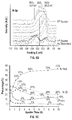
- FIG. 1A illustrates X-ray photoelectron spectroscopy (XPS) data of MoSi x film selectivity on a silicon substrate according to an embodiment described herein.
- XPS X-ray photoelectron spectroscopy
- FIG. 1B illustrate XPS data of MoSi x film selectivity on a silicon oxynitride substrate according to an embodiment described herein.
- FIG. 2A illustrates XPS oxidation state data of Si and Mo on a silicon substrate according to an embodiment described herein.
- FIG. 2B illustrates XPS oxidation state data of Si and Mo on a silicon substrate according to an embodiment described herein.
- FIG. 3A illustrates XPS chemical composition data of various elements present on different substrate types prior to ALD processing according to an embodiment described herein.
- FIG. 3B illustrates XPS chemical composition data of various elements present on different substrate types after 5 ALD cycles according to an embodiment described herein.
- FIG. 3C illustrates XPS chemical composition data of various elements present on different substrate types after additional ALD cycles according to an embodiment described herein.
- FIG. 4A illustrates XPS chemical composition data of various elements present on different substrate types prior to ALD processing according to an embodiment described herein.
- FIG. 4B illustrates XPS chemical composition data of various elements present on different substrate types after 5 ALD cycles according to an embodiment described herein.
- FIG. 4C illustrates XPS chemical composition data of the substrates of FIG. 4B after an annealing process according to an embodiment described herein.
- FIG. 5A illustrates XPS depth profiling data of a MoSi x film after Ar sputtering according to an embodiment described herein.
- FIG. 5B illustrates XPS chemical composition data of the MoSi x film according to an embodiment described herein.
- FIG. 5C illustrates data representative of the chemical composition of the MoSi x film versus time according to an embodiment described herein.
- FIG. 6A illustrates XPS depth profiling data of a MoSi x film after Ar sputtering according to an embodiment described herein.
- FIG. 6B illustrates surface composition data of a MoSi x film according to an embodiment described herein.
- FIG. 6C illustrates bulk composition data of the MoSi x film of FIG. 6B according to an embodiment described herein.
- FIG. 6D illustrates data representative of the chemical composition of the MoSi x film versus time according to an embodiment described herein.
- FIG. 7 is a cross-sectional tunneling electron micrograph (TEM) of a MoSi x film selectively deposited on silicon preferentially to other material present on the substrate according to an embodiment described herein.
- TEM tunneling electron micrograph
- Embodiments described herein include methods which utilize substrate-dependent reactivity of ALD precursors for area-selective deposition. More specifically, embodiments of the disclosure relate to selective deposition of MoSi x on Si preferentially to SiO 2 , SiON and SiN x using substrate selectivity of MoF 6 and Si 2 H 6 . To achieve a stoichiometric MoSi 2 film, additional Si incorporation into the film after the MoF 6 and Si 2 H 6 ALD cycles was performed by dosing Si 2 H 6 onto a Mo rich MoSi x film.
- X-Ray photoelectron spectroscopy revealed that 5 ALD cycles of MoF 6 and Si 2 H 6 selectively deposited a sub-stoichiometric MoSi 2 film on the Si substrate.
- the MoF 6 and Si 2 H 6 precursors were sequentially cycled in a repeating manner with a purge between each successive precursor exposure. Additional Si 2 H 6 doses on the sub-stoichiometric MoSi 2 film incorporated more Si into the film without disturbing the deposition selectivity over SiO 2 and SiN x .
- a bulk of the MoSi x film has a ratio of Si:Mo between about 1.7 and about 1.9 with less than about 10% F and O impurities.
- Embodiments described herein are believed to be advantageous over conventional high pressure Si ALD cycles for the formation of silicide materials, for example, in the formation of source/drain contact structures.
- Deposition selectivity of MoSi x was analyzed, according to the embodiments described herein, on a patterned Si substrate containing three-dimensional (3D) nanoscale SiO 2 and SiN x features.
- Cross-sectional transmission electron microscopy (TEM) indicated that selective MoSi x deposition was achieved on nanoscale 3D structures.
- less than about 10 nuclei/ ⁇ m 2 were present on SiO 2 ; since SiO 2 has approximately A10 7 / ⁇ m 2 OH groups, this corresponds to a selectivity of about 10 7 :1 between the OH groups on SiO 2 and Si—H groups on Si.
- passivant i.e. SAMs
- SiON silicon oxynitride
- Si 3 N 4 Si 3 N 4 , unless otherwise noted, which has been subjected to reactive ion etching and plasma ashing in oxygen during fabrication.
- the SiON substrate contains oxygen which is similar to the conditions of Si 3 N 4 after processing in integrated 3D nanoscale devices.
- the substrates were diced into 12 mm ⁇ 3 mm pieces and degreased with acetone, methanol, and deionized (DI) H 2 O.
- the native oxide on Si was removed by immersing the degreased substrates into a 0.5% HF(aq) solution for 30 seconds.
- the SiO 2 , SiON, and patterned substrates were subjected to the same cleaning procedure.
- a plasma based native oxide removal process may be utilized.
- an NF 3 /H 2 and/or NF 3 NH 3 plasma cleaning process may be utilized to clean and hydrogen terminate a silicon containing surface of the substrates.
- the NF 3 plasma treatment is believed to prevent or substantially reduce deposition selectivity loss by passivating active hydroxyl nucleation sites.
- the native oxide removal process is the SICONI® pre-clean process available from Applied Materials, Inc., Santa Clara, Calif.
- the substrates were blow-dried using high purity N 2 gas.
- the Si, SiO 2 , SiON, and patterned substrate were loaded together on a single substrate holder to expose the substrates to the same ALD conditions.
- the substrates were loaded into a load lock chamber pumped by a turbo molecular pump and backed by a mechanical pump.
- the base pressure of the load lock was about 2.0 ⁇ 10 ⁇ 7 Torr.
- the substrates were transferred in-situ to an ultra-high vacuum chamber with a base pressure of about 3.0 ⁇ 10 ⁇ 10 Torr pumped by an ion pump and titanium sublimation pump.
- the ultra-high vacuum chamber was equipped with a monochromatic XPS apparatus (XM 1000 MkII/SPHERA, available from Scienta Omicron, Inc., Denver, Colo.), a scanning tunneling microscope (STM) (available from Scienta Omicron, Inc., Denver, Colo.), and annealing system using a pyrolytic boron nitride (PBN) heater.
- XM 1000 MkII/SPHERA available from Scienta Omicron, Inc., Denver, Colo.
- STM scanning tunneling microscope
- PBN pyrolytic boron nitride
- the substrates were first annealed at 120° C. in the ultra-high vacuum chamber and the chemical composition of the substrates were determined using XPS.
- the substrates were transferred in-situ to a reaction chamber having a base pressure of about 5.0 ⁇ 10 ⁇ 7 Torr.
- MoSi x deposition MoF 6 (99% purity, available from Synquest Laboratories, Alachua, Fla.) and Si 2 H 6 (99.99% purity, available from Air Liquide USA, LLC, Houston, Tex.) precursors were employed.
- the MoF 6 and Si 2 H 6 doses were regulated using pneumatic valves controlled by LabView software (available from National Instruments, Austin, Tex.).
- An expansion volume was employed for the MoF 6 and Si 2 H 6 doses. Utilization of the expansion volume includes filling a secondary volume with MoF 6 or Si 2 H 6 and dosing the precursors from their respective secondary volumes.
- the fill time for the MoF 6 was between about 10 ms and about 10 ms, such as about 40 ms.
- the dose time for the MoF 6 was between about 10 ms and about 100 ms, such as about 50 ms.
- the fill time for the Si 2 H 6 was between about 1 ms and about 50 ms, such as about 18 ms.
- the dose time for the Si 2 H 6 was between about 1 ms and aboutg 50 ms, such as about 18 ms.
- the pressure spikes during the exposures were monitored using a convectron gauge in the reaction chamber.
- the doses were about 1.8 MegaL for MoF 6 and about 4.2 MegaL for Si 2 H 6 with a 2-minute wait time between the doses.
- the substrates were heated using the PBN heater, and the temperature was maintained at a temperature of between about 100° C. and about 150° C., such as about 120° C.
- the chamber walls were maintained at a temperature of between about 65° C. and about 85° C.
- the MoF 6 doses were between about 1.0 MegaL and about 10 MegaL.
- the Si 2 H 6 doses were between about 1.0 MegaL and about 10 MegaL.
- the substrates were transferred in-situ to the ultra-high vacuum chamber for XPS and STM analysis.
- the X-rays were generated by an Al K ⁇ anode (1486.7 eV).
- XPS data was acquired using constant analyzer-energy (CAE) with a step width of 0.1 eV and a pass energy of 50 eV.
- CAE constant analyzer-energy
- the XPS detector was positioned at 60° to the substrate normal (30° take-off angle from the substrate surface) with a detector-acceptance angle of 7°.
- XPS spectra were analyzed after correcting each peak area with its respective relative sensitivity factor using a Casa XPS v.2.3 program. All of the chemical components in this work were normalized to the sum of all components. Scanning tunnel microscopy was performed with a substrate bias of ⁇ 1.8 V and a constant current of 200 pA.
- Ar + sputtering was performed in conjunction with XPS.
- a lens voltage of 5 kV with a beam current of 1.2 ⁇ A at 6.0 ⁇ 10 ⁇ 7 Torr of Ar was employed; since a raster was used to cover the full substrate area, the current density was approximately 1.2 uA/50 mm 2 .
- the MoSi x substrate was maintained at 25° C. during sputtering to minimize any thermal desorption.
- FIG. 1A illustrates data of the XPS chemical composition of the HF cleaned Si surface before and after sequential doses of MoF 6 and Si 2 H 6 at 120° C.
- Two sets of 5.4 MegaL MoF 6 were dosed on a HF cleaned Si substrate at 120° C.
- XPS showed saturation of Mo at 16%.
- 4.2 Si 2 H 6 MegaL and an additional 42 MegaL of Si 2 H 6 were dosed onto the MoF 6 -saturated Si surface at 120° C. resulting in Si being saturated at 59%.
- the MoF 6 was dosed between about 1 MegaL and about 10 MegaL.
- the SI 2 H 6 was dosed between about 1 MegaL and about 10 MegaL.
- the additional Si 2 H 6 dose was between about 20 MegaL and about 50 MegaL.
- Sequential doses of 4.2 MegaL of Si 2 H 6 and 42 MegaL of Si 2 H 6 indicate that the Si 2 H 6 reaction also saturates on the MoF x covered Si surface. It is believed that with a thicker sub-stoichiometric MoSi 2 film, additional Si can be incorporated onto the surface. However, the Si 2 H 6 reacts in a self-limiting manner on a thinner (monolayer) film of Mo.
- FIG. 1B illustrates XPS chemical composition data for the same series of MoF 6 and Si 2 H 6 saturation doses described above with regard to FIG. 1A but on a SiON substrate. As illustrated, no reaction was observed. It should be noted that while the SiON substrate was nominally SiON, XPS showed only negligible amounts of N on the surface and so this substrate is mostly ion damaged SiO x . After the first 3 pulses of MoF 6 , 8% F and negligible Mo ( ⁇ 1%) were observed. For the rest of the saturation doses, the SiON surface remained unreactive to both MoF 6 and Si 2 H 6 .
- FIGS. 2A and 2B illustrates XPS spectra of Si 2p and Mo 3d for the HF cleaned Si substrate are shown to compare the oxidation states at each experimental operation.
- FIG. 2A illustrates Si 2p peaks after sequential MoF 6 and S 2 H 6 doses show that Si remained in oxidation state of 0 after the 10.8 MegaL of MoF 6 at 120° C. (blue line) which is consistent with Mo—Si bond formation and no etching of Si by F. After the 4.2 MegaL Si 2 H 6 dose at 120° C. (red line), most of the Si stayed in an oxidation state of 0. This is consistent with the formation of a monolayer of MoSi 2 .
- FIG. 2B illustrates Mo 3d peaks after sequential MoF 6 and S 2 H 6 doses shows that the Mo 3d peaks existed in multiple oxidation states after the saturation dose of MoF 6 (black and blue line). After a Si 2 H 6 dose (red line), all of the Mo was reduced and the peak was centered at 227.4 eV which is consistent with MoSi 2 formation.
- FIG. 3A illustrates the chemical composition of a set of three substrates: HF cleaned Si, HF cleaned SiO 2 , and HF cleaned patterned substrate.
- FIG. 3B illustrates the chemical composition of each of the FIG. 3A substrates after 5 ALD cycles of MoF 6 and Si 2 H 6 at 120° C. The data indicated that a Si-deficient MoSi x was selectively deposited on Si and not on SiO 2 . The Si 0 component of the patterned sample was also selectively attenuated by the MoSi x deposition.
- FIG. 3A illustrates the chemical composition of a set of three substrates: HF cleaned Si, HF cleaned SiO 2 , and HF cleaned patterned substrate.
- FIG. 3B illustrates the chemical composition of each of the FIG. 3A substrates after 5 ALD cycles of MoF 6 and Si 2 H 6 at 120° C. The data indicated that a Si-deficient MoSi x was selectively deposited on Si and not on SiO 2 . The Si 0 component of
- 3C illustrates the chemical composition of each of the FIG. 3B substrates after an additional 25.2 MegaL (between 3 pulses and 10 pulses) of Si 2 H 6 .
- the additional Si 2 H 6 incorporated Si onto the MoSi x surface. Selectivity with respect to SiO 2 was maintained during the additional Si 2 H 6 pulses (SiO 2 had 0% Mo and 0% Si 0 throughout the ALD process).
- the three substrates were loaded together on a single substrate holder to ensure that they were exposed to identical deposition conditions.
- the Si and SiO 2 substrates allowed verification of selectivity during deposition on the patterned substrate.
- the patterned substrate has SiO 2 layers sandwiched by SiN x on top of the Si substrate. It is noted that the SiN x on the patterned substrate was actually SiON since it was ion damaged and ashed in O 2 during fabrication.
- a 30 s HF clean removed the native oxide on Si.
- the thermally grown SiO 2 was 300 nm thick and the 30 s of HF clean did not change the elemental composition or oxidation states of SiO 2 .
- the HF cleaned patterned substrate was composed of a mixture of SiN x , SiO x and Si 0 .
- XPS was performed after 5 ALD cycles of MoF 6 and Si 2 H 6 at 120° C. as shown in FIG. 3B .
- XPS showed a surface composition of 32% Mo and 10% Si on the Si substrate which corresponds to highly Si-deficient MoSi x .
- MoSi x deposition on the SiO 2 substrate consistent with highly selective ALD.
- XPS showed that 5% Mo was deposited, and the Si 0 was attenuated to 1%.
- the fraction of N and O at the surface did not change significantly during ALD on the patterned substrate.
- the data is consistent with Si-deficient MoSi x being deposited selectivity on the 6% of Si 0 on the patterned substrate.
- Deposition selectivity on the pattern substrates is consistent with three aspects of embodiments described herein: (1) MoSi x deposition on the Si substrate but not on the SiO 2 substrate. (2) After the MoSi x deposition, the Si 0 (not the higher oxidation state Si peaks from Si—N and Si—O) was attenuated on the pattered substrate. (3) Numerically, about 4% Mo deposition on the patterned substrate with 6% Si 0 is proportional to having 32% Mo on the Si substrate with 54% Si 0 on the HF clean surface.
- the three substrates were exposed to an additional 25.2 MegaL (between 3 pulses and 10 pulses, such as 6 pulses) of Si 2 H 6 at 120° C. (See FIG. 3C ).
- Si 2 H 6 increased to 20% on the Si substrate consistent with Si being incorporated into the film or on the surface of the substrate.
- the additional Si 2 H 6 doses did not decrease the selectivity for deposition on Si versus SiO 2 .
- FIGS. 4A-4C illustrate XPS chemical composition data of selective MoSi x deposition on HF cleaned Si, SiO 2 , and SiON with a post deposition anneal.
- FIG. 4A illustrates XPS chemical composition of Si, SiO 2 , and SiON substrates after the HF clean.
- FIG. 4B illustrates XPS chemical composition data showing the MoSi x was selectively deposited only on Si after the 5 ALD cycles of MoSi x followed by the additional 6 pulses (25.2 MegaL) of Si 2 H 6 at 120° C.
- FIG. 4C illustrates XPS chemical composition data of the substrates with a post-deposition anneal (PDA) performed at 520° C. for 3 mins. As illustrated, the PDA removed F from the MoSi x film and reduced the Mo to Mo 0 .
- PDA post-deposition anneal
- FIG. 4A illustrates that the SiON surface is composed primarily of SiN x after the HF clean.
- the three substrates were annealed at 520° C. for 3 minutes which decreased F from 25% to 3% on the Si substrate.
- the 520° C. PDA also reduced the Mo to Mo 0 on the Si substrate and decreased the Si:Mo ratio from about 0.75 to about 0.5 at the surface. This is consistent with the desorption of surface F in the form of SiHF 3 or SiF 4 .
- the XPS analysis of the PDA indicates that the F is removed from the film by the PDA which reduces the probability of F diffusion into adjacent MOSFET device structures.
- Ex-situ AFM image data of the SiO 2 substrate surface after dosing 5 ALD cycles at 120° C. followed by an in-situ 550° C. anneal for 3 minutes in order to confirm the selectivity was performed by counting the number of nuclei on the substrate surface.
- the density of nuclei was about 9 nuclei/ ⁇ m 2 which confirms the Si deposition preference over SiO 2 . It is believed that the high deposition selectivity of the embodiments described herein is further improved by controlling wall temperature of the reaction chamber and by using short high pressure Si 2 H 6 pulses and longer purge cycles to facilitate ALD and avoid a CVD deposition regime.
- FIG. 5A illustrates XPS chemical composition data after Ar + sputtering on HF cleaned Si after the 5 cycles of MoF 6 and Si 2 H 6 at 120° C.
- FIG. 5B illustrates XPS peaks of Si 2p after sequential Ar + sputtering, the results of which show that the bulk of the MoSi x film consisted mostly of Si 0 .
- FIG. 5C illustrates chemical composition data of the deposited film plotted versus Ar + sputter time on Si after 5 cycles of MoF 6 and Si 2 H 6 at 120° C.
- the XPS data shown in FIG. 5A was derived from the MoSi x film deposited on a HF cleaned Si substrate at 120° C. using 5 ALD cycles of MoF 6 and Si 2 H 6 without additional Si 2 H 6 incorporation. As the sputtering time increased, the MoSi x film became thinner until the underlying Si substrate was exposed. The first 10 mins of sputtering decreased the F from 35% to 8% while the Mo shifted from a mixture of oxidized Mo and Mo 0 to pure Mo 0 . The data is consistent with the surface F being bonded primarily to Mo.
- the Si 0 to Mo 0 ratio was employed to distinguish the pure MoSi x phase because, in the pure MoSi x phase, both Mo and Si are bonded to each other and have an oxidation state of 0. After removal of the silicon oxide and MoF x species at the substrate surface, the percentage of Si 0 exceeded that of Mo 0 .
- the Si 0 :Mo 0 ratio in the bulk of the MoSi x film was 1.41 which corresponds to a Si-deficient MoSi x film. It is noted that in the center of the film the Si:Mo ratio is 1.77 therefore, in the absence of background O 2 /H 2 O, it is possible the Si 0 :Mo 0 ratio would be closer to 2.
- FIG. 5B illustrates the raw XPS spectra of Si 2p corresponding to each XPS measurement of FIG. 5A .
- the Si peak at 99.2 eV increased and broadened to higher binding energy after the 4 th sputtering cycle.
- the energy of the Mo peak corresponded to Mo 0 after each sputtering cycle.
- the bulk MoSi x film is predominantly Si 0 and Mo 0 in the form of MoSi x while the top surface and the bottom interface was rich in SiO x .
- the top SiO x is consistent with contamination from the chamber environment while the bottom interfacial oxide is consistent with the imperfect ex-situ HF clean.
- FIG. 5C illustrates the percentages of the chemical components obtained from the XPS measurement in FIG. 5A .
- F decreased to below 3% and eventually reached 0%.
- O in the bulk of the film was ⁇ 10% but slowly increased to 15% at the MoSi x —Si interface which is consistent with the existence of an interfacial oxide layer.
- FIGS. 6A-6D illustrate XPS profile data of the MoSi x film with after exposure to the additional Si 2 H 6 doses.
- FIG. 6A illustrates XPS chemical composition data after Ar + sputtering dry cleaned Si after 5 cycles of MoF 6 and Si 2 H 6 followed by additional 6 pulses (25.2 MegaL) of Si 2 H 6 at 120° C.
- FIG. 6B illustrates XPS surface composition data after 5 ALD cycles of MoF 6 and Si 2 H 6 with and without extra Si 2 H 6 pulses. Si:Mo ratios were 0.33 for 5 ALD and 0.89 for 5ALD+6 ⁇ Si 2 H 6 which is consistent with Si incorporation on the surface.
- FIG. 6A illustrates XPS chemical composition data after Ar + sputtering dry cleaned Si after 5 cycles of MoF 6 and Si 2 H 6 followed by additional 6 pulses (25.2 MegaL) of Si 2 H 6 at 120° C.
- FIG. 6B illustrates XPS surface composition data after 5 ALD cycles of MoF 6 and Si 2
- FIG. 6C illustrates XPS bulk composition data of MoSi x with and without extra Si 2 H 6 pulses after removing surface contaminations using the Ar + sputtering. Si:Mo ratios were 1.77 for 5 ALD and 1.96 for 5ALD+6 ⁇ Si 2 H 6 .
- FIG. 6D illustrates XPS chemical composition data of the MoSi x film is plotted versus Ar + sputter time on Si after 5 cycles of MoF 6 and Si 2 H 6 followed by additional Si 2 H 6 pulses at 120° C.
- FIG. 6A presents a series of depth-profile XPS after each operation performed on the dry cleaned substrate.
- F was mostly removed after the 530° C. anneal and the Mo was all reduced to Mo 0 which was consistent with the desorption of F from the surface as presented in FIG. 4C .
- the Si:Mo ratio was 0.89 at this operation.
- the Si:Mo ratio of the MoSi x film without the extra Si 2 H 6 doses was only 0.33 as illustrated in FIG. 6B .
- FIG. 6D shows the XPS percentage of each chemical component in the function of the Ar + sputter time which is consistent with the MoSi x formation in bulk of the MoSi x film.
- 4.2 MegaL of Si 2 H 6 was introduced to the reaction chamber over a duration of 6 seconds using a pneumatic valve.
- the Si 2 H 6 process characteristics utilize an approximately 3 times larger Si 2 H 6 exposure over a dosing duration about 10 times shorter than conventional Si 2 H 6 dosing parameters.
- embodiments described herein utilize a 30 ⁇ higher partial pressure during the ALD dose when compared to conventional dosing regimes.
- the 30 ⁇ higher instantaneous pressure during dosing is believed to enable a precursor mediated Si 2 H 6 chemisorption layer to remain on the surface long enough to react with the Mo to incorporate more Si into the MoSi x film.
- the Si incorporation is also believed to be self-limiting which enables a growth rate of MoSi x of about 1.2 nm/cycle.
- the resistance of the MoSi x film was measured using a 4-point probe measurement.
- updoped Si (001) with >10000 ohm ⁇ cm resistance was used as a substrate.
- 10 cycles of MoSi x ALD at 120° C. was deposited on an HF cleaned intrinsic (semi-insulating) Si substrate followed by an in-situ 550° C. anneal for 3 minutes and a 900° C. spike anneal in 5% H 2 balanced in N 2 .
- Ni dots were deposited as a probe contact.
- FIG. 7 is a cross-sectional TEM image of the MoSi x /HF cleaned patterned substrate.
- MoSi x ALD 5 cycles of MoSi x ALD followed by an additional 25.2 MegaL of Si 2 H 6 were dosed at 120° C.
- the elemental composition of this substrate at each deposition step is shown in FIGS. 3A-3C .
- the TEM image shows complete selectivity of MoSi x deposition on Si but not on SiN x nor SiO 2 .
- the thickness of the MoSi x film deposited on Si was about 6.3 nm after the 5 ALD cycles followed by an additional 25.2 MegaL which achieved a growth rate of about 1.2 nm/cycle. Due to the growth rate per cycle of MoSi x ALD, 5 ALD cycles is believed to be sufficient for contact materials and contact device structures.
- Selective atomic layer deposition of sub-stoichiometric MoSi 2 was achieved by a selective process on hydrogen-terminated Si versus thermally grown SiO 2 , ion damaged SiON, and SiN x .
- the selectivity is based on the favorable reactivity of MoF 6 and Si 2 H 6 on H—Si but not on SiO 2 or SiN x since Si—O, Si—N, and SiO—H bonds are strong enough that they cannot be cleaved by either precursor at 120° C.
- Both MoF 6 and Si 2 H 6 showed self-limiting behavior which allowed deposition of a highly conformal and smooth film with a root mean square (RMS) roughness of 2.8 ⁇ .
- RMS root mean square
- the surface of the MoSi x film after 5 ALD cycles showed a highly Si-deficient MoSi x surface with Si:Mo ratio of 0.33 and this Si:Mo ratio at the surface is improved to 0.89 by pulsing extra Si 2 H 6 .
- the cross-sectional TEM imaging shows that the selectivity is retained on the nanoscale and that MoSi x can be selectively deposited on Si without substrate consumption.
- the MoSi x film growth rate of about 1.2 nm/cycle enables less than 10 ALD cycles, such as 5 ALD cycles, to be sufficient for utilization of the MoSi x film as a contact material. Accordingly, process throughput is increased by utilizing the embodiments described herein when compared to conventional ALD processes. It is believed the selective MoSi x deposition eliminates or substantially reduces reliance on lithography processes for complicated 3D MOSFET structures (e.g FinFETs). The selectivity for Si—H bonds vs SiO—H bonds exceeds 10 6 . Thus, high selectivity is possible on the nanoscale even without the use additional passivation layers. The embodiments described herein also illustrate that ALD of silicide versus metal could readily be switched while retaining selectivity by changing the partial pressure during the ALD pulse of the reductant.
Landscapes
- Engineering & Computer Science (AREA)
- Physics & Mathematics (AREA)
- Condensed Matter Physics & Semiconductors (AREA)
- General Physics & Mathematics (AREA)
- Manufacturing & Machinery (AREA)
- Computer Hardware Design (AREA)
- Microelectronics & Electronic Packaging (AREA)
- Power Engineering (AREA)
- Chemical & Material Sciences (AREA)
- Chemical Kinetics & Catalysis (AREA)
- General Chemical & Material Sciences (AREA)
- Electrodes Of Semiconductors (AREA)
- Insulated Gate Type Field-Effect Transistor (AREA)
- Chemical Vapour Deposition (AREA)
- Physical Vapour Deposition (AREA)
- Formation Of Insulating Films (AREA)
Abstract
Description
MoF6(g)+1.55i2H6(g)→MoSi2(s)+SiF4(g)+3.5H2(g)+2HF(g)
MoF6(g)+Si2H6(g)→Mo(s)+2SiHF3(g)+2H2(g) 1:
2MoF6(g)+1.5Si2H6(g)→2Mo(s)+2SiF4(g)SiHF3(g)+3.5H2(g)+2HF(g) 2:
ρ=ktR max=(4.53)×(10×10−7)×(110)=498 μΩcm
where k is a constant, t is thickness and Rmax is the measured maximum resistance.
Claims (18)
Priority Applications (2)
| Application Number | Priority Date | Filing Date | Title |
|---|---|---|---|
| US15/988,820 US10475655B2 (en) | 2017-05-26 | 2018-05-24 | Selective deposition of metal silicides |
| US16/189,429 US10586707B2 (en) | 2017-05-26 | 2018-11-13 | Selective deposition of metal silicides |
Applications Claiming Priority (2)
| Application Number | Priority Date | Filing Date | Title |
|---|---|---|---|
| US201762511521P | 2017-05-26 | 2017-05-26 | |
| US15/988,820 US10475655B2 (en) | 2017-05-26 | 2018-05-24 | Selective deposition of metal silicides |
Related Child Applications (1)
| Application Number | Title | Priority Date | Filing Date |
|---|---|---|---|
| US16/189,429 Continuation-In-Part US10586707B2 (en) | 2017-05-26 | 2018-11-13 | Selective deposition of metal silicides |
Publications (2)
| Publication Number | Publication Date |
|---|---|
| US20180342395A1 US20180342395A1 (en) | 2018-11-29 |
| US10475655B2 true US10475655B2 (en) | 2019-11-12 |
Family
ID=64397046
Family Applications (1)
| Application Number | Title | Priority Date | Filing Date |
|---|---|---|---|
| US15/988,820 Active US10475655B2 (en) | 2017-05-26 | 2018-05-24 | Selective deposition of metal silicides |
Country Status (5)
| Country | Link |
|---|---|
| US (1) | US10475655B2 (en) |
| JP (1) | JP6989623B2 (en) |
| KR (2) | KR102455480B1 (en) |
| CN (1) | CN110945626B (en) |
| WO (1) | WO2018218078A1 (en) |
Cited By (1)
| Publication number | Priority date | Publication date | Assignee | Title |
|---|---|---|---|---|
| US11380536B2 (en) | 2020-05-05 | 2022-07-05 | Applied Materials, Inc. | Multi-step pre-clean for selective metal gap fill |
Families Citing this family (2)
| Publication number | Priority date | Publication date | Assignee | Title |
|---|---|---|---|---|
| KR20230139306A (en) | 2022-03-25 | 2023-10-05 | 에스케이스페셜티 주식회사 | Substrate Processing Method and Selective Deposition Method using the Same |
| KR20240053803A (en) | 2022-10-18 | 2024-04-25 | 에스케이스페셜티 주식회사 | Substrate processing method and area selective thin film deposition method using the substrate processing method |
Citations (6)
| Publication number | Priority date | Publication date | Assignee | Title |
|---|---|---|---|---|
| US20040102033A1 (en) | 2002-11-21 | 2004-05-27 | Texas Instruments, Incorporated | Method for forming a ternary diffusion barrier layer |
| US20060210723A1 (en) | 2005-03-21 | 2006-09-21 | Tokyo Electron Limited | Plasma enhanced atomic layer deposition system and method |
| US7135418B1 (en) | 2005-03-09 | 2006-11-14 | Novellus Systems, Inc. | Optimal operation of conformal silica deposition reactors |
| US20130189837A1 (en) | 2010-06-10 | 2013-07-25 | Asm International N.V. | Selective formation of metallic films on metallic surfaces |
| US9034773B2 (en) | 2012-07-02 | 2015-05-19 | Novellus Systems, Inc. | Removal of native oxide with high selectivity |
| US20170037513A1 (en) | 2015-08-03 | 2017-02-09 | Asm Ip Holding B.V. | Selective deposition on metal or metallic surfaces relative to dielectric surfaces |
Family Cites Families (10)
| Publication number | Priority date | Publication date | Assignee | Title |
|---|---|---|---|---|
| JPS61128521A (en) * | 1984-11-27 | 1986-06-16 | Nippon Telegr & Teleph Corp <Ntt> | Manufacture of semiconductor device |
| JPH0666286B2 (en) * | 1987-08-24 | 1994-08-24 | 富士通株式会社 | Method for forming silicon-containing metal film |
| JPH05144710A (en) * | 1991-11-22 | 1993-06-11 | Hitachi Ltd | Optical element and fabrication thereof |
| JPH07283168A (en) * | 1994-04-15 | 1995-10-27 | Mitsubishi Electric Corp | Semiconductor device and manufacture thereof |
| US7780793B2 (en) * | 2004-02-26 | 2010-08-24 | Applied Materials, Inc. | Passivation layer formation by plasma clean process to reduce native oxide growth |
| TW200746268A (en) * | 2006-04-11 | 2007-12-16 | Applied Materials Inc | Process for forming cobalt-containing materials |
| US8808563B2 (en) * | 2011-10-07 | 2014-08-19 | Applied Materials, Inc. | Selective etch of silicon by way of metastable hydrogen termination |
| US20160042968A1 (en) * | 2014-08-05 | 2016-02-11 | Applied Materials, Inc. | Integrated oxide and si etch for 3d cell channel mobility improvements |
| US20170029948A1 (en) * | 2015-07-28 | 2017-02-02 | Asm Ip Holding B.V. | Methods and apparatuses for temperature-indexed thin film deposition |
| WO2017056187A1 (en) * | 2015-09-29 | 2017-04-06 | 株式会社日立国際電気 | Semiconductor device manufacturing method, substrate processing device, and recording medium |
-
2018
- 2018-05-24 WO PCT/US2018/034482 patent/WO2018218078A1/en active Application Filing
- 2018-05-24 US US15/988,820 patent/US10475655B2/en active Active
- 2018-05-24 KR KR1020217038234A patent/KR102455480B1/en active IP Right Grant
- 2018-05-24 JP JP2019565324A patent/JP6989623B2/en active Active
- 2018-05-24 CN CN201880034866.0A patent/CN110945626B/en active Active
- 2018-05-24 KR KR1020197037816A patent/KR20200000457A/en active Application Filing
Patent Citations (6)
| Publication number | Priority date | Publication date | Assignee | Title |
|---|---|---|---|---|
| US20040102033A1 (en) | 2002-11-21 | 2004-05-27 | Texas Instruments, Incorporated | Method for forming a ternary diffusion barrier layer |
| US7135418B1 (en) | 2005-03-09 | 2006-11-14 | Novellus Systems, Inc. | Optimal operation of conformal silica deposition reactors |
| US20060210723A1 (en) | 2005-03-21 | 2006-09-21 | Tokyo Electron Limited | Plasma enhanced atomic layer deposition system and method |
| US20130189837A1 (en) | 2010-06-10 | 2013-07-25 | Asm International N.V. | Selective formation of metallic films on metallic surfaces |
| US9034773B2 (en) | 2012-07-02 | 2015-05-19 | Novellus Systems, Inc. | Removal of native oxide with high selectivity |
| US20170037513A1 (en) | 2015-08-03 | 2017-02-09 | Asm Ip Holding B.V. | Selective deposition on metal or metallic surfaces relative to dielectric surfaces |
Non-Patent Citations (32)
| Title |
|---|
| A. H. Reader, et al, Transition Metal Silicides in Silicon Technology, Rep. Prog. Phys., 1992, 56, 72 pp. |
| Alfredo Mameli, et al., Area-Selective Atomic Layer Deposition of SiO2 Using Acetylacetone as a Chemoselective Inhibitor in an ABC-Type Cycle, ACS Nano 2017, 11, 9 pp. |
| Berc Kalanyan, et al, Using Hydrogen To Expand the Inherent Substrate Selectivity Window During Tungsten Atomic Layer Deposition, Chemistry of Materials, 2016, 28, 10 pp. |
| C.-H. Jan, et al., A 22nm SoC Platform Technology Featuring 3-D Tri-Gate and High-k/Metal Gate, Optimized for Ultra Low Power, High Performance and High Density SoC Applications, 2012 International Electron Devices Meeting, 4 pp. |
| D. Kirillov, et al, Raman Scattering Study of Plasma Etching Damage in GaAs, Journal of Vacuum Science & Technology B: Microelectronics Processing and Phenomena 1986, 4, 3 pp. |
| D. Seghete, et al, Molybdenum Atomic Layer Deposition Using MoF6 and Si2H6 as the Reactants, Chem. Mater. 2011, 23, 11 pp. |
| Der-Gao Lin, et al, The Effect of Fluorine on MOSFET Channel Length, IEEE Electron Device Letters, Oct. 10, 1993, 14 (10), 3 pp. |
| Deuk-Sung Choi, Fluorine Effects on NMOS Characteristics and DRAM Refresh, Journal of Semiconductor Technology and Science, Mar. 2012, 12 (1), 5 pp. |
| E. K. Broadbent, et al, Selective Low Pressure Chemical Vapor Deposition of Tungsten, J. Electrochem. Soc. 1984 131 (6), 7 pp. |
| Fatemeh Sadat Minaye Hashemi, et al., Self-Correcting Process for High Quality Patterning by Atomic Layer Deposition, ACS Nano, 2015, 9 (9) 8 pp. |
| International Search Report and Written Opinion dated Aug. 24, 2018 for Application No. PCT/US2018/034482. |
| J. Alexander Liddle, et al., Nanomanufacturing: A Perspective, ACS Nano, 2016, 10 (3), 84 pp. |
| J.W. Klaus, et al, Atomic Layer Deposition of Tungsten Using Sequential Surface Chemistry; with a Sacrificial Stripping Reaction, Thin Solid Films, 2000, 360, 9 pp. |
| Jin Xie, et al., Site-Selective Deposition of Twinned Platinum Nanoparticles on TiSi2 Nanonets by Atomic Layer Deposition and Their Oxygen Reduction Activities, 2013, 7 (7), 9 pp. |
| Jinhee Kwon, et al, Substrate Selectivity of (tBu-Allyl)Co(CO)3 during Thermal Atomic Layer Deposition of Cobalt, Chem. Mater. 2012, 24, 6 pp. |
| Karla Bernal-Ramos, et al, Atomic Layer Deposition of Cobalt Silicide Thin Films Studied by in Situ Infrared Spectroscopy, Chem. Mater. 2015, 27, 7 pp. |
| Kow Ming Chang, et al, Reduction of Selectivity Loss Probability on Dielectric Surface during Chemical Vapor Deposition of Tungsten Using Fluorinated Oxide and Removing Silanol Units on Dielectric Surface, Jpn. Appl. Phys., 1996, 35, 8 pp. |
| Kyungtae Lee, et al., Selective positioning of organic dyes in a; mesoporous inorganic oxide film, Nature Materials, 2009, 8, 8 pp. |
| M. A. Chesters, J. Phys. Condens. Matter, 3, S251 (1991). |
| M. Y. Tsai, et al, One?Micron Polycide (WSi2 on Poly?Si) MOSFET Technology, J. Electrochem. Soc. 1981, 128 (10), 8 pp. |
| Marissa M. Kerrigan, et al, Substrate Selectivity in the Low Temperature Atomic Layer Deposition of Cobalt Metal Films from Bis(1,4-di-tert-butyl-1,3-diazadienyl)cobalt and Formic acid, The Journal of Chemical Physics 2017, 146, 9 pp. |
| Mi H. Park, et al., Selective Atomic Layer Deposition of Titanium Oxide on Patterned Self-Assembled Monolayers Formed by Microcontact Printing. Langmuir, 2004, 20 (6), 4 pp. |
| Ming Fang, et al., Area-Selective Atomic Layer Deposition: Conformal Coating, Subnanometer Thickness Control, and Smart Positioning, ACS Nano, 2015, 9 (9), 4 pp. |
| Paul C. Lemaire, et al, Understanding Inherent Substrate Selectivity During Atomic Layer Deposition: Effect of Surface Preparation, Hydroxyl Density, and Metal Oxide Composition on Nucleation Mechanisms During Tungsten ALD, The Journal of Chemical Physics, 2017 146, 10 pp. |
| Ph. Gouy-Pailler, et al, Selective Deposition of Tungsten by Chemical Vapour Deposition from SiH4 Reduction of WF6, Thin Solid Films, 1994, 241, 4 pp. |
| Roger Mueller, et al, OH Surface Density of SiO2 and TiO2 by Thermogravimetric Analysis, Langmuir 2003, 19, 6 pp. |
| S. P. Murarka, Transition Metal Silicides, Ann. Rev. Mater. Sci., 1983, 13, 22 pp. |
| Sarah E. Atanasov, et al, Inherent Substrate-dependent Growth Initiation and Selective-area Atomic Layer Deposition of TiO2 Using "Water-free" Metal-halide/metal Alkoxide Reactants, Journal of Vacuum Science and Technology A, Jan./Feb. 2016, 34 (1), 10 pp. |
| Thomas Proslier, et al, Atomic Layer Deposition and Superconducting Properties of NbSi Films, J. Phys. Chem. C, 2011, 115 (19), 26 pp. |
| Woo-Hee Kim, et al., A Process for Topographically-Selective Deposition on 3D Nanostructures by Ion Implantation, ACS Nano, Mar. 7, 2016, 22 pp. |
| Y. J. Chabel, et al, Infrared Spectroscopy of Si(111) and Si(100) Surfaces After HF Treatment: Hydrogen Termination and Surface Morphology, J. Vac. Sci. Tehnology May/Jun. 1989, 7 (3), 6 pp. |
| Yuichiro Mitani, et al, Improvement of Charge-to-Breakdown Distribution by Fluorine Incorporation Into Thin Gate Oxides, IEEE Transactions on Electron Devices, Nov. 2003, 50 (11), 6 pp. |
Cited By (2)
| Publication number | Priority date | Publication date | Assignee | Title |
|---|---|---|---|---|
| US11380536B2 (en) | 2020-05-05 | 2022-07-05 | Applied Materials, Inc. | Multi-step pre-clean for selective metal gap fill |
| US11776806B2 (en) | 2020-05-05 | 2023-10-03 | Applied Materials, Inc. | Multi-step pre-clean for selective metal gap fill |
Also Published As
| Publication number | Publication date |
|---|---|
| WO2018218078A1 (en) | 2018-11-29 |
| KR102455480B1 (en) | 2022-10-18 |
| CN110945626A (en) | 2020-03-31 |
| US20180342395A1 (en) | 2018-11-29 |
| JP6989623B2 (en) | 2022-01-05 |
| JP2020522138A (en) | 2020-07-27 |
| KR20210144949A (en) | 2021-11-30 |
| CN110945626B (en) | 2023-07-04 |
| KR20200000457A (en) | 2020-01-02 |
Similar Documents
| Publication | Publication Date | Title |
|---|---|---|
| TWI804706B (en) | Method of topology-selective film formation of silicon oxide | |
| KR100871006B1 (en) | Thin tungsten silicide layer deposition and gate metal integration | |
| US10475655B2 (en) | Selective deposition of metal silicides | |
| US10483097B2 (en) | Method for cleaning, passivation and functionalization of Si—Ge semiconductor surfaces | |
| Choi et al. | Selective atomic layer deposition of MoSix on Si (0 0 1) in preference to silicon nitride and silicon oxide | |
| US10373824B2 (en) | CVD silicon monolayer formation method and gate oxide ALD formation on semiconductor materials | |
| Milojevic et al. | Characterization of the “clean-up” of the oxidized Ge (100) surface by atomic layer deposition | |
| US20180308685A1 (en) | Low temperature selective epitaxial silicon deposition | |
| US20170040159A1 (en) | Self-limiting and saturating chemical vapor deposition of a silicon bilayer and ald | |
| EP3881349A1 (en) | Selective deposition of metal silicides and selective oxide removal | |
| US10262858B2 (en) | Surface functionalization and passivation with a control layer | |
| US10586707B2 (en) | Selective deposition of metal silicides | |
| US20170040158A1 (en) | Low temperature ald on semiconductor and metallic surfaces | |
| TWI780157B (en) | Selective deposition of metal silicides | |
| TWI833831B (en) | Selective deposition of metal silicides and selective oxide removal | |
| US11367614B2 (en) | Surface roughness for flowable CVD film | |
| US20220375747A1 (en) | Flowable CVD Film Defect Reduction | |
| TWI740933B (en) | Surface functionalization and passivation with a control layer | |
| Choi | Area-selective Atomic Layer Deposition of Silicide and Oxides Using Inherent Substrate Dependent Processes |
Legal Events
| Date | Code | Title | Description |
|---|---|---|---|
| FEPP | Fee payment procedure |
Free format text: ENTITY STATUS SET TO UNDISCOUNTED (ORIGINAL EVENT CODE: BIG.); ENTITY STATUS OF PATENT OWNER: LARGE ENTITY |
|
| AS | Assignment |
Owner name: APPLIED MATERIALS, INC., CALIFORNIA Free format text: ASSIGNMENT OF ASSIGNORS INTEREST;ASSIGNORS:HUNG, RAYMOND HOIMAN;KIM, NAMSUNG;NEMANI, SRINIVAS;AND OTHERS;SIGNING DATES FROM 20180606 TO 20180806;REEL/FRAME:046700/0416 |
|
| STPP | Information on status: patent application and granting procedure in general |
Free format text: NON FINAL ACTION MAILED |
|
| STPP | Information on status: patent application and granting procedure in general |
Free format text: RESPONSE TO NON-FINAL OFFICE ACTION ENTERED AND FORWARDED TO EXAMINER |
|
| STPP | Information on status: patent application and granting procedure in general |
Free format text: NOTICE OF ALLOWANCE MAILED -- APPLICATION RECEIVED IN OFFICE OF PUBLICATIONS |
|
| AS | Assignment |
Owner name: THE REGENTS OF THE UNIVERSITY OF CALIFORNIA, CALIF Free format text: ASSIGNMENT OF ASSIGNORS INTEREST;ASSIGNORS:CHOI, JONG;AHLES, CHRISTOPHER;KUMMEL, ANDREW;SIGNING DATES FROM 20190711 TO 20190812;REEL/FRAME:050266/0456 |
|
| STPP | Information on status: patent application and granting procedure in general |
Free format text: PUBLICATIONS -- ISSUE FEE PAYMENT VERIFIED |
|
| STCF | Information on status: patent grant |
Free format text: PATENTED CASE |
|
| MAFP | Maintenance fee payment |
Free format text: PAYMENT OF MAINTENANCE FEE, 4TH YEAR, LARGE ENTITY (ORIGINAL EVENT CODE: M1551); ENTITY STATUS OF PATENT OWNER: LARGE ENTITY Year of fee payment: 4 |