US10438795B2 - Self-centering wafer carrier system for chemical vapor deposition - Google Patents
Self-centering wafer carrier system for chemical vapor deposition Download PDFInfo
- Publication number
- US10438795B2 US10438795B2 US15/178,723 US201615178723A US10438795B2 US 10438795 B2 US10438795 B2 US 10438795B2 US 201615178723 A US201615178723 A US 201615178723A US 10438795 B2 US10438795 B2 US 10438795B2
- Authority
- US
- United States
- Prior art keywords
- wafer carrier
- wafer
- self
- centering
- rotating tube
- Prior art date
- Legal status (The legal status is an assumption and is not a legal conclusion. Google has not performed a legal analysis and makes no representation as to the accuracy of the status listed.)
- Active, expires
Links
- 238000005229 chemical vapour deposition Methods 0.000 title claims abstract description 83
- 238000000034 method Methods 0.000 claims abstract description 60
- 238000012545 processing Methods 0.000 claims abstract description 24
- 239000000758 substrate Substances 0.000 claims description 44
- 239000000463 material Substances 0.000 claims description 29
- 125000006850 spacer group Chemical group 0.000 claims description 26
- 239000010453 quartz Substances 0.000 claims description 23
- HBMJWWWQQXIZIP-UHFFFAOYSA-N silicon carbide Chemical compound [Si+]#[C-] HBMJWWWQQXIZIP-UHFFFAOYSA-N 0.000 claims description 23
- VYPSYNLAJGMNEJ-UHFFFAOYSA-N silicon dioxide Inorganic materials O=[Si]=O VYPSYNLAJGMNEJ-UHFFFAOYSA-N 0.000 claims description 23
- 230000003068 static effect Effects 0.000 claims description 21
- 238000010438 heat treatment Methods 0.000 claims description 18
- 229910010271 silicon carbide Inorganic materials 0.000 claims description 17
- 238000010926 purge Methods 0.000 claims description 15
- OKTJSMMVPCPJKN-UHFFFAOYSA-N Carbon Chemical compound [C] OKTJSMMVPCPJKN-UHFFFAOYSA-N 0.000 claims description 10
- 229910002804 graphite Inorganic materials 0.000 claims description 9
- 239000010439 graphite Substances 0.000 claims description 9
- 239000003870 refractory metal Substances 0.000 claims description 8
- 229910052580 B4C Inorganic materials 0.000 claims description 4
- PNEYBMLMFCGWSK-UHFFFAOYSA-N aluminium oxide Inorganic materials [O-2].[O-2].[O-2].[Al+3].[Al+3] PNEYBMLMFCGWSK-UHFFFAOYSA-N 0.000 claims description 4
- INAHAJYZKVIDIZ-UHFFFAOYSA-N boron carbide Chemical compound B12B3B4C32B41 INAHAJYZKVIDIZ-UHFFFAOYSA-N 0.000 claims description 4
- 239000011248 coating agent Substances 0.000 claims description 4
- 238000000576 coating method Methods 0.000 claims description 4
- JBRZTFJDHDCESZ-UHFFFAOYSA-N AsGa Chemical compound [As]#[Ga] JBRZTFJDHDCESZ-UHFFFAOYSA-N 0.000 claims description 3
- 229910002601 GaN Inorganic materials 0.000 claims description 3
- 229910001218 Gallium arsenide Inorganic materials 0.000 claims description 3
- 229910010293 ceramic material Inorganic materials 0.000 claims description 3
- 229910052594 sapphire Inorganic materials 0.000 claims description 3
- 239000010980 sapphire Substances 0.000 claims description 3
- PIGFYZPCRLYGLF-UHFFFAOYSA-N Aluminum nitride Chemical compound [Al]#N PIGFYZPCRLYGLF-UHFFFAOYSA-N 0.000 claims description 2
- PZNSFCLAULLKQX-UHFFFAOYSA-N Boron nitride Chemical compound N#B PZNSFCLAULLKQX-UHFFFAOYSA-N 0.000 claims description 2
- JMASRVWKEDWRBT-UHFFFAOYSA-N Gallium nitride Chemical compound [Ga]#N JMASRVWKEDWRBT-UHFFFAOYSA-N 0.000 claims description 2
- XUIMIQQOPSSXEZ-UHFFFAOYSA-N Silicon Chemical compound [Si] XUIMIQQOPSSXEZ-UHFFFAOYSA-N 0.000 claims description 2
- 238000013459 approach Methods 0.000 claims description 2
- 229910052593 corundum Inorganic materials 0.000 claims description 2
- 229910052710 silicon Inorganic materials 0.000 claims description 2
- 239000010703 silicon Substances 0.000 claims description 2
- 229910001845 yogo sapphire Inorganic materials 0.000 claims description 2
- 235000012431 wafers Nutrition 0.000 description 418
- 238000013461 design Methods 0.000 description 16
- 239000007789 gas Substances 0.000 description 16
- 238000000151 deposition Methods 0.000 description 14
- 239000000969 carrier Substances 0.000 description 12
- 239000004065 semiconductor Substances 0.000 description 9
- 238000000927 vapour-phase epitaxy Methods 0.000 description 9
- 230000008021 deposition Effects 0.000 description 8
- 238000004140 cleaning Methods 0.000 description 7
- WFKWXMTUELFFGS-UHFFFAOYSA-N tungsten Chemical compound [W] WFKWXMTUELFFGS-UHFFFAOYSA-N 0.000 description 7
- 229910052721 tungsten Inorganic materials 0.000 description 7
- 239000010937 tungsten Substances 0.000 description 7
- 239000002243 precursor Substances 0.000 description 6
- 239000012780 transparent material Substances 0.000 description 6
- 238000006243 chemical reaction Methods 0.000 description 5
- 150000001875 compounds Chemical class 0.000 description 5
- 238000009826 distribution Methods 0.000 description 5
- 238000010586 diagram Methods 0.000 description 4
- 150000004678 hydrides Chemical class 0.000 description 3
- 229910052751 metal Inorganic materials 0.000 description 3
- 239000002184 metal Substances 0.000 description 3
- 238000012986 modification Methods 0.000 description 3
- 230000004048 modification Effects 0.000 description 3
- 125000002524 organometallic group Chemical group 0.000 description 3
- QGZKDVFQNNGYKY-UHFFFAOYSA-N Ammonia Chemical compound N QGZKDVFQNNGYKY-UHFFFAOYSA-N 0.000 description 2
- GPXJNWSHGFTCBW-UHFFFAOYSA-N Indium phosphide Chemical compound [In]#P GPXJNWSHGFTCBW-UHFFFAOYSA-N 0.000 description 2
- XYFCBTPGUUZFHI-UHFFFAOYSA-N Phosphine Chemical compound P XYFCBTPGUUZFHI-UHFFFAOYSA-N 0.000 description 2
- 229910045601 alloy Inorganic materials 0.000 description 2
- 239000000956 alloy Substances 0.000 description 2
- 238000005137 deposition process Methods 0.000 description 2
- 150000004820 halides Chemical class 0.000 description 2
- 229910001510 metal chloride Inorganic materials 0.000 description 2
- 150000002739 metals Chemical class 0.000 description 2
- 150000004767 nitrides Chemical class 0.000 description 2
- 229910000673 Indium arsenide Inorganic materials 0.000 description 1
- ZOKXTWBITQBERF-UHFFFAOYSA-N Molybdenum Chemical compound [Mo] ZOKXTWBITQBERF-UHFFFAOYSA-N 0.000 description 1
- 230000015572 biosynthetic process Effects 0.000 description 1
- 229910052797 bismuth Inorganic materials 0.000 description 1
- JCXGWMGPZLAOME-UHFFFAOYSA-N bismuth atom Chemical compound [Bi] JCXGWMGPZLAOME-UHFFFAOYSA-N 0.000 description 1
- 229910052799 carbon Inorganic materials 0.000 description 1
- 239000012159 carrier gas Substances 0.000 description 1
- 229910052729 chemical element Inorganic materials 0.000 description 1
- 239000013626 chemical specie Substances 0.000 description 1
- XOYLJNJLGBYDTH-UHFFFAOYSA-M chlorogallium Chemical compound [Ga]Cl XOYLJNJLGBYDTH-UHFFFAOYSA-M 0.000 description 1
- 239000000470 constituent Substances 0.000 description 1
- PMHQVHHXPFUNSP-UHFFFAOYSA-M copper(1+);methylsulfanylmethane;bromide Chemical compound Br[Cu].CSC PMHQVHHXPFUNSP-UHFFFAOYSA-M 0.000 description 1
- 239000013078 crystal Substances 0.000 description 1
- 239000002178 crystalline material Substances 0.000 description 1
- 230000001419 dependent effect Effects 0.000 description 1
- 230000000694 effects Effects 0.000 description 1
- RPQDHPTXJYYUPQ-UHFFFAOYSA-N indium arsenide Chemical compound [In]#[As] RPQDHPTXJYYUPQ-UHFFFAOYSA-N 0.000 description 1
- 238000004519 manufacturing process Methods 0.000 description 1
- 229910052750 molybdenum Inorganic materials 0.000 description 1
- 239000011733 molybdenum Substances 0.000 description 1
- 238000003947 neutron activation analysis Methods 0.000 description 1
- 229910000069 nitrogen hydride Inorganic materials 0.000 description 1
- 229910000073 phosphorus hydride Inorganic materials 0.000 description 1
- 238000005289 physical deposition Methods 0.000 description 1
- 238000000197 pyrolysis Methods 0.000 description 1
- 238000009987 spinning Methods 0.000 description 1
- 239000000126 substance Substances 0.000 description 1
- 238000006557 surface reaction Methods 0.000 description 1
- IBEFSUTVZWZJEL-UHFFFAOYSA-N trimethylindium Chemical compound C[In](C)C IBEFSUTVZWZJEL-UHFFFAOYSA-N 0.000 description 1
- 238000007740 vapor deposition Methods 0.000 description 1
Images


Classifications
-
- H—ELECTRICITY
- H01—ELECTRIC ELEMENTS
- H01L—SEMICONDUCTOR DEVICES NOT COVERED BY CLASS H10
- H01L21/00—Processes or apparatus adapted for the manufacture or treatment of semiconductor or solid state devices or of parts thereof
- H01L21/02—Manufacture or treatment of semiconductor devices or of parts thereof
- H01L21/02104—Forming layers
- H01L21/02365—Forming inorganic semiconducting materials on a substrate
- H01L21/02612—Formation types
- H01L21/02617—Deposition types
- H01L21/0262—Reduction or decomposition of gaseous compounds, e.g. CVD
-
- C—CHEMISTRY; METALLURGY
- C23—COATING METALLIC MATERIAL; COATING MATERIAL WITH METALLIC MATERIAL; CHEMICAL SURFACE TREATMENT; DIFFUSION TREATMENT OF METALLIC MATERIAL; COATING BY VACUUM EVAPORATION, BY SPUTTERING, BY ION IMPLANTATION OR BY CHEMICAL VAPOUR DEPOSITION, IN GENERAL; INHIBITING CORROSION OF METALLIC MATERIAL OR INCRUSTATION IN GENERAL
- C23C—COATING METALLIC MATERIAL; COATING MATERIAL WITH METALLIC MATERIAL; SURFACE TREATMENT OF METALLIC MATERIAL BY DIFFUSION INTO THE SURFACE, BY CHEMICAL CONVERSION OR SUBSTITUTION; COATING BY VACUUM EVAPORATION, BY SPUTTERING, BY ION IMPLANTATION OR BY CHEMICAL VAPOUR DEPOSITION, IN GENERAL
- C23C16/00—Chemical coating by decomposition of gaseous compounds, without leaving reaction products of surface material in the coating, i.e. chemical vapour deposition [CVD] processes
- C23C16/44—Chemical coating by decomposition of gaseous compounds, without leaving reaction products of surface material in the coating, i.e. chemical vapour deposition [CVD] processes characterised by the method of coating
- C23C16/458—Chemical coating by decomposition of gaseous compounds, without leaving reaction products of surface material in the coating, i.e. chemical vapour deposition [CVD] processes characterised by the method of coating characterised by the method used for supporting substrates in the reaction chamber
- C23C16/4582—Rigid and flat substrates, e.g. plates or discs
- C23C16/4583—Rigid and flat substrates, e.g. plates or discs the substrate being supported substantially horizontally
- C23C16/4584—Rigid and flat substrates, e.g. plates or discs the substrate being supported substantially horizontally the substrate being rotated
-
- C—CHEMISTRY; METALLURGY
- C23—COATING METALLIC MATERIAL; COATING MATERIAL WITH METALLIC MATERIAL; CHEMICAL SURFACE TREATMENT; DIFFUSION TREATMENT OF METALLIC MATERIAL; COATING BY VACUUM EVAPORATION, BY SPUTTERING, BY ION IMPLANTATION OR BY CHEMICAL VAPOUR DEPOSITION, IN GENERAL; INHIBITING CORROSION OF METALLIC MATERIAL OR INCRUSTATION IN GENERAL
- C23C—COATING METALLIC MATERIAL; COATING MATERIAL WITH METALLIC MATERIAL; SURFACE TREATMENT OF METALLIC MATERIAL BY DIFFUSION INTO THE SURFACE, BY CHEMICAL CONVERSION OR SUBSTITUTION; COATING BY VACUUM EVAPORATION, BY SPUTTERING, BY ION IMPLANTATION OR BY CHEMICAL VAPOUR DEPOSITION, IN GENERAL
- C23C16/00—Chemical coating by decomposition of gaseous compounds, without leaving reaction products of surface material in the coating, i.e. chemical vapour deposition [CVD] processes
- C23C16/44—Chemical coating by decomposition of gaseous compounds, without leaving reaction products of surface material in the coating, i.e. chemical vapour deposition [CVD] processes characterised by the method of coating
- C23C16/458—Chemical coating by decomposition of gaseous compounds, without leaving reaction products of surface material in the coating, i.e. chemical vapour deposition [CVD] processes characterised by the method of coating characterised by the method used for supporting substrates in the reaction chamber
- C23C16/4582—Rigid and flat substrates, e.g. plates or discs
- C23C16/4583—Rigid and flat substrates, e.g. plates or discs the substrate being supported substantially horizontally
- C23C16/4585—Devices at or outside the perimeter of the substrate support, e.g. clamping rings, shrouds
-
- C—CHEMISTRY; METALLURGY
- C23—COATING METALLIC MATERIAL; COATING MATERIAL WITH METALLIC MATERIAL; CHEMICAL SURFACE TREATMENT; DIFFUSION TREATMENT OF METALLIC MATERIAL; COATING BY VACUUM EVAPORATION, BY SPUTTERING, BY ION IMPLANTATION OR BY CHEMICAL VAPOUR DEPOSITION, IN GENERAL; INHIBITING CORROSION OF METALLIC MATERIAL OR INCRUSTATION IN GENERAL
- C23C—COATING METALLIC MATERIAL; COATING MATERIAL WITH METALLIC MATERIAL; SURFACE TREATMENT OF METALLIC MATERIAL BY DIFFUSION INTO THE SURFACE, BY CHEMICAL CONVERSION OR SUBSTITUTION; COATING BY VACUUM EVAPORATION, BY SPUTTERING, BY ION IMPLANTATION OR BY CHEMICAL VAPOUR DEPOSITION, IN GENERAL
- C23C16/00—Chemical coating by decomposition of gaseous compounds, without leaving reaction products of surface material in the coating, i.e. chemical vapour deposition [CVD] processes
- C23C16/44—Chemical coating by decomposition of gaseous compounds, without leaving reaction products of surface material in the coating, i.e. chemical vapour deposition [CVD] processes characterised by the method of coating
- C23C16/46—Chemical coating by decomposition of gaseous compounds, without leaving reaction products of surface material in the coating, i.e. chemical vapour deposition [CVD] processes characterised by the method of coating characterised by the method used for heating the substrate
-
- H—ELECTRICITY
- H01—ELECTRIC ELEMENTS
- H01L—SEMICONDUCTOR DEVICES NOT COVERED BY CLASS H10
- H01L21/00—Processes or apparatus adapted for the manufacture or treatment of semiconductor or solid state devices or of parts thereof
- H01L21/67—Apparatus specially adapted for handling semiconductor or electric solid state devices during manufacture or treatment thereof; Apparatus specially adapted for handling wafers during manufacture or treatment of semiconductor or electric solid state devices or components ; Apparatus not specifically provided for elsewhere
- H01L21/67005—Apparatus not specifically provided for elsewhere
- H01L21/67011—Apparatus for manufacture or treatment
- H01L21/67098—Apparatus for thermal treatment
- H01L21/67103—Apparatus for thermal treatment mainly by conduction
-
- H—ELECTRICITY
- H01—ELECTRIC ELEMENTS
- H01L—SEMICONDUCTOR DEVICES NOT COVERED BY CLASS H10
- H01L21/00—Processes or apparatus adapted for the manufacture or treatment of semiconductor or solid state devices or of parts thereof
- H01L21/67—Apparatus specially adapted for handling semiconductor or electric solid state devices during manufacture or treatment thereof; Apparatus specially adapted for handling wafers during manufacture or treatment of semiconductor or electric solid state devices or components ; Apparatus not specifically provided for elsewhere
- H01L21/67005—Apparatus not specifically provided for elsewhere
- H01L21/67011—Apparatus for manufacture or treatment
- H01L21/67098—Apparatus for thermal treatment
- H01L21/67109—Apparatus for thermal treatment mainly by convection
-
- H—ELECTRICITY
- H01—ELECTRIC ELEMENTS
- H01L—SEMICONDUCTOR DEVICES NOT COVERED BY CLASS H10
- H01L21/00—Processes or apparatus adapted for the manufacture or treatment of semiconductor or solid state devices or of parts thereof
- H01L21/67—Apparatus specially adapted for handling semiconductor or electric solid state devices during manufacture or treatment thereof; Apparatus specially adapted for handling wafers during manufacture or treatment of semiconductor or electric solid state devices or components ; Apparatus not specifically provided for elsewhere
- H01L21/67005—Apparatus not specifically provided for elsewhere
- H01L21/67242—Apparatus for monitoring, sorting or marking
- H01L21/67248—Temperature monitoring
-
- H—ELECTRICITY
- H01—ELECTRIC ELEMENTS
- H01L—SEMICONDUCTOR DEVICES NOT COVERED BY CLASS H10
- H01L21/00—Processes or apparatus adapted for the manufacture or treatment of semiconductor or solid state devices or of parts thereof
- H01L21/67—Apparatus specially adapted for handling semiconductor or electric solid state devices during manufacture or treatment thereof; Apparatus specially adapted for handling wafers during manufacture or treatment of semiconductor or electric solid state devices or components ; Apparatus not specifically provided for elsewhere
- H01L21/677—Apparatus specially adapted for handling semiconductor or electric solid state devices during manufacture or treatment thereof; Apparatus specially adapted for handling wafers during manufacture or treatment of semiconductor or electric solid state devices or components ; Apparatus not specifically provided for elsewhere for conveying, e.g. between different workstations
- H01L21/67703—Apparatus specially adapted for handling semiconductor or electric solid state devices during manufacture or treatment thereof; Apparatus specially adapted for handling wafers during manufacture or treatment of semiconductor or electric solid state devices or components ; Apparatus not specifically provided for elsewhere for conveying, e.g. between different workstations between different workstations
- H01L21/6773—Conveying cassettes, containers or carriers
-
- H—ELECTRICITY
- H01—ELECTRIC ELEMENTS
- H01L—SEMICONDUCTOR DEVICES NOT COVERED BY CLASS H10
- H01L21/00—Processes or apparatus adapted for the manufacture or treatment of semiconductor or solid state devices or of parts thereof
- H01L21/67—Apparatus specially adapted for handling semiconductor or electric solid state devices during manufacture or treatment thereof; Apparatus specially adapted for handling wafers during manufacture or treatment of semiconductor or electric solid state devices or components ; Apparatus not specifically provided for elsewhere
- H01L21/68—Apparatus specially adapted for handling semiconductor or electric solid state devices during manufacture or treatment thereof; Apparatus specially adapted for handling wafers during manufacture or treatment of semiconductor or electric solid state devices or components ; Apparatus not specifically provided for elsewhere for positioning, orientation or alignment
-
- H—ELECTRICITY
- H01—ELECTRIC ELEMENTS
- H01L—SEMICONDUCTOR DEVICES NOT COVERED BY CLASS H10
- H01L21/00—Processes or apparatus adapted for the manufacture or treatment of semiconductor or solid state devices or of parts thereof
- H01L21/67—Apparatus specially adapted for handling semiconductor or electric solid state devices during manufacture or treatment thereof; Apparatus specially adapted for handling wafers during manufacture or treatment of semiconductor or electric solid state devices or components ; Apparatus not specifically provided for elsewhere
- H01L21/683—Apparatus specially adapted for handling semiconductor or electric solid state devices during manufacture or treatment thereof; Apparatus specially adapted for handling wafers during manufacture or treatment of semiconductor or electric solid state devices or components ; Apparatus not specifically provided for elsewhere for supporting or gripping
- H01L21/687—Apparatus specially adapted for handling semiconductor or electric solid state devices during manufacture or treatment thereof; Apparatus specially adapted for handling wafers during manufacture or treatment of semiconductor or electric solid state devices or components ; Apparatus not specifically provided for elsewhere for supporting or gripping using mechanical means, e.g. chucks, clamps or pinches
- H01L21/68714—Apparatus specially adapted for handling semiconductor or electric solid state devices during manufacture or treatment thereof; Apparatus specially adapted for handling wafers during manufacture or treatment of semiconductor or electric solid state devices or components ; Apparatus not specifically provided for elsewhere for supporting or gripping using mechanical means, e.g. chucks, clamps or pinches the wafers being placed on a susceptor, stage or support
- H01L21/68735—Apparatus specially adapted for handling semiconductor or electric solid state devices during manufacture or treatment thereof; Apparatus specially adapted for handling wafers during manufacture or treatment of semiconductor or electric solid state devices or components ; Apparatus not specifically provided for elsewhere for supporting or gripping using mechanical means, e.g. chucks, clamps or pinches the wafers being placed on a susceptor, stage or support characterised by edge profile or support profile
-
- H—ELECTRICITY
- H01—ELECTRIC ELEMENTS
- H01L—SEMICONDUCTOR DEVICES NOT COVERED BY CLASS H10
- H01L21/00—Processes or apparatus adapted for the manufacture or treatment of semiconductor or solid state devices or of parts thereof
- H01L21/67—Apparatus specially adapted for handling semiconductor or electric solid state devices during manufacture or treatment thereof; Apparatus specially adapted for handling wafers during manufacture or treatment of semiconductor or electric solid state devices or components ; Apparatus not specifically provided for elsewhere
- H01L21/683—Apparatus specially adapted for handling semiconductor or electric solid state devices during manufacture or treatment thereof; Apparatus specially adapted for handling wafers during manufacture or treatment of semiconductor or electric solid state devices or components ; Apparatus not specifically provided for elsewhere for supporting or gripping
- H01L21/687—Apparatus specially adapted for handling semiconductor or electric solid state devices during manufacture or treatment thereof; Apparatus specially adapted for handling wafers during manufacture or treatment of semiconductor or electric solid state devices or components ; Apparatus not specifically provided for elsewhere for supporting or gripping using mechanical means, e.g. chucks, clamps or pinches
- H01L21/68714—Apparatus specially adapted for handling semiconductor or electric solid state devices during manufacture or treatment thereof; Apparatus specially adapted for handling wafers during manufacture or treatment of semiconductor or electric solid state devices or components ; Apparatus not specifically provided for elsewhere for supporting or gripping using mechanical means, e.g. chucks, clamps or pinches the wafers being placed on a susceptor, stage or support
- H01L21/68757—Apparatus specially adapted for handling semiconductor or electric solid state devices during manufacture or treatment thereof; Apparatus specially adapted for handling wafers during manufacture or treatment of semiconductor or electric solid state devices or components ; Apparatus not specifically provided for elsewhere for supporting or gripping using mechanical means, e.g. chucks, clamps or pinches the wafers being placed on a susceptor, stage or support characterised by a coating or a hardness or a material
-
- H—ELECTRICITY
- H01—ELECTRIC ELEMENTS
- H01L—SEMICONDUCTOR DEVICES NOT COVERED BY CLASS H10
- H01L21/00—Processes or apparatus adapted for the manufacture or treatment of semiconductor or solid state devices or of parts thereof
- H01L21/67—Apparatus specially adapted for handling semiconductor or electric solid state devices during manufacture or treatment thereof; Apparatus specially adapted for handling wafers during manufacture or treatment of semiconductor or electric solid state devices or components ; Apparatus not specifically provided for elsewhere
- H01L21/683—Apparatus specially adapted for handling semiconductor or electric solid state devices during manufacture or treatment thereof; Apparatus specially adapted for handling wafers during manufacture or treatment of semiconductor or electric solid state devices or components ; Apparatus not specifically provided for elsewhere for supporting or gripping
- H01L21/687—Apparatus specially adapted for handling semiconductor or electric solid state devices during manufacture or treatment thereof; Apparatus specially adapted for handling wafers during manufacture or treatment of semiconductor or electric solid state devices or components ; Apparatus not specifically provided for elsewhere for supporting or gripping using mechanical means, e.g. chucks, clamps or pinches
- H01L21/68714—Apparatus specially adapted for handling semiconductor or electric solid state devices during manufacture or treatment thereof; Apparatus specially adapted for handling wafers during manufacture or treatment of semiconductor or electric solid state devices or components ; Apparatus not specifically provided for elsewhere for supporting or gripping using mechanical means, e.g. chucks, clamps or pinches the wafers being placed on a susceptor, stage or support
- H01L21/68764—Apparatus specially adapted for handling semiconductor or electric solid state devices during manufacture or treatment thereof; Apparatus specially adapted for handling wafers during manufacture or treatment of semiconductor or electric solid state devices or components ; Apparatus not specifically provided for elsewhere for supporting or gripping using mechanical means, e.g. chucks, clamps or pinches the wafers being placed on a susceptor, stage or support characterised by a movable susceptor, stage or support, others than those only rotating on their own vertical axis, e.g. susceptors on a rotating caroussel
-
- H—ELECTRICITY
- H01—ELECTRIC ELEMENTS
- H01L—SEMICONDUCTOR DEVICES NOT COVERED BY CLASS H10
- H01L21/00—Processes or apparatus adapted for the manufacture or treatment of semiconductor or solid state devices or of parts thereof
- H01L21/67—Apparatus specially adapted for handling semiconductor or electric solid state devices during manufacture or treatment thereof; Apparatus specially adapted for handling wafers during manufacture or treatment of semiconductor or electric solid state devices or components ; Apparatus not specifically provided for elsewhere
- H01L21/683—Apparatus specially adapted for handling semiconductor or electric solid state devices during manufacture or treatment thereof; Apparatus specially adapted for handling wafers during manufacture or treatment of semiconductor or electric solid state devices or components ; Apparatus not specifically provided for elsewhere for supporting or gripping
- H01L21/687—Apparatus specially adapted for handling semiconductor or electric solid state devices during manufacture or treatment thereof; Apparatus specially adapted for handling wafers during manufacture or treatment of semiconductor or electric solid state devices or components ; Apparatus not specifically provided for elsewhere for supporting or gripping using mechanical means, e.g. chucks, clamps or pinches
- H01L21/68714—Apparatus specially adapted for handling semiconductor or electric solid state devices during manufacture or treatment thereof; Apparatus specially adapted for handling wafers during manufacture or treatment of semiconductor or electric solid state devices or components ; Apparatus not specifically provided for elsewhere for supporting or gripping using mechanical means, e.g. chucks, clamps or pinches the wafers being placed on a susceptor, stage or support
- H01L21/68785—Apparatus specially adapted for handling semiconductor or electric solid state devices during manufacture or treatment thereof; Apparatus specially adapted for handling wafers during manufacture or treatment of semiconductor or electric solid state devices or components ; Apparatus not specifically provided for elsewhere for supporting or gripping using mechanical means, e.g. chucks, clamps or pinches the wafers being placed on a susceptor, stage or support characterised by the mechanical construction of the susceptor, stage or support
-
- H—ELECTRICITY
- H01—ELECTRIC ELEMENTS
- H01L—SEMICONDUCTOR DEVICES NOT COVERED BY CLASS H10
- H01L21/00—Processes or apparatus adapted for the manufacture or treatment of semiconductor or solid state devices or of parts thereof
- H01L21/67—Apparatus specially adapted for handling semiconductor or electric solid state devices during manufacture or treatment thereof; Apparatus specially adapted for handling wafers during manufacture or treatment of semiconductor or electric solid state devices or components ; Apparatus not specifically provided for elsewhere
- H01L21/683—Apparatus specially adapted for handling semiconductor or electric solid state devices during manufacture or treatment thereof; Apparatus specially adapted for handling wafers during manufacture or treatment of semiconductor or electric solid state devices or components ; Apparatus not specifically provided for elsewhere for supporting or gripping
- H01L21/687—Apparatus specially adapted for handling semiconductor or electric solid state devices during manufacture or treatment thereof; Apparatus specially adapted for handling wafers during manufacture or treatment of semiconductor or electric solid state devices or components ; Apparatus not specifically provided for elsewhere for supporting or gripping using mechanical means, e.g. chucks, clamps or pinches
- H01L21/68714—Apparatus specially adapted for handling semiconductor or electric solid state devices during manufacture or treatment thereof; Apparatus specially adapted for handling wafers during manufacture or treatment of semiconductor or electric solid state devices or components ; Apparatus not specifically provided for elsewhere for supporting or gripping using mechanical means, e.g. chucks, clamps or pinches the wafers being placed on a susceptor, stage or support
- H01L21/68792—Apparatus specially adapted for handling semiconductor or electric solid state devices during manufacture or treatment thereof; Apparatus specially adapted for handling wafers during manufacture or treatment of semiconductor or electric solid state devices or components ; Apparatus not specifically provided for elsewhere for supporting or gripping using mechanical means, e.g. chucks, clamps or pinches the wafers being placed on a susceptor, stage or support characterised by the construction of the shaft
-
- C—CHEMISTRY; METALLURGY
- C23—COATING METALLIC MATERIAL; COATING MATERIAL WITH METALLIC MATERIAL; CHEMICAL SURFACE TREATMENT; DIFFUSION TREATMENT OF METALLIC MATERIAL; COATING BY VACUUM EVAPORATION, BY SPUTTERING, BY ION IMPLANTATION OR BY CHEMICAL VAPOUR DEPOSITION, IN GENERAL; INHIBITING CORROSION OF METALLIC MATERIAL OR INCRUSTATION IN GENERAL
- C23C—COATING METALLIC MATERIAL; COATING MATERIAL WITH METALLIC MATERIAL; SURFACE TREATMENT OF METALLIC MATERIAL BY DIFFUSION INTO THE SURFACE, BY CHEMICAL CONVERSION OR SUBSTITUTION; COATING BY VACUUM EVAPORATION, BY SPUTTERING, BY ION IMPLANTATION OR BY CHEMICAL VAPOUR DEPOSITION, IN GENERAL
- C23C16/00—Chemical coating by decomposition of gaseous compounds, without leaving reaction products of surface material in the coating, i.e. chemical vapour deposition [CVD] processes
- C23C16/44—Chemical coating by decomposition of gaseous compounds, without leaving reaction products of surface material in the coating, i.e. chemical vapour deposition [CVD] processes characterised by the method of coating
- C23C16/455—Chemical coating by decomposition of gaseous compounds, without leaving reaction products of surface material in the coating, i.e. chemical vapour deposition [CVD] processes characterised by the method of coating characterised by the method used for introducing gases into reaction chamber or for modifying gas flows in reaction chamber
-
- H—ELECTRICITY
- H01—ELECTRIC ELEMENTS
- H01L—SEMICONDUCTOR DEVICES NOT COVERED BY CLASS H10
- H01L21/00—Processes or apparatus adapted for the manufacture or treatment of semiconductor or solid state devices or of parts thereof
- H01L21/02—Manufacture or treatment of semiconductor devices or of parts thereof
- H01L21/02104—Forming layers
- H01L21/02107—Forming insulating materials on a substrate
- H01L21/02225—Forming insulating materials on a substrate characterised by the process for the formation of the insulating layer
- H01L21/0226—Forming insulating materials on a substrate characterised by the process for the formation of the insulating layer formation by a deposition process
- H01L21/02263—Forming insulating materials on a substrate characterised by the process for the formation of the insulating layer formation by a deposition process deposition from the gas or vapour phase
- H01L21/02271—Forming insulating materials on a substrate characterised by the process for the formation of the insulating layer formation by a deposition process deposition from the gas or vapour phase deposition by decomposition or reaction of gaseous or vapour phase compounds, i.e. chemical vapour deposition
-
- H—ELECTRICITY
- H01—ELECTRIC ELEMENTS
- H01L—SEMICONDUCTOR DEVICES NOT COVERED BY CLASS H10
- H01L21/00—Processes or apparatus adapted for the manufacture or treatment of semiconductor or solid state devices or of parts thereof
- H01L21/02—Manufacture or treatment of semiconductor devices or of parts thereof
- H01L21/04—Manufacture or treatment of semiconductor devices or of parts thereof the devices having potential barriers, e.g. a PN junction, depletion layer or carrier concentration layer
- H01L21/18—Manufacture or treatment of semiconductor devices or of parts thereof the devices having potential barriers, e.g. a PN junction, depletion layer or carrier concentration layer the devices having semiconductor bodies comprising elements of Group IV of the Periodic Table or AIIIBV compounds with or without impurities, e.g. doping materials
- H01L21/28—Manufacture of electrodes on semiconductor bodies using processes or apparatus not provided for in groups H01L21/20 - H01L21/268
- H01L21/283—Deposition of conductive or insulating materials for electrodes conducting electric current
- H01L21/285—Deposition of conductive or insulating materials for electrodes conducting electric current from a gas or vapour, e.g. condensation
- H01L21/28506—Deposition of conductive or insulating materials for electrodes conducting electric current from a gas or vapour, e.g. condensation of conductive layers
- H01L21/28512—Deposition of conductive or insulating materials for electrodes conducting electric current from a gas or vapour, e.g. condensation of conductive layers on semiconductor bodies comprising elements of Group IV of the Periodic Table
- H01L21/28556—Deposition of conductive or insulating materials for electrodes conducting electric current from a gas or vapour, e.g. condensation of conductive layers on semiconductor bodies comprising elements of Group IV of the Periodic Table by chemical means, e.g. CVD, LPCVD, PECVD, laser CVD
Definitions
- VPE vapor phase epitaxy
- CVD chemical vapor deposition
- Materials are typically grown by injecting at least one precursor gas and, in many processes, at least a first and a second precursor gas into a process chamber containing the crystalline substrate.
- Compound semiconductors such as III-V semiconductors, can be formed by growing various layers of semiconductor materials on a substrate using a hydride precursor gas and an organometallic precursor gas.
- Metalorganic vapor phase epitaxy (MOVPE) is a vapor deposition method that is commonly used to grow compound semiconductors using a surface reaction of metalorganics and hydrides containing the required chemical elements.
- MOVPE Metalorganic vapor phase epitaxy
- indium phosphide could be grown in a reactor on a substrate by introducing trimethylindium and phosphine.
- MOVPE organometallic vapor phase epitaxy
- MOCVD metalorganic chemical vapor deposition
- OMCVD organometallic chemical vapor deposition
- the gases react with one another at the growth surface of a substrate, such as a sapphire, Si, GaAs, InP, InAs or GaP substrate, to form a III-V compound of the general formula In X Ga Y Al Z N A As B P C Sb D , where X+Y+Z equals approximately one, A+B+C+D equals approximately one, and each of X, Y, Z, A, B, C, and D can be between zero and one.
- the substrate can be a metal, semiconductor, or an insulating substrate.
- bismuth may be used in place of some or all of the other Group III metals.
- Compound semiconductors such as III-V semiconductors, can also be formed by growing various layers of semiconductor materials on a substrate using a hydride or a halide precursor gas process.
- Group III nitrides e.g., GaN, AlN
- NH 3 ammonia gas
- the metal chlorides are generated by passing hot HCl gas over the hot Group III metals.
- HVPE halide vapor phase epitaxy
- One feature of HVPE is that it can have a very high growth rate, up to 100 ⁇ m per hour for some state-of-the-art processes.
- Another feature of HVPE is that it can be used to deposit relatively high quality films because films are grown in a carbon free environment and because the hot HCl gas provides a self-cleaning effect.
- the substrate is maintained at an elevated temperature within a reaction chamber.
- the precursor gases are typically mixed with inert carrier gases and are then directed into the reaction chamber.
- the gases are at a relatively low temperature when they are introduced into the reaction chamber.
- the gases reach the hot substrate, their temperature, and hence their available energy for reaction, increases.
- Formation of the epitaxial layer occurs by final pyrolysis of the constituent chemicals at the substrate surface. Crystals are formed by a chemical reaction on the surface of the substrate and not by physical deposition processes. Consequently, VPE is a desirable growth technique for thermodynamically metastable alloys.
- VPE is commonly used for manufacturing laser diodes, solar cells, and light emitting diodes (LEDs) as well as power electronics.
- a self-centering wafer carrier system for a chemical vapor deposition (CVD) reactor includes a wafer carrier comprising an edge that at least partially supports a wafer for CVD processing.
- the wafer carrier can support an entire bottom surface of the wafer or can only support a perimeter of the wafer, leaving a portion of both a top and a bottom surface of the wafer exposed during CVD processing.
- the self-centering wafer carrier system also includes a rotating tube comprising an edge that supports the wafer carrier.
- the rotating tube comprises a beveled edge and a flat rim.
- the edge geometry of the wafer carrier and the edge geometry of the rotating tube are chosen to provide a coincident alignment of a central axis of the wafer carrier and a rotation axis of the rotating tube during processing at a desired process temperature. The coincident alignment can establish an axial-symmetrical temperature profile across the wafer.
- a rotation eccentricity of the wafer is substantially zero at the desired process temperature.
- the wafer carrier includes an edge geometry comprising a spacer.
- the spacer can be machined into the wafer carrier edge.
- the wafer carrier edge geometry comprises at least two spacers that form a contact with the edge of the rotating tube.
- the spacer in the wafer carrier edge geometry forces both a center axis of the wafer carrier and an axis of rotation of the rotating tube to align at a desired process temperature.
- the spacer can be dimensioned so that the rotation of the wafer has a desired eccentricity.
- a relief structure is formed into the wafer carrier edge, which shifts a center of mass of the wafer carrier.
- the relief structure is a relatively flat section. The relief structure can be positioned opposite to the spacer.
- the geometry of the edge of the wafer carrier and the geometry of the edge of the rotating tube both defined matching bevel surfaces.
- the matching bevel surfaces are parallel.
- the edge geometry of the wafer carrier is beveled on an inner surface and the edge geometry of the rotating tube is beveled on outer surface, where the inner surface refers to a surface that faces toward the center of the chamber and the outer surface refers to a surface that faces away from the center of the chamber.
- the edge geometry of the wafer carrier is beveled on an outer surface and the edge geometry of the rotating tube is beveled on inner surface.
- the bevel surface is at an angle, ⁇ , such that tan( ⁇ )>f, where f is a coefficient of friction between the wafer carrier and rotation tube.
- the wafer carrier edge and the rotating tube edge are positioned to define a gap.
- a width of the gap changes during heating due to a difference between a coefficient of thermal expansion of the material forming the wafer carrier and a coefficient of thermal expansion of the material forming the rotating tube.
- the width of the gap at room temperature is chosen so that there is space for expansion of the wafer carrier relative to the rotating tube at processing temperatures. In many embodiments, the width of the gap approaches zero at the desired process temperature.
- the material forming at least one of the wafer carrier and the rotating tube is chosen to have a coefficient of thermal expansion that maintains space for expansion of the wafer carrier relative to the rotating tube at processing temperatures.
- a heating element is positioned proximate to the wafer carrier to heat the wafer to the process temperature.
- the heating element is positioned parallel to and under the wafer carrier.
- the heating element can be a multi-zone heating element that generates a spatially dependent temperature profile.
- FIG. 1 illustrates one embodiment of a single wafer CVD reactor of the present teaching comprising a wafer carrier and rotating tube with heater assembly.
- FIG. 2A illustrates a diagram of a CVD reactor that does not use a self-centering technique.
- FIG. 2B illustrates a diagram of an embodiment of a CVD reactor of the present teaching with self-centering.
- FIG. 3A illustrates a thermal profile across a circular wafer resulting from rotation eccentricity in a CVD reactor for a 1.33 mm induced eccentricity.
- FIG. 3B illustrates the temperature gradient of the data from FIG. 3A as a function of radius.
- FIG. 3C illustrates a thermal profile across a circular wafer resulting from rotation eccentricity in a CVD reactor for a 0.33 mm induced eccentricity.
- FIG. 3D illustrates the temperature gradient of the data from FIG. 3C as a function of radius.
- FIG. 3E illustrates a plot of the temperature gradient as a function of carrier rotation eccentricity.
- FIG. 4A illustrates a self-centering wafer carrier CVD system of the present teaching with a wafer carrier that has a beveled edge and a rim.
- FIG. 4B illustrates a self-centering wafer carrier CVD system of the present teaching where the wafer carrier has been transferred into the process reactor (not shown) and positioned on the rotating tube at room temperature before the deposition process begins.
- FIG. 4C illustrates a self-centering wafer carrier CVD system of the present teaching in the configuration described in connection with FIG. 4B but at process temperature.
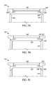
- FIGS. 5 A-C illustrate various configurations of the wafer carrier and the rotating tube according to the present teaching that includes a beveled interface which provides self-centering of the wafer carrier to the rotation axis of the rotating tube.
- FIG. 6A illustrates a self-centering wafer carrier CVD system according to the present teaching at room temperature.
- FIG. 6B illustrates a self-centering wafer carrier CVD system according to the present teaching at process temperature.
- FIG. 6C illustrates a self-centering wafer carrier CVD system according to the present teaching at a temperature that is higher than process temperature.
- FIG. 7 illustrates a self-centering wafer carrier of the present teaching comprising spacers and relief structure.
- FIG. 8A illustrates an embodiment of a self-centering wafer carrier CVD system of the present teaching comprising an open-carrier design.
- FIG. 8B illustrates an embodiment of a self-centering wafer carrier CVD system of the present teaching comprising an open-carrier design and a beveled edge.
- FIG. 8C illustrates an embodiment of a self-centering wafer carrier CVD system of the present teaching comprising an open-carrier and positive purge design.
- FIG. 8D illustrates an embodiment of a self-centering wafer carrier CVD system of the present teaching comprising an open-carrier with a simple separator.
- FIG. 8E illustrates an embodiment of a self-centering wafer carrier CVD system of the present teaching comprising an open-carrier with a centrally located separator.
- FIG. 8F illustrates an embodiment of a self-centering wafer carrier CVD system of the present teaching comprising an open-carrier with a static separator.
- FIG. 8G illustrates an embodiment of a self-centering wafer carrier CVD system of the present teaching comprising an open-carrier with a removable quartz separator.
- FIG. 8H illustrates another embodiment of a self-centering wafer carrier CVD system of the present teaching comprising an open-carrier design and a beveled edge.
- FIG. 8I illustrates another embodiment of a self-centering wafer carrier CVD system of the present teaching comprising an open-carrier and positive purge design.
- FIG. 8J illustrates another embodiment of a self-centering wafer carrier CVD system of the present teaching comprising an open-carrier with a simple separator.
- FIG. 8K illustrates another embodiment of a self-centering wafer carrier CVD system of the present teaching comprising an open-carrier with a centrally located separator.
- FIG. 8L illustrates another embodiment of a self-centering wafer carrier CVD system of the present teaching comprising an open-carrier with a static separator.
- FIG. 8M illustrates another embodiment of a self-centering wafer carrier CVD system of the present teaching comprising an open-carrier with a removable quartz separator.
- FIG. 9A illustrates a self-centering wafer carrier CVD system of the present teaching with a pocketless wafer carrier that has an edge with a bevel geometry and a rim.
- FIG. 9B illustrates a self-centering wafer carrier CVD system of a pocketless wafer carrier according to the present teaching at room temperature.
- FIG. 10 shows other details of various embodiments of the post and the contact interface shown in FIGS. 9A and 9B including details of the wafer, the wafer carrier, and the post interface of the wafer carrier.
- FIG. 11 shows yet other details of various embodiments of the post and the contact interface as shown in FIGS. 9A and 9B including details of the wafer, the wafer carrier, and the post interface of wafer carrier.
- FIG. 12 shows other details of various embodiments of bumper and contact interface as in FIGS. 4A, 5A -C, and 6 A including details of the wafer, the wafer carrier, and bumper interface of wafer carrier.
- FIG. 13 shows other details of various embodiments of bumper and contact interface as in FIGS. 4A, 5A -C, and 6 A including details of wafer, wafer carrier, and the bumper interface of the wafer carrier.
- FIG. 14 shows an isometric view of a wafer carrier having a pocket having one or more bumpers.
- FIG. 15 shows a plan view of a pocketless wafer carrier according to the present teaching.
- FIG. 15A is a cross-section view of the pocketless wafer carrier of FIG. 15 along line A-A.
- FIG. 15B is an isometric view of the pocketless wafer carrier of FIG. 15 .
- FIG. 16 shows a plan view of another pocketless wafer carrier according to the present teaching.
- FIG. 16A is a cross-section of the pocketless wafer carrier of FIG. 16 along line A-A.
- FIG. 16B is an isometric view of the pocketless wafer carrier of FIG. 16 .
- FIG. 17 is a cross-section view of a wafer support ring mounted on rotating drum according to the present teaching.
- FIG. 17A illustrates an enlarged portion of FIG. 17 .
- FIG. 18 illustrates an isometric view of a wafer support ring.
- FIG. 19 illustrates an expanded top-view of a single substrate carrier, according to the present teaching.
- FIG. 20 illustrates an isometric view of another wafer support ring embodiment according to the present teaching.
- FIG. 20A illustrates a cross-section of the wafer support ring of FIG. 20 along line A-A.
- FIG. 21 illustrates a cross-section of the wafer support ring of FIG. 20 mounted on a rotating drum according to the present teaching.
- FIG. 21A illustrates an enlarged portion of FIG. 21 .
- FIG. 22 illustrates an exploded view of the wafer support ring and rotating drum of FIG. 21 according to the present teaching.
- the present teaching relates to methods and apparatuses for self-centering a wafer carrier for CVD and other types of processing reactors. Aspects of the present teaching are described in connection with a single wafer carrier. However, one skilled in the art will appreciate that many aspects of the present teachings are not limited to a single wafer carrier.
- FIG. 1 illustrates one embodiment of a single wafer CVD reactor 100 of the present teaching comprising a wafer carrier 102 and rotating tube 104 with a multi-zone heater assembly 106 .
- the wafer carrier 102 is supported at the perimeter by a rotating tube 104 .
- a multi-zone heating assembly 106 is positioned under the wafer carrier 102 inside the rotating tube 104 .
- there is a diametral gap between the wafer carrier 102 and the rotating tube 104 that allows for carrier loading. The width of this gap changes during heating because the wafer carrier 102 and the rotating tube 104 have different coefficients of thermal expansion (CTE) resulting in different expansions as a function of temperature.
- CTE coefficients of thermal expansion
- Wafer carriers and rotating tubes can be formed from a variety of materials such as, for example, silicon carbide (SiC), boron nitride (BN), boron carbide (BC), aluminum nitride (AlN), alumina (Al 2 O 3 ), sapphire, silicon, gallium nitride, gallium arsenide, quartz, graphite, graphite coated with silicon carbide (SiC), other ceramic materials, and combinations thereof.
- these and other materials can have a refractory coating, for example, a carbide, nitride or oxide refractory coating.
- the wafer carrier and rotating tubes can be formed from refractory metals, such as molybdenum, tungsten, and alloys thereof.
- refractory metals such as molybdenum, tungsten, and alloys thereof.
- CTE coefficient of thermal expansion
- quartz which is commonly used as the rotating tube, is ⁇ 5.5 ⁇ 10 ⁇ 7 ° C. ⁇ 1 .
- CVD SiC is ⁇ 4.5 ⁇ 10 ⁇ 6 ° C. ⁇ 1 .
- an initial gap between the wafer carrier and the rotating tube at room temperature of about 0.5 mm reduces to about 0.05 mm at 1100° C.
- a small gap at high operating temperatures is required to maintain the integrity of the quartz tube.
- known wafer carrier designs do not spin around the geometrical center of the wafer carrier as the temperature increases. This leads to a linear, or asymmetric, temperature distribution along the wafer carrier radius. Asymmetric temperature non-uniformities cause deposition uniformities which cannot be compensated by multi-zone heating systems. Consequently, known wafer carriers for CVD reactors suffer from non-uniform asymmetric temperature profiles which result from the wafer carrier not rotating around its geometrical center.
- FIG. 2A illustrates a diagram of a CVD reactor that does not use a self-centering technique.
- FIG. 2A illustrates both a side-view and a plan-view of the relative positions of a wafer carrier, rotation axis, and heater for a CVD reactor 200 for a configuration where the wafer carrier center axis 202 is not coincident with the rotation axis 204 of the rotating tube.
- a wafer carrier center axis which is also sometimes referred to as a central axis, is defined herein as a line centered at the mid-point of the carrier, and extending in a direction normal to the top of the wafer carrier.
- the wafer carrier center axis 202 is offset from the rotation axis 204 of the rotating tube (not shown) and both the wafer carrier center axis 202 and the rotation axis 204 of the rotating tube are offset from the heater center 206 . Consequently, when the wafer carrier is rotated, the point A 210 and point B 212 travel in different concentric circular paths. More specifically, the point A 210 moves from one far edge of the rotation tube to another far edge as shown by the position of points A′ 210 ′ and A′′ 210 ′′.
- the point B 212 which is closer to the rotation axis 204 moves from a more inner point of the rotation tube to another more inner point as shown by the position of points B′ 212 ′ and B′′ 212 ′′.
- the two points A 210 and B 212 experience different average temperatures on rotation, which leads to an asymmetric temperature profile 208 .
- the asymmetric temperature profile 208 shows a higher temperature on one edge of the wafer, coincident with point B 212 as compared to the temperature on the opposite edge of the wafer coincident with point A 210 .
- the average temperature of point A 210 , T a is less than the average temperature of point B 212 , T b , which creates a tilted asymmetric temperature profile 208 .
- the asymmetric temperature profile 208 shows a higher temperature on the edge at point B 212 of the wafer as compared to the temperature on the opposite edge of the wafer at point A 210 .
- the resulting temperature profile is asymmetric with respect to the rotation axis. Even in configurations where the carrier axis is coincident with the heater axis, wafer motion eccentricity owing to an offset between the carrier axis and the rotation axis still leads to asymmetric temperature non-uniformity.
- FIG. 2B illustrates a diagram of an embodiment of a CVD reactor with self-centering according to the present teaching.
- FIG. 2B illustrates a side-view and plan-view of the relative positions of a wafer carrier, rotation axis, and heater for a CVD reactor 250 in the configuration where the wafer carrier center axis 252 is coincident with the rotation axis 254 .
- Coincident alignment of the wafer carrier center axis and the rotation axis as described herein means that the two axes fall on the same line.
- the position of the wafer carrier center axis 252 relative to the rotation axis 254 of the rotating tube (not shown) is coincident, but offset from the heater center 256 .
- the point A 260 and the point B 262 experience the same average temperature from the heater.
- the point C 264 and the point D 266 also experience the same average temperature.
- the average temperature at points C 264 and D 266 are different from the average temperature of points A 260 and B 262 .
- the resulting temperature profile 258 is axially symmetric, but non-uniform.
- the uniformity of a film deposited with an axially symmetric non-uniform temperature profile 258 resulting from a self-centering wafer carrier of the present teaching can be improved by properly configuring and operating a multi-zone heater positioned proximate to the wafer carrier.
- the film uniformity resulting from axially symmetric non-uniform temperature profile 258 of the present teaching can be improved by carrier pocket profiling for wafer temperature uniformity. See, for example, U.S. Pat. No. 8,486,726, entitled “Method for Improving Performance of a Substrate Carrier”, which is assigned to the present assignee.
- FIG. 3A illustrates a thermal profile 300 across the surface of a circular wafer resulting from rotation eccentricity in a CVD reactor for a 1.33 mm induced eccentricity.
- FIG. 3B illustrates the temperature gradient as a function of radius 310 at 0° 312 and 90° 314 for the same 1.33 mm induced eccentricity as shown in FIG. 3A .
- FIG. 3B illustrates a large linear temperature distribution along the radius of the carrier. Such a linear temperature distribution cannot be easily compensated for because known multi-zone heating system alone will not compensate for linear temperature distributions. The linear temperature distribution results in low deposition uniformity.
- FIG. 3C illustrates a thermal profile 320 across a circular wafer resulting from rotation eccentricity in a CVD reactor for a 0.33 mm induced eccentricity.
- FIG. 3D illustrates the temperature gradient as a function of radius 330 at 0° 332 and 90° 334 for the same 0.33 mm induced eccentricity.
- FIG. 3E illustrates a resulting plot of a temperature gradient 340 as a function of carrier rotation eccentricity based on the data from FIGS. 3A-D . The plot indicates that the gradient 340 is reduced to less than approximately 2° C. when carrier rotation eccentricity is less than 0.33 mm.
- a wafer carrier according to the present teaching can provide coincidence of the wafer carrier central axis and the rotation axis of the rotating tube at process temperature. This coincidence reduces eccentricity of the circular rotation of the wafer, in order to create an axially symmetric temperature profile that can be compensated for by properly using multi-zone heating elements.
- FIG. 4A illustrates a self-centering wafer carrier CVD system of the present teaching 400 with a wafer carrier 402 that has an edge 404 with a bevel geometry and a flat rim 406 .
- the edge 404 of the wafer carrier 402 corresponds to a circular region at or near the outer perimeter of the wafer carrier. The edge protrudes from the lower surface of the wafer carrier.
- a wafer 408 is centered on the upper surface of the wafer carrier 402 .
- a heating element 410 is located under the wafer carrier 402 .
- the wafer 408 , positioned in pocket 420 , rim 406 , and heating element 410 are all positioned in parallel.
- the edge of wafer 408 contacts sidewall 424 of pocket 420 at contact interface 421 , which is discussed further below.
- the wafer carrier 402 is positioned on a rotating tube 412 .
- the rotating tube 412 has an edge 414 with a beveled geometry and a flat rim 416 .
- the wafer carrier edge 404 and the rotating tube edge 414 are proximate and parallel when the wafer carrier 402 is positioned on the rotating tube 412 .
- the bevel geometry on the edge 414 of the rotating tube 412 is formed at an angle ⁇ 418 with respect to the rotation axis of the rotating tube 412 .
- the bevel geometry on the edge 404 of the wafer carrier 402 is set at an angle ⁇ 418 with respect to the center-axis of the carrier that runs normal to the upper surface of the wafer carrier that supports the wafer.
- the angle ⁇ 418 is chosen such that tan( ⁇ )>f, where f is the coefficient of friction between the wafer carrier and rotation tube materials.
- FIG. 4B illustrates a self-centering wafer carrier CVD system of the present teaching 430 where the wafer carrier 432 has been transferred into the process reactor (not shown) and positioned on the rotating tube 434 at room temperature before the deposition process begins.
- FIG. 4B illustrates a gap 436 , with width L, and the rotating tube diameter 438 , of width D.
- One feature of the wafer carrier of the present teaching is that the wafer carrier edge is dimensioned such that there is a gap between the edge of the rotating tube and the edge of the wafer carrier at room temperature.
- the dimensions of the wafer carrier 432 and the rotating tube 434 are selected such that the gap 436 satisfies the following equation: L ⁇ (CTE carrier ⁇ CTE tube )* D*T, where CTE carrier is the coefficient of thermal expansion of the carrier 432 , and CTE tube is the coefficient of thermal expansion of the rotating tube 434 , and T is the process temperature.
- the gap 436 according to the above equation will decrease with increasing operating temperature, and just before the process temperature is realized, the gap will be substantially zero.
- FIG. 4C illustrates a self-centering wafer carrier CVD system of the present teaching 450 in the configuration described in connection with FIG. 4B , but at process temperature.
- the near contact between the beveled edges of the wafer carrier 452 and the rotating tube 454 result in a centering of the carrier on the rotating tube. Consequently, the wafer carrier center axis and the axis of rotation are coincident.
- FIGS. 5A-C illustrate various configurations of the wafer carrier and the rotating tube according to the present teaching that includes various beveled geometry edges of the wafer carrier and the rotating tube and resulting interface between the wafer carrier and rotating tube which provides self-centering of the wafer carrier central axis and the rotation axis of the rotating tube.
- FIG. 5A illustrates a first configuration 500 of the wafer carrier 502 including a first edge 506 that is positioned on the wafer carrier 502 proximate to the outer perimeter of the wafer carrier 502 .
- the edge 506 of the wafer carrier 502 is formed with a beveled geometry and runs circularly around the center of the wafer carrier 502 .
- An edge 508 is positioned on the rotating tube 504 proximate to the outer edge of the rotating tube 504 .
- the edge 508 of the rotating tube 504 is formed with a beveled geometry and runs circularly around the perimeter of the rotating tube 504 .
- the beveled geometry of the edge 506 of the wafer carrier 502 and the beveled geometry of the edge 508 of the rotating tube 504 are proximate and parallel when the wafer carrier 502 is positioned on the rotating tube 504 .
- the beveled edge is formed on the outer perimeter of the rotating tube 504 .
- the beveled edge of the rotating tube 504 is formed on the inner perimeter of the rotating tube 504 .
- FIG. 5A the beveled geometry of the edge 506 of the wafer carrier 502 and the beveled geometry of the edge 508 of the rotating tube 504 are proximate and parallel when the wafer carrier 502 is positioned on the rotating tube 504 .
- the beveled edge is formed on the outer perimeter of the rotating tube 504 .
- the beveled edge of the rotating tube 504 is formed on the inner perimeter of the rotating tube 504 .
- the wafer carrier 502 is positioned on the rotating tube 504 such that the beveled geometry of the edge 506 of the wafer carrier 502 and the beveled geometry of the edge 508 of the rotating tube 504 are in near contact, thereby creating self-centering of the wafer 510 during processing because the beveled edges 506 , 508 keep the axis of rotation of the rotating tube 504 coincident with the wafer carrier center.
- FIG. 5B illustrates a second configuration 530 of the wafer carrier 532 and rotating tube 534 that includes an edge 536 with a beveled geometry that is positioned on the wafer carrier 532 and an edge 538 with a beveled geometry that is positioned on the rotating tube 534 .
- the beveled edge 536 formed on the wafer carrier 532 and the beveled edge 538 formed on the rotating tube 534 are angled up and away from the inner perimeter of the rotating tube 534 .
- the two beveled edges are parallel.
- the wafer carrier 532 is positioned on the rotating tube 534 such that the first beveled edge 536 and the second beveled edge 538 are in near contact, such that the wafer 540 is centered over the rotation axis during processing.
- the beveled edges 536 , 538 keep the axis of rotation of the rotating tube 534 coincident with the wafer carrier center axis.
- FIG. 5C illustrates a third configuration 550 of the wafer carrier 552 and rotating tube 554 that includes a first beveled edge 556 that is positioned on the wafer carrier 552 and a second beveled edge 558 positioned on the rotating tube 554 .
- the first beveled edge 556 and the second beveled edge 558 are angled down and away from the inner perimeter of the rotating tube.
- the two beveled edges are parallel.
- the wafer carrier 552 is positioned on the rotating tube 554 such that the first beveled edge 556 and the second beveled edge 558 are in near contact, creating self-centering of the wafer 560 during processing.
- the beveled edges 556 , 558 keep the axis of rotation of the rotating tube 554 coincident with the wafer carrier 552 center axis.
- One feature of the present teaching is that the geometry of the edge of the wafer carrier and the geometry of the edge of the rotating tube create a particular amount of eccentric or nearly eccentric rotation of the wafer during processing at process temperature.
- the amount of eccentric or nearly eccentric rotation of the wafer during processing is chosen to achieve a desired process temperature profile that results in a highly uniform film thickness profile.
- FIG. 6A illustrates a self-centering wafer carrier CVD system 600 according to the present teaching showing wafer 620 positioned in pocket 624 at room temperature.
- the edge of wafer 620 contacts sidewall 626 of pocket 624 at contact interface 621 , which is discussed further below.
- the edge 602 of the wafer carrier 604 in this embodiment is parallel with the center axis 606 of the wafer carrier 604 , and is also parallel with the edge 608 of the rotating tube 610 .
- the geometry of the wafer carrier edge 602 is such that a gap 612 exists between the edge 602 of the wafer carrier 604 and the edge 608 of the rotating tube 610 .
- the gap 612 allows enough room for expansion of the wafer carrier 604 relative to the rotating tube 610 so that no contact occurs between the wafer carrier edge 602 and the rotating tube edge 608 .
- the wafer carrier 604 remains smaller than the rotating tube 610 throughout the entire process temperature cycle, and in particular at the highest process temperature.
- a heater 614 is centered along the axis of rotation 616 of the rotating tube 610 .
- FIG. 6A shows that the center axis 606 of the wafer carrier 604 is not coincident with the axis of rotation 616 .
- a spacer 618 is dimensioned such that at a process temperature, the wafer carrier center axis and the axis of rotation of rotating tube 610 are coincident.
- the spacer 618 is machined into the wafer carrier edge 602 making it integral with its structure.
- the wafer carrier 604 is graphite, and the spacer 618 is machined directly into the graphite and the entire wafer carrier 604 is then coated with a different material, such as silicon carbide (SiC).
- SiC silicon carbide
- two or more spacers are used to form a stable contact with the edge 608 of the rotating tube 610 .
- FIG. 6B illustrates a self-centering wafer carrier CVD system 630 according to the present teaching showing wafer 620 positioned in pocket 624 at process temperature.
- the edge of wafer 620 contacts sidewall 626 of pocket 624 at contact interface 621 , which is discussed further below.
- FIG. 6B shows that the center of the wafer carrier 632 is aligned directly with the center of the axis of rotation 634 of the rotating tube 636 when the wafer carrier 632 is at the operating conditions. Thus, there is no eccentric rotation of the wafer during processing at process temperature.
- FIG. 6C illustrates a self-centering wafer carrier CVD system 670 according to the present teaching showing wafer 620 positioned in pocket 624 at a temperature that is higher than the process temperature.
- the edge of wafer 620 contacts the sidewall of pocket 624 at contact interface 621 , which is discussed further below.
- FIG. 6C shows that at temperatures higher than the process temperature, the center axis 672 of the wafer carrier 674 is no longer aligned with the axis of rotation 676 .
- the spacer 678 is used to offset the eccentricity caused by the offset between the center of the wafer carrier 672 and the axis of rotation 676 to provide a symmetric temperature profile at these higher process temperatures.
- FIG. 7 illustrates a self-centering wafer carrier 700 of the present teaching with an edge geometry that includes one or more spacers 702 positioned on the circular region that corresponds to the edge of the wafer carrier, and a relief structure 704 positioned opposite to the one or more spacers 702 .
- the relief structure 704 includes one or more flat sections that are diametrically opposed to spacers 702 .
- the relief structure 704 shifts the center of mass of the wafer carrier 700 .
- the centrifugal force of the rotating mass helps to overcome the friction between the edge of the wafer carrier 700 , and the edge of the rotating tube (not shown in FIG. 7 ).
- the centrifugal force moves the wafer carrier 700 in a direction such that the one or more spacers 702 remain in contact with the edge of the rotating tube.
- FIGS. 8A-C illustrate embodiments of a self-centering wafer carrier CVD system 800 of the present teaching with an open-carrier design.
- open carrier design we mean that portions of the wafer 802 are open or unsupported. Only a small region around the perimeter of the wafer is in physical contact with the wafer carrier.
- a separator plate is used to define the region inside the rotating tube to which the backside of the wafer is exposed.
- FIG. 8A illustrates an open-carrier design with a separator plate 806 .
- the wafer 802 is supported by the wafer carrier 804 at the perimeter of the wafer 802 , leaving both the top and the bottom of the wafer 802 exposed to the atmosphere in the chamber above and below the wafer.
- FIG. 8B illustrates an embodiment of a self-centering carrier CVD system 830 of the present teaching with a wafer carrier 832 that comprises an open-carrier design and a geometry with a beveled edge 834 .
- the beveled edge 834 of the wafer carrier rests on a beveled edge 836 of the rotating tube 838 when the wafer carrier 832 is positioned on the rotating tube 838 .
- the interface between the two beveled edges 834 , 836 centers the wafer carrier 832 with respect to the rotation axis of the rotating tube 838 .
- FIG. 8C illustrates an embodiment of a self-centering wafer carrier CVD system 870 of the present teaching with a vertical, tangential lock 872 for the separator plate 874 .
- the embodiment illustrated in FIG. 8C is designed for positive purge 876 in the cavity above the separator plate.
- the purge gases are provided to the region between the separator plate 874 and the wafer 878 by a tube 880 that passes through the separator plate 874 .
- the bottom side of the wafer 878 is exposed to the purge gasses.
- the open-carrier design wafer carriers utilize various geometries and dimensions of the wafer carrier edge and the rotating tube edge that provides self-centering of the wafer carrier to the rotation axis of the rotating tube.
- FIG. 8D illustrates an embodiment of a self-centering wafer carrier CVD system 820 of the present teaching comprising an open-carrier 821 with a simple separator 822 .
- the separator 822 prevents refractory metals, such as tungsten, from depositing on the backside of the wafer 824 .
- the separator 822 provides radiant heating to the wafer 824 .
- the separator 822 is made from silicon carbide, quartz, or other material. Using silicon carbide provides relatively low temperature ramp rates because silicon carbide has a high thermal conductivity.
- the separator 822 may be formed from non-transparent material to minimize cleaning requirements. Also, the separator 822 can include a beveled edge 826 to provide self-centering.
- both the wafer carrier 821 and the separator 822 utilize self-centering geometries and dimensions of the respective edges in order to prevent non-uniform temperature profiles during deposition.
- a purge tube 828 is used to provide positive pressure purge gas 829 to the cavity.
- FIG. 8E illustrates an embodiment of a self-centering wafer carrier CVD system of the present teaching comprising an open-carrier 841 with a centrally-located separator 842 .
- the separator 842 is centered on a quartz buffer 843 using a brace 844 that also serves as a purge tube.
- the brace 844 provides self-centering of the separator 842 to the rotation axis of the rotating tube 846 .
- the edge dimension and geometry of the wafer carrier 841 provides self-centering of the wafer carrier 841 to the rotation axis of the rotating tube 846 .
- the separator 842 may be formed from non-transparent material to minimize cleaning requirements.
- FIG. 8F illustrates an embodiment of a self-centering wafer carrier CVD system 850 of the present teaching comprising an open-carrier 851 with a static separator 852 .
- the umbrella-shaped static separator 852 has two edges 853 , 853 ′ that cause the separator 852 to remain static with respect to the rotating tube 854 during rotation. In other words, the static separator 852 does not rotate with the rotating tube 854 during operation.
- the dimension and geometry of the static separator 852 is chosen to minimize stresses that arise because of the temperature differences between the top and the bottom for the static separator 852 .
- the static separator 852 is made from silicon carbide, quartz, or other material.
- the static separator 852 may be formed from non-transparent material to minimize cleaning requirements.
- the static separator 852 prevents refractory metals, such as tungsten, from depositing on the backside of the wafer 855 .
- FIG. 8G illustrates an embodiment of a self-centering wafer carrier CVD system 860 of the present teaching comprising an open-carrier 861 and a quartz separator 862 .
- the quartz separator 862 may be permanent or removable.
- the quartz separator 862 prevents refractory metals, such as tungsten, from depositing on the backside of the wafer 863 .
- the separator 862 may be a continuous piece of quartz with the rotating tube 864 . This continuous-piece design eliminates the issue of centering the separator, since the separator is part of the rotating structure.
- a non-transparent silicon carbide carrier 861 blocks stray light.
- the dimensions and geometry of the separator 862 is chosen to avoid stresses due to thermal gradients.
- FIG. 8H illustrates an embodiment of a self-centering carrier CVD system 930 of the present teaching with a wafer carrier 932 that comprises an open-carrier design and geometry with a beveled edge 934 .
- the beveled edge 934 of the wafer carrier rests on a beveled edge 936 of the rotating tube 938 when the wafer carrier 932 is positioned on the rotating tube 938 .
- the interface between the two beveled edges 934 , 936 centers the wafer carrier 932 with respect to the rotation axis of the rotating tube 938 .
- FIG. 8I illustrates an embodiment of a self-centering wafer carrier CVD system 940 of the present teaching with a vertical, tangential lock 942 for the separator plate 944 .
- the embodiment illustrated in FIG. 8I is designed for positive purge 946 in the cavity above the separator plate.
- the purge gases are provided to the region between the separator plate 944 and the wafer 948 by a tube 945 that passes through the separator plate 944 .
- the bottom side of the wafer 948 is exposed to the purge gasses.
- the open-carrier design wafer carriers utilize various geometries and dimensions of the wafer carrier edge and the rotating tube edge that provides self-centering of the wafer carrier to the rotation axis of the rotating tube 987 .
- FIG. 8J illustrates an embodiment of a self-centering wafer carrier CVD system 980 of the present teaching comprising an open-carrier 981 with a simple separator 982 .
- the separator 982 prevents refractory metals, such as tungsten, from depositing on the backside of the wafer 984 .
- the separator 982 provides radiant heating to the wafer 984 .
- the separator 982 is made from silicon carbide, quartz, or other material. Using silicon carbide provides a relatively high temperature ramp rates because silicon carbide has a high thermal conductivity.
- the separator 982 may be formed from non-transparent material to minimize cleaning requirements. Also, the separator 982 can include a beveled edge 986 to provide self-centering.
- both the wafer carrier 981 and the separator 982 utilize self-centering geometries and dimensions of the respective edges in order to prevent non-uniform temperature profiles during deposition.
- a purge tube 988 is used to provide positive pressure purge gas 989 to the cavity.
- FIG. 8K illustrates an embodiment of a self-centering wafer carrier CVD system 990 of the present teaching comprising an open-carrier 991 with a centrally-located separator 992 .
- the separator 992 is centered on a quartz buffer 993 using a brace 994 that also serves as a purge tube.
- the brace 994 provides self-centering of the separator 992 to the rotation axis of the rotating tube 996 .
- the edge dimension and geometry of the wafer carrier 991 provides self-centering of the wafer carrier 991 to the rotation axis of the rotating tube 996 .
- the separator 992 may be formed from non-transparent material to minimize cleaning requirements.
- FIG. 8L illustrates an embodiment of a self-centering wafer carrier CVD system 1300 of the present teaching comprising an open-carrier 1301 with a static separator 1302 .
- the umbrella-shaped static separator 1302 has two edges 1303 , 1303 ′ that cause the separator 1302 to remain static with respect to the rotating tube 1304 during rotation. In other words, the static separator 1302 does not rotate with the rotating tube 1304 during operation.
- the dimension and geometry of the static separator 1302 is chosen to minimize stresses that arise because of the temperature differences between the top and the bottom for the static separator 1302 .
- the static separator 1302 is made from silicon carbide, quartz, or other material.
- the static separator 1302 may be formed from non-transparent material to minimize cleaning requirements.
- the static separator 1302 prevents refractory metals, such as tungsten, from depositing on the backside of the wafer 1305 .
- FIG. 8M illustrates an embodiment of a self-centering wafer carrier CVD system 1310 of the present teaching comprising an open-carrier 1311 and a quartz separator 1312 .
- the quartz separator 1312 may be permanent or removable.
- the quartz separator 1312 prevents refractory metals, such as tungsten, from depositing on the backside of the wafer 1313 .
- the separator 1312 may be a continuous piece of quartz with the rotating tube 1314 . This continuous-piece design eliminates the issue of centering the separator, since the separator is part of the rotating structure.
- a non-transparent silicon carbide carrier 1311 blocks stray light.
- the dimensions and geometry of the separator 1312 is chosen to avoid stresses due to thermal gradients.
- FIG. 9A illustrates a self-centering pocketless wafer carrier CVD system 900 of the present teaching with a wafer carrier 902 that has an edge 904 with a bevel geometry and a flat rim 906 .
- the edge 904 of the wafer carrier 902 corresponds to a circular region at or near the outer perimeter of the wafer carrier. The edge protrudes from the lower surface of the wafer carrier.
- a wafer 908 is centered on the upper surface of the wafer carrier 902 by post 920 . The edge of wafer 908 and post 920 contact at contact interface 921 , which is discussed further below.
- a heating element 910 is located under the wafer carrier 902 .
- the wafer 908 , rim 906 , and heating element 910 are all positioned in parallel.
- the wafer carrier 902 is positioned on a rotating tube 912 .
- the rotating tube 912 has an edge 914 with a beveled geometry and a flat rim 916 .
- the wafer carrier edge 904 and the rotating tube edge 914 are proximate and parallel when the wafer carrier 902 is positioned on the rotating tube 912 .
- the bevel geometry on the edge 914 of the rotating tube 912 is formed at an angle ⁇ 918 with respect to the rotation axis of the rotating tube 912 .
- the bevel geometry on the edge 904 of the wafer carrier 902 is set at an angle ⁇ 918 with respect to the center-axis of the carrier that runs normal to the upper surface of the wafer carrier that supports the wafer.
- the angle ⁇ 918 is chosen such that tan( ⁇ )> ⁇ , where ⁇ is the coefficient of friction between the wafer carrier and rotation tube materials.
- the wafer carrier 902 does not have a pocket and can be considered to be a pocketless carrier where the posts 920 retain wafer 908 on wafer carrier 904 during operation.
- FIG. 9B illustrates a self-centering pocketless wafer carrier CVD system 950 according to the present teaching at room temperature.
- the edge 952 of the wafer carrier 954 in this embodiment is parallel with the center axis 956 of the wafer carrier 954 , and is also parallel with the edge 958 of the rotating tube 960 .
- the geometry of the wafer carrier edge 952 is such that a gap 968 exists between the edge 952 of the wafer carrier 954 and the edge 958 of the rotating tube 960 .
- the gap 968 allows enough room for expansion of the wafer carrier 954 relative to the rotating tube 960 so that no contact occurs between the wafer carrier edge 952 and the rotating tube edge 958 .
- the wafer carrier 954 remains smaller than the rotating tube 960 throughout the entire process temperature cycle, and in particular at the highest process temperature.
- a heater 964 is centered along the axis of rotation 966 of the rotating tube 960 .
- FIG. 9B shows that the center axis 956 of the wafer carrier 954 is not coincident with the axis of rotation 966 .
- a spacer 962 is dimensioned to make the rotation of the wafer carrier 954 eccentric where wafer 970 is within the circle that represents the rotating tube 960 .
- Wafer 970 is centered on wafer carrier 954 by post 972 .
- the edge of wafer 970 and post 972 contact at contact interface 971 , which is discussed further below.
- the spacer 962 is machined into the wafer carrier edge 952 making it integral with its structure.
- the wafer carrier 954 is graphite, and the spacer 962 is machined directly into the graphite and the entire wafer carrier 954 is then coated with a different material, such as silicon carbide (SiC).
- SiC silicon carbide
- two or more spacers are used to form a stable contact with the edge 958 of the rotating tube 960 .
- the system shown in FIG. 9B is similar to that shown in FIG. 6A above and when the system of FIG. 9B rotates, it will essentially follow the description set out for FIGS. 6B and 6C above.
- the wafer carrier 954 does not have a pocket and can, therefore, be considered to be a pocketless carrier where the posts 972 retain wafer 970 on wafer carrier 954 during operation.
- FIGS. 10 and 11 show details of post 920 or 972 and contact interface 921 or 971 as shown in FIGS. 9A and 9B above. See dotted circles F and G, respectively.
- item 1100 shows the detail of wafer, wafer carrier, and post interface of wafer carrier 902 or 954 mentioned above.
- Item 1102 is post 920 or 972 mentioned above.
- Item 1106 is a portion of wafer carrier 902 or 954 , respectively, on which wafer 908 or 970 , respectively, rests.
- Item 1104 is a wall of post 920 or 972 that forms the contact interface 921 or 971 where wafer 908 or 970 , respectively, contacts post 920 or 972 (similar to item 1102 ).
- the face of item 1104 which interfaces with the wafer edge, can be flat or curved (for example, convex).
- surface 1200 shows the detail of the wafer, the wafer carrier, and the post interface of the wafer carrier 902 or 954 described in connection with FIGS. 9A, 9B , respectively.
- Surface 1202 is the post 920 or 972 .
- surface 1204 is an undercut wall of the post 920 or 972 that forms contact interface 921 or 971 , related to FIGS. 9A and 9B , respectively.
- Surface 1206 is a portion of the wafer carrier 902 or 954 , respectively, on which the wafer 908 or 970 , respectively, rests.
- Surface 1204 and surface 1206 form an angle ⁇ , which can range from about 80° to about 95°.
- FIGS. 12 and 13 show details of various embodiments of sidewalls and contact interface 421 or 621 as described in connection with FIGS. 4A and 6A .
- surface 1900 shows the detail of the wafer carrier and the sidewall of the wafer carrier 402 or 604 described in connection with FIGS. 4A and 6A .
- Surface 1902 is the top face of wafer carrier 402 or 604 as shown in FIGS. 4A and 6A .
- Surface 1906 is a portion of pocket 420 or 624 of wafer carrier 402 or 604 , respectively, on which wafer 408 or 620 , respectively, rests.
- Surface 1904 is a bumper formed in the sidewall 424 or 626 of wafer carrier 402 or 604 , respectively, which forms contact interface 421 or 621 when wafer 408 or 620 , respectively, is placed in pocket 420 or 624 .
- the face of item 1904 which interfaces with the wafer edge, can be flat or curved (for example, convex).
- item 1800 shows the detail of wafer carrier and sidewall of wafer carrier 402 or 604 described in connection with FIGS. 4A and 6A .
- Surface 1802 is the top face of wafer carrier 402 or 604 as mentioned above.
- surface 1804 is a bumper formed in the sidewall 424 or 626 of wafer carrier 402 or 604 , respectively and is undercut so as to form contact interface 421 or 621 , as shown in FIGS. 4A and 6A , respectively.
- Item 1806 is a portion of pocket 420 or 624 of wafer carrier 402 or 604 , respectively, on which wafer 408 or 620 , respectively, rests.
- Surface 1804 and surface 1806 form an angle ⁇ , which can range from about 80° to about 95°.
- the entire sidewall 424 or 626 of FIGS. 4A and 6A are not undercut.
- the undercut portion of pocket 420 or 624 is only formed when bumpers are formed within the respective pockets.
- FIG. 14 shows an isometric view of a wafer carrier 1600 having a pocket 1602 having one or more bumpers 1604 , such as the bumpers described in connection with FIGS. 12 and 13 .
- the wall 1606 of pocket 1602 has one or more bumpers 1604 formed on it.
- FIG. 15 shows plan view of another pocketless wafer carrier 1400 according to the present teaching.
- Pocketless wafer carrier 1400 has rim 1402 and posts 1404 .
- Posts 1404 are similar to those posts described in FIGS. 10 and 11 .
- Pocketless wafer carrier 1400 has surface 1408 on which wafer 1406 rests.
- FIG. 15A shows a cross-sectional view of pocketless wafer carrier 1400 .
- Pocketless wafer carrier 1400 has an edge 1410 having a bevel geometry and a rim 1402 , similar to the edge and rim as described in connection with FIG. 4A .
- the bevel geometry of edge 1410 forms a similar angle ⁇ , similar to angle ⁇ 418 described in connection with 4 A, with a rotating tube of a reactor in which pocketless wafer carrier 1400 is utilized.
- the rotating tube is similar to the rotating tube 412 described in connection with FIG. 4A .
- FIG. 15B shows an isometric view of pocketless wafer carrier 1400 according to the present teaching.
- the pocketless wafer carrier 1400 has rim 1402 and posts 1404 .
- Posts 1404 are similar to those posts described in connection with FIGS. 10 and 11 .
- the pocketless wafer carrier 1400 has surface 1408 on which a wafer (not shown) rests.
- FIG. 16 shows a plan view of another pocketless wafer carrier 1500 according to the present teaching.
- Pocketless wafer carrier 1500 has rim 1502 and posts 1504 , which are similar to posts described in FIGS. 10 and 11 .
- Pocketless wafer carrier 1500 has surface 1508 on which a wafer 1506 rests.
- FIG. 16A shows a cross-section of pocketless wafer carrier 1500 .
- Pocketless wafer carrier 1500 has an edge 1510 having a bevel geometry and a rim 1502 , similar to the edge and rim as described in connection with FIG. 4A .
- the bevel geometry of edge 1510 forms a similar angle ⁇ , similar to angle ⁇ 418 as described above, with a rotating tube of a reactor in which pocketless wafer carrier 1500 is utilized.
- the rotating tube is similar to the rotating tubes described herein, such as rotating tube 412 .
- FIG. 16B shows an isometric view of the pocketless wafer carrier 1600 according to the present teaching.
- pocketless wafer carrier 1500 , 1600 has rim 1502 and posts 1504 , which are similar to posts described in FIGS. 10 and 11 .
- Pocketless wafer carrier 1500 has surface 1508 on which a wafer (not shown) rests.
- FIG. 17 is a cross-section view of wafer support ring 1700 (also called an open carrier) mounted on rotating drum 1702 .
- Wafer support ring 1700 has edge 1710 and rotating drum 1702 has edge 1708 such that the geometry of edge 1710 and 1708 are proximate and parallel when wafer support ring 1700 is positioned on rotating drum 1702 .
- the geometry is such that wafer support ring 1700 rotates synchronously with rotating drum 1702 at all temperatures.
- Wafer support ring 1700 has top face 1709 and an edge 1706 on which the outer edge of a wafer (not shown) rests.
- Wafer support ring 1700 also includes one or more bumpers 1704 , where the bumpers have a straight wall or undercut and are similar to those described in FIGS.
- Wafer support ring 1700 can also have a configuration wherein top face 1709 and edge 1706 are coplanar, forming a pocketless configuration, and uses posts, similar to 1404 or 1504 . Wafer support ring 1700 can also be used in the self-centering CVD systems as shown in FIGS. 8A to 8G . When the wafer support ring 1700 is of a pocketless configuration, the face of the posts that contact the wafer edge can be flat or curved (for example, convex).
- FIG. 17A shows a close-up view of circle A in FIG. 17 .
- FIG. 18 shows an isometric view of wafer support ring 1700 having edge 1706 and bumper 1704 as described herein.
- posts for example, post 920 or 972 , are formed on pocketless carriers as described above.
- bumpers are used for wafer carriers having pockets.
- Posts when used on pocketless wafer carriers, or bumpers when used on a wafer carrier having a pocket, are generally placed symmetrically on the surface of pocketless wafer carrier or within the pocket of the wafer carriers.
- six bumpers or posts are contemplated, but fewer, for example 3 or 4, or greater, for example 9 or 10, bumpers or posts can be used.
- the undercuts as shown in FIGS. 11 and 13 , when used for posts or bumpers, range from about 80 to about 95°.
- the surfaces of items 1204 and 1804 which contact the edge of the wafer can be flat or curved (for example, convex). In other embodiments, the posts can be concave.
- the surface of the bumpers or posts, for example, in FIGS. 10 and 12 , that contact the edge of the wafer can be flat or curved (for example, convex). In other embodiments, the posts can be concave.
- the materials used to form the bumpers or posts are typically the same material from which the wafer carrier is made.
- the bumper or post can be formed from the same material from which the wafer is formed.
- the bumper or post can be made of a material which is different from that of the wafer carriers and wafers.
- the wafer carriers of the present invention can also have tabs.
- the tabs can be formed on surface 1408 or 1508 , for example, in pocketless wafer carriers, at various locations on the surface circumferential near the posts.
- the tabs can be placed near the location of the posts or anywhere circumferential.
- the tabs can be located on surface 1806 or 1906 where the bumpers are located or anywhere else within along the outside of the pocket in the recess.
- the tabs may be triangular in shape.
- the tabs can be formed of a material that absorbs at least some of the force generated when the substrate carrier expands against the substrate. Also, the tabs can reduce mechanical stresses on the substrate as the temperature of the substrate carrier increases.
- FIG. 19 illustrates an expanded top-view 1900 of the single substrate carrier 1600 according to the present teaching, which was described in connection with FIG. 14 (with some features of FIG. 14 not being shown).
- the expanded top view 1900 shows a plurality of tabs 1903 that are used to support the substrate. The substrate rests on these tabs 1903 during processing. Numerous types of tabs can be used.
- the tabs 1903 can be triangular-shaped tabs 1903 , as shown, but other shapes can be contemplated, that are positioned at several locations along the edge of the substrate carrier 1600 . This is because the substrate carrier 1600 expands as its temperature is ramped to the desired processing temperature, while the dimensions of many types of substrates remain essentially the same.
- the tabs 1903 are dimensioned so that they support the substrate over the entire operating temperature range of the processes.
- the present invention also provides a single wafer substrate carrier for a chemical vapor deposition system
- the single wafer substrate carrier has a body (wafer carrier) which is adapted to receive a substrate (or wafer) and an edge geometry for positioning on top of a rotating tube, the rotating tube also having an edge geometry, wherein the edge geometries of the single wafer substrate carrier and the rotating tube being chosen to provide a coincident alignment of a central axis of the wafer carrier and a rotation axis of the rotating tube during process at a desired process temperature.
- the wafer (or substrate) can be received on the body by using either a pocket (for example, pocket 420 or pocket 624 as described in connection with FIGS. 4A and 6B ) or not using a pocket, i.e., pocketless, by using two or more bumpers or posts as discussed herein.
- the single wafer substrate carrier is also known as a wafer carrier and the terms are interchangeable herein.
- FIG. 20 shows an isometric view of wafer support ring (also called an open carrier or process tray) 2000 .
- Wafer support ring 2000 has edge 2006 on which the outer edge of a wafer (not shown) rests.
- Wafer support ring 2000 can also have one or more bumpers, where the bumpers have a straight wall or undercut and are similar to those described in FIGS. 12 and 13 .
- Wafer support ring 2000 can also have a configuration where top face 2009 and edge 2006 are coplanar, forming a pocketless configuration, and uses posts, similar to 1404 or 1504 as discussed above.
- Wafer support ring 2000 can also be used in the self-centering CVD systems as shown in FIGS. 8A to 8G .
- the face of the posts that contact the wafer edge can be flat or curved (for example, convex).
- FIG. 20A is a cross-section of FIG. 20 through line A-A.
- FIG. 21 shows a cross-section of wafer support ring 2000 mounted on rotating drum 2002 .
- Wafer support ring 2000 has an edge 2010 and an edge 2012 .
- Rotating drum 2002 has an edge 2008 and 2014 .
- the geometries of edge 2010 of wafer support ring 2000 and edge 2008 of rotating drum 2002 are proximate and parallel and the geometries of edge 2012 of wafer support ring 2000 and edge 2014 of rotating drum are proximate and parallel when wafer support ring 2000 is positioned on rotating drum 2002 .
- the geometries are such that wafer support ring 2000 rotates synchronously with rotating drum 2002 at all temperatures.
- Edge 2012 can extend along edge 2014 of rotating drum 2002 from about 0.5 mm to about 7.5 mm.
- FIG. 21A shows a close-up view of circle A in FIG. 21 .
- FIG. 22 shows an exploded view of wafer support ring 2000 and rotating drum 2002 .
Landscapes
- Engineering & Computer Science (AREA)
- Chemical & Material Sciences (AREA)
- Manufacturing & Machinery (AREA)
- Computer Hardware Design (AREA)
- Microelectronics & Electronic Packaging (AREA)
- Power Engineering (AREA)
- Physics & Mathematics (AREA)
- Condensed Matter Physics & Semiconductors (AREA)
- General Physics & Mathematics (AREA)
- Chemical Kinetics & Catalysis (AREA)
- General Chemical & Material Sciences (AREA)
- Materials Engineering (AREA)
- Mechanical Engineering (AREA)
- Metallurgy (AREA)
- Organic Chemistry (AREA)
- Chemical Vapour Deposition (AREA)
- Container, Conveyance, Adherence, Positioning, Of Wafer (AREA)
Abstract
Description
L<(CTEcarrier−CTEtube)*D*T,
where CTEcarrier is the coefficient of thermal expansion of the
Claims (40)
Priority Applications (9)
| Application Number | Priority Date | Filing Date | Title |
|---|---|---|---|
| US15/178,723 US10438795B2 (en) | 2015-06-22 | 2016-06-10 | Self-centering wafer carrier system for chemical vapor deposition |
| DE202016003843.6U DE202016003843U1 (en) | 2015-06-22 | 2016-06-20 | Self-centering carrier system for chemical vapor deposition |
| KR2020160003557U KR20160004541U (en) | 2015-06-22 | 2016-06-22 | Self-centering wafer carrier system for chemical vapor deposition |
| CN201620622524.9U CN206127420U (en) | 2015-06-22 | 2016-06-22 | A wafer carrier system that feels relieved certainly and single -chip base plate carrier for chemical vapor deposition reactor |
| KR1020160078282A KR20160150613A (en) | 2015-06-22 | 2016-06-22 | Self-centering wafer carrier system for chemical vapor deposition |
| CN201610457472.9A CN106256929A (en) | 2015-06-22 | 2016-06-22 | Self-centering chip carrier system for chemical gaseous phase deposition |
| TW105119600A TWI649781B (en) | 2015-06-22 | 2016-06-22 | Self-centering wafer carrier system for chemical vapor deposition |
| TW105209388U TWM546004U (en) | 2015-06-22 | 2016-06-22 | Self-centering wafer carrier system for chemical vapor deposition |
| US16/514,414 US20190362963A1 (en) | 2015-06-22 | 2019-07-17 | Self-Centering Wafer Carrier System for Chemical Vapor Deposition |
Applications Claiming Priority (4)
| Application Number | Priority Date | Filing Date | Title |
|---|---|---|---|
| US201562183166P | 2015-06-22 | 2015-06-22 | |
| US201562241482P | 2015-10-14 | 2015-10-14 | |
| US201662298540P | 2016-02-23 | 2016-02-23 | |
| US15/178,723 US10438795B2 (en) | 2015-06-22 | 2016-06-10 | Self-centering wafer carrier system for chemical vapor deposition |
Related Child Applications (1)
| Application Number | Title | Priority Date | Filing Date |
|---|---|---|---|
| US16/514,414 Continuation US20190362963A1 (en) | 2015-06-22 | 2019-07-17 | Self-Centering Wafer Carrier System for Chemical Vapor Deposition |
Publications (2)
| Publication Number | Publication Date |
|---|---|
| US20160372321A1 US20160372321A1 (en) | 2016-12-22 |
| US10438795B2 true US10438795B2 (en) | 2019-10-08 |
Family
ID=57178666
Family Applications (2)
| Application Number | Title | Priority Date | Filing Date |
|---|---|---|---|
| US15/178,723 Active 2037-11-16 US10438795B2 (en) | 2015-06-22 | 2016-06-10 | Self-centering wafer carrier system for chemical vapor deposition |
| US16/514,414 Abandoned US20190362963A1 (en) | 2015-06-22 | 2019-07-17 | Self-Centering Wafer Carrier System for Chemical Vapor Deposition |
Family Applications After (1)
| Application Number | Title | Priority Date | Filing Date |
|---|---|---|---|
| US16/514,414 Abandoned US20190362963A1 (en) | 2015-06-22 | 2019-07-17 | Self-Centering Wafer Carrier System for Chemical Vapor Deposition |
Country Status (5)
| Country | Link |
|---|---|
| US (2) | US10438795B2 (en) |
| KR (2) | KR20160150613A (en) |
| CN (2) | CN206127420U (en) |
| DE (1) | DE202016003843U1 (en) |
| TW (2) | TWI649781B (en) |
Cited By (2)
| Publication number | Priority date | Publication date | Assignee | Title |
|---|---|---|---|---|
| US20190362963A1 (en) * | 2015-06-22 | 2019-11-28 | Veeco Instruments, Inc. | Self-Centering Wafer Carrier System for Chemical Vapor Deposition |
| US20210095374A1 (en) * | 2019-04-01 | 2021-04-01 | Veeco Instruments, Inc. | CVD Reactor Single Substrate Carrier and Rotating Tube for Stable Rotation |
Families Citing this family (274)
| Publication number | Priority date | Publication date | Assignee | Title |
|---|---|---|---|---|
| US9394608B2 (en) | 2009-04-06 | 2016-07-19 | Asm America, Inc. | Semiconductor processing reactor and components thereof |
| US8802201B2 (en) | 2009-08-14 | 2014-08-12 | Asm America, Inc. | Systems and methods for thin-film deposition of metal oxides using excited nitrogen-oxygen species |
| US9312155B2 (en) | 2011-06-06 | 2016-04-12 | Asm Japan K.K. | High-throughput semiconductor-processing apparatus equipped with multiple dual-chamber modules |
| US10854498B2 (en) | 2011-07-15 | 2020-12-01 | Asm Ip Holding B.V. | Wafer-supporting device and method for producing same |
| US20130023129A1 (en) | 2011-07-20 | 2013-01-24 | Asm America, Inc. | Pressure transmitter for a semiconductor processing environment |
| US9017481B1 (en) | 2011-10-28 | 2015-04-28 | Asm America, Inc. | Process feed management for semiconductor substrate processing |
| US10714315B2 (en) | 2012-10-12 | 2020-07-14 | Asm Ip Holdings B.V. | Semiconductor reaction chamber showerhead |
| US20160376700A1 (en) | 2013-02-01 | 2016-12-29 | Asm Ip Holding B.V. | System for treatment of deposition reactor |
| US10683571B2 (en) | 2014-02-25 | 2020-06-16 | Asm Ip Holding B.V. | Gas supply manifold and method of supplying gases to chamber using same |
| US10167557B2 (en) | 2014-03-18 | 2019-01-01 | Asm Ip Holding B.V. | Gas distribution system, reactor including the system, and methods of using the same |
| US11015245B2 (en) | 2014-03-19 | 2021-05-25 | Asm Ip Holding B.V. | Gas-phase reactor and system having exhaust plenum and components thereof |
| US10858737B2 (en) | 2014-07-28 | 2020-12-08 | Asm Ip Holding B.V. | Showerhead assembly and components thereof |
| US9890456B2 (en) | 2014-08-21 | 2018-02-13 | Asm Ip Holding B.V. | Method and system for in situ formation of gas-phase compounds |
| US9657845B2 (en) | 2014-10-07 | 2017-05-23 | Asm Ip Holding B.V. | Variable conductance gas distribution apparatus and method |
| US10941490B2 (en) | 2014-10-07 | 2021-03-09 | Asm Ip Holding B.V. | Multiple temperature range susceptor, assembly, reactor and system including the susceptor, and methods of using the same |
| US10276355B2 (en) | 2015-03-12 | 2019-04-30 | Asm Ip Holding B.V. | Multi-zone reactor, system including the reactor, and method of using the same |
| USD793972S1 (en) * | 2015-03-27 | 2017-08-08 | Veeco Instruments Inc. | Wafer carrier with a 31-pocket configuration |
| USD793971S1 (en) | 2015-03-27 | 2017-08-08 | Veeco Instruments Inc. | Wafer carrier with a 14-pocket configuration |
| USD778247S1 (en) * | 2015-04-16 | 2017-02-07 | Veeco Instruments Inc. | Wafer carrier with a multi-pocket configuration |
| US10458018B2 (en) | 2015-06-26 | 2019-10-29 | Asm Ip Holding B.V. | Structures including metal carbide material, devices including the structures, and methods of forming same |
| US10600673B2 (en) | 2015-07-07 | 2020-03-24 | Asm Ip Holding B.V. | Magnetic susceptor to baseplate seal |
| USD819580S1 (en) * | 2016-04-01 | 2018-06-05 | Veeco Instruments, Inc. | Self-centering wafer carrier for chemical vapor deposition |
| USD810705S1 (en) * | 2016-04-01 | 2018-02-20 | Veeco Instruments Inc. | Self-centering wafer carrier for chemical vapor deposition |
| US10211308B2 (en) | 2015-10-21 | 2019-02-19 | Asm Ip Holding B.V. | NbMC layers |
| US11139308B2 (en) | 2015-12-29 | 2021-10-05 | Asm Ip Holding B.V. | Atomic layer deposition of III-V compounds to form V-NAND devices |
| US10529554B2 (en) | 2016-02-19 | 2020-01-07 | Asm Ip Holding B.V. | Method for forming silicon nitride film selectively on sidewalls or flat surfaces of trenches |
| US10865475B2 (en) | 2016-04-21 | 2020-12-15 | Asm Ip Holding B.V. | Deposition of metal borides and silicides |
| US10190213B2 (en) | 2016-04-21 | 2019-01-29 | Asm Ip Holding B.V. | Deposition of metal borides |
| US10367080B2 (en) | 2016-05-02 | 2019-07-30 | Asm Ip Holding B.V. | Method of forming a germanium oxynitride film |
| US10032628B2 (en) | 2016-05-02 | 2018-07-24 | Asm Ip Holding B.V. | Source/drain performance through conformal solid state doping |
| US11453943B2 (en) | 2016-05-25 | 2022-09-27 | Asm Ip Holding B.V. | Method for forming carbon-containing silicon/metal oxide or nitride film by ALD using silicon precursor and hydrocarbon precursor |
| US10612137B2 (en) | 2016-07-08 | 2020-04-07 | Asm Ip Holdings B.V. | Organic reactants for atomic layer deposition |
| US9859151B1 (en) | 2016-07-08 | 2018-01-02 | Asm Ip Holding B.V. | Selective film deposition method to form air gaps |
| US10714385B2 (en) | 2016-07-19 | 2020-07-14 | Asm Ip Holding B.V. | Selective deposition of tungsten |
| US9887082B1 (en) | 2016-07-28 | 2018-02-06 | Asm Ip Holding B.V. | Method and apparatus for filling a gap |
| US9812320B1 (en) | 2016-07-28 | 2017-11-07 | Asm Ip Holding B.V. | Method and apparatus for filling a gap |
| KR102532607B1 (en) | 2016-07-28 | 2023-05-15 | 에이에스엠 아이피 홀딩 비.브이. | Substrate processing apparatus and method of operating the same |
| US10643826B2 (en) | 2016-10-26 | 2020-05-05 | Asm Ip Holdings B.V. | Methods for thermally calibrating reaction chambers |
| US11532757B2 (en) | 2016-10-27 | 2022-12-20 | Asm Ip Holding B.V. | Deposition of charge trapping layers |
| US10714350B2 (en) | 2016-11-01 | 2020-07-14 | ASM IP Holdings, B.V. | Methods for forming a transition metal niobium nitride film on a substrate by atomic layer deposition and related semiconductor device structures |
| US10229833B2 (en) | 2016-11-01 | 2019-03-12 | Asm Ip Holding B.V. | Methods for forming a transition metal nitride film on a substrate by atomic layer deposition and related semiconductor device structures |
| US10643904B2 (en) | 2016-11-01 | 2020-05-05 | Asm Ip Holdings B.V. | Methods for forming a semiconductor device and related semiconductor device structures |
| US10134757B2 (en) | 2016-11-07 | 2018-11-20 | Asm Ip Holding B.V. | Method of processing a substrate and a device manufactured by using the method |
| KR102546317B1 (en) | 2016-11-15 | 2023-06-21 | 에이에스엠 아이피 홀딩 비.브이. | Gas supply unit and substrate processing apparatus including the same |
| KR20180068582A (en) | 2016-12-14 | 2018-06-22 | 에이에스엠 아이피 홀딩 비.브이. | Substrate processing apparatus |
| US11581186B2 (en) | 2016-12-15 | 2023-02-14 | Asm Ip Holding B.V. | Sequential infiltration synthesis apparatus |
| US11447861B2 (en) | 2016-12-15 | 2022-09-20 | Asm Ip Holding B.V. | Sequential infiltration synthesis apparatus and a method of forming a patterned structure |
| KR20180070971A (en) | 2016-12-19 | 2018-06-27 | 에이에스엠 아이피 홀딩 비.브이. | Substrate processing apparatus |
| US10269558B2 (en) | 2016-12-22 | 2019-04-23 | Asm Ip Holding B.V. | Method of forming a structure on a substrate |
| US10867788B2 (en) | 2016-12-28 | 2020-12-15 | Asm Ip Holding B.V. | Method of forming a structure on a substrate |
| US11390950B2 (en) | 2017-01-10 | 2022-07-19 | Asm Ip Holding B.V. | Reactor system and method to reduce residue buildup during a film deposition process |
| US10655221B2 (en) | 2017-02-09 | 2020-05-19 | Asm Ip Holding B.V. | Method for depositing oxide film by thermal ALD and PEALD |
| US10468261B2 (en) | 2017-02-15 | 2019-11-05 | Asm Ip Holding B.V. | Methods for forming a metallic film on a substrate by cyclical deposition and related semiconductor device structures |
| US10529563B2 (en) | 2017-03-29 | 2020-01-07 | Asm Ip Holdings B.V. | Method for forming doped metal oxide films on a substrate by cyclical deposition and related semiconductor device structures |
| USD876504S1 (en) * | 2017-04-03 | 2020-02-25 | Asm Ip Holding B.V. | Exhaust flow control ring for semiconductor deposition apparatus |
| KR102457289B1 (en) | 2017-04-25 | 2022-10-21 | 에이에스엠 아이피 홀딩 비.브이. | Method for depositing a thin film and manufacturing a semiconductor device |
| US10770286B2 (en) | 2017-05-08 | 2020-09-08 | Asm Ip Holdings B.V. | Methods for selectively forming a silicon nitride film on a substrate and related semiconductor device structures |
| US10892156B2 (en) | 2017-05-08 | 2021-01-12 | Asm Ip Holding B.V. | Methods for forming a silicon nitride film on a substrate and related semiconductor device structures |
| CN109037136B (en) * | 2017-06-12 | 2021-10-26 | 上海新昇半导体科技有限公司 | Supporting table and method for improving thimble marks on surface of wafer or epitaxial wafer |
| LT3422396T (en) * | 2017-06-28 | 2021-09-10 | Meyer Burger (Germany) Gmbh | Device for transport of a substrate, treatment device with a holder plate adapted to a substrate holder of such a device and a method for processing a substrate using such a device for transporting a substrate and treatment plant |
| US11306395B2 (en) | 2017-06-28 | 2022-04-19 | Asm Ip Holding B.V. | Methods for depositing a transition metal nitride film on a substrate by atomic layer deposition and related deposition apparatus |
| US10685834B2 (en) | 2017-07-05 | 2020-06-16 | Asm Ip Holdings B.V. | Methods for forming a silicon germanium tin layer and related semiconductor device structures |
| KR20190009245A (en) | 2017-07-18 | 2019-01-28 | 에이에스엠 아이피 홀딩 비.브이. | Methods for forming a semiconductor device structure and related semiconductor device structures |
| US10541333B2 (en) | 2017-07-19 | 2020-01-21 | Asm Ip Holding B.V. | Method for depositing a group IV semiconductor and related semiconductor device structures |
| US11018002B2 (en) | 2017-07-19 | 2021-05-25 | Asm Ip Holding B.V. | Method for selectively depositing a Group IV semiconductor and related semiconductor device structures |
| US11374112B2 (en) | 2017-07-19 | 2022-06-28 | Asm Ip Holding B.V. | Method for depositing a group IV semiconductor and related semiconductor device structures |
| US10590535B2 (en) | 2017-07-26 | 2020-03-17 | Asm Ip Holdings B.V. | Chemical treatment, deposition and/or infiltration apparatus and method for using the same |
| US10692741B2 (en) | 2017-08-08 | 2020-06-23 | Asm Ip Holdings B.V. | Radiation shield |
| US10770336B2 (en) | 2017-08-08 | 2020-09-08 | Asm Ip Holding B.V. | Substrate lift mechanism and reactor including same |
| US11139191B2 (en) | 2017-08-09 | 2021-10-05 | Asm Ip Holding B.V. | Storage apparatus for storing cassettes for substrates and processing apparatus equipped therewith |
| US10249524B2 (en) | 2017-08-09 | 2019-04-02 | Asm Ip Holding B.V. | Cassette holder assembly for a substrate cassette and holding member for use in such assembly |
| US11769682B2 (en) | 2017-08-09 | 2023-09-26 | Asm Ip Holding B.V. | Storage apparatus for storing cassettes for substrates and processing apparatus equipped therewith |
| USD900036S1 (en) | 2017-08-24 | 2020-10-27 | Asm Ip Holding B.V. | Heater electrical connector and adapter |
| US11830730B2 (en) | 2017-08-29 | 2023-11-28 | Asm Ip Holding B.V. | Layer forming method and apparatus |
| US11056344B2 (en) | 2017-08-30 | 2021-07-06 | Asm Ip Holding B.V. | Layer forming method |
| KR102540125B1 (en) * | 2017-08-30 | 2023-06-05 | 주성엔지니어링(주) | Substrate safe arrival device and apparatus for substrate processing apparatus |
| US11295980B2 (en) | 2017-08-30 | 2022-04-05 | Asm Ip Holding B.V. | Methods for depositing a molybdenum metal film over a dielectric surface of a substrate by a cyclical deposition process and related semiconductor device structures |
| KR102491945B1 (en) | 2017-08-30 | 2023-01-26 | 에이에스엠 아이피 홀딩 비.브이. | Substrate processing apparatus |
| KR102630301B1 (en) | 2017-09-21 | 2024-01-29 | 에이에스엠 아이피 홀딩 비.브이. | Method of sequential infiltration synthesis treatment of infiltrateable material and structures and devices formed using same |
| US10844484B2 (en) | 2017-09-22 | 2020-11-24 | Asm Ip Holding B.V. | Apparatus for dispensing a vapor phase reactant to a reaction chamber and related methods |
| US10658205B2 (en) | 2017-09-28 | 2020-05-19 | Asm Ip Holdings B.V. | Chemical dispensing apparatus and methods for dispensing a chemical to a reaction chamber |
| US10403504B2 (en) | 2017-10-05 | 2019-09-03 | Asm Ip Holding B.V. | Method for selectively depositing a metallic film on a substrate |
| US10319588B2 (en) | 2017-10-10 | 2019-06-11 | Asm Ip Holding B.V. | Method for depositing a metal chalcogenide on a substrate by cyclical deposition |
| TWI656233B (en) * | 2017-10-26 | 2019-04-11 | 漢民科技股份有限公司 | Single-wafer processing apparatus, a method of operating and transferring the same and a collimator |
| US10923344B2 (en) | 2017-10-30 | 2021-02-16 | Asm Ip Holding B.V. | Methods for forming a semiconductor structure and related semiconductor structures |
| US10910262B2 (en) | 2017-11-16 | 2021-02-02 | Asm Ip Holding B.V. | Method of selectively depositing a capping layer structure on a semiconductor device structure |
| KR102443047B1 (en) | 2017-11-16 | 2022-09-14 | 에이에스엠 아이피 홀딩 비.브이. | Method of processing a substrate and a device manufactured by the same |
| US11022879B2 (en) | 2017-11-24 | 2021-06-01 | Asm Ip Holding B.V. | Method of forming an enhanced unexposed photoresist layer |
| KR102597978B1 (en) | 2017-11-27 | 2023-11-06 | 에이에스엠 아이피 홀딩 비.브이. | Storage device for storing wafer cassettes for use with batch furnaces |
| US11639811B2 (en) | 2017-11-27 | 2023-05-02 | Asm Ip Holding B.V. | Apparatus including a clean mini environment |
| US10872771B2 (en) | 2018-01-16 | 2020-12-22 | Asm Ip Holding B. V. | Method for depositing a material film on a substrate within a reaction chamber by a cyclical deposition process and related device structures |
| TW202325889A (en) | 2018-01-19 | 2023-07-01 | 荷蘭商Asm 智慧財產控股公司 | Deposition method |
| US11482412B2 (en) | 2018-01-19 | 2022-10-25 | Asm Ip Holding B.V. | Method for depositing a gap-fill layer by plasma-assisted deposition |
| USD903477S1 (en) | 2018-01-24 | 2020-12-01 | Asm Ip Holdings B.V. | Metal clamp |
| US11018047B2 (en) | 2018-01-25 | 2021-05-25 | Asm Ip Holding B.V. | Hybrid lift pin |
| USD880437S1 (en) | 2018-02-01 | 2020-04-07 | Asm Ip Holding B.V. | Gas supply plate for semiconductor manufacturing apparatus |
| US11081345B2 (en) | 2018-02-06 | 2021-08-03 | Asm Ip Holding B.V. | Method of post-deposition treatment for silicon oxide film |
| US10896820B2 (en) | 2018-02-14 | 2021-01-19 | Asm Ip Holding B.V. | Method for depositing a ruthenium-containing film on a substrate by a cyclical deposition process |
| WO2019158960A1 (en) | 2018-02-14 | 2019-08-22 | Asm Ip Holding B.V. | A method for depositing a ruthenium-containing film on a substrate by a cyclical deposition process |
| US10731249B2 (en) | 2018-02-15 | 2020-08-04 | Asm Ip Holding B.V. | Method of forming a transition metal containing film on a substrate by a cyclical deposition process, a method for supplying a transition metal halide compound to a reaction chamber, and related vapor deposition apparatus |
| US10658181B2 (en) | 2018-02-20 | 2020-05-19 | Asm Ip Holding B.V. | Method of spacer-defined direct patterning in semiconductor fabrication |
| KR102636427B1 (en) | 2018-02-20 | 2024-02-13 | 에이에스엠 아이피 홀딩 비.브이. | Substrate processing method and apparatus |
| US10975470B2 (en) | 2018-02-23 | 2021-04-13 | Asm Ip Holding B.V. | Apparatus for detecting or monitoring for a chemical precursor in a high temperature environment |
| US11473195B2 (en) | 2018-03-01 | 2022-10-18 | Asm Ip Holding B.V. | Semiconductor processing apparatus and a method for processing a substrate |
| US11629406B2 (en) | 2018-03-09 | 2023-04-18 | Asm Ip Holding B.V. | Semiconductor processing apparatus comprising one or more pyrometers for measuring a temperature of a substrate during transfer of the substrate |
| US11114283B2 (en) | 2018-03-16 | 2021-09-07 | Asm Ip Holding B.V. | Reactor, system including the reactor, and methods of manufacturing and using same |
| KR102646467B1 (en) | 2018-03-27 | 2024-03-11 | 에이에스엠 아이피 홀딩 비.브이. | Method of forming an electrode on a substrate and a semiconductor device structure including an electrode |
| US11088002B2 (en) | 2018-03-29 | 2021-08-10 | Asm Ip Holding B.V. | Substrate rack and a substrate processing system and method |
| US11230766B2 (en) | 2018-03-29 | 2022-01-25 | Asm Ip Holding B.V. | Substrate processing apparatus and method |
| KR102501472B1 (en) | 2018-03-30 | 2023-02-20 | 에이에스엠 아이피 홀딩 비.브이. | Substrate processing method |
| TWI811348B (en) | 2018-05-08 | 2023-08-11 | 荷蘭商Asm 智慧財產控股公司 | Methods for depositing an oxide film on a substrate by a cyclical deposition process and related device structures |
| TWI816783B (en) | 2018-05-11 | 2023-10-01 | 荷蘭商Asm 智慧財產控股公司 | Methods for forming a doped metal carbide film on a substrate and related semiconductor device structures |
| KR102596988B1 (en) | 2018-05-28 | 2023-10-31 | 에이에스엠 아이피 홀딩 비.브이. | Method of processing a substrate and a device manufactured by the same |
| US11718913B2 (en) | 2018-06-04 | 2023-08-08 | Asm Ip Holding B.V. | Gas distribution system and reactor system including same |
| US11270899B2 (en) | 2018-06-04 | 2022-03-08 | Asm Ip Holding B.V. | Wafer handling chamber with moisture reduction |
| US11286562B2 (en) | 2018-06-08 | 2022-03-29 | Asm Ip Holding B.V. | Gas-phase chemical reactor and method of using same |
| US10797133B2 (en) | 2018-06-21 | 2020-10-06 | Asm Ip Holding B.V. | Method for depositing a phosphorus doped silicon arsenide film and related semiconductor device structures |
| KR102568797B1 (en) | 2018-06-21 | 2023-08-21 | 에이에스엠 아이피 홀딩 비.브이. | Substrate processing system |
| JP2021529254A (en) | 2018-06-27 | 2021-10-28 | エーエスエム・アイピー・ホールディング・ベー・フェー | Periodic deposition methods for forming metal-containing materials and films and structures containing metal-containing materials |
| CN112292477A (en) | 2018-06-27 | 2021-01-29 | Asm Ip私人控股有限公司 | Cyclic deposition methods for forming metal-containing materials and films and structures containing metal-containing materials |
| US10612136B2 (en) | 2018-06-29 | 2020-04-07 | ASM IP Holding, B.V. | Temperature-controlled flange and reactor system including same |
| KR20200002519A (en) | 2018-06-29 | 2020-01-08 | 에이에스엠 아이피 홀딩 비.브이. | Method for depositing a thin film and manufacturing a semiconductor device |
| US10755922B2 (en) | 2018-07-03 | 2020-08-25 | Asm Ip Holding B.V. | Method for depositing silicon-free carbon-containing film as gap-fill layer by pulse plasma-assisted deposition |
| US10388513B1 (en) | 2018-07-03 | 2019-08-20 | Asm Ip Holding B.V. | Method for depositing silicon-free carbon-containing film as gap-fill layer by pulse plasma-assisted deposition |
| US10767789B2 (en) | 2018-07-16 | 2020-09-08 | Asm Ip Holding B.V. | Diaphragm valves, valve components, and methods for forming valve components |
| US11053591B2 (en) | 2018-08-06 | 2021-07-06 | Asm Ip Holding B.V. | Multi-port gas injection system and reactor system including same |
| US10883175B2 (en) | 2018-08-09 | 2021-01-05 | Asm Ip Holding B.V. | Vertical furnace for processing substrates and a liner for use therein |
| US10829852B2 (en) | 2018-08-16 | 2020-11-10 | Asm Ip Holding B.V. | Gas distribution device for a wafer processing apparatus |
| US11430674B2 (en) | 2018-08-22 | 2022-08-30 | Asm Ip Holding B.V. | Sensor array, apparatus for dispensing a vapor phase reactant to a reaction chamber and related methods |
| US11024523B2 (en) | 2018-09-11 | 2021-06-01 | Asm Ip Holding B.V. | Substrate processing apparatus and method |
| KR20200030162A (en) | 2018-09-11 | 2020-03-20 | 에이에스엠 아이피 홀딩 비.브이. | Method for deposition of a thin film |
| US11049751B2 (en) | 2018-09-14 | 2021-06-29 | Asm Ip Holding B.V. | Cassette supply system to store and handle cassettes and processing apparatus equipped therewith |
| CN110970344A (en) | 2018-10-01 | 2020-04-07 | Asm Ip控股有限公司 | Substrate holding apparatus, system including the same, and method of using the same |
| US11232963B2 (en) | 2018-10-03 | 2022-01-25 | Asm Ip Holding B.V. | Substrate processing apparatus and method |
| KR102592699B1 (en) | 2018-10-08 | 2023-10-23 | 에이에스엠 아이피 홀딩 비.브이. | Substrate support unit and apparatuses for depositing thin film and processing the substrate including the same |
| US10847365B2 (en) | 2018-10-11 | 2020-11-24 | Asm Ip Holding B.V. | Method of forming conformal silicon carbide film by cyclic CVD |
| US10811256B2 (en) | 2018-10-16 | 2020-10-20 | Asm Ip Holding B.V. | Method for etching a carbon-containing feature |
| KR102546322B1 (en) | 2018-10-19 | 2023-06-21 | 에이에스엠 아이피 홀딩 비.브이. | Substrate processing apparatus and substrate processing method |
| KR102605121B1 (en) | 2018-10-19 | 2023-11-23 | 에이에스엠 아이피 홀딩 비.브이. | Substrate processing apparatus and substrate processing method |
| USD948463S1 (en) | 2018-10-24 | 2022-04-12 | Asm Ip Holding B.V. | Susceptor for semiconductor substrate supporting apparatus |
| US11087997B2 (en) | 2018-10-31 | 2021-08-10 | Asm Ip Holding B.V. | Substrate processing apparatus for processing substrates |
| KR20200051105A (en) | 2018-11-02 | 2020-05-13 | 에이에스엠 아이피 홀딩 비.브이. | Substrate support unit and substrate processing apparatus including the same |
| US11572620B2 (en) | 2018-11-06 | 2023-02-07 | Asm Ip Holding B.V. | Methods for selectively depositing an amorphous silicon film on a substrate |
| US11031242B2 (en) | 2018-11-07 | 2021-06-08 | Asm Ip Holding B.V. | Methods for depositing a boron doped silicon germanium film |
| US10818758B2 (en) | 2018-11-16 | 2020-10-27 | Asm Ip Holding B.V. | Methods for forming a metal silicate film on a substrate in a reaction chamber and related semiconductor device structures |
| US10847366B2 (en) | 2018-11-16 | 2020-11-24 | Asm Ip Holding B.V. | Methods for depositing a transition metal chalcogenide film on a substrate by a cyclical deposition process |
| US10559458B1 (en) | 2018-11-26 | 2020-02-11 | Asm Ip Holding B.V. | Method of forming oxynitride film |
| US11217444B2 (en) | 2018-11-30 | 2022-01-04 | Asm Ip Holding B.V. | Method for forming an ultraviolet radiation responsive metal oxide-containing film |
| KR102636428B1 (en) | 2018-12-04 | 2024-02-13 | 에이에스엠 아이피 홀딩 비.브이. | A method for cleaning a substrate processing apparatus |
| US11158513B2 (en) | 2018-12-13 | 2021-10-26 | Asm Ip Holding B.V. | Methods for forming a rhenium-containing film on a substrate by a cyclical deposition process and related semiconductor device structures |
| JP2020096183A (en) | 2018-12-14 | 2020-06-18 | エーエスエム・アイピー・ホールディング・ベー・フェー | Method of forming device structure using selective deposition of gallium nitride, and system for the same |
| TWI819180B (en) | 2019-01-17 | 2023-10-21 | 荷蘭商Asm 智慧財產控股公司 | Methods of forming a transition metal containing film on a substrate by a cyclical deposition process |
| KR20200091543A (en) | 2019-01-22 | 2020-07-31 | 에이에스엠 아이피 홀딩 비.브이. | Semiconductor processing device |
| CN111524788B (en) | 2019-02-01 | 2023-11-24 | Asm Ip私人控股有限公司 | Method for topologically selective film formation of silicon oxide |
| US20200255941A1 (en) * | 2019-02-11 | 2020-08-13 | Kennametal Inc. | Supports for chemical vapor deposition coating applications |
| US11482533B2 (en) | 2019-02-20 | 2022-10-25 | Asm Ip Holding B.V. | Apparatus and methods for plug fill deposition in 3-D NAND applications |
| KR102638425B1 (en) | 2019-02-20 | 2024-02-21 | 에이에스엠 아이피 홀딩 비.브이. | Method and apparatus for filling a recess formed within a substrate surface |
| JP2020136677A (en) | 2019-02-20 | 2020-08-31 | エーエスエム・アイピー・ホールディング・ベー・フェー | Periodic accumulation method for filing concave part formed inside front surface of base material, and device |
| KR102626263B1 (en) | 2019-02-20 | 2024-01-16 | 에이에스엠 아이피 홀딩 비.브이. | Cyclical deposition method including treatment step and apparatus for same |
| JP2020133004A (en) | 2019-02-22 | 2020-08-31 | エーエスエム・アイピー・ホールディング・ベー・フェー | Base material processing apparatus and method for processing base material |
| KR20200108242A (en) | 2019-03-08 | 2020-09-17 | 에이에스엠 아이피 홀딩 비.브이. | Method for Selective Deposition of Silicon Nitride Layer and Structure Including Selectively-Deposited Silicon Nitride Layer |
| US11742198B2 (en) | 2019-03-08 | 2023-08-29 | Asm Ip Holding B.V. | Structure including SiOCN layer and method of forming same |
| KR20200108243A (en) | 2019-03-08 | 2020-09-17 | 에이에스엠 아이피 홀딩 비.브이. | Structure Including SiOC Layer and Method of Forming Same |
| JP2020167398A (en) | 2019-03-28 | 2020-10-08 | エーエスエム・アイピー・ホールディング・ベー・フェー | Door opener and substrate processing apparatus provided therewith |
| KR20200116855A (en) | 2019-04-01 | 2020-10-13 | 에이에스엠 아이피 홀딩 비.브이. | Method of manufacturing semiconductor device |
| US11447864B2 (en) | 2019-04-19 | 2022-09-20 | Asm Ip Holding B.V. | Layer forming method and apparatus |
| KR20200125453A (en) | 2019-04-24 | 2020-11-04 | 에이에스엠 아이피 홀딩 비.브이. | Gas-phase reactor system and method of using same |
| KR20200130121A (en) | 2019-05-07 | 2020-11-18 | 에이에스엠 아이피 홀딩 비.브이. | Chemical source vessel with dip tube |
| KR20200130118A (en) | 2019-05-07 | 2020-11-18 | 에이에스엠 아이피 홀딩 비.브이. | Method for Reforming Amorphous Carbon Polymer Film |
| KR20200130652A (en) | 2019-05-10 | 2020-11-19 | 에이에스엠 아이피 홀딩 비.브이. | Method of depositing material onto a surface and structure formed according to the method |
| JP2020188255A (en) | 2019-05-16 | 2020-11-19 | エーエスエム アイピー ホールディング ビー.ブイ. | Wafer boat handling device, vertical batch furnace, and method |
| USD975665S1 (en) | 2019-05-17 | 2023-01-17 | Asm Ip Holding B.V. | Susceptor shaft |
| USD947913S1 (en) | 2019-05-17 | 2022-04-05 | Asm Ip Holding B.V. | Susceptor shaft |
| USD935572S1 (en) | 2019-05-24 | 2021-11-09 | Asm Ip Holding B.V. | Gas channel plate |
| USD922229S1 (en) | 2019-06-05 | 2021-06-15 | Asm Ip Holding B.V. | Device for controlling a temperature of a gas supply unit |
| KR20200141002A (en) | 2019-06-06 | 2020-12-17 | 에이에스엠 아이피 홀딩 비.브이. | Method of using a gas-phase reactor system including analyzing exhausted gas |
| KR20200143254A (en) | 2019-06-11 | 2020-12-23 | 에이에스엠 아이피 홀딩 비.브이. | Method of forming an electronic structure using an reforming gas, system for performing the method, and structure formed using the method |
| USD944946S1 (en) | 2019-06-14 | 2022-03-01 | Asm Ip Holding B.V. | Shower plate |
| USD931978S1 (en) | 2019-06-27 | 2021-09-28 | Asm Ip Holding B.V. | Showerhead vacuum transport |
| KR20210005515A (en) | 2019-07-03 | 2021-01-14 | 에이에스엠 아이피 홀딩 비.브이. | Temperature control assembly for substrate processing apparatus and method of using same |
| JP2021015791A (en) | 2019-07-09 | 2021-02-12 | エーエスエム アイピー ホールディング ビー.ブイ. | Plasma device and substrate processing method using coaxial waveguide |
| CN112216646A (en) | 2019-07-10 | 2021-01-12 | Asm Ip私人控股有限公司 | Substrate supporting assembly and substrate processing device comprising same |
| USD906037S1 (en) * | 2019-07-11 | 2020-12-29 | Houbing Yuan | Constant temperature heater |
| KR20210010307A (en) | 2019-07-16 | 2021-01-27 | 에이에스엠 아이피 홀딩 비.브이. | Substrate processing apparatus |
| KR20210010820A (en) | 2019-07-17 | 2021-01-28 | 에이에스엠 아이피 홀딩 비.브이. | Methods of forming silicon germanium structures |
| KR20210010816A (en) | 2019-07-17 | 2021-01-28 | 에이에스엠 아이피 홀딩 비.브이. | Radical assist ignition plasma system and method |
| US11643724B2 (en) | 2019-07-18 | 2023-05-09 | Asm Ip Holding B.V. | Method of forming structures using a neutral beam |
| CN112242296A (en) | 2019-07-19 | 2021-01-19 | Asm Ip私人控股有限公司 | Method of forming topologically controlled amorphous carbon polymer films |
| TW202113936A (en) | 2019-07-29 | 2021-04-01 | 荷蘭商Asm Ip私人控股有限公司 | Methods for selective deposition utilizing n-type dopants and/or alternative dopants to achieve high dopant incorporation |
| CN112309900A (en) | 2019-07-30 | 2021-02-02 | Asm Ip私人控股有限公司 | Substrate processing apparatus |
| CN112309899A (en) | 2019-07-30 | 2021-02-02 | Asm Ip私人控股有限公司 | Substrate processing apparatus |
| US11587815B2 (en) | 2019-07-31 | 2023-02-21 | Asm Ip Holding B.V. | Vertical batch furnace assembly |
| US11587814B2 (en) | 2019-07-31 | 2023-02-21 | Asm Ip Holding B.V. | Vertical batch furnace assembly |
| US11227782B2 (en) | 2019-07-31 | 2022-01-18 | Asm Ip Holding B.V. | Vertical batch furnace assembly |
| CN112323048B (en) | 2019-08-05 | 2024-02-09 | Asm Ip私人控股有限公司 | Liquid level sensor for chemical source container |
| USD965524S1 (en) | 2019-08-19 | 2022-10-04 | Asm Ip Holding B.V. | Susceptor support |
| USD965044S1 (en) | 2019-08-19 | 2022-09-27 | Asm Ip Holding B.V. | Susceptor shaft |
| JP2021031769A (en) | 2019-08-21 | 2021-03-01 | エーエスエム アイピー ホールディング ビー.ブイ. | Production apparatus of mixed gas of film deposition raw material and film deposition apparatus |
| USD979506S1 (en) | 2019-08-22 | 2023-02-28 | Asm Ip Holding B.V. | Insulator |
| USD940837S1 (en) | 2019-08-22 | 2022-01-11 | Asm Ip Holding B.V. | Electrode |
| KR20210024423A (en) | 2019-08-22 | 2021-03-05 | 에이에스엠 아이피 홀딩 비.브이. | Method for forming a structure with a hole |
| USD930782S1 (en) | 2019-08-22 | 2021-09-14 | Asm Ip Holding B.V. | Gas distributor |
| USD949319S1 (en) | 2019-08-22 | 2022-04-19 | Asm Ip Holding B.V. | Exhaust duct |
| US11286558B2 (en) | 2019-08-23 | 2022-03-29 | Asm Ip Holding B.V. | Methods for depositing a molybdenum nitride film on a surface of a substrate by a cyclical deposition process and related semiconductor device structures including a molybdenum nitride film |
| KR20210024420A (en) | 2019-08-23 | 2021-03-05 | 에이에스엠 아이피 홀딩 비.브이. | Method for depositing silicon oxide film having improved quality by peald using bis(diethylamino)silane |
| US11482417B2 (en) * | 2019-08-23 | 2022-10-25 | Taiwan Semiconductor Manufacturing Company Ltd. | Method of manufacturing semiconductor structure |
| KR20210029090A (en) | 2019-09-04 | 2021-03-15 | 에이에스엠 아이피 홀딩 비.브이. | Methods for selective deposition using a sacrificial capping layer |
| KR20210029663A (en) | 2019-09-05 | 2021-03-16 | 에이에스엠 아이피 홀딩 비.브이. | Substrate processing apparatus |
| US11562901B2 (en) | 2019-09-25 | 2023-01-24 | Asm Ip Holding B.V. | Substrate processing method |
| CN112593212B (en) | 2019-10-02 | 2023-12-22 | Asm Ip私人控股有限公司 | Method for forming topologically selective silicon oxide film by cyclic plasma enhanced deposition process |
| TW202129060A (en) | 2019-10-08 | 2021-08-01 | 荷蘭商Asm Ip控股公司 | Substrate processing device, and substrate processing method |
| TW202115273A (en) | 2019-10-10 | 2021-04-16 | 荷蘭商Asm Ip私人控股有限公司 | Method of forming a photoresist underlayer and structure including same |
| KR20210045930A (en) | 2019-10-16 | 2021-04-27 | 에이에스엠 아이피 홀딩 비.브이. | Method of Topology-Selective Film Formation of Silicon Oxide |
| US11637014B2 (en) | 2019-10-17 | 2023-04-25 | Asm Ip Holding B.V. | Methods for selective deposition of doped semiconductor material |
| KR20210047808A (en) | 2019-10-21 | 2021-04-30 | 에이에스엠 아이피 홀딩 비.브이. | Apparatus and methods for selectively etching films |
| US11646205B2 (en) | 2019-10-29 | 2023-05-09 | Asm Ip Holding B.V. | Methods of selectively forming n-type doped material on a surface, systems for selectively forming n-type doped material, and structures formed using same |
| KR20210054983A (en) | 2019-11-05 | 2021-05-14 | 에이에스엠 아이피 홀딩 비.브이. | Structures with doped semiconductor layers and methods and systems for forming same |
| US11501968B2 (en) | 2019-11-15 | 2022-11-15 | Asm Ip Holding B.V. | Method for providing a semiconductor device with silicon filled gaps |
| KR20210062561A (en) | 2019-11-20 | 2021-05-31 | 에이에스엠 아이피 홀딩 비.브이. | Method of depositing carbon-containing material on a surface of a substrate, structure formed using the method, and system for forming the structure |
| US11450529B2 (en) | 2019-11-26 | 2022-09-20 | Asm Ip Holding B.V. | Methods for selectively forming a target film on a substrate comprising a first dielectric surface and a second metallic surface |
| CN112951697A (en) | 2019-11-26 | 2021-06-11 | Asm Ip私人控股有限公司 | Substrate processing apparatus |
| CN112885692A (en) | 2019-11-29 | 2021-06-01 | Asm Ip私人控股有限公司 | Substrate processing apparatus |
| CN112885693A (en) | 2019-11-29 | 2021-06-01 | Asm Ip私人控股有限公司 | Substrate processing apparatus |
| JP2021090042A (en) | 2019-12-02 | 2021-06-10 | エーエスエム アイピー ホールディング ビー.ブイ. | Substrate processing apparatus and substrate processing method |
| KR20210070898A (en) | 2019-12-04 | 2021-06-15 | 에이에스엠 아이피 홀딩 비.브이. | Substrate processing apparatus |
| JP7401284B2 (en) * | 2019-12-12 | 2023-12-19 | 東京エレクトロン株式会社 | Substrate processing equipment |
| CN111128845B (en) * | 2019-12-16 | 2022-10-21 | 北京北方华创微电子装备有限公司 | Tray applied to thin film deposition device |
| JP2021097227A (en) | 2019-12-17 | 2021-06-24 | エーエスエム・アイピー・ホールディング・ベー・フェー | Method of forming vanadium nitride layer and structure including vanadium nitride layer |
| US11527403B2 (en) | 2019-12-19 | 2022-12-13 | Asm Ip Holding B.V. | Methods for filling a gap feature on a substrate surface and related semiconductor structures |
| JP2021109175A (en) | 2020-01-06 | 2021-08-02 | エーエスエム・アイピー・ホールディング・ベー・フェー | Gas supply assembly, components thereof, and reactor system including the same |
| KR20210095050A (en) | 2020-01-20 | 2021-07-30 | 에이에스엠 아이피 홀딩 비.브이. | Method of forming thin film and method of modifying surface of thin film |
| TW202130846A (en) | 2020-02-03 | 2021-08-16 | 荷蘭商Asm Ip私人控股有限公司 | Method of forming structures including a vanadium or indium layer |
| TW202146882A (en) | 2020-02-04 | 2021-12-16 | 荷蘭商Asm Ip私人控股有限公司 | Method of verifying an article, apparatus for verifying an article, and system for verifying a reaction chamber |
| US11776846B2 (en) | 2020-02-07 | 2023-10-03 | Asm Ip Holding B.V. | Methods for depositing gap filling fluids and related systems and devices |
| US11781243B2 (en) | 2020-02-17 | 2023-10-10 | Asm Ip Holding B.V. | Method for depositing low temperature phosphorous-doped silicon |
| TW202203344A (en) | 2020-02-28 | 2022-01-16 | 荷蘭商Asm Ip控股公司 | System dedicated for parts cleaning |
| KR20210116240A (en) | 2020-03-11 | 2021-09-27 | 에이에스엠 아이피 홀딩 비.브이. | Substrate handling device with adjustable joints |
| US11876356B2 (en) | 2020-03-11 | 2024-01-16 | Asm Ip Holding B.V. | Lockout tagout assembly and system and method of using same |
| CN113394086A (en) | 2020-03-12 | 2021-09-14 | Asm Ip私人控股有限公司 | Method for producing a layer structure having a target topological profile |
| KR20210124042A (en) | 2020-04-02 | 2021-10-14 | 에이에스엠 아이피 홀딩 비.브이. | Thin film forming method |
| TW202146689A (en) | 2020-04-03 | 2021-12-16 | 荷蘭商Asm Ip控股公司 | Method for forming barrier layer and method for manufacturing semiconductor device |
| TW202145344A (en) | 2020-04-08 | 2021-12-01 | 荷蘭商Asm Ip私人控股有限公司 | Apparatus and methods for selectively etching silcon oxide films |
| US11821078B2 (en) | 2020-04-15 | 2023-11-21 | Asm Ip Holding B.V. | Method for forming precoat film and method for forming silicon-containing film |
| KR20210132600A (en) | 2020-04-24 | 2021-11-04 | 에이에스엠 아이피 홀딩 비.브이. | Methods and systems for depositing a layer comprising vanadium, nitrogen, and a further element |
| CN113555279A (en) | 2020-04-24 | 2021-10-26 | Asm Ip私人控股有限公司 | Method of forming vanadium nitride-containing layers and structures including the same |
| TW202146831A (en) | 2020-04-24 | 2021-12-16 | 荷蘭商Asm Ip私人控股有限公司 | Vertical batch furnace assembly, and method for cooling vertical batch furnace |
| KR20210134226A (en) | 2020-04-29 | 2021-11-09 | 에이에스엠 아이피 홀딩 비.브이. | Solid source precursor vessel |
| KR20210134869A (en) | 2020-05-01 | 2021-11-11 | 에이에스엠 아이피 홀딩 비.브이. | Fast FOUP swapping with a FOUP handler |
| KR20210141379A (en) | 2020-05-13 | 2021-11-23 | 에이에스엠 아이피 홀딩 비.브이. | Laser alignment fixture for a reactor system |
| TW202147383A (en) | 2020-05-19 | 2021-12-16 | 荷蘭商Asm Ip私人控股有限公司 | Substrate processing apparatus |
| KR20210145078A (en) | 2020-05-21 | 2021-12-01 | 에이에스엠 아이피 홀딩 비.브이. | Structures including multiple carbon layers and methods of forming and using same |
| KR20210145080A (en) | 2020-05-22 | 2021-12-01 | 에이에스엠 아이피 홀딩 비.브이. | Apparatus for depositing thin films using hydrogen peroxide |
| TW202201602A (en) | 2020-05-29 | 2022-01-01 | 荷蘭商Asm Ip私人控股有限公司 | Substrate processing device |
| TW202218133A (en) | 2020-06-24 | 2022-05-01 | 荷蘭商Asm Ip私人控股有限公司 | Method for forming a layer provided with silicon |
| TW202217953A (en) | 2020-06-30 | 2022-05-01 | 荷蘭商Asm Ip私人控股有限公司 | Substrate processing method |
| KR20220010438A (en) | 2020-07-17 | 2022-01-25 | 에이에스엠 아이피 홀딩 비.브이. | Structures and methods for use in photolithography |
| TW202204662A (en) | 2020-07-20 | 2022-02-01 | 荷蘭商Asm Ip私人控股有限公司 | Method and system for depositing molybdenum layers |
| TW202212623A (en) | 2020-08-26 | 2022-04-01 | 荷蘭商Asm Ip私人控股有限公司 | Method of forming metal silicon oxide layer and metal silicon oxynitride layer, semiconductor structure, and system |
| USD990534S1 (en) | 2020-09-11 | 2023-06-27 | Asm Ip Holding B.V. | Weighted lift pin |
| USD1012873S1 (en) | 2020-09-24 | 2024-01-30 | Asm Ip Holding B.V. | Electrode for semiconductor processing apparatus |
| TW202229613A (en) | 2020-10-14 | 2022-08-01 | 荷蘭商Asm Ip私人控股有限公司 | Method of depositing material on stepped structure |
| TW202217037A (en) | 2020-10-22 | 2022-05-01 | 荷蘭商Asm Ip私人控股有限公司 | Method of depositing vanadium metal, structure, device and a deposition assembly |
| TW202223136A (en) | 2020-10-28 | 2022-06-16 | 荷蘭商Asm Ip私人控股有限公司 | Method for forming layer on substrate, and semiconductor processing system |
| KR20220076343A (en) | 2020-11-30 | 2022-06-08 | 에이에스엠 아이피 홀딩 비.브이. | an injector configured for arrangement within a reaction chamber of a substrate processing apparatus |
| US11946137B2 (en) | 2020-12-16 | 2024-04-02 | Asm Ip Holding B.V. | Runout and wobble measurement fixtures |
| TW202231903A (en) | 2020-12-22 | 2022-08-16 | 荷蘭商Asm Ip私人控股有限公司 | Transition metal deposition method, transition metal layer, and deposition assembly for depositing transition metal on substrate |
| USD980814S1 (en) | 2021-05-11 | 2023-03-14 | Asm Ip Holding B.V. | Gas distributor for substrate processing apparatus |
| USD980813S1 (en) | 2021-05-11 | 2023-03-14 | Asm Ip Holding B.V. | Gas flow control plate for substrate processing apparatus |
| USD981973S1 (en) | 2021-05-11 | 2023-03-28 | Asm Ip Holding B.V. | Reactor wall for substrate processing apparatus |
| USD1023959S1 (en) | 2021-05-11 | 2024-04-23 | Asm Ip Holding B.V. | Electrode for substrate processing apparatus |
| USD990441S1 (en) | 2021-09-07 | 2023-06-27 | Asm Ip Holding B.V. | Gas flow control plate |
| DE102021126019A1 (en) * | 2021-10-07 | 2023-04-13 | Aixtron Se | CVD reactor with a support ring or support ring for a substrate |
| CN116219412A (en) * | 2021-12-02 | 2023-06-06 | 中微半导体设备(上海)股份有限公司 | Substrate supporting device and substrate processing equipment |
| DE102022102768A1 (en) | 2022-02-07 | 2023-08-10 | Stephan Wege | Symmetrical process reactor |
Citations (27)
| Publication number | Priority date | Publication date | Assignee | Title |
|---|---|---|---|---|
| USD404372S (en) | 1997-08-20 | 1999-01-19 | Tokyo Electron Limited | Ring for use in a semiconductor wafer heat processing apparatus |
| WO1999023691A2 (en) | 1997-11-03 | 1999-05-14 | Asm America, Inc. | Improved low mass wafer support system |
| CN1901154A (en) | 2001-01-05 | 2007-01-24 | 应用材料有限公司 | Actuatable loadport system |
| JP2007042844A (en) | 2005-08-03 | 2007-02-15 | Furukawa Co Ltd | Vapor phase epitaxy apparatus and susceptor |
| US20090165721A1 (en) | 2007-12-27 | 2009-07-02 | Memc Electronic Materials, Inc. | Susceptor with Support Bosses |
| JP2010129764A (en) | 2008-11-27 | 2010-06-10 | Nuflare Technology Inc | Susceptor, semiconductor manufacturing apparatus, and semiconductor manufacturing method |
| US20100186666A1 (en) * | 2007-06-15 | 2010-07-29 | Johannes Kappeler | Device for coating substrates disposed on a susceptor |
| JP2010534942A (en) | 2007-07-27 | 2010-11-11 | アプライド マテリアルズ インコーポレイテッド | High profile minimum contact process kit for HDP-CVD applications |
| CN201732778U (en) | 2010-04-29 | 2011-02-02 | 中芯国际集成电路制造(上海)有限公司 | Deposition ring and electrostatic sucker |
| CN102144280A (en) | 2008-08-29 | 2011-08-03 | 威科仪器有限公司 | Wafer carrier with varying thermal resistance |
| US20120042823A1 (en) | 2010-08-19 | 2012-02-23 | Stmicroelectronics Pte Ltd. | Susceptor support system |
| US20120108081A1 (en) | 2010-10-28 | 2012-05-03 | Applied Materials, Inc. | Apparatus having improved substrate temperature uniformity using direct heating methods |
| TWM431893U (en) | 2012-02-10 | 2012-06-21 | Well Thin Technology Ltd | Deposition ring |
| WO2013139288A1 (en) | 2012-03-21 | 2013-09-26 | 中微半导体设备(上海)有限公司 | Apparatus and method for controlling heating of base within chemical vapour deposition chamber |
| US20130269613A1 (en) | 2012-03-30 | 2013-10-17 | Applied Materials, Inc. | Methods and apparatus for generating and delivering a process gas for processing a substrate |
| US20140261187A1 (en) | 2013-03-15 | 2014-09-18 | Veeco Instruments, Inc. | Wafer carrier having provisions for improving heating uniformity in chemical vapor deposition systems |
| US20140283748A1 (en) | 2013-03-22 | 2014-09-25 | Kabushiki Kaisha Toshiba | Semiconductor manufacturing apparatus and semiconductor wafer holder |
| US20140366803A1 (en) | 2013-06-13 | 2014-12-18 | Nuflare Technology, Inc. | Vapor phase growth apparatus |
| US20140370691A1 (en) | 2013-06-13 | 2014-12-18 | Nuflare Technology, Inc. | Vapor phase growth apparatus and vapor phase growth method |
| US20150011077A1 (en) | 2013-07-02 | 2015-01-08 | Nuflare Technology, Inc. | Vapor phase growth apparatus and vapor phase growth method |
| US20150007766A1 (en) | 2013-07-08 | 2015-01-08 | Nuflare Technology, Inc. | Vapor phase growth apparatus and vapor phase growth method |
| US20150013594A1 (en) | 2013-07-08 | 2015-01-15 | Nuflare Technology, Inc. | Vapor phase growth apparatus and vapor phase growth method |
| US9064696B2 (en) * | 2010-08-20 | 2015-06-23 | Toyoda Gosei Co., Ltd. | Apparatus for manufacturing compound semiconductor, method for manufacturing compound semiconductor, and compound semiconductor |
| US20150259827A1 (en) | 2014-03-17 | 2015-09-17 | Epistar Corporation | Susceptor |
| US20150267295A1 (en) | 2014-03-19 | 2015-09-24 | Asm Ip Holding B.V. | Removable substrate tray and assembly and reactor including same |
| JP1545406S (en) | 2015-06-16 | 2016-03-14 | ||
| CN206127420U (en) | 2015-06-22 | 2017-04-26 | 维易科精密仪器国际贸易(上海)有限公司 | A wafer carrier system that feels relieved certainly and single -chip base plate carrier for chemical vapor deposition reactor |
Family Cites Families (2)
| Publication number | Priority date | Publication date | Assignee | Title |
|---|---|---|---|---|
| US8033320B2 (en) * | 2008-07-25 | 2011-10-11 | General Electric Company | High emittance shell molds for directional casting |
| US8486726B2 (en) | 2009-12-02 | 2013-07-16 | Veeco Instruments Inc. | Method for improving performance of a substrate carrier |
-
2016
- 2016-06-10 US US15/178,723 patent/US10438795B2/en active Active
- 2016-06-20 DE DE202016003843.6U patent/DE202016003843U1/en active Active
- 2016-06-22 KR KR1020160078282A patent/KR20160150613A/en unknown
- 2016-06-22 CN CN201620622524.9U patent/CN206127420U/en active Active
- 2016-06-22 CN CN201610457472.9A patent/CN106256929A/en active Pending
- 2016-06-22 KR KR2020160003557U patent/KR20160004541U/en not_active Application Discontinuation
- 2016-06-22 TW TW105119600A patent/TWI649781B/en not_active IP Right Cessation
- 2016-06-22 TW TW105209388U patent/TWM546004U/en not_active IP Right Cessation
-
2019
- 2019-07-17 US US16/514,414 patent/US20190362963A1/en not_active Abandoned
Patent Citations (31)
| Publication number | Priority date | Publication date | Assignee | Title |
|---|---|---|---|---|
| USD404372S (en) | 1997-08-20 | 1999-01-19 | Tokyo Electron Limited | Ring for use in a semiconductor wafer heat processing apparatus |
| WO1999023691A2 (en) | 1997-11-03 | 1999-05-14 | Asm America, Inc. | Improved low mass wafer support system |
| US20030029571A1 (en) | 1997-11-03 | 2003-02-13 | Goodman Matthew G. | Self-centering wafer support system |
| US6893507B2 (en) | 1997-11-03 | 2005-05-17 | Asm America, Inc. | Self-centering wafer support system |
| CN1901154A (en) | 2001-01-05 | 2007-01-24 | 应用材料有限公司 | Actuatable loadport system |
| JP2007042844A (en) | 2005-08-03 | 2007-02-15 | Furukawa Co Ltd | Vapor phase epitaxy apparatus and susceptor |
| US20100186666A1 (en) * | 2007-06-15 | 2010-07-29 | Johannes Kappeler | Device for coating substrates disposed on a susceptor |
| JP2010534942A (en) | 2007-07-27 | 2010-11-11 | アプライド マテリアルズ インコーポレイテッド | High profile minimum contact process kit for HDP-CVD applications |
| US20090165721A1 (en) | 2007-12-27 | 2009-07-02 | Memc Electronic Materials, Inc. | Susceptor with Support Bosses |
| CN102144280A (en) | 2008-08-29 | 2011-08-03 | 威科仪器有限公司 | Wafer carrier with varying thermal resistance |
| JP2010129764A (en) | 2008-11-27 | 2010-06-10 | Nuflare Technology Inc | Susceptor, semiconductor manufacturing apparatus, and semiconductor manufacturing method |
| CN201732778U (en) | 2010-04-29 | 2011-02-02 | 中芯国际集成电路制造(上海)有限公司 | Deposition ring and electrostatic sucker |
| US20120042823A1 (en) | 2010-08-19 | 2012-02-23 | Stmicroelectronics Pte Ltd. | Susceptor support system |
| US9064696B2 (en) * | 2010-08-20 | 2015-06-23 | Toyoda Gosei Co., Ltd. | Apparatus for manufacturing compound semiconductor, method for manufacturing compound semiconductor, and compound semiconductor |
| US20120108081A1 (en) | 2010-10-28 | 2012-05-03 | Applied Materials, Inc. | Apparatus having improved substrate temperature uniformity using direct heating methods |
| TWM431893U (en) | 2012-02-10 | 2012-06-21 | Well Thin Technology Ltd | Deposition ring |
| US20150024330A1 (en) | 2012-03-21 | 2015-01-22 | Advanced Mirco-Fabrication Equipment Inc, Shanghai | Apparatus and method for controlling heating of base within chemical vapour deposition chamber |
| WO2013139288A1 (en) | 2012-03-21 | 2013-09-26 | 中微半导体设备(上海)有限公司 | Apparatus and method for controlling heating of base within chemical vapour deposition chamber |
| US20130269613A1 (en) | 2012-03-30 | 2013-10-17 | Applied Materials, Inc. | Methods and apparatus for generating and delivering a process gas for processing a substrate |
| US20140261187A1 (en) | 2013-03-15 | 2014-09-18 | Veeco Instruments, Inc. | Wafer carrier having provisions for improving heating uniformity in chemical vapor deposition systems |
| US20140283748A1 (en) | 2013-03-22 | 2014-09-25 | Kabushiki Kaisha Toshiba | Semiconductor manufacturing apparatus and semiconductor wafer holder |
| US20140366803A1 (en) | 2013-06-13 | 2014-12-18 | Nuflare Technology, Inc. | Vapor phase growth apparatus |
| US20140370691A1 (en) | 2013-06-13 | 2014-12-18 | Nuflare Technology, Inc. | Vapor phase growth apparatus and vapor phase growth method |
| US20150011077A1 (en) | 2013-07-02 | 2015-01-08 | Nuflare Technology, Inc. | Vapor phase growth apparatus and vapor phase growth method |
| US20150007766A1 (en) | 2013-07-08 | 2015-01-08 | Nuflare Technology, Inc. | Vapor phase growth apparatus and vapor phase growth method |
| US20150013594A1 (en) | 2013-07-08 | 2015-01-15 | Nuflare Technology, Inc. | Vapor phase growth apparatus and vapor phase growth method |
| US20150259827A1 (en) | 2014-03-17 | 2015-09-17 | Epistar Corporation | Susceptor |
| US20150267295A1 (en) | 2014-03-19 | 2015-09-24 | Asm Ip Holding B.V. | Removable substrate tray and assembly and reactor including same |
| JP1545406S (en) | 2015-06-16 | 2016-03-14 | ||
| CN206127420U (en) | 2015-06-22 | 2017-04-26 | 维易科精密仪器国际贸易(上海)有限公司 | A wafer carrier system that feels relieved certainly and single -chip base plate carrier for chemical vapor deposition reactor |
| TWM546004U (en) | 2015-06-22 | 2017-07-21 | 維克儀器公司 | Self-centering wafer carrier system for chemical vapor deposition |
Non-Patent Citations (86)
| Title |
|---|
| "Instruction" for Japanese Design Application No. 2016-16290, Jan. 4, 2017, 2 pages, Japanese Intellectual Property Office, Japan. |
| "Instruction" for Japanese Design Application No. 2016-16291, Jan. 4, 2017, 2 pages, Japanese Intellectual Property Office, Japan. |
| "Notice of Allowance" for Japanese Design Application No. 2016-8299, dated May 15, 2017, 1 page, Japanese Intellectual Property Office, Japan. |
| "Notice of Allowance" for Korean Design application No. 30-2016-0017743[M001], dated Aug. 10, 2017, 2 pages, Korean Intellectual Property Office, Korea. |
| "Notice of Allowance" for Korean Design application No. 30-2016-0017743[M003], dated Jul. 24, 2017, 2 pages, Korean Intellectual Property Office, Korea. |
| "Notice of Allowance" for Korean Design Application No. 30-2016-0017743[M004], dated Oct. 13, 2017, 2 pages, Korean Intellectual Property Office, Republic of Korea. |
| "Notice of Allowance" for Korean Design application No. 30-2016-0017744[M001], dated Jul. 25, 2017, 2 pages, Korean Intellectual Property Office, Korea. |
| "Notice of Allowance" for Korean Design application No. 30-2016-0017744[M002], dated Jul. 25, 2017, 2 pages, Korean Intellectual Property Office, Korea. |
| "Notice of Allowance" for Korean Design application No. 30-2016-0017744[M003], dated Jul. 25, 2017, 2 pages, Korean Intellectual Property Office, Korea. |
| "Notice of Allowance" for Korean Design application No. 30-2016-0017744[M004], dated Jul. 25, 2017, 2 pages, Korean Intellectual Property Office, Korea. |
| "Notice of Allowance" for Korean Design application No. 30-2016-0017745[M001], dated Aug. 31, 2017, 2 pages, Korean Intellectual Property Office, Korea. |
| "Notice of Allowance" for Korean Design application No. 30-2016-0017745[M002], dated Aug. 31, 2017, 2 pages, Korean Intellectual Property Office, Korea. |
| "Notice of Allowance" for Taiwanese Design Application No. 105301929, dated Jan. 12, 2017, 2 pages, Taiwanese Intellectual Property Office, Taiwan. |
| "Notice of Allowance" for Taiwanese Design Application No. 105301929D01, dated Feb. 18, 2017, 2 pages, Taiwanese Intellectual Property Office, Taiwan. |
| "Notice of Allowance" for Taiwanese Design Application No. 105301929D02, dated Feb. 18, 2017, 2 pages, Taiwanese Intellectual Property Office, Taiwan. |
| "Notice of Allowance" for Taiwanese Design Application No. 105301931D01, dated Mar. 23, 2017, 2 pages, Taiwanese Intellectual Property Office, Taiwan. |
| "Notice of Allowance" for Taiwanese Design Patent Application No. 105301929D03, dated Jun. 19, 2017, Taiwanese Intellectual Property Office, Taiwan. |
| "Notice of Allowance" for Taiwanese Design Patent Application No. 105301929D04, dated Jun. 19, 2017, Taiwanese Intellectual Property Office, Taiwan. |
| "Notice of Allowance" for Taiwanese Design Patent Application No. 105301931D02, dated Jun. 19, 2017, Taiwanese Intellectual Property Office, Taiwan. |
| "Notice of Allowance" for Taiwanese Design Patent Application No. 105301931D03, dated Jun. 19, 2017, Taiwanese Intellectual Property Office, Taiwan. |
| "Notice of Allowance" for Taiwanese Patent Application No. 1050209388, dated May 31, 2017, 3 pages,Taiwanese Intellectual Property Office. Taiwan. |
| "Notice of Allowance", for Taiwanese Design Patent Application No. 105301932, dated Dec. 4, 2017, 3 Pages, Taiwanese Intellectual Property Office, Taiwan. |
| "Notice of Allowance", for Taiwanese Design Patent Application No. 105301932D01, dated Dec. 4, 2017, 3 Pages, Taiwanese Intellectual Property, Taiwan. |
| "Notification Concerning Transmittal of International Preliminary Report on Patentability (Chapter I of the Patent Cooperation Treaty)", for International Application No. PCT/US2016/037022, dated Jan. 4, 2018, 8 Pages, The International Bureau of WIPO, Geneva, Switzerland. |
| "Notification of Transmittal of the International Search Report and the Written Opinion of the International Searching Authority, or the Declaration" for PCT/US2016/037022 dated Sep. 13, 2016, 11 pages, the International Searching Authority/Korean Intellectual Property Office, Daejeon, Republic of Korea. |
| "Office Action of the Intellectual Property Office" for Taiwanese Patent Application No. 105119600, dated Aug. 14, 2018, 1 Page, the Intellectual Property Office, Taiwan. |
| "Office Action" for Chinese Design Application No. 201630149553.3, 1 page, dated Jul. 19, 2016, State Intellectual Property Office of the People's Republic of China, Beijing, China. |
| "Office Action" for Chinese Patent Application No. 201610457472.9, Mar. 28, 2019, 15 pages, State Intellectual Property Office of the People's Republic of China, China. |
| "Office Action" for Chinese Patent Application No. 201620622524.9, dated Oct. 31, 2016, State of Intellectual Property of the People's Republic of China, Beijing, China |
| "Office Action" for Chinese Utility Model Application No. 201620622524.9, dated Jan. 22, 2017, 1 page, Chinese Patent Office. |
| "Office Action" for Japanese Design Application No. 2016-16290, dated Jan. 4, 2017, 1 page, Japanese Intellectual Property Office, Japan. |
| "Office Action" for Japanese Design Application No. 2016-16291, dated Jan. 4, 2017, 1 page, Japanese Intellectual Property Office, Japan. |
| "Office Action" for Japanese Design Application No. 2016-8299, dated Mar. 3, 2017, 2 pages, Japanese Intellectual Property Office, Japan. |
| "Office Action" for Korean Design Application No. 30-2016-0017743 M001, dated Mar. 28, 2017, 3 pages, Korean Intellectual Property Office, South Korea. |
| "Office Action" for Korean Design Application No. 30-2016-0017743 M003, dated Mar. 28, 2017, 3 pages, Korean Intellectual Property Office, South Korea. |
| "Office Action" for Korean Design Application No. 30-2016-0017743 M004, dated Mar. 28, 2017, 3 pages, Korean Intellectual Property Office, South Korea. |
| "Office Action" for Korean Design Application No. 30-2016-0017744-M001, dated Mar. 28, 2017, 2 pages, Korean Intellectual Property Office, Korea. |
| "Office Action" for Korean Design Application No. 30-2016-0017744-M002, dated Mar. 28, 2017, 2 pages, Korean Intellectual Property Office, Korea. |
| "Office Action" for Korean Design Application No. 30-2016-0017744-M002, dated Mar. 28, 2017, 2 pages, Korean Intellectual Property Office. |
| "Office Action" for Korean Design Application No. 30-2016-0017744-M003, dated Mar. 28, 2017, 2 pages, Korean Intellectual Property Office, Korea. |
| "Office Action" for Korean Design Application No. 30-2016-0017744-M003, dated Mar. 28, 2017, 2 pages, Korean Intellectual Property Office. |
| "Office Action" for Korean Design Application No. 30-2016-0017744-M004, dated Mar. 28, 2017, 2 pages, Korean Intellectual Property Office, Korea. |
| "Office Action" for Korean Design Application No. 30-2016-0017744-M004, dated Mar. 28, 2017, 2 pages, Korean Intellectual Property Office. |
| "Office Action" for Korean Design Application No. 30-2016-0017745-M001, dated Mar. 28, 2017, 3 pages, Korean Intellectual Property Office, Korea. |
| "Office Action" for Korean Design Application No. 30-2016-0017745-M002, dated Mar. 28, 2017, 3 pages, Korean Intellectual Property Office, Korea. |
| "Office Action" for Taiwanese Design Application No. 105301932, dated Jan. 10, 2017, 3 pages, Taiwanese Intellectual Property Office, Taiwan. |
| "Office Action" for Taiwanese Design Application No. 105301932D01, dated Aug. 30, 2017, Taiwanese Intelligent Property Office, Taiwan. |
| "Office Action" for Taiwanese Design Application No. 105301932D01, dated Jan. 17, 2017, 3 pages, Taiwanese Intellectual Property Office, Taiwan. |
| "Office Action" for Taiwanese No. 105119600, 7 pages, dated Nov. 17, 2017, Intellectual Property Office, Taiwan. |
| "Office Action" for Taiwanese Patent Application No. 105209388, dated Feb. 20, 2017, 2 pages, Taiwanese Intellectual Property Office, Taiwan. |
| "Office Action" for Taiwanese Patent Application No. 105301932, dated Aug. 30, 2017, 3 pages, Taiwanese Intellectual Property Office, Taiwan. |
| "Search Report" for European Patent Application No. 16815048.0, dated Jan. 17, 2019, 8 pages, European Patent Office, Munich, Germany. |
| "Search Report" for German Utility Model Application No. 20-2016-003-843.6, dated May 24, 2017, 5 pages, German Patent Office, Germany. |
| "Search Report" for Taiwanese Design Application No. 105301929, dated Jan. 9, 2017, 1 page, Taiwanese Intellectual Property Office, Taiwan. |
| "Search Report" for Taiwanese Design Application No. 105301929D01, dated Jan. 16, 2017, 1 page, Taiwanese Intellectual Property Office, Taiwan. |
| "Search Report" for Taiwanese Design Application No. 105301929D02, dated Jan. 16, 2017, 1 page, Taiwanese Intellectual Property Office, Taiwan. |
| "Search Report" for Taiwanese Design Application No. 105301931D02, dated Jan. 16, 2017, 1 page, Taiwanese Intellectual Property Office, Taiwan. |
| "Search Report" for Taiwanese Design Application No. 105301931D03, dated Jan. 16, 2017, 1 page, Taiwanese Intellectual Property Office, Taiwan. |
| "Search Report" for Taiwanese Design Application No. 105301932, dated Jan. 9, 2017, 1 page, Taiwanese Intellectual Property Office, Taiwan. |
| "Search Report" for Taiwanese Design Application No. 105301932D01, dated Jan. 11, 2017, 1 page, Taiwanese Intellectual Property Office, Taiwan. |
| "Search Report" for Taiwanese Design Patent Application No. 105301929D03, dated Jan. 16, 2017, 1 page, Taiwanese Intellectual Property Office, Taiwan. |
| "Search Report" for Taiwanese Design Patent Application No. 105301929D04, dated Jan. 16, 2017, 1 page, Taiwanese Intellectual Property Office, Taiwan. |
| "Search Report" for Taiwanese No. 105119600, 1 page, dated Nov. 8, 2017, Intellectual Property Office, Taiwan. |
| Correction Notice for Taiwanese Patent Application No. 105119600, 1 Page, dated Dec. 7, 2018, Taiwanese Intellectual Property Office, Taiwan. |
| Examination Report for European Community Design Application No. 003068253-001/003068253-0002 , dated Jul. 4, 2016, 2 pages, European Union Intellectual Property Office, Alicante, Spain. |
| Examination Report for European Community Design Application No. 003068774-001/003068774-0005 , dated Jun. 25, 2016, 3 pages, European Union Intellectual Property Office, Alicante, Spain. |
| Examination Report for European Community Design Application No. 003068790-001/003068790-0004 , dated Jun. 25, 2016, 2 pages, European Union Intellectual Property Office, Alicante, Spain. |
| Notice of Allowance for Taiwanese Patent Application No. 105119600, 3 Pages, dated Nov. 30, 2018, Taiwanese Intellectual Property Office, Taiwan. |
| Office Action for Japanese Design Application No. 2016-8299 , dated Jun. 29, 2016, 2 pages, Japanese Intellectual Property Office, Japan. |
| Office Action for Japanese Design Application No. 2016-8300 , dated Jun. 29, 2016, 2 pages, Japanese Intellectual Property Office, Japan. |
| Office Action for Japanese Design Application No. 2016-8301 , dated Jun. 29, 2016, 2 pages, Japanese Intellectual Property Office, Japan. |
| Office Action for Korean Design Application No. 30-2016-0017743(M001), dated Oct. 28, 2016, 1 page, Korean Intellectual Property Office, Republic of Korea. |
| Office Action for Korean Design Application No. 30-2016-0017743(M002), dated Oct. 28, 2016, 1 page, Korean Intellectual Property Office, Republic of Korea. |
| Office Action for Korean Design Application No. 30-2016-0017743(M003), dated Oct. 28, 2016, 1 page, Korean Intellectual Property Office, Republic of Korea. |
| Office Action for Korean Design Application No. 30-2016-0017743(M004), dated Oct. 28, 2016, 1 page, Korean Intellectual Property Office, Republic of Korea. |
| Office Action for Korean Design Application No. 30-2016-0017743(M005) , dated Oct. 28, 2016, 1 page, Korean Intellectual Property Office, Republic of Korea. |
| Office Action for Korean Design Application No. 30-2016-0017744(M001) , dated Oct. 28, 2016, 1 page, Korean Intellectual Property Office, Republic of Korea. |
| Office Action for Korean Design Application No. 30-2016-0017744(M002) , dated Oct. 28, 2016, 1 page, Korean Intellectual Property Office, Republic of Korea. |
| Office Action for Korean Design Application No. 30-2016-0017744(M003) , dated Oct. 28, 2016, 1 page, Korean Intellectual Property Office, Republic of Korea. |
| Office Action for Korean Design Application No. 30-2016-0017744(M004) , dated Oct. 28, 2016, 1 page, Korean Intellectual Property Office, Republic of Korea. |
| Office Action for Korean Design Application No. 30-2016-0017745(M001) , dated Oct. 28, 2016, 1 page, Korean Intellectual Property Office, Republic of Korea. |
| Office Action for Korean Design Application No. 30-2016-0017745(M002) , dated Oct. 28, 2016, 1 page, Korean Intellectual Property Office, Republic of Korea. |
| Office Action for Taiwanese Design Application No. 105301929, dated Aug. 19, 2016, 2 pages, Taiwanese Intellectual Property Office, Taiwan. |
| Office Action for Taiwanese Design Application No. 105301931, dated Aug. 19, 2016, 2 pages, Taiwanese Intellectual Property Office, Taiwan. |
| Office Action for Taiwanese Design Application No. 105301932, dated Aug. 19, 2016, 2 pages, Taiwanese Intellectual Property Office, Taiwan. |
| Search Report for Taiwanese Design Application No. 105301931, dated Aug. 19, 2016, 1 page, Taiwanese Intellectual Property Office, Taiwan. |
Cited By (2)
| Publication number | Priority date | Publication date | Assignee | Title |
|---|---|---|---|---|
| US20190362963A1 (en) * | 2015-06-22 | 2019-11-28 | Veeco Instruments, Inc. | Self-Centering Wafer Carrier System for Chemical Vapor Deposition |
| US20210095374A1 (en) * | 2019-04-01 | 2021-04-01 | Veeco Instruments, Inc. | CVD Reactor Single Substrate Carrier and Rotating Tube for Stable Rotation |
Also Published As
| Publication number | Publication date |
|---|---|
| DE202016003843U1 (en) | 2016-09-29 |
| TW201717251A (en) | 2017-05-16 |
| KR20160004541U (en) | 2016-12-30 |
| TWM546004U (en) | 2017-07-21 |
| US20190362963A1 (en) | 2019-11-28 |
| TWI649781B (en) | 2019-02-01 |
| KR20160150613A (en) | 2016-12-30 |
| US20160372321A1 (en) | 2016-12-22 |
| CN206127420U (en) | 2017-04-26 |
| CN106256929A (en) | 2016-12-28 |
Similar Documents
| Publication | Publication Date | Title |
|---|---|---|
| US10438795B2 (en) | Self-centering wafer carrier system for chemical vapor deposition | |
| US10718052B2 (en) | Rotating disk reactor with ferrofluid seal for chemical vapor deposition | |
| KR100812469B1 (en) | Susceptorless reactor for growing epitaxial layers on wafers by chemical vapor deposition | |
| US8366830B2 (en) | Susceptor apparatus for inverted type MOCVD reactor | |
| JP6740084B2 (en) | Vapor growth apparatus, annular holder, and vapor growth method | |
| US20200080230A1 (en) | Vapor phase growth apparatus | |
| KR20090038606A (en) | Susceptor and fabrication method of semiconductor using thereof | |
| US20200248307A1 (en) | Rotating Disk Reactor with Self-Locking Carrier-to-Support Interface for Chemical Vapor Deposition | |
| US20220243325A1 (en) | Rotating Disk Reactor with Split Substrate Carrier | |
| US20120017832A1 (en) | Vapor deposition apparatus and susceptor | |
| WO2016209647A1 (en) | Self-centering wafer carrier system for chemical vapor deposition | |
| JP2018522401A5 (en) | ||
| TW202314929A (en) | Wafer carrier assembly with pedestal and cover restraint arrangements that control thermal gaps | |
| US20220068700A1 (en) | Reactor with Centering Pin for Epitaxial Deposition | |
| US20210095374A1 (en) | CVD Reactor Single Substrate Carrier and Rotating Tube for Stable Rotation | |
| JP2012084581A (en) | Vapor phase epitaxial growth device | |
| JP2021082824A (en) | Vapor phase growth apparatus | |
| TW202414658A (en) | Wafer carrier assembly with improved temperature uniformity | |
| KR20120051968A (en) | Susceptor and apparatus for chemical vapor deposition having the same | |
| JP2013206978A (en) | Vapor phase growth device and vapor phase growth method |
Legal Events
| Date | Code | Title | Description |
|---|---|---|---|
| AS | Assignment |
Owner name: VEECO INSTRUMENTS, INC., NEW YORK Free format text: ASSIGNMENT OF ASSIGNORS INTEREST;ASSIGNORS:KRISHNAN, SANDEEP;GURARY, ALEXANDER;CHANG, CHENGHUNG PAUL;AND OTHERS;SIGNING DATES FROM 20180222 TO 20180223;REEL/FRAME:045033/0040 |
|
| STPP | Information on status: patent application and granting procedure in general |
Free format text: RESPONSE TO NON-FINAL OFFICE ACTION ENTERED AND FORWARDED TO EXAMINER |
|
| STPP | Information on status: patent application and granting procedure in general |
Free format text: NOTICE OF ALLOWANCE MAILED -- APPLICATION RECEIVED IN OFFICE OF PUBLICATIONS |
|
| STPP | Information on status: patent application and granting procedure in general |
Free format text: AWAITING TC RESP., ISSUE FEE NOT PAID |
|
| STPP | Information on status: patent application and granting procedure in general |
Free format text: PUBLICATIONS -- ISSUE FEE PAYMENT VERIFIED |
|
| STPP | Information on status: patent application and granting procedure in general |
Free format text: PUBLICATIONS -- ISSUE FEE PAYMENT VERIFIED |
|
| STCF | Information on status: patent grant |
Free format text: PATENTED CASE |
|
| AS | Assignment |
Owner name: HSBC BANK USA, NATIONAL ASSOCIATION, AS COLLATERAL AGENT, NEW YORK Free format text: PATENT SECURITY AGREEMENT;ASSIGNOR:VEECO INSTRUMENTS INC.;REEL/FRAME:058533/0321 Effective date: 20211216 |
|
| MAFP | Maintenance fee payment |
Free format text: PAYMENT OF MAINTENANCE FEE, 4TH YEAR, LARGE ENTITY (ORIGINAL EVENT CODE: M1551); ENTITY STATUS OF PATENT OWNER: LARGE ENTITY Year of fee payment: 4 |