US10396161B2 - Semiconductor device and method of manufacturing semiconductor device - Google Patents
Semiconductor device and method of manufacturing semiconductor device Download PDFInfo
- Publication number
- US10396161B2 US10396161B2 US15/283,950 US201615283950A US10396161B2 US 10396161 B2 US10396161 B2 US 10396161B2 US 201615283950 A US201615283950 A US 201615283950A US 10396161 B2 US10396161 B2 US 10396161B2
- Authority
- US
- United States
- Prior art keywords
- region
- gate
- electrode
- insulating film
- source
- Prior art date
- Legal status (The legal status is an assumption and is not a legal conclusion. Google has not performed a legal analysis and makes no representation as to the accuracy of the status listed.)
- Active
Links
- 239000004065 semiconductor Substances 0.000 title claims abstract description 24
- 238000004519 manufacturing process Methods 0.000 title description 13
- HBMJWWWQQXIZIP-UHFFFAOYSA-N silicon carbide Chemical compound [Si+]#[C-] HBMJWWWQQXIZIP-UHFFFAOYSA-N 0.000 claims abstract description 53
- 229910010271 silicon carbide Inorganic materials 0.000 claims abstract description 51
- 230000004888 barrier function Effects 0.000 claims abstract description 39
- 239000010410 layer Substances 0.000 claims abstract description 33
- 239000000758 substrate Substances 0.000 claims abstract description 27
- 239000011229 interlayer Substances 0.000 claims abstract description 25
- 229910052751 metal Inorganic materials 0.000 claims abstract description 22
- 239000002184 metal Substances 0.000 claims abstract description 22
- NRTOMJZYCJJWKI-UHFFFAOYSA-N Titanium nitride Chemical compound [Ti]#N NRTOMJZYCJJWKI-UHFFFAOYSA-N 0.000 claims description 46
- 239000010936 titanium Substances 0.000 claims description 33
- 229910052782 aluminium Inorganic materials 0.000 claims description 6
- 239000002356 single layer Substances 0.000 claims description 6
- 229910052719 titanium Inorganic materials 0.000 claims description 5
- 239000012535 impurity Substances 0.000 claims description 4
- 230000035515 penetration Effects 0.000 claims description 4
- RTAQQCXQSZGOHL-UHFFFAOYSA-N Titanium Chemical compound [Ti] RTAQQCXQSZGOHL-UHFFFAOYSA-N 0.000 claims description 2
- XAGFODPZIPBFFR-UHFFFAOYSA-N aluminium Chemical compound [Al] XAGFODPZIPBFFR-UHFFFAOYSA-N 0.000 claims description 2
- PXHVJJICTQNCMI-UHFFFAOYSA-N nickel Substances [Ni] PXHVJJICTQNCMI-UHFFFAOYSA-N 0.000 description 15
- 229910021420 polycrystalline silicon Inorganic materials 0.000 description 11
- 229920005591 polysilicon Polymers 0.000 description 11
- 238000000034 method Methods 0.000 description 10
- 238000005260 corrosion Methods 0.000 description 9
- 230000007797 corrosion Effects 0.000 description 9
- 230000008569 process Effects 0.000 description 9
- 238000005245 sintering Methods 0.000 description 8
- 230000015572 biosynthetic process Effects 0.000 description 6
- 229910021334 nickel silicide Inorganic materials 0.000 description 6
- RUFLMLWJRZAWLJ-UHFFFAOYSA-N nickel silicide Chemical compound [Ni]=[Si]=[Ni] RUFLMLWJRZAWLJ-UHFFFAOYSA-N 0.000 description 6
- 230000006641 stabilisation Effects 0.000 description 6
- 238000011105 stabilization Methods 0.000 description 6
- 239000002344 surface layer Substances 0.000 description 5
- 230000006872 improvement Effects 0.000 description 3
- 230000015556 catabolic process Effects 0.000 description 2
- 238000006243 chemical reaction Methods 0.000 description 2
- 230000007423 decrease Effects 0.000 description 2
- 229910018125 Al-Si Inorganic materials 0.000 description 1
- 229910018520 Al—Si Inorganic materials 0.000 description 1
- -1 Ti and aluminum (Al) Chemical class 0.000 description 1
- 238000010276 construction Methods 0.000 description 1
- 238000005336 cracking Methods 0.000 description 1
- 230000000694 effects Effects 0.000 description 1
- 230000005669 field effect Effects 0.000 description 1
- 239000007789 gas Substances 0.000 description 1
- 238000010438 heat treatment Methods 0.000 description 1
- 150000002739 metals Chemical class 0.000 description 1
- 230000004048 modification Effects 0.000 description 1
- 238000012986 modification Methods 0.000 description 1
- 229910052759 nickel Inorganic materials 0.000 description 1
- 230000003647 oxidation Effects 0.000 description 1
- 238000007254 oxidation reaction Methods 0.000 description 1
- 229910021332 silicide Inorganic materials 0.000 description 1
- FVBUAEGBCNSCDD-UHFFFAOYSA-N silicide(4-) Chemical compound [Si-4] FVBUAEGBCNSCDD-UHFFFAOYSA-N 0.000 description 1
- 230000001629 suppression Effects 0.000 description 1
Images


Classifications
-
- H—ELECTRICITY
- H01—ELECTRIC ELEMENTS
- H01L—SEMICONDUCTOR DEVICES NOT COVERED BY CLASS H10
- H01L29/00—Semiconductor devices specially adapted for rectifying, amplifying, oscillating or switching and having potential barriers; Capacitors or resistors having potential barriers, e.g. a PN-junction depletion layer or carrier concentration layer; Details of semiconductor bodies or of electrodes thereof ; Multistep manufacturing processes therefor
- H01L29/02—Semiconductor bodies ; Multistep manufacturing processes therefor
- H01L29/12—Semiconductor bodies ; Multistep manufacturing processes therefor characterised by the materials of which they are formed
- H01L29/16—Semiconductor bodies ; Multistep manufacturing processes therefor characterised by the materials of which they are formed including, apart from doping materials or other impurities, only elements of Group IV of the Periodic Table
- H01L29/1608—Silicon carbide
-
- H—ELECTRICITY
- H01—ELECTRIC ELEMENTS
- H01L—SEMICONDUCTOR DEVICES NOT COVERED BY CLASS H10
- H01L21/00—Processes or apparatus adapted for the manufacture or treatment of semiconductor or solid state devices or of parts thereof
- H01L21/02—Manufacture or treatment of semiconductor devices or of parts thereof
- H01L21/02104—Forming layers
- H01L21/02365—Forming inorganic semiconducting materials on a substrate
- H01L21/02367—Substrates
- H01L21/0237—Materials
- H01L21/02373—Group 14 semiconducting materials
- H01L21/02381—Silicon, silicon germanium, germanium
-
- H—ELECTRICITY
- H01—ELECTRIC ELEMENTS
- H01L—SEMICONDUCTOR DEVICES NOT COVERED BY CLASS H10
- H01L21/00—Processes or apparatus adapted for the manufacture or treatment of semiconductor or solid state devices or of parts thereof
- H01L21/02—Manufacture or treatment of semiconductor devices or of parts thereof
- H01L21/02104—Forming layers
- H01L21/02365—Forming inorganic semiconducting materials on a substrate
- H01L21/02518—Deposited layers
- H01L21/02521—Materials
- H01L21/02524—Group 14 semiconducting materials
- H01L21/02529—Silicon carbide
-
- H—ELECTRICITY
- H01—ELECTRIC ELEMENTS
- H01L—SEMICONDUCTOR DEVICES NOT COVERED BY CLASS H10
- H01L21/00—Processes or apparatus adapted for the manufacture or treatment of semiconductor or solid state devices or of parts thereof
- H01L21/02—Manufacture or treatment of semiconductor devices or of parts thereof
- H01L21/02104—Forming layers
- H01L21/02365—Forming inorganic semiconducting materials on a substrate
- H01L21/02612—Formation types
- H01L21/02617—Deposition types
- H01L21/02634—Homoepitaxy
-
- H—ELECTRICITY
- H01—ELECTRIC ELEMENTS
- H01L—SEMICONDUCTOR DEVICES NOT COVERED BY CLASS H10
- H01L21/00—Processes or apparatus adapted for the manufacture or treatment of semiconductor or solid state devices or of parts thereof
- H01L21/02—Manufacture or treatment of semiconductor devices or of parts thereof
- H01L21/04—Manufacture or treatment of semiconductor devices or of parts thereof the devices having potential barriers, e.g. a PN junction, depletion layer or carrier concentration layer
- H01L21/0445—Manufacture or treatment of semiconductor devices or of parts thereof the devices having potential barriers, e.g. a PN junction, depletion layer or carrier concentration layer the devices having semiconductor bodies comprising crystalline silicon carbide
- H01L21/048—Making electrodes
- H01L21/0485—Ohmic electrodes
-
- H—ELECTRICITY
- H01—ELECTRIC ELEMENTS
- H01L—SEMICONDUCTOR DEVICES NOT COVERED BY CLASS H10
- H01L21/00—Processes or apparatus adapted for the manufacture or treatment of semiconductor or solid state devices or of parts thereof
- H01L21/02—Manufacture or treatment of semiconductor devices or of parts thereof
- H01L21/04—Manufacture or treatment of semiconductor devices or of parts thereof the devices having potential barriers, e.g. a PN junction, depletion layer or carrier concentration layer
- H01L21/0445—Manufacture or treatment of semiconductor devices or of parts thereof the devices having potential barriers, e.g. a PN junction, depletion layer or carrier concentration layer the devices having semiconductor bodies comprising crystalline silicon carbide
- H01L21/048—Making electrodes
- H01L21/049—Conductor-insulator-semiconductor electrodes, e.g. MIS contacts
-
- H—ELECTRICITY
- H01—ELECTRIC ELEMENTS
- H01L—SEMICONDUCTOR DEVICES NOT COVERED BY CLASS H10
- H01L29/00—Semiconductor devices specially adapted for rectifying, amplifying, oscillating or switching and having potential barriers; Capacitors or resistors having potential barriers, e.g. a PN-junction depletion layer or carrier concentration layer; Details of semiconductor bodies or of electrodes thereof ; Multistep manufacturing processes therefor
- H01L29/02—Semiconductor bodies ; Multistep manufacturing processes therefor
- H01L29/06—Semiconductor bodies ; Multistep manufacturing processes therefor characterised by their shape; characterised by the shapes, relative sizes, or dispositions of the semiconductor regions ; characterised by the concentration or distribution of impurities within semiconductor regions
- H01L29/08—Semiconductor bodies ; Multistep manufacturing processes therefor characterised by their shape; characterised by the shapes, relative sizes, or dispositions of the semiconductor regions ; characterised by the concentration or distribution of impurities within semiconductor regions with semiconductor regions connected to an electrode carrying current to be rectified, amplified or switched and such electrode being part of a semiconductor device which comprises three or more electrodes
- H01L29/0843—Source or drain regions of field-effect devices
- H01L29/0847—Source or drain regions of field-effect devices of field-effect transistors with insulated gate
-
- H—ELECTRICITY
- H01—ELECTRIC ELEMENTS
- H01L—SEMICONDUCTOR DEVICES NOT COVERED BY CLASS H10
- H01L29/00—Semiconductor devices specially adapted for rectifying, amplifying, oscillating or switching and having potential barriers; Capacitors or resistors having potential barriers, e.g. a PN-junction depletion layer or carrier concentration layer; Details of semiconductor bodies or of electrodes thereof ; Multistep manufacturing processes therefor
- H01L29/02—Semiconductor bodies ; Multistep manufacturing processes therefor
- H01L29/06—Semiconductor bodies ; Multistep manufacturing processes therefor characterised by their shape; characterised by the shapes, relative sizes, or dispositions of the semiconductor regions ; characterised by the concentration or distribution of impurities within semiconductor regions
- H01L29/10—Semiconductor bodies ; Multistep manufacturing processes therefor characterised by their shape; characterised by the shapes, relative sizes, or dispositions of the semiconductor regions ; characterised by the concentration or distribution of impurities within semiconductor regions with semiconductor regions connected to an electrode not carrying current to be rectified, amplified or switched and such electrode being part of a semiconductor device which comprises three or more electrodes
- H01L29/107—Substrate region of field-effect devices
- H01L29/1075—Substrate region of field-effect devices of field-effect transistors
- H01L29/1079—Substrate region of field-effect devices of field-effect transistors with insulated gate
-
- H—ELECTRICITY
- H01—ELECTRIC ELEMENTS
- H01L—SEMICONDUCTOR DEVICES NOT COVERED BY CLASS H10
- H01L29/00—Semiconductor devices specially adapted for rectifying, amplifying, oscillating or switching and having potential barriers; Capacitors or resistors having potential barriers, e.g. a PN-junction depletion layer or carrier concentration layer; Details of semiconductor bodies or of electrodes thereof ; Multistep manufacturing processes therefor
- H01L29/40—Electrodes ; Multistep manufacturing processes therefor
- H01L29/41—Electrodes ; Multistep manufacturing processes therefor characterised by their shape, relative sizes or dispositions
- H01L29/417—Electrodes ; Multistep manufacturing processes therefor characterised by their shape, relative sizes or dispositions carrying the current to be rectified, amplified or switched
- H01L29/41725—Source or drain electrodes for field effect devices
- H01L29/41741—Source or drain electrodes for field effect devices for vertical or pseudo-vertical devices
-
- H—ELECTRICITY
- H01—ELECTRIC ELEMENTS
- H01L—SEMICONDUCTOR DEVICES NOT COVERED BY CLASS H10
- H01L29/00—Semiconductor devices specially adapted for rectifying, amplifying, oscillating or switching and having potential barriers; Capacitors or resistors having potential barriers, e.g. a PN-junction depletion layer or carrier concentration layer; Details of semiconductor bodies or of electrodes thereof ; Multistep manufacturing processes therefor
- H01L29/40—Electrodes ; Multistep manufacturing processes therefor
- H01L29/41—Electrodes ; Multistep manufacturing processes therefor characterised by their shape, relative sizes or dispositions
- H01L29/423—Electrodes ; Multistep manufacturing processes therefor characterised by their shape, relative sizes or dispositions not carrying the current to be rectified, amplified or switched
-
- H—ELECTRICITY
- H01—ELECTRIC ELEMENTS
- H01L—SEMICONDUCTOR DEVICES NOT COVERED BY CLASS H10
- H01L29/00—Semiconductor devices specially adapted for rectifying, amplifying, oscillating or switching and having potential barriers; Capacitors or resistors having potential barriers, e.g. a PN-junction depletion layer or carrier concentration layer; Details of semiconductor bodies or of electrodes thereof ; Multistep manufacturing processes therefor
- H01L29/40—Electrodes ; Multistep manufacturing processes therefor
- H01L29/43—Electrodes ; Multistep manufacturing processes therefor characterised by the materials of which they are formed
- H01L29/49—Metal-insulator-semiconductor electrodes, e.g. gates of MOSFET
- H01L29/4966—Metal-insulator-semiconductor electrodes, e.g. gates of MOSFET the conductor material next to the insulator being a composite material, e.g. organic material, TiN, MoSi2
-
- H—ELECTRICITY
- H01—ELECTRIC ELEMENTS
- H01L—SEMICONDUCTOR DEVICES NOT COVERED BY CLASS H10
- H01L29/00—Semiconductor devices specially adapted for rectifying, amplifying, oscillating or switching and having potential barriers; Capacitors or resistors having potential barriers, e.g. a PN-junction depletion layer or carrier concentration layer; Details of semiconductor bodies or of electrodes thereof ; Multistep manufacturing processes therefor
- H01L29/66—Types of semiconductor device ; Multistep manufacturing processes therefor
- H01L29/66007—Multistep manufacturing processes
- H01L29/66053—Multistep manufacturing processes of devices having a semiconductor body comprising crystalline silicon carbide
- H01L29/66068—Multistep manufacturing processes of devices having a semiconductor body comprising crystalline silicon carbide the devices being controllable only by the electric current supplied or the electric potential applied, to an electrode which does not carry the current to be rectified, amplified or switched, e.g. three-terminal devices
-
- H—ELECTRICITY
- H01—ELECTRIC ELEMENTS
- H01L—SEMICONDUCTOR DEVICES NOT COVERED BY CLASS H10
- H01L29/00—Semiconductor devices specially adapted for rectifying, amplifying, oscillating or switching and having potential barriers; Capacitors or resistors having potential barriers, e.g. a PN-junction depletion layer or carrier concentration layer; Details of semiconductor bodies or of electrodes thereof ; Multistep manufacturing processes therefor
- H01L29/66—Types of semiconductor device ; Multistep manufacturing processes therefor
- H01L29/66007—Multistep manufacturing processes
- H01L29/66075—Multistep manufacturing processes of devices having semiconductor bodies comprising group 14 or group 13/15 materials
- H01L29/66227—Multistep manufacturing processes of devices having semiconductor bodies comprising group 14 or group 13/15 materials the devices being controllable only by the electric current supplied or the electric potential applied, to an electrode which does not carry the current to be rectified, amplified or switched, e.g. three-terminal devices
- H01L29/66409—Unipolar field-effect transistors
- H01L29/66477—Unipolar field-effect transistors with an insulated gate, i.e. MISFET
- H01L29/66484—Unipolar field-effect transistors with an insulated gate, i.e. MISFET with multiple gate, at least one gate being an insulated gate
-
- H—ELECTRICITY
- H01—ELECTRIC ELEMENTS
- H01L—SEMICONDUCTOR DEVICES NOT COVERED BY CLASS H10
- H01L29/00—Semiconductor devices specially adapted for rectifying, amplifying, oscillating or switching and having potential barriers; Capacitors or resistors having potential barriers, e.g. a PN-junction depletion layer or carrier concentration layer; Details of semiconductor bodies or of electrodes thereof ; Multistep manufacturing processes therefor
- H01L29/66—Types of semiconductor device ; Multistep manufacturing processes therefor
- H01L29/66007—Multistep manufacturing processes
- H01L29/66075—Multistep manufacturing processes of devices having semiconductor bodies comprising group 14 or group 13/15 materials
- H01L29/66227—Multistep manufacturing processes of devices having semiconductor bodies comprising group 14 or group 13/15 materials the devices being controllable only by the electric current supplied or the electric potential applied, to an electrode which does not carry the current to be rectified, amplified or switched, e.g. three-terminal devices
- H01L29/66409—Unipolar field-effect transistors
- H01L29/66477—Unipolar field-effect transistors with an insulated gate, i.e. MISFET
- H01L29/66666—Vertical transistors
-
- H—ELECTRICITY
- H01—ELECTRIC ELEMENTS
- H01L—SEMICONDUCTOR DEVICES NOT COVERED BY CLASS H10
- H01L29/00—Semiconductor devices specially adapted for rectifying, amplifying, oscillating or switching and having potential barriers; Capacitors or resistors having potential barriers, e.g. a PN-junction depletion layer or carrier concentration layer; Details of semiconductor bodies or of electrodes thereof ; Multistep manufacturing processes therefor
- H01L29/66—Types of semiconductor device ; Multistep manufacturing processes therefor
- H01L29/68—Types of semiconductor device ; Multistep manufacturing processes therefor controllable by only the electric current supplied, or only the electric potential applied, to an electrode which does not carry the current to be rectified, amplified or switched
- H01L29/76—Unipolar devices, e.g. field effect transistors
- H01L29/772—Field effect transistors
- H01L29/78—Field effect transistors with field effect produced by an insulated gate
- H01L29/7801—DMOS transistors, i.e. MISFETs with a channel accommodating body or base region adjoining a drain drift region
- H01L29/7802—Vertical DMOS transistors, i.e. VDMOS transistors
-
- H—ELECTRICITY
- H01—ELECTRIC ELEMENTS
- H01L—SEMICONDUCTOR DEVICES NOT COVERED BY CLASS H10
- H01L29/00—Semiconductor devices specially adapted for rectifying, amplifying, oscillating or switching and having potential barriers; Capacitors or resistors having potential barriers, e.g. a PN-junction depletion layer or carrier concentration layer; Details of semiconductor bodies or of electrodes thereof ; Multistep manufacturing processes therefor
- H01L29/66—Types of semiconductor device ; Multistep manufacturing processes therefor
- H01L29/68—Types of semiconductor device ; Multistep manufacturing processes therefor controllable by only the electric current supplied, or only the electric potential applied, to an electrode which does not carry the current to be rectified, amplified or switched
- H01L29/76—Unipolar devices, e.g. field effect transistors
- H01L29/772—Field effect transistors
- H01L29/78—Field effect transistors with field effect produced by an insulated gate
- H01L29/7827—Vertical transistors
-
- H—ELECTRICITY
- H01—ELECTRIC ELEMENTS
- H01L—SEMICONDUCTOR DEVICES NOT COVERED BY CLASS H10
- H01L29/00—Semiconductor devices specially adapted for rectifying, amplifying, oscillating or switching and having potential barriers; Capacitors or resistors having potential barriers, e.g. a PN-junction depletion layer or carrier concentration layer; Details of semiconductor bodies or of electrodes thereof ; Multistep manufacturing processes therefor
- H01L29/66—Types of semiconductor device ; Multistep manufacturing processes therefor
- H01L29/68—Types of semiconductor device ; Multistep manufacturing processes therefor controllable by only the electric current supplied, or only the electric potential applied, to an electrode which does not carry the current to be rectified, amplified or switched
- H01L29/76—Unipolar devices, e.g. field effect transistors
- H01L29/772—Field effect transistors
- H01L29/78—Field effect transistors with field effect produced by an insulated gate
- H01L29/7831—Field effect transistors with field effect produced by an insulated gate with multiple gate structure
-
- H—ELECTRICITY
- H01—ELECTRIC ELEMENTS
- H01L—SEMICONDUCTOR DEVICES NOT COVERED BY CLASS H10
- H01L29/00—Semiconductor devices specially adapted for rectifying, amplifying, oscillating or switching and having potential barriers; Capacitors or resistors having potential barriers, e.g. a PN-junction depletion layer or carrier concentration layer; Details of semiconductor bodies or of electrodes thereof ; Multistep manufacturing processes therefor
- H01L29/40—Electrodes ; Multistep manufacturing processes therefor
- H01L29/43—Electrodes ; Multistep manufacturing processes therefor characterised by the materials of which they are formed
- H01L29/45—Ohmic electrodes
Definitions
- the embodiments discussed herein relate to a semiconductor device and method of manufacturing a semiconductor device used as a switching device formed on a silicon carbide substrate.
- FIG. 13 is a cross-sectional view of a conventional metal-oxide-semiconductor field-effect transistor (MOSFET).
- An N-type SiC layer 2 is formed on a front surface side of an N-type silicon carbide (hereinafter, SiC) substrate 1 , and plural P-type regions 3 are formed in a surface layer of the N-type SiC layer 2 .
- An N-type source region 4 and a P-type contact region 5 are formed in the surface of the P-type regions 3 .
- a first gate electrode 7 and an interlayer insulating film 8 covering the first gate electrode 7 are formed via a gate insulating film 6 , on a surface of the N-type SiC layer 2 and P-type region 3 between N-type source regions 4 .
- a first source electrode 9 is formed on a surface of the N-type source region 4 and the P-type contact region 5 , and a second source electrode 11 is formed on a surface of the first source electrode 9 .
- a drain electrode 12 is formed on a back surface side of the SiC substrate 1 .
- a gate pad or gate runner is formed by a second gate electrode 22 and a second gate metal electrode 23 on an oxide film 21 of the front surface side of the SiC substrate 1 .
- the second gate electrode 22 and the first gate electrode 7 are connected and when voltage is applied to the second gate metal electrode 23 , the same voltage is applied to the first gate electrode 7 .
- a semiconductor device includes a silicon carbide substrate of a first conductivity type; a silicon carbide layer of the first conductivity type, formed on a front surface side of the silicon carbide substrate and having a low concentration; a first region of a second conductivity type, selectively formed in a surface layer of the silicon carbide layer; a source region of the first conductivity type and a high concentration contact region of the second conductivity type formed in the first region; a gate insulating film disposed to contact a region of the first region between the silicon carbide layer and the source region; a gate electrode disposed on an opposite side of the first region, sandwiched by the gate insulating film; an interlayer insulating film covering the gate electrode; a source electrode electrically connected to a surface of the source region and the contact region; and a drain electrode formed on a back surface side of the silicon carbide substrate.
- the semiconductor device further includes a first barrier film covering the interlayer insulating film, and a second barrier film disposed at a second gate
- the first barrier film and the second barrier film are formed by a layered structure of TiN or, Ti and TiN, and surfaces of the first barrier film and the second barrier film are covered by Ti.
- a method of manufacturing a semiconductor device including: a silicon carbide substrate of a first conductivity type; a silicon carbide layer of the first conductivity type, formed on a front surface side of the silicon carbide substrate and having a low concentration; a first region of a second conductivity type, selectively formed in a surface layer of the silicon carbide layer; a source region of the first conductivity type and a high concentration contact region of the second conductivity type formed in the first region; a gate insulating film disposed to contact a region of the first region between the silicon carbide layer and the source region; a gate electrode disposed on an opposite side of the first region, sandwiched by the gate insulating film; an interlayer insulating film covering the gate electrode; a source electrode electrically connected to a surface of the source region and the contact region; and a drain electrode formed on a back surface side of the silicon carbide substrate, includes forming a source contact hole and a gate contact hole concurrently; covering the gate contact hole and the interlayer
- the method further includes covering the nickel silicide layer formed as the source electrode, the nickel silicide layer being covered by a barrier film having a layered structure of TiN or, Ti and TiN.
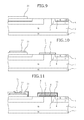
- FIG. 1 is a cross-sectional view of a MOSFET in a first embodiment of a semiconductor device of the present invention
- FIGS. 2, 3, 4, 5, and 6 are cross-sectional view of the MOSFET in the first embodiment of the semiconductor device of the present invention during manufacture
- FIG. 7 is a cross-sectional view of the MOSFET in a second embodiment of the semiconductor device of the present invention.
- FIGS. 8, 9, 10, 11, and 12 are cross-sectional views of the MOSFET in the second embodiment during manufacture.
- FIG. 13 is a cross-sectional view of a conventional MOSFET.
- FIG. 1 is a cross-sectional view of a MOSFET in a first embodiment of the semiconductor device of the present invention.
- a first conductivity type is assumed to be an N-type and a second conductivity type is assumed to be a P-type, these types may be formed inversely.
- An N-type SiC layer 2 having a low impurity concentration is formed on a front surface side of an N-type SiC substrate 1 and plural P-type regions 3 are formed in a surface layer of the N-type SiC layer 2 .
- An N-type source region 4 and a P-type contact region 5 of a high impurity concentration are further formed in a surface layer of the P-type regions 3 .
- a gate insulating film 6 is formed on a region from the N-type source region 4 through the P-type region 3 to the N-type SiC layer 2 , and a first gate electrode 7 is formed by polysilicon on the gate insulating film 6 .
- An interlayer insulating film 8 is formed to cover the first gate electrode 7 and a first barrier film 10 of layered titanium nitride (TiN) or, titanium (Ti) and TiN is formed so as to cover the interlayer insulating film 8 .
- a first source electrode 9 is formed of a nickel silicide on a surface of the N-type source region 4 and the P-type contact region 5 .
- a second source electrode 11 of layered metals such as Ti and aluminum (Al), etc. is formed on the first barrier film 10 and the first source electrode 9 .
- a drain electrode 12 is formed on a back surface side of the N-type SiC substrate 1 .
- a second gate electrode 22 is formed of polysilicon on the oxide film 21 ; a gate pad formed by a second barrier film 31 formed of TiN, or Ti and TiN layered on the second gate electrode 22 and the second gate metal electrode 23 formed by metal such as Ti and Al, etc.; and a gate runner that is a metal layer for connecting the gate electrodes and a gate pad are formed.
- the second gate electrode 22 and the first gate electrode 7 are connected, and when voltage is applied to the second gate metal electrode 23 , the same voltage is further applied to the first gate electrode 7 .
- the first barrier film 10 prevents penetration of Ni during sintering and further prevents short-circuit failures between the gate and source of the device.
- the second barrier film 31 covers a gate contact hole, suppresses reaction with the polysilicon of the first gate electrode 7 , and stabilizes improvement of gate contact resistance and manufacturing processes.
- a source contact portion has a layered structure of Ti and Al of the second source electrode 11 in a nickel silicide layer of the first source electrode 9 .
- a layered structure of Al and Ti of the second source electrode 11 is formed on Ti/TiN or Ti of the first barrier film 10 .
- FIGS. 2, 3, 4, 5, and 6 are cross-sectional view of the MOSFET in the first embodiment of the semiconductor device of the present invention during manufacture. Manufacture of the MOSFET is performed sequentially from (a) to (f).
- the oxide film 21 forming a gate pad, gate runner, etc. is formed to have a thickness of 0.5 ⁇ m or greater.
- the gate insulating film 6 is formed on a region from the N-type source region 4 , through the P-type region 3 to the N-type SiC layer 2 , by an oxide film having a thickness of about 0.1 ⁇ m.
- the first gate electrode 7 is formed of polysilicon to have a thickness of 0.3 ⁇ m or greater and on the oxide film 21 , the second gate electrode 22 is formed.
- the interlayer insulating film 8 is formed of an oxide film of a thickness of 0.5 ⁇ m or greater, and a source and gate contact hole are formed.
- the first barrier film 10 is formed by a layered film of Ti/TiN or a single-layer film of TiN of a thickness of about 0.1 ⁇ m so as to cover the interlayer insulating film 8 and the second barrier film 31 is formed at the gate contact portion as well.
- the first source electrode 9 is formed by Ni of a thickness of about 0.05 ⁇ m.
- a sintering process at a temperature of 800 to 1200 degrees C. is performed and, the second source electrode 11 and the second gate metal electrode 23 are formed by a layered film of Ti and metal (Al, etc.) to have a thickness of 2.0 ⁇ m or greater.
- the drain electrode 12 is formed, whereby the MOSFET device structure depicted in FIG. 1 is obtained.
- TiN used in the first barrier film 10 and the second barrier film 31 is susceptible to corrosion by rest potential and therefore, the surface has to be covered by metal.
- metal although use of a single-layer film such as Al is effective, if gaps form in between with the TiN consequent to insufficient coverage, corrosion occurs consequent to oxidation of these gaps. To prevent this and ensure stable quality and reliability, the surface has to be cover with Ti. Although this Ti formation may be performed separately, the number of processes increases. Therefore, at process (f) above, at the time of formation of the second source electrode 11 and the second gate metal electrode 23 , formation as layered metal electrodes using Ti enables the top of the TiN to be covered by Ti without increasing the number of processes.
- FIG. 7 is a cross-sectional view of the MOSFET in a second embodiment of the semiconductor device of the present invention.
- the second embodiment differs from the first embodiment in that a third barrier film 32 is further formed on the first source electrode 9 .
- This is applicable when the Ni of the first source electrode 9 is formed in the source-contact layer without contacting the interlayer insulating film 8 and there is no penetration of Ni during sintering and enables suppression of cracking of TiN consequent to the stress from the formation of the third barrier film 32 at the source contact portion and improved reliability of the element.
- FIGS. 8, 9, 10, 11, and 12 are cross-sectional views of the MOSFET in the second embodiment during manufacture. Manufacture of the MOSFET is performed sequentially from (a) to (f).
- the oxide film 21 forming a gate pad, gate runner, etc. is formed to have a thickness of 0.5 ⁇ m or greater.
- the gate insulating film 6 is formed on a region from the N-type source region 4 , through the P-type region 3 to the N-type SiC layer 2 , by an oxide film having a thickness of about 0.1 ⁇ m.
- the first gate electrode 7 is formed of polysilicon to have a thickness of 0.3 ⁇ m or greater and on the oxide film 21 , the second gate electrode 22 is formed.
- the interlayer insulating film 8 is formed of an oxide film of a thickness of 0.5 ⁇ m or greater, and a source and gate contact hole are formed.
- the first barrier film 10 is formed by a layered film of Ti/TiN or a single-layer film of TiN of a thickness of about 0.1 ⁇ m so as to cover the interlayer insulating film 8 and the second barrier film 31 is formed at the gate contact portion as well.
- the first source electrode 9 is formed by Ni to have a thickness of about 0.05 ⁇ m.
- the third barrier film 32 is further formed by a layered film of Ti/TiN or a single-layer film of TiN of a thickness of about 0.1 ⁇ m.
- a sintering process at a temperature of 800 to 1200 degrees C. is performed and, the second source electrode 11 and the second gate metal electrode 23 are formed by a layered film of Ti and metal (Al, etc.) to have a thickness of 2.0 ⁇ m or greater.
- the drain electrode 12 is formed, whereby the MOSFET device structure depicted in FIG. 7 is obtained.
- the gate contact hole is covered by a barrier film formed by a layered structure of TiN, or Ti and TiN, etc., whereby reaction with the polysilicon of the gate electrode is suppressed, enabling improved gate contact resistance and manufacturing process stabilization.
- the metal used in the electrodes is susceptible to corrosion consequent to the effects of electric potential and humidity during operation of the MOSFET. Corrosion occurs easily in the sequence of TiN>Ti>Al, Al—Si. Thus, TiN surfaces, which are most susceptible to corrosion, are covered by Ti, whereby corrosion of TiN is prevented and, stabilization of contact resistance and MOSFET characteristics, and reliability may be improved.
- a barrier film suppresses Ni penetration into the interlayer insulating film during sintering and even when Ni residue is present, unfavorable occurrences such as decrease of the dielectric breakdown voltage and short circuit between the gate and source are suppressed, enabling stabilization of characteristics and improved reliability.
- gate-contact formation and source-contact formation may be performed concurrently, and gate-contact improvement and process stabilization becomes possible.
- covering the TiN of the barrier film with Ti enables corrosion of the TiN to be prevented and ensures stabilized quality and reliability.
- the invention is not limited to a vertical MOSFET and is similarly applicable to a MOSFET having a trench structure.
- the first source electrode 9 is formed of a nickel (Ni) silicide to reduce the contact resistance.
- Ni nickel
- the first source electrode 9 is formed of a nickel (Ni) silicide to reduce the contact resistance.
- the polysilicon surface reacts with gases in the atmosphere, degrades and enters a similar fragile state. In this manner, when the polysilicon surface degrades, the gate contact becomes insufficient. Further, when Ni residue is present on the interlayer insulating film 8 , the Ni penetrates inside the interlayer insulating film 8 during sintering, short circuit between the gate and source occurs, and dielectric breakdown voltage decreases.
- the gate contact may be formed concurrently with the source contact and improved gate contact and process stabilization becomes possible. Further, covering the TiN of the barrier film with Ti enables corrosion of the TiN to be prevented and ensures stabilized quality and reliability.
- the gate contact may be improved.
- the semiconductor device and the method of manufacturing a semiconductor device according to the present invention are useful for high-voltage semiconductors used in used in power converting equipment, and power supply devices such as in various industrial machines.
Landscapes
- Engineering & Computer Science (AREA)
- Microelectronics & Electronic Packaging (AREA)
- Power Engineering (AREA)
- Condensed Matter Physics & Semiconductors (AREA)
- General Physics & Mathematics (AREA)
- Physics & Mathematics (AREA)
- Computer Hardware Design (AREA)
- Ceramic Engineering (AREA)
- Manufacturing & Machinery (AREA)
- Chemical & Material Sciences (AREA)
- Crystallography & Structural Chemistry (AREA)
- Materials Engineering (AREA)
- Composite Materials (AREA)
- Electrodes Of Semiconductors (AREA)
Abstract
Description
Claims (3)
Priority Applications (1)
| Application Number | Priority Date | Filing Date | Title |
|---|---|---|---|
| US16/521,623 US10692979B2 (en) | 2014-09-08 | 2019-07-25 | Method of manufacturing semiconductor device |
Applications Claiming Priority (3)
| Application Number | Priority Date | Filing Date | Title |
|---|---|---|---|
| JP2014-182769 | 2014-09-08 | ||
| JP2014182769 | 2014-09-08 | ||
| PCT/JP2015/072911 WO2016039073A1 (en) | 2014-09-08 | 2015-08-13 | Semiconductor device and semiconductor device manufacturing method |
Related Parent Applications (1)
| Application Number | Title | Priority Date | Filing Date |
|---|---|---|---|
| PCT/JP2015/072911 Continuation WO2016039073A1 (en) | 2014-09-08 | 2015-08-13 | Semiconductor device and semiconductor device manufacturing method |
Related Child Applications (1)
| Application Number | Title | Priority Date | Filing Date |
|---|---|---|---|
| US16/521,623 Division US10692979B2 (en) | 2014-09-08 | 2019-07-25 | Method of manufacturing semiconductor device |
Publications (2)
| Publication Number | Publication Date |
|---|---|
| US20170025502A1 US20170025502A1 (en) | 2017-01-26 |
| US10396161B2 true US10396161B2 (en) | 2019-08-27 |
Family
ID=55458831
Family Applications (2)
| Application Number | Title | Priority Date | Filing Date |
|---|---|---|---|
| US15/283,950 Active US10396161B2 (en) | 2014-09-08 | 2016-10-03 | Semiconductor device and method of manufacturing semiconductor device |
| US16/521,623 Active US10692979B2 (en) | 2014-09-08 | 2019-07-25 | Method of manufacturing semiconductor device |
Family Applications After (1)
| Application Number | Title | Priority Date | Filing Date |
|---|---|---|---|
| US16/521,623 Active US10692979B2 (en) | 2014-09-08 | 2019-07-25 | Method of manufacturing semiconductor device |
Country Status (3)
| Country | Link |
|---|---|
| US (2) | US10396161B2 (en) |
| JP (1) | JP6260711B2 (en) |
| WO (1) | WO2016039073A1 (en) |
Families Citing this family (1)
| Publication number | Priority date | Publication date | Assignee | Title |
|---|---|---|---|---|
| JP6705231B2 (en) * | 2016-03-16 | 2020-06-03 | 富士電機株式会社 | Silicon carbide semiconductor device and method for manufacturing silicon carbide semiconductor device |
Citations (12)
| Publication number | Priority date | Publication date | Assignee | Title |
|---|---|---|---|---|
| JPS56164573A (en) | 1980-04-17 | 1981-12-17 | Post Office | Semiconductor device and method of producing same |
| US6821886B1 (en) * | 2003-09-05 | 2004-11-23 | Chartered Semiconductor Manufacturing Ltd. | IMP TiN barrier metal process |
| WO2009093602A1 (en) | 2008-01-21 | 2009-07-30 | Nec Lcd Technologies, Ltd. | Display device |
| US20100140697A1 (en) * | 2008-12-08 | 2010-06-10 | Yedinak Joseph A | Trench-Based Power Semiconductor Devices with Increased Breakdown Voltage Characteristics |
| US20110233666A1 (en) * | 2010-03-24 | 2011-09-29 | Alpha And Omega Semiconductor Incorporated | Oxide terminated trench mosfet with three or four masks |
| WO2011125274A1 (en) | 2010-04-06 | 2011-10-13 | 三菱電機株式会社 | Power semiconductor device and method for manufacturing same |
| WO2012032735A1 (en) | 2010-09-06 | 2012-03-15 | パナソニック株式会社 | Semiconductor device and process for production thereof |
| US20120132912A1 (en) | 2010-11-25 | 2012-05-31 | Mitsubishi Electric Corporation | Semiconductor device |
| WO2012086099A1 (en) | 2010-12-21 | 2012-06-28 | 三菱電機株式会社 | Silicon carbide semiconductor device and method for manufacturing same |
| JP2012160485A (en) | 2009-06-09 | 2012-08-23 | Panasonic Corp | Semiconductor device and manufacturing method of the same |
| US20130062624A1 (en) * | 2011-09-08 | 2013-03-14 | Kabushiki Kaisha Toshiba | Semiconductor device and method for manufacturing the same |
| US20140299887A1 (en) * | 2013-04-04 | 2014-10-09 | Monolith Semiconductor, Inc. | Semiconductor devices comprising getter layers and methods of making and using the same |
Family Cites Families (3)
| Publication number | Priority date | Publication date | Assignee | Title |
|---|---|---|---|---|
| JPH0864802A (en) * | 1994-06-07 | 1996-03-08 | Mitsubishi Materials Corp | Silicon carbide semiconductor device and its manufacture |
| JP5860580B2 (en) * | 2009-05-25 | 2016-02-16 | 日産自動車株式会社 | Semiconductor device and manufacturing method thereof |
| JP5997426B2 (en) * | 2011-08-19 | 2016-09-28 | 株式会社日立製作所 | Semiconductor device and manufacturing method of semiconductor device |
-
2015
- 2015-08-13 JP JP2016547790A patent/JP6260711B2/en active Active
- 2015-08-13 WO PCT/JP2015/072911 patent/WO2016039073A1/en active Application Filing
-
2016
- 2016-10-03 US US15/283,950 patent/US10396161B2/en active Active
-
2019
- 2019-07-25 US US16/521,623 patent/US10692979B2/en active Active
Patent Citations (19)
| Publication number | Priority date | Publication date | Assignee | Title |
|---|---|---|---|---|
| JPS56164573A (en) | 1980-04-17 | 1981-12-17 | Post Office | Semiconductor device and method of producing same |
| US4417387A (en) | 1980-04-17 | 1983-11-29 | The Post Office | Gold metallization in semiconductor devices |
| US6821886B1 (en) * | 2003-09-05 | 2004-11-23 | Chartered Semiconductor Manufacturing Ltd. | IMP TiN barrier metal process |
| WO2009093602A1 (en) | 2008-01-21 | 2009-07-30 | Nec Lcd Technologies, Ltd. | Display device |
| US20100289997A1 (en) | 2008-01-21 | 2010-11-18 | Nec Corporation | Display device |
| US20100140697A1 (en) * | 2008-12-08 | 2010-06-10 | Yedinak Joseph A | Trench-Based Power Semiconductor Devices with Increased Breakdown Voltage Characteristics |
| JP2012160485A (en) | 2009-06-09 | 2012-08-23 | Panasonic Corp | Semiconductor device and manufacturing method of the same |
| US20110233666A1 (en) * | 2010-03-24 | 2011-09-29 | Alpha And Omega Semiconductor Incorporated | Oxide terminated trench mosfet with three or four masks |
| WO2011125274A1 (en) | 2010-04-06 | 2011-10-13 | 三菱電機株式会社 | Power semiconductor device and method for manufacturing same |
| US20130020587A1 (en) | 2010-04-06 | 2013-01-24 | Mitsubishi Electric Corporation | Power semiconductor device and method for manufacturing same |
| WO2012032735A1 (en) | 2010-09-06 | 2012-03-15 | パナソニック株式会社 | Semiconductor device and process for production thereof |
| US20130082285A1 (en) | 2010-09-06 | 2013-04-04 | Panasonic Corporation | Semiconductor device and process for production thereof |
| US20120132912A1 (en) | 2010-11-25 | 2012-05-31 | Mitsubishi Electric Corporation | Semiconductor device |
| JP2012129503A (en) | 2010-11-25 | 2012-07-05 | Mitsubishi Electric Corp | Semiconductor device |
| WO2012086099A1 (en) | 2010-12-21 | 2012-06-28 | 三菱電機株式会社 | Silicon carbide semiconductor device and method for manufacturing same |
| US20140001472A1 (en) | 2010-12-21 | 2014-01-02 | Mitsubishi Electric Corporation | Silicon carbide semiconductor device and method of fabricating same |
| US20130062624A1 (en) * | 2011-09-08 | 2013-03-14 | Kabushiki Kaisha Toshiba | Semiconductor device and method for manufacturing the same |
| JP2013058603A (en) | 2011-09-08 | 2013-03-28 | Toshiba Corp | Semiconductor device and method of manufacturing semiconductor device |
| US20140299887A1 (en) * | 2013-04-04 | 2014-10-09 | Monolith Semiconductor, Inc. | Semiconductor devices comprising getter layers and methods of making and using the same |
Also Published As
| Publication number | Publication date |
|---|---|
| JPWO2016039073A1 (en) | 2017-04-27 |
| WO2016039073A1 (en) | 2016-03-17 |
| US20190348502A1 (en) | 2019-11-14 |
| US20170025502A1 (en) | 2017-01-26 |
| US10692979B2 (en) | 2020-06-23 |
| JP6260711B2 (en) | 2018-01-17 |
Similar Documents
| Publication | Publication Date | Title |
|---|---|---|
| KR101642753B1 (en) | Semiconductor device | |
| US8314447B2 (en) | Semiconductor including lateral HEMT | |
| CN109075089B (en) | Power semiconductor device and method for manufacturing the same | |
| US10204990B2 (en) | Semiconductor device and method of manufacturing semiconductor device | |
| US9837530B2 (en) | Semiconductor device and method of manufacturing the same | |
| US10236339B2 (en) | Semiconductor device | |
| JP2011071307A (en) | Field effect transistor and method of manufacturing the same | |
| US20160260810A1 (en) | Semiconductor device | |
| US10692979B2 (en) | Method of manufacturing semiconductor device | |
| CN107017288B (en) | Semiconductor device and method for manufacturing semiconductor device | |
| JP6552925B2 (en) | Semiconductor device | |
| US20200083367A1 (en) | Semiconductor device | |
| US10032894B2 (en) | Silicon carbide semiconductor device and method of manufacturing silicon carbide semiconductor device | |
| JP2019071312A (en) | Semiconductor device | |
| US10916635B2 (en) | Semiconductor device | |
| JP6782213B2 (en) | Semiconductor device | |
| US20230299150A1 (en) | Semiconductor device | |
| CN106981508B (en) | Horizontal semiconductor element with vertical type bridging structure electrode | |
| US20180286955A1 (en) | Semiconductor device |
Legal Events
| Date | Code | Title | Description |
|---|---|---|---|
| AS | Assignment |
Owner name: FUJI ELECTRIC CO., LTD., JAPAN Free format text: ASSIGNMENT OF ASSIGNORS INTEREST;ASSIGNORS:HARADA, YUICHI;HOSHI, YASUYUKI;KINOSHITA, AKIMASA;AND OTHERS;REEL/FRAME:039924/0196 Effective date: 20160822 |
|
| STPP | Information on status: patent application and granting procedure in general |
Free format text: DOCKETED NEW CASE - READY FOR EXAMINATION |
|
| STPP | Information on status: patent application and granting procedure in general |
Free format text: NOTICE OF ALLOWANCE MAILED -- APPLICATION RECEIVED IN OFFICE OF PUBLICATIONS |
|
| STPP | Information on status: patent application and granting procedure in general |
Free format text: PUBLICATIONS -- ISSUE FEE PAYMENT VERIFIED |
|
| STCF | Information on status: patent grant |
Free format text: PATENTED CASE |
|
| MAFP | Maintenance fee payment |
Free format text: PAYMENT OF MAINTENANCE FEE, 4TH YEAR, LARGE ENTITY (ORIGINAL EVENT CODE: M1551); ENTITY STATUS OF PATENT OWNER: LARGE ENTITY Year of fee payment: 4 |