US10380395B2 - Optical sensor with angled reflectors - Google Patents
Optical sensor with angled reflectors Download PDFInfo
- Publication number
- US10380395B2 US10380395B2 US15/283,007 US201615283007A US10380395B2 US 10380395 B2 US10380395 B2 US 10380395B2 US 201615283007 A US201615283007 A US 201615283007A US 10380395 B2 US10380395 B2 US 10380395B2
- Authority
- US
- United States
- Prior art keywords
- light
- display
- reflective
- reflective surface
- reflective surfaces
- Prior art date
- Legal status (The legal status is an assumption and is not a legal conclusion. Google has not performed a legal analysis and makes no representation as to the accuracy of the status listed.)
- Active, expires
Links
- 230000003287 optical effect Effects 0.000 title claims abstract description 47
- 238000003384 imaging method Methods 0.000 claims description 28
- 239000000463 material Substances 0.000 claims description 18
- 230000000903 blocking effect Effects 0.000 claims description 7
- 238000000034 method Methods 0.000 abstract description 14
- 238000012634 optical imaging Methods 0.000 abstract description 4
- 239000010410 layer Substances 0.000 description 59
- 238000012545 processing Methods 0.000 description 39
- 239000000758 substrate Substances 0.000 description 11
- 238000001465 metallisation Methods 0.000 description 10
- 239000004973 liquid crystal related substance Substances 0.000 description 9
- 239000011521 glass Substances 0.000 description 8
- 230000006870 function Effects 0.000 description 7
- 239000010409 thin film Substances 0.000 description 6
- 239000012780 transparent material Substances 0.000 description 6
- 230000005540 biological transmission Effects 0.000 description 5
- 239000006059 cover glass Substances 0.000 description 5
- 238000005286 illumination Methods 0.000 description 5
- 230000008569 process Effects 0.000 description 5
- 238000010586 diagram Methods 0.000 description 4
- 238000005516 engineering process Methods 0.000 description 4
- 238000003491 array Methods 0.000 description 3
- 238000004891 communication Methods 0.000 description 3
- 230000000007 visual effect Effects 0.000 description 3
- VYPSYNLAJGMNEJ-UHFFFAOYSA-N Silicium dioxide Chemical compound O=[Si]=O VYPSYNLAJGMNEJ-UHFFFAOYSA-N 0.000 description 2
- 230000015572 biosynthetic process Effects 0.000 description 2
- 239000011248 coating agent Substances 0.000 description 2
- 238000000576 coating method Methods 0.000 description 2
- 238000013461 design Methods 0.000 description 2
- 230000000694 effects Effects 0.000 description 2
- 238000005401 electroluminescence Methods 0.000 description 2
- 238000001914 filtration Methods 0.000 description 2
- 239000010931 gold Substances 0.000 description 2
- 238000004519 manufacturing process Methods 0.000 description 2
- 239000011159 matrix material Substances 0.000 description 2
- 229910052751 metal Inorganic materials 0.000 description 2
- 239000002184 metal Substances 0.000 description 2
- 230000002093 peripheral effect Effects 0.000 description 2
- 239000004033 plastic Substances 0.000 description 2
- 230000002792 vascular Effects 0.000 description 2
- 210000003462 vein Anatomy 0.000 description 2
- 241000699670 Mus sp. Species 0.000 description 1
- BQCADISMDOOEFD-UHFFFAOYSA-N Silver Chemical compound [Ag] BQCADISMDOOEFD-UHFFFAOYSA-N 0.000 description 1
- 239000011358 absorbing material Substances 0.000 description 1
- 229910052782 aluminium Inorganic materials 0.000 description 1
- XAGFODPZIPBFFR-UHFFFAOYSA-N aluminium Chemical compound [Al] XAGFODPZIPBFFR-UHFFFAOYSA-N 0.000 description 1
- 229910021417 amorphous silicon Inorganic materials 0.000 description 1
- 210000004204 blood vessel Anatomy 0.000 description 1
- 230000001413 cellular effect Effects 0.000 description 1
- 230000008859 change Effects 0.000 description 1
- 229910052681 coesite Inorganic materials 0.000 description 1
- 239000003086 colorant Substances 0.000 description 1
- 239000002131 composite material Substances 0.000 description 1
- 230000003750 conditioning effect Effects 0.000 description 1
- 239000000356 contaminant Substances 0.000 description 1
- 229910052906 cristobalite Inorganic materials 0.000 description 1
- 230000001419 dependent effect Effects 0.000 description 1
- 238000000151 deposition Methods 0.000 description 1
- 238000001312 dry etching Methods 0.000 description 1
- 238000009713 electroplating Methods 0.000 description 1
- 238000005538 encapsulation Methods 0.000 description 1
- 239000003822 epoxy resin Substances 0.000 description 1
- 238000005242 forging Methods 0.000 description 1
- PCHJSUWPFVWCPO-UHFFFAOYSA-N gold Chemical compound [Au] PCHJSUWPFVWCPO-UHFFFAOYSA-N 0.000 description 1
- 229910052737 gold Inorganic materials 0.000 description 1
- 229910052809 inorganic oxide Inorganic materials 0.000 description 1
- 230000010354 integration Effects 0.000 description 1
- 230000001788 irregular Effects 0.000 description 1
- 230000007246 mechanism Effects 0.000 description 1
- 239000007769 metal material Substances 0.000 description 1
- 238000012986 modification Methods 0.000 description 1
- 230000004048 modification Effects 0.000 description 1
- 238000000465 moulding Methods 0.000 description 1
- 229910021420 polycrystalline silicon Inorganic materials 0.000 description 1
- 229920000647 polyepoxide Polymers 0.000 description 1
- 229920005591 polysilicon Polymers 0.000 description 1
- 239000011148 porous material Substances 0.000 description 1
- 238000007639 printing Methods 0.000 description 1
- 238000002310 reflectometry Methods 0.000 description 1
- 230000004044 response Effects 0.000 description 1
- 229910052594 sapphire Inorganic materials 0.000 description 1
- 239000010980 sapphire Substances 0.000 description 1
- 239000000377 silicon dioxide Substances 0.000 description 1
- 235000012239 silicon dioxide Nutrition 0.000 description 1
- 229910052709 silver Inorganic materials 0.000 description 1
- 239000004332 silver Substances 0.000 description 1
- 239000002356 single layer Substances 0.000 description 1
- 239000007787 solid Substances 0.000 description 1
- 230000003595 spectral effect Effects 0.000 description 1
- 238000001228 spectrum Methods 0.000 description 1
- 238000004528 spin coating Methods 0.000 description 1
- 238000005507 spraying Methods 0.000 description 1
- 238000004544 sputter deposition Methods 0.000 description 1
- 230000003068 static effect Effects 0.000 description 1
- 229910052682 stishovite Inorganic materials 0.000 description 1
- 210000004243 sweat Anatomy 0.000 description 1
- 230000026676 system process Effects 0.000 description 1
- 229910052905 tridymite Inorganic materials 0.000 description 1
- 238000001039 wet etching Methods 0.000 description 1
Images


Classifications
-
- G06K9/00013—
-
- H—ELECTRICITY
- H01—ELECTRIC ELEMENTS
- H01L—SEMICONDUCTOR DEVICES NOT COVERED BY CLASS H10
- H01L27/00—Devices consisting of a plurality of semiconductor or other solid-state components formed in or on a common substrate
- H01L27/14—Devices consisting of a plurality of semiconductor or other solid-state components formed in or on a common substrate including semiconductor components sensitive to infrared radiation, light, electromagnetic radiation of shorter wavelength or corpuscular radiation and specially adapted either for the conversion of the energy of such radiation into electrical energy or for the control of electrical energy by such radiation
- H01L27/144—Devices controlled by radiation
- H01L27/146—Imager structures
- H01L27/14601—Structural or functional details thereof
- H01L27/14625—Optical elements or arrangements associated with the device
- H01L27/14629—Reflectors
-
- G06K9/0008—
-
- G06K9/22—
-
- G—PHYSICS
- G06—COMPUTING; CALCULATING OR COUNTING
- G06V—IMAGE OR VIDEO RECOGNITION OR UNDERSTANDING
- G06V10/00—Arrangements for image or video recognition or understanding
- G06V10/10—Image acquisition
- G06V10/17—Image acquisition using hand-held instruments
-
- G—PHYSICS
- G06—COMPUTING; CALCULATING OR COUNTING
- G06V—IMAGE OR VIDEO RECOGNITION OR UNDERSTANDING
- G06V40/00—Recognition of biometric, human-related or animal-related patterns in image or video data
- G06V40/10—Human or animal bodies, e.g. vehicle occupants or pedestrians; Body parts, e.g. hands
- G06V40/12—Fingerprints or palmprints
- G06V40/13—Sensors therefor
-
- G—PHYSICS
- G06—COMPUTING; CALCULATING OR COUNTING
- G06V—IMAGE OR VIDEO RECOGNITION OR UNDERSTANDING
- G06V40/00—Recognition of biometric, human-related or animal-related patterns in image or video data
- G06V40/10—Human or animal bodies, e.g. vehicle occupants or pedestrians; Body parts, e.g. hands
- G06V40/12—Fingerprints or palmprints
- G06V40/1347—Preprocessing; Feature extraction
- G06V40/1359—Extracting features related to ridge properties; Determining the fingerprint type, e.g. whorl or loop
-
- H—ELECTRICITY
- H01—ELECTRIC ELEMENTS
- H01L—SEMICONDUCTOR DEVICES NOT COVERED BY CLASS H10
- H01L27/00—Devices consisting of a plurality of semiconductor or other solid-state components formed in or on a common substrate
- H01L27/14—Devices consisting of a plurality of semiconductor or other solid-state components formed in or on a common substrate including semiconductor components sensitive to infrared radiation, light, electromagnetic radiation of shorter wavelength or corpuscular radiation and specially adapted either for the conversion of the energy of such radiation into electrical energy or for the control of electrical energy by such radiation
- H01L27/144—Devices controlled by radiation
- H01L27/146—Imager structures
- H01L27/14683—Processes or apparatus peculiar to the manufacture or treatment of these devices or parts thereof
- H01L27/14685—Process for coatings or optical elements
Definitions
- This disclosure generally relates to optical sensors, and more particularly to an optical sensor having angled reflectors.
- biometric recognition systems image biometric objects for authenticating and/or verifying users of devices incorporating the recognition systems.
- Biometric imaging provides a reliable, non-intrusive way to verify individual identity for recognition purposes.
- Various types of sensors may be used for biometric imaging.
- Fingerprints like various other biometric characteristics, are based on distinctive personal characteristics and thus provide a reliable mechanism to recognize an individual.
- fingerprint sensors have many potential applications.
- fingerprint sensors may be used to provide access control in stationary applications, such as security checkpoints.
- Fingerprint sensors may also be used to provide access control in mobile devices, such as cell phones, wearable smart devices (e.g., smart watches and activity trackers), tablet computers, personal data assistants (PDAs), navigation devices, and portable gaming devices. Accordingly, some applications, in particular applications related to mobile devices, may require recognition systems that are both small in size and highly reliable.
- capacitive fingerprint sensors are based on optical or capacitive sensing technologies. While capacitive fingerprint sensors provide certain advantages, most commercially available capacitive fingerprint sensors have difficulty sensing fine ridge and valley features through large distances, requiring the fingerprint to contact a sensing surface that is close to the sensing array. It remains a significant challenge for a capacitive sensor to detect fingerprints through thick layers, such as the thick cover glass (sometimes referred to herein as a “cover lens”) that protects the display of many smart phones and other mobile devices.
- cover glass sometimes referred to herein as a “cover lens”
- a cutout is often formed in the cover glass in an area beside the display, and a discrete capacitive fingerprint sensor (often integrated with a mechanical button) is placed in the cutout area so that it can detect fingerprints without having to sense through the cover glass.
- a discrete capacitive fingerprint sensor (often integrated with a mechanical button) is placed in the cutout area so that it can detect fingerprints without having to sense through the cover glass.
- a hole in the device enclosure also can allow moisture or contaminants to enter the device.
- the existence of mechanical buttons also takes up valuable device real estate.
- the optical sensor includes a plurality of imaging cells, each imaging cell images a portion of the biometric input object to be imaged.
- Each imaging cell includes a first detector element positioned in a detector plane; a first reflective surface, the first reflective surface positioned to receive light from a first sensing region of the display and to reflect the received light; and a second reflective surface, the second reflective surface positioned to receive the reflected light from the first reflective surface, and to further reflect the light in a path that is substantially normal to the detector plane and towards the first detector element.
- the optical sensor includes a set of detector elements positioned in a detector plane; a transparent layer; a set of first reflective surfaces in the transparent layer, each reflective surface in the first set of reflective surfaces positioned to receive light from a portion of a sensing region of the display and to reflect the received light; and a second set of reflective surfaces, each reflective surface in the second set of reflective surfaces positioned to receive the reflected light from the first set of reflective surfaces, and to further reflect the received light in a path that is substantially normal to the detector plane and towards a detector element in the set of detector elements.
- the method includes forming a first transparent layer from a first transparent material having a first index of refraction; forming an array of voids on a top of the first transparent layer, the voids having angled surfaces; forming a first reflective surface at a first angled surface and a second reflective surface at a second angled surface, wherein the first reflective surface is configured to receive light from above and reflect light towards the second reflective surface, and the second reflective surface is configured to receive the reflected light and to further reflect the light towards a detector element.
- the method further includes forming a second transparent layer from a second transparent material having a second index of refraction; wherein the second transparent material fills the array of voids.
- FIG. 1 is a block diagram of an example of a sensing system.
- FIGS. 2A -2C are schematic diagrams of sensor arrangements for imaging an input object, wherein the detector element detects light from above.
- FIG. 3 is a schematic diagram of a sensor arrangement for imaging an input object, wherein the detector element detects light from below.
- FIGS. 4A-4C illustrate top views of sensor arrangement for imaging an input object.
- FIGS. 5A-5B illustrate a process for making a sensor arrangement.
- embodiments provide systems and methods to optically image an input object such as biometric objects including fingerprints.
- a system and method are described for an in-display optical imaging system including of an array of imaging cells, which include dual-mirror periscope like arrangements.
- the imaging system is suitable for integration of a biometric sensor, such as a fingerprint sensor, with a display, such as for example a liquid crystal display (LCD), light emitting diode (LED) display or organic LED (OLED) display.
- LCD liquid crystal display
- LED light emitting diode
- OLED organic LED
- Each imaging cell including the dual-mirror arrangement, serves as an optical element, which limits the field of view seen by each detector and the area it samples on the biometric, e.g. finger.
- the sensor arrangement may be fabricated as part of the display, for example, on the encapsulating glass (color filter glass in case of LCD) or the active backplane of the display. The arrangement reduces thickness of the optical sensor and minimizes or eliminates interference with display image quality.
- FIG. 1 is a block diagram of an exemplary sensing system having a sensor 100 , in accordance with embodiments of the disclosure.
- the sensor 100 may be configured to provide input to an electronic system (also “electronic device”).
- electronic systems include personal computers of all sizes and shapes, such as desktop computers, laptop computers, netbook computers, tablets, e-book readers, personal digital assistants (PDAs), and wearable computers (such as smart watches and activity tracker devices).
- Additional example electronic systems include composite input devices, such as physical keyboards that include input device 100 and separate joysticks or key switches.
- Further example electronic systems include peripherals such as data input devices (including remote controls and mice), and data output devices (including display screens and printers).
- remote terminals e.g., video game consoles, portable gaming devices, and the like.
- video game machines e.g., video game consoles, portable gaming devices, and the like.
- communication devices including cellular phones, such as smart phones
- media devices including recorders, editors, and players such as televisions, set-top boxes, music players, digital photo frames, and digital cameras.
- the electronic system could be a host or a slave to the input device.
- the sensor 100 can be implemented as a physical part of the electronic system, or can be physically separate from the electronic system. In accordance with the disclosure, the sensor 100 may be integrated as part of a display of an electronic device. As appropriate, the sensor 100 may communicate with parts of the electronic system using any one or more of the following: buses, networks, and other wired or wireless interconnections. Examples include I 2 C, SPI, PS/2, Universal Serial Bus (USB), Bluetooth, RF, and IRDA.
- the sensor 100 is configured to sense input provided by one or more input objects 140 in a sensing region 120 .
- the input object 140 is a finger
- the sensor 100 is implemented as a fingerprint sensor (also “fingerprint scanner”) configured to detect fingerprint features of the input object 140 .
- the sensor 100 may be implemented as vascular sensor (e.g., for finger vein recognition), hand geometry sensor, or a proximity sensor (such as a touch pad, touch screen, and or other touch sensor device).
- Sensing region 120 encompasses any space above, around, in, and/or near the sensor 100 in which the sensor 100 is able to detect input (e.g., user input provided by one or more input objects 140 ).
- the sizes, shapes, and locations of particular sensing regions may vary widely from embodiment to embodiment.
- the sensing region 120 extends from a surface of the sensor 100 in one or more directions into space.
- input surfaces may be provided by surfaces of casings within which sensor elements reside, by face sheets applied over the sensor elements or any casings, etc.
- the sensing region 120 has a rectangular shape when projected onto an input surface of the input device 100 .
- the sensor 100 may utilize any combination of sensor components and sensing technologies to detect user input in the sensing region 120 .
- the sensor 100 comprises one or more detector elements (or “sensing elements”) for detecting user input. Some implementations utilize arrays or other regular or irregular patterns of sensing elements to detect the input object 140 .
- one or more detector elements detect light from the sensing region.
- the detected light may be reflected from input objects in the sensing region, emitted by input objects in the sensing region, or some combination thereof.
- Example optical detector elements include photodiodes, CMOS arrays, CCD arrays, photodiodes, and other types of photosensors configured to detect light in the visible or invisible spectrum (such as infrared or ultraviolet light).
- the photosensors may be thin film photodetectors, such as thin film transistors (TFTs) or thin film diodes.
- Some optical implementations provide illumination to the sensing region. Reflections from the sensing region in the illumination wavelength(s) are detected to determine input information corresponding to the input object.
- Some optical implementations rely on principles of direct illumination of the input object, which may or may not be in contact with an input surface of the sensing region depending on the configuration.
- One or more light sources and/or light guiding structures may be used to direct light to the sensing region. When an input object is present, this light is reflected from surfaces of the input object, which reflections can be detect by the optical sensing elements and used to determine information about the input object.
- Some optical implementations rely on principles of internal reflection to detect input objects in contact with the input surface of the sensing region.
- One or more light sources may be used to direct light in a transmitting medium at an angle at which it is internally reflected at the input surface of the sensing region, due to different refractive indices at opposing sides of the boundary defined by the sensing surface. Contact of the input surface by the input object causes the refractive index to change across this boundary, which alters the internal reflection characteristics at the input surface.
- Higher contrast signals can often be achieved if principles of frustrated total internal reflection (FTIR) are used to detect the input object.
- FTIR frustrated total internal reflection
- the light may be directed to the input surface at an angle of incidence at which it is totally internally reflected, except where the input object is in contact with the input surface and causes the light to partially transmit across this interface.
- An example of this is presence of a finger introduced to an input surface defined by a glass to air interface.
- the higher refractive index of human skin compared to air causes light incident at the input surface at the critical angle of the interface to air to be partially transmitted through the finger, where it would otherwise be totally internally reflected at the glass to air interface.
- This optical response can be detected by the system and used to determine spatial information. In some embodiments, this can be used to image small scale fingerprint features, where the internal reflectivity of the incident light differs depending on whether a ridge or valley is in contact with that portion of the input surface.
- the input device may have a sensor resolution that varies from embodiment to embodiment depending on factors such as the particular sensing technology involved and/or the scale of information of interest.
- some biometric sensing implementations may be configured to detect physiological features of the input object (such as fingerprint ridge features of a finger, or blood vessel patterns of an eye), which may utilize higher sensor resolutions and present different technical considerations from some proximity sensor implementations that are configured to detect a position of the input object with respect to the sensing region (such as a touch position of a finger with respect to an input surface).
- the sensor resolution is determined by the physical arrangement of an array of sensing elements, where smaller sensing elements and/or a smaller pitch can be used to define a higher sensor resolution.
- the sensor 100 is implemented as a fingerprint sensor having a sensor resolution high enough to capture features of a fingerprint.
- the fingerprint sensor has a resolution sufficient to capture minutia (including ridge endings and bifurcations), orientation fields (sometimes referred to as “ridge flows”), and/or ridge skeletons. These are sometimes referred to as level 1 and level 2 features, and in an exemplary embodiment, a resolution of at least 250 pixels per inch (ppi) is capable of reliably capturing these features.
- the fingerprint sensor has a resolution sufficient to capture higher level features, such as sweat pores or edge contours (i.e., shapes of the edges of individual ridges). These are sometimes referred to as level 3 features, and in an exemplary embodiment, a resolution of at least 750 pixels per inch (ppi) is capable of reliably capturing these higher level features.
- the fingerprint sensor is implemented as a placement sensor (also “area” sensor or “static” sensor) or a swipe sensor (also “slide” sensor or “sweep” sensor).
- a placement sensor also “area” sensor or “static” sensor
- a swipe sensor also “slide” sensor or “sweep” sensor.
- the sensor is configured to capture a fingerprint input as the user's finger is held stationary over the sensing region.
- the placement sensor includes a two dimensional array of sensing elements capable of capturing a desired area of the fingerprint in a single frame.
- the sensor is configured to capture to a fingerprint input based on relative movement between the user's finger and the sensing region.
- the swipe sensor includes a linear array or a thin two-dimensional array of sensing elements configured to capture multiple frames as the user's finger is swiped over the sensing region. The multiple frames may then be reconstructed to form an image of the fingerprint corresponding to the fingerprint input.
- the sensor is configured to capture both placement and swipe inputs.
- the fingerprint sensor is configured to capture less than a full area of a user's fingerprint in a single user input (referred to herein as a “partial” fingerprint sensor).
- the resulting partial area of the fingerprint captured by the partial fingerprint sensor is sufficient for the system to perform fingerprint matching from a single user input of the fingerprint (e.g., a single finger placement or a single finger swipe).
- Some example imaging areas for partial placement sensors include an imaging area of 100 mm 2 or less.
- a partial placement sensor has an imaging area in the range of 20-50 mm 2 .
- the partial fingerprint sensor has an input surface that is the same size as the imaging area.
- a biometric sensor device may be configured to capture physiological biometric characteristics of a user.
- physiological biometric characteristics include fingerprint patterns, vascular patterns (sometimes known as “vein patterns”), palm prints, and hand geometry.
- a processing system 110 is shown in communication with the input device 100 .
- the processing system 110 comprises parts of or all of one or more integrated circuits (ICs) including microprocessors, microcontrollers and the like and/or other circuitry components.
- ICs integrated circuits
- the processing system may be configured to operate hardware of the input device to capture input data, and/or implement a biometric process or other process based on input data captured by the sensor 100 .
- the processing system 110 is configured to operate sensor hardware of the sensor 100 to detect input in the sensing region 120 .
- the processing system comprises driver circuitry configured to drive signals with sensing hardware of the input device and/or receiver circuitry configured to receive signals with the sensing hardware.
- a processing system for an optical sensor device may comprise driver circuitry configured to drive illumination signals to one or more LEDs, an LCD backlight or other light sources, and/or receiver circuitry configured to receive signals with optical receiving elements.
- the processing system 110 comprises electronically-readable instructions, such as firmware code, software code, and/or the like.
- the processing system 110 includes memory for storing electronically-readable instructions and/or other data, such as reference templates for biometric recognition.
- the processing system 110 can be implemented as a physical part of the sensor 100 , or can be physically separate from the sensor 100 .
- the processing system 110 may communicate with parts of the sensor 100 using buses, networks, and/or other wired or wireless interconnections.
- components composing the processing system 110 are located together, such as near sensing element(s) of the sensor 100 .
- components of processing system 110 are physically separate with one or more components close to sensing element(s) of sensor 100 , and one or more components elsewhere.
- the senor 100 may be a peripheral coupled to a computing device, and the processing system 110 may comprise software configured to run on a central processing unit of the computing device and one or more ICs (perhaps with associated firmware) separate from the central processing unit.
- the sensor 100 may be physically integrated in a mobile device, and the processing system 110 may comprise circuits and/or firmware that are part of a central processing unit or other main processor of the mobile device.
- the processing system 110 is dedicated to implementing the sensor 100 .
- the processing system 110 performs functions associated with the sensor and also performs other functions, such as operating display screens, driving haptic actuators, running an operating system (OS) for the electronic system, etc.
- OS operating system
- the processing system 110 may be implemented as a set of modules that handle different functions of the processing system 110 .
- Each module may comprise circuitry that is a part of the processing system 110 , firmware, software, or a combination thereof.
- Example modules include hardware operation modules for operating hardware such as sensor electrodes and display screens, data processing modules for processing data such as sensor signals and positional information, and reporting modules for reporting information.
- Further example modules include sensor operation modules configured to operate sensing element(s) to detect input, identification modules configured to identify gestures such as mode changing gestures, and mode changing modules for changing operation modes.
- a first and second module may be comprised in separate integrated circuits.
- a first module may be comprised at least partially within a first integrated circuit and a separate module may be comprised at least partially within a second integrated circuit. Further, portions of a single module may span multiple integrated circuits.
- the processing system 110 responds to user input (or lack of user input) in the sensing region 120 directly by causing one or more actions.
- Example actions include unlocking a device or otherwise changing operation modes, as well as GUI actions such as cursor movement, selection, menu navigation, and other functions.
- the processing system 110 provides information about the input (or lack of input) to some part of the electronic system (e.g. to a central processing system of the electronic system that is separate from the processing system 110 , if such a separate central processing system exists).
- some part of the electronic system processes information received from the processing system 110 to act on user input, such as to facilitate a full range of actions, including mode changing actions and GUI actions.
- the processing system 110 operates the sensing element(s) of the sensor 100 to produce electrical signals indicative of input (or lack of input) in the sensing region 120 .
- the processing system 110 may perform any appropriate amount of processing on the electrical signals in producing the information provided to the electronic system.
- the processing system 110 may digitize analog electrical signals obtained from the sensor electrodes.
- the processing system 110 may perform filtering or other signal conditioning.
- the processing system 110 may subtract or otherwise account for a baseline, such that the information reflects a difference between the electrical signals and the baseline.
- the processing system 110 may determine positional information, recognize inputs as commands, authenticate a user, and the like.
- the sensing region 120 of the sensor 100 overlaps at least part of an active area of a display screen, such as embodiments where the sensor 100 comprises a touch screen interface and/or biometric sensing embodiments configured to detect biometric input data over the active display area.
- the sensor 100 may comprise substantially transparent sensor electrodes.
- the display screen may be any type of dynamic display capable of displaying a visual interface to a user, and may include any type of light emitting diode (LED), organic LED (OLED), cathode ray tube (CRT), liquid crystal display (LCD), plasma, electroluminescence (EL), or other display technology.
- the display screen may also be flexible or rigid, and may be flat, curved, or have other geometries.
- the display screen includes a glass or plastic substrate for TFT circuitry and/or other circuitry, which may be used to provide visuals and/or provide other functionality.
- the display device includes a cover lens (sometimes referred to as a “cover glass”) disposed above display circuitry which may also provide an input surface for the input device.
- cover lens materials include plastic, optically clear amorphous solids, such as chemically hardened glass, as well as optically clear crystalline structures, such as sapphire.
- the sensor 100 and the display screen may share physical elements. For example, some embodiments may utilize some of the same electrical components for displaying visuals and for input sensing.
- one or more display electrodes of a display device may configured for both display updating and input sensing.
- the display screen may be operated in part or in total by the processing system 110 in communication with the input device.
- FIG. 2A illustrates an example of an arrangement for an optical sensor device 200 integrated in a display according to certain embodiments.
- the display is an LCD display; although as will be apparent from the descriptions that follows, the sensor device 200 may be integrated with other types of displays, such as LED and OLED displays.
- the sensor 200 includes detector elements 202 mounted on a bottom substrate 204 forming a detector plane, a liquid crystal layer 206 , a reflective layer 208 , a top substrate 210 and a cover layer 212 .
- the sensor 200 also includes various display elements, which in the context of the LCD display include color filters 214 used to present varying colors, liquid crystals within liquid crystal layer 206 , TFTs 234 , which are collectively used to output an electronic graphical display visible to a user.
- an input object 216 which is any object to be imaged (e.g., fingerprint). It will be appreciated that the components and layers shown are for purposes of illustration only and may vary depending on the particular display into which the sensor arrangement is integrated.
- the cover layer 212 (e.g., cover lens or cover glass) is provided as part of the display to protect inner components of the sensor 200 such as the detector elements 202 , the display elements (e.g. 214 , 234 ) and active backplane.
- a top surface 218 of the cover layer 212 forms a sensing surface, which provides a contact area for the input object 216 . It will be understood that the sensing surface 218 forms part of a sensing region in which an object may be imaged. As previously described, the sensing region may extend above the actual sensing surface 218 .
- the cover layer 212 is shown as a single layer.
- the cover layer 212 may include multiple layers and/or may be combined with the top substrate 210 .
- the cover layer 212 and top substrate 210 may be made from any suitable material, typically a transparent material.
- the input object 216 is any object to be imaged.
- the object 216 will have various features.
- the object 216 has ridges 220 and valleys 222 . Due to their protruding nature, the ridges 220 contact the sensing surface 218 .
- the valleys 222 do not contact the sensing surface 218 and instead form an air gap between the input object 216 and the sensing surface 218 .
- Such features may be optically imaged using direct illumination or by relying on principles of total internal reflection (TIR).
- the detector elements 202 are disposed on or near the bottom substrate 204 and may be any suitable type of photo detector.
- the detector elements 202 may be made from amorphous silicon or polysilicon and may be constructed as photoresistors or thin film photodetectors, such as thin film transistors (TFTs) or thin film photodiodes (e.g. pin or pn diodes).
- TFTs thin film transistors
- TFTs thin film photodiodes
- the display elements include various color filters 214 (e.g., red, green, blue), which may be positioned in the reflective layer 208 , or which may be in a separate layer.
- the color filers 214 are used in conjunction with the liquid crystal layer 206 , backlight 242 , TFT's 234 and associated circuitry to render the display to a user in a manner known to those skilled in the art.
- the TFT's 234 and associated circuitry may be located on the bottom substrate 204 .
- a light source 224 is used as the light source for optical imaging.
- the light source 224 transmits light to the sensing surface 218 , which is then reflected and detected by the detector elements 202 as described further below.
- a separate light source need not be used.
- light 244 from the LCD backlight 242 may be used for the optical imaging.
- the reflective layer 208 is positioned below the top substrate 210 and above the liquid crystal layer 206 .
- the reflective layer 208 includes an array of imaging cells including dual-mirrors, which form periscope type arrangements for directing light reflected from the input object to detector elements.
- the reflective layer 208 is generally made of any transparent material (e.g., glass, epoxy resin such as SU 8 and the like).
- Each imaging cell includes a first reflective surface 226 and a second reflective surface 228 .
- the reflective surfaces 226 and 228 are configured to reflect light and may be constructed, for example, as mirrored surfaces. Although shown as flat surfaces, the reflective surfaces may be curved in a concave or convex arrangement to direct the light as desired. In an alternative arrangement, mirrored surfaces need not be used.
- first reflective surfaces 226 and second reflective surface 228 may be formed as boundaries between areas having differing indices of refraction, which boundaries provide for total internal reflection to direct light along a path as described below.
- a blocking layer having masked surfaces 230 may be disposed toward the top of, or above, the reflective layer 208 .
- the masked surfaces 230 form apertures 232 above at least the first reflective surface 226 .
- the apertures 232 are configured to permit the transmission of certain light reflected from the sensing surface 218 into portions of the reflective layer 208 so as to reach the first reflective surface 226 .
- the masked surfaces 230 may be constructed of a light absorbing material, reflecting material or other material that occludes light from passing through areas other than through defined apertures, e.g. apertures 232 , thereby preventing or limiting unwanted stray light from reaching the detector elements 202 .
- the masked surfaces 230 may also generally be disposed above the second reflective surface 228 .
- the detector elements 202 detect light, which is reflected at sensing surface 218 and/or the input object 216 , through the apertures 232 , which light is first reflected off first reflective surface 226 towards the second reflective surface 228 . The light is received by the second reflective surface 228 and further reflected towards the detector element 202 . The detector element 202 receives and detects the light. Thus, as shown in the embodiment of FIG. 2A , the detector element 202 detects light from above.
- Light reaching a given detector element 202 is generally restricted to an acceptance cone 236 , having an acceptance angle ⁇ to prevent blurring of the image of the input object 216 .
- acceptance cone 236 corresponds to detector element 202 .
- the acceptance cone 236 may, for example, be limited to a few degrees.
- the acceptance angle ⁇ determines the degree of image blurring and the maximum distance from the detector elements 202 that the input object 216 can be located while still achieving a given image resolution.
- the acceptance angle ⁇ is dependent upon a width of the aperture 232 , width of reflective surfaces 226 and 228 , and/or the distance between the reflective surfaces 226 and 228 .
- a photo-detector surface area of the detector element 202 may also be used to control the acceptance angle.
- light ray 238 An example of light falling within the acceptance cone 236 is illustrated by light ray 238 .
- light ray 238 is transmitted from a surface of input object 216 , through aperture 232 to the first reflective surface 226 , where the light is reflected towards the second reflective surface 228 in a path that is substantially or generally parallel to the detector plane relative to the orientation shown.
- the light is then further reflected by the second reflective surface 228 towards the detector element 202 in a path that is substantially or generally normal to the detector plane relative to the orientation shown.
- the light is then received and detected by the detector element 202 .
- light ray 240 which falls at least partially outside of the acceptance cone 236 , is blocked by other portions of the display such as the masked surface 230 .
- the acceptance cone 236 in turn corresponds to a portion of area to be imaged of the input object 216 .
- the sensor 200 will have as many detector elements 202 as needed to image a desired area of the input object 216 and each detector element 202 will have associated apertures (e.g., 232 ) and reflective surfaces 226 , 228 to define an acceptance cone corresponding to an area of the input object 216 to be imaged.
- all detector elements 202 will generally be in the same plane, referred to herein as the detector plane.
- the pitch of detector elements will depend on the resolution desired.
- the processing system 110 may include software and/or hardware which processes individual data obtained via the detector elements, which data may then be stitched together and/or logically combined via a template to form a complete or partial image of an input object (e.g. fingerprint) as desired.
- FIG. 2B illustrates an alternative embodiment of the arrangement of FIG. 2A .
- FIG. 2B depicts the masked surfaces 230 forming aperture 232 and first reflective surface 226 and second reflective surface 228 , which combine to form acceptance cone 236 .
- Light falling within the acceptance cone 236 is directed by the first reflective surface 226 and the second reflective surface 228 to the top surface of detector element 202 in the same manner as described in connection with FIG. 2A .
- the masked surfaces 230 additionally form aperture 250 above the second reflective surface 228 .
- the inclusion of the aperture 250 above reflective surface 228 permits the formation of a second acceptance cone 256 .
- Light transmitted from an area of input object 216 which falls within the acceptance cone 256 enters the reflective layer 208 through aperture 250 , is reflected by the second reflective surface 228 towards a third reflective surface 252 .
- the third reflective surface then receives and reflects the light originating from acceptance cone 256 to a second detector element 254 where the light is received.
- FIG. 2B uses each reflective surface to provide the multiple functions of receiving light from an input object, reflecting the light towards another mirrored surface; and receiving light from yet another mirrored surface and reflecting that light towards a detector element.
- the functions are illustrated by light rays 238 and 262 relative to the reflective surface 228 .
- the arrangement of FIG. 2B may provide for a more compact design compared with the embodiment of FIG. 2A since fewer reflective surfaces are needed to achieve a given resolution.
- the pattern of reflective surfaces and apertures repeats at a pitch as appropriate to provide an imaging area of desired size and resolution.
- FIG. 2C illustrates another embodiment wherein the dual-mirror arrangement is shown integrated in an OLED or LED type display.
- the masked surfaces 230 , apertures 232 , first reflective surface 226 , second reflective surface 228 and detector element 202 are arranged and function as described in connection with FIG. 2A to define the acceptance cone 236 .
- light from within the acceptance cone 236 is guided by the first reflective surface 226 and second reflective surface 228 such that the light reaches detector element 202 as illustrated by light ray 238 .
- Light falling outside of the acceptance cone 236 is generally prevented from reaching the detector elements 202 .
- such light is blocked by masked surfaces 230 as shown by light ray 240 ( FIG. 2A ).
- the liquid crystal layer 206 is not provided and the bottom substrate 204 with detector element 202 may thus be more or less directly below reflective layer 208 .
- the display elements include LEDs or OLEDs 260 on the detector plane, which may be disposed on or near the bottom substrate 204 .
- the LEDs or OLEDs 260 may be in generally the same plane as the detector elements 202 , although it will be understood that positioning of the LEDs or OLEDs in a different plane from the detector elements 202 is also contemplated.
- the LEDs or OLEDs 260 may be used as the light source used to illuminate the input object 216 , although separate light source 224 may be used instead of, or in combination with, the LEDs or OLEDs 260 .
- FIG. 2C can be arranged in accordance with the multi-function reflective surfaces of FIG. 2B .
- the sensor 200 is configured to direct light so that the detector elements 202 detect light from above with the first and second reflective surfaces 226 , 228 being configured appropriately.
- the first and second reflective surfaces 226 , 228 are generally parallel to one another.
- the angle of the reflective surfaces 226 , 228 is about 40-50 degrees from horizontal, although other angles may be used.
- the detector elements 202 are below masked surfaces 230 and reflective surfaces 226 , 228 .
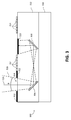
- FIG. 3 illustrates a sensor arrangement 300 that may be used in yet another embodiment.
- the sensor arrangement 300 includes detector elements positioned to detect light from below and the orientation (e.g., angle) of the second reflective surface is adjusted accordingly.
- the arrangement includes reflective layer 302 positioned above a bottom substrate 304 .
- the reflective layer 302 includes first reflective surface 306 and a second reflective surface 308 .
- a detector element 310 is positioned above the second reflective surface 308 .
- Masked surfaces 312 form aperture 314 above the first reflective surface 306 .
- a light shield (not shown) may be provided above the detector element to reduce the possibility of interference by stray light. Typically, the light shield will be close to the detector element 310 , e.g., 1-2 um.
- the shield may comprise metal layers formed when depositing drive or sense electrodes or other parts of TFTs.
- the first reflective surface 306 and the second reflective surface 308 and aperture 314 define an acceptance cone 318 having acceptance angle ⁇ .
- light such as light ray 320 falling within the acceptance cone will reach the bottom of detector element 310 .
- light ray 320 is reflected from the input object (not shown) and is transmitted through aperture 314 .
- the light ray 320 reaches the first reflective surface 306 .
- the light ray 320 is then reflected towards the second reflective surface 308 in a path that is generally or substantially parallel to the detector plane relative to the orientation shown.
- the second reflective surface 308 is configured to then further reflect the light upwards towards the detector element 310 in a path that is generally or substantially normal to the detector plane relative to the orientation shown.
- the detector element 310 then receives the light.
- Light falling outside of the acceptance cone will generally be blocked by other systems components such as masked surfaces 312 .
- the first reflective surface 306 and the second reflective surface 308 are configured to direct light such that the detector element 310 detects light from below.
- the first reflective surface 306 has an angle of about 40-50 degrees from horizontal relative to the orientation shown.
- the second reflective surface 308 is not parallel with the first reflective surface 306 . Instead, the second reflective surface 308 has an angle of about 130 to 140 degree from horizontal relative to the orientation shown.
- the detector element 310 is above the first and second reflective surfaces 308 and 306 .
- FIGS. 4A-4C illustrate examples of a top view of dual-mirrored optical sensors 400 .
- FIGS. 4A-4B more specifically show the placement of the reflective surfaces relative to various display elements and the transmission path of light between the reflective surfaces.
- FIG. 4A shows the reflective surfaces 402 and display elements 404 .
- the display elements 404 may, for example, represent color filters in the case of a LCD display or the LEDs in the case of an OLED or LED display.
- the reflective surfaces 402 are generally positioned between rows the display elements 404 .
- the reflective surfaces 402 are further oriented such that the transmission of light rays 406 between reflective surfaces 402 (e.g. first and second reflective surfaces) follows a path that generally remains between the display elements 404 . In FIG. 4A , the transmission of light rays 406 does not cut across the display elements 404 .
- FIG. 4B also shows reflective surfaces 402 and display elements 404 . Similar to FIG. 4A , the reflective surfaces 402 are generally positioned between rows the display elements 404 . However, in contrast to FIG. 4A , the orientation of reflective surfaces 402 is such that the transmission of light rays 406 between reflective surfaces 402 (first and second reflective surfaces) follows a path that generally cuts across one or more of the display elements 404 . The arrangement of FIG. 4B allows for a more compact design.
- FIG. 4C shows a blocking layer above the reflective surfaces 402 .
- the blocking layer includes masked surfaces 408 , illustrated as shaded areas, and apertures 410 , illustrated as un-shaded areas.
- the masked surfaces 408 occlude light, e.g., absorb light and/or reflect light, while the apertures 410 permit light falling within an acceptance cone to reach at least certain of the reflective surfaces 402 .
- the masked surfaces 408 do not cover the display elements 404 and, therefore, do not inhibit display functionality.
- FIGS. 5A and 5B illustrate a method for making and assembling a reflective layer including the dual-mirror arrangement described herein, which may be integrated in a display.
- steps are described in a particular sequence, the sequence may be altered and/or steps may be combined or eliminated without departing from the scope of the disclosure except where otherwise apparent.
- a first transparent layer 514 having an index of refraction n 1 is formed.
- angled surfaces 516 a , 516 b are formed within the first transparent layer 514 .
- the angled surfaces 516 a , 516 b may be formed, for example, by creating voids in the first transparent layer 514 .
- the voids may have any suitable cross section that provides the angled surfaces, such as for example a trapezoidal or triangular cross section.
- the voids 515 may be formed in a variety of ways including, for example, dry or wet etching, stamping or molding.
- any suitable angle may be selected for the angled surfaces 516 a , 516 b , generally an angle that will allow light to be directed from one finished reflective surface to another (see step 506 ), typically in the range of about 40-50 degrees with 45 degrees being a specific example.
- the angled surfaces 516 a , 516 b are shown as being generally flat, although the angled surfaces may also be curved (concave or convex) so as to further focus and/or direct reflected light.
- a top surface of the first transparent layer 514 is coated with a metallization layer 518 .
- the metallization layer 518 may be added by, for example, sputtering material, electroplating or printing. Examples of materials that can be used for the metallization layer include aluminum (Al), gold (Au) or silver (Ag) to name but a few examples.
- the metallization material may be selected to provide more or less reflection at particular spectral frequencies.
- step 506 portions of the metallization layer 518 are removed, such that metallization only remains on the angled surfaces 516 a , 516 b thereby resulting in a first reflective surface 520 and a second reflective surface 522 .
- the angled surfaces 516 a , 516 b may be treated prior to the metallization step 504 such that metal only adheres to the angled surfaces (e.g., 516 a , 516 b ) during the metallization step thereby obviating the need for removal of metal material.
- a second transparent layer 524 is formed from a second material having an index of refraction n 2 . Formation of the second transparent layer 524 fills the voids 515 formed in the first transparent layer 514 during step 502 .
- the second transparent layer 524 may be added in any suitable manner. Spin coating is one example. Blade coating, slit coating, and spray coating are other examples.
- the top surface of the second transparent layer 524 may be planarized to form a level surface if necessary. It will be appreciated the first transparent layer 514 and second transparent layer 524 may be made from the same type of material or from different types of material.
- a blocking layer 528 with masked surfaces is optionally formed.
- the masked surfaces may be formed of any suitable material, for example a material that occludes light.
- the black matrix may be used for the masked surfaces 528 .
- Openings are formed in the masked surfaces 528 to form apertures 530 through which light may travel.
- the completed assembly forms a reflective layer which allows light to travel from an input object through the periscope structure formed by reflective surfaces 520 and 522 and towards a detector element (not shown).
- An example of light ray traversing the periscope structure is illustrated by light ray 532 . It will be appreciated that only two reflective surfaces are shown and described in FIGS. 5A-5B for purposes of illustration.
- the reflective layer will have a pair of reflective surfaces for each detector element used as part of an overall sensor arrangement consistent with the preceding description.
- the masked surfaces may be omitted where other display components will provide the needed filtering of stray light.
- the particular angled surfaces metalized in step 504 and 506 may be adjusted depending on the configuration. For example, for the arrangement of FIG. 3 , surfaces 516 a and 516 c are metalized instead of surfaces 516 a and 516 b thereby providing an arrangement such as shown and described in connection with FIG. 3 where the detector element receives light from below.
- the reflective surfaces need not be formed by mirrored surfaces formed through metallization. Instead, the indices of refraction of the first and second transparent layers (n 1 , n 2 ) may be chosen to create a boundary at, for example, angled surfaces 516 , which provides for total internal reflection.
- the forging steps can be used to integrate the optical sensor as part of fabrication of the display.
- the transparent layer with reflective surfaces can be formed over the liquid crystal material in an LCD display, or over the encapsulation in an OLED display.
- the mask surfaces may be the same as the black matrix that is used to separate individual sub-pixels (e.g., RGB) in the color filter layer of the LCD display.
- the pitch size of the detector elements may be on about the same order same as the pitch size of the display elements. However, it will be understood that the pitch of the detector elements and display elements may be different depending on the resolution desired.
Abstract
Description
Claims (17)
Priority Applications (4)
| Application Number | Priority Date | Filing Date | Title |
|---|---|---|---|
| US15/283,007 US10380395B2 (en) | 2016-09-30 | 2016-09-30 | Optical sensor with angled reflectors |
| CN201780053368.6A CN109661669A (en) | 2016-09-30 | 2017-09-20 | Optical sensor with angled reflector |
| PCT/US2017/052530 WO2018063887A1 (en) | 2016-09-30 | 2017-09-20 | Optical sensor with angled reflectors |
| US16/439,007 US10936840B2 (en) | 2016-09-30 | 2019-06-12 | Optical sensor with angled reflectors |
Applications Claiming Priority (1)
| Application Number | Priority Date | Filing Date | Title |
|---|---|---|---|
| US15/283,007 US10380395B2 (en) | 2016-09-30 | 2016-09-30 | Optical sensor with angled reflectors |
Related Child Applications (1)
| Application Number | Title | Priority Date | Filing Date |
|---|---|---|---|
| US16/439,007 Division US10936840B2 (en) | 2016-09-30 | 2019-06-12 | Optical sensor with angled reflectors |
Publications (2)
| Publication Number | Publication Date |
|---|---|
| US20180096186A1 US20180096186A1 (en) | 2018-04-05 |
| US10380395B2 true US10380395B2 (en) | 2019-08-13 |
Family
ID=61759003
Family Applications (2)
| Application Number | Title | Priority Date | Filing Date |
|---|---|---|---|
| US15/283,007 Active 2037-01-26 US10380395B2 (en) | 2016-09-30 | 2016-09-30 | Optical sensor with angled reflectors |
| US16/439,007 Active 2036-12-21 US10936840B2 (en) | 2016-09-30 | 2019-06-12 | Optical sensor with angled reflectors |
Family Applications After (1)
| Application Number | Title | Priority Date | Filing Date |
|---|---|---|---|
| US16/439,007 Active 2036-12-21 US10936840B2 (en) | 2016-09-30 | 2019-06-12 | Optical sensor with angled reflectors |
Country Status (3)
| Country | Link |
|---|---|
| US (2) | US10380395B2 (en) |
| CN (1) | CN109661669A (en) |
| WO (1) | WO2018063887A1 (en) |
Families Citing this family (22)
| Publication number | Priority date | Publication date | Assignee | Title |
|---|---|---|---|---|
| US8485442B2 (en) | 2009-07-02 | 2013-07-16 | Biometric Payment Solutions | Electronic transaction verification system with biometric authentication |
| US9934418B2 (en) * | 2015-12-03 | 2018-04-03 | Synaptics Incorporated | Display integrated optical fingerprint sensor with angle limiting reflector |
| KR20180046788A (en) * | 2016-10-28 | 2018-05-09 | 삼성전자주식회사 | Apparatus for Reducing Noise Input to Fingerprint Sensor |
| CN106933415B (en) * | 2017-03-07 | 2019-11-26 | Oppo广东移动通信有限公司 | A kind of sensor module and terminal |
| CN107967467B (en) * | 2018-01-05 | 2020-03-31 | 京东方科技集团股份有限公司 | OLED display panel, driving method thereof and display device |
| TWM573473U (en) * | 2018-03-20 | 2019-01-21 | 先進光電科技股份有限公司 | Optical operation module with fingerprint identification device |
| CN110176203B (en) | 2018-05-09 | 2021-03-16 | 京东方科技集团股份有限公司 | Array substrate and display device |
| CN109643382A (en) * | 2018-07-04 | 2019-04-16 | 深圳市汇顶科技股份有限公司 | Fingerprint identification device and terminal |
| CN109074488B (en) * | 2018-07-04 | 2022-07-08 | 深圳市汇顶科技股份有限公司 | Fingerprint module and electronic equipment |
| KR102593949B1 (en) | 2018-07-25 | 2023-10-27 | 삼성전자주식회사 | Image sensor |
| CN109447027B (en) * | 2018-11-09 | 2021-05-18 | 维沃移动通信有限公司 | Fingerprint acquisition device, fingerprint identification method and terminal |
| CN109690566B (en) * | 2018-12-04 | 2023-05-12 | 深圳市汇顶科技股份有限公司 | Optical fingerprint identification module and electronic device |
| CN109612581B (en) * | 2018-12-27 | 2021-06-29 | 西北核技术研究所 | Diffuse reflection imaging strong laser parameter measuring device with camera protection function |
| WO2020199188A1 (en) * | 2019-04-04 | 2020-10-08 | 深圳市汇顶科技股份有限公司 | Fingerprint module, electronic device, and packaging method |
| US20200327300A1 (en) * | 2019-04-10 | 2020-10-15 | Shenzhen GOODIX Technology Co., Ltd. | Optical id sensing using illumination light sources positioned at a periphery of a display screen |
| CN110518037B (en) * | 2019-08-26 | 2022-10-14 | 武汉天马微电子有限公司 | Display panel and display device |
| TWI703487B (en) * | 2019-10-30 | 2020-09-01 | 友達光電股份有限公司 | Display apparatus |
| CN110796097B (en) * | 2019-10-30 | 2022-08-30 | Oppo广东移动通信有限公司 | Optical fingerprint module under screen, display screen assembly and electronic equipment |
| CN113743158A (en) * | 2020-05-28 | 2021-12-03 | Oppo广东移动通信有限公司 | Under-screen identification assembly and electronic equipment |
| CN111881753B (en) * | 2020-06-28 | 2022-11-01 | 厦门天马微电子有限公司 | Backlight module and display device |
| TWI748791B (en) * | 2020-07-31 | 2021-12-01 | 友達光電股份有限公司 | Photo sensor and manufacturing method thereof |
| US11683573B2 (en) * | 2020-09-02 | 2023-06-20 | Samsung Electronics Co., Ltd. | Folded optic for multicamera device and multicamera device including the same |
Citations (65)
| Publication number | Priority date | Publication date | Assignee | Title |
|---|---|---|---|---|
| US5446290A (en) | 1993-05-13 | 1995-08-29 | Nec Corporation | Fingerprint image input device having an image sensor with openings |
| US5726443A (en) | 1996-01-18 | 1998-03-10 | Chapman Glenn H | Vision system and proximity detector |
| US5991467A (en) | 1996-07-18 | 1999-11-23 | Alps Electric Co., Ltd. | Image reading apparatus containing light receiving transistors and switching transistors |
| US6128399A (en) | 1996-03-28 | 2000-10-03 | Sagem Sa | Fingerprint sensor device |
| US20040252867A1 (en) | 2000-01-05 | 2004-12-16 | Je-Hsiung Lan | Biometric sensor |
| US7274836B1 (en) * | 2006-05-18 | 2007-09-25 | Pixart Imaging Inc. | Optical module using a linear sensor for identifying images |
| US20080121442A1 (en) | 2006-11-27 | 2008-05-29 | Microsoft Corporation | Infrared sensor integrated in a touch panel |
| US7381941B2 (en) * | 2004-12-24 | 2008-06-03 | Lite-On Semiconductor Corp. | Contact image sensing module with movement detecting function |
| US20080192025A1 (en) | 2007-02-13 | 2008-08-14 | Denny Jaeger | Touch input devices for display/sensor screen |
| US7465914B2 (en) | 2003-09-12 | 2008-12-16 | Flatfrog Laboratories Ab | System and method of determining a position of a radiation scattering/reflecting element |
| US7504962B2 (en) * | 2005-11-22 | 2009-03-17 | Joseph Stephen Smith | Apparatus for enclosing a smoke detector |
| US7535468B2 (en) | 2004-06-21 | 2009-05-19 | Apple Inc. | Integrated sensing display |
| US20100172552A1 (en) | 2009-01-07 | 2010-07-08 | Jen-Chieh Wu | Fingerprint indentifying system |
| US20100183200A1 (en) | 2009-01-16 | 2010-07-22 | Jen-Chieh Wu | Fingerprint Input Module |
| US20100208954A1 (en) | 2009-02-19 | 2010-08-19 | Jen-Chieh Wu | Fingerprint identifying system |
| US20100208952A1 (en) | 2009-02-19 | 2010-08-19 | Jew-Chieh Wu | Fingerprint indentifying system |
| CN101814126A (en) | 2009-02-25 | 2010-08-25 | 金佶科技有限公司 | Optical fingerprint identification system |
| CN101814125A (en) | 2009-02-25 | 2010-08-25 | 金佶科技有限公司 | Optical fingerprint identification system |
| US7822232B2 (en) * | 1999-09-17 | 2010-10-26 | Pen-One, Inc. | Data security system |
| US20100283756A1 (en) | 2009-05-06 | 2010-11-11 | Ja-Seung Ku | Method and apparatus for recognizing touch |
| TW201115479A (en) | 2009-10-23 | 2011-05-01 | Gingy Technology Inc | Light guide module for increasing image contrast |
| US8031916B2 (en) * | 2006-01-06 | 2011-10-04 | Fujitsu Limited | Biometric information input apparatus |
| US20120076370A1 (en) | 2010-09-29 | 2012-03-29 | Lei Chih-Chi | Sectional image recognition method and zonal recognition device thereof |
| US8165355B2 (en) * | 2006-09-11 | 2012-04-24 | Validity Sensors, Inc. | Method and apparatus for fingerprint motion tracking using an in-line array for use in navigation applications |
| EP2447883A1 (en) | 2010-10-28 | 2012-05-02 | Gingy Technology, Inc. | Optical fingerprint recognition system |
| JP3177550U (en) | 2011-08-05 | 2012-08-09 | 金佶科技股▲ふん▼有限公司 | Finger rest |
| TWM435680U (en) | 2012-02-15 | 2012-08-11 | Gingy Technology Inc | Object motion detector |
| CN102682280A (en) | 2009-02-25 | 2012-09-19 | 金佶科技股份有限公司 | Optical fingerprint identification system |
| US20120321149A1 (en) | 2011-05-17 | 2012-12-20 | Carver John F | Fingerprint sensors |
| CN102842026A (en) | 2011-06-24 | 2012-12-26 | 金佶科技股份有限公司 | Fingerprint identification device |
| CN202632318U (en) | 2012-03-19 | 2012-12-26 | 金佶科技股份有限公司 | Fingerprint obtaining apparatus |
| EP2562683A1 (en) | 2011-08-24 | 2013-02-27 | Gingy Technology, Inc. | Substrate for fingerprint contact |
| US20130119237A1 (en) | 2011-11-12 | 2013-05-16 | Daniel H. Raguin | Ambient light illumination for non-imaging contact sensors |
| US20130169780A1 (en) | 2012-01-04 | 2013-07-04 | Gingy Technology Inc. | Method and device for dual lens fingerprint identification |
| US8489901B2 (en) * | 2008-05-05 | 2013-07-16 | Sonavation, Inc. | Methods and systems for secure encryption of data |
| US20130222282A1 (en) | 2012-02-29 | 2013-08-29 | Far Eastern New Century Corporation | Structure of Wet-coating Transparent Conductive Film and the Application Thereof |
| US8570303B2 (en) | 2008-09-04 | 2013-10-29 | Au Optronics Corporation | Display module |
| US8605960B2 (en) * | 2009-03-02 | 2013-12-10 | Avago Technologies General Ip (Singapore) Pte. Ltd. | Fingerprint sensing device |
| US20140125788A1 (en) | 2012-11-02 | 2014-05-08 | Gingy Technology Inc. | Fingerprint image capturing system |
| CN103942537A (en) | 2014-04-04 | 2014-07-23 | 王曙光 | Liquid crystal terminal device, fingerprint image collection method and fingerprint collector |
| US20140218327A1 (en) | 2012-04-29 | 2014-08-07 | Weidong Shi | Method and Apparatuses of Transparent Fingerprint Imager Integrated with Touch Display Device |
| US8810367B2 (en) * | 2011-09-22 | 2014-08-19 | Apple Inc. | Electronic device with multimode fingerprint reader |
| CN104035620A (en) | 2014-06-20 | 2014-09-10 | 深圳印象认知技术有限公司 | Optical sensing key, touch screen, fingerprint collecting device and electronic device |
| CN203838722U (en) | 2014-04-04 | 2014-09-17 | 深圳印象认知技术有限公司 | Liquid crystal terminal equipment and fingerprint acquisition device |
| US20140292484A1 (en) | 2010-03-16 | 2014-10-02 | Lumidigm, Inc. | Biometric imaging using an optical adaptive interface |
| TW201441940A (en) | 2013-04-24 | 2014-11-01 | Gingy Technology Inc | Fingerprint image capturing device |
| CN104182727A (en) | 2014-05-16 | 2014-12-03 | 深圳印象认知技术有限公司 | Ultra-thin fingerprint and palm print collection device, and fingerprint and palm print collection method |
| CN204028936U (en) | 2014-05-16 | 2014-12-17 | 深圳印象认知技术有限公司 | Ultrathin fingerprint acquisition device, the display device of fingerprint can be gathered |
| US8917387B1 (en) | 2014-06-05 | 2014-12-23 | Secugen Corporation | Fingerprint sensing apparatus |
| TW201506807A (en) | 2013-08-15 | 2015-02-16 | Gingy Technology Inc | A method for recognizing the authentic fingerprint and device thereof are disclosed |
| US20150062088A1 (en) | 2009-06-18 | 2015-03-05 | Au Optronics Corp. | Optical touch device and method of forming photo sensor |
| US20150078633A1 (en) | 2013-09-17 | 2015-03-19 | Gingy Technology Inc. | Method for determining fingerprint authenticity and device for the same |
| CN104463074A (en) | 2013-09-12 | 2015-03-25 | 金佶科技股份有限公司 | Fingerprint authenticity distinguishing method and distinguishing device |
| WO2015041459A1 (en) | 2013-09-17 | 2015-03-26 | 실리콘 디스플레이 (주) | Optical fingerprint sensor |
| WO2015140600A1 (en) | 2014-03-21 | 2015-09-24 | Sony Corporation | Electronic device with display-based fingerprint reader |
| US9177190B1 (en) | 2014-05-30 | 2015-11-03 | Cheng Uei Precision Industry Co., Ltd. | Fingerprint sensor module |
| US20150331508A1 (en) | 2014-05-16 | 2015-11-19 | Apple Inc. | Integrated silicon-oled display and touch sensor panel |
| US20150347812A1 (en) | 2014-05-30 | 2015-12-03 | Egis Technology Inc. | Electronic device and fingerprint recognition method |
| US20150347813A1 (en) | 2014-05-28 | 2015-12-03 | Pacing Technology Co., Ltd. | Fingerprint image capturing device and fingerprint image capturing module thereof |
| US9208394B2 (en) | 2005-09-05 | 2015-12-08 | Alpvision S.A. | Authentication of an article of manufacture using an image of the microstructure of it surface |
| US20150369661A1 (en) | 2014-06-23 | 2015-12-24 | Shanghai Oxi Technology Co., Ltd | Multi-purpose Thin Film Optoelectric Sensor |
| US20150371074A1 (en) | 2014-06-23 | 2015-12-24 | Shanghai Oxi Technology Co., Ltd. | Integrated optical sensor and methods for manufacturing and using the same |
| US20150371075A1 (en) | 2014-06-23 | 2015-12-24 | Shanghai Oxi Technology Co., Ltd | Array sensor apparatus and forming method thereof |
| US20160224816A1 (en) | 2015-02-02 | 2016-08-04 | Synaptics Incorporated | Optical sensor using collimator |
| US20160247010A1 (en) | 2015-02-22 | 2016-08-25 | Microsoft Technology Licensing, Llc | Fingerprint Detection with Transparent Cover |
Family Cites Families (12)
| Publication number | Priority date | Publication date | Assignee | Title |
|---|---|---|---|---|
| US5732148A (en) * | 1994-09-16 | 1998-03-24 | Keagy; John Martin | Apparatus and method for electronically acquiring fingerprint images with low cost removable platen and separate imaging device |
| US6870946B1 (en) * | 1998-08-06 | 2005-03-22 | Secugen Corporation | Compact optical fingerprint capturing and recognition system |
| KR100500691B1 (en) * | 2002-03-12 | 2005-07-12 | 비오이 하이디스 테크놀로지 주식회사 | A liquid crystal display device which accomplishes both image display mode and fingerprint recognition mode |
| US7158659B2 (en) * | 2003-04-18 | 2007-01-02 | Avago Technologies Ecbu Ip (Singapore) Pte. Ltd. | System and method for multiplexing illumination in combined finger recognition and finger navigation module |
| US7787110B2 (en) * | 2004-10-16 | 2010-08-31 | Aprilis, Inc. | Diffractive imaging system and method for the reading and analysis of skin topology |
| DE102005022853A1 (en) * | 2005-05-18 | 2006-11-23 | Wacker Polymer Systems Gmbh & Co. Kg | Preparation of cationic poly vinylacetals, useful in printing inks and as binder for e.g. ceramics, comprises copolymerization of cationic monomer and vinyl ester, then saponification and acetalization |
| KR101276821B1 (en) * | 2006-02-06 | 2013-06-18 | 엘지전자 주식회사 | Multiple network connection method and communication device thereof |
| WO2008102366A2 (en) * | 2007-02-25 | 2008-08-28 | Humaneyes Technologies Ltd. | A method and a system for calibrating and/or visualizing a multi image display and for reducing ghosting artifacts |
| FR2925175B1 (en) * | 2007-12-18 | 2010-02-19 | Thales Sa | METHOD FOR PUNCHING A LASER AND SYSTEM IMPLEMENTING THE METHOD |
| US8437517B2 (en) * | 2010-11-03 | 2013-05-07 | Lockheed Martin Corporation | Latent fingerprint detectors and fingerprint scanners therefrom |
| US9046415B2 (en) * | 2012-09-11 | 2015-06-02 | Apple Inc. | Virtual detector for sensor system |
| JP6050873B1 (en) * | 2015-09-07 | 2016-12-21 | 富士重工業株式会社 | Engine intake structure |
-
2016
- 2016-09-30 US US15/283,007 patent/US10380395B2/en active Active
-
2017
- 2017-09-20 WO PCT/US2017/052530 patent/WO2018063887A1/en active Application Filing
- 2017-09-20 CN CN201780053368.6A patent/CN109661669A/en active Pending
-
2019
- 2019-06-12 US US16/439,007 patent/US10936840B2/en active Active
Patent Citations (107)
| Publication number | Priority date | Publication date | Assignee | Title |
|---|---|---|---|---|
| US5446290A (en) | 1993-05-13 | 1995-08-29 | Nec Corporation | Fingerprint image input device having an image sensor with openings |
| US5726443A (en) | 1996-01-18 | 1998-03-10 | Chapman Glenn H | Vision system and proximity detector |
| US6128399A (en) | 1996-03-28 | 2000-10-03 | Sagem Sa | Fingerprint sensor device |
| US5991467A (en) | 1996-07-18 | 1999-11-23 | Alps Electric Co., Ltd. | Image reading apparatus containing light receiving transistors and switching transistors |
| US7822232B2 (en) * | 1999-09-17 | 2010-10-26 | Pen-One, Inc. | Data security system |
| US20040252867A1 (en) | 2000-01-05 | 2004-12-16 | Je-Hsiung Lan | Biometric sensor |
| US7465914B2 (en) | 2003-09-12 | 2008-12-16 | Flatfrog Laboratories Ab | System and method of determining a position of a radiation scattering/reflecting element |
| US7535468B2 (en) | 2004-06-21 | 2009-05-19 | Apple Inc. | Integrated sensing display |
| US7381941B2 (en) * | 2004-12-24 | 2008-06-03 | Lite-On Semiconductor Corp. | Contact image sensing module with movement detecting function |
| US9208394B2 (en) | 2005-09-05 | 2015-12-08 | Alpvision S.A. | Authentication of an article of manufacture using an image of the microstructure of it surface |
| US7504962B2 (en) * | 2005-11-22 | 2009-03-17 | Joseph Stephen Smith | Apparatus for enclosing a smoke detector |
| US8031916B2 (en) * | 2006-01-06 | 2011-10-04 | Fujitsu Limited | Biometric information input apparatus |
| US7274836B1 (en) * | 2006-05-18 | 2007-09-25 | Pixart Imaging Inc. | Optical module using a linear sensor for identifying images |
| US8165355B2 (en) * | 2006-09-11 | 2012-04-24 | Validity Sensors, Inc. | Method and apparatus for fingerprint motion tracking using an in-line array for use in navigation applications |
| US20080121442A1 (en) | 2006-11-27 | 2008-05-29 | Microsoft Corporation | Infrared sensor integrated in a touch panel |
| US20080192025A1 (en) | 2007-02-13 | 2008-08-14 | Denny Jaeger | Touch input devices for display/sensor screen |
| US8489901B2 (en) * | 2008-05-05 | 2013-07-16 | Sonavation, Inc. | Methods and systems for secure encryption of data |
| US8570303B2 (en) | 2008-09-04 | 2013-10-29 | Au Optronics Corporation | Display module |
| TW201027436A (en) | 2009-01-07 | 2010-07-16 | Gingy Technology Inc | Light-guide module of optical fingerprint identifying system |
| US20100172552A1 (en) | 2009-01-07 | 2010-07-08 | Jen-Chieh Wu | Fingerprint indentifying system |
| US8903140B2 (en) | 2009-01-07 | 2014-12-02 | Jen-Chieh Wu | Fingerprint indentifying system |
| TWI382349B (en) | 2009-01-07 | 2013-01-11 | Gingy Technology Inc | Optical light guide module for optical fingerprint identification system |
| US8204283B2 (en) | 2009-01-16 | 2012-06-19 | Gingy Technology Inc. | Fingerprint input module |
| US20100183200A1 (en) | 2009-01-16 | 2010-07-22 | Jen-Chieh Wu | Fingerprint Input Module |
| US20100208954A1 (en) | 2009-02-19 | 2010-08-19 | Jen-Chieh Wu | Fingerprint identifying system |
| US8204284B2 (en) | 2009-02-19 | 2012-06-19 | Gingy Technology Inc. | Fingerprint identifying system using a set of microstructure layers formed on one of top and bottom faces of light-transmissive finger press plate |
| TW201032145A (en) | 2009-02-19 | 2010-09-01 | Gingy Technology Inc | Optical fingerprint recognition system |
| US8391569B2 (en) | 2009-02-19 | 2013-03-05 | Gingy Technology Inc. | Fingerprint identifying system |
| US20100208952A1 (en) | 2009-02-19 | 2010-08-19 | Jew-Chieh Wu | Fingerprint indentifying system |
| TWI382350B (en) | 2009-02-19 | 2013-01-11 | Gingy Technology Inc | Optical Fingerprint Identification System |
| CN102682280A (en) | 2009-02-25 | 2012-09-19 | 金佶科技股份有限公司 | Optical fingerprint identification system |
| CN101814125A (en) | 2009-02-25 | 2010-08-25 | 金佶科技有限公司 | Optical fingerprint identification system |
| CN101814126A (en) | 2009-02-25 | 2010-08-25 | 金佶科技有限公司 | Optical fingerprint identification system |
| US8605960B2 (en) * | 2009-03-02 | 2013-12-10 | Avago Technologies General Ip (Singapore) Pte. Ltd. | Fingerprint sensing device |
| US20100283756A1 (en) | 2009-05-06 | 2010-11-11 | Ja-Seung Ku | Method and apparatus for recognizing touch |
| US20150062088A1 (en) | 2009-06-18 | 2015-03-05 | Au Optronics Corp. | Optical touch device and method of forming photo sensor |
| TWI448973B (en) | 2009-10-23 | 2014-08-11 | Gingy Technology Inc | A light guide module that improves image contrast |
| TW201115479A (en) | 2009-10-23 | 2011-05-01 | Gingy Technology Inc | Light guide module for increasing image contrast |
| US20140292484A1 (en) | 2010-03-16 | 2014-10-02 | Lumidigm, Inc. | Biometric imaging using an optical adaptive interface |
| TW201214303A (en) | 2010-09-29 | 2012-04-01 | Gingy Technology Inc | Sectional image recognition method and regional recognition device thereof |
| US8798337B2 (en) | 2010-09-29 | 2014-08-05 | Gingy Technology, Inc. | Sectional image recognition method and zonal recognition device thereof |
| US20120076370A1 (en) | 2010-09-29 | 2012-03-29 | Lei Chih-Chi | Sectional image recognition method and zonal recognition device thereof |
| TWI457842B (en) | 2010-09-29 | 2014-10-21 | Gingy Technology Inc | A segmented image recognition method and a region identification device thereof |
| EP2437201A2 (en) | 2010-09-29 | 2012-04-04 | Gingy Technology, Inc. | Sectional image recognition method and zonal recognition device thereof |
| EP2447883A1 (en) | 2010-10-28 | 2012-05-02 | Gingy Technology, Inc. | Optical fingerprint recognition system |
| US8259168B2 (en) | 2010-10-28 | 2012-09-04 | Gingy Technology Inc. | Optical fingerprint recognition system |
| KR200462271Y1 (en) | 2010-10-28 | 2012-09-03 | 징이 테크놀러지 아이엔씨. | Optical fingerprint recognition system |
| CN102467660A (en) | 2010-10-28 | 2012-05-23 | 金佶科技股份有限公司 | Optical fingerprint recognition system |
| KR20120003165U (en) | 2010-10-28 | 2012-05-08 | 징이 테크놀러지 아이엔씨. | Optical fingerprint recognition system |
| US20120105614A1 (en) | 2010-10-28 | 2012-05-03 | Gingy Technology Inc. | Optical fingerprint recognition system |
| US20120321149A1 (en) | 2011-05-17 | 2012-12-20 | Carver John F | Fingerprint sensors |
| TW201301144A (en) | 2011-06-24 | 2013-01-01 | Gingy Technology Inc | Finger print identification device |
| US20120328170A1 (en) | 2011-06-24 | 2012-12-27 | GIingy Technology Co., LTD | Fingerprint recognition device |
| CN102842026A (en) | 2011-06-24 | 2012-12-26 | 金佶科技股份有限公司 | Fingerprint identification device |
| TWI444904B (en) | 2011-06-24 | 2014-07-11 | Gingy Technology Inc | Finger print identification device |
| US8520912B2 (en) | 2011-06-24 | 2013-08-27 | Gingy Technology Inc. | Fingerprint recognition device |
| TWI450201B (en) | 2011-08-05 | 2014-08-21 | Gingy Technology Inc | Finger board |
| US20130034274A1 (en) | 2011-08-05 | 2013-02-07 | Gingy Technology Inc. | Finger board |
| KR101259310B1 (en) | 2011-08-05 | 2013-05-06 | 징이 테크놀러지 아이엔씨. | Finger board |
| JP3177550U (en) | 2011-08-05 | 2012-08-09 | 金佶科技股▲ふん▼有限公司 | Finger rest |
| EP2555137A1 (en) | 2011-08-05 | 2013-02-06 | Gingy Technology, Inc. | Finger acquisition substrate |
| KR20130016023A (en) | 2011-08-05 | 2013-02-14 | 징이 테크놀러지 아이엔씨. | Finger board |
| CN102915430A (en) | 2011-08-05 | 2013-02-06 | 金佶科技股份有限公司 | Finger-pressure plate |
| TW201308215A (en) | 2011-08-05 | 2013-02-16 | Gingy Technology Inc | Finger board |
| KR20130022364A (en) | 2011-08-24 | 2013-03-06 | 징이 테크놀러지 아이엔씨. | Substrate for fingerprint contact |
| TW201310353A (en) | 2011-08-24 | 2013-03-01 | Gingy Technology Inc | Fingerprint touch panel |
| KR101307002B1 (en) | 2011-08-24 | 2013-09-11 | 징이 테크놀러지 아이엔씨. | Substrate for fingerprint contact |
| US20130051635A1 (en) | 2011-08-24 | 2013-02-28 | Gingy Technology Inc. | Substrate for fingerprint contact |
| EP2562683A1 (en) | 2011-08-24 | 2013-02-27 | Gingy Technology, Inc. | Substrate for fingerprint contact |
| US8649001B2 (en) | 2011-08-24 | 2014-02-11 | Gingy Technology Inc. | Substrate for fingerprint contact |
| CN102955936A (en) | 2011-08-24 | 2013-03-06 | 金佶科技股份有限公司 | Panel for fingerprint contact |
| TWI456510B (en) | 2011-08-24 | 2014-10-11 | Gingy Technology Inc | Fingerprint touch panel |
| US8810367B2 (en) * | 2011-09-22 | 2014-08-19 | Apple Inc. | Electronic device with multimode fingerprint reader |
| US20130119237A1 (en) | 2011-11-12 | 2013-05-16 | Daniel H. Raguin | Ambient light illumination for non-imaging contact sensors |
| US20130169780A1 (en) | 2012-01-04 | 2013-07-04 | Gingy Technology Inc. | Method and device for dual lens fingerprint identification |
| TW201329872A (en) | 2012-01-04 | 2013-07-16 | Gingy Technology Co Ltd | Method for fingerprint recognition using dual camera and device thereof |
| CN103198289A (en) | 2012-01-04 | 2013-07-10 | 金佶科技股份有限公司 | Dual-lens fingerprint identification method and device thereof |
| TWM435680U (en) | 2012-02-15 | 2012-08-11 | Gingy Technology Inc | Object motion detector |
| CN202443032U (en) | 2012-02-15 | 2012-09-19 | 金佶科技股份有限公司 | Object movement detector |
| US20130222282A1 (en) | 2012-02-29 | 2013-08-29 | Far Eastern New Century Corporation | Structure of Wet-coating Transparent Conductive Film and the Application Thereof |
| CN202632318U (en) | 2012-03-19 | 2012-12-26 | 金佶科技股份有限公司 | Fingerprint obtaining apparatus |
| US20140218327A1 (en) | 2012-04-29 | 2014-08-07 | Weidong Shi | Method and Apparatuses of Transparent Fingerprint Imager Integrated with Touch Display Device |
| CN103810483A (en) | 2012-11-02 | 2014-05-21 | 金佶科技股份有限公司 | Fingerprint image capturing system |
| US20140125788A1 (en) | 2012-11-02 | 2014-05-08 | Gingy Technology Inc. | Fingerprint image capturing system |
| TW201419165A (en) | 2012-11-02 | 2014-05-16 | Gingy Technology Inc | Fingerprint image capturing device |
| TW201441940A (en) | 2013-04-24 | 2014-11-01 | Gingy Technology Inc | Fingerprint image capturing device |
| TW201506807A (en) | 2013-08-15 | 2015-02-16 | Gingy Technology Inc | A method for recognizing the authentic fingerprint and device thereof are disclosed |
| CN104463074A (en) | 2013-09-12 | 2015-03-25 | 金佶科技股份有限公司 | Fingerprint authenticity distinguishing method and distinguishing device |
| US20150078633A1 (en) | 2013-09-17 | 2015-03-19 | Gingy Technology Inc. | Method for determining fingerprint authenticity and device for the same |
| WO2015041459A1 (en) | 2013-09-17 | 2015-03-26 | 실리콘 디스플레이 (주) | Optical fingerprint sensor |
| WO2015140600A1 (en) | 2014-03-21 | 2015-09-24 | Sony Corporation | Electronic device with display-based fingerprint reader |
| CN203838722U (en) | 2014-04-04 | 2014-09-17 | 深圳印象认知技术有限公司 | Liquid crystal terminal equipment and fingerprint acquisition device |
| CN103942537A (en) | 2014-04-04 | 2014-07-23 | 王曙光 | Liquid crystal terminal device, fingerprint image collection method and fingerprint collector |
| CN104063704A (en) | 2014-04-04 | 2014-09-24 | 深圳印象认知技术有限公司 | Image collection device, liquid crystal terminal device and fingerprint and image collection method |
| US20150331508A1 (en) | 2014-05-16 | 2015-11-19 | Apple Inc. | Integrated silicon-oled display and touch sensor panel |
| CN204028936U (en) | 2014-05-16 | 2014-12-17 | 深圳印象认知技术有限公司 | Ultrathin fingerprint acquisition device, the display device of fingerprint can be gathered |
| CN104182727A (en) | 2014-05-16 | 2014-12-03 | 深圳印象认知技术有限公司 | Ultra-thin fingerprint and palm print collection device, and fingerprint and palm print collection method |
| US20150347813A1 (en) | 2014-05-28 | 2015-12-03 | Pacing Technology Co., Ltd. | Fingerprint image capturing device and fingerprint image capturing module thereof |
| US9177190B1 (en) | 2014-05-30 | 2015-11-03 | Cheng Uei Precision Industry Co., Ltd. | Fingerprint sensor module |
| US20150347812A1 (en) | 2014-05-30 | 2015-12-03 | Egis Technology Inc. | Electronic device and fingerprint recognition method |
| US8917387B1 (en) | 2014-06-05 | 2014-12-23 | Secugen Corporation | Fingerprint sensing apparatus |
| CN104035620A (en) | 2014-06-20 | 2014-09-10 | 深圳印象认知技术有限公司 | Optical sensing key, touch screen, fingerprint collecting device and electronic device |
| US20150369661A1 (en) | 2014-06-23 | 2015-12-24 | Shanghai Oxi Technology Co., Ltd | Multi-purpose Thin Film Optoelectric Sensor |
| US20150371074A1 (en) | 2014-06-23 | 2015-12-24 | Shanghai Oxi Technology Co., Ltd. | Integrated optical sensor and methods for manufacturing and using the same |
| US20150371075A1 (en) | 2014-06-23 | 2015-12-24 | Shanghai Oxi Technology Co., Ltd | Array sensor apparatus and forming method thereof |
| US20160224816A1 (en) | 2015-02-02 | 2016-08-04 | Synaptics Incorporated | Optical sensor using collimator |
| US20160247010A1 (en) | 2015-02-22 | 2016-08-25 | Microsoft Technology Licensing, Llc | Fingerprint Detection with Transparent Cover |
Non-Patent Citations (8)
| Title |
|---|
| Atpina Technology White Paper "An Objective Look at FSI and BSI" May 18, 2010, 6 pages. |
| Brown, et al., "A Continuous-Grain Silicon-System LCD With Optical Input Function" IEEE Journal of Solid-State Circuits, Dec. 12, 2007, vol. 42. |
| Cho, et al, "Embedded Nano-Si Optical Sensor in TFT-LCDs Technology and Integrated as Touch-Input Display" Digest of Technical Papers. vol. 42. No. 1., 2011, pp. 1818-1821. |
| Durini, "High Performance Silicon Imaging: Fundamentals and Applications of CMOS and CCD Sensors" Woodhead Publishing Series in Electronic and Optical Materials 1st edition; May 8, 2014, pp. 98-107. |
| International Search Report in International Application No. PCT/US2017/052530 dated Jan. 9, 2018. |
| Rowe et al. "Multispectral Fingerprint Image Acquisition" Springer, New York, USA, 2008 pp. 3-23. |
| VKANSEE Presentation prior to Sep. 30, 2015. |
| Written Opinion in International Application No. PCT/US2017/052530 dated Jan. 9, 2018. |
Also Published As
| Publication number | Publication date |
|---|---|
| US10936840B2 (en) | 2021-03-02 |
| CN109661669A (en) | 2019-04-19 |
| WO2018063887A1 (en) | 2018-04-05 |
| US20190294853A1 (en) | 2019-09-26 |
| US20180096186A1 (en) | 2018-04-05 |
Similar Documents
| Publication | Publication Date | Title |
|---|---|---|
| US10936840B2 (en) | Optical sensor with angled reflectors | |
| US11475692B2 (en) | Optical sensor for integration over a display backplane | |
| US10303919B2 (en) | Display integrated optical fingerprint sensor with angle limiting reflector | |
| US10176355B2 (en) | Optical sensor for integration in a display | |
| US11450142B2 (en) | Optical biometric sensor with automatic gain and exposure control | |
| US10311276B2 (en) | Under display optical fingerprint sensor arrangement for mitigating moiré effects | |
| US20200349332A1 (en) | Hybrid optical and capacitive sensor | |
| US10229316B2 (en) | Compound collimating system using apertures and collimators | |
| US10055637B2 (en) | Optical sensor with substrate light filter | |
| US20190129530A1 (en) | Under display biometric sensor | |
| US10558838B2 (en) | Optimized scan sequence for biometric sensor | |
| CN112668388A (en) | Optical sensing systems and devices including apertures in place of photodiodes for increased light throughput | |
| US10990225B2 (en) | Display-integrated optical sensor with focused and folded light path |
Legal Events
| Date | Code | Title | Description |
|---|---|---|---|
| AS | Assignment |
Owner name: SYNAPTICS INCORPORATED, CALIFORNIA Free format text: ASSIGNMENT OF ASSIGNORS INTEREST;ASSIGNORS:MIENKO, MAREK;SMITH, PATRICK;FOMANI, ARASH AKHAVAN;REEL/FRAME:040197/0979 Effective date: 20160930 |
|
| STPP | Information on status: patent application and granting procedure in general |
Free format text: NOTICE OF ALLOWANCE MAILED -- APPLICATION RECEIVED IN OFFICE OF PUBLICATIONS |
|
| STPP | Information on status: patent application and granting procedure in general |
Free format text: AWAITING TC RESP., ISSUE FEE NOT PAID |
|
| STPP | Information on status: patent application and granting procedure in general |
Free format text: NOTICE OF ALLOWANCE MAILED -- APPLICATION RECEIVED IN OFFICE OF PUBLICATIONS |
|
| STPP | Information on status: patent application and granting procedure in general |
Free format text: AWAITING TC RESP, ISSUE FEE PAYMENT VERIFIED |
|
| STCF | Information on status: patent grant |
Free format text: PATENTED CASE |
|
| AS | Assignment |
Owner name: WELLS FARGO BANK, NATIONAL ASSOCIATION, NORTH CARO Free format text: SECURITY INTEREST;ASSIGNOR:SYNAPTICS INCORPROATED;REEL/FRAME:051316/0777 Effective date: 20170927 Owner name: WELLS FARGO BANK, NATIONAL ASSOCIATION, NORTH CAROLINA Free format text: SECURITY INTEREST;ASSIGNOR:SYNAPTICS INCORPROATED;REEL/FRAME:051316/0777 Effective date: 20170927 |
|
| AS | Assignment |
Owner name: SYNAPTICS INCORPORATED, CALIFORNIA Free format text: RELEASE BY SECURED PARTY;ASSIGNOR:WELLS FARGO BANK, NATIONAL ASSOCIATION;REEL/FRAME:052151/0889 Effective date: 20200310 Owner name: WELLS FARGO BANK, NATIONAL ASSOCIATION, NORTH CAROLINA Free format text: CORRECTIVE ASSIGNMENT TO CORRECT THE CORRECT THE SPELLING OF THE ASSIGNOR NAME PREVIOUSLY RECORDED AT REEL: 051316 FRAME: 0777. ASSIGNOR(S) HEREBY CONFIRMS THE ASSIGNMENT;ASSIGNOR:SYNAPTICS INCORPORATED;REEL/FRAME:052186/0756 Effective date: 20170927 |
|
| AS | Assignment |
Owner name: FINGERPRINT CARDS AB, SWEDEN Free format text: ASSIGNMENT OF ASSIGNORS INTEREST;ASSIGNOR:SYNAPTICS INCORPORATED;REEL/FRAME:052493/0323 Effective date: 20200310 |
|
| AS | Assignment |
Owner name: FINGERPRINT CARDS ANACATUM IP AB, SWEDEN Free format text: ASSIGNMENT OF ASSIGNORS INTEREST;ASSIGNOR:FINGERPRINT CARDS AB;REEL/FRAME:058218/0181 Effective date: 20210907 |
|
| AS | Assignment |
Owner name: FINGERPRINT CARDS ANACATUM IP AB, SWEDEN Free format text: CORRECTIVE ASSIGNMENT TO CORRECT THE PATENT NUMBER 10945920 WHICH SHOULD HAVE BEEN ENTERED AS 10845920 PREVIOUSLY RECORDED ON REEL 058218 FRAME 0181. ASSIGNOR(S) HEREBY CONFIRMS THE ASSIGNMENT;ASSIGNOR:FINGERPRINT CARDS AB;REEL/FRAME:064053/0400 Effective date: 20210907 |
|
| MAFP | Maintenance fee payment |
Free format text: PAYMENT OF MAINTENANCE FEE, 4TH YEAR, LARGE ENTITY (ORIGINAL EVENT CODE: M1551); ENTITY STATUS OF PATENT OWNER: LARGE ENTITY Year of fee payment: 4 |
|
| AS | Assignment |
Owner name: FINGERPRINT CARDS IP AB, SWEDEN Free format text: ASSIGNMENT OF ASSIGNORS INTEREST;ASSIGNOR:FINGERPRINT CARDS ANACATUM IP AB;REEL/FRAME:066866/0365 Effective date: 20231102 |