US10340333B2 - III-nitride power semiconductor device - Google Patents
III-nitride power semiconductor device Download PDFInfo
- Publication number
- US10340333B2 US10340333B2 US15/191,863 US201615191863A US10340333B2 US 10340333 B2 US10340333 B2 US 10340333B2 US 201615191863 A US201615191863 A US 201615191863A US 10340333 B2 US10340333 B2 US 10340333B2
- Authority
- US
- United States
- Prior art keywords
- iii
- semiconductor device
- power semiconductor
- nitride
- gate
- Prior art date
- Legal status (The legal status is an assumption and is not a legal conclusion. Google has not performed a legal analysis and makes no representation as to the accuracy of the status listed.)
- Active, expires
Links
- 239000004065 semiconductor Substances 0.000 title claims abstract description 37
- 230000005533 two-dimensional electron gas Effects 0.000 claims abstract description 4
- 239000000758 substrate Substances 0.000 claims description 10
- 238000009413 insulation Methods 0.000 claims description 7
- 239000000463 material Substances 0.000 claims description 7
- 229910045601 alloy Inorganic materials 0.000 claims description 6
- 239000000956 alloy Substances 0.000 claims description 6
- 239000000969 carrier Substances 0.000 claims description 5
- 229910002704 AlGaN Inorganic materials 0.000 claims description 4
- 239000004020 conductor Substances 0.000 claims description 4
- 230000007704 transition Effects 0.000 claims description 4
- 238000002161 passivation Methods 0.000 claims description 3
- 150000002500 ions Chemical class 0.000 claims description 2
- 229910052594 sapphire Inorganic materials 0.000 claims description 2
- 239000010980 sapphire Substances 0.000 claims description 2
- 229910052710 silicon Inorganic materials 0.000 claims description 2
- 239000010703 silicon Substances 0.000 claims description 2
- HBMJWWWQQXIZIP-UHFFFAOYSA-N silicon carbide Chemical compound [Si+]#[C-] HBMJWWWQQXIZIP-UHFFFAOYSA-N 0.000 claims description 2
- 229910010271 silicon carbide Inorganic materials 0.000 claims description 2
- 230000005684 electric field Effects 0.000 description 10
- PXHVJJICTQNCMI-UHFFFAOYSA-N Nickel Chemical compound [Ni] PXHVJJICTQNCMI-UHFFFAOYSA-N 0.000 description 7
- 230000015556 catabolic process Effects 0.000 description 7
- IJGRMHOSHXDMSA-UHFFFAOYSA-N Atomic nitrogen Chemical compound N#N IJGRMHOSHXDMSA-UHFFFAOYSA-N 0.000 description 4
- 229910052759 nickel Inorganic materials 0.000 description 4
- 229910052737 gold Inorganic materials 0.000 description 3
- 239000010931 gold Substances 0.000 description 3
- VYPSYNLAJGMNEJ-UHFFFAOYSA-N Silicium dioxide Chemical compound O=[Si]=O VYPSYNLAJGMNEJ-UHFFFAOYSA-N 0.000 description 2
- PCHJSUWPFVWCPO-UHFFFAOYSA-N gold Chemical compound [Au] PCHJSUWPFVWCPO-UHFFFAOYSA-N 0.000 description 2
- 229910052757 nitrogen Inorganic materials 0.000 description 2
- JMASRVWKEDWRBT-UHFFFAOYSA-N Gallium nitride Chemical compound [Ga]#N JMASRVWKEDWRBT-UHFFFAOYSA-N 0.000 description 1
- 229910052581 Si3N4 Inorganic materials 0.000 description 1
- NRTOMJZYCJJWKI-UHFFFAOYSA-N Titanium nitride Chemical compound [Ti]#N NRTOMJZYCJJWKI-UHFFFAOYSA-N 0.000 description 1
- 238000005275 alloying Methods 0.000 description 1
- 229910052782 aluminium Inorganic materials 0.000 description 1
- 238000006731 degradation reaction Methods 0.000 description 1
- 230000008021 deposition Effects 0.000 description 1
- 230000000694 effects Effects 0.000 description 1
- 238000002513 implantation Methods 0.000 description 1
- 229910052751 metal Inorganic materials 0.000 description 1
- 239000002184 metal Substances 0.000 description 1
- 238000000034 method Methods 0.000 description 1
- 239000000203 mixture Substances 0.000 description 1
- 238000012986 modification Methods 0.000 description 1
- 230000004048 modification Effects 0.000 description 1
- 230000003071 parasitic effect Effects 0.000 description 1
- 238000009832 plasma treatment Methods 0.000 description 1
- 229910021420 polycrystalline silicon Inorganic materials 0.000 description 1
- 229920005591 polysilicon Polymers 0.000 description 1
- 235000012239 silicon dioxide Nutrition 0.000 description 1
- 239000000377 silicon dioxide Substances 0.000 description 1
- HQVNEWCFYHHQES-UHFFFAOYSA-N silicon nitride Chemical compound N12[Si]34N5[Si]62N3[Si]51N64 HQVNEWCFYHHQES-UHFFFAOYSA-N 0.000 description 1
- 239000000126 substance Substances 0.000 description 1
- 238000004381 surface treatment Methods 0.000 description 1
- 239000010409 thin film Substances 0.000 description 1
- 230000036962 time dependent Effects 0.000 description 1
- 239000010936 titanium Substances 0.000 description 1
- 229910052719 titanium Inorganic materials 0.000 description 1
- MAKDTFFYCIMFQP-UHFFFAOYSA-N titanium tungsten Chemical compound [Ti].[W] MAKDTFFYCIMFQP-UHFFFAOYSA-N 0.000 description 1
Images


Classifications
-
- H—ELECTRICITY
- H01—ELECTRIC ELEMENTS
- H01L—SEMICONDUCTOR DEVICES NOT COVERED BY CLASS H10
- H01L29/00—Semiconductor devices specially adapted for rectifying, amplifying, oscillating or switching and having potential barriers; Capacitors or resistors having potential barriers, e.g. a PN-junction depletion layer or carrier concentration layer; Details of semiconductor bodies or of electrodes thereof ; Multistep manufacturing processes therefor
- H01L29/02—Semiconductor bodies ; Multistep manufacturing processes therefor
- H01L29/06—Semiconductor bodies ; Multistep manufacturing processes therefor characterised by their shape; characterised by the shapes, relative sizes, or dispositions of the semiconductor regions ; characterised by the concentration or distribution of impurities within semiconductor regions
- H01L29/0603—Semiconductor bodies ; Multistep manufacturing processes therefor characterised by their shape; characterised by the shapes, relative sizes, or dispositions of the semiconductor regions ; characterised by the concentration or distribution of impurities within semiconductor regions characterised by particular constructional design considerations, e.g. for preventing surface leakage, for controlling electric field concentration or for internal isolations regions
- H01L29/0607—Semiconductor bodies ; Multistep manufacturing processes therefor characterised by their shape; characterised by the shapes, relative sizes, or dispositions of the semiconductor regions ; characterised by the concentration or distribution of impurities within semiconductor regions characterised by particular constructional design considerations, e.g. for preventing surface leakage, for controlling electric field concentration or for internal isolations regions for preventing surface leakage or controlling electric field concentration
- H01L29/0611—Semiconductor bodies ; Multistep manufacturing processes therefor characterised by their shape; characterised by the shapes, relative sizes, or dispositions of the semiconductor regions ; characterised by the concentration or distribution of impurities within semiconductor regions characterised by particular constructional design considerations, e.g. for preventing surface leakage, for controlling electric field concentration or for internal isolations regions for preventing surface leakage or controlling electric field concentration for increasing or controlling the breakdown voltage of reverse biased devices
- H01L29/0615—Semiconductor bodies ; Multistep manufacturing processes therefor characterised by their shape; characterised by the shapes, relative sizes, or dispositions of the semiconductor regions ; characterised by the concentration or distribution of impurities within semiconductor regions characterised by particular constructional design considerations, e.g. for preventing surface leakage, for controlling electric field concentration or for internal isolations regions for preventing surface leakage or controlling electric field concentration for increasing or controlling the breakdown voltage of reverse biased devices by the doping profile or the shape or the arrangement of the PN junction, or with supplementary regions, e.g. junction termination extension [JTE]
- H01L29/063—Reduced surface field [RESURF] pn-junction structures
-
- H—ELECTRICITY
- H01—ELECTRIC ELEMENTS
- H01L—SEMICONDUCTOR DEVICES NOT COVERED BY CLASS H10
- H01L29/00—Semiconductor devices specially adapted for rectifying, amplifying, oscillating or switching and having potential barriers; Capacitors or resistors having potential barriers, e.g. a PN-junction depletion layer or carrier concentration layer; Details of semiconductor bodies or of electrodes thereof ; Multistep manufacturing processes therefor
- H01L29/02—Semiconductor bodies ; Multistep manufacturing processes therefor
- H01L29/12—Semiconductor bodies ; Multistep manufacturing processes therefor characterised by the materials of which they are formed
- H01L29/20—Semiconductor bodies ; Multistep manufacturing processes therefor characterised by the materials of which they are formed including, apart from doping materials or other impurities, only AIIIBV compounds
- H01L29/2003—Nitride compounds
-
- H—ELECTRICITY
- H01—ELECTRIC ELEMENTS
- H01L—SEMICONDUCTOR DEVICES NOT COVERED BY CLASS H10
- H01L29/00—Semiconductor devices specially adapted for rectifying, amplifying, oscillating or switching and having potential barriers; Capacitors or resistors having potential barriers, e.g. a PN-junction depletion layer or carrier concentration layer; Details of semiconductor bodies or of electrodes thereof ; Multistep manufacturing processes therefor
- H01L29/02—Semiconductor bodies ; Multistep manufacturing processes therefor
- H01L29/12—Semiconductor bodies ; Multistep manufacturing processes therefor characterised by the materials of which they are formed
- H01L29/20—Semiconductor bodies ; Multistep manufacturing processes therefor characterised by the materials of which they are formed including, apart from doping materials or other impurities, only AIIIBV compounds
- H01L29/201—Semiconductor bodies ; Multistep manufacturing processes therefor characterised by the materials of which they are formed including, apart from doping materials or other impurities, only AIIIBV compounds including two or more compounds, e.g. alloys
- H01L29/205—Semiconductor bodies ; Multistep manufacturing processes therefor characterised by the materials of which they are formed including, apart from doping materials or other impurities, only AIIIBV compounds including two or more compounds, e.g. alloys in different semiconductor regions, e.g. heterojunctions
-
- H—ELECTRICITY
- H01—ELECTRIC ELEMENTS
- H01L—SEMICONDUCTOR DEVICES NOT COVERED BY CLASS H10
- H01L29/00—Semiconductor devices specially adapted for rectifying, amplifying, oscillating or switching and having potential barriers; Capacitors or resistors having potential barriers, e.g. a PN-junction depletion layer or carrier concentration layer; Details of semiconductor bodies or of electrodes thereof ; Multistep manufacturing processes therefor
- H01L29/40—Electrodes ; Multistep manufacturing processes therefor
- H01L29/43—Electrodes ; Multistep manufacturing processes therefor characterised by the materials of which they are formed
- H01L29/47—Schottky barrier electrodes
- H01L29/475—Schottky barrier electrodes on AIII-BV compounds
-
- H—ELECTRICITY
- H01—ELECTRIC ELEMENTS
- H01L—SEMICONDUCTOR DEVICES NOT COVERED BY CLASS H10
- H01L29/00—Semiconductor devices specially adapted for rectifying, amplifying, oscillating or switching and having potential barriers; Capacitors or resistors having potential barriers, e.g. a PN-junction depletion layer or carrier concentration layer; Details of semiconductor bodies or of electrodes thereof ; Multistep manufacturing processes therefor
- H01L29/66—Types of semiconductor device ; Multistep manufacturing processes therefor
- H01L29/68—Types of semiconductor device ; Multistep manufacturing processes therefor controllable by only the electric current supplied, or only the electric potential applied, to an electrode which does not carry the current to be rectified, amplified or switched
- H01L29/76—Unipolar devices, e.g. field effect transistors
- H01L29/772—Field effect transistors
- H01L29/778—Field effect transistors with two-dimensional charge carrier gas channel, e.g. HEMT ; with two-dimensional charge-carrier layer formed at a heterojunction interface
- H01L29/7786—Field effect transistors with two-dimensional charge carrier gas channel, e.g. HEMT ; with two-dimensional charge-carrier layer formed at a heterojunction interface with direct single heterostructure, i.e. with wide bandgap layer formed on top of active layer, e.g. direct single heterostructure MIS-like HEMT
- H01L29/7787—Field effect transistors with two-dimensional charge carrier gas channel, e.g. HEMT ; with two-dimensional charge-carrier layer formed at a heterojunction interface with direct single heterostructure, i.e. with wide bandgap layer formed on top of active layer, e.g. direct single heterostructure MIS-like HEMT with wide bandgap charge-carrier supplying layer, e.g. direct single heterostructure MODFET
Definitions
- III-nitride refers to a semiconductor alloy from the InAlGaN system that includes at least nitrogen and another alloying element from group AlN, GaN, AlGaN, InGaN, InAlGaN, or any combination that includes nitrogen and at least one element from group III are examples of III-nitride alloys.
- a conventional III-nitride power semiconductor device includes a III-nitride heterojunction body 10 .
- III-nitride heterojunction body 10 includes first III-nitride semiconductor body 12 formed with one III-nitride semiconductor alloy (e.g. GaN) and second III-nitride semiconductor body 14 on body 12 formed with another III-nitride semiconductor alloy having a band gap different from that of first III-nitride semiconductor body 12 (e.g. AlGaN).
- III-nitride semiconductor alloy e.g. GaN
- second III-nitride semiconductor body 14 on body 12 formed with another III-nitride semiconductor alloy having a band gap different from that of first III-nitride semiconductor body 12 (e.g. AlGaN).
- each III-nitride semiconductor body 12 , 14 is selected to generate a two-dimensional electron gas 16 (2-DEG) at the heterojunction of the two bodies 12 , 14 .
- 2-DEG 16 to generated is rich in carriers and serves as a conductive channel between a first power electrode 18 (e.g. source electrode) which is ohmically coupled to second III-nitride body 14 and second power electrode 20 (e.g. drain electrode) which is also ohmically coupled to second III-nitride body 14 .
- first power electrode 18 e.g. source electrode
- second power electrode 20 e.g. drain electrode
- a gate arrangement 22 is disposed between first 18 and second 20 power electrodes, which may reside on second III-nitride body 14 .
- Gate arrangement 22 may include a schottky body in schottky contact with second III-nitride body 14 , or alternatively may include a gate insulation body and a gate electrode capacitively coupled to 2-DEG 16 through the gate insulation.
- III-nitride heterojunction 10 in a conventional design, is disposed over a substrate 28 .
- a transition body 30 is disposed between substrate 28 and heterojunction 10 .
- a passivation body 32 through which electrodes 18 , 20 are in contact with body 14 may be also provided to protect the active portion of heterojunction 10 .
- FIG. 3 illustrates schematically electric field lines 24 near the edges of gate arrangement 22 of a device according to FIG. 1 .
- a field plate 26 is provided that extends laterally from, for example, the gate electrode of the device over passivation body 32 toward a power electrode (e.g. drain electrode) of the device.
- the provision of field plate 26 reduces the strength of the electric field at the edge of gate arrangement 22 by spreading the field lines 27 as illustrated schematically in FIG. 4 .
- field plate 26 can reduce the intensity of the electric field and improve the breakdown voltage of the device it is disadvantageous because:
- the peak electric field at the edges and corners of the gate are reduced by selectively reducing the mobile charge concentration in the conducting 2-DEG.
- the mobile charge concentration is reduced in a region that is disposed under the gate and extends laterally equal to or greater than the width of the gate, but the mobile charge concentration is otherwise held very high to keep the parasitic source-drain series resistance to a low value.
- a power semiconductor device includes a first III-nitride body and a second III-nitride body having a different band gap than that of the first III-nitride body and disposed on the first III-nitride body to form a III-nitride heterojunction, a first power electrode coupled to the second III-nitride body, a second power electrode coupled to the second III-nitride body, a gate arrangement disposed between the first and the second power electrodes, and a conductive channel that includes a two-dimensional electron gas that in a conductive state includes a reduced charge region under the gate arrangement that is less conductive than its adjacent regions.
- an implanted region in the second III-nitride body under the gate arrangement is configured to cause the reduced charge region.
- the gate arrangement is received in a recess over the reduced charge region, which causes the reduced charge region.
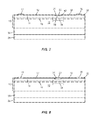
- FIG. 1 illustrates a cross-sectional portion of the active region of a III-nitride device according to the prior art.
- FIG. 2 illustrates a cross-sectional portion of the active region of another III-nitride device according to the prior art.
- FIG. 3 illustrates schematically the electric field lines near the gate of a device according to FIG. 1 .
- FIG. 4 illustrates schematically the electric field lines near the gate of the device according to FIG. 2 .
- FIG. 5 illustrates a cross-sectional portion of the active region of a III-nitride device according to the first embodiment of the present invention.
- FIG. 6 illustrates a cross-sectional portion of the active region of a III-nitride device according to the second embodiment of the present invention.
- FIG. 7 illustrates a cross-sectional portion of the active region of a III-nitride device according to the third embodiment of the present invention.
- FIG. 8 illustrates a cross-sectional portion of the active region of a III-nitride device according to the fourth embodiment of the present invention.
- FIGS. 9A-9C illustrates various embodiments of the present invention.
- 2-DEG 16 includes a reduced charge region 34 which resides under gate arrangement 22 .
- Reduced charge region 34 is preferably twice as wide as gate arrangement 22 , may extend beyond at least one edge of gate arrangement 22 , and is less conductive than adjacent regions of 2-DEG 16 when the 2-DEG is in the conductive state. That is, in the on state (when there is conduction between the power electrodes 18 , 29 ), region 34 include fewer carriers than regions of 2-DEG 16 adjacent each side thereof.
- the electric fields near the edges of gate arrangement 22 during the off state of the device are weaker compared to the prior art, which may allow for the omission of the field plate.
- reduced charge region 34 does not need to be positioned symmetrically relative to first (source) and second (drain) power electrodes 18 , 20 or with respect to gate arrangement 22 .
- reduced charge region 34 may be discontinuous and arranged in two portions 34 ′ 34 ′′ each at one side of gate arrangement 22 ( FIG. 9A ), may extend farther in the direction of the drain electrode ( FIG. 9B ), or may only extend in direction of the drain electrode ( FIG. 9C ) and include no portion extending beyond gate arrangement 22 toward the source electrode.
- the width of region 34 can be optimized and is expected to be between few tens to a few thousands of nanometers.
- gate arrangement 22 includes a schottky body 36 , which is schottky coupled to second III-nitride body 14 .
- Schottky body 36 may be any suitable schottky metal, for example, a nickel/gold stack, wherein the gold is atop the nickel.
- gate arrangement 22 includes gate insulation body 38 on second III-nitride body 14 , and gate electrode 40 , which is capacitively coupled to 2-DEG 16 (and particularly to reduced charge region 34 ) through insulation 38 .
- Gate insulation body 38 may be composed of silicon nitride, silicon dioxide, or any suitable gate insulation, while gate electrode 40 may be composed of any metallic or non-metallic conductive material. Examples of suitable materials for gate electrode 40 are nickel, titanium tungsten, titanium nitride, and polysilicon.
- negative charge may be introduced into second III-nitride body 14 to repel negative carriers (electrons) in the region 34 below gate arrangement 22 .
- the negative charge may be introduced by implantation of negatively charged ions or by plasma surface treatment.
- recess 42 may be formed in second III-nitride body 14 in which gate arrangement 22 is received.
- recess 42 can be configured to partially relieve the stress in second III-nitride body 14 so that a reduced charge region 34 according to the present invention can be obtained.
- recess 42 can be as wide as gate arrangement 22 , but may be wider (as schematically illustrated) without deviating from the scope and the spirit of the present invention.
- a field plate may be added to further enhance the breakdown capability of a device according to the present invention without deviating from the scope and spirit of the invention.
- first and second power electrodes 18 , 20 may be composed of Ti, Al, Ni, Au, or any other suitable metallic or non-metallic conductive material
- first III-nitride body 12 may be composed of GaN
- second III-nitride body 14 may be composed of MN
- transition layer 30 may be composed of a III-nitride material such as AlGaN
- substrate 28 may be composed of silicon.
- suitable substrate materials are silicon Carbide, or sapphire, or a material native to the III-nitride system, such as a GaN substrate.
Landscapes
- Engineering & Computer Science (AREA)
- Microelectronics & Electronic Packaging (AREA)
- Power Engineering (AREA)
- Physics & Mathematics (AREA)
- Ceramic Engineering (AREA)
- Condensed Matter Physics & Semiconductors (AREA)
- General Physics & Mathematics (AREA)
- Computer Hardware Design (AREA)
- Junction Field-Effect Transistors (AREA)
- Formation Of Insulating Films (AREA)
- Thin Film Transistor (AREA)
- Insulated Gate Type Field-Effect Transistor (AREA)
Abstract
Description
Claims (23)
Priority Applications (1)
| Application Number | Priority Date | Filing Date | Title |
|---|---|---|---|
| US15/191,863 US10340333B2 (en) | 2006-03-20 | 2016-06-24 | III-nitride power semiconductor device |
Applications Claiming Priority (5)
| Application Number | Priority Date | Filing Date | Title |
|---|---|---|---|
| US78405406P | 2006-03-20 | 2006-03-20 | |
| US11/725,430 US7408208B2 (en) | 2006-03-20 | 2007-03-19 | III-nitride power semiconductor device |
| PCT/US2007/006903 WO2007109265A2 (en) | 2006-03-20 | 2007-03-20 | Iii-nitrite power semiconductor device |
| US16274908A | 2008-10-17 | 2008-10-17 | |
| US15/191,863 US10340333B2 (en) | 2006-03-20 | 2016-06-24 | III-nitride power semiconductor device |
Related Parent Applications (2)
| Application Number | Title | Priority Date | Filing Date |
|---|---|---|---|
| PCT/US2007/006903 Continuation WO2007109265A2 (en) | 2006-03-20 | 2007-03-20 | Iii-nitrite power semiconductor device |
| US12/162,749 Continuation US9391185B2 (en) | 2006-03-20 | 2007-03-20 | III-nitride power semiconductor device |
Publications (2)
| Publication Number | Publication Date |
|---|---|
| US20160380046A1 US20160380046A1 (en) | 2016-12-29 |
| US10340333B2 true US10340333B2 (en) | 2019-07-02 |
Family
ID=38523050
Family Applications (4)
| Application Number | Title | Priority Date | Filing Date |
|---|---|---|---|
| US11/725,430 Active US7408208B2 (en) | 2006-03-20 | 2007-03-19 | III-nitride power semiconductor device |
| US12/162,749 Active 2028-03-06 US9391185B2 (en) | 2006-03-20 | 2007-03-20 | III-nitride power semiconductor device |
| US15/191,222 Active US9923052B2 (en) | 2006-03-20 | 2016-06-23 | III-nitride power semiconductor device |
| US15/191,863 Active 2028-01-20 US10340333B2 (en) | 2006-03-20 | 2016-06-24 | III-nitride power semiconductor device |
Family Applications Before (3)
| Application Number | Title | Priority Date | Filing Date |
|---|---|---|---|
| US11/725,430 Active US7408208B2 (en) | 2006-03-20 | 2007-03-19 | III-nitride power semiconductor device |
| US12/162,749 Active 2028-03-06 US9391185B2 (en) | 2006-03-20 | 2007-03-20 | III-nitride power semiconductor device |
| US15/191,222 Active US9923052B2 (en) | 2006-03-20 | 2016-06-23 | III-nitride power semiconductor device |
Country Status (5)
| Country | Link |
|---|---|
| US (4) | US7408208B2 (en) |
| JP (1) | JP5298006B2 (en) |
| CN (1) | CN101410975B (en) |
| DE (1) | DE112007000668B4 (en) |
| WO (1) | WO2007109265A2 (en) |
Families Citing this family (5)
| Publication number | Priority date | Publication date | Assignee | Title |
|---|---|---|---|---|
| US8455920B2 (en) * | 2007-05-23 | 2013-06-04 | International Rectifier Corporation | III-nitride heterojunction device |
| JP5655424B2 (en) * | 2010-08-09 | 2015-01-21 | サンケン電気株式会社 | Compound semiconductor device |
| JP5701805B2 (en) | 2012-03-28 | 2015-04-15 | 株式会社東芝 | Manufacturing method of nitride semiconductor Schottky diode |
| JP5715588B2 (en) * | 2012-03-28 | 2015-05-07 | 株式会社東芝 | Semiconductor device and manufacturing method thereof |
| JP6111821B2 (en) | 2013-04-25 | 2017-04-12 | 三菱電機株式会社 | Field effect transistor |
Citations (4)
| Publication number | Priority date | Publication date | Assignee | Title |
|---|---|---|---|---|
| US20020017648A1 (en) * | 2000-06-29 | 2002-02-14 | Kensuke Kasahara | Semiconductor device |
| US20050189561A1 (en) * | 2004-02-12 | 2005-09-01 | Kinzer Daniel M. | III-Nitride bidirectional switch |
| US7501669B2 (en) * | 2003-09-09 | 2009-03-10 | Cree, Inc. | Wide bandgap transistor devices with field plates |
| US7612390B2 (en) * | 2004-02-05 | 2009-11-03 | Cree, Inc. | Heterojunction transistors including energy barriers |
Family Cites Families (10)
| Publication number | Priority date | Publication date | Assignee | Title |
|---|---|---|---|---|
| US6593193B2 (en) * | 2001-02-27 | 2003-07-15 | Matsushita Electric Industrial Co., Ltd. | Semiconductor device and method for fabricating the same |
| WO2003032397A2 (en) * | 2001-07-24 | 2003-04-17 | Cree, Inc. | INSULTING GATE AlGaN/GaN HEMT |
| WO2004034475A1 (en) * | 2002-10-09 | 2004-04-22 | Matsushita Electric Industrial Co., Ltd. | Plasma oscillation switching device |
| JP2005203544A (en) * | 2004-01-15 | 2005-07-28 | Mitsubishi Electric Corp | Nitride semiconductor device and its manufacturing method |
| US8174048B2 (en) * | 2004-01-23 | 2012-05-08 | International Rectifier Corporation | III-nitride current control device and method of manufacture |
| US7382001B2 (en) * | 2004-01-23 | 2008-06-03 | International Rectifier Corporation | Enhancement mode III-nitride FET |
| JP4642366B2 (en) * | 2004-03-26 | 2011-03-02 | 日本碍子株式会社 | Semiconductor stacked structure, transistor element, and method of manufacturing transistor element |
| JP2006032552A (en) | 2004-07-14 | 2006-02-02 | Toshiba Corp | Semiconductor device containing nitride |
| JP4607506B2 (en) * | 2004-07-16 | 2011-01-05 | 株式会社東芝 | Semiconductor device |
| US7238560B2 (en) | 2004-07-23 | 2007-07-03 | Cree, Inc. | Methods of fabricating nitride-based transistors with a cap layer and a recessed gate |
-
2007
- 2007-03-19 US US11/725,430 patent/US7408208B2/en active Active
- 2007-03-20 US US12/162,749 patent/US9391185B2/en active Active
- 2007-03-20 CN CN2007800115658A patent/CN101410975B/en not_active Expired - Fee Related
- 2007-03-20 JP JP2009501508A patent/JP5298006B2/en not_active Expired - Fee Related
- 2007-03-20 DE DE112007000668T patent/DE112007000668B4/en not_active Expired - Fee Related
- 2007-03-20 WO PCT/US2007/006903 patent/WO2007109265A2/en active Application Filing
-
2016
- 2016-06-23 US US15/191,222 patent/US9923052B2/en active Active
- 2016-06-24 US US15/191,863 patent/US10340333B2/en active Active
Patent Citations (4)
| Publication number | Priority date | Publication date | Assignee | Title |
|---|---|---|---|---|
| US20020017648A1 (en) * | 2000-06-29 | 2002-02-14 | Kensuke Kasahara | Semiconductor device |
| US7501669B2 (en) * | 2003-09-09 | 2009-03-10 | Cree, Inc. | Wide bandgap transistor devices with field plates |
| US7612390B2 (en) * | 2004-02-05 | 2009-11-03 | Cree, Inc. | Heterojunction transistors including energy barriers |
| US20050189561A1 (en) * | 2004-02-12 | 2005-09-01 | Kinzer Daniel M. | III-Nitride bidirectional switch |
Also Published As
| Publication number | Publication date |
|---|---|
| JP2009530857A (en) | 2009-08-27 |
| CN101410975A (en) | 2009-04-15 |
| US20090039392A1 (en) | 2009-02-12 |
| US9391185B2 (en) | 2016-07-12 |
| JP5298006B2 (en) | 2013-09-25 |
| CN101410975B (en) | 2012-02-01 |
| US20160380046A1 (en) | 2016-12-29 |
| WO2007109265B1 (en) | 2008-05-15 |
| US7408208B2 (en) | 2008-08-05 |
| US20160380092A1 (en) | 2016-12-29 |
| DE112007000668T5 (en) | 2009-01-29 |
| WO2007109265A3 (en) | 2008-04-03 |
| DE112007000668B4 (en) | 2012-08-23 |
| US9923052B2 (en) | 2018-03-20 |
| WO2007109265A2 (en) | 2007-09-27 |
| US20080067548A1 (en) | 2008-03-20 |
Similar Documents
| Publication | Publication Date | Title |
|---|---|---|
| US11152499B2 (en) | Nitride semiconductor device and method for manufacturing same | |
| US9941399B2 (en) | Enhancement mode III-N HEMTs | |
| US10340333B2 (en) | III-nitride power semiconductor device | |
| JP5366798B2 (en) | Wide bandgap transistor with high efficiency and / or high power density | |
| US9640649B2 (en) | III-nitride power semiconductor with a field relaxation feature | |
| US9570438B1 (en) | Avalanche-rugged quasi-vertical HEMT | |
| US20080308813A1 (en) | High breakdown enhancement mode gallium nitride based high electron mobility transistors with integrated slant field plate | |
| JP4473201B2 (en) | Electronic devices | |
| JP2007180143A (en) | Nitride semiconductor element | |
| US20190081167A1 (en) | Nitride semiconductor device | |
| US20170104064A1 (en) | Nitride semiconductor device with asymmetric electrode tips | |
| JP2009253126A (en) | Semiconductor device | |
| US8969917B2 (en) | Semiconductor device and method for manufacturing same | |
| US8174051B2 (en) | III-nitride power device | |
| WO2007081807A2 (en) | Iii-nitride power semiconductor with a field relaxation feature | |
| JP6639260B2 (en) | Semiconductor device | |
| JP2010278137A (en) | Semiconductor device | |
| US20240105824A1 (en) | Barrier Structure for Sub-100 Nanometer Gate Length Devices |
Legal Events
| Date | Code | Title | Description |
|---|---|---|---|
| AS | Assignment |
Owner name: INFINEON TECHNOLOGIES AMERICAS CORP., CALIFORNIA Free format text: CHANGE OF NAME;ASSIGNOR:INTERNATIONAL RECTIFIER CORPORATION;REEL/FRAME:039003/0753 Effective date: 20150929 Owner name: INTERNATIONAL RECTIFIER CORPORATION, CALIFORNIA Free format text: ASSIGNMENT OF ASSIGNORS INTEREST;ASSIGNOR:HERMAN, THOMAS;REEL/FRAME:039003/0702 Effective date: 20080911 |
|
| STPP | Information on status: patent application and granting procedure in general |
Free format text: NOTICE OF ALLOWANCE MAILED -- APPLICATION RECEIVED IN OFFICE OF PUBLICATIONS |
|
| STPP | Information on status: patent application and granting procedure in general |
Free format text: PUBLICATIONS -- ISSUE FEE PAYMENT VERIFIED |
|
| STCF | Information on status: patent grant |
Free format text: PATENTED CASE |
|
| CC | Certificate of correction | ||
| MAFP | Maintenance fee payment |
Free format text: PAYMENT OF MAINTENANCE FEE, 4TH YEAR, LARGE ENTITY (ORIGINAL EVENT CODE: M1551); ENTITY STATUS OF PATENT OWNER: LARGE ENTITY Year of fee payment: 4 |