US10339359B2 - Display panel and display device - Google Patents
Display panel and display device Download PDFInfo
- Publication number
- US10339359B2 US10339359B2 US15/691,239 US201715691239A US10339359B2 US 10339359 B2 US10339359 B2 US 10339359B2 US 201715691239 A US201715691239 A US 201715691239A US 10339359 B2 US10339359 B2 US 10339359B2
- Authority
- US
- United States
- Prior art keywords
- light
- fingerprint recognition
- polarizer
- organic light
- fingerprint
- Prior art date
- Legal status (The legal status is an assumption and is not a legal conclusion. Google has not performed a legal analysis and makes no representation as to the accuracy of the status listed.)
- Active, expires
Links
- 239000000758 substrate Substances 0.000 claims abstract description 236
- 230000010287 polarization Effects 0.000 claims description 67
- 230000003287 optical effect Effects 0.000 claims description 48
- 239000000463 material Substances 0.000 claims description 38
- 239000011521 glass Substances 0.000 claims description 37
- 238000005538 encapsulation Methods 0.000 claims description 21
- 238000003860 storage Methods 0.000 claims description 15
- 239000003990 capacitor Substances 0.000 claims description 14
- 238000001514 detection method Methods 0.000 claims description 10
- 239000010409 thin film Substances 0.000 claims description 9
- 239000000853 adhesive Substances 0.000 claims description 6
- 230000001070 adhesive effect Effects 0.000 claims description 6
- 239000007788 liquid Substances 0.000 claims description 6
- 239000010410 layer Substances 0.000 description 277
- 239000010408 film Substances 0.000 description 149
- 239000011159 matrix material Substances 0.000 description 50
- 238000000034 method Methods 0.000 description 31
- 239000006059 cover glass Substances 0.000 description 23
- 239000013307 optical fiber Substances 0.000 description 18
- 230000031700 light absorption Effects 0.000 description 17
- 239000002346 layers by function Substances 0.000 description 16
- 229910052751 metal Inorganic materials 0.000 description 15
- 239000002184 metal Substances 0.000 description 15
- 230000008569 process Effects 0.000 description 14
- 238000002834 transmittance Methods 0.000 description 14
- 238000004519 manufacturing process Methods 0.000 description 13
- 238000010586 diagram Methods 0.000 description 11
- 230000035945 sensitivity Effects 0.000 description 11
- 230000000593 degrading effect Effects 0.000 description 9
- 238000005516 engineering process Methods 0.000 description 8
- 230000006698 induction Effects 0.000 description 8
- 239000007787 solid Substances 0.000 description 6
- 230000000903 blocking effect Effects 0.000 description 4
- 239000004642 Polyimide Substances 0.000 description 3
- 238000006073 displacement reaction Methods 0.000 description 3
- 238000009826 distribution Methods 0.000 description 3
- 238000002347 injection Methods 0.000 description 3
- 239000007924 injection Substances 0.000 description 3
- 229920001721 polyimide Polymers 0.000 description 3
- 229910021532 Calcite Inorganic materials 0.000 description 2
- 239000012790 adhesive layer Substances 0.000 description 2
- 230000008859 change Effects 0.000 description 2
- 239000011651 chromium Substances 0.000 description 2
- 239000003086 colorant Substances 0.000 description 2
- 230000007547 defect Effects 0.000 description 2
- 238000011161 development Methods 0.000 description 2
- 230000005684 electric field Effects 0.000 description 2
- 238000010292 electrical insulation Methods 0.000 description 2
- 230000005281 excited state Effects 0.000 description 2
- -1 gate Chemical class 0.000 description 2
- 239000011810 insulating material Substances 0.000 description 2
- 239000007769 metal material Substances 0.000 description 2
- 150000002739 metals Chemical class 0.000 description 2
- 238000003825 pressing Methods 0.000 description 2
- 239000002096 quantum dot Substances 0.000 description 2
- 239000010453 quartz Substances 0.000 description 2
- VYPSYNLAJGMNEJ-UHFFFAOYSA-N silicon dioxide Inorganic materials O=[Si]=O VYPSYNLAJGMNEJ-UHFFFAOYSA-N 0.000 description 2
- 125000006850 spacer group Chemical group 0.000 description 2
- 239000000126 substance Substances 0.000 description 2
- JBRZTFJDHDCESZ-UHFFFAOYSA-N AsGa Chemical compound [As]#[Ga] JBRZTFJDHDCESZ-UHFFFAOYSA-N 0.000 description 1
- VYZAMTAEIAYCRO-UHFFFAOYSA-N Chromium Chemical compound [Cr] VYZAMTAEIAYCRO-UHFFFAOYSA-N 0.000 description 1
- 239000004262 Ethyl gallate Substances 0.000 description 1
- 229910001218 Gallium arsenide Inorganic materials 0.000 description 1
- UCKMPCXJQFINFW-UHFFFAOYSA-N Sulphide Chemical compound [S-2] UCKMPCXJQFINFW-UHFFFAOYSA-N 0.000 description 1
- NIXOWILDQLNWCW-UHFFFAOYSA-N acrylic acid group Chemical group C(C=C)(=O)O NIXOWILDQLNWCW-UHFFFAOYSA-N 0.000 description 1
- 229910021417 amorphous silicon Inorganic materials 0.000 description 1
- 238000004458 analytical method Methods 0.000 description 1
- 230000005540 biological transmission Effects 0.000 description 1
- 229910052804 chromium Inorganic materials 0.000 description 1
- 238000004140 cleaning Methods 0.000 description 1
- 238000013461 design Methods 0.000 description 1
- 230000005283 ground state Effects 0.000 description 1
- 230000005525 hole transport Effects 0.000 description 1
- AMGQUBHHOARCQH-UHFFFAOYSA-N indium;oxotin Chemical compound [In].[Sn]=O AMGQUBHHOARCQH-UHFFFAOYSA-N 0.000 description 1
- 230000010354 integration Effects 0.000 description 1
- 239000004973 liquid crystal related substance Substances 0.000 description 1
- 230000007246 mechanism Effects 0.000 description 1
- 229910052755 nonmetal Inorganic materials 0.000 description 1
- 239000011368 organic material Substances 0.000 description 1
- 239000000049 pigment Substances 0.000 description 1
- 238000005498 polishing Methods 0.000 description 1
- 230000005855 radiation Effects 0.000 description 1
- 230000008707 rearrangement Effects 0.000 description 1
- 238000011160 research Methods 0.000 description 1
- 239000002210 silicon-based material Substances 0.000 description 1
- 238000006467 substitution reaction Methods 0.000 description 1
- 230000007704 transition Effects 0.000 description 1
- 238000012795 verification Methods 0.000 description 1
Images


Classifications
-
- G06K9/0004—
-
- G—PHYSICS
- G02—OPTICS
- G02B—OPTICAL ELEMENTS, SYSTEMS OR APPARATUS
- G02B5/00—Optical elements other than lenses
- G02B5/30—Polarising elements
- G02B5/3025—Polarisers, i.e. arrangements capable of producing a definite output polarisation state from an unpolarised input state
- G02B5/3033—Polarisers, i.e. arrangements capable of producing a definite output polarisation state from an unpolarised input state in the form of a thin sheet or foil, e.g. Polaroid
-
- G—PHYSICS
- G02—OPTICS
- G02B—OPTICAL ELEMENTS, SYSTEMS OR APPARATUS
- G02B5/00—Optical elements other than lenses
- G02B5/30—Polarising elements
- G02B5/3025—Polarisers, i.e. arrangements capable of producing a definite output polarisation state from an unpolarised input state
-
- G—PHYSICS
- G02—OPTICS
- G02F—OPTICAL DEVICES OR ARRANGEMENTS FOR THE CONTROL OF LIGHT BY MODIFICATION OF THE OPTICAL PROPERTIES OF THE MEDIA OF THE ELEMENTS INVOLVED THEREIN; NON-LINEAR OPTICS; FREQUENCY-CHANGING OF LIGHT; OPTICAL LOGIC ELEMENTS; OPTICAL ANALOGUE/DIGITAL CONVERTERS
- G02F1/00—Devices or arrangements for the control of the intensity, colour, phase, polarisation or direction of light arriving from an independent light source, e.g. switching, gating or modulating; Non-linear optics
- G02F1/01—Devices or arrangements for the control of the intensity, colour, phase, polarisation or direction of light arriving from an independent light source, e.g. switching, gating or modulating; Non-linear optics for the control of the intensity, phase, polarisation or colour
- G02F1/13—Devices or arrangements for the control of the intensity, colour, phase, polarisation or direction of light arriving from an independent light source, e.g. switching, gating or modulating; Non-linear optics for the control of the intensity, phase, polarisation or colour based on liquid crystals, e.g. single liquid crystal display cells
- G02F1/133—Constructional arrangements; Operation of liquid crystal cells; Circuit arrangements
- G02F1/1333—Constructional arrangements; Manufacturing methods
-
- G—PHYSICS
- G06—COMPUTING; CALCULATING OR COUNTING
- G06F—ELECTRIC DIGITAL DATA PROCESSING
- G06F3/00—Input arrangements for transferring data to be processed into a form capable of being handled by the computer; Output arrangements for transferring data from processing unit to output unit, e.g. interface arrangements
- G06F3/01—Input arrangements or combined input and output arrangements for interaction between user and computer
- G06F3/03—Arrangements for converting the position or the displacement of a member into a coded form
- G06F3/041—Digitisers, e.g. for touch screens or touch pads, characterised by the transducing means
- G06F3/0412—Digitisers structurally integrated in a display
-
- G06K9/2027—
-
- G06K9/2036—
-
- G—PHYSICS
- G06—COMPUTING; CALCULATING OR COUNTING
- G06V—IMAGE OR VIDEO RECOGNITION OR UNDERSTANDING
- G06V40/00—Recognition of biometric, human-related or animal-related patterns in image or video data
- G06V40/10—Human or animal bodies, e.g. vehicle occupants or pedestrians; Body parts, e.g. hands
- G06V40/12—Fingerprints or palmprints
- G06V40/13—Sensors therefor
- G06V40/1318—Sensors therefor using electro-optical elements or layers, e.g. electroluminescent sensing
-
- G—PHYSICS
- G09—EDUCATION; CRYPTOGRAPHY; DISPLAY; ADVERTISING; SEALS
- G09G—ARRANGEMENTS OR CIRCUITS FOR CONTROL OF INDICATING DEVICES USING STATIC MEANS TO PRESENT VARIABLE INFORMATION
- G09G3/00—Control arrangements or circuits, of interest only in connection with visual indicators other than cathode-ray tubes
- G09G3/20—Control arrangements or circuits, of interest only in connection with visual indicators other than cathode-ray tubes for presentation of an assembly of a number of characters, e.g. a page, by composing the assembly by combination of individual elements arranged in a matrix no fixed position being assigned to or needed to be assigned to the individual characters or partial characters
- G09G3/22—Control arrangements or circuits, of interest only in connection with visual indicators other than cathode-ray tubes for presentation of an assembly of a number of characters, e.g. a page, by composing the assembly by combination of individual elements arranged in a matrix no fixed position being assigned to or needed to be assigned to the individual characters or partial characters using controlled light sources
- G09G3/30—Control arrangements or circuits, of interest only in connection with visual indicators other than cathode-ray tubes for presentation of an assembly of a number of characters, e.g. a page, by composing the assembly by combination of individual elements arranged in a matrix no fixed position being assigned to or needed to be assigned to the individual characters or partial characters using controlled light sources using electroluminescent panels
- G09G3/32—Control arrangements or circuits, of interest only in connection with visual indicators other than cathode-ray tubes for presentation of an assembly of a number of characters, e.g. a page, by composing the assembly by combination of individual elements arranged in a matrix no fixed position being assigned to or needed to be assigned to the individual characters or partial characters using controlled light sources using electroluminescent panels semiconductive, e.g. using light-emitting diodes [LED]
- G09G3/3208—Control arrangements or circuits, of interest only in connection with visual indicators other than cathode-ray tubes for presentation of an assembly of a number of characters, e.g. a page, by composing the assembly by combination of individual elements arranged in a matrix no fixed position being assigned to or needed to be assigned to the individual characters or partial characters using controlled light sources using electroluminescent panels semiconductive, e.g. using light-emitting diodes [LED] organic, e.g. using organic light-emitting diodes [OLED]
- G09G3/3225—Control arrangements or circuits, of interest only in connection with visual indicators other than cathode-ray tubes for presentation of an assembly of a number of characters, e.g. a page, by composing the assembly by combination of individual elements arranged in a matrix no fixed position being assigned to or needed to be assigned to the individual characters or partial characters using controlled light sources using electroluminescent panels semiconductive, e.g. using light-emitting diodes [LED] organic, e.g. using organic light-emitting diodes [OLED] using an active matrix
- G09G3/3233—Control arrangements or circuits, of interest only in connection with visual indicators other than cathode-ray tubes for presentation of an assembly of a number of characters, e.g. a page, by composing the assembly by combination of individual elements arranged in a matrix no fixed position being assigned to or needed to be assigned to the individual characters or partial characters using controlled light sources using electroluminescent panels semiconductive, e.g. using light-emitting diodes [LED] organic, e.g. using organic light-emitting diodes [OLED] using an active matrix with pixel circuitry controlling the current through the light-emitting element
-
- G—PHYSICS
- G09—EDUCATION; CRYPTOGRAPHY; DISPLAY; ADVERTISING; SEALS
- G09G—ARRANGEMENTS OR CIRCUITS FOR CONTROL OF INDICATING DEVICES USING STATIC MEANS TO PRESENT VARIABLE INFORMATION
- G09G3/00—Control arrangements or circuits, of interest only in connection with visual indicators other than cathode-ray tubes
- G09G3/20—Control arrangements or circuits, of interest only in connection with visual indicators other than cathode-ray tubes for presentation of an assembly of a number of characters, e.g. a page, by composing the assembly by combination of individual elements arranged in a matrix no fixed position being assigned to or needed to be assigned to the individual characters or partial characters
- G09G3/34—Control arrangements or circuits, of interest only in connection with visual indicators other than cathode-ray tubes for presentation of an assembly of a number of characters, e.g. a page, by composing the assembly by combination of individual elements arranged in a matrix no fixed position being assigned to or needed to be assigned to the individual characters or partial characters by control of light from an independent source
- G09G3/3406—Control of illumination source
-
- H01L27/3234—
-
- H01L27/3244—
-
- H01L27/3246—
-
- H01L51/0097—
-
- H01L51/5253—
-
- H01L51/5268—
-
- H01L51/5281—
-
- H—ELECTRICITY
- H10—SEMICONDUCTOR DEVICES; ELECTRIC SOLID-STATE DEVICES NOT OTHERWISE PROVIDED FOR
- H10K—ORGANIC ELECTRIC SOLID-STATE DEVICES
- H10K50/00—Organic light-emitting devices
- H10K50/80—Constructional details
- H10K50/84—Passivation; Containers; Encapsulations
- H10K50/844—Encapsulations
-
- H—ELECTRICITY
- H10—SEMICONDUCTOR DEVICES; ELECTRIC SOLID-STATE DEVICES NOT OTHERWISE PROVIDED FOR
- H10K—ORGANIC ELECTRIC SOLID-STATE DEVICES
- H10K50/00—Organic light-emitting devices
- H10K50/80—Constructional details
- H10K50/85—Arrangements for extracting light from the devices
- H10K50/854—Arrangements for extracting light from the devices comprising scattering means
-
- H—ELECTRICITY
- H10—SEMICONDUCTOR DEVICES; ELECTRIC SOLID-STATE DEVICES NOT OTHERWISE PROVIDED FOR
- H10K—ORGANIC ELECTRIC SOLID-STATE DEVICES
- H10K50/00—Organic light-emitting devices
- H10K50/80—Constructional details
- H10K50/86—Arrangements for improving contrast, e.g. preventing reflection of ambient light
-
- H—ELECTRICITY
- H10—SEMICONDUCTOR DEVICES; ELECTRIC SOLID-STATE DEVICES NOT OTHERWISE PROVIDED FOR
- H10K—ORGANIC ELECTRIC SOLID-STATE DEVICES
- H10K59/00—Integrated devices, or assemblies of multiple devices, comprising at least one organic light-emitting element covered by group H10K50/00
- H10K59/10—OLED displays
- H10K59/12—Active-matrix OLED [AMOLED] displays
- H10K59/122—Pixel-defining structures or layers, e.g. banks
-
- H—ELECTRICITY
- H10—SEMICONDUCTOR DEVICES; ELECTRIC SOLID-STATE DEVICES NOT OTHERWISE PROVIDED FOR
- H10K—ORGANIC ELECTRIC SOLID-STATE DEVICES
- H10K59/00—Integrated devices, or assemblies of multiple devices, comprising at least one organic light-emitting element covered by group H10K50/00
- H10K59/60—OLEDs integrated with inorganic light-sensitive elements, e.g. with inorganic solar cells or inorganic photodiodes
- H10K59/65—OLEDs integrated with inorganic image sensors
-
- H—ELECTRICITY
- H10—SEMICONDUCTOR DEVICES; ELECTRIC SOLID-STATE DEVICES NOT OTHERWISE PROVIDED FOR
- H10K—ORGANIC ELECTRIC SOLID-STATE DEVICES
- H10K59/00—Integrated devices, or assemblies of multiple devices, comprising at least one organic light-emitting element covered by group H10K50/00
- H10K59/80—Constructional details
- H10K59/87—Passivation; Containers; Encapsulations
- H10K59/873—Encapsulations
-
- H—ELECTRICITY
- H10—SEMICONDUCTOR DEVICES; ELECTRIC SOLID-STATE DEVICES NOT OTHERWISE PROVIDED FOR
- H10K—ORGANIC ELECTRIC SOLID-STATE DEVICES
- H10K59/00—Integrated devices, or assemblies of multiple devices, comprising at least one organic light-emitting element covered by group H10K50/00
- H10K59/80—Constructional details
- H10K59/8791—Arrangements for improving contrast, e.g. preventing reflection of ambient light
-
- H—ELECTRICITY
- H10—SEMICONDUCTOR DEVICES; ELECTRIC SOLID-STATE DEVICES NOT OTHERWISE PROVIDED FOR
- H10K—ORGANIC ELECTRIC SOLID-STATE DEVICES
- H10K77/00—Constructional details of devices covered by this subclass and not covered by groups H10K10/80, H10K30/80, H10K50/80 or H10K59/80
- H10K77/10—Substrates, e.g. flexible substrates
- H10K77/111—Flexible substrates
-
- G—PHYSICS
- G02—OPTICS
- G02B—OPTICAL ELEMENTS, SYSTEMS OR APPARATUS
- G02B27/00—Optical systems or apparatus not provided for by any of the groups G02B1/00 - G02B26/00, G02B30/00
- G02B27/28—Optical systems or apparatus not provided for by any of the groups G02B1/00 - G02B26/00, G02B30/00 for polarising
- G02B27/281—Optical systems or apparatus not provided for by any of the groups G02B1/00 - G02B26/00, G02B30/00 for polarising used for attenuating light intensity, e.g. comprising rotatable polarising elements
-
- G—PHYSICS
- G09—EDUCATION; CRYPTOGRAPHY; DISPLAY; ADVERTISING; SEALS
- G09G—ARRANGEMENTS OR CIRCUITS FOR CONTROL OF INDICATING DEVICES USING STATIC MEANS TO PRESENT VARIABLE INFORMATION
- G09G2300/00—Aspects of the constitution of display devices
- G09G2300/08—Active matrix structure, i.e. with use of active elements, inclusive of non-linear two terminal elements, in the pixels together with light emitting or modulating elements
- G09G2300/0809—Several active elements per pixel in active matrix panels
- G09G2300/0842—Several active elements per pixel in active matrix panels forming a memory circuit, e.g. a dynamic memory with one capacitor
- G09G2300/0861—Several active elements per pixel in active matrix panels forming a memory circuit, e.g. a dynamic memory with one capacitor with additional control of the display period without amending the charge stored in a pixel memory, e.g. by means of additional select electrodes
-
- G—PHYSICS
- G09—EDUCATION; CRYPTOGRAPHY; DISPLAY; ADVERTISING; SEALS
- G09G—ARRANGEMENTS OR CIRCUITS FOR CONTROL OF INDICATING DEVICES USING STATIC MEANS TO PRESENT VARIABLE INFORMATION
- G09G2310/00—Command of the display device
- G09G2310/02—Addressing, scanning or driving the display screen or processing steps related thereto
- G09G2310/0243—Details of the generation of driving signals
- G09G2310/0251—Precharge or discharge of pixel before applying new pixel voltage
-
- G—PHYSICS
- G09—EDUCATION; CRYPTOGRAPHY; DISPLAY; ADVERTISING; SEALS
- G09G—ARRANGEMENTS OR CIRCUITS FOR CONTROL OF INDICATING DEVICES USING STATIC MEANS TO PRESENT VARIABLE INFORMATION
- G09G2310/00—Command of the display device
- G09G2310/02—Addressing, scanning or driving the display screen or processing steps related thereto
- G09G2310/0262—The addressing of the pixel, in a display other than an active matrix LCD, involving the control of two or more scan electrodes or two or more data electrodes, e.g. pixel voltage dependent on signals of two data electrodes
-
- G—PHYSICS
- G09—EDUCATION; CRYPTOGRAPHY; DISPLAY; ADVERTISING; SEALS
- G09G—ARRANGEMENTS OR CIRCUITS FOR CONTROL OF INDICATING DEVICES USING STATIC MEANS TO PRESENT VARIABLE INFORMATION
- G09G2354/00—Aspects of interface with display user
-
- H01L2251/5315—
-
- H01L2251/5338—
-
- H—ELECTRICITY
- H10—SEMICONDUCTOR DEVICES; ELECTRIC SOLID-STATE DEVICES NOT OTHERWISE PROVIDED FOR
- H10K—ORGANIC ELECTRIC SOLID-STATE DEVICES
- H10K2102/00—Constructional details relating to the organic devices covered by this subclass
- H10K2102/301—Details of OLEDs
- H10K2102/302—Details of OLEDs of OLED structures
- H10K2102/3023—Direction of light emission
- H10K2102/3026—Top emission
-
- H—ELECTRICITY
- H10—SEMICONDUCTOR DEVICES; ELECTRIC SOLID-STATE DEVICES NOT OTHERWISE PROVIDED FOR
- H10K—ORGANIC ELECTRIC SOLID-STATE DEVICES
- H10K2102/00—Constructional details relating to the organic devices covered by this subclass
- H10K2102/301—Details of OLEDs
- H10K2102/311—Flexible OLED
-
- Y—GENERAL TAGGING OF NEW TECHNOLOGICAL DEVELOPMENTS; GENERAL TAGGING OF CROSS-SECTIONAL TECHNOLOGIES SPANNING OVER SEVERAL SECTIONS OF THE IPC; TECHNICAL SUBJECTS COVERED BY FORMER USPC CROSS-REFERENCE ART COLLECTIONS [XRACs] AND DIGESTS
- Y02—TECHNOLOGIES OR APPLICATIONS FOR MITIGATION OR ADAPTATION AGAINST CLIMATE CHANGE
- Y02E—REDUCTION OF GREENHOUSE GAS [GHG] EMISSIONS, RELATED TO ENERGY GENERATION, TRANSMISSION OR DISTRIBUTION
- Y02E10/00—Energy generation through renewable energy sources
- Y02E10/50—Photovoltaic [PV] energy
- Y02E10/549—Organic PV cells
-
- Y—GENERAL TAGGING OF NEW TECHNOLOGICAL DEVELOPMENTS; GENERAL TAGGING OF CROSS-SECTIONAL TECHNOLOGIES SPANNING OVER SEVERAL SECTIONS OF THE IPC; TECHNICAL SUBJECTS COVERED BY FORMER USPC CROSS-REFERENCE ART COLLECTIONS [XRACs] AND DIGESTS
- Y02—TECHNOLOGIES OR APPLICATIONS FOR MITIGATION OR ADAPTATION AGAINST CLIMATE CHANGE
- Y02P—CLIMATE CHANGE MITIGATION TECHNOLOGIES IN THE PRODUCTION OR PROCESSING OF GOODS
- Y02P70/00—Climate change mitigation technologies in the production process for final industrial or consumer products
- Y02P70/50—Manufacturing or production processes characterised by the final manufactured product
Definitions
- the present disclosure generally relates to the display technology and, more particularly, relates to a display panel and a display device thereof.
- a fingerprint is a mark made by the pattern of ridges on the pad of a human finger, which is innate and unique for everyone.
- display devices with a fingerprint recognition function are emerging on the market, such as mobile phones, tablets and smart wearable devices, etc.
- a user can verify the permission only by touching the fingerprint recognition sensor of the display device, thereby simplifying the permission verification.
- the fingerprint recognition sensor is often provided in a non-display region of the display panel or on a surface opposite to the light exiting side of the display device.
- the user has to specifically touch the fingerprint recognition sensor to verify the permission, degrading the user experience.
- the fingerprint recognition sensor is disposed in the non-display region of the display panel, the screen-to-body ratio of the display panel is reduced, which is not in line with the development trend of narrow borders in the display panel.
- the gate, source and drain electrodes of the thin-film-transistor (TFT) in the pixel circuit which is arranged in the display region of the display panel are often made of metal, when the fingerprint recognition sensor is directly disposed in the display region of the display panel, light emitted from the light source of the fingerprint recognition sensor may be directly reflected by the gate, source and drain electrodes of the TFT, and then incident onto the fingerprint recognition sensor, generating noises and degrading the accuracy of the fingerprint recognition sensor. In addition, the light that is leaked from the organic light-emitting layer of the display panel may also be incident onto the fingerprint recognition sensor, generating noises and degrading the accuracy of the fingerprint recognition sensor.
- TFT thin-film-transistor
- the disclosed display panel and display device thereof are directed to solve one or more problems set forth above and other problems.
- the display panel comprises a display module comprising a first substrate and a first polarizer disposed on the first substrate, wherein the first substrate has an inner side facing the first polarizer and an opposite outer side, the first polarizer has an inner side facing the first substrate and an opposite outer side, and a light-exiting surface of the display module is arranged on the outer side of the first polarizer; a fingerprint recognition module disposed on the outer side of the first substrate and comprising a fingerprint recognition layer and a second polarizer, wherein the fingerprint recognition layer has an inner side facing the display module and an opposite outer side, and the second polarizer is disposed on the inner side of the fingerprint recognition layer; and a light source disposed on the inner side of the first polarizer.
- the fingerprint recognition layer is configured to recognize fingerprint based on fingerprint signal light, the fingerprint signal light being light emitted from the light source and then reflected to the fingerprint recognition layer by a touch object, the first polarizer is engaged with the second polarizer, such that the fingerprint signal light is transmitted through the first polarizer and the second polarizer without a light intensity loss, and the second polarizer is configured to reduce the light intensity of fingerprint noise light, the fingerprint noise light being light other than the fingerprint signal light.
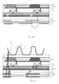
- FIG. 1 illustrates a schematic cross-sectional view of an exemplary display panel consistent with disclosed embodiments
- FIG. 2 a illustrates an exemplary optical path before light emitted from an organic light-emitting layer is reflected by a touch object consistent with disclosed embodiments
- FIG. 2 b illustrates an exemplary optical path after light emitted from an organic light-emitting layer is reflected by a touch object consistent with disclosed embodiments
- FIG. 3 illustrates an exemplary optical path of fingerprint noise light emitted from an organic light-emitting layer consistent with disclosed embodiments
- FIG. 4 illustrates a schematic cross-sectional view of another exemplary display panel consistent with disclosed embodiments
- FIG. 5 illustrates a schematic cross-sectional view of another exemplary display panel consistent with disclosed embodiments
- FIG. 6 a illustrates another exemplary optical path before light emitted from a backlight source is reflected by a touch object consistent with disclosed embodiments
- FIG. 6 b illustrates another exemplary optical path after light emitted from a backlight source is reflected by a touch object consistent with disclosed embodiments
- FIG. 7 a illustrates an exemplary optical path before fingerprint noise light emitted from a backlight source is reflected by a touch object consistent with disclosed embodiments
- FIG. 7 b illustrates an exemplary optical path after fingerprint noise light emitted from a backlight source is reflected by a touch object consistent with disclosed embodiments
- FIG. 8 illustrates a schematic cross-sectional view of another exemplary display panel consistent with disclosed embodiments
- FIG. 9 a illustrates a circuit diagram of an exemplary fingerprint sensor in an exemplary fingerprint recognition module consistent with disclosed embodiments
- FIG. 9 b illustrates a schematic cross-sectional view of an exemplary fingerprint sensor in an exemplary fingerprint recognition module consistent with disclosed embodiments
- FIG. 10 a illustrates a schematic top view of another exemplary display panel consistent with disclosed embodiments
- FIG. 10 b illustrates a partial enlarged schematic view of an exemplary S 1 region in FIG. 10 a consistent with disclosed embodiments
- FIG. 10 c illustrates a schematic A 1 -A 2 sectional view of another exemplary display panel in FIG. 10 a consistent with disclosed embodiments;
- FIG. 10 d illustrates an exemplary first closed loop and an exemplary second closed loop consistent with disclosed embodiments
- FIG. 10 e illustrates a partial enlarged schematic view of another exemplary S 1 region in FIG. 10 a consistent with disclosed embodiments
- FIG. 11 illustrates a schematic top view of another exemplary display panel consistent with disclosed embodiments
- FIG. 12 a illustrates a schematic cross-sectional view of another exemplary display panel consistent with disclosed embodiments
- FIG. 12 b illustrates a partial enlarged schematic view of an exemplary S 1 region in FIG. 12 a consistent with disclosed embodiments
- FIG. 12 c illustrates a circuit diagram of an exemplary pixel driving circuit consistent with disclosed embodiments
- FIG. 12 d illustrates an exemplary driving diagram of an exemplary pixel driving circuit consistent with disclosed embodiments
- FIG. 13 illustrates a schematic cross-sectional view of another exemplary display panel consistent with disclosed embodiments
- FIG. 14 a illustrates a schematic three-dimensional (3D) view of an exemplary display panel consistent with disclosed embodiments
- FIG. 14 b illustrates a schematic B 1 -B 2 sectional view of an exemplary display panel in FIG. 14 a consistent with disclosed embodiments;
- FIG. 15 illustrates a schematic cross-sectional view of another exemplary display panel consistent with disclosed embodiments
- FIG. 16 illustrates a schematic cross-sectional view of another exemplary display panel consistent with disclosed embodiments
- FIG. 17 illustrates a schematic cross-sectional view of another exemplary display panel consistent with disclosed embodiments
- FIG. 18 illustrates a schematic cross-sectional view of another exemplary display panel consistent with disclosed embodiments
- FIG. 19 illustrates a schematic cross-sectional view of another exemplary display panel consistent with disclosed embodiments.
- FIG. 20 illustrates a schematic cross-sectional view of another exemplary display panel consistent with disclosed embodiments
- FIG. 21 a illustrates a schematic top view of another exemplary display panel consistent with disclosed embodiments
- FIG. 21 b illustrates a schematic C 1 -C 2 sectional view of another exemplary display panel in FIG. 21 a consistent with disclosed embodiments;
- FIG. 22 illustrates a fingerprint recognition principle of an exemplary fingerprint recognition module consistent with disclosed embodiments
- FIG. 23 a illustrates a schematic top view of another exemplary display panel consistent with disclosed embodiments
- FIG. 23 b illustrates a schematic D 1 -D 2 sectional view of another exemplary display panel in FIG. 23 a consistent with disclosed embodiments;
- FIG. 24 a illustrates a schematic top view of an exemplary angle-limiting film consistent with disclosed embodiments
- FIG. 24 b illustrates a schematic E 1 -E 2 sectional view of an exemplary angle-limiting film in FIG. 24 a consistent with disclosed embodiments;
- FIG. 24 c illustrates a schematic cross-sectional view of another exemplary display panel consistent with disclosed embodiments
- FIG. 24 d illustrates a diffusing distance of an exemplary angle-limiting film in FIG. 24 a consistent with disclosed embodiments
- FIG. 24 e illustrates a schematic top view of another exemplary angle-limiting film consistent with disclosed embodiments
- FIG. 25 a illustrates a schematic top view of another exemplary angle-limiting film consistent with disclosed embodiments
- FIG. 25 b illustrates a schematic F 1 -F 2 sectional view of another exemplary angle-limiting film in FIG. 25 a consistent with disclosed embodiments;
- FIG. 25 c illustrates a schematic top view of another exemplary angle-limiting film consistent with disclosed embodiments
- FIG. 26 a illustrates a schematic top view of another exemplary angle-limiting film consistent with disclosed embodiments
- FIG. 26 b illustrates a schematic cross-sectional view along an extending direction of optical fibers in an exemplary angle-limiting film in FIG. 26 a consistent with disclosed embodiments;
- FIG. 26 c illustrates a diffusing distance of another exemplary angle-limiting film in FIG. 26 a consistent with disclosed embodiments
- FIG. 27 a illustrates a schematic top view of another exemplary angle-limiting film consistent with disclosed embodiments
- FIG. 27 b illustrates a schematic G 1 -G 2 sectional view of another exemplary angle-limiting film in FIG. 27 a consistent with disclosed embodiments;
- FIG. 28 a illustrates a schematic cross-sectional view of another exemplary display panel consistent with disclosed embodiments
- FIG. 28 b illustrates a partial top view of another exemplary display panel in FIG. 28 a consistent with disclosed embodiments
- FIG. 28 c illustrates a scanning diagram at a fingerprint recognition stage of another exemplary display panel in FIG. 28 a consistent with disclosed embodiments
- FIG. 28 d illustrates a detailed schematic view of another exemplary display panel in FIG. 28 a consistent with disclosed embodiments
- FIG. 29 illustrates a crosstalk in an existing display panel
- FIG. 30 illustrates a schematic cross-sectional view of another exemplary display panel consistent with disclosed embodiments
- FIG. 31 a illustrates a schematic cross-sectional view of another exemplary display panel consistent with disclosed embodiments
- FIG. 31 b illustrates a schematic H 1 -H 2 sectional view of another exemplary display panel in FIG. 31 a consistent with disclosed embodiments;
- FIG. 32 a illustrates a schematic cross-sectional view of another exemplary display panel consistent with disclosed embodiments
- FIG. 32 b illustrates a schematic 11 - 12 sectional view of another exemplary display panel in FIG. 32 a consistent with disclosed embodiments;
- FIG. 33 a illustrates a schematic cross-sectional view of another exemplary display panel consistent with disclosed embodiments
- FIG. 33 b illustrates a schematic cross-sectional view of another exemplary display panel consistent with disclosed embodiments
- FIG. 33 c illustrates a schematic top view of exemplary display panels in FIG. 33 a and FIG. 33 b consistent with disclosed embodiments;
- FIG. 34 a illustrates a scanning diagram at a fingerprint recognition stage of another exemplary display panel consistent with disclosed embodiments
- FIG. 34 b illustrates a scanning diagram at a fingerprint recognition stage of another exemplary display panel consistent with disclosed embodiments
- FIG. 35 a illustrates a schematic top view of an exemplary first light-emitting unit array consistent with disclosed embodiments
- FIG. 35 b illustrates a schematic top view of another exemplary first light-emitting unit array consistent with disclosed embodiments
- FIG. 35 c illustrates a schematic top view of another exemplary first light-emitting unit array consistent with disclosed embodiments
- FIG. 36 a illustrates an exemplary square array scanning method of an exemplary display panel consistent with disclosed embodiments
- FIG. 36 b illustrates an exemplary hexagonal array scanning method of an exemplary display panel consistent with disclosed embodiments
- FIG. 37 illustrates a flowchart of an exemplary display panel fingerprint recognition method consistent with disclosed embodiments.
- FIG. 38 illustrates an exemplary display device consistent with disclosed embodiments.
- a fingerprint is a mark made by the pattern of ridges on the pad of a human finger, which is innate and unique for everyone.
- fingerprint recognition technology we can put a person with his fingerprints, by comparing his fingerprints and pre-stored fingerprint data to verify his true identity, which is called as fingerprint recognition technology.
- the analysis of fingerprints for matching purposes generally requires the comparison of several features of the print pattern. These include patterns, which are aggregate characteristics of ridges, and minutia points, which are unique features found within the patterns.
- optical fingerprint recognition technology is emerging in our daily life, which has been the most deeply-researched, the most widely used, and the most mature technology in biological detection technology.
- the principle of optical fingerprint recognition technology is explained as follows.
- the light source in the display panel emits light to a user finger, and the light reflected by the user finger is incident onto a fingerprint sensor, and corresponding light signals are collected by the fingerprint sensor. Due to the specific lines on the fingerprint, the light reflected at different positions of the user finger has different light intensity, and then the fingerprint sensor collects different light signals, according to which the user's true identity is determined.
- the present disclosure provides an improved display panel and display device, which is able to reduce the noise signal in the fingerprint recognition module, and improve the accuracy of the fingerprint recognition.
- the display panel comprises:
- the light-exiting surface of the display module is disposed on the outer side of the first polarizer
- the fingerprint recognition module is disposed on the outer side of the first substrate
- the fingerprint recognition module comprises the fingerprint recognition layer and the second polarizer disposed on the inner side of the fingerprint recognition layer.
- the light emitted from the inner side of the first polarizer is reflected by the touch object (such as a user finger) to form the fingerprint signa light, during which the first polarizer is engaged with the second polarizer, such that the fingerprint signal light is transmitted through the first polarizer and the second polarizer without a light intensity loss.
- the second polarizer at least reduces the light intensity of the fingerprint noise light.
- the crosstalk caused by the fingerprint noise may be suppressed, the signal-to-noise ratio may be improved, and the accuracy of the fingerprint recognition module may be improved.
- the light source may be an existing light source in the display panel, such that the thickness of the display panel may not be increased, the fabrication process may be simplified, and the fabrication cost may be reduced.
- the fingerprint recognition module has an inner side facing the display module and an opposite outer side, and an external source may be disposed on the outer side of the fingerprint recognition module and configured as the light source.
- the position of the light source for example, the distance between the light source and the fingerprint recognition layer
- the light source with the desired lighting properties may be selected (for example, a highly collimated light source may be selected to reduce the interference between the fingerprint signal light).
- the light source is not limited by the present disclosure, as long as the light source is disposed on the inner side of the first polarizer and the fingerprint recognition module can detect the fingerprint signal light.
- the fingerprint noise light may include part of the light leaked out from the light source of the display module to the fingerprint recognition module, and/or the light emitted from the external light source and then reflected by the metals (e.g., gate, source, drain electrodes of a thin-film-transistors) in the display module.
- the metals e.g., gate, source, drain electrodes of a thin-film-transistors
- the second polarizer may be configured to be a linear polarizer or a circular polarizer, which is able to reduce the light intensity of the fingerprint noise light by half.
- the second polarizer may be configured to be a circular polarizer, which is able to completely eliminate the fingerprint noise light.
- the first polarizer when second polarizer is a linear polarizer, the first polarizer may be configured to have the same polarization direction as the second polarizer, such that the fingerprint signal light is transmitted through the first polarizer and the second polarizer without a light intensity loss.
- the first polarizer when second polarizer is a circular polarizer, the first polarizer may be configured to be a circular polarizer which is engaged with the second polarizer, such that the fingerprint signal light is transmitted through the first polarizer and the second polarizer without a light intensity loss.
- FIG. 1 illustrates a schematic cross-sectional view of an exemplary display panel consistent with disclosed embodiments.
- the display panel may comprise a display module 1 and a fingerprint recognition module 2 .
- the display module 1 may comprise a first substrate 10 and a first polarizer 11 disposed on the first substrate 10 .
- the first polarizer 11 may have an inner side facing the first substrate 10 and an opposite outer side.
- the light-exiting surface of the display module 1 may be disposed on the outer side of the first polarizer 11 .
- the first substrate 10 may have an inner side facing the first polarizer 11 and an opposite outer side.
- the fingerprint recognition module 2 may be disposed on the outer side of the first substrate 10 .
- the fingerprint recognition module 2 may comprise a fingerprint recognition layer 21 and a second polarizer 22 .
- the fingerprint recognition layer 21 may have an inner side facing the display module 1 and an opposite outer side, and the second polarizer 22 may disposed on the inner side of the fingerprint recognition layer 21 .
- the fingerprint recognition layer 21 may be configured to identify the fingerprint based on fingerprint signal light, which is emitted from a light source and then reflected to the fingerprint recognition layer 21 by a touch object.
- the display module 1 may further comprise an organic light-emitting layer 12 disposed between the first substrate 10 and the first polarizer 11 for generating light for displaying an image.
- the display module 1 may also comprise any other appropriate components, which is not limited by the present disclosure.
- the organic light-emitting layer 12 may comprise a plurality of organic light-emitting units.
- the organic light-emitting layer 12 may comprise a red organic light-emitting unit 121 , a green organic light-emitting unit 122 , and a blue organic light-emitting unit 123 .
- the fingerprint recognition layer 21 may comprise a plurality of fingerprint recognition units 211 .
- the organic light-emitting layer 12 may be multiplexed as the light source for fingerprint recognition.
- a plurality of organic light-emitting units and a plurality of fingerprint recognition units may be arranged in an array, respectively.
- the plurality of organic light-emitting units may be arranged in correspondence with the plurality of fingerprint recognition units.
- the organic light-emitting unit is multiplexed as the light source, the light emitted from one organic light-emitting unit may be received by one or more fingerprint recognition units corresponding to the organic light-emitting unit.
- the display panel may include a display region, where the organic light-emitting unit and the fingerprint recognition unit are disposed.
- the fingerprint recognition may be realized in the display region of the display panel.
- the light emitted from the organic light-emitting layer 12 may be incident onto the touch object, which is often a user finger.
- the fingerprint is composed of a series of ridges 41 and valleys 42 disposed on the skin surface of the fingertip.
- the light, which is received by the fingerprint recognition unit 42 after being respectively reflected by the ridges 41 and the valley 42 may be different in light intensity.
- the current signals converted from the light intensity of the light respectively reflected by the ridges 41 and the valley 42 may be different in magnitude, based on which fingerprint may be recognized.
- the touch object may also be a palm
- the fingerprint recognition unit may realize the detection and recognition functions based on the palmprint.
- the organic light-emitting layer 12 When the organic light-emitting layer 12 functions as a light source for both image display and fingerprint recognition, the organic light-emitting layer 12 has to emit light at both the display stage and the fingerprint recognition stage.
- the display stage all the organic light-emitting units in the organic light-emitting layer may be provided with a driving signal for light emission, while at the fingerprint recognition stage, a part of the organic light-emitting units in the organic light-emitting layer may be provided with a driving signal for light emission.
- the display module 1 may further include a first display driving circuit 19 , which may output a driving signal for driving at least one of the organic light-emitting units to emit light at the fingerprint recognition stage, thereby providing a light source to the fingerprint recognition module 2 .
- the first display driving circuit 19 may output a driving signal for driving at least one of the red organic light-emitting unit and the green organic light-emitting unit to emit light.
- the display panel may include a touch function layer, where the structure and the position of the touch function layer are not limited by the present disclosure as long as the touch position on the screen can be detected.
- the first display driving circuit 19 may output a driving signal to drive the organic light-emitting units in the region corresponding to the finger touch position to emit light.
- the first polarizer 11 may comprise a first linear polarizer
- the second polarizer 22 may comprise a second linear polarizer.
- the first and second polarizers may have the same polarization direction, i.e., the optical axes of the first and second polarizers may be arranged in the same direction.
- the solid arrows indicate the light emitted from the organic light-emitting layer 12 toward the light exiting surface and the light reflected by the touch object to form the fingerprint signal light.
- the dashed arrow indicates the light that is leaked out from the organic light-emitting layer 12 to the fingerprint recognition module 2
- the light emitted from the organic light-emitting layer may be converted into linearly polarized light by the first polarizer 11 .
- the reflected light which is the fingerprint signal light may still be linearly polarized light, and the polarization direction is not changed.
- the fingerprint signal light may be transmitted through the first polarizer 11 without a light loss. Because the first and second polarizers have the same polarization direction, the fingerprint signal light may also be transmitted through the second polarizer 22 without a light loss, and then incident onto the fingerprint recognition unit 211
- the light leaked out from the red organic light-emitting unit 121 is substantially uniform in the respective polarization directions. After being transmitted through the second polarizer 22 , the transmitted light has only one polarization direction, and the light intensity thereof is approximately reduced by half. Thus, when upon being incident onto the fingerprint recognition unit 211 , the light leaked out from the organic light-emitting unit may have significantly reduced light intensity.
- the light intensity of the fingerprint noise light is relatively reduced while the light intensity of the fingerprint light is substantially the same.
- the signal-to-noise ratio of the fingerprint recognition module 2 may be improved, thereby improving the accuracy of the fingerprint recognition module 2 .
- the display panel may be a rigid display panel.
- the first substrate 10 may be a first glass substrate.
- the display module 1 may further include a second glass substrate 13 , and the organic light-emitting layer 12 may be disposed between the first glass substrate 10 and the second glass substrate 13 .
- the first glass substrate 10 and the second glass substrate 13 may be supported by spacers 15 , and an air gap may be formed between the first glass substrate 10 and the second glass substrate 13 .
- the thickness of the air gap may be approximately 4 ⁇ m.
- the display panel may also include a cover glass or cover lens 14 .
- the first polarizer 11 may have an inner side facing the organic light-emitting layer 12 and an opposite outer side.
- the cover glass 14 may be attached to the outer side of the first polarizer 11 by liquid optical clear adhesive (LOCA).
- LOCA liquid optical clear adhesive
- the thickness of the display module 1 may be approximately 1410 ⁇ m.
- the fingerprint recognition module 2 may further include a second substrate 20 having an inner side facing the display module 1 and an opposite outer side.
- the fingerprint recognition layer 21 may be disposed on the inner side of the second substrate 20 . That is, the fingerprint recognition layer 21 may be directly fabricated on the inner side of the second substrate 20 , simplifying the arrangement of the fingerprint recognition layer 21 . Meanwhile, the second substrate 20 may also protect the fingerprint recognition layer 21 .
- the second polarizer 22 may be attached to the first substrate 10 through a liquid optical clear adhesive (LOCA) (not drawn in FIG. 1 ), through which the display module 1 and the fingerprint recognition module 2 may be attached to each other to form the display panel.
- LOCA liquid optical clear adhesive
- the first polarizer 11 may include a first quarter-wave plate and a third linear polarizer stacked together.
- the third linear polarizer may have an inner side facing the organic light-emitting layer 12 and an opposite outer side, and the first quarter-wave plate may be disposed on the inner side of the third linear polarizer.
- the second polarizer 22 may include a second quarter-wave plate and a fourth linear polarizer stacked together.
- the fourth linear polarizer may have an inner side facing the organic light-emitting layer 12 and an opposite outer side, and the second quarter-wave plate may be disposed on the inner side of the fourth linear polarizer.
- the first quarter-wave plate and the second quarter-wave plate may have the same material and the same thickness.
- the angle from the optical axis of the first quarter-wave plate to the polarization direction of the third linear polarizer may be configured to be approximately 45°.
- the angle from the optical axis of the second quarter-wave plate to the polarization direction of the fourth linear polarizer may be configured to be approximately ⁇ 45°.
- the angle from the optical axis of the first quarter-wave plate to the polarization direction of the third linear polarizer may be configured to be approximately ⁇ 45°.
- the angle from the optical axis of the second quarter-wave plate to the polarization direction of the fourth linear polarizer may be configured to be approximately 45°.
- the formed first polarizer and second polarizer may both be circular polarizers.
- FIG. 2 a illustrates an exemplary optical path before light emitted from an organic light-emitting layer is reflected by a touch object consistent with disclosed embodiments.
- FIG. 2 b illustrates an exemplary optical path after light emitted from an organic light-emitting layer is reflected by a touch object consistent with disclosed embodiments;
- FIG. 2 a and FIG. 2 b counterclockwise is defined as the positive direction when facing the propagation direction of the light. As shown in FIG. 1 , the light before and after being reflected by the touch object have different propagation directions.
- the first quarter-wave plate and the second quarter-wave plate may both be calcite, and the e-axis of the first quarter-wave plate and the e-axis of the second quarter-wave plate are defined as the optical axis, respectively.
- the angle from the e-axis of the first quarter-wave 111 plate to the polarization direction P of the third linear polarizer 112 may be configured to be approximately ⁇ 45°.
- the natural light NL_ 1 emitted from the organic light-emitting layer 12 may pass through the first quarter-wave plate 111 and become natural light NL_ 2 which is substantially remain the same as the natural light NL_ 1 .
- the NL_ 2 may pass through the third linear polarizer 112 to be converted into linearly polarized light NL_ 3 having the same polarization direction P as the third linear polarizer 112 . That is, the polarization direction of the converted linearly polarized light NL_ 3 may be in the second and fourth quadrants.
- the linearly polarized light NL_ 3 in FIG. 2 a may be reflected by the touch body to form the fingerprint signal light FSL_ 1 in FIG. 2 b , which is still linearly polarized light with substantially the same polarization direction (i.e., polarization direction P).
- the angle from the e-axis of the first quarter-wave plate 111 to the polarization direction P of the third linear polarizer 112 now becomes 45°, and the polarization direction of the fingerprint signal light is in the first and third quadrants, as shown in FIG. 2 b.
- the fingerprint signal light FSL_ 1 may be transmitted through the third linear polarizer 112 to become the fingerprint signal light FSL_ 2 having substantially the same polarization state and the light intensity.
- the fingerprint signal light FSL_ 2 may be transmitted through the first quarter-wave plate 111 to become left-handed circular polarized light FSL_ 3 having substantially the same light intensity.
- the left-handed circular polarized light FSL_ 3 may be transmitted through the second quarter-wave plate 221 to become linearly polarized light FSL_ 4 with a polarization direction in the second and fourth quadrants and substantially the same light intensity.
- the linearly polarized light FSL_ 4 may pass through the fourth linear polarizer 222 having the same polarization direction as the FSL_ 4 to become linearly polarized light FSL_ 5 with substantially the same light intensity.
- FIG. 3 illustrates an exemplary optical path of fingerprint noise light emitted from an organic light-emitting layer consistent with disclosed embodiments.
- the fingerprint noise light FNL_ 1 emitted from the organic light-emitting layer may be directly incident onto the second polarizer.
- the angle from the e-axis of the second quarter-wave plate 221 to the polarization direction of the fourth linear polarizer 222 may be configured to be approximately ⁇ 45°.
- the polarization direction of the fourth linear polarizer 222 is in the second and fourth quadrants.
- the fingerprint noise light FNL_ 1 may be transmitted through the second quarter-wave plate 221 to become fingerprint noise light FNL_ 2 which is still natural light.
- the fingerprint noise light FNL_ 2 may pass through the fourth linear polarizer 222 to become linear polarized light FNL_ 3 having a same polarization direction as the fourth linear polarizer 222 , and the light intensity of FNL_ 3 is reduced to half.
- the second polarizer 222 may reduce the light intensity of the fingerprint noise light, thereby improving the signal-to-noise ratio of fingerprint recognition.
- FIG. 4 illustrates a schematic cross-sectional view of another exemplary display panel consistent with disclosed embodiments. The similarities between FIG. 1 and FIG. 4 are not repeated here, while certain difference may be explained.
- the display panel may be a flexible display panel.
- the first substrate 10 may be a flexible substrate.
- the display module 1 may further comprises a thin film encapsulation layer 16 , which replaces the second glass substrate 13 in FIG. 1 .
- the thin film encapsulation layer 16 may cover the organic light-emitting layer 12 .
- FIG. 5 illustrates a schematic cross-sectional view of another exemplary display panel consistent with disclosed embodiments. The similarities between FIG. 1 and FIG. 5 are not repeated here, while certain difference may be explained.
- the display panel may comprise a display module 1 , a fingerprint recognition module 2 , and a backlight source 3 .
- the display module 1 may comprise a first substrate 10 , a first polarizer 11 disposed on the first substrate 10 , and an organic light-emitting layer 12 disposed between the first substrate 10 and the first polarizer 11 for displaying images.
- the first polarizer 11 may have an inner side facing the first substrate 10 and an opposite outer side.
- the light-exiting surface of the display module 1 may be disposed on the outer side of the first polarizer 11 .
- the first substrate 10 may have an inner side facing the first polarizer 11 and an opposite outer side.
- the fingerprint recognition module 2 may be disposed on the outer side of the first substrate 10 .
- the fingerprint recognition module 2 may comprise a fingerprint recognition layer 21 and a second polarizer 22 .
- the fingerprint recognition layer 21 may have an inner side facing the display module 1 and an opposite outer side, and the second polarizer 22 may disposed on the inner side of the fingerprint recognition layer 21 .
- the fingerprint recognition layer 21 may be configured to identify the fingerprint based on the fingerprint signal light, which is emitted from a light source and then reflected to the fingerprint recognition layer 21 by a touch object.
- the fingerprint recognition module 2 may have an inner side facing the display module 1 and an opposite outer side.
- the backlight source 3 may be disposed on the outer side of the fingerprint recognition module 2 .
- the backlight source 3 may be configured to be a light source for the fingerprint recognition module 2 .
- the organic light-emitting layer 12 may comprise a plurality of organic light-emitting units.
- the organic light-emitting layer 12 may comprise a red organic light-emitting unit 121 , a green organic light-emitting unit 122 , and a blue organic light-emitting unit 123 .
- the fingerprint recognition layer 21 may comprise a plurality of fingerprint recognition units 211 .
- the display panel may include a display region and a non-display region surrounding the display region, and the organic light-emitting unit and the fingerprint recognition unit may be disposed in the display region.
- the fingerprint recognition may be realized in the display region of the display panel.
- the organic light-emitting layer 12 may emit light for displaying images, while the backlight source 3 may be configured as a light source for the fingerprint recognition module 2 . That is, at the display stage, the backlight source 3 may not emit light while the organic light-emitting layer 12 may emit light, such that the image display may not be affected. At the fingerprint recognition stage, the organic light-emitting layer 12 may not emit light while the backlight source 3 may emit light, such that the interference on the fingerprint recognition, which is caused by the light leaked out from the organic light-emitting layer 12 as well as the light reflected by the touch object to the fingerprint recognition unit 121 , may be suppressed.
- the display module 1 in FIG. 5 may further comprise a second display driving circuit 18 , which may not output a display driving signal for driving the organic light-emitting layer to emit light at the fingerprint recognition stage, and not output a detection driving signal for driving the backlight source to emit light at the display stage.
- a second display driving circuit 18 may not output a display driving signal for driving the organic light-emitting layer to emit light at the fingerprint recognition stage, and not output a detection driving signal for driving the backlight source to emit light at the display stage.
- the first polarizer 11 may include a first quarter-wave plate and a third linear polarizer stacked together.
- the third linear polarizer may have an inner side facing the organic light-emitting layer 12 and an opposite outer side, and the first quarter-wave plate may be disposed on the inner side of the third linear polarizer.
- the second polarizer 22 may include a second quarter-wave plate and a fourth linear polarizer stacked together.
- the fourth linear polarizer may have an inner side facing the organic light-emitting layer 12 and an opposite outer side, and the second quarter-wave plate may be disposed on the inner side of the fourth linear polarizer.
- the first quarter-wave plate and the second quarter-wave plate may have the same material and the same thickness.
- the angle from the optical axis of the first quarter-wave plate to the polarization direction of the third linear polarizer may be configured to be approximately 45°.
- the angle from the optical axis of the second quarter-wave plate to the polarization direction of the fourth linear polarizer may be configured to be approximately ⁇ 45°.
- the angle from the optical axis of the first quarter-wave plate to the polarization direction of the third linear polarizer may be configured to be approximately ⁇ 45°.
- the angle from the optical axis of the second quarter-wave plate to the polarization direction of the fourth linear polarizer may be configured to be approximately 45°.
- the formed first polarizer and second polarizer may both be circular polarizers.
- FIG. 6 a illustrates another exemplary optical path before light emitted from a light source is reflected by a touch object consistent with disclosed embodiments.
- FIG. 6 b illustrates another exemplary optical path after light emitted from a light source is reflected by a touch object consistent with disclosed embodiments.
- FIG. 6 a and FIG. 6 b counterclockwise is defined as the positive direction when facing the propagation direction of the fingerprint signal light.
- the first quarter-wave plate and the second quarter-wave plate may both be calcite, and the e-axis of the first quarter-wave plate and the e-axis of the second quarter-wave plate is defined as the optical axis, respectively.
- the light before and after being reflected by the touch object have different propagation directions.
- the solid arrows indicate the light emitted from the backlight source 3 toward the light exiting surface, as well as, the light reflected by the touch object to form the fingerprint signal light.
- the dashed arrow indicates the light that is leaked out from the backlight source 3 to the fingerprint recognition module 2
- the angle from the e-axis of the first quarter-wave plate 111 to the polarization direction P of the third linear polarizer 112 may be configured to be approximately ⁇ 45°.
- the angle from the e-axis of the second quarter-wave plate 221 to the polarization direction P of the fourth linear polarizer 222 may be configured to be approximately 45°.
- the natural light NL_ 1 emitted from the backlight source 3 may pass through the fourth linear polarizer 222 , and become linearly polarized light NL_ 2 with a polarization direction in the first and third quadrants.
- the linearly polarized light NL_ 2 with the polarization direction in the first and third quadrants may pass through the second quarter-wave plate 221 , and become left-handed circular polarized light NL_ 3 .
- the left-handed circular polarized light NL_ 3 may pass through the first quarter-wave plate 111 , and become linearly polarized light NL_ 4 with a polarization direction in the second and fourth quadrants, which is the same as the polarization direction P of the third linear polarizer 112 .
- the linearly polarized light NL_ 4 with the polarization direction in the second and fourth quadrants may pass through the third linear polarizer 112 to become linearly polarized light NL_ 5 without a polarization direction change, i.e., the linearly polarized light NL_ 5 with the same polarization as the third linear polarizer 112 may be incident onto the touch object.
- the angle from the e-axis of the first quarter-wave plate 111 to the polarization direction P of the third linear polarizer 112 may be configured to be approximately 45°.
- the angle from the e-axis of the second quarter-wave plate 221 to the polarization direction P of the fourth linear polarizer 222 may be configured to be approximately ⁇ 45°.
- the linearly polarized light NL_ 5 in FIG. 6 a may be incident onto the touch object.
- the linearly polarized light NL_ 5 may be reflected by the touch object to become the linearly polarized fingerprint signal light FSL_ 1 in FIG. 6 b without a polarization direction change. Facing the prorogation direction of the fingerprint signal light FSL_ 1 , the polarization direction of the linearly polarized fingerprint signal light FSL_ 1 may be in the first and third quadrants.
- the linearly polarized fingerprint signal light FSL_ 1 may pass through the third linear polarizer 112 and become the linearly polarized fingerprint signal light FSL_ 2 with substantially the same polarization direction and light intensity.
- the linearly polarized fingerprint signal light FSL_ 2 may pass through the first quarter-wave plate 111 and become left-handed circular polarized fingerprint signal light FSL_ 3 with substantially the same light intensity.
- the left-handed circular polarized fingerprint signal light FSL_ 3 may pass through the second quarter-wave plate 221 and become linearly polarized fingerprint signal light FSL_ 4 with a polarization direction in the second and fourth quadrants and with substantially the same light intensity.
- the linearly polarized fingerprint signal light FSL_ 4 may pass through the fourth linear polarizer 222 having a same polarization direction as the linearly polarized fingerprint signal light FSL_ 4 and become the linearly polarized fingerprint signal light FSL_ 5 with substantially the same light intensity.
- FIG. 7 a illustrates an exemplary optical path before fingerprint noise light emitted from a backlight source is reflected by a touch object consistent with disclosed embodiments.
- FIG. 7 b illustrates an exemplary optical path after fingerprint noise light emitted from a backlight source is reflected by a touch object consistent with disclosed embodiments.
- counterclockwise is defined as the positive direction when facing the propagation direction of the light.
- the angle from the e-axis of the second quarter-wave plate 221 to the polarization direction P of the fourth linear polarizer 222 may be configured to be approximately 45°.
- the natural light NL_ 1 emitted from the backlight source 3 may pass through the fourth linear polarizer 222 and become linearly polarized light NL_ 2 with a polarization direction in the first and third quadrants.
- the linearly polarized light NL_ 2 with a polarization direction in the first and third quadrants may pass through the second quarter-wave plate 221 and become left-handed circular polarized light NL_ 3 .
- the left-handed circular polarized light NL_ 3 may be incident onto a metal layer (e.g., an electrode in the organic light-emitting layer 12 in FIG. 5 ), then reflected by the metal layer, becoming right-handed circular polarized fingerprint noise light FNL_ 1 in FIG. 7 b.
- a metal layer e.g., an electrode in the organic light-emitting layer 12 in FIG. 5
- the angle from the e-axis of the second quarter-wave plate 221 to the polarization direction P of the fourth linear polarizer 222 may be configured to be approximately ⁇ 45°.
- the right-handed circular polarized fingerprint noise light FNL_ 1 may pass through the second quarter-wave plate 221 and become linearly polarized light FNL_ 2 with a polarization direction in the first and third quadrants.
- the polarization direction of the linearly polarized light FNL_ 2 may be perpendicular to the polarization direction P of the fourth linear polarizer 222 .
- the linearly polarized light FNL_ 2 may not pass through the fourth linear polarizer 222 to be incident onto the fingerprint recognition units 211 . Accordingly, the fourth linear polarizer 222 may be able to eliminate the fingerprint noise light reflected by the metal layers in the display module 1 , and the signal-to-noise ratio of the fingerprint recognition may be improved.
- the display panel may be a rigid display panel.
- the first substrate 10 may be a first glass substrate.
- the display module 1 may further include a second glass substrate 13 , the organic light-emitting layer 12 may be disposed between the first glass substrate 10 and the second glass substrate 13 .
- the first glass substrate 10 and the second glass substrate 13 may be supported by spacers 15 , and an air gap may be formed between the first glass substrate 10 and the second glass substrate 13 .
- the thickness of the air gap may be approximately 4 ⁇ m.
- the display panel may also include a cover glass or cover lens 14 .
- the first polarizer 11 may have an inner side facing the organic light-emitting layer 12 and an opposite outer side.
- the cover glass 14 may be attached to the outer side of the first polarizer 11 by liquid optical clear adhesive (LOCA).
- LOCA liquid optical clear adhesive
- the thickness of the display module 1 may be approximately 1410 ⁇ m.
- the fingerprint recognition module 2 may further include a second substrate 20 having an inner side facing the display module 1 and an opposite outer side.
- the fingerprint recognition layer 21 may be disposed on the inner side of the second substrate 20 . That is, the fingerprint recognition layer 21 may be directly fabricated on the inner side of the second substrate 20 , facilitating the arrangement of the fingerprint recognition layer 21 . Meanwhile, the second substrate 20 may also protect the fingerprint recognition layer 21 .
- the second polarizer 22 may be attached to the first substrate 10 through an optical adhesive layer including liquid optical clear adhesive (LOCA) (not drawn in FIG. 5 ), through which the display module 1 and the fingerprint recognition module 2 may be attached to each other to form the display panel.
- LOCA liquid optical clear adhesive
- FIG. 8 illustrates a schematic cross-sectional view of another exemplary display panel consistent with disclosed embodiments. The similarities between FIG. 5 and FIG. 8 are not repeated here, while certain difference may be explained.
- the display panel may be a flexible display panel.
- the first substrate 10 may be a flexible substrate
- the display module 1 may further comprises a thin film encapsulation layer 16 , which replaces the second glass substrate 13 in
- the thin film encapsulation layer 16 may cover the organic light-emitting layer 12 .
- optical axis direction of the quarter-wave plate and the polarization direction of the linear polarizer shown in FIGS. 2 a , 6 a and 6 b are for illustrative purposes, and are not intended to limit the scope of the present disclosure.
- the optical axis direction of the first quarter-wave plate and the optical axis direction of the second quarter-wave plate have no specific relationship
- the polarization direction of the third linear polarizer and the polarization direction of the fourth linear polarizer have no specific relationship, as long as the angle from the optical axis of the first quarter-wave plate to the polarization direction of the third linear polarizer, and the angle from the fourth quarter-wave plate to the polarization direction of the fourth linear polarizer satisfy the limiting conditions of the disclosed embodiments.
- a fingerprint recognition unit may comprise a fingerprint sensor.
- FIG. 9 a illustrates a circuit diagram of an exemplary fingerprint sensor in an exemplary fingerprint recognition module consistent with disclosed embodiments.
- FIG. 9 b illustrates a schematic cross-sectional view of an exemplary fingerprint sensor in an exemplary fingerprint recognition module consistent with disclosed embodiments.
- the fingerprint sensor may include a photodiode D, a storage capacitor C, and a thin-film-transistor (TFT) T.
- the photodiode D may have a positive electrode D 1 electrically connected to the first electrode of the storage capacitor C, and a negative electrode D 2 electrically connected to the second electrode of the storage capacitor C and the source electrode Ts of the thin-film-transistor T.
- the gate electrode Tg of the thin-film-transistor T may be electrically connected to a switch control line Gate, and the drain Td of the thin-film-transistor T may be electrically connected to a signal detection line Data.
- the photodiode D may convert the fingerprint signal light into a current signal.
- the switch control line Gate may control the thin-film-transistor T to turn on, and the current signal may be transmitted to the signal detection line Data by the thin-film-transistor T, thereby realizing the fingerprint recognition according to the current signal.
- the present disclosure also provides certain exemplary display panels.
- the present disclosure provides an exemplary display panel where the organic light-emitting layer is multiplexed as a light source for fingerprint recognition.
- FIG. 10 a illustrates a schematic top view of another exemplary display panel consistent with disclosed embodiments.
- FIG. 10 b illustrates a partial enlarged schematic view of an exemplary S 1 region in FIG. 10 a consistent with disclosed embodiments.
- FIG. 10 c illustrates a schematic A 1 -A 2 sectional view of another exemplary display panel in FIG. 10 a consistent with disclosed embodiments;
- the display panel may comprise a first substrate 10 , a plurality of organic light-emitting units 120 , and at least one fingerprint recognition unit 211 .
- the plurality of organic light-emitting units 120 may be disposed on the first substrate 10 .
- the organic light-emitting unit 120 may have an inner side facing the viewers and an opposite outer side facing the first substrate 10 .
- the fingerprint recognition unit 211 may be disposed on the outer side of the organic light-emitting units 120 , i.e., the fingerprint recognition unit 211 may be disposed between the organic light-emitting units 120 and the first substrate 10 .
- the fingerprint recognition unit 211 may be configured to recognize or identify the fingerprint based on the light reflected by the touch object (such as finger) to the fingerprint recognition unit 211 .
- the plurality of organic light-emitting units 120 may comprise a plurality of red organic light-emitting units 121 , a plurality of green organic light-emitting units 122 , and a plurality of blue organic light-emitting units 123 .
- Each organic light-emitting unit may have the inner side facing the light-exiting surface of the display panel and the outer side far away from the light-exiting surface of the display panel.
- At the fingerprint recognition stage, at least one of the red organic light-emitting unit 121 and the green organic light-emitting unit 122 may be configured as the light source for the fingerprint recognition unit 211 to emit light. At least one of the red organic light-emitting unit 121 and the green organic light-emitting unit 122 , which is configured as the light source for the fingerprint recognition unit 211 , may have the area of a light-transparent region at the outer side of the organic light-emitting unit 120 smaller than the blue organic light-emitting unit 123 .
- the first substrate 1 may be an array substrate.
- each organic light-emitting unit 120 may have an inner side far away from the first substrate 10 and an opposite outer side facing the first substrate 10 .
- a first electrode 313 , a light-emitting function layer 311 , and a second electrode 314 may be sequentially disposed on the inner side of the organic light-emitting unit 120 .
- the organic light-emitting units 120 may include the red organic light-emitting units 121 , the green organic light-emitting units 122 , and the blue organic light-emitting units 123 .
- Each organic light-emitting unit 120 may include a light-emitting function layer 311 .
- the light-emitting function layer 311 may have an inner side facing the light-exiting surface of the display panel and an opposite outer side far away from the light-exiting surface of the display panel.
- the light-emitting function layer 311 in the organic light-emitting unit 120 may a light-transparent region 37 and an opaque region 36 at the outer side of the light-emitting function layer 311 .
- the light-exiting surface of the display panel may be arranged at the outer side of the organic light-emitting unit 120 .
- the light-emitting functional layer 311 may include a first auxiliary function layer, a light-emitting material or luminescent material layer, and a second auxiliary function layer.
- the first auxiliary functional layer may be a hole-type auxiliary functional layer, and may have a multilayer structure comprising, for example, one or more layers of a hole injection layer (HIL), a hole transport layer (HTL), and an electron blocking layer (EBL).
- the second auxiliary functional layer may be an electron-type auxiliary functional layer, and may have a multilayer structure comprising, for example, one or more layers of an electron transport layer (ETL), an electron injection layer (EIL), and a hole blocking layer (HBL).
- ETL electron transport layer
- EIL electron injection layer
- HBL hole blocking layer
- electrons from the second electrode 314 and holes the first electrode 313 may be injected into the luminescent material layer in the luminescent functional layer 311 , and then recombined to generate excitons.
- the excitons migrate under the applied electric field, and the energy is transferred to the light-emitting molecules in the luminescent material.
- the electrons are stimulated to transit from the ground state to the excited state.
- the electrons at the excited state may release the energy through the radiation transition, thereby generating light.
- the first electrode 313 may be an anode and the second electrode 314 may be a cathode. In another embodiment, the first electrode 313 may be a cathode, the second electrode 314 may be an anode, which is not limited by the present disclosure.
- the display panel may comprise a plurality of organic light-emitting units 120 and at least one fingerprint recognition unit 211 disposed on the first substrate 10 .
- the plurality of organic light-emitting units 120 may comprise a plurality of red organic light-emitting units 121 , a plurality of green organic light-emitting units 122 , and a plurality of blue organic light-emitting units 123 .
- the red organic light-emitting unit 121 , the green organic light-emitting units 122 , and the plurality of blue organic light-emitting units 123 may emit light according to a predetermined sequence.
- the light emitted by the blue organic light-emitting unit 123 has substantially short wavelength while the respective layers (e.g., organic insulating layers, inorganic insulating layers, polarizers, etc.) in the display panel strongly absorb light of short wavelength, the light emitted by the blue organic light-emitting unit 123 has lower light transmittance as compared to that of the red organic light-emitting unit 121 and green organic light-emitting unit 122 .
- the respective layers e.g., organic insulating layers, inorganic insulating layers, polarizers, etc.
- At least one of the red organic light-emitting unit 121 and the green organic light-emitting unit 122 may be configured to be the light source for the fingerprint recognition unit 211 and, meanwhile, the at least one of the red organic light-emitting unit 121 and the green organic light-emitting unit 122 , which is configured to be the light source for the fingerprint recognition unit 211 , may be configured to have the area of the light-transparent region at the outer side of the organic light-emitting unit 120 smaller than the blue organic light-emitting unit 123 .
- the organic light-emitting unit configured as the light source for the fingerprint recognition unit 211 has a smaller area of the light-transparent region, stray light which is directly incident onto the fingerprint recognition unit 211 without being reflected by the touch object (e.g., finger) may be reduced.
- the stray light which is directly incident onto the fingerprint recognition unit 211 without being reflected by the touch object (e.g., finger) may not carry the fingerprint information, as a comparison, the light reflected by the touch body may carry the fingerprint information.
- the noise in the fingerprint recognition may be suppressed, and the accuracy of the fingerprint recognition may be improved.
- the display panel may also include a second substrate 20 having an inner side facing the display module 1 and an opposite outer side.
- the first substrate 10 may have an inner side facing the organic light-emitting units 120 and an opposite outer side, and the second substrate 20 may be disposed on the outer side of the first substrate 10 .
- the fingerprint recognition units 211 may be disposed between the second substrate 20 and the first substrate 10 .
- the fingerprint recognition unit 211 and the second substrate 20 may be configured as a part of the fingerprint recognition module 2 , and the fingerprint recognition module 2 may also comprise a plurality of metal connection lines and IC drive circuits (not drawn in FIG. 10 c ).
- each organic light-emitting unit 120 may have the inner side facing the viewers and the outer side facing the first substrate 10 .
- the first electrode 313 , the light-emitting function layer 311 , and the second electrode 314 may be sequentially disposed on the inner side of the organic light-emitting unit 120 .
- the first electrode 313 may be a reflective electrode which may include, for example, an indium tin oxide (ITO) conductive layer, a reflective electrode layer (Ag), and an ITO conductive layer sequentially stacked.
- the ITO conductive layer comprises materials of a high work function, which may facilitate the hole injections.
- the light-emitting functional layer 311 of the red organic light-emitting unit 121 , the light-emitting functional layer 311 of the green organic light-emitting unit 122 , and the light-emitting functional layer 311 of the blue organic light-emitting unit 123 may be spaced apart from each other by a pixel-defining layer 312 .
- both the red organic light-emitting unit 121 and the green organic light-emitting unit 122 may be configured as the light source for the fingerprint recognition.
- the area of the first electrode 313 in the red organic light-emitting unit 121 and the area of the first electrode 313 in the green organic light-emitting unit 122 each may be larger than the area of the first electrode 313 in the blue organic light-emitting unit 123 .
- the light emitted from the light-emitting function layer 311 in the organic light-emitting unit 120 towards the first substrate 10 may be blocked by the first electrode 313 , which is disposed between the light-emitting function layer 311 and the fingerprint recognition unit 211 .
- the reflective electrodes (i.e., the first electrodes 313 ) in the red organic light-emitting unit 121 and green organic light-emitting unit 122 which are configured as the light source for the fingerprint recognition may be further extended outwards, for example, in the arrangement direction of the first electrodes 313 , thereby reducing the stray light incident onto the fingerprint recognition unit 211 and improving the accuracy of the fingerprint recognition.
- the area of the reflective electrode 313 in the blue organic light-emitting unit 123 may substantially remain the same, while the area of the reflective electrode 313 in the red organic light-emitting unit 121 and the area of the reflective electrode 313 in the green organic light-emitting unit 122 each may be expanded to block the stray light, as compared to the area of the reflective electrode in the existing display panel.
- the reflective electrode 313 may be arranged adjacent to or in contact with the light-emitting functional layer 311 , such that the light emitted from the light-emitting functional layer 311 towards the first substrate 10 may be substantially close to the edge of the reflective electrode 313 .
- the reflective electrode 313 may be configured to extend a predetermined distance to prevent the light emitted from the light-emitting function layer from being directly incident onto the fingerprint recognition unit 211 . Further, when the reflective electrode 313 is extended to a certain extent, the reflective electrode 313 may completely prevent the stray light from being incident onto the fingerprint recognition unit 211 , thereby greatly improving the accuracy of the fingerprint recognition.
- a ratio between the area of the first electrode 313 and the area of the light-emitting function layer 311 may be approximately in the range of 1.2 to 6.
- a ratio between the area of the first electrode 313 and the area of the light-emitting function layer 311 may be approximately in the range of 1 to 1.2.
- the opaque region 36 in FIG. 10 b may be the orthogonal projection of the first electrode 313 in the organic light-emitting unit 120 onto the first substrate 10 .
- the red organic light-emitting unit 121 and the green organic light-emitting unit 122 are configured as the light source of the fingerprint recognition unit 211
- the blue organic light-emitting unit 123 is not configured as the light source of the fingerprint recognition unit 211
- the ratio between the area of the opaque region 36 and the area of the light-emitting function layer 311 in the red organic light-emitting unit 121 and the ratio between the area of the opaque region 36 and the area of the light-emitting function layer 311 in the green organic light-emitting unit 122 each may be larger than the ratio between the area of the opaque region 36 and the area of the light-emitting function layer 311 in the blue organic light-emitting unit 123 .
- the first electrode 313 may effectively prevent the light emitted from the light-emitting function layer from being directly incident onto the fingerprint recognition unit 211 . That is, the stray light may be effectively suppressed, the noise in the fingerprint recognition may be reduced, and the accuracy of the fingerprint recognition may be improved.
- the organic light-emitting unit 120 which is configured as the light source for the fingerprint recognition unit 211
- the stray light may be more effectively blocked by the first electrode 313 , or more stray light may be blocked by the first electrode 313 .
- the ratio between the area of the first electrode 313 and the area of the light-emitting function layer 311 is approximately 6, the first electrode may be able to block most of the stray light, greatly improving the accuracy of the fingerprint recognition.
- FIG. 10 d illustrates an exemplary first closed loop and an exemplary second closed loop consistent with disclosed embodiments.
- the orthogonal projection of the border of the first electrode 313 in the organic light-emitting unit 120 may form a first closed loop 101
- the orthogonal projection of the border of the light-emitting function layer 311 in the organic light-emitting unit 120 may form a second closed loop 102 .
- the first closed loop 101 may surround the second closed loop 102 .
- the second closed loop 102 may have a corresponding point providing a short distance L between the point of the first closed loop 101 and the corresponding point of the second closed loop 102 . That is, the distance range between the first closed loop 101 and the second closed loop 102 may include a set of the shortest distances L corresponding to all the points on the first closed loop 101 .
- the distance range between the first closed loop 101 and the second closed loop 102 may represent the range of the extending length of the first electrode in either direction in the plane of the first electrode.
- the distance between the first closed loop 101 and the second closed loop 102 may be approximately in a range of 3 ⁇ m to 30 ⁇ m That is, the range of the extending length of the first electrode in either direction in the plane of the first electrode may be approximately in a range of 3 ⁇ m to 30 ⁇ m.
- the extending length of the first electrode in either direction in the plane of the first electrode may be approximately in a range of 3 ⁇ m to 30 ⁇ m.
- the first electrode may effectively reduce the stray light and improve the accuracy of fingerprint recognition.
- FIG. 10 e illustrates a partial enlarged schematic view of another exemplary S 1 region in FIG. 10 a consistent with disclosed embodiments.
- the red organic light-emitting unit 121 may be configured as the light source of the fingerprint recognition unit 211 .
- the red organic light-emitting unit 121 may have the area of the light-transparent region at the outer side of the red organic light-emitting unit 121 smaller than the blue organic light-emitting unit 123 .
- the red organic light-emitting unit 121 may have the area of the light-transparent region at the outer side of the red organic light-emitting unit 121 smaller than the green organic light-emitting unit 122 .
- the light-emitting layer in the red organic light-emitting unit 121 may have an inner side facing the light-exiting surface of the display panel and an opposite outer side far away from the light-exiting surface of the display panel. Because only the red organic light-emitting unit is used as the light source for fingerprint recognition, it may be only necessary to block the light emitted from the outer side of the light-emitting layer in the red organic light-emitting unit 121 , for example, only the first electrode in the red organic light-emitting unit 121 may have to be extended.
- the first electrodes in the blue organic light-emitting unit 123 and green organic light-emitting unit 122 may not have to extended and, meanwhile, both the green organic light-emitting unit 122 and the blue organic light-emitting unit 123 may have a light-transparent region of the organic light-emitting unit larger than the red organic light-emitting unit 121 .
- the accuracy of the fingerprint recognition may be ensured, while the light-transparent regions of the organic light-emitting units may be sufficiently large to transmit the light reflected by the touch object (e.g., finger), thereby increasing the light intensity of the fingerprint signal light detected by the fingerprint recognition unit.
- the touch object e.g., finger
- the light intensity of the fingerprint signal light detected by the fingerprint recognition unit may be increased by raising the operating voltage of the red organic light-emitting unit 121 .
- only the green organic light-emitting unit 122 may be configured as the light source of the fingerprint recognition unit 211 .
- the green organic light-emitting unit 122 may have the area of the light-transparent region at the outer side of the green organic light-emitting unit 122 smaller than the blue organic light-emitting unit 123 .
- the green organic light-emitting unit 122 may have the area of the light-transparent region at the outer side of the green organic light-emitting unit 122 smaller than the red organic light-emitting unit 121 .
- FIG. 11 illustrates a schematic top view of another exemplary display panel consistent with disclosed embodiments.
- the area of the light-emitting function layer in the blue organic light-emitting unit 123 may be larger than the area of the light-emitting functional layer in the red organic light-emitting unit 121 . Meanwhile, the area of the light-emitting function layer in the blue organic light-emitting unit 123 may be larger than the area of the light-emitting function layer in the green organic light-emitting unit 122 .
- the material of the light-emitting function layer of the blue organic light-emitting unit has a shorter life than the materials of the light-emitting functional layer in the red organic light-emitting mechanism and blue organic light-emitting unit, the area of the light-emitting function layer in the blue organic light-emitting unit may be desired to be larger, and the light-emitting function layer of the blue organic light-emitting unit may be able to be operated at a lower voltage.
- the operating voltage of the light-emitting functional layer in the red organic light-emitting unit 121 and the green organic light-emitting unit 122 may be set as approximately 3 V
- the operating voltage of the light-emitting functional layer in the blue organic light-emitting unit 123 may be set as approximately 2 V, thereby improving the lifetime of the blue organic light-emitting unit 123 . Accordingly, the lifetime of the red organic light-emitting unit, green organic light-emitting unit and blue organic light-emitting unit may be balanced, and the lifetime of the entire display panel may be improved.
- FIG. 12 a illustrates a schematic cross-sectional view of another exemplary display panel consistent with disclosed embodiments.
- FIG. 12 b illustrates a partial enlarged schematic view of an exemplary S 1 region in FIG. 12 a consistent with disclosed embodiments.
- the display panel may comprise a first substrate 10 and a plurality of pixel driving circuits 133 arranged on the first substrate 10 .
- Each pixel driving circuit 133 may be electrically connected to a corresponding organic light-emitting unit 120
- the fingerprint recognition unit 211 may be disposed between the first substrate 10 and the organic light-emitting unit 120 .
- FIG. 12 a shows three pixel driving circuits 133 , and each of the pixel driving circuits 133 may be electrically connected to the first electrode 313 in the corresponding organic light-emitting unit 120 .
- the fingerprint recognition units 211 , metal connecting lines, and an IC driving circuit may form a fingerprint recognition module, which may be embedded inside the display panel. Because the fingerprint recognition module is embedded inside the display panel, the thickness of the display panel may be reduced, and the thin-and-light design of the display panel may be realized.
- the pixel driving circuit 133 corresponding to the organic light-emitting unit 120 configured as the light source for the fingerprint recognition unit 211 when being projected onto the first substrate 10 , may have a larger orthogonal projection than, the pixel driving circuit 133 corresponding to the organic light-emitting unit 120 not configured as the light source for the fingerprint recognition unit 211 .
- the fingerprint recognition unit 211 may be arranged between the pixel driving circuit 133 and the first substrate 10 .
- the pixel driving circuits 133 may comprise a plurality of scanning lines 34 and a plurality of data lines 35 .
- the scanning lines 34 and data lines 35 in the pixel driving circuits 133 which are corresponding to the organic light-emitting unit 120 configured as the light source for the fingerprint recognition unit 211 , may be widened, thereby blocking the stray light.
- the position or the size of the opaque elements in the pixel driving circuits 133 which are corresponding to the organic light-emitting unit 120 configured as the light source for the fingerprint recognition unit 211 , may be modified, thereby blocking the stray light without affecting the original function of the opaque elements.
- the position of the capacitive metal plate 38 may be changed, such that in addition to the capacitance storage function, the capacitive metal plate 38 may also be able to block the stray light.
- FIG. 12 c illustrates a circuit diagram of an exemplary pixel driving circuit consistent with disclosed embodiments.
- FIG. 12 d illustrates an exemplary driving diagram of an exemplary pixel driving circuit consistent with disclosed embodiments.
- the scanning lines 34 in FIG. 12 b may be a signal control line, a first scanning line, and a second scanning line in the pixel drive circuit in FIG. 12 c .
- the data line 35 in FIG. 12 b may be a data line in the pixel drive circuit in FIG. 12 c .
- the capacitive metal plate 38 in FIG. 12 b may be a storage capacitor C 1 in the pixel driving circuit in FIG. 12 c . It is understood that the gate electrode, the source electrode and other non-transparent component of the first TFT T 1 and the second TFT T 2 in the pixel driving circuit may also be configured to block the stray light.
- the pixel driving circuit may include a data line, a first scanning line, a second scanning line, a signal control line, a light-emitting device, a storage capacitor C 1 , a driving transistor DTFT and five switching transistors T 1 to T 5 .
- the first TFT T 1 may have a gate electrode electrically connected to the signal control line, a source electrode electrically connected to a first level terminal, and a drain electrode electrically connected to a first electrode of the storage capacitor C 1 .
- the second switching transistor T 2 may have a gate electrode electrically connected to the first scanning line, a source electrode electrically connected to the ground, and a drain electrode electrically connected to a second electrode of the storage capacitor C 1 .
- the third switching transistor T 3 may have a gate electrode electrically connected to the first scanning line, and a source electrode electrically connected to the second electrode of the storage capacitor C 1 .
- the fourth switching transistor T 4 may have a gate electrode electrically connected to the first scanning line, a source electrode electrically connected to the data line, and a drain electrode electrically connected to the drain electrode of the third switching transistor T 3 .
- the driving transistor DTFT may have a gate electrode electrically connected to the drain electrode of the fourth switching transistor T 4 , and a source electrode electrically connected to the data line, and a drain electrode electrically connected to the first electrode of the storage capacitor C 1 .
- the fifth switching transistor T 5 may have a gate electrode electrically connected to the second scanning line, a source electrode electrically connected to the drain electrode of the driving transistor DTFT, and a drain electrode electrically connected to one terminal (e.g., an electrode) of the light-emitting device.
- the other terminal (e.g., another electrode) of the light-emitting device may be electrically connected to a second level terminal.
- the first switching transistor T 1 , the third switching transistor T 3 , and the fifth switching transistor T 5 may be N-type switching transistors, while the driving transistor DTFT, the second switching transistor T 2 , and the fourth switching transistor T 4 may be P-type switching transistors.
- the driving method of the pixel driving circuit may be explained as follows. Referring to FIG. 12 d and FIG. 12 c , the first scanning signal, the second scanning signal, the control signal, and the data signal are provided by the first scanning line, the second scanning line, the signal control line and the data line, respectively.
- the first switching transistor T 1 , the second switching transistor T 2 , the fourth switching transistor T 4 , the fifth switching transistor T 5 may be turned on, while the third switching transistor T 3 may be turned off, the first level terminal may charge the storage capacitor C 1 .
- the second switching transistor T 2 , the fourth switching transistor T 4 , and the fifth switching transistor T 5 may be turned on, while the first switching transistor T 1 and the third switching transistor T 3 may be turned off.
- the storage capacitor C 1 may be discharged until the voltage difference between the gate electrode and source electrode of the driving transistor DTFT is sustainably equal to the threshold voltage of the driving transistor DTFT.
- the first switching transistor T 1 , the third switching transistor T 3 and the fifth switching transistor T 5 may be turned on, while the second switching transistor T 2 and the fourth switching transistor T 4 may be turned off.
- the first and second level terminals may provide a turn-on signal to the light-emitting device.
- the fifth switching transistor T 5 may be turned off after the image displaying is completed, thereby protecting the light-emitting device.
- FIG. 13 illustrates a schematic cross-sectional view of another exemplary display panel consistent with disclosed embodiments.
- the display panel may further include a plurality of light-shielding pads 50 disposed between the organic light-emitting units 120 and the fingerprint recognition units 211 .
- Each organic light-emitting unit 120 may have an inner side facing the viewers and an opposite outer side facing the first substrate 10 .
- a first electrode 313 , a light-emitting function layer 311 , and a second electrode 314 may be sequentially disposed on the inner side of the organic light-emitting unit 120 .
- the first electrode 313 may be reflective electrode.
- the organic light-emitting unit 120 configured as the light source for the fingerprint recognition unit 211 may correspond to at least one light-shielding pad 50 , and the organic light-emitting unit 120 not configured as the light source for the fingerprint recognition unit 211 may not correspond to any light-shielding pads 50 .
- the organic light-emitting unit 120 configured as the light source for the fingerprint recognition unit 211 may be corresponding to two light-shielding pads 50 .
- the area of the combined orthogonal projection (CP) of the first electrode 313 and the two light-shielding pads 50 onto the first substrate 10 may be defined as Scp.
- the area of the orthogonal projection of the first electrode 313 onto the first substrate 10 may be defined as Sp 131 . In particular, Scp is larger than Sp 131 .
- the combined orthogonal projection (CP) of the first electrode 313 and the light-shielding pads 50 onto the first substrate 10 may be the union of the orthogonal projection (P 313 ) of the first electrode 313 onto the first substrate 10 and the orthogonal projections (P 50 ) of the first electrodes 313 onto the first substrate 10 . That is, when X and Y are sets, the union of X and Y includes all the elements in X and all the elements in Y, but without any other elements.
- FIG. 13 only shows the combined orthogonal projection (CP) of the first electrode 313 in the red organic light-emitting unit 121 and the two light-shielding pads 50 onto the first substrate 10 .
- the combined orthogonal projection (CP) of the first electrode 313 in the green organic light-emitting unit 122 and the two light-shielding pads 50 onto the first substrate 10 can be similarly drawn.
- the orthogonal projection of the edge (E 313 ) of the first electrode 313 onto the first substrate 10 may fall within the orthogonal projections (P 50 ) of the light-shielding pad 50 onto the first substrate 10 .
- Such an arrangement of the reflective electrode (i.e., the first electrode 313 ) and the light-shielding pad 50 may be equivalent to extending the reflective electrode (i.e., the first electrode 313 ) shown in FIG.
- the stray light may be prevented by the light-shielding pad 50 and the reflective electrode (i.e., the first electrode 313 ) from being incident onto the fingerprint recognition unit 211 .
- the display panel may include a first substrate 10 and a plurality of pixel driving circuits 133 disposed on the first substrate 10 .
- the pixel driving circuits 133 may comprise data lines, scanning lines, and capacitive metal plates (not drawn in FIG. 13 ).
- the light-shielding pad 50 may be arranged in the same layer as the data line, the scanning line or the capacitive metal plate, simplifying the fabrication process. That is, the light-shielding pad 50 may be fabricated without introducing an extra metal layer, thereby increasing the production efficiency and lowering the fabrication cost.
- the light-shielding pad 50 may be made of a metal material or a non-metal material capable of shielding light.
- the light-shielding pad 50 may prevented the stray light from being incident onto the fingerprint recognition unit 211 , thereby improving the accuracy of fingerprint recognition.
- the reflective electrode of the organic light-emitting unit configured as the light source may be extended outwards and, meanwhile, the pixel driving circuit may be designed to block a portion of the stray light (See FIG. 12 b ).
- the reflective electrode of the organic light-emitting unit configured as the light source may be extended outwards and, meanwhile, the light-shielding pad may be disposed to block a portion of the stray light.
- the light-shielding pad may be disposed to block a portion of the stray light and, meanwhile, the pixel driving circuit may be designed to block another portion of the stray light.
- the reflective electrode of the organic light-emitting unit configured as the light source may be extended outwards to block a portion of the stray light
- the pixel driving circuit may be designed to block another portion of the stray light
- the light-shielding pad may be disposed to block another portion of the stray light.
- FIG. 14 a illustrates a schematic three-dimensional view of an exemplary display panel consistent with disclosed embodiments.
- FIG. 14 b illustrates a schematic B 1 -B 2 sectional view of an exemplary display panel in FIG. 14 a consistent with disclosed embodiments.
- the display panel may include a display module 1 , a fingerprint recognition module 2 , and at least one black matrix 30 .
- the display module 1 may include a first substrate 10 and a plurality of pixel circuits 134 .
- the first substrate 10 may include a display region A and a non-display region B surrounding the display region A, and the plurality of pixel circuits 134 may be disposed in the display region A of the first substrate 10 .
- the pixel circuit 134 may include a plurality of thin film transistors (TFTs) (not drawn in FIGS. 14 a -14 b ), and each TFT includes a gate electrode, a source electrode and a drain electrode.
- TFTs thin film transistors
- the first substrate 10 may have an inner side facing the TFTs included in the pixel circuits 134 and an opposite outer side, and the fingerprint recognition module 2 may be disposed on the outer side of the first substrate 10 and in the display region A.
- the black matrix 30 may be disposed between the TFTs (included in the pixel circuit 134 ) and the fingerprint recognition module 2 , and the black matrix 30 may include a plurality of light-shielding regions 31 and a plurality of opening regions (or a light-transparent regions) 32 .
- the opening region 32 may be arranged between the light-shielding regions 31 .
- the orthogonal projection of the gate, source, drain electrodes of the TFT (included in the pixel circuit 134 ) may be disposed within the orthogonal projection of the light-shielding region 31 .
- the black matrix 30 may be disposed between the TFTs (included in the pixel circuit 134 ) and the fingerprint recognition module 2 .
- the black matrix 30 may include a plurality of light-shielding regions 31 and a plurality of opening regions 32 arranged between the light-shielding regions 31 .
- the orthogonal projection of the gate, source, drain electrodes of the TFT may be disposed within the orthogonal projection of the light-shielding region 31 .
- the light-shielding regions 31 of the black matrix 30 may block the light emitted from the fingerprint recognition module 2 , such that the light may be less reflected by the gate, source, drain electrodes of the TFT, the possibility that the light reflected at the gate, source, drain electrodes of the TFT is incident onto the fingerprint recognition module 2 may be reduced, and the corresponding noise in the fingerprint recognition module 2 may be reduced accordingly.
- the light emitted from the fingerprint recognition module 2 may be transmitted through the opening regions 32 and incident onto a finger pressing the display panel and, meanwhile, the light reflected by the fingerprint of the finger may be transmitted through the opening regions 32 .
- the signal-to-noise ratio of the fingerprint recognition module may be increased, and the fingerprint recognition accuracy of the fingerprint recognition module may be improved.
- the light-shielding regions 31 of the black matrix 30 may be made of black metal, a black organic material, or a material doped with a black pigment, which may significantly absorb light, facilitating the light absorption of the light emitted from the fingerprint recognition module 2 and incident onto the light-shielding region 31 of the black matrix 30 .
- the material of the black matrix 30 shading region 31 may include chromium (Cr).
- the black matrix 30 may be disposed between the first substrate 10 and the fingerprint recognition module 2 , which is for illustrative purposes and is not intended to limit the scope of the present disclosure.
- the black matrix 30 may be disposed between the TFTs (included in the pixel circuit 134 ) and the first substrate 10 .
- the display panel may include two black matrixes 30 .
- a first black matrix 301 may be disposed between the TFTs (included in the pixel circuit 134 ) and the first substrate 10
- a second black matrix 302 may be disposed between the first substrate 10 and the fingerprint recognition module 2 .
- the first substrate 10 may be a rigid substrate made from, for example, quartz or glass. In another embodiment, the first substrate 10 may be a flexible substrate made form, for example, polyimide. Certain exemplary display panels will be described in detail as follows, which is for illustrative purposes and is not intended to limit the scope of the present disclosure.
- FIG. 17 illustrates a schematic cross-sectional view of another exemplary display panel consistent with disclosed embodiments.
- the display panel may comprise a first substrate 10 which is a rigid substrate, and a black matrix 30 disposed between the TFTs (included in the pixel circuit 134 ) and the first substrate 10 .
- the display panel may further include a first planarization layer 135 and a second planarization layer 136 .
- the first substrate 10 may have an inner surface facing the black matrix 30 and an opposite outside surface.
- the first planarization layer 135 may be disposed on the inner surface of the first substrate 10 .
- the black matrix 30 may have an inner surface facing the TFTs (included in the pixel circuit 134 ) and an opposite outside surface.
- the second planarization layer 136 may be disposed on the inner surface of the black matrix 30 .
- the second planarization layer 136 may cover the light-shielding regions 31 of the black matrix 30 and fill the opening regions 32 of the black matrix 30 .
- the first substrate 10 may be made of quartz or glass, and the first substrate 10 may be configured to provide a support in the subsequent fabrication of the pixel circuit 134 , and the light-emitting units, etc.
- the first substrate 10 may have small defects formed on the surface.
- the first planarization layer 135 may be configured to fill the small defects on the first substrate 10 , thereby flattening the surface of the first substrate 10 .
- the regions determined to be the light-shielding regions 31 of the black matrix 30 on the first substrate 10 may be deposited with a film, while the regions determined to be the opening regions 32 of the black matrix 30 on the first substrate 10 may not be deposited with any film.
- the light-shielding regions 31 and the opening regions 32 of the black matrix 30 may exhibit a thickness difference.
- a portion of the associated film forming the pixel circuit 134 may be trapped into the opening region 32 of the black matrix 30 and, thus the components in the pixel circuit 134 near the opening area 32 of the black matrix 30 may be displaced, causing a short circuit or open circuit in the pixel circuit 134 and degrading the display performance.
- the second planarization layer 136 may only fill the opening regions 32 of the black matrix 30 , i.e., the second planarization layer 136 may not cover the light-shielding regions 31 of the black matrix 30 .
- the material of the first planarization layer 135 and the second planarization layer 136 may be any appropriate insulating material.
- the first planarization layer 135 and the second planarization layer 136 may be made of polyimide, which has stable physical and chemical properties, good electrical insulation, simple production process, and low cost.
- FIG. 18 illustrates a schematic cross-sectional view of another exemplary display panel consistent with disclosed embodiments.
- the display panel may comprise a first substrate 10 which is a rigid substrate, and a black matrix 30 disposed between the TFTs (included in the pixel circuit 134 ) and the first substrate 10 .
- the display panel may further include a first planarization layer 135 .
- the black matrix 30 may have an inner surface facing the TFTs (included in the pixel circuit 134 ) and an opposite outside surface.
- the first planarization layer 135 may be disposed on the inner surface of the black matrix 30 .
- the first planarization layer 135 may cover the light-shielding regions 31 of the black matrix 30 and fill the opening regions 32 of the black matrix 30 .
- the display panel in FIG. 18 through disposing the first planarization layer 135 on the inner surface of the black matrix 30 to cover the light-shielding regions 31 and fill the opening regions 32 of the black matrix 30 , the thickness difference between the light-shielding regions 31 and the opening regions 32 of the black matrix 30 may be eliminated. Accordingly, in the subsequent fabrication process, the component displacement in the pixel circuit 134 near the opening area 32 of the black matrix 30 may be suppressed, and the yield of the display panel may be improved.
- the material of the first planarization layer 135 and the first substrate 10 may be any appropriate insulating material.
- the first planarization layer 135 and the first substrate 10 may be made of polyimide, which has stable physical and chemical properties, good electrical insulation, simple production process, and low cost.
- the TFTs forming the pixel circuit 134 may have a top gate structure or a bottom gate structure, which may be determined according to various application scenarios. Certain exemplary display panels will be described in detail as follows, which is for illustrative purposes and is not intended to limit the scope of the present disclosure.
- FIG. 19 illustrates a schematic cross-sectional view of another exemplary display panel consistent with disclosed embodiments.
- the display panel may comprise a plurality of pixel circuits.
- FIG. 19 merely shows two pixel circuits, each of which includes only one TFT 121 a .
- the TFT 121 a may have a bottom gate structure, and the TFT 121 a may comprise a gate electrode 1211 formed on the first substrate 10 , a first insulating layer 1212 formed on the gate electrode 1211 , an active layer 1213 formed on the first insulating layer 1212 , and a source electrode 1214 and a drain electrode 1215 formed on the active layer 1213 .
- FIG. 20 illustrates a schematic cross-sectional view of another exemplary display panel consistent with disclosed embodiments.
- the display panel may comprise a plurality of pixel circuits.
- FIG. 20 merely shows two pixel circuits, each of which includes only one TFT 121 a .
- the TFT 121 a may have a top gate structure.
- the TFT 121 a may include an active layer 1213 formed on the first substrate 10 , a first insulating layer 1212 formed on the active layer 1213 , a gate electrode 1211 formed on the first insulating layer 1212 , a second insulating layer 1216 formed on the gate electrode 1211 , and a source electrode 1214 and a drain electrode 1215 formed on the second insulating layer 1216 .
- the display module often includes a plurality of light-emitting units.
- the pixel circuit of the display panel may have an outside surface facing the first substrate 10 and an opposite inner surface, and the plurality of light-emitting units may be disposed on the inner surface of the pixel circuit.
- the plurality of light-emitting units may be one-to-one corresponding to the plurality of pixel circuits.
- the orthogonal projection of the light-emitting unit 15 a when being projected onto the first substrate 10 , the orthogonal projection of the light-emitting unit 15 a may be disposed within the orthogonal projection of the light-shielding region 31 .
- the light emitted from the light-emitting unit 15 a towards the fingerprint recognition module 2 may be blocked by the light-shielding region 31 of the black matrix 30 .
- the signal-to-noise ratio of the fingerprint recognition module may be increased, and the fingerprint recognition accuracy of the display panel may be improved.
- the display panel may include any appropriate type of display panels capable of displaying videos and/or images, such as plasma display panels, field emission display panels, organic light-emitting diode (OLED) display panels, light-emitting diode (LED) display panels, liquid crystal display (LCD) panels, quantum dots (QDs) display panels, electrophoretic display panels, etc.
- OLED organic light-emitting diode
- LED light-emitting diode
- LCD liquid crystal display
- QDs quantum dots
- electrophoretic display panels etc.
- the display panel may be an OLED display panel.
- the light-emitting unit 15 a may include a first electrode 151 , a second electrode 152 , and a light-emitting layer 153 sandwiched between the first electrode 151 and the second electrode 152 .
- the first electrode 151 may be an anode
- the second electrode 152 may be a cathode.
- the first electrode 151 may be a cathode
- the second electrode 152 may be an anode.
- the display panel may be an LCD panel
- the light-emitting unit 12 a may be a sub-pixel unit.
- FIG. 21 a illustrates a schematic top view of another exemplary display panel consistent with disclosed embodiments.
- FIG. 21 b illustrates a schematic C 1 -C 2 sectional view of another exemplary display panel in FIG. 21 a consistent with disclosed embodiments.
- the fingerprint recognition module 2 in the display panel may further comprise a second substrate 20 , and a plurality of isolated fingerprint recognition units 211 may be formed on the second substrate 20 .
- the second substrate 20 may have an inner surface facing the first substrate 10 and an opposite outside surface, and the plurality of isolated fingerprint recognition units 211 may disposed on the inner surface of the second substrate 20 .
- the orthogonal projection of the fingerprint recognition unit 211 may be at least partially within the orthogonal projection of the opening region 32 of the black matrix 30 .
- the orthogonal projection of the fingerprint recognition unit 211 onto the first substrate 10 may be at least partially within the orthogonal projection of the opening region 32 of the black matrix 30 onto the first substrate 10 .
- the light reflected by the user fingerprint may be less shielded by the light-shielding region 31 of the black matrix 30 .
- more light may be transmitted through the opening region 32 of the black matrix 30 to be incident onto the fingerprint recognition unit 211 , and the signal-to-noise ratio of the fingerprint recognition unit 211 may be increased.
- the display panel may further include a backlight source 3 , which may be disposed on the outside surface of the second substrate 20 .
- the backlight source 3 in the fingerprint recognition module 2 may be a collimated light source or a planar light source. Compared with surface light source, the collimated light source may reduce the crosstalk between different fingerprint recognition sensors caused by the light reflected by the user fingerprint and, accordingly, improve the accuracy of fingerprint recognition. However, the collimated light source is often thicker than the planar light source, which may increase the thickness of the display panel.
- FIG. 22 illustrates a fingerprint recognition principle of an exemplary fingerprint recognition module consistent with disclosed embodiments.
- the principle of the fingerprint recognition will be described in detail below with reference to FIGS. 9 a , 9 b and 22 .
- the TFT T in the fingerprint recognition unit 211 may be turned on.
- the light emitted from the backlight source 3 in the fingerprint recognition module 2 may be divided into two parts: light a and light c.
- the light a may be transmitted through the opening area 32 of the black matrix 30 and incident onto the finger, forming reflected light b after being reflected by the surface of the fingerprint.
- the light c may be incident onto the light-shielding region 31 of the black matrix 30 and absorbed.
- the reflected light b may be incident onto the fingerprint recognition unit 211 , received by the photodiode D of the fingerprint recognition unit 211 , and converted into a current signal.
- the converted current signal may be transmitted to the signal detection line Data through the TFT T.
- the fingerprint is often composed of a series of ridges 41 and valleys 42 disposed on the skin surface of the fingertip. Because the ridge 41 is in contact with the surface of the display panel while the valley 42 is not in contact with the surface of the display panel, the light reflectance at the valley 42 and the ridge 41 is different. Accordingly, the reflected light b formed at the valley 42 and the reflected light b formed at the ridge 41 may have different light intensity, and the current signals converted from the light intensity of the reflected light b formed at the valley 42 and the ridges 41 may have different magnitude, based on which fingerprint may be recognized.
- the fingerprint recognition module 2 and the first substrate 10 are bonded by a LOCA 40 .
- the materials of the LOCA 40 may include an acrylic material and a silicon-based material.
- the present disclosure also provides certain exemplary display panels, in which the light reflected at different positions of the touch object selectively filtered by an angle-limiting film.
- the crosstalk caused by the light reflected from different positions of the touch objected to the same fingerprint recognition unit may be suppressed, and the accuracy of the fingerprint recognition may be improved.
- An exemplary display panel may comprise a display module, a fingerprint recognition module, and an angle limiting film.
- the display module may include a first substrate and a plurality of organic light-emitting units disposed on the first substrate.
- the organic light-emitting unit may have an inner side facing the viewers and an opposite outer side facing the first substrate.
- the fingerprint recognition module may be disposed on the outer side of the organic light-emitting units.
- the fingerprint recognition module may comprise a second substrate, and at least one fingerprint recognition unit disposed on the second substrate.
- the fingerprint recognition unit may be configured to recognize or identify the fingerprint based on the light reflected by the touch object (such as the user finger) to the fingerprint recognition unit.
- the angle-limiting film may be disposed between the display module and the fingerprint recognition module.
- the angle-limiting film may filter out the light, whose incident angle on the angle-limiting film is larger than the transmitting angle of the angle-limiting film, from the light reflected by the touch object (such as the user finger) to the fingerprint recognition unit.
- the light transmittance of the light normally (or perpendicularly) incident onto the angle-limiting film is defined as A
- the transmitting angle of the angle-limiting film is defined as the incident angle of the light with kA light transmittance with respect to the angle-limiting film, where 0 ⁇ k ⁇ 1.
- the light reflected at different positions of the touch object may be incident onto the same fingerprint recognition unit.
- the light reflected by the ridge and adjacent valley of the touch object may be incident onto the same fingerprint recognition unit.
- the fingerprint recognition unit may be unable to detect the exact locations of the ridge and valley of the fingerprint, which may result serious crosstalk in the fingerprint recognition, and degrade the fingerprint recognition accuracy and sensitivity of the fingerprint recognition sensor.
- the angle-limiting film may be disposed between the display module and the fingerprint recognition module, and the angle-limiting film may be configured to filter out the light, whose incident angle on the angle-limiting film is larger than the transmitting angle of the angle-limiting film, from the light reflected by the touch object to the fingerprint recognition unit.
- the crosstalk which is caused by the light reflected at different positions of the touch object (such as the ridge and adjacent valley of the touch object) to the same fingerprint recognition unit, may be suppressed.
- the angle-limiting film is able to selectively filter out the light reflected at different positions of the touch object to the same fingerprint recognition unit, the light with an incident angle larger than the transmitting angle of the angle-limiting film may be filtered by the angle-limiting film.
- the crosstalk which is caused by the light reflected at different positions of the touch object to the same fingerprint recognition unit, may be suppressed, and the fingerprint recognition accuracy and sensitivity may be improved.
- FIG. 23 a illustrates a schematic top view of another exemplary display panel consistent with disclosed embodiments.
- FIG. 23 b illustrates a schematic D 1 -D 2 sectional view of another exemplary display panel in FIG. 23 a consistent with disclosed embodiments.
- the display panel may include a display module 1 , a fingerprint recognition module 2 , and an angle-limiting film 4 .
- the display module 1 may include a first substrate 10 and a plurality of organic light-emitting units 120 disposed on the first substrate 10 .
- the first substrate 10 may have an inner side facing the organic light-emitting units 120 and an opposite outer side, and the fingerprint recognition module 2 may be disposed on the outer side of the first substrate 10 and in the display region A.
- the fingerprint recognition module 2 may include a second substrate 20 and at least one fingerprint recognition unit 211 disposed on the second substrate 20 .
- the angle-limiting film 4 may be disposed between the display module 1 and the fingerprint recognition module 2 .
- the fingerprint recognition module 2 may recognize the fingerprint based on the light reflected by the touch object to the fingerprint recognition unit 211 .
- the angle-limiting film 4 may be able to filter out the light, whose incident angle on the angle-limiting film 4 is larger than the transmitting angle of the angle-limiting film 4 , from the light reflected by the touch object to the fingerprint recognition unit 211 .
- the light transmittance of the light normally (or perpendicularly) incident onto the angle-limiting film 4 is defined as A
- the transmitting angle of the angle-limiting film 4 is defined as the incident angle of the light with kA light transmittance with respect to the angle-limiting film 4 , where 0 ⁇ k ⁇ 1.
- the light, whose incident angle on the angle-limiting film 4 is larger than the transmitting angle of the angle-limiting film 4 may be completely filtered out from the light reflected by the touch object to the fingerprint recognition unit 211 , by the angle-limiting film 4 .
- k may be configured to be 0.1, i.e., the transmitting angle of the angle-limiting film 4 is defined as the incident angle (with respect to the angle-limiting film 4 ) of the light with 0.1 A light transmittance.
- the light emitted from the light source towards the touch object may correspond to different light sources, for example, the light denoted by the solid arrows in FIG. 23 b is emitted from the organic light-emitting unit 120 , while the light denoted by the dashed arrows in FIG. 23 b is emitted from the backlight source 3 .
- the fingerprint recognition unit 211 may be able to recognize the fingerprint based on the light emitted from any light sources.
- the touch object is often a user finger, where the fingerprint is composed of a series of ridges 41 and valleys 42 disposed on the skin surface of the fingertip. Because the ridges 41 and valleys 42 have different distance to the fingerprint recognition unit 211 , the light, which is respectively reflected by the ridges 41 and the valley 42 and then received by the fingerprint recognition unit 42 , may be different in light intensity. Thus, the current signals converted from the light intensity of the light respectively reflected by the ridges 41 and the valley 42 may be different in magnitude, based on which fingerprint may be recognized.
- the touch object may also be a palm
- the fingerprint recognition unit may realize detection and recognition functions based on the palmprint
- the organic light-emitting unit 120 may be configured as the light source for the fingerprint recognition module 2 , and the fingerprint recognition module 2 may recognize the fingerprint based on the light, which is emitted from the organic light-emitting unit 120 and then reflected by the touch object to the fingerprint recognition unit 211 (such as the solid arrows shown in FIG. 23 b ).
- the angle-limiting film 4 may be able to filter out the light, whose incident angle on the angle-limiting film 4 is larger than the transmitting angle of the angle-limiting film 4 , from the light emitted from the organic light-emitting unit 120 and then reflected by the touch object to the fingerprint recognition unit 211 .
- the crosstalk which is caused by the light emitted from the organic light-emitting unit 120 and then reflected at different positions of the touch object to the same fingerprint recognition unit 211 , may be suppressed. Accordingly, the fingerprint recognition accuracy and sensitivity of the fingerprint recognition module 2 may be improved.
- the light transmitted through the display module 1 and then incident onto the fingerprint recognition unit 211 may be configured to have the light transmittance greater than approximately 1%.
- the fingerprint recognition unit 211 recognizes the fingerprint based on the light emitted from the organic light-emitting unit 120 , while the light transmittance of the light reflected perpendicular to the touch body then transmitted through the display module 1 and incident onto the fingerprint recognition unit 211 is substantially low, the light intensity received by the fingerprint recognition unit 211 may be substantially low, degrading the accuracy of the fingerprint recognition.
- the thickness of the various films in which the light is transmitted through may be adjusted, such that the light transmittance of the light, which is reflected perpendicular by the touch body and then transmitted through the display module 1 to be incident onto the fingerprint recognition unit 211 may be adjusted, accordingly.
- the display panel may include a light-exiting surface and a non-light-exiting surface.
- the organic light-emitting unit 120 may have an outer side facing the first substrate 10 and an opposite inner side far away from the first substrate 10 .
- the first substrate 10 have an outer side far away from the organic light-emitting unit 120 and an opposite inner side.
- the light-exiting surface of the display panel may be arranged at the inner side of the organic light-emitting unit 120 , where the inner side of the organic light-emitting unit 120 is arranged far away from the first substrate 10 .
- the non-light-exiting surface of the display panel may be arranged at the outer side of the substrate 10 , where the outer side of the substrate 10 is arranged far away from the organic light-emitting unit 120 .
- the ratio of the brightness at the light-exiting surface to the brightness at the non-light-exiting surface may be greater than approximately 10:1.
- the light at the non-light-exiting surface of the display panel may affect the fingerprint recognition, which is performed by the fingerprint recognition unit 211 based on the light emitted from the organic light-emitting unit 120 .
- a crosstalk may be introduced to the light detected by the fingerprint recognition unit 211 .
- the brightness of the display panel at the non-light-exiting surface is too large, the accuracy of the fingerprint recognition may be significantly reduced.
- FIGS. 23 a and 23 b show the relative positions of the organic light-emitting unit 120 and the fingerprint recognition unit 211 , which is for illustrative purposes and is not intended to limit the scope of the present disclosure.
- the relative positions of the organic light-emitting unit 120 and the fingerprint recognition unit 211 may be determined according to various application scenarios, as long as the light emitted from the organic light-emitting unit 120 can be reflected to the fingerprint recognition unit 211 by the touch object.
- the display panel may further include a backlight source 3 .
- the second substrate 20 may have an inner side facing the organic light-emitting unit 120 and an opposite outer side, and the backlight source 3 may be disposed on the outer side of the second substrate 20 .
- the fingerprint recognition unit 211 may recognize the fingerprint based on the light, which is emitted from the backlight source 3 and then reflected by the touch object to the fingerprint recognition unit 211 (such as the dashed arrows shown in FIG. 23 b ).
- the angle-limiting film 4 may be able to filter out the light, whose incident angle on the angle-limiting film 4 is larger than the transmitting angle of the angle-limiting film 4 , from the light emitted from the backlight source 3 and then reflected by the touch object to the fingerprint recognition unit 211 .
- the crosstalk which is caused by the light emitted from the backlight source 3 and then reflected at different positions of the touch object to the same fingerprint recognition unit 211 , may be suppressed. Accordingly, the accuracy and sensitivity of the fingerprint recognition may be improved.
- the light emitted from the backlight source 3 may be incident onto the touch object after being transmitted through the gap between two adjacent fingerprint recognition units 211 .
- the light transmitted through the display module 1 and then incident onto the fingerprint recognition unit 211 may be configured to have the light transmittance greater than approximately 10%.
- the light transmittance of the light which is reflected perpendicular to the touch body and incident onto the fingerprint recognition unit 211 after being transmitted through the display module 1 , is substantially low, the light intensity received by the fingerprint recognition unit 211 may be substantially low, degrading the accuracy of the fingerprint recognition.
- the light emitted from the backlight source 3 may be transmitted through a larger number of films to be incident onto the fingerprint recognition unit 211 .
- a larger number of films may indicate a larger total thickens of the films.
- the position and type of the backlight source 3 is not limited by the present disclosure, the backlight source 3 may be a point light source or a planar light source, as long as the light emitted from the backlight 3 can be reflected to the fingerprint recognition unit 211 by the touch object.
- the light indicated by the solid arrow and the dashed arrow in FIG. 23 b merely illustrate a certain light beam emitted from the organic light-emitting unit 120 and the backlight 3 , however, the light emitted from the organic light-emitting unit 120 and the light source for fingerprint recognition may be divergent.
- the light source for fingerprint recognition is not limited by the present disclosure, as long as the light emitted from the light source for fingerprint recognition can be reflected to the fingerprint recognition unit 211 by the touch object.
- the light source for fingerprint recognition may be the organic light-emitting unit 120 , or may be the backlight 3 which is an external light source rather than being disposed inside the display module.
- FIG. 24 a illustrates a schematic top view of an exemplary angle-limiting film consistent with disclosed embodiments.
- FIG. 24 b illustrates a schematic E 1 -E 2 sectional view of an exemplary angle-limiting film in FIG. 24 a consistent with disclosed embodiments.
- the angle-limiting film 4 may include a plurality of opaque regions 41 a and light-transparent regions 41 b arranged in a plane parallel to the plane of the second substrate 20 .
- the plurality of opaque regions 41 a and light-transparent regions 41 b may be alternately arranged along a same direction.
- Light absorption materials may be disposed in the opaque regions 41 a of the angle-limiting film 4 .
- light incident onto the opaque regions 41 a may be absorbed by the light absorption material disposed in the opaque regions 41 a . That is, the light reflected by the touch body and then incident onto the opaque regions 41 a of the angle-limiting film 4 may not be received by the fingerprint recognition unit 211 . In other words, the light reflected by the touch body to the opaque regions 41 a of the angle-limiting film 4 may be effectively filter out by the angle-limiting film 4 .
- the transmitting angle of the angle-limiting film 4 may be configured to satisfy the following equation:
- ⁇ arctan ⁇ p h , ( 1 )
- ⁇ transmitting angle of the angle-limiting film 4
- p is the width of the light-transparent region 41 b in the direction where the light transmission regions 41 b are arranged
- h is the thickness of the angle-limiting film 4 .
- ⁇ , p, and h have a relationship indicated by Eq (1) and, thus, the transmitting angle of the angle-limiting film 4 may satisfy the Eq (1).
- the light having an incident angle (onto the angle-limiting film 4 ) larger than the calculated transmitting angle of the angle-limiting film 4 may be filtered by the angle-limiting film 4 .
- the light having an incident angle (onto the angle-limiting film 4 ) larger than the calculated transmitting angle of the angle-limiting film 4 may not be desired for fingerprint recognition.
- the light having an incident angle (onto the angle-limiting film 4 ) larger than the calculated transmitting angle of the angle-limiting film 4 may be prevented from being incident onto the fingerprint recognition unit 211 , thereby suppressing the interference in the fingerprint recognition.
- the diffusing distance of the angle-limiting film 4 may be configured to satisfy the following equation:
- ⁇ ⁇ ⁇ X p ⁇ ( H + h ) h , ( 2 ) where ⁇ X is the diffusing distance of the angle-limiting film 4 , H is the thickness of the display module 1 .
- the diffusing distance of the angle-limiting film 4 refers to the distance between two reflection points on the touch object, at which the actually detected light (e.g., fingerprint signal light) and the disturbed light (e.g., fingerprint noise light) corresponding to the same fingerprint recognition unit 211 are reflectively reflected. That is, one reflection point corresponds to the actually detected light (e.g., fingerprint signal light), and the other reflection point corresponds to the disturbed light (e.g., fingerprint noise light), in which the actually detected light (e.g., fingerprint signal light) and the disturbed light (e.g., fingerprint noise light) is going to be received by the same fingerprint recognition unit 211 .
- the actually detected light e.g., fingerprint signal light
- the disturbed light e.g., fingerprint noise light
- the actually detected light is defined as the reflected light (i.e., the light reflected by the touch object) which has the smallest incident angle onto the fingerprint recognition unit 211 .
- the disturbed light is defined as the reflected light (i.e., the light reflected by the touch object) which has a larger incident angle onto the fingerprint recognition unit 211 than the actually detected light.
- FIG. 24 c illustrates a schematic cross-sectional view of another exemplary display panel consistent with disclosed embodiments.
- the fingerprint recognition unit 211 may recognize the fingerprint based on the light, which is emitted from the organic light-emitting unit 120 , then reflected by the touch object to the fingerprint recognition unit 211 .
- the light denoted by the solid arrow in FIG. 24 c may be the reflected light (i.e., the light reflected by the touch object) which has the smallest incident angle onto the fingerprint recognition unit 211 , i.e., the actually detected light.
- the light denoted by the dashed arrow in FIG. 24 c may be the reflected light (i.e., the light reflected by the touch object) which has a larger incident angle onto the fingerprint recognition unit 211 than the actually detected light, i.e., the disturbed light.
- the actually detected light and the disturbed light which is the reflected light formed at different positions of the touch object, such as two adjacent ridges 41 , may be incident onto the same fingerprint recognition unit 211 . That is, interference may be generated in the fingerprint recognition process.
- FIG. 24 d illustrates a diffusing distance of an exemplary angle-limiting film in FIG. 24 a consistent with disclosed embodiments.
- the diffusing distance ⁇ X of the angle-limiting film 4 refers to the distance between two reflection points on the touch object, at which the actually detected light (e.g., fingerprint signal light) and the disturbed light (e.g., fingerprint noise light) corresponding to the same fingerprint recognition unit 211 are reflectively reflected.
- the incident angle of the actual detected light onto the fingerprint recognition unit 211 may be approximately 0°.
- the incident angle onto the fingerprint recognition may have a minimum value as the transmitting angle of the angle-limiting film 4 .
- the diffusing distance of the angle-limiting film 4 may also satisfy this question.
- a larger diffusing distance of the angle-limiting film 4 may indicate a lower accuracy and sensitivity of the fingerprint recognition in the display panel.
- the angle-limiting film 4 in FIG. 24 a may be arranged in a one-dimensional (1D) structure, in which the light-transparent regions 41 b and the opaque regions 41 a are alternately arranged in the horizontal direction.
- the angle-limiting film 4 may be arranged in a two-dimensional (2D) structure.
- FIG. 24 e illustrates a schematic top view of another exemplary angle-limiting film consistent with disclosed embodiments. As shown in FIG. 24 e , the light-transparent regions 41 b and the opaque regions 41 a may be alternately arranged in both the horizontal direction and the vertical direction.
- the angle-limiting film 4 having the 2D structure in FIG. 24 e may be able to selectively filter the light incident onto the angle-limiting film 4 from every direction.
- FIG. 25 a illustrates a schematic top view of another exemplary angle-limiting film consistent with disclosed embodiments.
- FIG. 25 b illustrates a schematic F 1 -F 2 sectional view of another exemplary angle-limiting film in FIG. 25 a consistent with disclosed embodiments.
- the angle-limiting film 4 may have a porous structure including a plurality of through-holes 41 c , and the side wall 411 of the through-holes 41 c may absorb the light incident on the side wall 411 . That is, the light absorbed by the side wall 411 of the through-holes 41 c may be no longer incident onto the fingerprint recognition unit 211 .
- the porous structure 41 c may be a glass capillary structure in which a light absorption material in black may be coated on the side wall 411 of the glass capillary, such that that the side wall 411 may absorb the light incident onto the side wall 411 . That is, the light may be partially filtered by the angle-limiting film 4 .
- the light absorption material may be provided between the adjacent through-holes 41 c in the porous structure. In another embodiment, the light absorption material may not be provided between the adjacent through-holes 41 c in the porous structure.
- the transmitting angle of the angle-limiting film 4 may satisfy the following formula:
- ⁇ arctan ⁇ d h , ( 3 )
- ⁇ transmitting angle of the angle-limiting film 4
- d is the diameter of the through-hole 41 c
- h is the thickness of the angle-limiting film 4 .
- ⁇ , d, and h have a relationship indicated by Eq (3) and, thus, the transmitting angle of the angle-limiting film 4 may satisfy the Eq (3).
- the diffusing distance of the angle-limiting film 4 may be configured to satisfy the following equation:
- ⁇ ⁇ ⁇ X d ⁇ ( H + h ) h , ( 4 ) where ⁇ X is the diffusing distance of the angle-limiting film 4 , and H is the thickness of the display module 1 .
- Eq (4) may be derived similarly to Eq (2), i.e. the diffusing distance of the angle-limiting film 4 shown in FIG. 24 a , which is not repeated here. Similarly, a larger diffusing distance of the angle-limiting film 4 may indicate a lower accuracy and sensitivity of the fingerprint recognition in the display panel.
- the aperture of the through-hole 41 c included in the porous structure may have a circular shape as shown in FIG. 25 a , or have a hexagonal shape as shown in FIG. 25 c , which is not limited by the present disclosure.
- the aperture of the through-hole 41 c included in the porous structure may have any appropriate shapes according to various application scenarios.
- FIG. 26 a illustrates a schematic top view of another exemplary angle-limiting film consistent with disclosed embodiments.
- the angle-limiting film 4 may include a plurality of optical fibers 43 arranged in parallel and extending in a same direction.
- FIG. 26 b illustrates a schematic cross-sectional view along an extending direction of optical fibers in an exemplary angle-limiting film in FIG. 26 a consistent with disclosed embodiments.
- each optical fiber 43 may include a core 431 and a clad 432 , and a light absorption material 433 may be provided between any two adjacent optical fibers 43 .
- the light absorption material 433 may absorb the incident light. That is, the light may be partially filtered by the angle-limiting film 4 .
- the light when the incident angle onto the angle-limiting film 4 is larger than the transmitting angle ⁇ of the angle-limiting film 4 , the light may not undergo the total internal reflection (TIR) in the optical fiber 43 , i.e., the light may be transmitted through the optical fiber 43 , and then absorbed by the light absorption material 433 disposed between any two adjacent optical fibers 43 in the angle-limiting film 4 . That is, the light transmitted through the optical fiber 43 may be filtered by the angle-limiting film 4 , and may be no longer incident onto the fingerprint recognition unit 211 .
- TIR total internal reflection
- the angle-limiting film 4 may effectively filter out the light, whose incident angle on the angle-limiting film is larger than the transmitting angle ⁇ of the angle-limiting film 4 , from the light reflected by the touch object (such as the user finger) to the fingerprint recognition unit 211 .
- the crosstalk which is caused by the light emitted from the backlight source 3 and then reflected at different positions of the touch object to the same fingerprint recognition unit 211 , may be suppressed. Accordingly, the accuracy and sensitivity of the fingerprint recognition may be improved.
- the incident angle of the actual detected light onto the fingerprint recognition unit 211 may be approximately 0°.
- the incident angle onto the fingerprint recognition may have a minimum value as the transmitting angle of the angle-limiting film 4 , i.e., the critical angle of the total internal reflection of in the optical fiber 43 .
- a larger diffusing distance of the angle-limiting film 4 may indicate a lower accuracy and sensitivity of the fingerprint recognition in the display panel.
- FIG. 27 a illustrates a schematic top view of another exemplary angle-limiting film consistent with disclosed embodiments.
- FIG. 27 b illustrates a schematic G 1 -G 2 sectional view of another exemplary angle-limiting film in FIG. 27 a consistent with disclosed embodiments.
- the angle-limiting film 4 may include a plurality of pillars 43 arranged in parallel and extending in a same direction.
- Each pillar 43 may include a core 451 and a clad 452 with the same refractive index.
- the material forming the clad 452 may include a light absorption material, such that the light transmitted through the core 451 and then incident onto the clad 452 may be absorbed by the clad 452 . That is, the light transmitted through the core 451 and then incident onto the clad 452 may be no longer incident onto the fingerprint recognition unit 211 .
- a light absorption material 433 may be provided or not provided between any two adjacent pillars 45 .
- the light transmitted through the core 451 and then incident onto the clad 452 may be absorbed by the clad 452 , the transmitting angle of the angle-limiting film 4 may satisfy the following formula:
- ⁇ arctan ⁇ D h , ( 7 )
- ⁇ transmitting angle of the angle-limiting film 4
- D is the diameter of the core 451
- h is the thickness of the angle-limiting film 4 .
- ⁇ , D, and h have a relationship indicated by Eq (7) and, thus, the transmitting angle of the angle-limiting film 4 may satisfy the Eq (7).
- each pillar 43 includes a core 451 and a clad 452 with the same refractive index, and the material forming the clad 452 includes a light absorption material
- the diffusing distance of the angle-limiting film 4 may be configured to satisfy the following equation:
- ⁇ ⁇ ⁇ X D ⁇ ( H + h ) h , ( 8 ) where ⁇ X is the diffusing distance of the angle-limiting film 4 , H is the thickness of the display module 1 .
- Eq (8) may be derived similarly to Eq (2), i.e. the diffusing distance of the angle-limiting film 4 shown in FIG. 24 a , which is not repeated here. Similarly, a larger diffusing distance of the angle-limiting film 4 may indicate a lower accuracy and sensitivity of the fingerprint recognition in the display panel.
- the aperture of the pillar 45 included in the angle-limiting film 4 may have a circular shape as shown in FIG. 27 a .
- the aperture of the pillar 45 may have any appropriate shapes according to various application scenarios, which is not limited by the present disclosure.
- the angle-limiting film 4 may have a diffusing distance of approximately less than 400 ⁇ m.
- the diffusing distance of the angle-limiting film 4 increases, the distance between two reflection points on the touch object, at which the actually detected light and the disturbed light corresponding to the same fingerprint recognition unit 211 are respectively reflected, may increase accordingly.
- the distance between two reflection points on the touch object, at which the actually detected light and the disturbed light corresponding to the same fingerprint recognition unit 211 are respectively reflected is larger than the distance between the valley 42 and the adjacent ridge 41 in the fingerprint, errors may be generated in the fingerprint recognition process.
- the fingerprint may not be successfully recognized, and the accuracy of the fingerprint recognition may be significantly degraded.
- the organic light-emitting unit 120 may be configured as the light source for the fingerprint recognition module 2 , and the fingerprint recognition unit 211 may recognize the fingerprint based on the light, which is emitted from the organic light-emitting unit 120 and then reflected to the fingerprint recognition unit 211 by the touch object.
- the fingerprint recognition stage within a range of twice the diffusing distance of the angle-limiting film 4 , only one organic light-emitting unit 120 may be configured to be emit light.
- the probability that the light emitted from different organic light-emitting units 120 is reflected to the same fingerprint recognition unit 211 by different positions of the touch object may be significantly reduced.
- the crosstalk, which is caused by the light emitted from the organic light-emitting units 120 and then reflected by different positions of the touch object to the same fingerprint recognition unit 211 may be suppressed. Accordingly, the accuracy and sensitivity of the fingerprint recognition may be improved.
- an optical adhesive layer (e.g., formed of LOCA) may be provided between the fingerprint recognition module 2 and the angle-limiting film 4 , for bonding the fingerprint recognition module 2 to the angle-limiting film 44 .
- the fingerprint recognition unit 211 may include an optical fingerprint sensor capable of detecting and recognizing the fingerprint based on the light reflected by the touch object.
- the material forming the fingerprint recognition unit 211 may include, for example, amorphous silicon or gallium arsenide or arsenide sulfide, or other light absorption materials, which is not limited by the present disclosure.
- the display panel may also include a thin film encapsulation layer 16 , a first polarizer 11 and a cover glass 14 sequentially disposed on the organic light-emitting units 120 .
- the second substrate 20 which is the substrate of the fingerprint recognition unit 211 , may be a glass substrate or a flexible substrate.
- the cover glass 14 may be attached to the first polarizer 11 by liquid optical clear adhesive (LOCA).
- LOCA liquid optical clear adhesive
- the display panel may also include a touch control electrode layer which may be disposed between the thin film encapsulation layer 16 and the first polarizer 11 .
- the display panel may also include a touch control electrode layer which may be disposed between the cover glass 14 and the first polarizer 11 .
- the display panel integrated with the touch control electrodes may have the touch control function in addition to the display function.
- the angle-limiting film 4 may be disposed between the display module 1 and the fingerprint recognition module 2 .
- the angle-limiting film 4 may be able to filter out the light, whose incident angle on the angle-limiting film 4 is larger than the transmitting angle of the angle-limiting film 4 , from the light reflected by the touch object to the fingerprint recognition unit 211 . That is, the angle-limiting film 4 may be able to selectively filter the light reflected at different positions of the touch object to the same fingerprint recognition unit 211 .
- the crosstalk which is caused by the light reflected at different positions of the touch object to the same fingerprint recognition unit 211 , may be suppressed, and the fingerprint recognition accuracy and sensitivity may be improved.
- each fingerprint recognition unit also receives fingerprint signals from other positions, degrading the accuracy of the fingerprint recognition.
- the present disclosure provides an improved display panel.
- FIG. 28 a illustrates a schematic cross-sectional view of another exemplary display panel consistent with disclosed embodiments.
- FIG. 28 b illustrates a partial top view of another exemplary display panel in FIG. 28 a consistent with disclosed embodiments.
- FIG. 28 c illustrates a scanning diagram at a fingerprint recognition stage of another exemplary display panel in FIG. 28 a consistent with disclosed embodiments.
- the display panel may comprise display module 1 and a fingerprint recognition module 2 .
- the display module 1 may comprise a first substrate 10 , an organic light-emitting layer 12 disposed on the first substrate 10 , and a cover glass 14 .
- the organic light-emitting layer 12 may have an inner surface far away from the first substrate 10 and an opposite outside surface facing the first substrate 10 .
- the cover glass 14 may be disposed on the inner surface of the organic light-emitting layer 12 .
- the organic light-emitting layer 12 may include a plurality of organic light-emitting units 120 .
- the fingerprint recognition module 2 may include a fingerprint recognition layer 21 .
- the cover glass 14 may have a first surface far away from the first substrate 10 and an opposite second surface facing the first substrate 10 .
- the light-exiting surface of the display panel may be defined as the first surface of the cover glass 14 .
- the plurality of organic light-emitting units 120 may emit light in accordance with a first light-emitting unit array 124 , and the distance J of any two adjacent organic light-emitting units 120 in the first light-emitting unit array 124 may be greater than or equal to the minimum crosstalk distance L.
- the minimum crosstalk distance L is the maximum radius of a coverage region 132 at the fingerprint recognition layer 21 , in which the coverage region 132 is formed by the light emitted from any one of the plurality of organic light-emitting units 120 and then reflected to the fingerprint recognition layer 21 by the first surface of the cover plate 14 .
- the first substrate 10 may have an outer side far away from the cover glass 14 and an opposite inner side facing the cover glass 14 .
- the fingerprint recognition layer 21 may be disposed on the outer side of the first substrate 10 .
- the fingerprint recognition layer 21 may include a plurality of fingerprint recognition units 211 , and the plurality of fingerprint recognition units 211 may be disposed corresponding to the plurality of organic light-emitting units 120 .
- the display module 1 may be configured as the light source for fingerprint recognition.
- the organic light-emitting unit 120 of the organic light-emitting layer 12 in the display module 1 may be configured as the light source for fingerprint recognition.
- the light emitted by the organic light-emitting unit 120 is incident onto the user finger after being transmitted through the first surface of the cover plate 14 , and then is reflected by the fingerprint of the user finger to form the fingerprint signal light.
- the fingerprint signal light is transmitted through the first surface of the cover plate 14 again, and then incident onto the fingerprint recognition unit 211 corresponding to the organic light-emitting unit 120 .
- the fingerprint recognition unit 211 that receives the fingerprint signal light generates an induction signal, according to which the fingerprint recognition circuit of the display panel performs the fingerprint recognition.
- FIG. 29 illustrates a crosstalk in an existing display panel.
- each fingerprint recognition unit 211 receives not only fingerprint signal light from the corresponding organic light-emitting units 120 , but also interference signals from other organic light-emitting units 120 , degrading the accuracy of the fingerprint recognition.
- the plurality of organic light-emitting units 120 may emit light in accordance with a first light-emitting unit array 124 , and the distance J of any two adjacent organic light-emitting units 120 in the first light-emitting unit array 124 may be greater than or equal to the minimum crosstalk distance L.
- the light emitted from the organic light-emitting unit 120 may be angularly distributed.
- the light emitted from the organic light-emitting unit 120 may be reflected by the first surface of the cover glass 14 to form the coverage region 132 on the fingerprint recognition layer 21 . That is, any fingerprint signal light emitted from the organic light-emitting unit 120 may be reflected by the first surface of the cover glass 14 and incident onto the coverage region 132 on the fingerprint recognition layer 21 .
- the maximum radius of the coverage region 132 may be the minimum crosstalk distance L.
- the distance J of any two adjacent organic light-emitting units 120 in the first light-emitting unit array 124 may be configured to be greater than or equal to the minimum crosstalk distance L, such that in a plurality of turned-on organic light-emitting units 120 in the first light-emitting unit array 124 , the fingerprint signal light emitted from any one of the plurality of turned-on organic light-emitting units 120 may be prevented from being incident onto the fingerprint recognition unit 211 corresponding to other turned-on organic light-emitting units 120 .
- the fingerprint recognition unit 211 which is corresponding to any one of the plurality of turned-on organic light-emitting units 120 in the first light-emitting unit array 124 , may only receive the fingerprint signal light emitted from the corresponding turned-on organic light-emitting unit 120 .
- the fingerprint recognition unit 211 which is corresponding to any one of the plurality of turned-on organic light-emitting units 120 in the first light-emitting unit array 124 , may not receive any interference signals from other turned-on organic light-emitting units 120 . Accordingly, when the fingerprint recognition circuit of the display panel performs the fingerprint recognition based on the induction signal generated by the fingerprint recognition unit 211 , the accuracy the fingerprint recognition may be improved.
- the fingerprint signal light is defined as the reflected light formed by reflecting the light emitted from the organic light-emitting unit 120 by the fingerprint of the user finger, which is pressing the first surface of the cover plate 14 .
- the distance between the first surface of the cover plate 14 and the fingerprint of the user finger may be substantially small and, thus, the influence on the range of the coverage region 132 may be substantially small.
- the minimum crosstalk distance L is determined without taking the distance between the first surface of the cover plate 14 and the fingerprint of the user finger into account.
- the radius L of the coverage region 132 is calculated based on the fact that the origin is the center point of the organic light-emitting unit 120 .
- the number of the organic light-emitting units 120 in the display panel is often substantially large and, accordingly, the size of the organic light-emitting unit 120 is substantially small.
- the entire organic light-emitting unit 120 may be considered as the origin of the coverage region 132 and, accordingly, the radius L of the coverage region 132 may be calculated as the length from the edge of the organic light-emitting unit 120 to the edge of the coverage region 132 . That is, the size of the organic light-emitting unit 120 may not be taken into account when calculating the minimum crosstalk distance L.
- the minimum crosstalk distance L may be related to the thickness of the display panel, and the light emission angle of the organic light-emitting unit, etc., such that different display panels may have different values of the minimum crosstalk distance L.
- the size of the organic light-emitting unit 120 may have to be taken into account.
- the light emitted from the organic light-emitting unit 120 may have an angular distribution.
- the minimum crosstalk distance L is the maximum radius of a coverage region 132 at the fingerprint recognition layer 21 , in which the coverage region 132 is formed by the light emitted from any one of the plurality of organic light-emitting units 120 and then reflected to the fingerprint recognition layer 21 by the first surface of the cover plate 14 . That is, the coverage region 132 on the fingerprint recognition layer 21 may be confined by the reflected light, which is formed by reflecting the light emitted from the edge of the organic light-emitting unit 120 and with the maximum emission angle onto the fingerprint recognition layer 21 . Then the light emitted from the organic light-emitting unit 120 and with any emission angle may be reflected to be within coverage region 132 .
- FIG. 28 d illustrates a detailed schematic view of another exemplary display panel in FIG. 28 a consistent with disclosed embodiments.
- each organic light-emitting unit 120 may have an inner side far away from the first substrate 10 and an opposite outer side facing the first substrate 10 .
- a first electrode 313 , a light-emitting function layer 311 , and a second electrode 314 may be sequentially disposed on the inner side of the organic light-emitting unit 120 .
- One first electrode 313 , and the corresponding light-emitting function layer 311 and second electrode 314 together may form one organic light-emitting unit 120 .
- the organic light-emitting layer 12 may include organic light-emitting units of three different colors and, accordingly, one organic light-emitting unit 120 may include three organic light-emitting sub-units of different colors.
- the light-emitting function layer 311 may emit light having an angular distribution.
- L tan ⁇ *H 1 +tan ⁇ *H 2 , where L is the minimum crosstalk distance and ⁇ is the angle between the direction with a preset luminance and the direction perpendicular to the organic light-emitting unit 120 , H 1 is the distance between the first surface of the cover plate 14 and the light-emitting function layer 311 in the direction perpendicular to the display panel, and H 2 is the distance between the first surface of the cover plate 14 and the fingerprint recognition layer 21 in the direction perpendicular to the display panel.
- the preset luminance may be configured to be less than or equal to approximately 10% of the luminance in the direction perpendicular to the organic light-emitting layer 311 .
- the light emission angle (the angle with respect to the direction perpendicular to the organic light-emitting layer 311 ) of the light emitted from the organic light-emitting unit 120 may be related to the luminance of the organic light-emitting unit 120 .
- the luminance is the subjective feeling of the light intensity, and the luminance in the direction perpendicular to the organic light-emitting layer 311 is defined as 100%. The lower the luminance is, the larger the light emission angle is.
- the light intensity of the light emitted from the organic light-emitting unit 120 may be substantially low, and the light reflected by the first surface of the cover plate 14 may not cause a crosstalk in the fingerprint recognition unit 211 .
- the light emission angle of the organic light-emitting unit 120 may be determined based on the critical luminance value of 10%.
- the angle ⁇ may be determined by measuring the luminance of the light emitted from the organic light-emitting unit 120 in the direction perpendicular to the organic light-emitting unit 120 (i.e., the light emission angle is zero), determining the light emission direction in which the emitted light has 10% luminance of the light having the zero light emission angle, and determining the angle ⁇ according to an angel between the determined light emission direction and the direction perpendicular to the organic light-emitting unit 120 .
- organic light-emitting units in different display panels may have different light intensity and, accordingly, the preset luminance may also be different.
- the preset luminance may be configured to approximately 12% or 9% of the luminance in the direction perpendicular to the organic light-emitting layer 311 . That is, in practical applications, the preset luminance may be determined according to various application scenarios, which is not limited by the present disclosure.
- FIG. 28 c illustrates a scanning diagram at a fingerprint recognition stage of another exemplary display panel in FIG. 28 a consistent with disclosed embodiments.
- the display panel may scan the display screen for fingerprint recognition.
- a plurality of organic light-emitting units 120 may be simultaneously turned on in accordance with the first light-emitting unit array 124 shown in the most left sub-figure in FIG. 28 c , and the induction signal generated by the fingerprint recognition unit 211 corresponding to the organic light-emitting unit 120 may be recorded.
- the plurality of organic light-emitting units 120 simultaneously turned on in accordance with the first light-emitting unit array 124 shown in the most left sub-figure in FIG. 28 c may be displaced, i.e., a plurality of organic light-emitting units 120 may be simultaneously turned on in accordance with the first light-emitting unit array 124 shown in the middle sub-figure in FIG. 28 c , and the corresponding induction signals may be recorded.
- the plurality of organic light-emitting units 120 simultaneously turned on in accordance with the first light-emitting unit array 124 shown in the middle sub-figure in FIG. 28 c may be displaced, i.e., a plurality of organic light-emitting units 120 may be simultaneously turned on in accordance with the first light-emitting unit array 124 shown in the most right sub-figure in FIG. 28 c , and the corresponding induction signals may be recorded.
- the organic light-emitting units 120 simultaneously turned on in accordance with the first light-emitting unit array 124 may keep being displaced, until all the organic light-emitting units 120 may be sequentially turned-on, and the fingerprint recognition is performed based on the corresponding induction signals received by the fingerprint recognition units 211 . Because the fingerprint recognition unit 211 does not receive any crosstalk signals, the fingerprint recognition accuracy of the display panel may be substantially high.
- the first light-emitting unit array may be a smallest repeating unit composed of a plurality of organic light-emitting units that simultaneously emit light, and is not limited to a matrix formed by a plurality of organic light-emitting units that simultaneously emit light.
- a plurality of organic light-emitting units 120 may be simultaneously turned on in accordance with the first light-emitting unit array 124 .
- the distance J of any two adjacent organic light-emitting units 120 in the first light-emitting unit array 124 may be configured to be greater than or equal to the minimum crosstalk distance L.
- the minimum crosstalk distance L may be defined as the maximum radius of the coverage region 132 at the fingerprint recognition layer 21 , in which the coverage region 132 is formed by the light emitted from any one of the plurality of organic light-emitting units 120 and then reflected to the fingerprint recognition layer 21 by the first surface of the cover plate 14 .
- the fingerprint signal light emitted from any one of the plurality of turned-on organic light-emitting units 120 may be prevented from being incident onto the fingerprint recognition unit 211 corresponding to other turned-on organic light-emitting units 120 . That is, the fingerprint recognition unit 211 , which is corresponding to any one of the plurality of turned-on organic light-emitting units 120 in the first light-emitting unit array 124 , may only receive the fingerprint signal light emitted from the corresponding turned-on organic light-emitting unit 120 .
- the fingerprint recognition unit 211 which is corresponding to any one of the plurality of turned-on organic light-emitting units 120 in the first light-emitting unit array 124 , may not receive any interference signals from other turned-on organic light-emitting units 120 . Accordingly, when the fingerprint recognition circuit of the display panel performs the fingerprint recognition based on the induction signal generated by the fingerprint recognition unit 211 , the accuracy the fingerprint recognition may be improved.
- the display panel shown in FIG. 28 a is only one of the display panels provided by the present disclosure, and a variety of display panels having different configurations are provided in other embodiments of the present disclosure.
- FIG. 30 illustrates a schematic cross-sectional view of another exemplary display panel consistent with disclosed embodiments.
- the similarities between FIG. 30 and FIG. 28 a may not be repeated here, while certain difference may be explained.
- the first substrate 10 may have an inner side facing the cover glass 14 and an opposite outer side.
- a TFT array 113 , a fingerprint recognition layer 21 , and an organic light-emitting layer 12 may be disposed on the inner side of the first substrate 10 .
- the fingerprint recognition layer 21 may be disposed between the TFT array 113 and the organic light-emitting layer 12 .
- the fingerprint recognition layer 21 may be electrically insulated from the TFT array 113 and the organic light-emitting layer 12 , respectively.
- the fingerprint recognition process of the display panel shown in FIG. 30 may be similar to the fingerprint recognition process of the display panel shown in FIG. 28 a , which is not repeated here.
- the aperture ratio of the first electrode 313 in the organic light-emitting unit 120 in the organic light-emitting layer 12 may not be degraded.
- the arrangement of the fingerprint recognition units 211 may be determined according to various application scenarios, which is not limited by the present disclosure.
- FIG. 31 a illustrates a schematic cross-sectional view of another exemplary display panel consistent with disclosed embodiments.
- FIG. 31 b illustrates a schematic H 1 -H 2 sectional view of another exemplary display panel in FIG. 31 a consistent with disclosed embodiments.
- the similarities between FIGS. 31 a -31 b and FIG. 28 a may not be repeated here, while certain difference may be explained.
- the first substrate 10 may have an inner side facing the cover glass 14 and an opposite outer side.
- a TFT array 113 , a fingerprint recognition layer 21 , and an organic light-emitting layer 12 may be disposed on the inner side of the first substrate 10 .
- the organic light-emitting layer 12 may include a plurality of light-emitting regions 120 a and a plurality of non-light-emitting region 120 b , and the orthogonal projection of the fingerprint recognition layer 21 onto the display panel may be disposed in the non-light-emitting regions 120 b of the organic light-emitting layer 12 .
- the fingerprint recognition layer 21 may be disposed on the inner side of the first substrate 10 , and the fingerprint recognition layer 21 may be electrically insulated from the organic light-emitting layer 12 .
- the fingerprint recognition process of the display panel shown in FIGS. 31 a -31 b may be similar to the fingerprint recognition process of the display panel shown in FIG. 28 a , which is not repeated here.
- the fingerprint recognition layer 21 may be disposed on the inner side of the first substrate 10 , through configuring the orthogonal projection of the fingerprint recognition layer 21 onto the display panel to be disposed in the non-light-emitting regions 120 b of the organic light-emitting layer 12 , the aperture ratio of the first electrode 313 in the organic light-emitting unit 120 in the organic light-emitting layer 12 may not be degraded.
- FIG. 32 a illustrates a schematic cross-sectional view of another exemplary display panel consistent with disclosed embodiments.
- FIG. 32 b illustrates a schematic 11 - 12 sectional view of another exemplary display panel in FIG. 32 a consistent with disclosed embodiments.
- the similarities between FIGS. 32 a -32 b and FIG. 28 a may not be repeated here, while certain difference may be explained.
- the display module 1 may further include an encapsulation glass 140 .
- the first substrate 10 may have an inner side facing the cover glass 14 and an opposite outer side, and the encapsulation glass 140 may be disposed on the inner side of the first substrate 10 .
- the encapsulation glass 140 may have an inner side facing the first substrate 10 and an opposite outer side, and the fingerprint recognition layer 21 may disposed on the inner side of the encapsulation glass 140 .
- the organic light-emitting layer 12 may be disposed between the first substrate 10 and the fingerprint recognition layer 21 .
- the organic light-emitting layer 12 may include a plurality of light-emitting regions 120 a and a plurality of non-light-emitting region 120 b , and the orthogonal projection of the fingerprint recognition layer 21 onto the display panel may be disposed in the non-light-emitting regions 120 b of the organic light-emitting layer 12 .
- the fingerprint recognition process of the display panel shown in FIGS. 32 a -32 b may be similar to the fingerprint recognition process of the display panel shown in FIG. 28 a , which is not repeated here.
- the display panel may be encapsulated by the encapsulation glass 140 , and the fingerprint recognition layer 21 may disposed on the inner side of the encapsulation glass 140 .
- the aperture ratio of the display panel may not be degraded.
- FIG. 33 a illustrates a schematic cross-sectional view of another exemplary display panel consistent with disclosed embodiments.
- FIG. 33 b illustrates a schematic cross-sectional view of another exemplary display panel consistent with disclosed embodiments.
- the similarities between FIGS. 33 a -33 b and FIG. 28 a may not be repeated here, while certain difference may be explained.
- the display module 1 may further include an encapsulation layer 16 .
- the first substrate 10 may have an inner side facing the cover glass 14 and an opposite outer side, and the encapsulation layer 16 may be disposed on the inner side of the first substrate 10 .
- the organic light-emitting layer 12 may also be disposed on the inner side of the first substrate 10 .
- the encapsulation layer 16 may have an inner side facing the first substrate 10 and an opposite outer side.
- the fingerprint recognition layer 21 may be disposed on the inner side of the encapsulation layer 16 , as shown in FIG. 33 a .
- the fingerprint recognition layer 21 may disposed on the outer side of the encapsulation layer 16 , as shown in FIG. 32 b.
- FIG. 33 c illustrates a schematic top view of exemplary display panels in FIG. 33 a and FIG. 33 b consistent with disclosed embodiments.
- the organic light-emitting layer 12 may include a plurality of light-emitting regions 120 a and a plurality of non-light-emitting region 120 b , and the orthogonal projection of the fingerprint recognition layer 21 onto the display panel may be disposed in the non-light-emitting regions 120 b of the organic light-emitting layer 12 .
- the fingerprint recognition process of the display panel shown in FIGS. 33 a -33 c may be similar to the fingerprint recognition process of the display panel shown in FIG. 28 a , which is not repeated here.
- the display panel may be encapsulated by the encapsulation layer 16 , and the fingerprint recognition layer 21 may disposed on the inner side or the outer side of the encapsulation layer 16 .
- the aperture ratio of the display panel may not be degraded.
- the display panel may read the fingerprint information by an image scanning method.
- a certain number of the organic light-emitting units 120 in the organic light-emitting layer 12 may emit light in accordance with the first light-emitting array 124 , and the fingerprint information detected by the fingerprint recognition units corresponding to the turned-on organic light-emitting units 120 .
- the certain number of the organic light-emitting units 120 emitting light may be shifted.
- the certain number of the organic light-emitting units 120 emitting light may be sequentially shifted until all the organic light-emitting units 120 in the organic light-emitting layer 12 are turned on through scanning a plurality of image frames.
- the display panel performs the fingerprint information by scanning a plurality of image frames, when the number of the organic light-emitting units 120 which are turned-on in one image frame is smaller, the number of the image frames for completely reading the fingerprint information may be larger, and the time for completely reading the fingerprint information may be longer.
- a plurality of organic light-emitting units 120 in the first light-emitting array 124 as shown in FIG. 34 b may form a plurality of patterns, in which the pattern 125 with the smallest area may have each angle unequal to 90°.
- the distance J between any two adjacent light-emitting organic units 120 in the first light-emitting array 124 shown in FIG. 34 b may be reduced and, thus, the number of the turned-on organic light-emitting units 120 in each image frame may be increased.
- the number of the turned-on organic light-emitting units 120 in each image frame may be increased without introducing any crosstalk. Accordingly, the time for completely reading the fingerprint information may be significantly reduced.
- the first light-emitting unit array 124 may be a pentagonal light-emitting unit array 124 , which may include an organic light-emitting unit 120 disposed in the center of the pentagonal light-emitting unit array 124 (called as a central organic light-emitting unit) and five edge organic light-emitting units 120 disposed at the edge of the pentagonal light-emitting unit array 124 (called as edge organic light-emitting units).
- a plurality of organic light-emitting units 120 in the first light-emitting array 124 may form a plurality of patterns, in which the pattern 125 with the smallest area may have each angle unequal to 90°.
- the pentagonal light-emitting unit array 124 may increase the number of the turned-on organic light-emitting units 120 in each image frame without introducing any crosstalk. Accordingly, the time for completely reading the fingerprint information may be significantly reduced.
- the first light-emitting unit array 124 may be a hexagonal light-emitting unit array 124 , which may include a central organic light-emitting unit 120 and six edge organic light-emitting units 120 .
- the hexagonal light-emitting unit array 124 may increase the number of the turned-on organic light-emitting units 120 in each image frame without introducing any crosstalk. Accordingly, the time for completely reading the fingerprint information may be significantly reduced.
- the first light-emitting unit array 124 may include a first light-emitting unit row 124 a and a second light-emitting unit row 124 b disposed with an interval.
- any organic light-emitting units 124 in the first light-emitting unit row 124 a and any organic light-emitting units 124 in the second light-emitting unit row 124 b may not be disposed in a same column.
- any organic light-emitting units 124 in the first light-emitting unit row 124 a and any organic light-emitting units 124 in the second light-emitting unit row 124 b may be not disposed in a same column, the number of the turned-on organic light-emitting units 120 in each image frame may be increased without introducing any crosstalk. Accordingly, the time for completely reading the fingerprint information may be significantly reduced.
- the time for completely reading the fingerprint information may be significantly reduced.
- the distance J of any two adjacent organic light-emitting units 120 in the first light-emitting unit array 124 may be configured to be greater than or equal to the minimum crosstalk distance L.
- the fingerprint recognition unit 211 which is corresponding to any one of the plurality of turned-on organic light-emitting units 120 in the first light-emitting unit array 124 , may not receive any interference signals from other turned-on organic light-emitting units 120 . Accordingly, the accuracy the fingerprint recognition may be improved.
- the number of the turned-on organic light-emitting units 120 in each image frame may be increased and, thus, the time for completely reading the fingerprint information may be significantly reduced, and the reading efficiency of the fingerprint information may be improved.
- a vertical distance between any two adjacent organic light-emitting units 120 may be configured to satisfy at least one of the following conditions: (1) a vertical distance C 1 between any two adjacent organic light-emitting units 120 which are not disposed in the same row may be configured to be greater than or equal to the minimum crosstalk distance L; and (2) a vertical distance C 2 between any two adjacent organic light-emitting units 120 which are not disposed in the same column may be configured to be greater than or equal to the minimum crosstalk distance L.
- the fingerprint recognition unit 211 which is corresponding to any one of the plurality of turned-on organic light-emitting units 120 in the first light-emitting unit array 124 , may not receive any interference signals from other turned-on organic light-emitting units 120 . Accordingly, the accuracy the fingerprint recognition may be improved. On the other hand, the number of the turned-on organic light-emitting units 120 in each image frame may be increased and, thus, the time for completely reading the fingerprint information may be significantly reduced, and the reading efficiency of the fingerprint information may be improved.
- the fingerprint reading efficiency of the display panel is further explained by taking a square array scanning method and a hexagonal array scanning method as an example.
- the distance between the two adjacent turned-on organic light-emitting units 120 is configured to be greater than or equal to the distance between at least 20 organic light-emitting units 120 (the distance between the centers of two organic light-emitting units 120 ), and the distance between 20 organic light-emitting units 120 is defined as 20P.
- FIG. 36 a illustrates an exemplary square array scanning method of an exemplary display panel consistent with disclosed embodiments.
- the coordinates of the tuned-on organic light-emitting unit is defined as (row, column), and the coordinates of the first organic light-emitting unit 120 in the upper left corner in FIG. 36 a is defined as (1,1).
- the coordinates of the turned-on organic light-emitting units 120 in the first row are respectively (1,1), (1,21), (1,41), . . .
- the coordinates of the turned-on organic light-emitting units 120 in the second row are respectively (21,1), (21,21), (21,41), . . .
- the coordinates of the turned-on organic light-emitting units 120 in the third row are respectively (41,1), (41,21), (41,41), . . . , and so on. That is, (1,1), (1,21), (1,41), . . . , (21,1), (21,21), (21,41), . . . , and (41, 1), (41, 21) (41,41), . . . , and so on, are the coordinates of all the organic light-emitting units 120 which are simultaneously turned-on in one image frame.
- each of the turned-on organic light-emitting units 120 is a center point
- the organic light-emitting layer 12 of the display panel may be vertically and horizontally divided into a plurality of identical bright regions 121 B each having a same size.
- Each bright region 121 B may include a turned-on organic light-emitting unit 120 and a plurality of turned-off organic light-emitting units 120 A surrounding the turned-on organic light-emitting unit 120 .
- the turned-on organic light-emitting unit 120 which is disposed at the edge of the organic light-emitting layer 12 , may correspond to a region of the organic light-emitting layer 12 which is only a part of the bright region corresponding to the turned-on organic light-emitting unit 120 .
- the turned-on organic light-emitting unit 120 may correspond to a bright region 121 B including four turned-off organic light-emitting units 120 A, and the coordinates of the four turned-off organic light-emitting units 120 A are (11,31), (11, 51), (31,31) and (31,51), respectively.
- the bright region 121 B may only have one turned-on organic light-emitting unit 120 (21,41), i.e., every 400 organic light-emitting units 120 may only have one turned-on organic light-emitting unit 120 .
- the density of the turned-on organic light-emitting unit 120 in the bright region 121 B may be 1/400.
- the density of the turned-on organic light-emitting unit 120 in each image frame may be 1/400.
- 400 (20*20) image frames may have to be scanned.
- FIG. 36 a only shows some of the organic light-emitting units 120 which are simultaneously turned on and their coordinates, and four turned-off organic light-emitting units 120 A in the bright region 121 B and their coordinates.
- FIG. 36 b illustrates a schematic view of a hexagonal array scanning method of an exemplary display panel consistent with disclosed embodiments.
- the similarities between FIG. 36 a and FIG. 36 b are not repeated here, while certain difference may be explained.
- the coordinates of the tuned-on organic light-emitting unit is defined as (row, column), and the coordinates of the first organic light-emitting unit 120 in the upper left corner in FIG. 36 b is defined as (1,1).
- the distance J between any two adjacent turned-on organic light-emitting units 120 is configured to be the distance between 20 organic light-emitting units 120 (i.e., 20P).
- the distance J 1 from a row including the central organic light-emitting unit 120 to the edge organic light-emitting unit 120 disposed in a row different from the central organic light-emitting unit 120 is 10P ⁇ square root over (3) ⁇ 18P.
- the distance J 2 from a column including the central organic light-emitting unit 120 to the edge organic light-emitting unit 120 disposed in a row different from the central organic light-emitting unit 120 is 10P.
- the coordinates of the turned-on organic light-emitting units 120 in the first row are respectively (1,1), (1,21), (1,41), . . .
- the coordinates of the turned-on organic light-emitting units 120 in the second row are respectively (19,11), (19,31), (19,51), . . .
- the coordinates of the turned-on organic light-emitting units 120 in the third row are respectively (37,1), (37,21), (37,41), . . . , and so on. That is, (1,1), (1,21), (1,41), . . . , (19,11), (19,31), (19,51), . . . , and (37,1), (37,21) (37,41), . . . , and so on, are the coordinates of all the organic light-emitting units 120 which are simultaneously turned-on in one image frame.
- the row spacing of the turned-on organic light-emitting units 120 disposed in different rows may be reduced from 20P to 18P.
- the distance from the central organic light-emitting unit 120 to the edge organic light-emitting unit 120 disposed in a row different from the central organic light-emitting unit 120 may be ⁇ square root over ((10P) 2 +(18P) 2 ) ⁇ 20.59P>20P, meeting the requirements to avoid a crosstalk.
- each of the turned-on organic light-emitting units 120 is a center point
- the organic light-emitting layer 12 of the display panel may be vertically and horizontally divided into a plurality of identical bright regions 121 B each having a same size.
- Each bright region 121 B may include a turned-on organic light-emitting unit 120 and a plurality of turned-off organic light-emitting units 120 A surrounding the turned-on organic light-emitting unit 120 .
- the turned-on organic light-emitting unit 120 which is disposed at the edge of the organic light-emitting layer 12 , may correspond to a region of the organic light-emitting layer 12 which is only a part of the bright region corresponding to the turned-on organic light-emitting unit 120 .
- the turned-on organic light-emitting unit 120 (19,51) may correspond to a bright region 121 B including four turned-off organic light-emitting units 120 A, and the coordinates of the four turned-off organic light-emitting units 120 A are (10,41), (10,61), (28,41) and (28,61), respectively.
- the bright region 121 B may only have one turned-on organic light-emitting unit 120 (19,51), i.e., every 360 organic light-emitting units 120 may only have one turned-on organic light-emitting unit 120 .
- the density of the turned-on organic light-emitting unit 120 in the bright region 121 B may be 1/360.
- the density of the turned-on organic light-emitting unit 120 in each image frame may be 1/360.
- 360 (20*18) image frames may have to be scanned.
- FIG. 36 b only shows some of the organic light-emitting units 120 which are simultaneously turned on and their coordinates, and four turned-off organic light-emitting units 120 A in the bright region 121 B and their coordinates.
- the hexagonal array scanning method of the display panel FIG. 36 b may outperform the square array scanning method of the display panel FIG. 36 a , in terms of the number of the image frames to be scanned for sequentially turning on all the organic light-emitting units 120 in the display panel.
- the present disclosure also provides a fingerprint recognition method for exemplary display panels shown in FIGS. 28 a to 28 d and FIGS. 30 to 35 c .
- the display panel may comprise a display module 1 and a fingerprint recognition module 2 .
- the display module 1 may comprise a first substrate 10 , an organic light-emitting layer 12 disposed on the first substrate 10 , and a cover glass 14 .
- the organic light-emitting layer 12 may have an inner side far away from the first substrate 10 and an opposite outer side facing the first substrate 10 .
- the cover glass 14 may be disposed on the inner side of the organic light-emitting layer 12 .
- the organic light-emitting layer 12 may include a plurality of organic light-emitting units 120 .
- the fingerprint recognition module 2 may include a fingerprint recognition layer 21 .
- the cover glass 14 may have a first surface far away from the first substrate 10 and an opposite second surface facing the first substrate 10 .
- the light-exiting surface of the display panel may be defined as the first surface of the cover glass 14 .
- FIG. 37 illustrates a flowchart of an exemplary display panel fingerprint recognition method consistent with disclosed embodiments.
- the fingerprint recognition method for the display panel may comprise the following steps.
- a plurality of organic light-emitting units are controlled to emit light in accordance with a first light-emitting unit array (S 310 ).
- the distance of any two adjacent organic light-emitting units in the first light-emitting unit array may be greater than or equal to the minimum crosstalk distance.
- the minimum crosstalk distance is the maximum radius of a coverage region at the fingerprint recognition layer, in which the coverage region is formed by the light emitted from any one of the plurality of organic light-emitting units and then reflected to the fingerprint recognition layer by the first surface of the cover plate.
- the fingerprint recognition layer performs fingerprint recognition based on the light reflected to the fingerprint recognition unit by the touch object, which is arranged on the first surface of the cover plate (S 320 ).
- the touch object may be selected as a user finger.
- the display panel may perform the fingerprint recognition by an image scanning method, and in each image frame, each organic light-emitting unit may emit light in accordance with the first light-emitting unit array.
- the distance of any adjacent organic light-emitting units in the first light-emitting unit array may be configured to be greater than or equal to the minimum crosstalk distance,
- the fingerprint signal light emitted from any one of the plurality of turned-on organic light-emitting units may be prevented from being incident onto the fingerprint recognition unit corresponding to other turned-on organic light-emitting units.
- the fingerprint recognition unit which is corresponding to any one of the plurality of turned-on organic light-emitting units in the first light-emitting unit array, may only receive the fingerprint signal light emitted from the corresponding turned-on organic light-emitting unit, i.e., may not receive any interference signals from other turned-on organic light-emitting units 120 . Accordingly, the induction signal generated by the fingerprint recognition unit may accurately indicate the light reflection of the outgoing light of the corresponding organic light-emitting unit at the fingerprint of the user finger. Thus, the accuracy of the fingerprint recognition may be improved.
- FIG. 38 illustrates an exemplary display device consistent with disclosed embodiments.
- the display device may comprise a display panel 200 , which may include any one of the disclosed display panels.
- the display device 100 may be a mobile phone, a computer, a television, and a smart wearable display device, which is not limited by the present disclosure.
- the light-exiting surface of the display module is disposed on the outer side of the first polarizer
- the fingerprint recognition module is disposed on the outer side of the first substrate.
- the fingerprint recognition module comprises the fingerprint recognition layer and the second polarizer disposed on the inner side of the fingerprint recognition layer.
- the light emitted from the inner side of the first polarizer is reflected by the touch object (such as a user finger) to form the fingerprint signa light, during which the first polarizer is engaged with the second polarizer, such that the fingerprint signal light may be transmitted through the first polarizer and the second polarizer without a light intensity loss.
- the second polarizer at least reduces the light intensity of the fingerprint noise light.
- the crosstalk caused by the fingerprint noise may be suppressed, the signal-to-noise ratio may be improved, and the accuracy of the fingerprint recognition module may be improved.
Abstract
Description
-
- a display module comprising a first substrate and a first polarizer disposed on the first substrate, wherein the first substrate has an inner side facing the first polarizer and an opposite outer side, the first polarizer has an inner side facing the first substrate and an opposite outer side, and a light-exiting surface of the display module is arranged on the outer side of the first polarizer;
- a fingerprint recognition module disposed on the outer side of the first substrate and comprising a fingerprint recognition layer and a second polarizer, wherein the fingerprint recognition layer has an inner side facing the display module and an opposite outer side, and the second polarizer is disposed on the inner side of the fingerprint recognition layer; and
- a light source disposed on the inner side of the first polarizer,
- wherein the fingerprint recognition layer is configured to recognize fingerprint based on fingerprint signal light, the fingerprint signal light being light emitted from the light source and then reflected to the fingerprint recognition layer by a touch object,
- the first polarizer is engaged with the second polarizer, such that the fingerprint signal light is transmitted through the first polarizer and the second polarizer without a light intensity loss, and
- the second polarizer is configured to reduce the light intensity of fingerprint noise light, the fingerprint noise light being light other than the fingerprint signal light.
where θ is transmitting angle of the angle-limiting
where ΔX is the diffusing distance of the angle-limiting
and the diffusing distance of the angle-limiting
where θ is transmitting angle of the angle-limiting
where ΔX is the diffusing distance of the angle-limiting
n·sin θ=√{square root over (n core 2 −n clad 2)}, (5)
where θ is transmitting angle of the angle-limiting
ΔX=H·tan θ, (6)
where ΔX is the diffusing distance of the angle-limiting
A larger diffusing distance of the angle-limiting
where θ is transmitting angle of the angle-limiting
where ΔX is the diffusing distance of the angle-limiting
Claims (20)
Applications Claiming Priority (3)
| Application Number | Priority Date | Filing Date | Title |
|---|---|---|---|
| CN201710289239.9A CN107025451B (en) | 2017-04-27 | 2017-04-27 | A kind of display panel and display device |
| CN201710289239 | 2017-04-27 | ||
| CN201710289239.9 | 2017-04-27 |
Publications (2)
| Publication Number | Publication Date |
|---|---|
| US20170372113A1 US20170372113A1 (en) | 2017-12-28 |
| US10339359B2 true US10339359B2 (en) | 2019-07-02 |
Family
ID=59527384
Family Applications (1)
| Application Number | Title | Priority Date | Filing Date |
|---|---|---|---|
| US15/691,239 Active 2038-02-23 US10339359B2 (en) | 2017-04-27 | 2017-08-30 | Display panel and display device |
Country Status (2)
| Country | Link |
|---|---|
| US (1) | US10339359B2 (en) |
| CN (1) | CN107025451B (en) |
Cited By (9)
| Publication number | Priority date | Publication date | Assignee | Title |
|---|---|---|---|---|
| US20180357462A1 (en) * | 2017-06-12 | 2018-12-13 | Synaptics Incorporated | Systems and methods for reducing unwanted reflections in display systems incorporating an under display biometric sensor |
| US10430636B2 (en) * | 2018-01-03 | 2019-10-01 | Shanghai Tianma Micro-electronics Co., Ltd. | Display panel and display device |
| US10572070B2 (en) * | 2018-06-25 | 2020-02-25 | Vanguard International Semiconductor Corporation | Optical devices and fabrication method thereof |
| CN110930883A (en) * | 2019-12-12 | 2020-03-27 | 昆山国显光电有限公司 | Display panel and display device |
| US10726240B2 (en) * | 2015-07-09 | 2020-07-28 | Gingy Technology Inc. | Image capturing apparatus |
| US10990795B2 (en) * | 2019-03-25 | 2021-04-27 | Egis Technology Inc. | Fingerprint sensing device |
| US11049915B2 (en) * | 2018-12-27 | 2021-06-29 | Wuhan China Star Optoelectronics Semiconductor Display Technology Co., Ltd. | Display panel and intelligent terminal |
| US11774644B1 (en) | 2019-08-29 | 2023-10-03 | Apple Inc. | Electronic devices with image transport layers having light absorbing material |
| TWI831001B (en) * | 2020-04-30 | 2024-02-01 | 美商豪威科技股份有限公司 | Lens-array imager |
Families Citing this family (118)
| Publication number | Priority date | Publication date | Assignee | Title |
|---|---|---|---|---|
| KR102040651B1 (en) | 2016-04-29 | 2019-11-06 | 엘지디스플레이 주식회사 | Flat Panel Display Embedding Optical Imaging Sensor |
| CN108182873B (en) * | 2016-12-08 | 2020-08-07 | 乐金显示有限公司 | Flat panel display having optical image sensor embedded therein |
| KR102418802B1 (en) * | 2017-05-02 | 2022-07-11 | 엘지디스플레이 주식회사 | Display Device |
| CN107133613B (en) * | 2017-06-06 | 2020-06-30 | 上海天马微电子有限公司 | Display panel and display device |
| CN107256880B (en) | 2017-06-27 | 2021-08-20 | 京东方科技集团股份有限公司 | Display array substrate, preparation method and display |
| TWI633480B (en) * | 2017-08-07 | 2018-08-21 | 致伸科技股份有限公司 | Finger recognition touch pad |
| FR3070094B1 (en) * | 2017-08-11 | 2019-09-06 | Isorg | DISPLAY SYSTEM COMPRISING AN IMAGE SENSOR |
| CN109411506B (en) | 2017-08-18 | 2021-04-02 | 京东方科技集团股份有限公司 | OLED backboard, manufacturing method, OLED display device and driving method |
| CN107579104B (en) * | 2017-08-31 | 2020-05-05 | 京东方科技集团股份有限公司 | Flexible display panel with fingerprint identification function and manufacturing method |
| CN107621712A (en) * | 2017-09-07 | 2018-01-23 | 维沃移动通信有限公司 | A kind of liquid crystal display module and display terminal |
| CN107515493B (en) * | 2017-09-22 | 2019-01-08 | 出门问问信息科技有限公司 | A kind of display device, screen switching and electronic equipment |
| CN107657231B (en) * | 2017-09-27 | 2020-08-11 | 京东方科技集团股份有限公司 | Fingerprint identification sensor, manufacturing method thereof and display device |
| CN109670367A (en) * | 2017-10-13 | 2019-04-23 | 深圳芯启航科技有限公司 | A kind of optical image sensing system |
| WO2019071559A1 (en) * | 2017-10-13 | 2019-04-18 | 深圳芯启航科技有限公司 | Optical image sensing system |
| CN109696682A (en) * | 2017-10-23 | 2019-04-30 | 华为技术有限公司 | Optical sensing module and terminal device |
| CN108256409A (en) * | 2017-10-27 | 2018-07-06 | 京东方科技集团股份有限公司 | Display device and its fingerprint identification method |
| CN107946346A (en) * | 2017-11-24 | 2018-04-20 | 武汉华星光电半导体显示技术有限公司 | A kind of full frame fingerprint recognition touching display screen |
| US10914976B2 (en) | 2017-12-01 | 2021-02-09 | Innolux Corporation | Electronic device |
| US20190172385A1 (en) * | 2017-12-01 | 2019-06-06 | Innolux Corporation | Display device and detecting method for signal from subject using the same |
| CN108073911B (en) * | 2017-12-30 | 2021-10-15 | 柳州梓博科技有限公司 | Photosensitive device, photosensitive module, display module and electronic equipment |
| CN108090467B (en) * | 2017-12-30 | 2022-12-30 | 柳州梓博科技有限公司 | Photosensitive device, photosensitive module, display module and electronic equipment |
| CN108171179A (en) * | 2017-12-30 | 2018-06-15 | 深圳信炜科技有限公司 | Photosensitive circuit, photosensitive device and electronic equipment |
| CN108183110B (en) * | 2018-01-12 | 2020-04-14 | 京东方科技集团股份有限公司 | Display panel and display device |
| DE102018101625A1 (en) | 2018-01-25 | 2019-07-25 | JENETRIC GmbH | Device for optical direct recording of skin impressions and documents |
| KR102480091B1 (en) * | 2018-01-30 | 2022-12-23 | 삼성디스플레이 주식회사 | display device |
| CN108304803B (en) * | 2018-01-31 | 2021-04-23 | 京东方科技集团股份有限公司 | Photodetection circuit, photodetection method, and display device |
| CN108334841B (en) * | 2018-02-01 | 2021-03-30 | 上海天马有机发光显示技术有限公司 | Display panel, display device and manufacturing method of display panel |
| CN108090480B (en) * | 2018-02-01 | 2020-11-10 | 上海天马有机发光显示技术有限公司 | Display panel, display device and manufacturing method of display panel |
| KR102499978B1 (en) * | 2018-02-12 | 2023-02-15 | 삼성디스플레이 주식회사 | Display device |
| CN109725378B (en) * | 2018-02-13 | 2020-03-10 | 华为技术有限公司 | Protective film, method and device for cutting protective film |
| CN108416280B (en) * | 2018-02-26 | 2021-09-17 | 厦门天马微电子有限公司 | Display module and display device |
| CN108447937B (en) * | 2018-03-29 | 2019-12-03 | 京东方科技集团股份有限公司 | A kind of photosensory assembly, fingerprint recognition panel and device |
| CN108335631B (en) * | 2018-03-30 | 2020-03-13 | 上海天马微电子有限公司 | Display panel and display device |
| TW201942604A (en) * | 2018-04-01 | 2019-11-01 | 香港商印芯科技股份有限公司 | Optical identification module |
| CN108321152A (en) * | 2018-04-04 | 2018-07-24 | 京东方科技集团股份有限公司 | Fingerprint Identification sensor and preparation method thereof and fingerprint identification device |
| CN108598109B (en) * | 2018-04-20 | 2021-02-09 | 上海天马有机发光显示技术有限公司 | Display panel and display device |
| CN108596083B (en) * | 2018-04-23 | 2021-03-02 | 上海天马有机发光显示技术有限公司 | Display panel and display device |
| CN108711378B (en) * | 2018-04-28 | 2021-01-05 | 厦门天马微电子有限公司 | Display panel and display device |
| CN114975560A (en) * | 2018-05-09 | 2022-08-30 | 京东方科技集团股份有限公司 | Display panel, manufacturing method thereof and display device |
| CN110176203B (en) | 2018-05-09 | 2021-03-16 | 京东方科技集团股份有限公司 | Array substrate and display device |
| CN108664929B (en) * | 2018-05-10 | 2020-08-04 | 维沃移动通信有限公司 | Fingerprint acquisition method and terminal |
| CN108649061B (en) * | 2018-05-18 | 2019-06-25 | 武汉华星光电半导体显示技术有限公司 | OLED display panel and OLED display |
| CN108734134A (en) | 2018-05-22 | 2018-11-02 | 京东方科技集团股份有限公司 | Fingerprint identification device |
| CN108885697B (en) * | 2018-06-15 | 2021-11-05 | 深圳市汇顶科技股份有限公司 | Under-screen biological feature recognition device and electronic equipment |
| CN108807489B (en) * | 2018-06-29 | 2020-08-25 | 上海天马有机发光显示技术有限公司 | Organic light emitting display panel and organic light emitting display device |
| CN109004003B (en) * | 2018-07-16 | 2021-08-13 | 云谷(固安)科技有限公司 | Display screen and display device |
| CN109063631B (en) * | 2018-07-27 | 2021-08-31 | 武汉天马微电子有限公司 | Display panel and display device |
| TWM577547U (en) | 2018-08-01 | 2019-05-01 | 香港商印芯科技股份有限公司 | Under-screen fingerprint identification device |
| KR102581472B1 (en) * | 2018-08-10 | 2023-09-21 | 삼성전자주식회사 | Touch-fingerprint complex sensor and electronic apparatus including the same |
| WO2020062108A1 (en) * | 2018-09-28 | 2020-04-02 | 深圳阜时科技有限公司 | Device |
| CN115394189A (en) * | 2018-09-28 | 2022-11-25 | 东洋纺株式会社 | Image display device with fingerprint verification sensor |
| CN109376616B (en) | 2018-09-29 | 2021-08-17 | 京东方科技集团股份有限公司 | Fingerprint identification device, fingerprint identification method thereof and display device |
| US11756330B2 (en) | 2018-09-29 | 2023-09-12 | Boe Technology Group Co., Ltd. | Biometric sensor, display apparatus, and method for detecting biometric information |
| CN109190599A (en) * | 2018-10-15 | 2019-01-11 | 武汉华星光电半导体显示技术有限公司 | A kind of display panel |
| CN109241953B (en) * | 2018-10-30 | 2024-01-09 | Oppo广东移动通信有限公司 | Electronic device and fingerprint image processing method |
| CN111129073B (en) * | 2018-10-30 | 2023-02-03 | 东丽先端材料研究开发(中国)有限公司 | Construct for organic EL display and organic EL display |
| CN109376668B (en) * | 2018-10-30 | 2024-02-27 | Oppo广东移动通信有限公司 | Fingerprint module, electronic equipment and fingerprint acquisition method |
| WO2020088046A1 (en) * | 2018-10-30 | 2020-05-07 | Oppo广东移动通信有限公司 | Electronic device, and fingerprint image processing method and related product |
| WO2020088129A1 (en) * | 2018-10-30 | 2020-05-07 | Oppo广东移动通信有限公司 | Fingerprint module, electronic device and fingerprint acquisition method |
| CN109284742A (en) * | 2018-10-30 | 2019-01-29 | Oppo广东移动通信有限公司 | Shield lower fingerprint mould group, electronic equipment and fingerprint image processing method |
| CN109359627A (en) * | 2018-11-23 | 2019-02-19 | 上海思立微电子科技有限公司 | Component and electronic equipment |
| WO2020107381A1 (en) * | 2018-11-30 | 2020-06-04 | 上海箩箕技术有限公司 | Optical fingerprint sensor module and forming method therefor |
| WO2020124370A1 (en) * | 2018-12-18 | 2020-06-25 | 深圳市柔宇科技有限公司 | Oled screen body, fingerprint recognition module and terminal device |
| CN109684983B (en) * | 2018-12-19 | 2021-02-26 | 武汉华星光电半导体显示技术有限公司 | Fingerprint monitoring device and electronic equipment |
| CN109686773A (en) * | 2018-12-28 | 2019-04-26 | 上海天马微电子有限公司 | A kind of organic electroluminescent display panel, its manufacturing method and display device |
| CN109491169B (en) * | 2019-01-02 | 2021-05-14 | 京东方科技集团股份有限公司 | OLED display device and working method thereof |
| CN109784264B (en) * | 2019-01-09 | 2021-07-09 | 广州国显科技有限公司 | Optical fingerprint imaging device and display |
| CN109583433A (en) * | 2019-01-15 | 2019-04-05 | 上海思立微电子科技有限公司 | Light processor, lens assembly |
| CN109725471A (en) * | 2019-01-21 | 2019-05-07 | 京东方科技集团股份有限公司 | A kind of display unit, display base plate and its driving method and display device |
| KR20200090394A (en) * | 2019-01-21 | 2020-07-29 | 엘지디스플레이 주식회사 | Touch display and manufacturing method for the same |
| CN109858417B (en) * | 2019-01-22 | 2021-02-02 | 上海思立微电子科技有限公司 | Optical fingerprint imaging device under screen |
| CN109829411B (en) * | 2019-01-24 | 2022-02-11 | 江西沃格光电股份有限公司 | Display panel and display device with fingerprint identification function |
| CN109637376B (en) * | 2019-01-31 | 2022-02-18 | 厦门天马微电子有限公司 | Display device |
| CN111526226B (en) | 2019-02-01 | 2021-08-24 | Oppo广东移动通信有限公司 | Electronic device and display device |
| CN109886237B (en) * | 2019-03-01 | 2020-12-01 | 惠科股份有限公司 | Control back plate and display device |
| US10885302B2 (en) | 2019-03-26 | 2021-01-05 | Innolux Corporation | Method for an electronic device to receive fingerprint data |
| CN110046567B (en) * | 2019-04-11 | 2021-10-01 | Oppo广东移动通信有限公司 | Display screen assembly and electronic equipment |
| TWI734979B (en) * | 2019-05-02 | 2021-08-01 | 陳俊翰 | Portable electronic device |
| WO2020223882A1 (en) * | 2019-05-06 | 2020-11-12 | 深圳市汇顶科技股份有限公司 | Fingerprint recognition device and electronic apparatus |
| CN111950335B (en) * | 2019-05-17 | 2023-07-21 | 荣耀终端有限公司 | Laminated structure, display panel and electronic device |
| CN110244482B (en) * | 2019-05-21 | 2022-07-19 | 华为技术有限公司 | Display assembly, display screen and electronic equipment |
| US11410452B2 (en) * | 2019-05-21 | 2022-08-09 | Boe Technology Group Co., Ltd. | Texture recognition device and manufacturing method thereof, color filter substrate and manufacturing method thereof |
| WO2020245443A2 (en) * | 2019-06-07 | 2020-12-10 | Basf Coatings Gmbh | System and method for object recognition using fluorescent and antireflective surface constructs |
| CN110265442B (en) * | 2019-06-14 | 2021-04-02 | 京东方科技集团股份有限公司 | Display substrate and display panel comprising same |
| US11763732B2 (en) * | 2019-06-25 | 2023-09-19 | Sharp Kabushiki Kaisha | Display device and image processing method |
| WO2021016811A1 (en) * | 2019-07-29 | 2021-02-04 | 深圳市柔宇科技有限公司 | Display module and manufacturing method therefor, and display device |
| KR20210014249A (en) * | 2019-07-29 | 2021-02-09 | 삼성디스플레이 주식회사 | Display device |
| US20210036265A1 (en) * | 2019-07-30 | 2021-02-04 | Apple Inc. | Electronic Device Having Display With Internal Light Reflection Suppression |
| CN110376788B (en) * | 2019-07-31 | 2022-04-05 | 厦门天马微电子有限公司 | Display panel and display device |
| CN111095287B (en) * | 2019-08-08 | 2023-09-12 | 深圳市汇顶科技股份有限公司 | Optical fingerprint device and electronic equipment |
| CN110490184B (en) * | 2019-08-23 | 2022-09-09 | 京东方科技集团股份有限公司 | Grain recognition device and grain recognition method thereof |
| CN110600511A (en) * | 2019-08-26 | 2019-12-20 | 武汉华星光电半导体显示技术有限公司 | Organic light emitting display panel and method of manufacturing the same |
| CN211604146U (en) * | 2019-09-24 | 2020-09-29 | 上海和辉光电股份有限公司 | Display panel and display device |
| WO2021056413A1 (en) * | 2019-09-27 | 2021-04-01 | 京东方科技集团股份有限公司 | Display panel and manufacturing method therefor, and display device |
| CN110867165B (en) * | 2019-11-29 | 2021-10-15 | 厦门天马微电子有限公司 | Display panel and display device |
| TWI739431B (en) * | 2019-12-09 | 2021-09-11 | 大陸商廣州印芯半導體技術有限公司 | Data transmission system and data transmission method thereof |
| CN113011215A (en) * | 2019-12-19 | 2021-06-22 | 京东方科技集团股份有限公司 | Fingerprint identification panel, control method thereof and fingerprint identification device |
| WO2021147096A1 (en) * | 2020-01-23 | 2021-07-29 | 杭州芯格微电子有限公司 | Sensor under display |
| TWI731572B (en) * | 2020-02-06 | 2021-06-21 | 友達光電股份有限公司 | Photosensitive device and method of sensing fingerprint |
| CN111178335A (en) * | 2020-02-27 | 2020-05-19 | 武汉华星光电技术有限公司 | Display panel |
| CN113536872B (en) * | 2020-04-22 | 2023-10-13 | 群创光电股份有限公司 | Fingerprint identification module and fingerprint identification device |
| EP4152402A4 (en) * | 2020-05-11 | 2023-08-02 | BOE Technology Group Co., Ltd. | Display panel and display device |
| CN111552108B (en) * | 2020-06-08 | 2022-11-25 | 京东方科技集团股份有限公司 | Display device and fingerprint identification method thereof |
| CN111708224B (en) * | 2020-06-29 | 2022-07-15 | 厦门天马微电子有限公司 | Backlight module and display device |
| US11798930B2 (en) * | 2020-07-24 | 2023-10-24 | Shanghai Harvest Intelligence Technology Co., Ltd. | Module structure and electronic apparatus |
| CN112002733B (en) | 2020-08-06 | 2023-12-01 | 武汉华星光电半导体显示技术有限公司 | OLED display device and preparation method |
| CN111739926B (en) * | 2020-08-17 | 2020-11-20 | 京东方科技集团股份有限公司 | Display panel and display device |
| CN111985415A (en) * | 2020-08-24 | 2020-11-24 | 武汉天马微电子有限公司 | Display panel, display device and control method of display panel |
| CN112017542B (en) * | 2020-08-27 | 2022-05-27 | 昆山国显光电有限公司 | Display module and display device |
| TWI738488B (en) * | 2020-09-01 | 2021-09-01 | 勝薪科技股份有限公司 | Fingerprint identification assembly and display device |
| WO2022067543A1 (en) * | 2020-09-29 | 2022-04-07 | 深圳市汇顶科技股份有限公司 | Fingerprint recognition method, fingerprint recognition apparatus, electronic device and storage medium |
| TWI764608B (en) * | 2020-10-08 | 2022-05-11 | 大陸商廣州印芯半導體技術有限公司 | Display device and image sensing method thereof |
| CN112215152B (en) * | 2020-10-13 | 2023-10-03 | 业泓科技(成都)有限公司 | Display device with fingerprint identification module |
| CN112216732B (en) * | 2020-10-13 | 2024-04-23 | 京东方科技集团股份有限公司 | Display panel and display device |
| TWI764449B (en) * | 2020-12-18 | 2022-05-11 | 友達光電股份有限公司 | Display device |
| WO2022133833A1 (en) * | 2020-12-23 | 2022-06-30 | 深圳市汇顶科技股份有限公司 | Fingerprint recognition apparatus, display screen and electronic device |
| CN113594225B (en) * | 2021-08-11 | 2023-06-30 | 云谷(固安)科技有限公司 | Display panel and display device |
| CN114138132B (en) * | 2021-11-25 | 2023-06-27 | 武汉华星光电半导体显示技术有限公司 | Display panel and display device |
Citations (8)
| Publication number | Priority date | Publication date | Assignee | Title |
|---|---|---|---|---|
| US20130120760A1 (en) * | 2011-11-11 | 2013-05-16 | Daniel H. Raguin | Ambient light rejection for non-imaging contact sensors |
| US8749529B2 (en) * | 2012-03-01 | 2014-06-10 | Microsoft Corporation | Sensor-in-pixel display system with near infrared filter |
| CN106339682A (en) | 2016-08-26 | 2017-01-18 | 京东方科技集团股份有限公司 | Fingerprint identification display panel and fingerprint identification display device |
| US20170147850A1 (en) * | 2015-06-23 | 2017-05-25 | Boe Technology Group Co., Ltd. | Substrate and Display Panel |
| US20180165496A1 (en) * | 2016-12-08 | 2018-06-14 | Innolux Corporation | Display device having a light sensing unit |
| US20180314096A1 (en) * | 2017-04-27 | 2018-11-01 | Guangdong Oppo Mobile Telecommunications Corp., Ltd. | Display screen, display device and mobile terminal |
| US20180357462A1 (en) * | 2017-06-12 | 2018-12-13 | Synaptics Incorporated | Systems and methods for reducing unwanted reflections in display systems incorporating an under display biometric sensor |
| US20190026523A1 (en) * | 2017-07-18 | 2019-01-24 | Synaptics Incorporated | Systems and methods for optical sensing with angled filters |
Family Cites Families (5)
| Publication number | Priority date | Publication date | Assignee | Title |
|---|---|---|---|---|
| CN101666928A (en) * | 2009-09-28 | 2010-03-10 | 友达光电(苏州)有限公司 | Display module and assembling method thereof |
| CN103676295A (en) * | 2013-12-04 | 2014-03-26 | 京东方科技集团股份有限公司 | Electronic equipment |
| CN105094402B (en) * | 2014-05-15 | 2018-06-12 | 宸鸿科技(厦门)有限公司 | Touch control display device |
| CN104317087A (en) * | 2014-09-18 | 2015-01-28 | 福建省飞阳光电有限公司 | Touch control display module and touch control display device |
| CN106249457B (en) * | 2016-09-26 | 2019-09-13 | 京东方科技集团股份有限公司 | A kind of control method of array substrate, display device and fingerprint recognition |
-
2017
- 2017-04-27 CN CN201710289239.9A patent/CN107025451B/en active Active
- 2017-08-30 US US15/691,239 patent/US10339359B2/en active Active
Patent Citations (8)
| Publication number | Priority date | Publication date | Assignee | Title |
|---|---|---|---|---|
| US20130120760A1 (en) * | 2011-11-11 | 2013-05-16 | Daniel H. Raguin | Ambient light rejection for non-imaging contact sensors |
| US8749529B2 (en) * | 2012-03-01 | 2014-06-10 | Microsoft Corporation | Sensor-in-pixel display system with near infrared filter |
| US20170147850A1 (en) * | 2015-06-23 | 2017-05-25 | Boe Technology Group Co., Ltd. | Substrate and Display Panel |
| CN106339682A (en) | 2016-08-26 | 2017-01-18 | 京东方科技集团股份有限公司 | Fingerprint identification display panel and fingerprint identification display device |
| US20180165496A1 (en) * | 2016-12-08 | 2018-06-14 | Innolux Corporation | Display device having a light sensing unit |
| US20180314096A1 (en) * | 2017-04-27 | 2018-11-01 | Guangdong Oppo Mobile Telecommunications Corp., Ltd. | Display screen, display device and mobile terminal |
| US20180357462A1 (en) * | 2017-06-12 | 2018-12-13 | Synaptics Incorporated | Systems and methods for reducing unwanted reflections in display systems incorporating an under display biometric sensor |
| US20190026523A1 (en) * | 2017-07-18 | 2019-01-24 | Synaptics Incorporated | Systems and methods for optical sensing with angled filters |
Cited By (12)
| Publication number | Priority date | Publication date | Assignee | Title |
|---|---|---|---|---|
| US10726240B2 (en) * | 2015-07-09 | 2020-07-28 | Gingy Technology Inc. | Image capturing apparatus |
| US20180357462A1 (en) * | 2017-06-12 | 2018-12-13 | Synaptics Incorporated | Systems and methods for reducing unwanted reflections in display systems incorporating an under display biometric sensor |
| US20180357460A1 (en) * | 2017-06-12 | 2018-12-13 | Synaptics Incorporated | Systems and methods for optical sensing using point-based illumination |
| US10664676B2 (en) * | 2017-06-12 | 2020-05-26 | Will Semiconductor (Shanghai) Co. Ltd. | Systems and methods for reducing unwanted reflections in display systems incorporating an under display biometric sensor |
| US10796123B2 (en) * | 2017-06-12 | 2020-10-06 | Will Semiconductor (Shanghai) Co. Ltd. | Systems and methods for optical sensing using point-based illumination |
| US10430636B2 (en) * | 2018-01-03 | 2019-10-01 | Shanghai Tianma Micro-electronics Co., Ltd. | Display panel and display device |
| US10572070B2 (en) * | 2018-06-25 | 2020-02-25 | Vanguard International Semiconductor Corporation | Optical devices and fabrication method thereof |
| US11049915B2 (en) * | 2018-12-27 | 2021-06-29 | Wuhan China Star Optoelectronics Semiconductor Display Technology Co., Ltd. | Display panel and intelligent terminal |
| US10990795B2 (en) * | 2019-03-25 | 2021-04-27 | Egis Technology Inc. | Fingerprint sensing device |
| US11774644B1 (en) | 2019-08-29 | 2023-10-03 | Apple Inc. | Electronic devices with image transport layers having light absorbing material |
| CN110930883A (en) * | 2019-12-12 | 2020-03-27 | 昆山国显光电有限公司 | Display panel and display device |
| TWI831001B (en) * | 2020-04-30 | 2024-02-01 | 美商豪威科技股份有限公司 | Lens-array imager |
Also Published As
| Publication number | Publication date |
|---|---|
| CN107025451A (en) | 2017-08-08 |
| CN107025451B (en) | 2019-11-08 |
| US20170372113A1 (en) | 2017-12-28 |
Similar Documents
| Publication | Publication Date | Title |
|---|---|---|
| US10339359B2 (en) | Display panel and display device | |
| US10361255B2 (en) | Display panel and display device | |
| US10185861B2 (en) | Display panel and electronic device | |
| CN107092892B (en) | Display panel and display device | |
| US10296777B2 (en) | Display panel and display apparatus | |
| US10325967B2 (en) | Organic light emitting display panel, driving method thereof and organic light emitting display apparatus | |
| US10691913B2 (en) | Display panel and display apparatus | |
| CN107480639B (en) | Touch display panel and display device | |
| US10430636B2 (en) | Display panel and display device | |
| CN107066162B (en) | Display panel and display device | |
| US10475860B2 (en) | Display panel and display device | |
| US10410039B2 (en) | Optical fingerprint module | |
| US11508176B2 (en) | Display substrate and method for manufacturing the same, display apparatus | |
| US11424298B2 (en) | Display panel and display device | |
| US10410038B2 (en) | Optical fingerprint module | |
| CN108604296B (en) | Luminous fingerprint identification panel and fingerprint identification display device comprising same | |
| US11003886B2 (en) | Display apparatus including a fingerprint identification device | |
| US10817696B2 (en) | Fingerprint sensor package and display device including the same | |
| US10691916B1 (en) | Pattern recognition device, array substrate and display apparatus | |
| CN110456547B (en) | Display device | |
| CN109273497A (en) | A kind of oled display substrate and display device | |
| CN109752873B (en) | Display screen and terminal | |
| KR101981318B1 (en) | Transparent Fingerprint Image Scanning Panel and Display Apparatus Comprising The Same | |
| WO2019148798A1 (en) | Pattern identification device and display apparatus | |
| WO2021258941A1 (en) | Texture recognition apparatus and electronic apparatus |
Legal Events
| Date | Code | Title | Description |
|---|---|---|---|
| AS | Assignment |
Owner name: SHANGHAI TIANMA MICRO-ELECTRONICS CO., LTD., CHINA Free format text: ASSIGNMENT OF ASSIGNORS INTEREST;ASSIGNORS:ZHANG, QING;ZENG, YANG;WANG, LIHUA;AND OTHERS;REEL/FRAME:043451/0318 Effective date: 20170828 |
|
| FEPP | Fee payment procedure |
Free format text: ENTITY STATUS SET TO UNDISCOUNTED (ORIGINAL EVENT CODE: BIG.); ENTITY STATUS OF PATENT OWNER: LARGE ENTITY |
|
| STPP | Information on status: patent application and granting procedure in general |
Free format text: DOCKETED NEW CASE - READY FOR EXAMINATION |
|
| STPP | Information on status: patent application and granting procedure in general |
Free format text: NOTICE OF ALLOWANCE MAILED -- APPLICATION RECEIVED IN OFFICE OF PUBLICATIONS |
|
| STPP | Information on status: patent application and granting procedure in general |
Free format text: PUBLICATIONS -- ISSUE FEE PAYMENT VERIFIED |
|
| STCF | Information on status: patent grant |
Free format text: PATENTED CASE |
|
| MAFP | Maintenance fee payment |
Free format text: PAYMENT OF MAINTENANCE FEE, 4TH YEAR, LARGE ENTITY (ORIGINAL EVENT CODE: M1551); ENTITY STATUS OF PATENT OWNER: LARGE ENTITY Year of fee payment: 4 |