US10276097B2 - Pixel circuit, driving circuit, array substrate and display device - Google Patents
Pixel circuit, driving circuit, array substrate and display device Download PDFInfo
- Publication number
- US10276097B2 US10276097B2 US14/366,865 US201314366865A US10276097B2 US 10276097 B2 US10276097 B2 US 10276097B2 US 201314366865 A US201314366865 A US 201314366865A US 10276097 B2 US10276097 B2 US 10276097B2
- Authority
- US
- United States
- Prior art keywords
- input terminal
- thin film
- film transistor
- drain
- charging control
- Prior art date
- Legal status (The legal status is an assumption and is not a legal conclusion. Google has not performed a legal analysis and makes no representation as to the accuracy of the status listed.)
- Active, expires
Links
Images


Classifications
-
- G—PHYSICS
- G09—EDUCATION; CRYPTOGRAPHY; DISPLAY; ADVERTISING; SEALS
- G09G—ARRANGEMENTS OR CIRCUITS FOR CONTROL OF INDICATING DEVICES USING STATIC MEANS TO PRESENT VARIABLE INFORMATION
- G09G3/00—Control arrangements or circuits, of interest only in connection with visual indicators other than cathode-ray tubes
- G09G3/20—Control arrangements or circuits, of interest only in connection with visual indicators other than cathode-ray tubes for presentation of an assembly of a number of characters, e.g. a page, by composing the assembly by combination of individual elements arranged in a matrix no fixed position being assigned to or needed to be assigned to the individual characters or partial characters
- G09G3/22—Control arrangements or circuits, of interest only in connection with visual indicators other than cathode-ray tubes for presentation of an assembly of a number of characters, e.g. a page, by composing the assembly by combination of individual elements arranged in a matrix no fixed position being assigned to or needed to be assigned to the individual characters or partial characters using controlled light sources
- G09G3/30—Control arrangements or circuits, of interest only in connection with visual indicators other than cathode-ray tubes for presentation of an assembly of a number of characters, e.g. a page, by composing the assembly by combination of individual elements arranged in a matrix no fixed position being assigned to or needed to be assigned to the individual characters or partial characters using controlled light sources using electroluminescent panels
- G09G3/32—Control arrangements or circuits, of interest only in connection with visual indicators other than cathode-ray tubes for presentation of an assembly of a number of characters, e.g. a page, by composing the assembly by combination of individual elements arranged in a matrix no fixed position being assigned to or needed to be assigned to the individual characters or partial characters using controlled light sources using electroluminescent panels semiconductive, e.g. using light-emitting diodes [LED]
- G09G3/3208—Control arrangements or circuits, of interest only in connection with visual indicators other than cathode-ray tubes for presentation of an assembly of a number of characters, e.g. a page, by composing the assembly by combination of individual elements arranged in a matrix no fixed position being assigned to or needed to be assigned to the individual characters or partial characters using controlled light sources using electroluminescent panels semiconductive, e.g. using light-emitting diodes [LED] organic, e.g. using organic light-emitting diodes [OLED]
- G09G3/3225—Control arrangements or circuits, of interest only in connection with visual indicators other than cathode-ray tubes for presentation of an assembly of a number of characters, e.g. a page, by composing the assembly by combination of individual elements arranged in a matrix no fixed position being assigned to or needed to be assigned to the individual characters or partial characters using controlled light sources using electroluminescent panels semiconductive, e.g. using light-emitting diodes [LED] organic, e.g. using organic light-emitting diodes [OLED] using an active matrix
- G09G3/3258—Control arrangements or circuits, of interest only in connection with visual indicators other than cathode-ray tubes for presentation of an assembly of a number of characters, e.g. a page, by composing the assembly by combination of individual elements arranged in a matrix no fixed position being assigned to or needed to be assigned to the individual characters or partial characters using controlled light sources using electroluminescent panels semiconductive, e.g. using light-emitting diodes [LED] organic, e.g. using organic light-emitting diodes [OLED] using an active matrix with pixel circuitry controlling the voltage across the light-emitting element
-
- G—PHYSICS
- G09—EDUCATION; CRYPTOGRAPHY; DISPLAY; ADVERTISING; SEALS
- G09G—ARRANGEMENTS OR CIRCUITS FOR CONTROL OF INDICATING DEVICES USING STATIC MEANS TO PRESENT VARIABLE INFORMATION
- G09G3/00—Control arrangements or circuits, of interest only in connection with visual indicators other than cathode-ray tubes
- G09G3/20—Control arrangements or circuits, of interest only in connection with visual indicators other than cathode-ray tubes for presentation of an assembly of a number of characters, e.g. a page, by composing the assembly by combination of individual elements arranged in a matrix no fixed position being assigned to or needed to be assigned to the individual characters or partial characters
- G09G3/22—Control arrangements or circuits, of interest only in connection with visual indicators other than cathode-ray tubes for presentation of an assembly of a number of characters, e.g. a page, by composing the assembly by combination of individual elements arranged in a matrix no fixed position being assigned to or needed to be assigned to the individual characters or partial characters using controlled light sources
- G09G3/30—Control arrangements or circuits, of interest only in connection with visual indicators other than cathode-ray tubes for presentation of an assembly of a number of characters, e.g. a page, by composing the assembly by combination of individual elements arranged in a matrix no fixed position being assigned to or needed to be assigned to the individual characters or partial characters using controlled light sources using electroluminescent panels
- G09G3/32—Control arrangements or circuits, of interest only in connection with visual indicators other than cathode-ray tubes for presentation of an assembly of a number of characters, e.g. a page, by composing the assembly by combination of individual elements arranged in a matrix no fixed position being assigned to or needed to be assigned to the individual characters or partial characters using controlled light sources using electroluminescent panels semiconductive, e.g. using light-emitting diodes [LED]
- G09G3/3208—Control arrangements or circuits, of interest only in connection with visual indicators other than cathode-ray tubes for presentation of an assembly of a number of characters, e.g. a page, by composing the assembly by combination of individual elements arranged in a matrix no fixed position being assigned to or needed to be assigned to the individual characters or partial characters using controlled light sources using electroluminescent panels semiconductive, e.g. using light-emitting diodes [LED] organic, e.g. using organic light-emitting diodes [OLED]
- G09G3/3225—Control arrangements or circuits, of interest only in connection with visual indicators other than cathode-ray tubes for presentation of an assembly of a number of characters, e.g. a page, by composing the assembly by combination of individual elements arranged in a matrix no fixed position being assigned to or needed to be assigned to the individual characters or partial characters using controlled light sources using electroluminescent panels semiconductive, e.g. using light-emitting diodes [LED] organic, e.g. using organic light-emitting diodes [OLED] using an active matrix
- G09G3/3233—Control arrangements or circuits, of interest only in connection with visual indicators other than cathode-ray tubes for presentation of an assembly of a number of characters, e.g. a page, by composing the assembly by combination of individual elements arranged in a matrix no fixed position being assigned to or needed to be assigned to the individual characters or partial characters using controlled light sources using electroluminescent panels semiconductive, e.g. using light-emitting diodes [LED] organic, e.g. using organic light-emitting diodes [OLED] using an active matrix with pixel circuitry controlling the current through the light-emitting element
- G09G3/3241—Control arrangements or circuits, of interest only in connection with visual indicators other than cathode-ray tubes for presentation of an assembly of a number of characters, e.g. a page, by composing the assembly by combination of individual elements arranged in a matrix no fixed position being assigned to or needed to be assigned to the individual characters or partial characters using controlled light sources using electroluminescent panels semiconductive, e.g. using light-emitting diodes [LED] organic, e.g. using organic light-emitting diodes [OLED] using an active matrix with pixel circuitry controlling the current through the light-emitting element the current through the light-emitting element being set using a data current provided by the data driver, e.g. by using a two-transistor current mirror
- G09G3/325—Control arrangements or circuits, of interest only in connection with visual indicators other than cathode-ray tubes for presentation of an assembly of a number of characters, e.g. a page, by composing the assembly by combination of individual elements arranged in a matrix no fixed position being assigned to or needed to be assigned to the individual characters or partial characters using controlled light sources using electroluminescent panels semiconductive, e.g. using light-emitting diodes [LED] organic, e.g. using organic light-emitting diodes [OLED] using an active matrix with pixel circuitry controlling the current through the light-emitting element the current through the light-emitting element being set using a data current provided by the data driver, e.g. by using a two-transistor current mirror the data current flowing through the driving transistor during a setting phase, e.g. by using a switch for connecting the driving transistor to the data driver
-
- G—PHYSICS
- G09—EDUCATION; CRYPTOGRAPHY; DISPLAY; ADVERTISING; SEALS
- G09G—ARRANGEMENTS OR CIRCUITS FOR CONTROL OF INDICATING DEVICES USING STATIC MEANS TO PRESENT VARIABLE INFORMATION
- G09G2300/00—Aspects of the constitution of display devices
- G09G2300/04—Structural and physical details of display devices
- G09G2300/0439—Pixel structures
- G09G2300/0465—Improved aperture ratio, e.g. by size reduction of the pixel circuit, e.g. for improving the pixel density or the maximum displayable luminance or brightness
-
- G—PHYSICS
- G09—EDUCATION; CRYPTOGRAPHY; DISPLAY; ADVERTISING; SEALS
- G09G—ARRANGEMENTS OR CIRCUITS FOR CONTROL OF INDICATING DEVICES USING STATIC MEANS TO PRESENT VARIABLE INFORMATION
- G09G2300/00—Aspects of the constitution of display devices
- G09G2300/08—Active matrix structure, i.e. with use of active elements, inclusive of non-linear two terminal elements, in the pixels together with light emitting or modulating elements
- G09G2300/0809—Several active elements per pixel in active matrix panels
- G09G2300/0819—Several active elements per pixel in active matrix panels used for counteracting undesired variations, e.g. feedback or autozeroing
-
- G—PHYSICS
- G09—EDUCATION; CRYPTOGRAPHY; DISPLAY; ADVERTISING; SEALS
- G09G—ARRANGEMENTS OR CIRCUITS FOR CONTROL OF INDICATING DEVICES USING STATIC MEANS TO PRESENT VARIABLE INFORMATION
- G09G2300/00—Aspects of the constitution of display devices
- G09G2300/08—Active matrix structure, i.e. with use of active elements, inclusive of non-linear two terminal elements, in the pixels together with light emitting or modulating elements
- G09G2300/0809—Several active elements per pixel in active matrix panels
- G09G2300/0842—Several active elements per pixel in active matrix panels forming a memory circuit, e.g. a dynamic memory with one capacitor
- G09G2300/0861—Several active elements per pixel in active matrix panels forming a memory circuit, e.g. a dynamic memory with one capacitor with additional control of the display period without amending the charge stored in a pixel memory, e.g. by means of additional select electrodes
- G09G2300/0866—Several active elements per pixel in active matrix panels forming a memory circuit, e.g. a dynamic memory with one capacitor with additional control of the display period without amending the charge stored in a pixel memory, e.g. by means of additional select electrodes by means of changes in the pixel supply voltage
-
- G—PHYSICS
- G09—EDUCATION; CRYPTOGRAPHY; DISPLAY; ADVERTISING; SEALS
- G09G—ARRANGEMENTS OR CIRCUITS FOR CONTROL OF INDICATING DEVICES USING STATIC MEANS TO PRESENT VARIABLE INFORMATION
- G09G2300/00—Aspects of the constitution of display devices
- G09G2300/08—Active matrix structure, i.e. with use of active elements, inclusive of non-linear two terminal elements, in the pixels together with light emitting or modulating elements
- G09G2300/088—Active matrix structure, i.e. with use of active elements, inclusive of non-linear two terminal elements, in the pixels together with light emitting or modulating elements using a non-linear two-terminal element
- G09G2300/089—Pixel comprising a non-linear two-terminal element in series with each display pixel element, the series comprising also other elements
-
- G—PHYSICS
- G09—EDUCATION; CRYPTOGRAPHY; DISPLAY; ADVERTISING; SEALS
- G09G—ARRANGEMENTS OR CIRCUITS FOR CONTROL OF INDICATING DEVICES USING STATIC MEANS TO PRESENT VARIABLE INFORMATION
- G09G2310/00—Command of the display device
- G09G2310/02—Addressing, scanning or driving the display screen or processing steps related thereto
- G09G2310/0243—Details of the generation of driving signals
- G09G2310/0251—Precharge or discharge of pixel before applying new pixel voltage
-
- G—PHYSICS
- G09—EDUCATION; CRYPTOGRAPHY; DISPLAY; ADVERTISING; SEALS
- G09G—ARRANGEMENTS OR CIRCUITS FOR CONTROL OF INDICATING DEVICES USING STATIC MEANS TO PRESENT VARIABLE INFORMATION
- G09G2310/00—Command of the display device
- G09G2310/02—Addressing, scanning or driving the display screen or processing steps related thereto
- G09G2310/0264—Details of driving circuits
-
- G—PHYSICS
- G09—EDUCATION; CRYPTOGRAPHY; DISPLAY; ADVERTISING; SEALS
- G09G—ARRANGEMENTS OR CIRCUITS FOR CONTROL OF INDICATING DEVICES USING STATIC MEANS TO PRESENT VARIABLE INFORMATION
- G09G2320/00—Control of display operating conditions
- G09G2320/04—Maintaining the quality of display appearance
- G09G2320/043—Preventing or counteracting the effects of ageing
-
- G—PHYSICS
- G09—EDUCATION; CRYPTOGRAPHY; DISPLAY; ADVERTISING; SEALS
- G09G—ARRANGEMENTS OR CIRCUITS FOR CONTROL OF INDICATING DEVICES USING STATIC MEANS TO PRESENT VARIABLE INFORMATION
- G09G3/00—Control arrangements or circuits, of interest only in connection with visual indicators other than cathode-ray tubes
- G09G3/20—Control arrangements or circuits, of interest only in connection with visual indicators other than cathode-ray tubes for presentation of an assembly of a number of characters, e.g. a page, by composing the assembly by combination of individual elements arranged in a matrix no fixed position being assigned to or needed to be assigned to the individual characters or partial characters
- G09G3/22—Control arrangements or circuits, of interest only in connection with visual indicators other than cathode-ray tubes for presentation of an assembly of a number of characters, e.g. a page, by composing the assembly by combination of individual elements arranged in a matrix no fixed position being assigned to or needed to be assigned to the individual characters or partial characters using controlled light sources
- G09G3/30—Control arrangements or circuits, of interest only in connection with visual indicators other than cathode-ray tubes for presentation of an assembly of a number of characters, e.g. a page, by composing the assembly by combination of individual elements arranged in a matrix no fixed position being assigned to or needed to be assigned to the individual characters or partial characters using controlled light sources using electroluminescent panels
- G09G3/32—Control arrangements or circuits, of interest only in connection with visual indicators other than cathode-ray tubes for presentation of an assembly of a number of characters, e.g. a page, by composing the assembly by combination of individual elements arranged in a matrix no fixed position being assigned to or needed to be assigned to the individual characters or partial characters using controlled light sources using electroluminescent panels semiconductive, e.g. using light-emitting diodes [LED]
- G09G3/3208—Control arrangements or circuits, of interest only in connection with visual indicators other than cathode-ray tubes for presentation of an assembly of a number of characters, e.g. a page, by composing the assembly by combination of individual elements arranged in a matrix no fixed position being assigned to or needed to be assigned to the individual characters or partial characters using controlled light sources using electroluminescent panels semiconductive, e.g. using light-emitting diodes [LED] organic, e.g. using organic light-emitting diodes [OLED]
- G09G3/3275—Details of drivers for data electrodes
- G09G3/3283—Details of drivers for data electrodes in which the data driver supplies a variable data current for setting the current through, or the voltage across, the light-emitting elements
Definitions
- the present disclosure relates to the technical field of organic light emitting display, and particularly to a pixel circuit, a driving circuit, an array substrate and a display device.
- the driving methods for an Organic Light Emitting Display (OLED) pixel circuit may be divided into a current-driven method and a voltage-driven method.
- FIG. 1 shows a voltage-driven pixel circuit
- FIG. 2 shows a current-driven pixel circuit.
- the formula for the output current I OLED is as follows:
- I OLED 1 2 ⁇ ⁇ n ⁇ Cox ⁇ W L ⁇ ( Vdata - Voled - Vth ) 2 ,
- ⁇ n is a carrier mobility
- C ox is a gate oxide capacitance
- W/L is a width-to-length ratio of a transistor
- Vdata is a data voltage
- Voled is an OLED light emitting operation voltage shared by all pixel units
- Vth is a threshold voltage of the transistor.
- Vth is a positive value.
- Vth is a negative value. It can be known that if Vth of a pixel varies with time, the output current I OLED of the pixel at different times will be different. The afterimage phenomenon will occur, and a stable display of an Organic Light Emitting Diode (OLED) display temporally cannot be ensured.
- OLED Organic Light Emitting Diode
- the advantage of the current-driven method with respect to the voltage-driven method is that the output current I OLED is always equal to the input current I data .
- the current-driven pixel circuit can adjust autonomously to ensure that the output current I OLED is always equal to the input current I data , so as to realize a uniform display spatially and a stable display temporally of the OLED.
- the operation process of the current-driven pixel circuit may generally be divided into two stages, the first of which is a pre-charging stage, and the second of which is a light emitting stage.
- the output current I OLED is equal to the input current I data , at the same time, charge is stored in a capacitor of the current-driven pixel circuit.
- the output current I OLED in the current-driven pixel circuit is still equal to the output current I OLED at the pre-charging stage, i.e., still equal to the input current I data at the pre-charging stage.
- a particular current-driven pixel circuit is as shown in FIG.
- An inverse signal synchronized with the signal input from the input terminal of a pre-charging control voltage Vselect for supplying the voltage to the circuit in the pre-charging stage is input from the input terminal of the external control voltage Vctrl, to realize a supply of voltage to the driving circuit by the pre-charging control voltage Vselect in the pre-charging stage, and a supply of voltage to the circuit by a voltage combined by the external control voltage Vctrl and the operation voltage VDD through a TFT connected thereto, ensuring the output current I OLED of the current-driven pixel circuit existing in the light emitting stage.
- the existence of the external Vctrl input terminal will decrease the aperture ratio of the pixels. With the decrease of the aperture ratio of the pixels, the lifetime of the OLED is decreased.
- a pixel circuit comprising: a first thin film transistor whose gate is connected to an input terminal of a pre-charging control voltage and a current input terminal, and drain is connected to the input terminal of the pre-charging control voltage, the current input terminal and an input terminal of a light emitting operation voltage for inputting an inverse signal synchronized with the pre-charging control voltage; a capacitor whose two ends are connected to a source and the gate of the first thin film transistor, respectively; and an organic light emitting diode whose positive pole is connected to the source of the first thin film transistor, and negative pole is connected to an input terminal of a ground voltage.
- the drain of the first thin film transistor is connected to the input terminal of the light emitting operation voltage through a diode.
- the drain of the first thin film transistor is connected to the input terminal of the light emitting operation voltage through a second thin film transistor; a gate and one of a source and a drain of the second thin film transistor are connected to the input terminal of the light emitting operation voltage, and the other one of the source and the drain is connected to the drain of the first thin film transistor.
- the gate and/or the drain of the first thin film transistor is connected to the input terminal of the pre-charging control voltage and the current input terminal through a thin film transistor operating as a switch.
- the gate of the first thin film transistor is connected to the input terminal of the pre-charging control voltage and the current input terminal, through a third thin film transistor whose gate is connected to the input terminal of the pre-charging control voltage, one of source and drain is connected to the gate of the first thin film transistor, and the other one of source and drain is connected to the current input terminal; and/or the drain of the first thin film transistor is connected to the input terminal of the pre-charging control voltage and the current input terminal, through a fourth thin film transistor whose gate is connected to the input terminal of the pre-charging control voltage, one of source and drain is connected to the drain of the first thin film transistor, and the other one of source and drain is connected to the current input terminal.
- a driving circuit comprises multiple pixel circuits provided in the embodiments of the present disclosure, the multiple pixel circuits provided in the embodiments of the present disclosure being formed in a matrix; wherein the pixel circuits in the same row of the matrix among the multiple pixel circuits provided in the embodiments of the present disclosure are connected to the same input terminal of the light emitting operation voltage, and are connected to the same input terminal of the pre-charging control voltage; and the pixel circuits in the same column of the matrix among the multiple pixel circuits provided in the embodiments of the present disclosure are connected to the same current input terminal.
- an array substrate comprising the driving circuit provided in the embodiments of the present disclosure.
- a display device comprising the driving circuit provided in the embodiments of the present disclosure.
- the pixel circuit, the driving circuit, the array substrate and the display device which are supplied with the voltage by the light emitting operation voltage when the pixel circuit enters the light emitting stage, by inputting an inverse signal synchronized with the pre-charging control voltage at the input terminal of the light emitting operation voltage to ensure a stable output of the current by the circuit in the light emitting stage. Also, it does not require an arrangement of an external voltage input terminal which will decrease the aperture ratio, thereby increasing the aperture ratio of the OLED employing the current-driven pixel circuit while ensuring the stable output of the current by the current-driven circuit, and thus increasing the lifetime of the OLED employing the current-driven pixel circuit.
- FIG. 1 is a diagram of a voltage-driven pixel circuit as known in the art
- FIG. 2 is a diagram of a current-driven pixel circuit as known in the art
- FIG. 3 is a diagram of a particular current-driven pixel circuit as known in the art
- FIG. 4 is a simulated signal waveform chart of the current-driven pixel circuit in the prior art
- FIG. 5 is a schematic diagram of a pixel circuit in a first embodiment of the present disclosure
- FIG. 6 is a schematic diagram of a pixel circuit in a second embodiment of the present disclosure.
- FIG. 7 is a schematic diagram of a pixel circuit in a third embodiment of the present disclosure.
- FIG. 8 is a schematic diagram of a pixel circuit in a fourth embodiment of the present disclosure.
- FIG. 9 is a schematic diagram of a pixel circuit in a fifth embodiment of the present disclosure.
- FIG. 10 is a schematic diagram of a driving circuit in an embodiment of the present disclosure.
- FIG. 11 is a schematic diagram of an alternative driving circuit in the embodiment of the present disclosure.
- FIG. 12 is a simulated waveform chart of an input voltage in the embodiment of the present disclosure.
- FIG. 13 is a schematic circuit diagram of the driving circuit in a pre-charging stage in the embodiment of the present disclosure
- FIG. 14 is a schematic circuit diagram of the driving circuit in a light emitting stage in the embodiment of the present disclosure.
- FIG. 15 is a simulated signal waveform chart of an operation process of the driving circuit in the embodiment of the present disclosure.
- a pixel circuit, a driving circuit, an array substrate and a display device which are supplied with the voltage by the light emitting operation voltage when the pixel circuit enters the light emitting stage, by inputting an inverse signal synchronized with the pre-charging control voltage Vselect at the input terminal of the light emitting operation voltage. It ensures a stable output of the current by the circuit in the light emitting stage. Also, it does not require an arrangement of an external voltage input terminal which will decrease the aperture ratio, thereby increasing the aperture ratio of the OLED employing the current-driven pixel circuit while ensuring the stable output of the current by the current-driven circuit, and thus increasing the lifetime of the OLED employing the current-driven pixel circuit.
- a pixel circuit according to a first embodiment of the present disclosure comprises:
- a first thin film transistor (TFT) 501 whose gate is connected to an input terminal of a pre-charging control voltage Vselect and a current input terminal, and drain is connected to the input terminal of the pre-charging control voltage Vselect, the current input terminal and an input terminal of a light emitting operation voltage Vdd for inputting an inverse signal synchronized with the pre-charging control voltage Vselect;
- a capacitor 502 having two ends being connected to a source and the gate of the first TFT 501 , respectively;
- an organic light emitting diode (LED) 503 whose positive pole is connected to the source of the first TFT 501 , and negative pole is connected to an input terminal of a ground voltage Vss.
- the drain voltages of the first TFTs 501 of the adjacent pixels will be different when the currents input from the current input terminals of the adjacent pixels in the same row are different, which easily results in the direction of the current in the driving circuit for a pixel with a higher drain voltage is opposite to the direction of the current required in a normal operation, thereby affecting a normal display of the OLED.
- the drain of the first TFT 501 in the pixel circuit can be connected to the input terminal of the light emitting operation voltage Vdd through a diode to ensure that the current of the driving circuit in the light emitting stage is flowed to the drain of the first TFT 501 from the input terminal of the driving voltage.
- the diode connecting the drain of the first TFT 501 and the input terminal of the light emitting operation voltage Vdd can be replaced with a TFT.
- FIG. 6 shows a pixel circuit in the second embodiment of the present disclosure schematically. Specifically, as shown in FIG. 6 , the drain of the first TFT 501 can be connected to the input terminal of the light emitting operation voltage Vdd through a second TFT 504 .
- a gate and one of a source and a drain of the second TFT 504 are connected to the input terminal of the light emitting operation voltage Vdd, and the other one of the source and the drain is connected to the drain of the first TFT 501 .
- the second TFT 504 in FIG. 6 may be viewed as a diode with a positive pole connected to the input terminal of the light emitting operation voltage Vdd and a negative pole connected to the drain of the first TFT 501 , thereby ensuring that the direction of the current in the driving circuit is from the input terminal of the light emitting operation voltage Vdd to the drain of the first TFT 501 .
- the embodiment of the present disclosure can further provide an alternative way to achieve the progressive driving. That is, the gate and/or the drain of the first TFT 501 can be connected to the input terminal of the pre-charging control voltage Vselect and the current input terminal through a TFT operating as a switch.
- the TFT operating as the switch is turned on at a high level and is turned off at a low level. Therefore, different signals are input from the input terminal of the pre-charging control voltage Vselect of the respective rows of the pixel circuits to realize the progressive driving.
- the gate of the first TFT 501 can be connected to the input terminal of the pre-charging control voltage Vselect and the current input terminal through a TFT operating as a switch.
- FIG. 7 shows a pixel circuit of a third embodiment of the present disclosure schematically.
- the gate of the first TFT 501 may be connected to the input terminal of the pre-charging control voltage Vselect and the current input terminal through a TFT operating as a switch.
- the gate of the first TFT 501 is connected to the input terminal of the pre-charging control voltage Vs elect and the current input terminal through a third TFT 505 .
- the gate of the third TFT 505 is connected to the input terminal of the pre-charging control voltage Vselect, one of a source and a drain thereof is connected to the gate of the first TFT 501 , and the other one of the source and the drain is connected to the current input terminal.
- drain of the first TFT 501 may also be connected to the input terminal of the pre-charging control voltage Vselect and the current input terminal through a TFT operating as a switch.
- FIG. 8 shows a diagram of a pixel circuit in a fourth embodiment of the present disclosure schematically.
- the drain of the first TFT 501 is connected to the input terminal of the pre-charging control voltage Vselect and the current input terminal through a TFT operating as a switch.
- the drain of the first TFT is connected to the input terminal of the pre-charging control voltage Vselect and the current input terminal through a fourth TFT 506 .
- a gate of the fourth TFT 506 is connected to the input terminal of the pre-charging control voltage Vselect, one of a source and a drain is connected to the drain of the first TFT 501 , and the other one of the source and the drain is connected to the current input terminal.
- FIG. 9 shows a pixel circuit in a fifth embodiment of the present disclosure schematically.
- an alternative pixel circuit in the embodiment of the present disclosure comprises: a first TFT 501 , a second TFT 504 , a third TFT 505 and a fourth TFT 506 , and further comprises a capacitor 502 and a OLED 503 .
- two ends of the capacitor 502 are connected to a source and a gate of the first TFT 501 , respectively.
- a positive pole of the OLED 503 is connected to the source of the first TFT 501 , and the negative pole of the OLED 503 is connected to an input terminal of a ground voltage Vss.
- a gate and one of a source and a drain of the second TFT 504 are connected to an input terminal of a light emitting operation voltage Vdd, and the other one of the source and the drain is connected to a drain of the first TFT 501 .
- a gate of the third TFT 505 is connected to an input terminal of a pre-charging control voltage Vselect, one of a source and a drain of the third TFT 505 is connected to the gate of the first TFT 501 , and the other one of the source and the drain is connected to the current input terminal.
- a gate of the fourth TFT 506 is connected to the input terminal of the pre-charging control voltage Vselect, one of a source and a drain of the fourth TFT 506 is connected to the drain of the first TFT 501 , and the other one of the source and the drain is connected to the current input terminal.
- an inverse signal synchronized with the pre-charging control voltage Vselect is input from the input terminal of the light emitting operation voltage Vdd.
- the circuit is supplied with the voltage by the pre-charging control voltage Vselect when the pixel circuit enters the pre-charging stage, and is supplied with the voltage by the light emitting operation voltage Vdd when the pixel circuit enters the light emitting stage to ensure the current output of the circuit at the pre-charging stage and the light emitting stage.
- the second TFT 504 may be viewed as a diode with a positive pole being connected to the input terminal of the light emitting operation voltage Vdd and a negative pole being connected to the drain of the first TFT 501 , thereby ensuring that the direction of the current in the driving circuit is from the input terminal of the light emitting operation voltage Vdd to the drain of the first TFT 501 .
- the third TFT 505 and the fourth TFT 506 are TFTs operating as switch, which are turned on at the high level and turned off at the low level, thereby inputting different signals by the input terminal of the pre-charging control voltage Vselect of the respective rows of the pixel circuits, so as to achieve the progressive driving.
- a driving circuit comprising multiple pixel circuits provided in the embodiments of the present disclosure being formed in a matrix.
- the pixel circuits in the same row of the matrix among the multiple pixel circuits provided in the embodiments of the present disclosure are connected to the same input terminal of the light emitting operation voltage, and are connected to the same input terminal of the pre-charging control voltage.
- the pixel circuits in the same column of the matrix among the multiple pixel circuits provided in the embodiments of the present disclosure are connected to the same current input terminal.
- FIG. 10 shows a driving circuit in an embodiment of the present disclosure schematically.
- the driving circuit provided in the embodiment of the present disclosure comprises multiple pixel circuits forming a matrix.
- the pixel circuits in the first column of the matrix among the multiple pixel circuits provided in the embodiment of the present disclosure comprises a fifth TFT 507 .
- a source and a drain of the fifth TFT 507 are connected to the input terminal of the light emitting operation voltage Vdd and an input terminal of an operation voltage VDD respectively, a gate of the fifth TFT 507 is connected to a signal input terminal Input for inputting an inverse signal synchronized with the pre-charging control voltage Vselect, and the fifth TFT 507 is a N-type TFT.
- the fifth TFT 507 is arranged in the pixel circuits in the first column of the matrix among the multiple pixel circuits provided in the embodiment of the present disclosure.
- the signal output from one of the source and the drain of the fifth TFT 507 which is connected to the input terminal of the light emitting operation voltage Vdd is the signal input to the pixel circuits from the input terminal of the light emitting operation voltage Vdd.
- signal output from the one of the source and the drain of the fifth TFT 507 which is connected to the input terminal of the light emitting operation voltage Vdd is the inverse signal synchronized with the pre-charging control voltage Vselect, thereby ensuring that the signal input to the pixel circuits from the input terminal of the light emitting operation voltage Vdd is the inverse signal synchronized with the pre-charging control voltage Vselect.
- FIG. 11 shows an alternative driving circuit in the embodiment of the present disclosure.
- an exemplary driving circuit which comprises multiple pixel circuits forming a matrix.
- the pixel circuit comprises: a first TFT 501 , a second TFT 504 , a third TFT 505 , a fourth TFT 506 and a fifth TFT 507 , and further comprises a capacitor 502 and a OLED 503 .
- Two ends of the capacitor 502 are connected to a source and a gate of the first TFT 501 , respectively.
- a positive pole of the OLED 503 is connected to the source of the first TFT 501 , and the negative pole of the OLED 503 is connected to an input terminal of a ground voltage Vss.
- a gate and one of a source and a drain of the second TFT 504 are connected to an input terminal of a light emitting operation voltage Vdd, and the other one of the source and the drain is connected to a drain of the first TFT 501 .
- a gate of the third TFT 505 is connected to an input terminal of a pre-charging control voltage Vselect, one of a source and a drain of the third TFT 505 is connected to the gate of the first TFT 501 , and the other one of the source and the drain is connected to the current input terminal.
- a gate of the fourth TFT 506 is connected to the input terminal of the pre-charging control voltage Vselect, one of a source and a drain of the fourth TFT 506 is connected to the drain of the first TFT 501 , and the other one of the source and the drain is connected to the current input terminal.
- a source and a drain of the fifth TFT 507 in the pixel circuits of the first column of the matrix among the multiple pixel circuits are connected respectively to the input terminal of the light emitting operation voltage Vdd and an input terminal of an operation voltage VDD.
- a gate of the fifth TFT 507 is connected to a signal input terminal Input for inputting an inverse signal synchronized with the pre-charging control voltage Vselect, and the fifth TFT 507 is a N-type TFT.
- the signal input from the input terminal of the operation voltage VDD may also be opposite to the signal input from the input terminal of the pre-charging control voltage Vselect.
- the pixel circuits in the same row of the matrix among the multiple pixel circuits are connected to the same input terminal of the light emitting operation voltage, and are connected to the same input terminal of the pre-charging control voltage.
- the pixel circuits in the same column of the matrix among the multiple pixel circuits are connected to the same current input terminal.
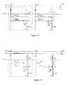
- FIG. 13 shows schematically a circuit in the pre-charging stage of the driving circuit according to the embodiment of the present disclosure.
- the pre-charging control voltage Vselect is the high level
- the light emitting operation voltage Vdd is the low level.
- the fifth TFT 507 and the second TFT 504 are turned off, and the third TFT 505 and the fourth TFT 506 are turned on.
- the voltages at the gate (point A) and the drain (point B) of the first TFT 501 are equal, Vds>Vgs-Vth, where Vds is the source-drain voltage and Vgs is the source-gate voltage.
- the first TFT 501 is in the saturated region, the current Idata is flowed into the first TFT 501 through the fourth TFT 506 , the capacitor 502 stores charges to maintain the source-gate voltage Vgs of the first TFT 501 , and the output current I OLED is equal to Idata at this time.
- FIG. 14 shows schematically a circuit in the light emitting stage of the driving circuit according to the embodiment of the present disclosure.
- the pre-charging control voltage Vselect is the low level
- the light emitting operation voltage Vdd is the high level.
- the third TFT 505 and the fourth TFT 506 are turned off, and the second TFT 504 and the fifth TFT 507 are turned on.
- the voltage at the drain (point B) of the first TFT 501 is the high level.
- the first TFT 501 is still in the saturated region, the output current of the transistor at this time will maintain the value when the transistor enters the saturated region. Therefore, the output current I OLED in the light emitting stage is still Idata in the pre-charging stage, and the output current remains unchanged.
- the output current of the driving circuit shown in FIG. 11 is only related to the input current, and is unrelated with the threshold voltage Vth. Therefore, the effect of the non-uniformity of the threshold voltage on the display is basically eliminated, the output current is stable, and it is easy to realize a high brightness and a high resolution of the display.
- FIG. 15 shows a simulated signal waveform chart of the operation process of the driving circuit in the embodiment of the present disclosure.
- FIG. 15 is a simulation result of the driving circuit shown in FIG. 11 .
- the simulation shows two operation cycles of a single sub pixel. In the first cycle, the pixel is written with the current of 2 uA. In the second cycle, the pixel is written with the current of 3 uA. It can be seen obviously from the waveform chart that the output current I OLED of the pixel follows the change of the input current Idata very well, after the circuit is pre-charged.
- an array substrate comprising the driving circuit provided in the embodiments of the present disclosure.
- a display device comprising the driving circuit provided in the embodiments of the present disclosure.
- the embodiments of the present disclosure provide a pixel circuit, a driving circuit, an array substrate and a display device, which are supplied with the voltage by the light emitting operation voltage Vdd when the pixel circuit enters the light emitting stage, by inputting an inverse signal synchronized with the pre-charging control voltage Vselect at the input terminal of the light emitting operation voltage Vdd to ensure a stable output of the current by the circuit at the light emitting stage. Also, there is no external voltage input terminal which will affect the aperture ratio, thereby increasing the aperture ratio of the OLED employing the current-driven pixel circuit while ensuring the stable output of the current by the current-driven circuit, and thus increasing the lifetime of the OLED employing the current-driven pixel circuit.
Landscapes
- Engineering & Computer Science (AREA)
- Physics & Mathematics (AREA)
- Computer Hardware Design (AREA)
- General Physics & Mathematics (AREA)
- Theoretical Computer Science (AREA)
- Electroluminescent Light Sources (AREA)
- Control Of Indicators Other Than Cathode Ray Tubes (AREA)
Abstract
The present disclosure relates to the OLED display technology. There are provided a pixel circuit, a driving circuit, an array substrate and a display device, which are supplied with the voltage by the light emitting operation voltage when the pixel circuit enters the light emitting stage, by inputting an inverse signal synchronized with the pre-charging control voltage at the input terminal of the light emitting operation voltage to ensure a stable output of the current by the circuit at the light emitting stage. Also, it does not require an arrangement of an external voltage input terminal which will affect the aperture ratio, thereby increasing the aperture ratio of the OLED employing the current-driven pixel circuit while ensuring the stable output of the current by the current-driven circuit, and thus increasing the lifetime of the OLED employing the current-driven pixel circuit.
Description
This application is the National Stage of PCT/CN2013/089155 filed on Dec. 12, 2013, which claims priority under 35 U.S.C. § 119 of Chinese Application No. 201310407319.1 filed on Sept. 9, 2013, the disclosure of which is incorporated by reference.
The present disclosure relates to the technical field of organic light emitting display, and particularly to a pixel circuit, a driving circuit, an array substrate and a display device.
The driving methods for an Organic Light Emitting Display (OLED) pixel circuit may be divided into a current-driven method and a voltage-driven method. FIG. 1 shows a voltage-driven pixel circuit, and FIG. 2 shows a current-driven pixel circuit. In the voltage-driven pixel circuit, the formula for the output current IOLED is as follows:
where μn is a carrier mobility, Cox is a gate oxide capacitance, W/L is a width-to-length ratio of a transistor, Vdata is a data voltage, Voled is an OLED light emitting operation voltage shared by all pixel units, and Vth is a threshold voltage of the transistor. For an enhancement-type Thin Film Transistor (TFT), Vth is a positive value. For a depletion-type TFT, Vth is a negative value. It can be known that if Vth of a pixel varies with time, the output current IOLED of the pixel at different times will be different. The afterimage phenomenon will occur, and a stable display of an Organic Light Emitting Diode (OLED) display temporally cannot be ensured. The advantage of the current-driven method with respect to the voltage-driven method is that the output current IOLED is always equal to the input current Idata. In the current-driven pixel circuit, even if the threshold voltage Vth of the pixel varies with time, the current-driven pixel circuit can adjust autonomously to ensure that the output current IOLED is always equal to the input current Idata, so as to realize a uniform display spatially and a stable display temporally of the OLED. This is because that the operation process of the current-driven pixel circuit may generally be divided into two stages, the first of which is a pre-charging stage, and the second of which is a light emitting stage. At the pre-charging stage, the output current IOLED is equal to the input current Idata, at the same time, charge is stored in a capacitor of the current-driven pixel circuit. At the light emitting stage, since the charge has been stored in the capacitor of the current-driven pixel circuit, it can be ensured that the output current IOLED in the current-driven pixel circuit is still equal to the output current IOLED at the pre-charging stage, i.e., still equal to the input current Idata at the pre-charging stage. A particular current-driven pixel circuit is as shown in FIG. 3 , in the circuit, there is an input terminal of an external control voltage Vctrl for supplying the voltage to the circuit in the light emitting stage, which is connected to a gate of a TFT, and an input terminal of an operation voltage VDD of the circuit is connected to one of a source and a drain of the TFT. A simulated signal waveform chart of the circuit is as shown in FIG. 4 . An inverse signal synchronized with the signal input from the input terminal of a pre-charging control voltage Vselect for supplying the voltage to the circuit in the pre-charging stage is input from the input terminal of the external control voltage Vctrl, to realize a supply of voltage to the driving circuit by the pre-charging control voltage Vselect in the pre-charging stage, and a supply of voltage to the circuit by a voltage combined by the external control voltage Vctrl and the operation voltage VDD through a TFT connected thereto, ensuring the output current IOLED of the current-driven pixel circuit existing in the light emitting stage. However, the existence of the external Vctrl input terminal will decrease the aperture ratio of the pixels. With the decrease of the aperture ratio of the pixels, the lifetime of the OLED is decreased.
There provide a pixel circuit, a driving circuit, an array substrate and a display device in embodiments of the present disclosure to prolong the lifetime of the OLED employing the current-driven pixel circuit.
There is provided a pixel circuit comprising: a first thin film transistor whose gate is connected to an input terminal of a pre-charging control voltage and a current input terminal, and drain is connected to the input terminal of the pre-charging control voltage, the current input terminal and an input terminal of a light emitting operation voltage for inputting an inverse signal synchronized with the pre-charging control voltage; a capacitor whose two ends are connected to a source and the gate of the first thin film transistor, respectively; and an organic light emitting diode whose positive pole is connected to the source of the first thin film transistor, and negative pole is connected to an input terminal of a ground voltage.
Optionally, the drain of the first thin film transistor is connected to the input terminal of the light emitting operation voltage through a diode.
Optionally, the drain of the first thin film transistor is connected to the input terminal of the light emitting operation voltage through a second thin film transistor; a gate and one of a source and a drain of the second thin film transistor are connected to the input terminal of the light emitting operation voltage, and the other one of the source and the drain is connected to the drain of the first thin film transistor.
Optionally, the gate and/or the drain of the first thin film transistor is connected to the input terminal of the pre-charging control voltage and the current input terminal through a thin film transistor operating as a switch.
Optionally, the gate of the first thin film transistor is connected to the input terminal of the pre-charging control voltage and the current input terminal, through a third thin film transistor whose gate is connected to the input terminal of the pre-charging control voltage, one of source and drain is connected to the gate of the first thin film transistor, and the other one of source and drain is connected to the current input terminal; and/or the drain of the first thin film transistor is connected to the input terminal of the pre-charging control voltage and the current input terminal, through a fourth thin film transistor whose gate is connected to the input terminal of the pre-charging control voltage, one of source and drain is connected to the drain of the first thin film transistor, and the other one of source and drain is connected to the current input terminal.
A driving circuit comprises multiple pixel circuits provided in the embodiments of the present disclosure, the multiple pixel circuits provided in the embodiments of the present disclosure being formed in a matrix; wherein the pixel circuits in the same row of the matrix among the multiple pixel circuits provided in the embodiments of the present disclosure are connected to the same input terminal of the light emitting operation voltage, and are connected to the same input terminal of the pre-charging control voltage; and the pixel circuits in the same column of the matrix among the multiple pixel circuits provided in the embodiments of the present disclosure are connected to the same current input terminal.
There is provided an array substrate comprising the driving circuit provided in the embodiments of the present disclosure.
There is provided a display device comprising the driving circuit provided in the embodiments of the present disclosure.
There provide in the embodiments of the present disclosure the pixel circuit, the driving circuit, the array substrate and the display device, which are supplied with the voltage by the light emitting operation voltage when the pixel circuit enters the light emitting stage, by inputting an inverse signal synchronized with the pre-charging control voltage at the input terminal of the light emitting operation voltage to ensure a stable output of the current by the circuit in the light emitting stage. Also, it does not require an arrangement of an external voltage input terminal which will decrease the aperture ratio, thereby increasing the aperture ratio of the OLED employing the current-driven pixel circuit while ensuring the stable output of the current by the current-driven circuit, and thus increasing the lifetime of the OLED employing the current-driven pixel circuit.
There provide in the embodiments of the present disclosure a pixel circuit, a driving circuit, an array substrate and a display device, which are supplied with the voltage by the light emitting operation voltage when the pixel circuit enters the light emitting stage, by inputting an inverse signal synchronized with the pre-charging control voltage Vselect at the input terminal of the light emitting operation voltage. It ensures a stable output of the current by the circuit in the light emitting stage. Also, it does not require an arrangement of an external voltage input terminal which will decrease the aperture ratio, thereby increasing the aperture ratio of the OLED employing the current-driven pixel circuit while ensuring the stable output of the current by the current-driven circuit, and thus increasing the lifetime of the OLED employing the current-driven pixel circuit.
As shown in FIG. 5 , a pixel circuit according to a first embodiment of the present disclosure comprises:
a first thin film transistor (TFT) 501, whose gate is connected to an input terminal of a pre-charging control voltage Vselect and a current input terminal, and drain is connected to the input terminal of the pre-charging control voltage Vselect, the current input terminal and an input terminal of a light emitting operation voltage Vdd for inputting an inverse signal synchronized with the pre-charging control voltage Vselect;
a capacitor 502, having two ends being connected to a source and the gate of the first TFT 501, respectively; and
an organic light emitting diode (LED) 503 whose positive pole is connected to the source of the first TFT 501, and negative pole is connected to an input terminal of a ground voltage Vss.
An inverse signal synchronized with the pre-charging control voltage Vselect is input from the input terminal of the light emitting operation voltage Vdd. Therefore, the circuit is supplied with the voltage by the signal input from the input terminal of the pre-charging control voltage Vselect in the pre-charging stage, and is supplied with the voltage by the signal input from the light emitting operation voltage Vdd in the light emitting stage thereby, it is ensured that there is current output in the circuit in the light emitting stage, while the capacitor 502 ensures that the current output in the light emitting stage is the same as that in the pre-charging stage. There is no external signal terminal in the circuit which will affect the aperture ratio, thereby increasing the aperture ratio of the OLED employing the current-driven pixel circuit, and thus increasing the lifetime of the OLED employing the current-driven pixel circuit.
In the practical application, the drain voltages of the first TFTs 501 of the adjacent pixels will be different when the currents input from the current input terminals of the adjacent pixels in the same row are different, which easily results in the direction of the current in the driving circuit for a pixel with a higher drain voltage is opposite to the direction of the current required in a normal operation, thereby affecting a normal display of the OLED. Therefore, in order to prevent the direction of the current in the driving circuits for the respective pixels from being opposite to the direction of the current required in the normal operation, the drain of the first TFT 501 in the pixel circuit can be connected to the input terminal of the light emitting operation voltage Vdd through a diode to ensure that the current of the driving circuit in the light emitting stage is flowed to the drain of the first TFT 501 from the input terminal of the driving voltage.
Alternatively, for convenience of the manufacture of the OLED, the diode connecting the drain of the first TFT 501 and the input terminal of the light emitting operation voltage Vdd can be replaced with a TFT.
A gate and one of a source and a drain of the second TFT 504 are connected to the input terminal of the light emitting operation voltage Vdd, and the other one of the source and the drain is connected to the drain of the first TFT 501.
The second TFT 504 in FIG. 6 may be viewed as a diode with a positive pole connected to the input terminal of the light emitting operation voltage Vdd and a negative pole connected to the drain of the first TFT 501, thereby ensuring that the direction of the current in the driving circuit is from the input terminal of the light emitting operation voltage Vdd to the drain of the first TFT 501.
Of course, those skilled in the art may employ other feasible ways to prevent the currents input from the current input terminals of the adjacent pixels in the same row from being different and thus affecting the normal display of the OLED. The implementation provided herein is only exemplary and the other implementations will not be described in detail one by one.
Further, if it needs to progressively drive the driving circuit for the respective pixels, that is, a pre-charging to a next row can only be done after the pre-charging to a previous row is completed, the embodiment of the present disclosure can further provide an alternative way to achieve the progressive driving. That is, the gate and/or the drain of the first TFT 501 can be connected to the input terminal of the pre-charging control voltage Vselect and the current input terminal through a TFT operating as a switch. The TFT operating as the switch is turned on at a high level and is turned off at a low level. Therefore, different signals are input from the input terminal of the pre-charging control voltage Vselect of the respective rows of the pixel circuits to realize the progressive driving.
Specifically, the gate of the first TFT 501 can be connected to the input terminal of the pre-charging control voltage Vselect and the current input terminal through a TFT operating as a switch.
More specifically, the gate of the first TFT 501 is connected to the input terminal of the pre-charging control voltage Vs elect and the current input terminal through a third TFT 505. The gate of the third TFT 505 is connected to the input terminal of the pre-charging control voltage Vselect, one of a source and a drain thereof is connected to the gate of the first TFT 501, and the other one of the source and the drain is connected to the current input terminal.
Further, the drain of the first TFT 501 may also be connected to the input terminal of the pre-charging control voltage Vselect and the current input terminal through a TFT operating as a switch.
More specifically, the drain of the first TFT is connected to the input terminal of the pre-charging control voltage Vselect and the current input terminal through a fourth TFT 506. A gate of the fourth TFT 506 is connected to the input terminal of the pre-charging control voltage Vselect, one of a source and a drain is connected to the drain of the first TFT 501, and the other one of the source and the drain is connected to the current input terminal.
Of course, those skilled in the art may also employ other feasible ways to achieve the progressive driving for the pixel circuits. The implementation provided here is only exemplary, and the other implementations will not be described in detail one by one.
Herein two ends of the capacitor 502 are connected to a source and a gate of the first TFT 501, respectively.
A positive pole of the OLED 503 is connected to the source of the first TFT 501, and the negative pole of the OLED 503 is connected to an input terminal of a ground voltage Vss.
A gate and one of a source and a drain of the second TFT 504 are connected to an input terminal of a light emitting operation voltage Vdd, and the other one of the source and the drain is connected to a drain of the first TFT 501.
A gate of the third TFT 505 is connected to an input terminal of a pre-charging control voltage Vselect, one of a source and a drain of the third TFT 505 is connected to the gate of the first TFT 501, and the other one of the source and the drain is connected to the current input terminal.
A gate of the fourth TFT 506 is connected to the input terminal of the pre-charging control voltage Vselect, one of a source and a drain of the fourth TFT 506 is connected to the drain of the first TFT 501, and the other one of the source and the drain is connected to the current input terminal.
Here, an inverse signal synchronized with the pre-charging control voltage Vselect is input from the input terminal of the light emitting operation voltage Vdd. The circuit is supplied with the voltage by the pre-charging control voltage Vselect when the pixel circuit enters the pre-charging stage, and is supplied with the voltage by the light emitting operation voltage Vdd when the pixel circuit enters the light emitting stage to ensure the current output of the circuit at the pre-charging stage and the light emitting stage. Also, there is no external voltage input terminal which will affect the aperture ratio, thereby increasing the aperture ratio of the OLED employing the current-driven pixel circuit, and further increasing the lifetime of the OLED employing the current-driven pixel circuit. The second TFT 504 may be viewed as a diode with a positive pole being connected to the input terminal of the light emitting operation voltage Vdd and a negative pole being connected to the drain of the first TFT 501, thereby ensuring that the direction of the current in the driving circuit is from the input terminal of the light emitting operation voltage Vdd to the drain of the first TFT 501. The third TFT 505 and the fourth TFT 506 are TFTs operating as switch, which are turned on at the high level and turned off at the low level, thereby inputting different signals by the input terminal of the pre-charging control voltage Vselect of the respective rows of the pixel circuits, so as to achieve the progressive driving.
There further provides in the embodiment of the present disclosure a driving circuit comprising multiple pixel circuits provided in the embodiments of the present disclosure being formed in a matrix.
The pixel circuits in the same row of the matrix among the multiple pixel circuits provided in the embodiments of the present disclosure are connected to the same input terminal of the light emitting operation voltage, and are connected to the same input terminal of the pre-charging control voltage.
The pixel circuits in the same column of the matrix among the multiple pixel circuits provided in the embodiments of the present disclosure are connected to the same current input terminal.
A source and a drain of the fifth TFT 507 are connected to the input terminal of the light emitting operation voltage Vdd and an input terminal of an operation voltage VDD respectively, a gate of the fifth TFT 507 is connected to a signal input terminal Input for inputting an inverse signal synchronized with the pre-charging control voltage Vselect, and the fifth TFT 507 is a N-type TFT.
The fifth TFT 507 is arranged in the pixel circuits in the first column of the matrix among the multiple pixel circuits provided in the embodiment of the present disclosure. By inputting an inverse signal synchronized with the pre-charging control voltage Vselect at the gate of the fifth TFT 507 and connecting the input terminal of the light emitting operation voltage Vdd and the input terminal of the operation voltage VDD at the source and the drain thereof respectively, the signal output from one of the source and the drain of the fifth TFT 507 which is connected to the input terminal of the light emitting operation voltage Vdd is the signal input to the pixel circuits from the input terminal of the light emitting operation voltage Vdd. After the signal is input from the input terminal of the operation voltage VDD and the input terminal of the pre-charging control voltage Vselect, signal output from the one of the source and the drain of the fifth TFT 507 which is connected to the input terminal of the light emitting operation voltage Vdd is the inverse signal synchronized with the pre-charging control voltage Vselect, thereby ensuring that the signal input to the pixel circuits from the input terminal of the light emitting operation voltage Vdd is the inverse signal synchronized with the pre-charging control voltage Vselect.
Of course, those skilled in the art may employ other feasible ways to ensure that the signal input to the pixel circuits from the input terminal of the light emitting operation voltage Vdd is the inverse signal synchronized with the pre-charging control voltage Vselect. The implementation provided here is only exemplary, and the other implementations will not be described in detail one by one.
The pixel circuit comprises: a first TFT 501, a second TFT 504, a third TFT 505, a fourth TFT 506 and a fifth TFT 507, and further comprises a capacitor 502 and a OLED 503.
Two ends of the capacitor 502 are connected to a source and a gate of the first TFT 501, respectively.
A positive pole of the OLED 503 is connected to the source of the first TFT 501, and the negative pole of the OLED 503 is connected to an input terminal of a ground voltage Vss.
A gate and one of a source and a drain of the second TFT 504 are connected to an input terminal of a light emitting operation voltage Vdd, and the other one of the source and the drain is connected to a drain of the first TFT 501.
A gate of the third TFT 505 is connected to an input terminal of a pre-charging control voltage Vselect, one of a source and a drain of the third TFT 505 is connected to the gate of the first TFT 501, and the other one of the source and the drain is connected to the current input terminal.
A gate of the fourth TFT 506 is connected to the input terminal of the pre-charging control voltage Vselect, one of a source and a drain of the fourth TFT 506 is connected to the drain of the first TFT 501, and the other one of the source and the drain is connected to the current input terminal.
A source and a drain of the fifth TFT 507 in the pixel circuits of the first column of the matrix among the multiple pixel circuits are connected respectively to the input terminal of the light emitting operation voltage Vdd and an input terminal of an operation voltage VDD. A gate of the fifth TFT 507 is connected to a signal input terminal Input for inputting an inverse signal synchronized with the pre-charging control voltage Vselect, and the fifth TFT 507 is a N-type TFT. Exemplarily, as shown in FIG. 12 , the signal input from the input terminal of the operation voltage VDD may also be opposite to the signal input from the input terminal of the pre-charging control voltage Vselect.
The pixel circuits in the same row of the matrix among the multiple pixel circuits are connected to the same input terminal of the light emitting operation voltage, and are connected to the same input terminal of the pre-charging control voltage.
The pixel circuits in the same column of the matrix among the multiple pixel circuits are connected to the same current input terminal.
In the following, the operation principle of the driving circuit shown in FIG. 11 will be described by way of example in detail.
It can be known that the output current of the driving circuit shown in FIG. 11 is only related to the input current, and is unrelated with the threshold voltage Vth. Therefore, the effect of the non-uniformity of the threshold voltage on the display is basically eliminated, the output current is stable, and it is easy to realize a high brightness and a high resolution of the display.
There is further provided in the embodiment of the present disclosure an array substrate comprising the driving circuit provided in the embodiments of the present disclosure.
There is provided in the embodiment of the present disclosure a display device comprising the driving circuit provided in the embodiments of the present disclosure.
The embodiments of the present disclosure provide a pixel circuit, a driving circuit, an array substrate and a display device, which are supplied with the voltage by the light emitting operation voltage Vdd when the pixel circuit enters the light emitting stage, by inputting an inverse signal synchronized with the pre-charging control voltage Vselect at the input terminal of the light emitting operation voltage Vdd to ensure a stable output of the current by the circuit at the light emitting stage. Also, there is no external voltage input terminal which will affect the aperture ratio, thereby increasing the aperture ratio of the OLED employing the current-driven pixel circuit while ensuring the stable output of the current by the current-driven circuit, and thus increasing the lifetime of the OLED employing the current-driven pixel circuit.
Obviously, those skilled in the art can make modifications and variations to the embodiments of the present disclosure without departing from the spirit and the scope of the present disclosure. Hence, it is intended to include these modifications and variations in the present disclosure as long as these modifications and variations belong to the scope of the claims of the present disclosure and the equivalents thereto.
Claims (16)
1. A pixel circuit, comprising:
at least one of a gate and a drain of a first thin film transistor being directly connected to both an input terminal of a pre-charging control voltage and a current input terminal;
a second thin film transistor whose gate is directly connected to one of a source and a drain thereof, wherein
the gate and said one of the source and the drain of the second thin film transistor are both connected to an input terminal of a light emitting operation voltage for inputting a light emitting operation voltage synchronized with and inverted compared to the pre-charging control voltage, and the other one of the source and the drain of the second thin film transistor is connected to the drain of the first thin film transistor;
a capacitor whose two ends are connected to a source and the gate of the first thin film transistor, respectively; and
an organic light emitting diode whose positive pole is connected to the source of the first thin film transistor, and negative pole is connected to an input terminal of a ground voltage, wherein one end of the capacitor and the positive pole of the organic light emitting diode are directly connected.
2. The circuit of claim 1 , wherein when the drain of the first thin film transistor is directly connected to the input terminal of the pre-charging control voltage and the current input terminal, the gate of the first thin film transistor is connected to the input terminal of the pre-charging control voltage and the current input terminal through a thin film transistor operating as a switch.
3. The circuit of claim 2 , wherein the gate of the first thin film transistor is connected to the input terminal of the pre-charging control voltage and the current input terminal, through a third thin film transistor whose gate is connected to the input terminal of the pre-charging control voltage, one of source and drain is connected to the gate of the first thin film transistor, and the other one of source and drain is connected to the current input terminal.
4. The circuit of claim 3 , wherein the input terminal of the pre-charging control voltage is directly connected to the current input terminal.
5. The circuit of claim 1 , wherein when the gate of the first thin film transistor is directly connected to the input terminal of the pre-charging control voltage and the current input terminal, the drain of the first thin film transistor is connected to the input terminal of the pre-charging control voltage and the current input terminal through a thin film transistor operating as a switch.
6. The circuit of claim 5 , wherein the drain of the first thin film transistor is connected to the input terminal of the pre-charging control voltage and the current input terminal, through a fourth thin film transistor whose gate is connected to the input terminal of the pre-charging control voltage, one of source and drain is connected to the drain of the first thin film transistor, and the other one of source and drain is connected to the current input terminal.
7. The circuit of claim 6 , wherein the other end of the capacitor is directly connected to the input terminal of the pre-charging control voltage and the current input terminal.
8. A driving circuit comprising multiple pixel circuits of claim 1 formed in a matrix;
wherein the pixel circuits in the same row of the matrix among the multiple pixel circuits are connected to the same input terminal of the light emitting operation voltage, and are connected to the same input terminal of the pre-charging control voltage; and the pixel circuits in the same column of the matrix among the multiple pixel circuits are connected to the same current input terminal.
9. The driving circuit of claim 8 , wherein the pixel circuits in a first column of the matrix among the multiple pixel circuits of claim 1 comprise a fifth thin film transistor;
a source and a drain of the fifth thin film transistor are connected to the input terminal of the light emitting operation voltage and an input terminal of an operation voltage respectively, and a gate thereof is connected to a signal input terminal for inputting an inverse signal synchronized with the pre-charging control voltage, and the fifth thin film transistor is a N-type thin film transistor.
10. An array substrate comprising the driving circuit of claim 8 .
11. The array substrate of claim 10 , wherein the pixel circuits in a first column of the matrix among the multiple pixel circuits comprise a fifth thin film transistor;
a source and a drain of the fifth thin film transistor are connected to the input terminal of the light emitting operation voltage and an input terminal of an operation voltage respectively, and a gate thereof is connected to a signal input terminal for inputting an inverse signal synchronized with the pre-charging control voltage, and the fifth thin film transistor is a N-type thin film transistor.
12. The driving circuit of claim 8 , wherein when the drain of the first thin film transistor is directly connected to the input terminal of the pre-charging control voltage and the current input terminal, the gate of the first thin film transistor is connected to the input terminal of the pre-charging control voltage and the current input terminal through a thin film transistor operating as a switch.
13. The driving circuit of claim 12 , wherein the gate of the first thin film transistor is connected to the input terminal of the pre-charging control voltage and the current input terminal, through a third thin film transistor whose gate is connected to the input terminal of the pre-charging control voltage, one of source and drain is connected to the gate of the first thin film transistor, and the other one of source and drain is connected to the current input terminal.
14. The driving circuit of claim 8 , wherein when the gate of the first thin film transistor is directly connected to the input terminal of the pre-charging control voltage and the current input terminal, the drain of the first thin film transistor is connected to the input terminal of the pre-charging control voltage and the current input terminal through a thin film transistor operating as a switch.
15. The driving circuit of claim 14 , wherein the drain of the first thin film transistor is connected to the input terminal of the pre-charging control voltage and the current input terminal, through a fourth thin film transistor whose gate is connected to the input terminal of the pre-charging control voltage, one of source and drain is connected to the drain of the first thin film transistor, and the other one of source and drain is connected to the current input terminal.
16. The circuit of claim 1 , wherein when both the gate and the drain of the first thin film transistor are directly connected to the input terminal of the pre-charging control voltage and the current input terminal, the other end of the capacitor is directly connected to the input terminal of the pre-charging control voltage and the current input terminal, and the input terminal of the pre-charging control voltage is directly connected to the current input terminal.
Applications Claiming Priority (4)
| Application Number | Priority Date | Filing Date | Title |
|---|---|---|---|
| CN201310407319.1 | 2013-09-09 | ||
| CN201310407319.1A CN103474028B (en) | 2013-09-09 | 2013-09-09 | Pixel circuit, drive circuit, array substrate and display device |
| CN201310407319 | 2013-09-09 | ||
| PCT/CN2013/089155 WO2015032145A1 (en) | 2013-09-09 | 2013-12-12 | Pixel circuit, drive circuit, array substrate and display device |
Publications (2)
| Publication Number | Publication Date |
|---|---|
| US20160163263A1 US20160163263A1 (en) | 2016-06-09 |
| US10276097B2 true US10276097B2 (en) | 2019-04-30 |
Family
ID=49798852
Family Applications (1)
| Application Number | Title | Priority Date | Filing Date |
|---|---|---|---|
| US14/366,865 Active 2034-09-14 US10276097B2 (en) | 2013-09-09 | 2013-12-12 | Pixel circuit, driving circuit, array substrate and display device |
Country Status (3)
| Country | Link |
|---|---|
| US (1) | US10276097B2 (en) |
| CN (1) | CN103474028B (en) |
| WO (1) | WO2015032145A1 (en) |
Families Citing this family (5)
| Publication number | Priority date | Publication date | Assignee | Title |
|---|---|---|---|---|
| US10762843B2 (en) * | 2018-03-28 | 2020-09-01 | Sharp Kabushiki Kaisha | Pixel circuit using direct charging and that performs light-emitting device compensation |
| KR102541942B1 (en) * | 2018-09-28 | 2023-06-09 | 엘지디스플레이 주식회사 | Current Sensing Device And Organic Light Emitting Display Device Including The Same |
| CN109461386A (en) * | 2019-01-04 | 2019-03-12 | 京东方科技集团股份有限公司 | Display device |
| CN111833815B (en) * | 2020-07-31 | 2022-05-31 | 合肥京东方卓印科技有限公司 | Pixel driving circuit and method, display panel and driving method |
| CN115188314B (en) * | 2022-09-08 | 2023-01-31 | 惠科股份有限公司 | Display circuit and display device of dysmorphism screen |
Citations (18)
| Publication number | Priority date | Publication date | Assignee | Title |
|---|---|---|---|---|
| US20040150593A1 (en) | 2003-01-31 | 2004-08-05 | Wen-Cheng Yen | Active matrix LED display driving circuit |
| CN1584963A (en) | 2003-08-21 | 2005-02-23 | 精工爱普生株式会社 | Electro-optical device and electronic apparatus |
| US20060022605A1 (en) | 2004-07-29 | 2006-02-02 | Lg Philips Lcd Co., Ltd. | Driving current of organic light emitting display and method of driving the same |
| US20060066254A1 (en) * | 2004-09-30 | 2006-03-30 | Akifumi Sasaki | Organic EL pixel circuit |
| US20060139264A1 (en) * | 2004-12-24 | 2006-06-29 | Choi Sang M | Data driver and light emitting diode display device including the same |
| US20070126680A1 (en) * | 2005-12-02 | 2007-06-07 | Samsung Electronics Co., Ltd | Display device and method for driving the same |
| US20070182671A1 (en) * | 2003-09-23 | 2007-08-09 | Arokia Nathan | Pixel driver circuit |
| CN101097681A (en) | 2006-06-27 | 2008-01-02 | Lg.菲利浦Lcd株式会社 | Organic electroluminescent display device and driving method of the same |
| US20080297056A1 (en) * | 2007-05-30 | 2008-12-04 | Canon Kabushiki Kaisha | Light emitting element circuit and drive method thereof |
| CN101577085A (en) | 2008-05-08 | 2009-11-11 | 索尼株式会社 | Display apparatus, display-apparatus driving method and electronic instrument |
| US20100053041A1 (en) | 2008-09-03 | 2010-03-04 | Canon Kabushiki Kaisha | Pixel circuit, light emitting display device and driving method thereof |
| US20100225770A1 (en) | 2009-03-05 | 2010-09-09 | Casio Computer Co., Ltd. | Drive circuit array substrate and production and test methods thereof |
| CN102646386A (en) | 2011-05-13 | 2012-08-22 | 京东方科技集团股份有限公司 | Pixel unit circuit, pixel array, panel and panel driving method |
| US8314756B2 (en) * | 2007-11-02 | 2012-11-20 | Cambridge Display Technology Limited | Pixel driver circuits comprising a thin film transistor with a floating gate |
| CN203520833U (en) | 2013-09-09 | 2014-04-02 | 京东方科技集团股份有限公司 | Pixel circuit, driving circuit, array substrate and display device |
| US8760374B2 (en) * | 2004-05-21 | 2014-06-24 | Semiconductor Energy Laboratory Co., Ltd. | Display device having a light emitting element |
| US8791887B2 (en) * | 2008-08-15 | 2014-07-29 | Cambridge Display Technology Limited | Method of compensating for capacitance of a programming line of an OLED display |
| US20140320555A1 (en) * | 2013-04-25 | 2014-10-30 | Internatiional Business Machines Corporation | Active matrix triode switch driver circuit |
Family Cites Families (1)
| Publication number | Priority date | Publication date | Assignee | Title |
|---|---|---|---|---|
| JP2007021503A (en) * | 2005-07-12 | 2007-02-01 | Fanuc Ltd | Laser beam machine |
-
2013
- 2013-09-09 CN CN201310407319.1A patent/CN103474028B/en active Active
- 2013-12-12 US US14/366,865 patent/US10276097B2/en active Active
- 2013-12-12 WO PCT/CN2013/089155 patent/WO2015032145A1/en active Application Filing
Patent Citations (23)
| Publication number | Priority date | Publication date | Assignee | Title |
|---|---|---|---|---|
| US20040150593A1 (en) | 2003-01-31 | 2004-08-05 | Wen-Cheng Yen | Active matrix LED display driving circuit |
| CN1584963A (en) | 2003-08-21 | 2005-02-23 | 精工爱普生株式会社 | Electro-optical device and electronic apparatus |
| US7417607B2 (en) | 2003-08-21 | 2008-08-26 | Seiko Epson Corporation | Electro-optical device and electronic apparatus |
| US20070182671A1 (en) * | 2003-09-23 | 2007-08-09 | Arokia Nathan | Pixel driver circuit |
| US8760374B2 (en) * | 2004-05-21 | 2014-06-24 | Semiconductor Energy Laboratory Co., Ltd. | Display device having a light emitting element |
| US20060022605A1 (en) | 2004-07-29 | 2006-02-02 | Lg Philips Lcd Co., Ltd. | Driving current of organic light emitting display and method of driving the same |
| US20060066254A1 (en) * | 2004-09-30 | 2006-03-30 | Akifumi Sasaki | Organic EL pixel circuit |
| US20060139264A1 (en) * | 2004-12-24 | 2006-06-29 | Choi Sang M | Data driver and light emitting diode display device including the same |
| US20070126680A1 (en) * | 2005-12-02 | 2007-06-07 | Samsung Electronics Co., Ltd | Display device and method for driving the same |
| CN101097681A (en) | 2006-06-27 | 2008-01-02 | Lg.菲利浦Lcd株式会社 | Organic electroluminescent display device and driving method of the same |
| US8284124B2 (en) | 2006-06-27 | 2012-10-09 | Lg Display Co., Ltd. | Organic electroluminescent display device and driving method of the same |
| US20080297056A1 (en) * | 2007-05-30 | 2008-12-04 | Canon Kabushiki Kaisha | Light emitting element circuit and drive method thereof |
| US8314756B2 (en) * | 2007-11-02 | 2012-11-20 | Cambridge Display Technology Limited | Pixel driver circuits comprising a thin film transistor with a floating gate |
| CN101577085A (en) | 2008-05-08 | 2009-11-11 | 索尼株式会社 | Display apparatus, display-apparatus driving method and electronic instrument |
| US20090278834A1 (en) | 2008-05-08 | 2009-11-12 | Sony Corporation | Display apparatus, display-apparatus driving method and electronic instrument |
| US8791887B2 (en) * | 2008-08-15 | 2014-07-29 | Cambridge Display Technology Limited | Method of compensating for capacitance of a programming line of an OLED display |
| CN101667391A (en) | 2008-09-03 | 2010-03-10 | 佳能株式会社 | Pixel circuit, light emitting display device and driving method thereof |
| US20100053041A1 (en) | 2008-09-03 | 2010-03-04 | Canon Kabushiki Kaisha | Pixel circuit, light emitting display device and driving method thereof |
| US20100225770A1 (en) | 2009-03-05 | 2010-09-09 | Casio Computer Co., Ltd. | Drive circuit array substrate and production and test methods thereof |
| CN102646386A (en) | 2011-05-13 | 2012-08-22 | 京东方科技集团股份有限公司 | Pixel unit circuit, pixel array, panel and panel driving method |
| US20120287103A1 (en) | 2011-05-13 | 2012-11-15 | Boe Technology Group Co., Ltd. | Pixel unit circuit, pixel array, display panel and display panel driving method |
| US20140320555A1 (en) * | 2013-04-25 | 2014-10-30 | Internatiional Business Machines Corporation | Active matrix triode switch driver circuit |
| CN203520833U (en) | 2013-09-09 | 2014-04-02 | 京东方科技集团股份有限公司 | Pixel circuit, driving circuit, array substrate and display device |
Non-Patent Citations (6)
| Title |
|---|
| Chinese Office Action of Chinese Application No. 201310407319.1 with English translation, dated Jul. 21, 2014. |
| English translation of the International Preliminary Report on Patentability and Written Opinion of the International Searching Authority of PCT/CN2013/089155, dated Mar. 15, 2016. |
| English Translation of the International Search Report of PCT/CN2013/089155 published in English dated Mar. 12, 2015. |
| International Search Report, International Preliminary Report on Patentability and Written Opinion of the International Searching Authority of PCT/CN2013/089155 in Chinese, dated Jun. 4, 2014. |
| Patent Grant Notification for the priority application CN 201310407319.1 filed on Sep. 9, 2013 which issued as Chinese Patent 2014101500454800 dated Oct. 31, 2014 in Chinese. |
| Patent Grant Notification for the priority application CN 201310407319.1 filed on Sep. 9, 2013 which issued as Chinese Patent 2014101500454800 dated Oct. 31, 2014 in English. |
Also Published As
| Publication number | Publication date |
|---|---|
| CN103474028A (en) | 2013-12-25 |
| WO2015032145A1 (en) | 2015-03-12 |
| US20160163263A1 (en) | 2016-06-09 |
| CN103474028B (en) | 2014-12-10 |
Similar Documents
| Publication | Publication Date | Title |
|---|---|---|
| CN110223636B (en) | Pixel driving circuit, driving method thereof and display device | |
| US10242625B2 (en) | Pixel driving circuit, pixel driving method and display apparatus | |
| US10607538B2 (en) | Pixel circuit, pixel, AMOLED display device comprising same and driving method thereof | |
| US10621916B2 (en) | Driving circuit and driving method thereof, and display device | |
| US10032415B2 (en) | Pixel circuit and driving method thereof, display device | |
| US9852685B2 (en) | Pixel circuit and driving method thereof, display apparatus | |
| US9508287B2 (en) | Pixel circuit and driving method thereof, display apparatus | |
| CN106847183B (en) | Driving circuit of active matrix organic light emitting diode with hybrid transistor | |
| US20170186782A1 (en) | Pixel circuit of active-matrix light-emitting diode and display panel having the same | |
| US9355595B2 (en) | Pixel unit driving circuit having an erasing transistor and matching transistor, and method thereof | |
| US9548024B2 (en) | Pixel driving circuit, driving method thereof and display apparatus | |
| US10283042B2 (en) | Pixel driving circuit, pixel driving method, and display device | |
| EP2775474B1 (en) | Amoled drive compensation circuit and method and display device thereof | |
| CN108074529A (en) | Pixel circuit in electroluminescent display | |
| US20160284273A1 (en) | Pixel Circuit, Driving Method Thereof and Display Apparatus | |
| US10726790B2 (en) | OLED pixel circuit and method for driving the same, display apparatus | |
| WO2016023311A1 (en) | Pixel drive circuit, pixel drive method and display apparatus | |
| CN109166522B (en) | Pixel circuit, driving method thereof and display device | |
| US10157576B2 (en) | Pixel driving circuit, driving method for same, and display apparatus | |
| CN107369412B (en) | Pixel circuit, driving method thereof and display device | |
| US10276097B2 (en) | Pixel circuit, driving circuit, array substrate and display device | |
| US20210193046A1 (en) | Pixel unit, display panel and electronic device | |
| WO2021007694A1 (en) | Pixel unit, array substrate, and display terminal | |
| TW201721623A (en) | Driving circuit of active-matrix organic light-emitting diode with hybrid transistors | |
| CN109410835B (en) | Novel OLED drive circuit |
Legal Events
| Date | Code | Title | Description |
|---|---|---|---|
| AS | Assignment |
Owner name: BOE TECHNOLOGY GROUP CO., LTD., CHINA Free format text: ASSIGNMENT OF ASSIGNORS INTEREST;ASSIGNORS:DUAN, LIYE;WANG, LIRONG;WU, ZHONGYUAN;REEL/FRAME:033141/0069 Effective date: 20140423 |
|
| STPP | Information on status: patent application and granting procedure in general |
Free format text: PUBLICATIONS -- ISSUE FEE PAYMENT VERIFIED |
|
| STCF | Information on status: patent grant |
Free format text: PATENTED CASE |
|
| MAFP | Maintenance fee payment |
Free format text: PAYMENT OF MAINTENANCE FEE, 4TH YEAR, LARGE ENTITY (ORIGINAL EVENT CODE: M1551); ENTITY STATUS OF PATENT OWNER: LARGE ENTITY Year of fee payment: 4 |