US10270052B2 - Electronic device - Google Patents
Electronic device Download PDFInfo
- Publication number
- US10270052B2 US10270052B2 US15/870,165 US201815870165A US10270052B2 US 10270052 B2 US10270052 B2 US 10270052B2 US 201815870165 A US201815870165 A US 201815870165A US 10270052 B2 US10270052 B2 US 10270052B2
- Authority
- US
- United States
- Prior art keywords
- hole
- atoms
- transport layer
- transport
- electronic device
- Prior art date
- Legal status (The legal status is an assumption and is not a legal conclusion. Google has not performed a legal analysis and makes no representation as to the accuracy of the status listed.)
- Active
Links
- 230000005525 hole transport Effects 0.000 claims abstract description 203
- 239000000463 material Substances 0.000 claims description 93
- 150000001875 compounds Chemical class 0.000 claims description 82
- 125000003118 aryl group Chemical group 0.000 claims description 75
- 239000002019 doping agent Substances 0.000 claims description 48
- 239000011159 matrix material Substances 0.000 claims description 48
- 125000004432 carbon atom Chemical group C* 0.000 claims description 36
- -1 aromatic hydrocarbon radical Chemical class 0.000 claims description 33
- 150000003254 radicals Chemical class 0.000 claims description 33
- 229910052799 carbon Inorganic materials 0.000 claims description 24
- 229910052760 oxygen Inorganic materials 0.000 claims description 21
- 229910052717 sulfur Inorganic materials 0.000 claims description 20
- 125000004435 hydrogen atom Chemical group [H]* 0.000 claims description 16
- 125000003342 alkenyl group Chemical group 0.000 claims description 15
- 125000003545 alkoxy group Chemical group 0.000 claims description 15
- 125000000304 alkynyl group Chemical group 0.000 claims description 15
- 229910052739 hydrogen Inorganic materials 0.000 claims description 15
- 125000005309 thioalkoxy group Chemical group 0.000 claims description 12
- GVEPBJHOBDJJJI-UHFFFAOYSA-N fluoranthene Chemical compound C1=CC(C2=CC=CC=C22)=C3C2=CC=CC3=C1 GVEPBJHOBDJJJI-UHFFFAOYSA-N 0.000 claims description 11
- UHOVQNZJYSORNB-UHFFFAOYSA-N monobenzene Natural products C1=CC=CC=C1 UHOVQNZJYSORNB-UHFFFAOYSA-N 0.000 claims description 11
- UFWIBTONFRDIAS-UHFFFAOYSA-N Naphthalene Chemical compound C1=CC=CC2=CC=CC=C21 UFWIBTONFRDIAS-UHFFFAOYSA-N 0.000 claims description 10
- 125000006165 cyclic alkyl group Chemical group 0.000 claims description 10
- 125000000217 alkyl group Chemical group 0.000 claims description 9
- YNPNZTXNASCQKK-UHFFFAOYSA-N phenanthrene Chemical compound C1=CC=C2C3=CC=CC=C3C=CC2=C1 YNPNZTXNASCQKK-UHFFFAOYSA-N 0.000 claims description 8
- 229910052710 silicon Inorganic materials 0.000 claims description 8
- 125000001424 substituent group Chemical group 0.000 claims description 8
- 125000000520 N-substituted aminocarbonyl group Chemical group [*]NC(=O)* 0.000 claims description 6
- ZUOUZKKEUPVFJK-UHFFFAOYSA-N diphenyl Chemical compound C1=CC=CC=C1C1=CC=CC=C1 ZUOUZKKEUPVFJK-UHFFFAOYSA-N 0.000 claims description 6
- XSXHWVKGUXMUQE-UHFFFAOYSA-N osmium dioxide Inorganic materials O=[Os]=O XSXHWVKGUXMUQE-UHFFFAOYSA-N 0.000 claims description 6
- 229910052723 transition metal Inorganic materials 0.000 claims description 6
- 150000003624 transition metals Chemical class 0.000 claims description 6
- 125000001931 aliphatic group Chemical group 0.000 claims description 5
- 229910044991 metal oxide Inorganic materials 0.000 claims description 5
- 150000004706 metal oxides Chemical class 0.000 claims description 5
- 229910052711 selenium Inorganic materials 0.000 claims description 4
- YJTKZCDBKVTVBY-UHFFFAOYSA-N 1,3-Diphenylbenzene Chemical group C1=CC=CC=C1C1=CC=CC(C=2C=CC=CC=2)=C1 YJTKZCDBKVTVBY-UHFFFAOYSA-N 0.000 claims description 3
- 239000004215 Carbon black (E152) Substances 0.000 claims description 3
- 235000010290 biphenyl Nutrition 0.000 claims description 3
- 239000004305 biphenyl Substances 0.000 claims description 3
- 239000002537 cosmetic Substances 0.000 claims description 3
- 229930195733 hydrocarbon Natural products 0.000 claims description 3
- 229910001507 metal halide Inorganic materials 0.000 claims description 3
- 150000005309 metal halides Chemical class 0.000 claims description 3
- NRNFFDZCBYOZJY-UHFFFAOYSA-N p-quinodimethane Chemical group C=C1C=CC(=C)C=C1 NRNFFDZCBYOZJY-UHFFFAOYSA-N 0.000 claims description 3
- 229910000314 transition metal oxide Inorganic materials 0.000 claims description 3
- ICPSWZFVWAPUKF-UHFFFAOYSA-N 1,1'-spirobi[fluorene] Chemical compound C1=CC=C2C=C3C4(C=5C(C6=CC=CC=C6C=5)=CC=C4)C=CC=C3C2=C1 ICPSWZFVWAPUKF-UHFFFAOYSA-N 0.000 claims description 2
- 125000002529 biphenylenyl group Chemical group C1(=CC=CC=2C3=CC=CC=C3C12)* 0.000 claims description 2
- RMBPEFMHABBEKP-UHFFFAOYSA-N fluorene Chemical compound C1=CC=C2C3=C[CH]C=CC3=CC2=C1 RMBPEFMHABBEKP-UHFFFAOYSA-N 0.000 claims description 2
- NIHNNTQXNPWCJQ-UHFFFAOYSA-N o-biphenylenemethane Natural products C1=CC=C2CC3=CC=CC=C3C2=C1 NIHNNTQXNPWCJQ-UHFFFAOYSA-N 0.000 claims description 2
- 125000006836 terphenylene group Chemical group 0.000 claims description 2
- 150000001338 aliphatic hydrocarbons Chemical class 0.000 claims 3
- 125000001997 phenyl group Chemical group [H]C1=C([H])C([H])=C(*)C([H])=C1[H] 0.000 claims 1
- 239000010410 layer Substances 0.000 description 179
- 101100489923 Saccharomyces cerevisiae (strain ATCC 204508 / S288c) ABF2 gene Proteins 0.000 description 44
- 101150096395 him-1 gene Proteins 0.000 description 44
- IXHWGNYCZPISET-UHFFFAOYSA-N 2-[4-(dicyanomethylidene)-2,3,5,6-tetrafluorocyclohexa-2,5-dien-1-ylidene]propanedinitrile Chemical compound FC1=C(F)C(=C(C#N)C#N)C(F)=C(F)C1=C(C#N)C#N IXHWGNYCZPISET-UHFFFAOYSA-N 0.000 description 38
- 101100275159 Arabidopsis thaliana COBL7 gene Proteins 0.000 description 21
- 101100180341 Arabidopsis thaliana IWS1 gene Proteins 0.000 description 21
- 101150005224 SBH1 gene Proteins 0.000 description 21
- 101100256357 Schizosaccharomyces pombe (strain 972 / ATCC 24843) seb1 gene Proteins 0.000 description 21
- 101100457453 Saccharomyces cerevisiae (strain ATCC 204508 / S288c) MNL1 gene Proteins 0.000 description 19
- 238000004770 highest occupied molecular orbital Methods 0.000 description 17
- 239000013074 reference sample Substances 0.000 description 17
- 125000001072 heteroaryl group Chemical group 0.000 description 14
- 150000001412 amines Chemical class 0.000 description 12
- 239000000523 sample Substances 0.000 description 12
- 125000005259 triarylamine group Chemical group 0.000 description 12
- 229910052751 metal Inorganic materials 0.000 description 11
- 239000002184 metal Substances 0.000 description 11
- 238000002347 injection Methods 0.000 description 9
- 239000007924 injection Substances 0.000 description 9
- BBEAQIROQSPTKN-UHFFFAOYSA-N pyrene Chemical compound C1=CC=C2C=CC3=CC=CC4=CC=C1C2=C43 BBEAQIROQSPTKN-UHFFFAOYSA-N 0.000 description 9
- 0 C1=CC=C(N(C2=CC=CC=C2)C2=CC=CC=C2)C=C1.C1=CC=C2C(=C1)CC1=C(C=CC=C1)C21C2=CC=CC=C2CC2=C1C=CC=C2.CC.CC.CC1=CC=CC=C1.CCN(C)C.CCN(C)C.CCN(C)C.CN1C2=C(C=CC=C2)CC2=C1C=CC=C2.CN1C2=CC=CC=C2C2(C3=CC=CC=C3[Y]C3=C2C=CC=C3)C2=C1C=CC=C2.[1*]C1([1*])C2=C(C=CC=C2)C2=C1/C=C\C=C/2.[1*]C1([1*])C2=CC=CC3=C2C2=C(C4=C(C=C21)C1=C(C=CC=C1)C4([1*])[1*])C3([1*])[1*] Chemical compound C1=CC=C(N(C2=CC=CC=C2)C2=CC=CC=C2)C=C1.C1=CC=C2C(=C1)CC1=C(C=CC=C1)C21C2=CC=CC=C2CC2=C1C=CC=C2.CC.CC.CC1=CC=CC=C1.CCN(C)C.CCN(C)C.CCN(C)C.CN1C2=C(C=CC=C2)CC2=C1C=CC=C2.CN1C2=CC=CC=C2C2(C3=CC=CC=C3[Y]C3=C2C=CC=C3)C2=C1C=CC=C2.[1*]C1([1*])C2=C(C=CC=C2)C2=C1/C=C\C=C/2.[1*]C1([1*])C2=CC=CC3=C2C2=C(C4=C(C=C21)C1=C(C=CC=C1)C4([1*])[1*])C3([1*])[1*] 0.000 description 8
- MWPLVEDNUUSJAV-UHFFFAOYSA-N anthracene Chemical compound C1=CC=CC2=CC3=CC=CC=C3C=C21 MWPLVEDNUUSJAV-UHFFFAOYSA-N 0.000 description 8
- 150000002739 metals Chemical class 0.000 description 8
- BASFCYQUMIYNBI-UHFFFAOYSA-N platinum Substances [Pt] BASFCYQUMIYNBI-UHFFFAOYSA-N 0.000 description 8
- 229910052709 silver Inorganic materials 0.000 description 7
- UJOBWOGCFQCDNV-UHFFFAOYSA-N 9H-carbazole Chemical compound C1=CC=C2C3=CC=CC=C3NC2=C1 UJOBWOGCFQCDNV-UHFFFAOYSA-N 0.000 description 6
- JUJWROOIHBZHMG-UHFFFAOYSA-N Pyridine Chemical compound C1=CC=NC=C1 JUJWROOIHBZHMG-UHFFFAOYSA-N 0.000 description 6
- SMWDFEZZVXVKRB-UHFFFAOYSA-N Quinoline Chemical compound N1=CC=CC2=CC=CC=C21 SMWDFEZZVXVKRB-UHFFFAOYSA-N 0.000 description 6
- YTPLMLYBLZKORZ-UHFFFAOYSA-N Thiophene Chemical compound C=1C=CSC=1 YTPLMLYBLZKORZ-UHFFFAOYSA-N 0.000 description 6
- RAXXELZNTBOGNW-UHFFFAOYSA-N imidazole Natural products C1=CNC=N1 RAXXELZNTBOGNW-UHFFFAOYSA-N 0.000 description 6
- 238000000034 method Methods 0.000 description 6
- DXBHBZVCASKNBY-UHFFFAOYSA-N 1,2-Benz(a)anthracene Chemical compound C1=CC=C2C3=CC4=CC=CC=C4C=C3C=CC2=C1 DXBHBZVCASKNBY-UHFFFAOYSA-N 0.000 description 5
- 101100440481 Arabidopsis thaliana COBL8 gene Proteins 0.000 description 5
- 101100420761 Saccharomyces cerevisiae (strain ATCC 204508 / S288c) SBH2 gene Proteins 0.000 description 5
- 125000005842 heteroatom Chemical group 0.000 description 5
- 229910052697 platinum Inorganic materials 0.000 description 5
- UXJHQQLYKUVLIE-UHFFFAOYSA-N 1,2-dihydroacridine Chemical class C1=CC=C2N=C(C=CCC3)C3=CC2=C1 UXJHQQLYKUVLIE-UHFFFAOYSA-N 0.000 description 4
- FCEHBMOGCRZNNI-UHFFFAOYSA-N 1-benzothiophene Chemical compound C1=CC=C2SC=CC2=C1 FCEHBMOGCRZNNI-UHFFFAOYSA-N 0.000 description 4
- MQRCTQVBZYBPQE-UHFFFAOYSA-N 189363-47-1 Chemical compound C1=CC=CC=C1N(C=1C=C2C3(C4=CC(=CC=C4C2=CC=1)N(C=1C=CC=CC=1)C=1C=CC=CC=1)C1=CC(=CC=C1C1=CC=C(C=C13)N(C=1C=CC=CC=1)C=1C=CC=CC=1)N(C=1C=CC=CC=1)C=1C=CC=CC=1)C1=CC=CC=C1 MQRCTQVBZYBPQE-UHFFFAOYSA-N 0.000 description 4
- DMEVMYSQZPJFOK-UHFFFAOYSA-N 3,4,5,6,9,10-hexazatetracyclo[12.4.0.02,7.08,13]octadeca-1(18),2(7),3,5,8(13),9,11,14,16-nonaene Chemical group N1=NN=C2C3=CC=CC=C3C3=CC=NN=C3C2=N1 DMEVMYSQZPJFOK-UHFFFAOYSA-N 0.000 description 4
- KDCGOANMDULRCW-UHFFFAOYSA-N 7H-purine Chemical compound N1=CNC2=NC=NC2=C1 KDCGOANMDULRCW-UHFFFAOYSA-N 0.000 description 4
- YLQBMQCUIZJEEH-UHFFFAOYSA-N Furan Chemical compound C=1C=COC=1 YLQBMQCUIZJEEH-UHFFFAOYSA-N 0.000 description 4
- SIKJAQJRHWYJAI-UHFFFAOYSA-N Indole Chemical compound C1=CC=C2NC=CC2=C1 SIKJAQJRHWYJAI-UHFFFAOYSA-N 0.000 description 4
- 101150107979 MS4A3 gene Proteins 0.000 description 4
- 102100032517 Membrane-spanning 4-domains subfamily A member 3 Human genes 0.000 description 4
- PCNDJXKNXGMECE-UHFFFAOYSA-N Phenazine Natural products C1=CC=CC2=NC3=CC=CC=C3N=C21 PCNDJXKNXGMECE-UHFFFAOYSA-N 0.000 description 4
- KYQCOXFCLRTKLS-UHFFFAOYSA-N Pyrazine Chemical compound C1=CN=CC=N1 KYQCOXFCLRTKLS-UHFFFAOYSA-N 0.000 description 4
- KAESVJOAVNADME-UHFFFAOYSA-N Pyrrole Chemical compound C=1C=CNC=1 KAESVJOAVNADME-UHFFFAOYSA-N 0.000 description 4
- DZBUGLKDJFMEHC-UHFFFAOYSA-N acridine Chemical compound C1=CC=CC2=CC3=CC=CC=C3N=C21 DZBUGLKDJFMEHC-UHFFFAOYSA-N 0.000 description 4
- 230000008901 benefit Effects 0.000 description 4
- IOJUPLGTWVMSFF-UHFFFAOYSA-N benzothiazole Chemical compound C1=CC=C2SC=NC2=C1 IOJUPLGTWVMSFF-UHFFFAOYSA-N 0.000 description 4
- WDECIBYCCFPHNR-UHFFFAOYSA-N chrysene Chemical compound C1=CC=CC2=CC=C3C4=CC=CC=C4C=CC3=C21 WDECIBYCCFPHNR-UHFFFAOYSA-N 0.000 description 4
- TXCDCPKCNAJMEE-UHFFFAOYSA-N dibenzofuran Chemical compound C1=CC=C2C3=CC=CC=C3OC2=C1 TXCDCPKCNAJMEE-UHFFFAOYSA-N 0.000 description 4
- IYYZUPMFVPLQIF-UHFFFAOYSA-N dibenzothiophene Chemical compound C1=CC=C2C3=CC=CC=C3SC2=C1 IYYZUPMFVPLQIF-UHFFFAOYSA-N 0.000 description 4
- AWJUIBRHMBBTKR-UHFFFAOYSA-N isoquinoline Chemical compound C1=NC=CC2=CC=CC=C21 AWJUIBRHMBBTKR-UHFFFAOYSA-N 0.000 description 4
- 238000004519 manufacturing process Methods 0.000 description 4
- 125000004433 nitrogen atom Chemical group N* 0.000 description 4
- RDOWQLZANAYVLL-UHFFFAOYSA-N phenanthridine Chemical compound C1=CC=C2C3=CC=CC=C3C=NC2=C1 RDOWQLZANAYVLL-UHFFFAOYSA-N 0.000 description 4
- 238000007639 printing Methods 0.000 description 4
- 230000008569 process Effects 0.000 description 4
- XSCHRSMBECNVNS-UHFFFAOYSA-N quinoxaline Chemical compound N1=CC=NC2=CC=CC=C21 XSCHRSMBECNVNS-UHFFFAOYSA-N 0.000 description 4
- WJFKNYWRSNBZNX-UHFFFAOYSA-N 10H-phenothiazine Chemical compound C1=CC=C2NC3=CC=CC=C3SC2=C1 WJFKNYWRSNBZNX-UHFFFAOYSA-N 0.000 description 3
- TZMSYXZUNZXBOL-UHFFFAOYSA-N 10H-phenoxazine Chemical compound C1=CC=C2NC3=CC=CC=C3OC2=C1 TZMSYXZUNZXBOL-UHFFFAOYSA-N 0.000 description 3
- BPMFPOGUJAAYHL-UHFFFAOYSA-N 9H-Pyrido[2,3-b]indole Chemical compound C1=CC=C2C3=CC=CC=C3NC2=N1 BPMFPOGUJAAYHL-UHFFFAOYSA-N 0.000 description 3
- CZPWVGJYEJSRLH-UHFFFAOYSA-N Pyrimidine Chemical compound C1=CN=CN=C1 CZPWVGJYEJSRLH-UHFFFAOYSA-N 0.000 description 3
- BQCADISMDOOEFD-UHFFFAOYSA-N Silver Chemical compound [Ag] BQCADISMDOOEFD-UHFFFAOYSA-N 0.000 description 3
- XHCLAFWTIXFWPH-UHFFFAOYSA-N [O-2].[O-2].[O-2].[O-2].[O-2].[V+5].[V+5] Chemical compound [O-2].[O-2].[O-2].[O-2].[O-2].[V+5].[V+5] XHCLAFWTIXFWPH-UHFFFAOYSA-N 0.000 description 3
- 229910052783 alkali metal Inorganic materials 0.000 description 3
- 150000001340 alkali metals Chemical class 0.000 description 3
- 229910052784 alkaline earth metal Inorganic materials 0.000 description 3
- 150000001342 alkaline earth metals Chemical class 0.000 description 3
- 229910052782 aluminium Inorganic materials 0.000 description 3
- 150000001716 carbazoles Chemical class 0.000 description 3
- 239000002800 charge carrier Substances 0.000 description 3
- 229910052802 copper Inorganic materials 0.000 description 3
- 239000010949 copper Substances 0.000 description 3
- 125000004986 diarylamino group Chemical group 0.000 description 3
- DKHNGUNXLDCATP-UHFFFAOYSA-N dipyrazino[2,3-f:2',3'-h]quinoxaline-2,3,6,7,10,11-hexacarbonitrile Chemical compound C12=NC(C#N)=C(C#N)N=C2C2=NC(C#N)=C(C#N)N=C2C2=C1N=C(C#N)C(C#N)=N2 DKHNGUNXLDCATP-UHFFFAOYSA-N 0.000 description 3
- AMGQUBHHOARCQH-UHFFFAOYSA-N indium;oxotin Chemical compound [In].[Sn]=O AMGQUBHHOARCQH-UHFFFAOYSA-N 0.000 description 3
- 239000011229 interlayer Substances 0.000 description 3
- 229910052741 iridium Inorganic materials 0.000 description 3
- GKOZUEZYRPOHIO-UHFFFAOYSA-N iridium atom Chemical compound [Ir] GKOZUEZYRPOHIO-UHFFFAOYSA-N 0.000 description 3
- 229940034447 liq-10 Drugs 0.000 description 3
- 229910052749 magnesium Inorganic materials 0.000 description 3
- 239000011777 magnesium Substances 0.000 description 3
- 239000000203 mixture Substances 0.000 description 3
- 229910000476 molybdenum oxide Inorganic materials 0.000 description 3
- 229910052757 nitrogen Inorganic materials 0.000 description 3
- QGLKJKCYBOYXKC-UHFFFAOYSA-N nonaoxidotritungsten Chemical compound O=[W]1(=O)O[W](=O)(=O)O[W](=O)(=O)O1 QGLKJKCYBOYXKC-UHFFFAOYSA-N 0.000 description 3
- 239000011368 organic material Substances 0.000 description 3
- MPQXHAGKBWFSNV-UHFFFAOYSA-N oxidophosphanium Chemical class [PH3]=O MPQXHAGKBWFSNV-UHFFFAOYSA-N 0.000 description 3
- PQQKPALAQIIWST-UHFFFAOYSA-N oxomolybdenum Chemical compound [Mo]=O PQQKPALAQIIWST-UHFFFAOYSA-N 0.000 description 3
- KDLHZDBZIXYQEI-UHFFFAOYSA-N palladium Substances [Pd] KDLHZDBZIXYQEI-UHFFFAOYSA-N 0.000 description 3
- 229950000688 phenothiazine Drugs 0.000 description 3
- UMJSCPRVCHMLSP-UHFFFAOYSA-N pyridine Natural products COC1=CC=CN=C1 UMJSCPRVCHMLSP-UHFFFAOYSA-N 0.000 description 3
- 239000004065 semiconductor Substances 0.000 description 3
- 239000004332 silver Substances 0.000 description 3
- 125000004001 thioalkyl group Chemical group 0.000 description 3
- 229930192474 thiophene Natural products 0.000 description 3
- SLGBZMMZGDRARJ-UHFFFAOYSA-N triphenylene Chemical compound C1=CC=C2C3=CC=CC=C3C3=CC=CC=C3C2=C1 SLGBZMMZGDRARJ-UHFFFAOYSA-N 0.000 description 3
- 229910001930 tungsten oxide Inorganic materials 0.000 description 3
- 229910001935 vanadium oxide Inorganic materials 0.000 description 3
- HKRVHTFXSUGWIV-UHFFFAOYSA-N 1,1'-spirobi[fluorene]-2'-amine Chemical class C12=CC3=CC=CC=C3C1=CC=CC12C2=CC3=CC=CC=C3C2=CC=C1N HKRVHTFXSUGWIV-UHFFFAOYSA-N 0.000 description 2
- ZFXBERJDEUDDMX-UHFFFAOYSA-N 1,2,3,5-tetrazine Chemical compound C1=NC=NN=N1 ZFXBERJDEUDDMX-UHFFFAOYSA-N 0.000 description 2
- FNQJDLTXOVEEFB-UHFFFAOYSA-N 1,2,3-benzothiadiazole Chemical compound C1=CC=C2SN=NC2=C1 FNQJDLTXOVEEFB-UHFFFAOYSA-N 0.000 description 2
- UGUHFDPGDQDVGX-UHFFFAOYSA-N 1,2,3-thiadiazole Chemical compound C1=CSN=N1 UGUHFDPGDQDVGX-UHFFFAOYSA-N 0.000 description 2
- JYEUMXHLPRZUAT-UHFFFAOYSA-N 1,2,3-triazine Chemical compound C1=CN=NN=C1 JYEUMXHLPRZUAT-UHFFFAOYSA-N 0.000 description 2
- HTJMXYRLEDBSLT-UHFFFAOYSA-N 1,2,4,5-tetrazine Chemical compound C1=NN=CN=N1 HTJMXYRLEDBSLT-UHFFFAOYSA-N 0.000 description 2
- BBVIDBNAYOIXOE-UHFFFAOYSA-N 1,2,4-oxadiazole Chemical compound C=1N=CON=1 BBVIDBNAYOIXOE-UHFFFAOYSA-N 0.000 description 2
- YGTAZGSLCXNBQL-UHFFFAOYSA-N 1,2,4-thiadiazole Chemical compound C=1N=CSN=1 YGTAZGSLCXNBQL-UHFFFAOYSA-N 0.000 description 2
- FYADHXFMURLYQI-UHFFFAOYSA-N 1,2,4-triazine Chemical compound C1=CN=NC=N1 FYADHXFMURLYQI-UHFFFAOYSA-N 0.000 description 2
- UDGKZGLPXCRRAM-UHFFFAOYSA-N 1,2,5-thiadiazole Chemical compound C=1C=NSN=1 UDGKZGLPXCRRAM-UHFFFAOYSA-N 0.000 description 2
- UUSUFQUCLACDTA-UHFFFAOYSA-N 1,2-dihydropyrene Chemical compound C1=CC=C2C=CC3=CCCC4=CC=C1C2=C43 UUSUFQUCLACDTA-UHFFFAOYSA-N 0.000 description 2
- FKASFBLJDCHBNZ-UHFFFAOYSA-N 1,3,4-oxadiazole Chemical compound C1=NN=CO1 FKASFBLJDCHBNZ-UHFFFAOYSA-N 0.000 description 2
- MBIZXFATKUQOOA-UHFFFAOYSA-N 1,3,4-thiadiazole Chemical compound C1=NN=CS1 MBIZXFATKUQOOA-UHFFFAOYSA-N 0.000 description 2
- JIHQDMXYYFUGFV-UHFFFAOYSA-N 1,3,5-triazine Chemical compound C1=NC=NC=N1 JIHQDMXYYFUGFV-UHFFFAOYSA-N 0.000 description 2
- BCMCBBGGLRIHSE-UHFFFAOYSA-N 1,3-benzoxazole Chemical compound C1=CC=C2OC=NC2=C1 BCMCBBGGLRIHSE-UHFFFAOYSA-N 0.000 description 2
- FLBAYUMRQUHISI-UHFFFAOYSA-N 1,8-naphthyridine Chemical compound N1=CC=CC2=CC=CN=C21 FLBAYUMRQUHISI-UHFFFAOYSA-N 0.000 description 2
- QWENRTYMTSOGBR-UHFFFAOYSA-N 1H-1,2,3-Triazole Chemical compound C=1C=NNN=1 QWENRTYMTSOGBR-UHFFFAOYSA-N 0.000 description 2
- HYZJCKYKOHLVJF-UHFFFAOYSA-N 1H-benzimidazole Chemical compound C1=CC=C2NC=NC2=C1 HYZJCKYKOHLVJF-UHFFFAOYSA-N 0.000 description 2
- BAXOFTOLAUCFNW-UHFFFAOYSA-N 1H-indazole Chemical compound C1=CC=C2C=NNC2=C1 BAXOFTOLAUCFNW-UHFFFAOYSA-N 0.000 description 2
- USYCQABRSUEURP-UHFFFAOYSA-N 1h-benzo[f]benzimidazole Chemical compound C1=CC=C2C=C(NC=N3)C3=CC2=C1 USYCQABRSUEURP-UHFFFAOYSA-N 0.000 description 2
- VEPOHXYIFQMVHW-XOZOLZJESA-N 2,3-dihydroxybutanedioic acid (2S,3S)-3,4-dimethyl-2-phenylmorpholine Chemical compound OC(C(O)C(O)=O)C(O)=O.C[C@H]1[C@@H](OCCN1C)c1ccccc1 VEPOHXYIFQMVHW-XOZOLZJESA-N 0.000 description 2
- UXGVMFHEKMGWMA-UHFFFAOYSA-N 2-benzofuran Chemical compound C1=CC=CC2=COC=C21 UXGVMFHEKMGWMA-UHFFFAOYSA-N 0.000 description 2
- LYTMVABTDYMBQK-UHFFFAOYSA-N 2-benzothiophene Chemical compound C1=CC=CC2=CSC=C21 LYTMVABTDYMBQK-UHFFFAOYSA-N 0.000 description 2
- VHMICKWLTGFITH-UHFFFAOYSA-N 2H-isoindole Chemical compound C1=CC=CC2=CNC=C21 VHMICKWLTGFITH-UHFFFAOYSA-N 0.000 description 2
- NSPMIYGKQJPBQR-UHFFFAOYSA-N 4H-1,2,4-triazole Chemical compound C=1N=CNN=1 NSPMIYGKQJPBQR-UHFFFAOYSA-N 0.000 description 2
- 239000005964 Acibenzolar-S-methyl Substances 0.000 description 2
- FMMWHPNWAFZXNH-UHFFFAOYSA-N Benz[a]pyrene Chemical compound C1=C2C3=CC=CC=C3C=C(C=C3)C2=C2C3=CC=CC2=C1 FMMWHPNWAFZXNH-UHFFFAOYSA-N 0.000 description 2
- RPRCVCFYQHSPED-UHFFFAOYSA-N CC1(C)C2=CC(N(C3=CC=CC=C3C3=CC=CC=C3)C3=C/C4=C(/C=C/3)C3=CC=CC=C3C43C4=C(C=CC=C4)C4=C3C=CC=C4)=CC=C2C2=C1C=CC=C2 Chemical compound CC1(C)C2=CC(N(C3=CC=CC=C3C3=CC=CC=C3)C3=C/C4=C(/C=C/3)C3=CC=CC=C3C43C4=C(C=CC=C4)C4=C3C=CC=C4)=CC=C2C2=C1C=CC=C2 RPRCVCFYQHSPED-UHFFFAOYSA-N 0.000 description 2
- 101100394073 Caenorhabditis elegans hil-1 gene Proteins 0.000 description 2
- 101100506090 Caenorhabditis elegans hil-2 gene Proteins 0.000 description 2
- RYGMFSIKBFXOCR-UHFFFAOYSA-N Copper Chemical compound [Cu] RYGMFSIKBFXOCR-UHFFFAOYSA-N 0.000 description 2
- CPLXHLVBOLITMK-UHFFFAOYSA-N Magnesium oxide Chemical compound [Mg]=O CPLXHLVBOLITMK-UHFFFAOYSA-N 0.000 description 2
- ZOKXTWBITQBERF-UHFFFAOYSA-N Molybdenum Chemical compound [Mo] ZOKXTWBITQBERF-UHFFFAOYSA-N 0.000 description 2
- ZCQWOFVYLHDMMC-UHFFFAOYSA-N Oxazole Chemical compound C1=COC=N1 ZCQWOFVYLHDMMC-UHFFFAOYSA-N 0.000 description 2
- WTKZEGDFNFYCGP-UHFFFAOYSA-N Pyrazole Chemical compound C=1C=NNC=1 WTKZEGDFNFYCGP-UHFFFAOYSA-N 0.000 description 2
- DPOPAJRDYZGTIR-UHFFFAOYSA-N Tetrazine Chemical compound C1=CN=NN=N1 DPOPAJRDYZGTIR-UHFFFAOYSA-N 0.000 description 2
- FZWLAAWBMGSTSO-UHFFFAOYSA-N Thiazole Chemical compound C1=CSC=N1 FZWLAAWBMGSTSO-UHFFFAOYSA-N 0.000 description 2
- DGEZNRSVGBDHLK-UHFFFAOYSA-N [1,10]phenanthroline Chemical compound C1=CN=C2C3=NC=CC=C3C=CC2=C1 DGEZNRSVGBDHLK-UHFFFAOYSA-N 0.000 description 2
- 229910045601 alloy Inorganic materials 0.000 description 2
- 239000000956 alloy Substances 0.000 description 2
- 125000005577 anthracene group Chemical group 0.000 description 2
- 150000008365 aromatic ketones Chemical class 0.000 description 2
- 125000004429 atom Chemical group 0.000 description 2
- 229910052788 barium Inorganic materials 0.000 description 2
- RFRXIWQYSOIBDI-UHFFFAOYSA-N benzarone Chemical compound CCC=1OC2=CC=CC=C2C=1C(=O)C1=CC=C(O)C=C1 RFRXIWQYSOIBDI-UHFFFAOYSA-N 0.000 description 2
- WMUIZUWOEIQJEH-UHFFFAOYSA-N benzo[e][1,3]benzoxazole Chemical compound C1=CC=C2C(N=CO3)=C3C=CC2=C1 WMUIZUWOEIQJEH-UHFFFAOYSA-N 0.000 description 2
- QRUDEWIWKLJBPS-UHFFFAOYSA-N benzotriazole Chemical compound C1=CC=C2N[N][N]C2=C1 QRUDEWIWKLJBPS-UHFFFAOYSA-N 0.000 description 2
- 239000012964 benzotriazole Substances 0.000 description 2
- FJDQFPXHSGXQBY-UHFFFAOYSA-L caesium carbonate Chemical compound [Cs+].[Cs+].[O-]C([O-])=O FJDQFPXHSGXQBY-UHFFFAOYSA-L 0.000 description 2
- 238000004364 calculation method Methods 0.000 description 2
- WCZVZNOTHYJIEI-UHFFFAOYSA-N cinnoline Chemical compound N1=NC=CC2=CC=CC=C21 WCZVZNOTHYJIEI-UHFFFAOYSA-N 0.000 description 2
- 238000010549 co-Evaporation Methods 0.000 description 2
- 125000004122 cyclic group Chemical group 0.000 description 2
- 238000002484 cyclic voltammetry Methods 0.000 description 2
- 238000000151 deposition Methods 0.000 description 2
- 230000008021 deposition Effects 0.000 description 2
- 150000007858 diazaphosphole derivatives Chemical class 0.000 description 2
- 238000009826 distribution Methods 0.000 description 2
- 238000001194 electroluminescence spectrum Methods 0.000 description 2
- 238000009472 formulation Methods 0.000 description 2
- JKFAIQOWCVVSKC-UHFFFAOYSA-N furazan Chemical compound C=1C=NON=1 JKFAIQOWCVVSKC-UHFFFAOYSA-N 0.000 description 2
- 229910052737 gold Inorganic materials 0.000 description 2
- 239000010931 gold Substances 0.000 description 2
- WUNJCKOTXFSWBK-UHFFFAOYSA-N indeno[2,1-a]carbazole Chemical compound C1=CC=C2C=C3C4=NC5=CC=CC=C5C4=CC=C3C2=C1 WUNJCKOTXFSWBK-UHFFFAOYSA-N 0.000 description 2
- PZOUSPYUWWUPPK-UHFFFAOYSA-N indole Natural products CC1=CC=CC2=C1C=CN2 PZOUSPYUWWUPPK-UHFFFAOYSA-N 0.000 description 2
- RKJUIXBNRJVNHR-UHFFFAOYSA-N indolenine Natural products C1=CC=C2CC=NC2=C1 RKJUIXBNRJVNHR-UHFFFAOYSA-N 0.000 description 2
- HOBCFUWDNJPFHB-UHFFFAOYSA-N indolizine Chemical compound C1=CC=CN2C=CC=C21 HOBCFUWDNJPFHB-UHFFFAOYSA-N 0.000 description 2
- VVVPGLRKXQSQSZ-UHFFFAOYSA-N indolo[3,2-c]carbazole Chemical compound C1=CC=CC2=NC3=C4C5=CC=CC=C5N=C4C=CC3=C21 VVVPGLRKXQSQSZ-UHFFFAOYSA-N 0.000 description 2
- ZLTPDFXIESTBQG-UHFFFAOYSA-N isothiazole Chemical compound C=1C=NSC=1 ZLTPDFXIESTBQG-UHFFFAOYSA-N 0.000 description 2
- CTAPFRYPJLPFDF-UHFFFAOYSA-N isoxazole Chemical compound C=1C=NOC=1 CTAPFRYPJLPFDF-UHFFFAOYSA-N 0.000 description 2
- 150000002576 ketones Chemical class 0.000 description 2
- 150000003951 lactams Chemical class 0.000 description 2
- 239000008204 material by function Substances 0.000 description 2
- 238000005259 measurement Methods 0.000 description 2
- 229910052750 molybdenum Inorganic materials 0.000 description 2
- 239000011733 molybdenum Substances 0.000 description 2
- JKQOBWVOAYFWKG-UHFFFAOYSA-N molybdenum trioxide Chemical compound O=[Mo](=O)=O JKQOBWVOAYFWKG-UHFFFAOYSA-N 0.000 description 2
- 125000002950 monocyclic group Chemical group 0.000 description 2
- PXHVJJICTQNCMI-UHFFFAOYSA-N nickel Substances [Ni] PXHVJJICTQNCMI-UHFFFAOYSA-N 0.000 description 2
- 239000012044 organic layer Substances 0.000 description 2
- WCPAKWJPBJAGKN-UHFFFAOYSA-N oxadiazole Chemical compound C1=CON=N1 WCPAKWJPBJAGKN-UHFFFAOYSA-N 0.000 description 2
- 125000004430 oxygen atom Chemical group O* 0.000 description 2
- 229910052763 palladium Inorganic materials 0.000 description 2
- SLIUAWYAILUBJU-UHFFFAOYSA-N pentacene Chemical compound C1=CC=CC2=CC3=CC4=CC5=CC=CC=C5C=C4C=C3C=C21 SLIUAWYAILUBJU-UHFFFAOYSA-N 0.000 description 2
- 125000002080 perylenyl group Chemical group C1(=CC=C2C=CC=C3C4=CC=CC5=CC=CC(C1=C23)=C45)* 0.000 description 2
- CSHWQDPOILHKBI-UHFFFAOYSA-N peryrene Natural products C1=CC(C2=CC=CC=3C2=C2C=CC=3)=C3C2=CC=CC3=C1 CSHWQDPOILHKBI-UHFFFAOYSA-N 0.000 description 2
- 125000003367 polycyclic group Chemical group 0.000 description 2
- CPNGPNLZQNNVQM-UHFFFAOYSA-N pteridine Chemical compound N1=CN=CC2=NC=CN=C21 CPNGPNLZQNNVQM-UHFFFAOYSA-N 0.000 description 2
- PBMFSQRYOILNGV-UHFFFAOYSA-N pyridazine Chemical compound C1=CC=NN=C1 PBMFSQRYOILNGV-UHFFFAOYSA-N 0.000 description 2
- 238000003077 quantum chemistry computational method Methods 0.000 description 2
- JWVCLYRUEFBMGU-UHFFFAOYSA-N quinazoline Chemical compound N1=CN=CC2=CC=CC=C21 JWVCLYRUEFBMGU-UHFFFAOYSA-N 0.000 description 2
- 229910052702 rhenium Inorganic materials 0.000 description 2
- WUAPFZMCVAUBPE-UHFFFAOYSA-N rhenium atom Chemical compound [Re] WUAPFZMCVAUBPE-UHFFFAOYSA-N 0.000 description 2
- 239000000243 solution Substances 0.000 description 2
- 238000005092 sublimation method Methods 0.000 description 2
- 239000000126 substance Substances 0.000 description 2
- 239000000758 substrate Substances 0.000 description 2
- 150000003462 sulfoxides Chemical class 0.000 description 2
- IFLREYGFSNHWGE-UHFFFAOYSA-N tetracene Chemical compound C1=CC=CC2=CC3=CC4=CC=CC=C4C=C3C=C21 IFLREYGFSNHWGE-UHFFFAOYSA-N 0.000 description 2
- 150000003536 tetrazoles Chemical class 0.000 description 2
- 230000007704 transition Effects 0.000 description 2
- 150000003918 triazines Chemical class 0.000 description 2
- WFKWXMTUELFFGS-UHFFFAOYSA-N tungsten Chemical compound [W] WFKWXMTUELFFGS-UHFFFAOYSA-N 0.000 description 2
- 229910052721 tungsten Inorganic materials 0.000 description 2
- 239000010937 tungsten Substances 0.000 description 2
- 229910052720 vanadium Inorganic materials 0.000 description 2
- HQDYNFWTFJFEPR-UHFFFAOYSA-N 1,2,3,3a-tetrahydropyrene Chemical compound C1=C2CCCC(C=C3)C2=C2C3=CC=CC2=C1 HQDYNFWTFJFEPR-UHFFFAOYSA-N 0.000 description 1
- UHXOHPVVEHBKKT-UHFFFAOYSA-N 1-(2,2-diphenylethenyl)-4-[4-(2,2-diphenylethenyl)phenyl]benzene Chemical compound C=1C=C(C=2C=CC(C=C(C=3C=CC=CC=3)C=3C=CC=CC=3)=CC=2)C=CC=1C=C(C=1C=CC=CC=1)C1=CC=CC=C1 UHXOHPVVEHBKKT-UHFFFAOYSA-N 0.000 description 1
- CKJOUKWDAKSVKW-UHFFFAOYSA-N 11h-benzo[a]fluoren-1-amine Chemical class C1=CC=C2CC3=C4C(N)=CC=CC4=CC=C3C2=C1 CKJOUKWDAKSVKW-UHFFFAOYSA-N 0.000 description 1
- AGSGBXQHMGBCBO-UHFFFAOYSA-N 1H-diazasilole Chemical compound N1C=C[SiH]=N1 AGSGBXQHMGBCBO-UHFFFAOYSA-N 0.000 description 1
- LPHIYKWSEYTCLW-UHFFFAOYSA-N 1h-azaborole Chemical class N1B=CC=C1 LPHIYKWSEYTCLW-UHFFFAOYSA-N 0.000 description 1
- PLJDGKPRGUMSAA-UHFFFAOYSA-N 2,2',7,7'-tetraphenyl-1,1'-spirobi[fluorene] Chemical compound C12=CC=C(C=3C=CC=CC=3)C=C2C=C(C23C(=CC=C4C5=CC=C(C=C5C=C43)C=3C=CC=CC=3)C=3C=CC=CC=3)C1=CC=C2C1=CC=CC=C1 PLJDGKPRGUMSAA-UHFFFAOYSA-N 0.000 description 1
- 125000004206 2,2,2-trifluoroethyl group Chemical group [H]C([H])(*)C(F)(F)F 0.000 description 1
- PFRPMHBYYJIARU-UHFFFAOYSA-N 2,3-diazatetracyclo[6.6.2.04,16.011,15]hexadeca-1(14),2,4,6,8(16),9,11(15),12-octaene Chemical compound C1=CC=C2N=NC3=CC=CC4=CC=C1C2=C43 PFRPMHBYYJIARU-UHFFFAOYSA-N 0.000 description 1
- 125000004493 2-methylbut-1-yl group Chemical group CC(C*)CC 0.000 description 1
- CPDDXQJCPYHULE-UHFFFAOYSA-N 4,5,14,16-tetrazapentacyclo[9.7.1.12,6.015,19.010,20]icosa-1(18),2,4,6,8,10(20),11(19),12,14,16-decaene Chemical group C1=CC(C2=CC=CC=3C2=C2C=NN=3)=C3C2=CC=NC3=N1 CPDDXQJCPYHULE-UHFFFAOYSA-N 0.000 description 1
- HHVGZHHLRBNWAD-UHFFFAOYSA-N 4,6-diphenyltriazine Chemical compound C1=CC=CC=C1C1=CC(C=2C=CC=CC=2)=NN=N1 HHVGZHHLRBNWAD-UHFFFAOYSA-N 0.000 description 1
- IUKNPBPXZUWMNO-UHFFFAOYSA-N 5,12-diazatetracyclo[6.6.2.04,16.011,15]hexadeca-1(15),2,4,6,8(16),9,11,13-octaene Chemical compound N1=CC=C2C=CC3=NC=CC4=CC=C1C2=C43 IUKNPBPXZUWMNO-UHFFFAOYSA-N 0.000 description 1
- NHWJSCHQRMCCAD-UHFFFAOYSA-N 5,14-diazatetracyclo[6.6.2.04,16.011,15]hexadeca-1(14),2,4,6,8(16),9,11(15),12-octaene Chemical compound C1=CN=C2C=CC3=NC=CC4=CC=C1C2=C43 NHWJSCHQRMCCAD-UHFFFAOYSA-N 0.000 description 1
- PODJSIAAYWCBDV-UHFFFAOYSA-N 5,6-diazatetracyclo[6.6.2.04,16.011,15]hexadeca-1(14),2,4(16),5,7,9,11(15),12-octaene Chemical compound C1=NN=C2C=CC3=CC=CC4=CC=C1C2=C43 PODJSIAAYWCBDV-UHFFFAOYSA-N 0.000 description 1
- KJCRNHQXMXUTEB-UHFFFAOYSA-N 69637-93-0 Chemical compound C1=CC=C2N=C(N=C3NC=4C(=CC=CC=4)NC3=N3)C3=NC2=C1 KJCRNHQXMXUTEB-UHFFFAOYSA-N 0.000 description 1
- SNFCXVRWFNAHQX-UHFFFAOYSA-N 9,9'-spirobi[fluorene] Chemical compound C12=CC=CC=C2C2=CC=CC=C2C21C1=CC=CC=C1C1=CC=CC=C21 SNFCXVRWFNAHQX-UHFFFAOYSA-N 0.000 description 1
- RFTOIJBOMQVXFN-UHFFFAOYSA-N C1=CC=C(C2(C3=CC=CC=C3)C3=C(C=CC=C3)N(C3=CC=C(C4=CC5=C(C=C4)C4=C(C=CC=C4)C54C5=C(C=CC=C5)C5=C4C=CC=C5)C=C3)C3=C2C=CC=C3)C=C1.C1=CC=C(C2=CC=C(N3C4=CC=CC=C4N(C4=CC=C(C5=CC=CC=C5)C=C4)C4=CC(C5=CC6=C(C=C5)C5=C(C=CC=C5)C65C6=C(C=CC=C6)C6=C5C=CC=C6)=CC=C43)C=C2)C=C1.CC1=CC(C2=CC3=C(C=C2)C2=C(C=CC=C2)C32C3=C(C=CC=C3)C3=C2C=CC=C3)=C(C)C=C1N(C1=CC=C2C3=CC=CC=C3C(C)(C)C2=C1)C1=CC2=C(C=C1)C1=C(C=CC=C1)C2(C)C.CC1=CC=C(N2C3=CC=C(C)C=C3SC3=CC(C4=CC5=C(C=C4)C4=C(C=CC=C4)C54C5=C(C=CC=C5)C5=C4C=CC=C5)=CC=C32)C=C1 Chemical compound C1=CC=C(C2(C3=CC=CC=C3)C3=C(C=CC=C3)N(C3=CC=C(C4=CC5=C(C=C4)C4=C(C=CC=C4)C54C5=C(C=CC=C5)C5=C4C=CC=C5)C=C3)C3=C2C=CC=C3)C=C1.C1=CC=C(C2=CC=C(N3C4=CC=CC=C4N(C4=CC=C(C5=CC=CC=C5)C=C4)C4=CC(C5=CC6=C(C=C5)C5=C(C=CC=C5)C65C6=C(C=CC=C6)C6=C5C=CC=C6)=CC=C43)C=C2)C=C1.CC1=CC(C2=CC3=C(C=C2)C2=C(C=CC=C2)C32C3=C(C=CC=C3)C3=C2C=CC=C3)=C(C)C=C1N(C1=CC=C2C3=CC=CC=C3C(C)(C)C2=C1)C1=CC2=C(C=C1)C1=C(C=CC=C1)C2(C)C.CC1=CC=C(N2C3=CC=C(C)C=C3SC3=CC(C4=CC5=C(C=C4)C4=C(C=CC=C4)C54C5=C(C=CC=C5)C5=C4C=CC=C5)=CC=C32)C=C1 RFTOIJBOMQVXFN-UHFFFAOYSA-N 0.000 description 1
- RCUDOBHIVUZJLG-UHFFFAOYSA-N C1=CC=C(C2(C3=CC=CC=C3)C3=CC=CC=C3C3=CC(N(C4=CC5=C(C=C4)C4=C(C=CC=C4)C54C5=C(C=CC=C5)C5=C4C=CC=C5)C4=CC=CC5=CC=CC=C54)=CC=C32)C=C1.C1=CC=C(N(C2=CC=C3C(=C2)C2=CC=CC=C2C3(C2=CC=CC=C2)C2=CC=CC=C2)C2=CC3=C(C=C2)C2=C(C=CC=C2)C32C3=C(C=CC=C3)C3=C2C=CC=C3)C=C1.CC1(C)C2=CC=CC=C2C2=CC(N(C3=CC=CC=C3)C3=CC4=C(C=C3)C3=C(C=CC=C3)C43C4=C(C=CC=C4)C4=C3C=CC=C4)=CC=C21.CC1=CC=C(N(C2=CC=C3C(=C2)C2=CC=CC=C2C3(C2=CC=CC=C2)C2=CC=CC=C2)C2=CC3=C(C=C2)C2=C(C=CC=C2)C32C3=C(C=CC=C3)C3=C2C=CC=C3)C(C)=C1 Chemical compound C1=CC=C(C2(C3=CC=CC=C3)C3=CC=CC=C3C3=CC(N(C4=CC5=C(C=C4)C4=C(C=CC=C4)C54C5=C(C=CC=C5)C5=C4C=CC=C5)C4=CC=CC5=CC=CC=C54)=CC=C32)C=C1.C1=CC=C(N(C2=CC=C3C(=C2)C2=CC=CC=C2C3(C2=CC=CC=C2)C2=CC=CC=C2)C2=CC3=C(C=C2)C2=C(C=CC=C2)C32C3=C(C=CC=C3)C3=C2C=CC=C3)C=C1.CC1(C)C2=CC=CC=C2C2=CC(N(C3=CC=CC=C3)C3=CC4=C(C=C3)C3=C(C=CC=C3)C43C4=C(C=CC=C4)C4=C3C=CC=C4)=CC=C21.CC1=CC=C(N(C2=CC=C3C(=C2)C2=CC=CC=C2C3(C2=CC=CC=C2)C2=CC=CC=C2)C2=CC3=C(C=C2)C2=C(C=CC=C2)C32C3=C(C=CC=C3)C3=C2C=CC=C3)C(C)=C1 RCUDOBHIVUZJLG-UHFFFAOYSA-N 0.000 description 1
- GKIWWDDNGJPMDH-UHFFFAOYSA-N C1=CC=C(C2=C(C3=CC=CC(N(C4=CC=CC(C5=C(C6=CC=CC=C6)C=CC=C5)=C4)C4=CC5=C(C=C4)C4=C(C=CC=C4)C54C5=C(C=CC=C5)C5=C4C=CC=C5)=C3)C=CC=C2)C=C1.CC1(C)C2=C(C=CC=C2)C2=C1C=C(N(C1=CC(C3=CC=CC=C3)=CC(C3=CC=CC=C3)=C1)C1=CC3=C(C=C1)C1=C(C=CC=C1)C31C3=C(C=CC=C3)C3=C1C=CC=C3)C=C2.CC1(C)C2=C(C=CC=C2)C2=C1C=C(N(C1=CC3=C(C=C1)C1=C(C=CC=C1)C31C3=C(C=CC=C3)C3=C1C=CC=C3)C1=CC=CC3=CC=CC=C31)C=C2.CC1(C)C2=C(C=CC=C2)C2=C1C=C(N(C1=CC=C3C=CC=CC3=C1)C1=CC3=C(C=C1)C1=C(C=CC=C1)C31C3=C(C=CC=C3)C3=C1C=CC=C3)C=C2 Chemical compound C1=CC=C(C2=C(C3=CC=CC(N(C4=CC=CC(C5=C(C6=CC=CC=C6)C=CC=C5)=C4)C4=CC5=C(C=C4)C4=C(C=CC=C4)C54C5=C(C=CC=C5)C5=C4C=CC=C5)=C3)C=CC=C2)C=C1.CC1(C)C2=C(C=CC=C2)C2=C1C=C(N(C1=CC(C3=CC=CC=C3)=CC(C3=CC=CC=C3)=C1)C1=CC3=C(C=C1)C1=C(C=CC=C1)C31C3=C(C=CC=C3)C3=C1C=CC=C3)C=C2.CC1(C)C2=C(C=CC=C2)C2=C1C=C(N(C1=CC3=C(C=C1)C1=C(C=CC=C1)C31C3=C(C=CC=C3)C3=C1C=CC=C3)C1=CC=CC3=CC=CC=C31)C=C2.CC1(C)C2=C(C=CC=C2)C2=C1C=C(N(C1=CC=C3C=CC=CC3=C1)C1=CC3=C(C=C1)C1=C(C=CC=C1)C31C3=C(C=CC=C3)C3=C1C=CC=C3)C=C2 GKIWWDDNGJPMDH-UHFFFAOYSA-N 0.000 description 1
- OPNJNJHUXOERHJ-UHFFFAOYSA-N C1=CC=C(C2=C3C=CC=CC3=C(C3=C4C=CC5=CC6=CC=CC=C6C=C5C4=CC=C3)C3=CC=CC=C32)C=C1 Chemical compound C1=CC=C(C2=C3C=CC=CC3=C(C3=C4C=CC5=CC6=CC=CC=C6C=C5C4=CC=C3)C3=CC=CC=C32)C=C1 OPNJNJHUXOERHJ-UHFFFAOYSA-N 0.000 description 1
- IJVGQJRYWWCCLV-UHFFFAOYSA-N C1=CC=C(C2=CC(C3=CC=C(N(C4=CC=C(C5=CC=CC(C6=CC=CC=C6)=C5)C=C4)C4=CC5=C(C=C4)C4=C(C=CC=C4)C54C5=C(C=CC=C5)C5=C4C=CC=C5)C=C3)=CC=C2)C=C1.C1=CC=C(C2=CC(C3=CC=CC=C3)=CC(C3=CC=C(N(C4=CC=C(C5=CC(C6=CC=CC=C6)=CC(C6=CC=CC=C6)=C5)C=C4)C4=CC5=C(C=C4)C4=C(C=CC=C4)C54C5=C(C=CC=C5)C5=C4C=CC=C5)C=C3)=C2)C=C1.CC1(C)C2=C(C=CC=C2)C2=C1C=C(N(C1=CC=C(C3=CC(C4=CC=CC=C4)=CC(C4=CC=CC=C4)=C3)C=C1)C1=CC3=C(C=C1)C1=C(C=CC=C1)C31C3=C(C=CC=C3)C3=C1C=CC=C3)C=C2 Chemical compound C1=CC=C(C2=CC(C3=CC=C(N(C4=CC=C(C5=CC=CC(C6=CC=CC=C6)=C5)C=C4)C4=CC5=C(C=C4)C4=C(C=CC=C4)C54C5=C(C=CC=C5)C5=C4C=CC=C5)C=C3)=CC=C2)C=C1.C1=CC=C(C2=CC(C3=CC=CC=C3)=CC(C3=CC=C(N(C4=CC=C(C5=CC(C6=CC=CC=C6)=CC(C6=CC=CC=C6)=C5)C=C4)C4=CC5=C(C=C4)C4=C(C=CC=C4)C54C5=C(C=CC=C5)C5=C4C=CC=C5)C=C3)=C2)C=C1.CC1(C)C2=C(C=CC=C2)C2=C1C=C(N(C1=CC=C(C3=CC(C4=CC=CC=C4)=CC(C4=CC=CC=C4)=C3)C=C1)C1=CC3=C(C=C1)C1=C(C=CC=C1)C31C3=C(C=CC=C3)C3=C1C=CC=C3)C=C2 IJVGQJRYWWCCLV-UHFFFAOYSA-N 0.000 description 1
- FJSZHGOLNXDSQL-UHFFFAOYSA-N C1=CC=C(C2=CC(C3=CC=CC=C3)=CC(C3=CC4=C(C=C3)C3=C(C=C(N(C5=CC=CC(C6=CC=CC=C6)=C5)C5=CC=CC=C5C5=CC=CC=C5)C=C3)C43C4=C(C=CC=C4)C4=C3C=CC=C4)=C2)C=C1.C1=CC=C(C2=CC=CC=C2N(C2=CC3=C(C=C2)C2=C(C=CC=C2)C32C3=C(C=CC=C3)C3=C2C=CC=C3)C2=CC=CC=C2C2=CC=CC=C2)C=C1.CC1=CC(C2=CC=CC=C2)=CC=C1N(C1=CC=C2C3=CC=CC=C3C(C)(C)C2=C1)C1=CC2=C(C=C1)C1=C(C=CC=C1)C21C2=C(C=CC=C2)C2=C1C=CC=C2.CC1=CC(C2=CC=CC=C2)=CC=C1N(C1=CC=C2C3=CC=CC=C3C3(C2=C1)C1=CC=CC=C1C1=C3C=CC=C1)C1=CC2=C(C=C1)C1=C(C=CC=C1)C21C2=C(C=CC=C2)C2=C1C=CC=C2 Chemical compound C1=CC=C(C2=CC(C3=CC=CC=C3)=CC(C3=CC4=C(C=C3)C3=C(C=C(N(C5=CC=CC(C6=CC=CC=C6)=C5)C5=CC=CC=C5C5=CC=CC=C5)C=C3)C43C4=C(C=CC=C4)C4=C3C=CC=C4)=C2)C=C1.C1=CC=C(C2=CC=CC=C2N(C2=CC3=C(C=C2)C2=C(C=CC=C2)C32C3=C(C=CC=C3)C3=C2C=CC=C3)C2=CC=CC=C2C2=CC=CC=C2)C=C1.CC1=CC(C2=CC=CC=C2)=CC=C1N(C1=CC=C2C3=CC=CC=C3C(C)(C)C2=C1)C1=CC2=C(C=C1)C1=C(C=CC=C1)C21C2=C(C=CC=C2)C2=C1C=CC=C2.CC1=CC(C2=CC=CC=C2)=CC=C1N(C1=CC=C2C3=CC=CC=C3C3(C2=C1)C1=CC=CC=C1C1=C3C=CC=C1)C1=CC2=C(C=C1)C1=C(C=CC=C1)C21C2=C(C=CC=C2)C2=C1C=CC=C2 FJSZHGOLNXDSQL-UHFFFAOYSA-N 0.000 description 1
- LXCFSFDAHQLFAC-UHFFFAOYSA-N C1=CC=C(C2=CC(C3=CC=CC=C3)=CC(C3=NC(C4=CC(C5=CC=CC=C5)=CC(C5=CC=CC=C5)=C4)=NC(C4=CC5=C(C=C4)C4=C(/C=C\C=C/4)C54C5=C(C=CC=C5)C5=C4C=CC=C5)=N3)=C2)C=C1 Chemical compound C1=CC=C(C2=CC(C3=CC=CC=C3)=CC(C3=NC(C4=CC(C5=CC=CC=C5)=CC(C5=CC=CC=C5)=C4)=NC(C4=CC5=C(C=C4)C4=C(/C=C\C=C/4)C54C5=C(C=CC=C5)C5=C4C=CC=C5)=N3)=C2)C=C1 LXCFSFDAHQLFAC-UHFFFAOYSA-N 0.000 description 1
- BVYLAGNVNPMTHS-UHFFFAOYSA-N C1=CC=C(C2=CC(C3=CC=CC=C3)=CC(N(C3=CC(C4=CC=CC=C4)=CC(C4=CC=CC=C4)=C3)C3=CC4=C(C=C3)C3=C(C=CC=C3)C43C4=C(C=CC=C4)C4=C3C=CC=C4)=C2)C=C1.C1=CC=C(C2=CC(C3=CC=CC=C3)=CC(N(C3=CC4=C(C=C3)C3=C(C=CC=C3)C43C4=C(C=CC=C4)C4=C3C=CC=C4)C3=CC4=C(C=C3)C3=C(C=CC=C3)C43C4=C(C=CC=C4)C4=C3C=CC=C4)=C2)C=C1.CC(C)(C)C1=CC=C(N(C2=CC3=C(C=C2)C2=C(C=CC=C2)C3(C)C)C2=CC3=C(C=C2)C2=C(C=CC=C2)C32C3=C(C=CC=C3)C3=C2C=CC=C3)C=C1 Chemical compound C1=CC=C(C2=CC(C3=CC=CC=C3)=CC(N(C3=CC(C4=CC=CC=C4)=CC(C4=CC=CC=C4)=C3)C3=CC4=C(C=C3)C3=C(C=CC=C3)C43C4=C(C=CC=C4)C4=C3C=CC=C4)=C2)C=C1.C1=CC=C(C2=CC(C3=CC=CC=C3)=CC(N(C3=CC4=C(C=C3)C3=C(C=CC=C3)C43C4=C(C=CC=C4)C4=C3C=CC=C4)C3=CC4=C(C=C3)C3=C(C=CC=C3)C43C4=C(C=CC=C4)C4=C3C=CC=C4)=C2)C=C1.CC(C)(C)C1=CC=C(N(C2=CC3=C(C=C2)C2=C(C=CC=C2)C3(C)C)C2=CC3=C(C=C2)C2=C(C=CC=C2)C32C3=C(C=CC=C3)C3=C2C=CC=C3)C=C1 BVYLAGNVNPMTHS-UHFFFAOYSA-N 0.000 description 1
- SIYGGUBGHJKROF-UHFFFAOYSA-N C1=CC=C(C2=CC(C3=CC=CC=C3)=CC(N(C3=CC=C(C4=CC5=C(C=C4)C4=C(C=CC=C4)C54C5=C(C=CC=C5)C5=C4C=CC=C5)C=C3)C3=CC(C4=CC=CC=C4)=CC(C4=CC=CC=C4)=C3)=C2)C=C1.C1=CC=C(C2=CC(N(C3=CC4=C(C=C3)C3=C(C=CC=C3)C43C4=C(C=CC=C4)C4=C3C=CC=C4)C3=CC4=C(C=C3)C3=C(C=CC=C3)C43C4=C(C=CC=C4)C4=C3C=CC=C4)=CC=C2)C=C1.CC1=CC(C2=CC=CC=C2)=CC=C1N(C1=CC=C(C2=CC=CC=C2)C=C1)C1=CC2=C(C=C1)C1=C(C=CC=C1)C21C2=C(C=CC=C2)C2=C1C=CC=C2 Chemical compound C1=CC=C(C2=CC(C3=CC=CC=C3)=CC(N(C3=CC=C(C4=CC5=C(C=C4)C4=C(C=CC=C4)C54C5=C(C=CC=C5)C5=C4C=CC=C5)C=C3)C3=CC(C4=CC=CC=C4)=CC(C4=CC=CC=C4)=C3)=C2)C=C1.C1=CC=C(C2=CC(N(C3=CC4=C(C=C3)C3=C(C=CC=C3)C43C4=C(C=CC=C4)C4=C3C=CC=C4)C3=CC4=C(C=C3)C3=C(C=CC=C3)C43C4=C(C=CC=C4)C4=C3C=CC=C4)=CC=C2)C=C1.CC1=CC(C2=CC=CC=C2)=CC=C1N(C1=CC=C(C2=CC=CC=C2)C=C1)C1=CC2=C(C=C1)C1=C(C=CC=C1)C21C2=C(C=CC=C2)C2=C1C=CC=C2 SIYGGUBGHJKROF-UHFFFAOYSA-N 0.000 description 1
- QGMJIXPZHOTFKJ-UHFFFAOYSA-N C1=CC=C(C2=CC(N(C3=CC4=C(C=C3)C3=C(C=CC=C3)C43C4=C(C=CC=C4)C4=C3C=CC=C4)C3=CC=CC=C3C3=CC=CC=C3)=CC=C2)C=C1.C1=CC=C(C2=CC=C(N(C3=CC4=C(C=C3)C3=C(C=CC=C3)C43C4=C(C=CC=C4)C4=C3C=CC=C4)C3=CC=CC=C3C3=CC=CC=C3)C=C2)C=C1.CC1(C)C2=CC=CC=C2C2=CC=C(N(C3=CC4=C(C=C3)C3=C(C=CC=C3)C43C4=C(C=CC=C4)C4=C3C=CC=C4)C3=CC=CC=C3C3=CC=CC=C3)C=C21.CC1(C)C2=CC=CC=C2C2=CC=C(N(C3=CC=C4C5=CC=CC=C5C(C)(C)C4=C3)C3=CC4=C(C=C3)C3=C(C=CC=C3)C43C4=C(C=CC=C4)C4=C3C=CC=C4)C=C21 Chemical compound C1=CC=C(C2=CC(N(C3=CC4=C(C=C3)C3=C(C=CC=C3)C43C4=C(C=CC=C4)C4=C3C=CC=C4)C3=CC=CC=C3C3=CC=CC=C3)=CC=C2)C=C1.C1=CC=C(C2=CC=C(N(C3=CC4=C(C=C3)C3=C(C=CC=C3)C43C4=C(C=CC=C4)C4=C3C=CC=C4)C3=CC=CC=C3C3=CC=CC=C3)C=C2)C=C1.CC1(C)C2=CC=CC=C2C2=CC=C(N(C3=CC4=C(C=C3)C3=C(C=CC=C3)C43C4=C(C=CC=C4)C4=C3C=CC=C4)C3=CC=CC=C3C3=CC=CC=C3)C=C21.CC1(C)C2=CC=CC=C2C2=CC=C(N(C3=CC=C4C5=CC=CC=C5C(C)(C)C4=C3)C3=CC4=C(C=C3)C3=C(C=CC=C3)C43C4=C(C=CC=C4)C4=C3C=CC=C4)C=C21 QGMJIXPZHOTFKJ-UHFFFAOYSA-N 0.000 description 1
- FJFRJFKGPXMUQK-UHFFFAOYSA-N C1=CC=C(C2=CC(N(C3=CC=C4OC5=CC=CC=C5C4=C3)C3=CC4=C(C=C3)C3=C(C=CC=C3)C43C4=C(C=CC=C4)C4=C3C=CC=C4)=CC=C2)C=C1.C1=CC=C(C2=CC(N(C3=CC=C4SC5=CC=CC=C5C4=C3)C3=CC4=C(C=C3)C3=C(C=CC=C3)C43C4=C(C=CC=C4)C4=C3C=CC=C4)=CC=C2)C=C1.C1=CC=C(C2=CC=CC=C2N(C2=CC3=C(C=C2)C2=C(C=CC=C2)C32C3=C(C=CC=C3)C3=C2C=CC=C3)C2=CC=CC3=C2OC2=C3C=CC=C2)C=C1.C1=CC=C(C2=CC=CC=C2N(C2=CC=C3C(=C2)SC2=C3C=CC=C2)C2=CC3=C(C=C2)C2=C(C=CC=C2)C32C3=C(C=CC=C3)C3=C2C=CC=C3)C=C1 Chemical compound C1=CC=C(C2=CC(N(C3=CC=C4OC5=CC=CC=C5C4=C3)C3=CC4=C(C=C3)C3=C(C=CC=C3)C43C4=C(C=CC=C4)C4=C3C=CC=C4)=CC=C2)C=C1.C1=CC=C(C2=CC(N(C3=CC=C4SC5=CC=CC=C5C4=C3)C3=CC4=C(C=C3)C3=C(C=CC=C3)C43C4=C(C=CC=C4)C4=C3C=CC=C4)=CC=C2)C=C1.C1=CC=C(C2=CC=CC=C2N(C2=CC3=C(C=C2)C2=C(C=CC=C2)C32C3=C(C=CC=C3)C3=C2C=CC=C3)C2=CC=CC3=C2OC2=C3C=CC=C2)C=C1.C1=CC=C(C2=CC=CC=C2N(C2=CC=C3C(=C2)SC2=C3C=CC=C2)C2=CC3=C(C=C2)C2=C(C=CC=C2)C32C3=C(C=CC=C3)C3=C2C=CC=C3)C=C1 FJFRJFKGPXMUQK-UHFFFAOYSA-N 0.000 description 1
- ZUSHPPOLKZORCU-UHFFFAOYSA-N C1=CC=C(C2=CC(N(C3=CC=CC(C4=CC=CC=C4)=C3)C3=CC4=C(C=C3)C3=C(C=CC=C3)C43C4=C(C=CC=C4)C4=C3C=CC=C4)=CC=C2)C=C1.C1=CC=C(C2=CC=CC=C2N(C2=CC=C3C4=CC=CC=C4C4(CCCC4)C3=C2)C2=CC3=C(C=C2)C2=C(C=CC=C2)C32C3=C(C=CC=C3)C3=C2C=CC=C3)C=C1.C1=CC=C(C2=CC=CC=C2N(C2=CC=C3C4=CC=CC=C4C4(CCCCC4)C3=C2)C2=CC3=C(C=C2)C2=C(C=CC=C2)C32C3=C(C=CC=C3)C3=C2C=CC=C3)C=C1.CC1(C)C2=CC=CC=C2C2=C1C=CC(N(C1=CC3=C(C=C1)C1=C(C=CC=C1)C31C3=C(C=CC=C3)C3=C1C=CC=C3)C1=CC3=CC=CC=C3C3=CC=CC=C31)=C2 Chemical compound C1=CC=C(C2=CC(N(C3=CC=CC(C4=CC=CC=C4)=C3)C3=CC4=C(C=C3)C3=C(C=CC=C3)C43C4=C(C=CC=C4)C4=C3C=CC=C4)=CC=C2)C=C1.C1=CC=C(C2=CC=CC=C2N(C2=CC=C3C4=CC=CC=C4C4(CCCC4)C3=C2)C2=CC3=C(C=C2)C2=C(C=CC=C2)C32C3=C(C=CC=C3)C3=C2C=CC=C3)C=C1.C1=CC=C(C2=CC=CC=C2N(C2=CC=C3C4=CC=CC=C4C4(CCCCC4)C3=C2)C2=CC3=C(C=C2)C2=C(C=CC=C2)C32C3=C(C=CC=C3)C3=C2C=CC=C3)C=C1.CC1(C)C2=CC=CC=C2C2=C1C=CC(N(C1=CC3=C(C=C1)C1=C(C=CC=C1)C31C3=C(C=CC=C3)C3=C1C=CC=C3)C1=CC3=CC=CC=C3C3=CC=CC=C31)=C2 ZUSHPPOLKZORCU-UHFFFAOYSA-N 0.000 description 1
- HKIVPOAPDSJNOQ-UHFFFAOYSA-N C1=CC=C(C2=CC3=C(C=C2)C2=C(C=C(C4=CC=CC=C4)C=C2)C32C3=C(C=CC(C4=CC=CC=C4)=C3)C3=C2C=C(N2C4=CC=CC=C4C(C4=CC=CC=C4)(C4=CC=CC=C4)C4=C2C=CC=C4)C=C3)C=C1.C1=CC=C(C2=CC3=C(C=C2)C2=C(C=C(N4C5=CC=CC=C5C(C5=CC=CC=C5)(C5=CC=CC=C5)C5=C4C=CC=C5)C=C2)C32C3=C(C=CC=C3)C3=C2C=CC=C3)C=C1.CC(C)(C)C1=CC2=C(C=C1)C1=C(C=C(N3C4=CC=CC=C4C(C4=CC=CC=C4)(C4=CC=CC=C4)C4=C3C=CC=C4)C=C1)C21C2=C(C=CC=C2)C2=C1C=CC=C2.CC1=CC2=C(C=C1)C1=C(C=C(C)C=C1)C21C2=C(C=CC(C)=C2)C2=C1C=C(N1C3=CC=CC=C3OC3=C1C=CC=C3)C=C2.FC1=CC2=C(C=C1)C1=C(C=C(N3C4=CC=CC=C4C(C4=CC=CC=C4)(C4=CC=CC=C4)C4=C3C=CC=C4)C=C1)C21C2=C(C=CC=C2)C2=C1C=CC=C2 Chemical compound C1=CC=C(C2=CC3=C(C=C2)C2=C(C=C(C4=CC=CC=C4)C=C2)C32C3=C(C=CC(C4=CC=CC=C4)=C3)C3=C2C=C(N2C4=CC=CC=C4C(C4=CC=CC=C4)(C4=CC=CC=C4)C4=C2C=CC=C4)C=C3)C=C1.C1=CC=C(C2=CC3=C(C=C2)C2=C(C=C(N4C5=CC=CC=C5C(C5=CC=CC=C5)(C5=CC=CC=C5)C5=C4C=CC=C5)C=C2)C32C3=C(C=CC=C3)C3=C2C=CC=C3)C=C1.CC(C)(C)C1=CC2=C(C=C1)C1=C(C=C(N3C4=CC=CC=C4C(C4=CC=CC=C4)(C4=CC=CC=C4)C4=C3C=CC=C4)C=C1)C21C2=C(C=CC=C2)C2=C1C=CC=C2.CC1=CC2=C(C=C1)C1=C(C=C(C)C=C1)C21C2=C(C=CC(C)=C2)C2=C1C=C(N1C3=CC=CC=C3OC3=C1C=CC=C3)C=C2.FC1=CC2=C(C=C1)C1=C(C=C(N3C4=CC=CC=C4C(C4=CC=CC=C4)(C4=CC=CC=C4)C4=C3C=CC=C4)C=C1)C21C2=C(C=CC=C2)C2=C1C=CC=C2 HKIVPOAPDSJNOQ-UHFFFAOYSA-N 0.000 description 1
- NZSCONAKOYSACX-UHFFFAOYSA-N C1=CC=C(C2=CC3=C(C=C2)C2=C(C=C(C4=CC=CC=C4)C=C2)C32C3=C(C=CC(C4=CC=CC=C4)=C3)C3=C2C=C(N2C4=CC=CC=C4N(C4=CC=CC=C4)C4=C2C=CC=C4)C=C3)C=C1.C1=CC=C(C2=CC=C(N(C3=CC=C(C4=CC=CC=C4)C=C3)C3=CC=C(C4=CC5=C(C=C4)N(C4=CC=CC=C4)C4=C5C=CC=C4)C=C3)C=C2)C=C1.CC(C)(C)C1=CC2=C(C=C1)C1=C(C=C(N3C4=CC=CC=C4C(C4=CC=CC=C4)(C4=CC=CC=C4)C4=C3C=CC=C4)C=C1)C21C2=C(C=CC(C(C)(C)C)=C2)C2=C1C=C(C(C)(C)C)C=C2.FC1=CC2=C(C=C1)C1=C(C=C(F)C=C1)C21C2=C(C=CC(F)=C2)C2=C1C=C(N1C3=CC=CC=C3C(C3=CC=CC=C3)(C3=CC=CC=C3)C3=C1C=CC=C3)C=C2 Chemical compound C1=CC=C(C2=CC3=C(C=C2)C2=C(C=C(C4=CC=CC=C4)C=C2)C32C3=C(C=CC(C4=CC=CC=C4)=C3)C3=C2C=C(N2C4=CC=CC=C4N(C4=CC=CC=C4)C4=C2C=CC=C4)C=C3)C=C1.C1=CC=C(C2=CC=C(N(C3=CC=C(C4=CC=CC=C4)C=C3)C3=CC=C(C4=CC5=C(C=C4)N(C4=CC=CC=C4)C4=C5C=CC=C4)C=C3)C=C2)C=C1.CC(C)(C)C1=CC2=C(C=C1)C1=C(C=C(N3C4=CC=CC=C4C(C4=CC=CC=C4)(C4=CC=CC=C4)C4=C3C=CC=C4)C=C1)C21C2=C(C=CC(C(C)(C)C)=C2)C2=C1C=C(C(C)(C)C)C=C2.FC1=CC2=C(C=C1)C1=C(C=C(F)C=C1)C21C2=C(C=CC(F)=C2)C2=C1C=C(N1C3=CC=CC=C3C(C3=CC=CC=C3)(C3=CC=CC=C3)C3=C1C=CC=C3)C=C2 NZSCONAKOYSACX-UHFFFAOYSA-N 0.000 description 1
- YMDAZTOUZYXSIO-UHFFFAOYSA-N C1=CC=C(C2=CC3=C(C=C2)C2=C(C=C(C4=CC=CC=C4)C=C2)C32C3=C(C=CC(C4=CC=CC=C4)=C3)C3=C2C=C(N2C4=CC=CC=C4OC4=C2C=CC=C4)C=C3)C=C1.C1=CC=C(C2=CC3=C(C=C2)C2=C(C=C(C4=CC=CC=C4)C=C2)C32C3=C(C=CC(C4=CC=CC=C4)=C3)C3=C2C=C(N2C4=CCCC=C4SC4=C2C=CC=C4)C=C3)C=C1.CC(C)(C)C1=CC2=C(C=C1)C1=C(C=C(N3C4=CC=CC=C4OC4=C3C=CC=C4)C=C1)C21C2=C(C=CC(C(C)(C)C)=C2)C2=C1C=C(C(C)(C)C)C=C2.CC(C)(C)C1=CC2=C(C=C1)C1=C(C=C(N3C4=CC=CC=C4SC4=C3C=CC=C4)C=C1)C21C2=C(C=CC(C(C)(C)C)=C2)C2=C1C=C(C(C)(C)C)C=C2.FC1=CC2=C(C=C1)C1=C(C=C(F)C=C1)C21C2=C(C=CC(F)=C2)C2=C1C=C(N1C3=CC=CC=C3SC3=C1C=CC=C3)C=C2 Chemical compound C1=CC=C(C2=CC3=C(C=C2)C2=C(C=C(C4=CC=CC=C4)C=C2)C32C3=C(C=CC(C4=CC=CC=C4)=C3)C3=C2C=C(N2C4=CC=CC=C4OC4=C2C=CC=C4)C=C3)C=C1.C1=CC=C(C2=CC3=C(C=C2)C2=C(C=C(C4=CC=CC=C4)C=C2)C32C3=C(C=CC(C4=CC=CC=C4)=C3)C3=C2C=C(N2C4=CCCC=C4SC4=C2C=CC=C4)C=C3)C=C1.CC(C)(C)C1=CC2=C(C=C1)C1=C(C=C(N3C4=CC=CC=C4OC4=C3C=CC=C4)C=C1)C21C2=C(C=CC(C(C)(C)C)=C2)C2=C1C=C(C(C)(C)C)C=C2.CC(C)(C)C1=CC2=C(C=C1)C1=C(C=C(N3C4=CC=CC=C4SC4=C3C=CC=C4)C=C1)C21C2=C(C=CC(C(C)(C)C)=C2)C2=C1C=C(C(C)(C)C)C=C2.FC1=CC2=C(C=C1)C1=C(C=C(F)C=C1)C21C2=C(C=CC(F)=C2)C2=C1C=C(N1C3=CC=CC=C3SC3=C1C=CC=C3)C=C2 YMDAZTOUZYXSIO-UHFFFAOYSA-N 0.000 description 1
- CQZZGAKHFRVYIV-UHFFFAOYSA-N C1=CC=C(C2=CC3=C(C=C2)C2=C(C=C(N4C5=CC=CC=C5N(C5=CC=CC=C5)C5=C4C=CC=C5)C=C2)C32C3=C(C=CC=C3)C3=C2C=CC=C3)C=C1.CC(C)(C)C1=CC2=C(C=C1)C1=C(C=C(N3C4=CC=CC=C4C(C)(C)C4=C3C=CC=C4)C=C1)C21C2=C(C=CC=C2)C2=C1C=CC=C2.CC(C)(C)C1=CC2=C(C=C1)C1=C(C=C(N3C4=CC=CC=C4N(C4=CC=CC=C4)C4=C3C=CC=C4)C=C1)C21C2=C(C=CC=C2)C2=C1C=CC=C2.CC1(C)C2=CC=CC=C2N(C2=CC3=C(C=C2)C2=C(C=C(C4=CC=CC=C4)C=C2)C32C3=C(C=CC=C3)C3=C2C=CC=C3)C2=C1C=CC=C2.FC1=CC2=C(C=C1)C1=C(C=C(N3C4=CC=CC=C4N(C4=CC=CC=C4)C4=C3C=CC=C4)C=C1)C21C2=C(C=CC=C2)C2=C1C=CC=C2 Chemical compound C1=CC=C(C2=CC3=C(C=C2)C2=C(C=C(N4C5=CC=CC=C5N(C5=CC=CC=C5)C5=C4C=CC=C5)C=C2)C32C3=C(C=CC=C3)C3=C2C=CC=C3)C=C1.CC(C)(C)C1=CC2=C(C=C1)C1=C(C=C(N3C4=CC=CC=C4C(C)(C)C4=C3C=CC=C4)C=C1)C21C2=C(C=CC=C2)C2=C1C=CC=C2.CC(C)(C)C1=CC2=C(C=C1)C1=C(C=C(N3C4=CC=CC=C4N(C4=CC=CC=C4)C4=C3C=CC=C4)C=C1)C21C2=C(C=CC=C2)C2=C1C=CC=C2.CC1(C)C2=CC=CC=C2N(C2=CC3=C(C=C2)C2=C(C=C(C4=CC=CC=C4)C=C2)C32C3=C(C=CC=C3)C3=C2C=CC=C3)C2=C1C=CC=C2.FC1=CC2=C(C=C1)C1=C(C=C(N3C4=CC=CC=C4N(C4=CC=CC=C4)C4=C3C=CC=C4)C=C1)C21C2=C(C=CC=C2)C2=C1C=CC=C2 CQZZGAKHFRVYIV-UHFFFAOYSA-N 0.000 description 1
- FTXKDOFNYIQXHW-UHFFFAOYSA-N C1=CC=C(C2=CC3=C(C=C2)C2=C(C=C(N4C5=CC=CC=C5OC5=C4C=CC=C5)C=C2)C32C3=C(C=CC=C3)C3=C2C=CC=C3)C=C1.C1=CC=C(C2=CC3=C(C=C2)C2=C(C=C(N4C5=CC=CC=C5SC5=C4C=CC=C5)C=C2)C32C3=C(C=CC=C3)C3=C2C=CC=C3)C=C1.CC(C)(C)C1=CC2=C(C=C1)C1=C(C=C(N3C4=CC=CC=C4SC4=C3C=CC=C4)C=C1)C21C2=C(C=CC=C2)C2=C1C=CC=C2.CC1(C)C2=CC=CC=C2N(C2=CC3=C(C=C2)C2=C(C=C(F)C=C2)C32C3=C(C=CC=C3)C3=C2C=CC=C3)C2=C1C=CC=C2.FC1=CC2=C(C=C1)C1=C(C=C(N3C4=CC=CC=C4SC4=C3C=CC=C4)C=C1)C21C2=C(C=CC=C2)C2=C1C=CC=C2 Chemical compound C1=CC=C(C2=CC3=C(C=C2)C2=C(C=C(N4C5=CC=CC=C5OC5=C4C=CC=C5)C=C2)C32C3=C(C=CC=C3)C3=C2C=CC=C3)C=C1.C1=CC=C(C2=CC3=C(C=C2)C2=C(C=C(N4C5=CC=CC=C5SC5=C4C=CC=C5)C=C2)C32C3=C(C=CC=C3)C3=C2C=CC=C3)C=C1.CC(C)(C)C1=CC2=C(C=C1)C1=C(C=C(N3C4=CC=CC=C4SC4=C3C=CC=C4)C=C1)C21C2=C(C=CC=C2)C2=C1C=CC=C2.CC1(C)C2=CC=CC=C2N(C2=CC3=C(C=C2)C2=C(C=C(F)C=C2)C32C3=C(C=CC=C3)C3=C2C=CC=C3)C2=C1C=CC=C2.FC1=CC2=C(C=C1)C1=C(C=C(N3C4=CC=CC=C4SC4=C3C=CC=C4)C=C1)C21C2=C(C=CC=C2)C2=C1C=CC=C2 FTXKDOFNYIQXHW-UHFFFAOYSA-N 0.000 description 1
- BEPIMBQUBRNOSW-UHFFFAOYSA-N C1=CC=C(C2=CC=C(N(C3=CC4=C(C=C3)C3(CCCCC3)C3=CC=CC=C34)C3=CC4=C(C=C3)C3=C(C=CC=C3)C43C4=C(C=CC=C4)C4=C3C=CC=C4)C=C2)C=C1.CC(C)(C)C1=CC=C(C2=CC=C(N(C3=CC4=C(C=C3)C(C)(C)C3=CC=CC=C34)C3=CC4=C(C=C3)C3=C(C=CC=C3)C43C4=C(C=CC=C4)C4=C3C=CC=C4)C=C2)C=C1.CC1(C)C2=CC=CC=C2C2=C1C=CC(N(C1=CC=C(C3=CC=CC=C3)C=C1)C1=CC3=C(C=C1)C1=C(C=CC=C1)C31C3=C(C=CC=C3)C3=C1C=CC=C3)=C2 Chemical compound C1=CC=C(C2=CC=C(N(C3=CC4=C(C=C3)C3(CCCCC3)C3=CC=CC=C34)C3=CC4=C(C=C3)C3=C(C=CC=C3)C43C4=C(C=CC=C4)C4=C3C=CC=C4)C=C2)C=C1.CC(C)(C)C1=CC=C(C2=CC=C(N(C3=CC4=C(C=C3)C(C)(C)C3=CC=CC=C34)C3=CC4=C(C=C3)C3=C(C=CC=C3)C43C4=C(C=CC=C4)C4=C3C=CC=C4)C=C2)C=C1.CC1(C)C2=CC=CC=C2C2=C1C=CC(N(C1=CC=C(C3=CC=CC=C3)C=C1)C1=CC3=C(C=C1)C1=C(C=CC=C1)C31C3=C(C=CC=C3)C3=C1C=CC=C3)=C2 BEPIMBQUBRNOSW-UHFFFAOYSA-N 0.000 description 1
- XMCKFZHHHBXAKO-UHFFFAOYSA-N C1=CC=C(C2=CC=C(N(C3=CC4=C(C=C3)C3=C(C=CC=C3)C43C4=C(C=CC=C4)C4=C3C=CC=C4)C3=C4SC5=CC=CC=C5C4=CC=C3)C=C2)C=C1.CC1(C)C2=CC=CC=C2C2=CC=C(N(C3=CC4=C(C=C3)C3=C(C=CC=C3)C43C4=C(C=CC=C4)C4=C3C=CC=C4)C3=C4SC5=C(C=CC=C5)C4=CC=C3)C=C21.CC1=CC2=C(C=C1)C1=C(C=C(N3C4=CC=CC=C4OC4=C3C=CC=C4)C=C1)C21C2=C(C=CC=C2)C2=C1C=CC=C2.CC1=CC2=C(C=C1)C1=C(C=C(N3C4=CC=CC=C4SC4=C3C=CC=C4)C=C1)C21C2=C(C=CC=C2)C2=C1C=CC=C2 Chemical compound C1=CC=C(C2=CC=C(N(C3=CC4=C(C=C3)C3=C(C=CC=C3)C43C4=C(C=CC=C4)C4=C3C=CC=C4)C3=C4SC5=CC=CC=C5C4=CC=C3)C=C2)C=C1.CC1(C)C2=CC=CC=C2C2=CC=C(N(C3=CC4=C(C=C3)C3=C(C=CC=C3)C43C4=C(C=CC=C4)C4=C3C=CC=C4)C3=C4SC5=C(C=CC=C5)C4=CC=C3)C=C21.CC1=CC2=C(C=C1)C1=C(C=C(N3C4=CC=CC=C4OC4=C3C=CC=C4)C=C1)C21C2=C(C=CC=C2)C2=C1C=CC=C2.CC1=CC2=C(C=C1)C1=C(C=C(N3C4=CC=CC=C4SC4=C3C=CC=C4)C=C1)C21C2=C(C=CC=C2)C2=C1C=CC=C2 XMCKFZHHHBXAKO-UHFFFAOYSA-N 0.000 description 1
- QHPIAISFKKABEZ-UHFFFAOYSA-N C1=CC=C(C2=CC=C(N(C3=CC4=C(C=C3)C3=C(C=CC=C3)C43C4=C(C=CC=C4)C4=C3C=CC=C4)C3=CC=C(C4=CC=CC=C4)C=C3C3=CC=CC=C3)C=C2)C=C1.CC1=C(N(C2=CC3=C(C=C2)C2=C(C=CC=C2)C3(C)C)C2=CC3=C(C=C2)C2=C(C=CC=C2)C32C3=C(C=CC=C3)C3=C2C=CC=C3)C=CC(C2=CC=CC=C2)=C1.CC1=CC=CC=C1C1=C(C)C=C(N(C2=CC3=C(C=C2)C2=C(C=CC=C2)C32C3=C(C=CC=C3)C3=C2C=CC=C3)C2=C(C)C=C(C3=CC=CC=C3)C=C2)C=C1 Chemical compound C1=CC=C(C2=CC=C(N(C3=CC4=C(C=C3)C3=C(C=CC=C3)C43C4=C(C=CC=C4)C4=C3C=CC=C4)C3=CC=C(C4=CC=CC=C4)C=C3C3=CC=CC=C3)C=C2)C=C1.CC1=C(N(C2=CC3=C(C=C2)C2=C(C=CC=C2)C3(C)C)C2=CC3=C(C=C2)C2=C(C=CC=C2)C32C3=C(C=CC=C3)C3=C2C=CC=C3)C=CC(C2=CC=CC=C2)=C1.CC1=CC=CC=C1C1=C(C)C=C(N(C2=CC3=C(C=C2)C2=C(C=CC=C2)C32C3=C(C=CC=C3)C3=C2C=CC=C3)C2=C(C)C=C(C3=CC=CC=C3)C=C2)C=C1 QHPIAISFKKABEZ-UHFFFAOYSA-N 0.000 description 1
- CPNYDEPEPRCOBN-UHFFFAOYSA-N C1=CC=C(C2=CC=C(N(C3=CC=C(C4=CC=CC=C4)C=C3)C3=CC4=C(C=C3)C3=C(C=CC=C3)C43C4=C(C=CC=C4)C4=C3C=CC=C4)C=C2)C=C1.CC1(C)C2=C(C=CC=C2)C2=C1C=C(N(C1=CC3=C(C=C1)C1=C(C=CC=C1)C31C3=C(C=CC=C3)C3=C1C=CC=C3)C1=CC=C(C#N)C=C1F)C=C2.CC1(C)C2=C(C=CC=C2)C2=C1C=C(N(C1=CC=C(C#N)C=C1)C1=CC3=C(C=C1)C1=C(C=CC=C1)C31C3=C(C=CC=C3)C3=C1C=CC=C3)C=C2 Chemical compound C1=CC=C(C2=CC=C(N(C3=CC=C(C4=CC=CC=C4)C=C3)C3=CC4=C(C=C3)C3=C(C=CC=C3)C43C4=C(C=CC=C4)C4=C3C=CC=C4)C=C2)C=C1.CC1(C)C2=C(C=CC=C2)C2=C1C=C(N(C1=CC3=C(C=C1)C1=C(C=CC=C1)C31C3=C(C=CC=C3)C3=C1C=CC=C3)C1=CC=C(C#N)C=C1F)C=C2.CC1(C)C2=C(C=CC=C2)C2=C1C=C(N(C1=CC=C(C#N)C=C1)C1=CC3=C(C=C1)C1=C(C=CC=C1)C31C3=C(C=CC=C3)C3=C1C=CC=C3)C=C2 CPNYDEPEPRCOBN-UHFFFAOYSA-N 0.000 description 1
- HXWZPRYHAQKGDP-UHFFFAOYSA-N C1=CC=C(C2=CC=C(N(C3=CC=C(C4=CC=CC=C4)C=C3)C3=CC=C(C4=CC5=C(C=C4)C4=C(C=CC=C4)C54C5=C(C=CC=C5)C5=C4C=CC=C5)C=C3)C=C2)C=C1.C1=CC=C(C2=CC=C(N3C4=CC=CC=C4N(C4=CC5=C(C=C4)C4=C(C=CC=C4)C54C5=C(C=CC=C5)C5=C4C=CC=C5)C4=C3C=CC=C4)C=C2)C=C1.CC1(C)C2=CC=CC=C2C2=CC=C(N(C3=CC=C(C4=CC=CC=C4)C=C3)C3=CC=C(C4=CC5=C(C=C4)C4=C(C=CC=C4)C54C5=C(C=CC=C5)C5=C4C=CC=C5)C=C3)C=C21 Chemical compound C1=CC=C(C2=CC=C(N(C3=CC=C(C4=CC=CC=C4)C=C3)C3=CC=C(C4=CC5=C(C=C4)C4=C(C=CC=C4)C54C5=C(C=CC=C5)C5=C4C=CC=C5)C=C3)C=C2)C=C1.C1=CC=C(C2=CC=C(N3C4=CC=CC=C4N(C4=CC5=C(C=C4)C4=C(C=CC=C4)C54C5=C(C=CC=C5)C5=C4C=CC=C5)C4=C3C=CC=C4)C=C2)C=C1.CC1(C)C2=CC=CC=C2C2=CC=C(N(C3=CC=C(C4=CC=CC=C4)C=C3)C3=CC=C(C4=CC5=C(C=C4)C4=C(C=CC=C4)C54C5=C(C=CC=C5)C5=C4C=CC=C5)C=C3)C=C21 HXWZPRYHAQKGDP-UHFFFAOYSA-N 0.000 description 1
- SQYTVGCILBVCJQ-UHFFFAOYSA-N C1=CC=C(C2=CC=C(N(C3=CC=C(C4=CC=CC=C4)C=C3)C3=CC=CC4=C3C3=C(C=CC=C3)C4(C3=CC=CC=C3)C3=CC=CC=C3)C=C2)C=C1 Chemical compound C1=CC=C(C2=CC=C(N(C3=CC=C(C4=CC=CC=C4)C=C3)C3=CC=CC4=C3C3=C(C=CC=C3)C4(C3=CC=CC=C3)C3=CC=CC=C3)C=C2)C=C1 SQYTVGCILBVCJQ-UHFFFAOYSA-N 0.000 description 1
- CAFVUPAIMPOKAW-UHFFFAOYSA-N C1=CC=C(C2=CC=C(N(C3=CC=C4OC5=CC=CC=C5C4=C3)C3=CC4=C(C=C3)C3=C(C=CC=C3)C43C4=C(C=CC=C4)C4=C3C=CC=C4)C=C2)C=C1.C1=CC=C(C2=CC=C(N(C3=CC=C4SC5=CC=CC=C5C4=C3)C3=CC4=C(C=C3)C3=C(C=CC=C3)C43C4=C(C=CC=C4)C4=C3C=CC=C4)C=C2)C=C1.C1=CC=C(C2=CC=CC=C2N(C2=CC=C3SC4=CC=CC=C4C3=C2)C2=CC3=C(C=C2)C2=C(C=CC=C2)C32C3=C(C=CC=C3)C3=C2C=CC=C3)C=C1 Chemical compound C1=CC=C(C2=CC=C(N(C3=CC=C4OC5=CC=CC=C5C4=C3)C3=CC4=C(C=C3)C3=C(C=CC=C3)C43C4=C(C=CC=C4)C4=C3C=CC=C4)C=C2)C=C1.C1=CC=C(C2=CC=C(N(C3=CC=C4SC5=CC=CC=C5C4=C3)C3=CC4=C(C=C3)C3=C(C=CC=C3)C43C4=C(C=CC=C4)C4=C3C=CC=C4)C=C2)C=C1.C1=CC=C(C2=CC=CC=C2N(C2=CC=C3SC4=CC=CC=C4C3=C2)C2=CC3=C(C=C2)C2=C(C=CC=C2)C32C3=C(C=CC=C3)C3=C2C=CC=C3)C=C1 CAFVUPAIMPOKAW-UHFFFAOYSA-N 0.000 description 1
- PPMYWJIHOHTXDM-UHFFFAOYSA-N C1=CC=C(C2=CC=C(N(C3=CC=CC=C3)C3=CC4=C(C=C3)C3=C(C=CC=C3)C43C4=C(C=CC=C4)C4=C3C=CC=C4)C=C2)C=C1.C1=CC=C(N(C2=CC=C3C4=CC=CC=C4C(C4=CC=CC=C4)(C4=CC=CC=C4)C3=C2)C2=CC3=C(C=C2)C2=C(C=CC=C2)C32C3=C(C=CC=C3)C3=C2C=CC=C3)C=C1.CC1(C)C2=CC=CC=C2C2=CC=C(N(C3=CC=CC=C3)C3=CC4=C(C=C3)C3=C(C=CC=C3)C43C4=C(C=CC=C4)C4=C3C=CC=C4)C=C21 Chemical compound C1=CC=C(C2=CC=C(N(C3=CC=CC=C3)C3=CC4=C(C=C3)C3=C(C=CC=C3)C43C4=C(C=CC=C4)C4=C3C=CC=C4)C=C2)C=C1.C1=CC=C(N(C2=CC=C3C4=CC=CC=C4C(C4=CC=CC=C4)(C4=CC=CC=C4)C3=C2)C2=CC3=C(C=C2)C2=C(C=CC=C2)C32C3=C(C=CC=C3)C3=C2C=CC=C3)C=C1.CC1(C)C2=CC=CC=C2C2=CC=C(N(C3=CC=CC=C3)C3=CC4=C(C=C3)C3=C(C=CC=C3)C43C4=C(C=CC=C4)C4=C3C=CC=C4)C=C21 PPMYWJIHOHTXDM-UHFFFAOYSA-N 0.000 description 1
- NTBIHPORAKWSRI-UHFFFAOYSA-N C1=CC=C(C2=CC=C(N3C4=CC=C(C5=CC=CC=C5)C=C4C4(C5=CC=CC=C5OC5=C4C=CC=C5)C4=C3C=CC(C3=C/C5=C(\C=C/3)N(C3=CC=CC=C3)C3=C5C=CC=C3)=C4)C=C2)C=C1 Chemical compound C1=CC=C(C2=CC=C(N3C4=CC=C(C5=CC=CC=C5)C=C4C4(C5=CC=CC=C5OC5=C4C=CC=C5)C4=C3C=CC(C3=C/C5=C(\C=C/3)N(C3=CC=CC=C3)C3=C5C=CC=C3)=C4)C=C2)C=C1 NTBIHPORAKWSRI-UHFFFAOYSA-N 0.000 description 1
- GHHVLMDGDRWNRW-UHFFFAOYSA-N C1=CC=C(C2=CC=C(N3C4=CC=C(C5=CC=CC=C5)C=C4C4(C5=CC=CC=C5OC5=C4C=CC=C5)C4=C3C=CC(C3=CC=CC=C3)=C4)C=C2)C=C1 Chemical compound C1=CC=C(C2=CC=C(N3C4=CC=C(C5=CC=CC=C5)C=C4C4(C5=CC=CC=C5OC5=C4C=CC=C5)C4=C3C=CC(C3=CC=CC=C3)=C4)C=C2)C=C1 GHHVLMDGDRWNRW-UHFFFAOYSA-N 0.000 description 1
- ZJAHMMZOMWITGQ-UHFFFAOYSA-N C1=CC=C(C2=CC=C(N3C4=CC=C(C5=CC=CC=C5)C=C4OC4=CC(C5=CC6=C(C=C5)C5=C(C=CC=C5)C65C6=C(C=CC=C6)C6=C5C=CC=C6)=CC=C43)C=C2)C=C1.C1=CC=C(C2=CC=C(N3C4=CC=C(C5=CC=CC=C5)C=C4SC4=CC(C5=CC6=C(C=C5)C5=C(C=CC=C5)C65C6=C(C=CC=C6)C6=C5C=CC=C6)=CC=C43)C=C2)C=C1.CC1(C)C2=CC=CC=C2N(C2=CC=CC3=CC=CC=C32)C2=CC=C(C3=CC4=C(C=C3)C3=C(C=CC=C3)C43C4=C(C=CC=C4)C4=C3C=CC=C4)C=C21 Chemical compound C1=CC=C(C2=CC=C(N3C4=CC=C(C5=CC=CC=C5)C=C4OC4=CC(C5=CC6=C(C=C5)C5=C(C=CC=C5)C65C6=C(C=CC=C6)C6=C5C=CC=C6)=CC=C43)C=C2)C=C1.C1=CC=C(C2=CC=C(N3C4=CC=C(C5=CC=CC=C5)C=C4SC4=CC(C5=CC6=C(C=C5)C5=C(C=CC=C5)C65C6=C(C=CC=C6)C6=C5C=CC=C6)=CC=C43)C=C2)C=C1.CC1(C)C2=CC=CC=C2N(C2=CC=CC3=CC=CC=C32)C2=CC=C(C3=CC4=C(C=C3)C3=C(C=CC=C3)C43C4=C(C=CC=C4)C4=C3C=CC=C4)C=C21 ZJAHMMZOMWITGQ-UHFFFAOYSA-N 0.000 description 1
- PZFBMTUWKIBLFR-UHFFFAOYSA-N C1=CC=C(C2=CC=C3C(=C2)C(C2=CC=CC=C2)(C2=CC=CC=C2)C2=C(C=CC(C4=CC=CC=C4)=C2)N3C2=CC3=C(C=C2)C2=C(C=CC=C2)C32C3=C(C=CC=C3)C3=C2C=CC=C3)C=C1.C1=CC=C2C(=C1)OC1=C(C=CC=C1)N2C1=CC2=C(C=C1)C1=C(C=CC=C1)C21C2=C(C=CC=C2)C2=C1C=CC=C2.CC1(C)C2=CC(C3=CC=CC=C3)=CC=C2N(C2=CC3=C(C=C2)C2=C(C=CC=C2)C32C3=C(C=CC=C3)C3=C2C=CC=C3)C2=C1C=C(C1=CC=CC=C1)C=C2.CC1(C)C2=CC=CC=C2N(C2=CC3=C(C=C2)C2=C(C=CC=C2)C32C3=C(C=CC=C3)C3=C2C=CC=C3)C2=C1C=CC=C2 Chemical compound C1=CC=C(C2=CC=C3C(=C2)C(C2=CC=CC=C2)(C2=CC=CC=C2)C2=C(C=CC(C4=CC=CC=C4)=C2)N3C2=CC3=C(C=C2)C2=C(C=CC=C2)C32C3=C(C=CC=C3)C3=C2C=CC=C3)C=C1.C1=CC=C2C(=C1)OC1=C(C=CC=C1)N2C1=CC2=C(C=C1)C1=C(C=CC=C1)C21C2=C(C=CC=C2)C2=C1C=CC=C2.CC1(C)C2=CC(C3=CC=CC=C3)=CC=C2N(C2=CC3=C(C=C2)C2=C(C=CC=C2)C32C3=C(C=CC=C3)C3=C2C=CC=C3)C2=C1C=C(C1=CC=CC=C1)C=C2.CC1(C)C2=CC=CC=C2N(C2=CC3=C(C=C2)C2=C(C=CC=C2)C32C3=C(C=CC=C3)C3=C2C=CC=C3)C2=C1C=CC=C2 PZFBMTUWKIBLFR-UHFFFAOYSA-N 0.000 description 1
- HBQZSYZUHLQMLA-UHFFFAOYSA-N C1=CC=C(C2=CC=C3C(=C2)OC2=C(C=CC(C4=CC=CC=C4)=C2)N3C2=CC3=C(C=C2)C2=C(C=CC=C2)C32C3=C(C=CC=C3)C3=C2C=CC=C3)C=C1.C1=CC=C(C2=CC=C3C(=C2)SC2=C(C=CC(C4=CC=CC=C4)=C2)N3C2=CC3=C(C=C2)C2=C(C=CC=C2)C32C3=C(C=CC=C3)C3=C2C=CC=C3)C=C1.C1=CC=C(N2C3=CC=CC=C3N(C3=CC4=C(C=C3)C3=C(C=CC=C3)C43C4=C(C=CC=C4)C4=C3C=CC=C4)C3=C2C=CC=C3)C=C1.C1=CC=C2C(=C1)SC1=C(C=CC=C1)N2C1=CC2=C(C=C1)C1=C(C=CC=C1)C21C2=C(C=CC=C2)C2=C1C=CC=C2 Chemical compound C1=CC=C(C2=CC=C3C(=C2)OC2=C(C=CC(C4=CC=CC=C4)=C2)N3C2=CC3=C(C=C2)C2=C(C=CC=C2)C32C3=C(C=CC=C3)C3=C2C=CC=C3)C=C1.C1=CC=C(C2=CC=C3C(=C2)SC2=C(C=CC(C4=CC=CC=C4)=C2)N3C2=CC3=C(C=C2)C2=C(C=CC=C2)C32C3=C(C=CC=C3)C3=C2C=CC=C3)C=C1.C1=CC=C(N2C3=CC=CC=C3N(C3=CC4=C(C=C3)C3=C(C=CC=C3)C43C4=C(C=CC=C4)C4=C3C=CC=C4)C3=C2C=CC=C3)C=C1.C1=CC=C2C(=C1)SC1=C(C=CC=C1)N2C1=CC2=C(C=C1)C1=C(C=CC=C1)C21C2=C(C=CC=C2)C2=C1C=CC=C2 HBQZSYZUHLQMLA-UHFFFAOYSA-N 0.000 description 1
- LTDFRDWLXFZOCM-UHFFFAOYSA-N C1=CC=C(C2=CC=CC=C2N(C2=CC3=C(C=C2)C2=C(C=CC=C2)C32C3=C(C=CC=C3)C3=C2C=CC=C3)C2=C3SC4=C(C=CC=C4)C3=CC=C2)C=C1.CC1(C)C2=CC=CC=C2C2=CC=C(N(C3=CC=C4OC5=CC=CC=C5C4=C3)C3=CC4=C(C=C3)C3=C(C=CC=C3)C43C4=C(C=CC=C4)C4=C3C=CC=C4)C=C21.CC1(C)C2=CC=CC=C2C2=CC=C(N(C3=CC=C4SC5=CC=CC=C5C4=C3)C3=CC4=C(C=C3)C3=C(C=CC=C3)C43C4=C(C=CC=C4)C4=C3C=CC=C4)C=C21 Chemical compound C1=CC=C(C2=CC=CC=C2N(C2=CC3=C(C=C2)C2=C(C=CC=C2)C32C3=C(C=CC=C3)C3=C2C=CC=C3)C2=C3SC4=C(C=CC=C4)C3=CC=C2)C=C1.CC1(C)C2=CC=CC=C2C2=CC=C(N(C3=CC=C4OC5=CC=CC=C5C4=C3)C3=CC4=C(C=C3)C3=C(C=CC=C3)C43C4=C(C=CC=C4)C4=C3C=CC=C4)C=C21.CC1(C)C2=CC=CC=C2C2=CC=C(N(C3=CC=C4SC5=CC=CC=C5C4=C3)C3=CC4=C(C=C3)C3=C(C=CC=C3)C43C4=C(C=CC=C4)C4=C3C=CC=C4)C=C21 LTDFRDWLXFZOCM-UHFFFAOYSA-N 0.000 description 1
- CSWIRGICYWOBSW-UHFFFAOYSA-N C1=CC=C(C2=CC=CC=C2N(C2=CC=C3OC4=CC=CC=C4C3=C2)C2=CC3=C(C=C2)C2=C(C=CC=C2)C32C3=C(C=CC=C3)C3=C2C=CC=C3)C=C1.CC1(C)C2=CC=CC=C2C2=CC=C(N(C3=CC4=C(C=C3)C3=C(C=CC=C3)C43C4=C(C=CC=C4)C4=C3C=CC=C4)C3=CC=CC4=C3OC3=C4C=CC=C3)C=C21.CC1(C)C2=CC=CC=C2C2=CC=C(N(C3=CC=C4C(=C3)SC3=C4C=CC=C3)C3=CC4=C(C=C3)C3=C(C=CC=C3)C43C4=C(C=CC=C4)C4=C3C=CC=C4)C=C21 Chemical compound C1=CC=C(C2=CC=CC=C2N(C2=CC=C3OC4=CC=CC=C4C3=C2)C2=CC3=C(C=C2)C2=C(C=CC=C2)C32C3=C(C=CC=C3)C3=C2C=CC=C3)C=C1.CC1(C)C2=CC=CC=C2C2=CC=C(N(C3=CC4=C(C=C3)C3=C(C=CC=C3)C43C4=C(C=CC=C4)C4=C3C=CC=C4)C3=CC=CC4=C3OC3=C4C=CC=C3)C=C21.CC1(C)C2=CC=CC=C2C2=CC=C(N(C3=CC=C4C(=C3)SC3=C4C=CC=C3)C3=CC4=C(C=C3)C3=C(C=CC=C3)C43C4=C(C=CC=C4)C4=C3C=CC=C4)C=C21 CSWIRGICYWOBSW-UHFFFAOYSA-N 0.000 description 1
- IBHBKWKFFTZAHE-UHFFFAOYSA-N C1=CC=C(N(C2=CC=C(C3=CC=C(N(C4=CC=CC=C4)C4=C5/C=C\C=C/C5=CC=C4)C=C3)C=C2)C2=C3C=CC=CC3=CC=C2)C=C1 Chemical compound C1=CC=C(N(C2=CC=C(C3=CC=C(N(C4=CC=CC=C4)C4=C5/C=C\C=C/C5=CC=C4)C=C3)C=C2)C2=C3C=CC=CC3=CC=C2)C=C1 IBHBKWKFFTZAHE-UHFFFAOYSA-N 0.000 description 1
- UGRWRUVHCRCPSQ-UHFFFAOYSA-N C1=CC=C(N(C2=CC=C3C4=CC=CC=C4C4(C3=C2)C2=CC=CC=C2C2=C4C=CC=C2)C2=CC3=C(C=C2)C2=C(C=CC=C2)C32C3=C(C=CC=C3)C3=C2C=CC=C3)C=C1.CC1(C)C2=CC=CC=C2C2=CC=C(N(C3=CC=C(C4=CC=CC=C4)C=C3)C3=CC4=C(C=C3)C3=C(C=CC=C3)C43C4=C(C=CC=C4)C4=C3C=CC=C4)C=C21.CC1(C)C2=CC=CC=C2C2=CC=C(N(C3=CC=CC(C4=CC=CC=C4)=C3)C3=CC4=C(C=C3)C3=C(C=CC=C3)C43C4=C(C=CC=C4)C4=C3C=CC=C4)C=C21 Chemical compound C1=CC=C(N(C2=CC=C3C4=CC=CC=C4C4(C3=C2)C2=CC=CC=C2C2=C4C=CC=C2)C2=CC3=C(C=C2)C2=C(C=CC=C2)C32C3=C(C=CC=C3)C3=C2C=CC=C3)C=C1.CC1(C)C2=CC=CC=C2C2=CC=C(N(C3=CC=C(C4=CC=CC=C4)C=C3)C3=CC4=C(C=C3)C3=C(C=CC=C3)C43C4=C(C=CC=C4)C4=C3C=CC=C4)C=C21.CC1(C)C2=CC=CC=C2C2=CC=C(N(C3=CC=CC(C4=CC=CC=C4)=C3)C3=CC4=C(C=C3)C3=C(C=CC=C3)C43C4=C(C=CC=C4)C4=C3C=CC=C4)C=C21 UGRWRUVHCRCPSQ-UHFFFAOYSA-N 0.000 description 1
- QFCACSAVZUSPAG-UHFFFAOYSA-N C1=CC=C2C(=C1)C1=CC=C(N(C3=CC=C(C4=CC5=C(C=C4)C4=C(C=CC=C4)C54C5=C(C=CC=C5)C5=C4C=CC=C5)C=C3)C3=CC4=C(C=C3)C3=C(C=CC=C3)C43C4=CC=CC=C4C4=C3C=CC=C4)C=C1C21C2=CC=CC=C2C2=C1C=CC=C2.CC1(C)C2=CC(C3=CC=CC=C3)=CC=C2N(C2=CC=C(C3=CC=CC=C3)C=C2)C2=CC=C(C3=CC4=C(C=C3)C3=C(C=CC=C3)C43C4=C(C=CC=C4)C4=C3C=CC=C4)C=C21.CC1(C)C2=CC=CC=C2C2=CC=C(N(C3=CC=C(C4=CC5=C(C=C4)C4=C(C=CC=C4)C54C5=C(C=CC=C5)C5=C4C=CC=C5)C=C3)C3=CC4=C(C=C3)C3=C(C=CC=C3)C4(C)C)C=C21 Chemical compound C1=CC=C2C(=C1)C1=CC=C(N(C3=CC=C(C4=CC5=C(C=C4)C4=C(C=CC=C4)C54C5=C(C=CC=C5)C5=C4C=CC=C5)C=C3)C3=CC4=C(C=C3)C3=C(C=CC=C3)C43C4=CC=CC=C4C4=C3C=CC=C4)C=C1C21C2=CC=CC=C2C2=C1C=CC=C2.CC1(C)C2=CC(C3=CC=CC=C3)=CC=C2N(C2=CC=C(C3=CC=CC=C3)C=C2)C2=CC=C(C3=CC4=C(C=C3)C3=C(C=CC=C3)C43C4=C(C=CC=C4)C4=C3C=CC=C4)C=C21.CC1(C)C2=CC=CC=C2C2=CC=C(N(C3=CC=C(C4=CC5=C(C=C4)C4=C(C=CC=C4)C54C5=C(C=CC=C5)C5=C4C=CC=C5)C=C3)C3=CC4=C(C=C3)C3=C(C=CC=C3)C4(C)C)C=C21 QFCACSAVZUSPAG-UHFFFAOYSA-N 0.000 description 1
- GZXJCCGOXOYZNQ-UHFFFAOYSA-N C1=CC=C2C(=C1)C=CC=C2N(C1=CC2=C(C=C1)C1=C(C=CC=C1)C21C2=C(C=CC=C2)C2=C1C=CC=C2)C1=CC=CC2=CC=CC=C21.C1=CC=C2C(=C1)C=CC=C2N(C1=CC=C(C2=CC3=C(C=C2)C2=C(C=CC=C2)C32C3=C(C=CC=C3)C3=C2C=CC=C3)C=C1)C1=CC=C2C=CC=CC2=C1.C1=CC=C2C(=C1)C=CC=C2N(C1=CC=C(C2=CC3=C(C=C2)C2=C(C=CC=C2)C32C3=C(C=CC=C3)C3=C2C=CC=C3)C=C1)C1=CC=CC2=CC=CC=C21.C1=CC=C2C(=C1)C=CC=C2N(C1=CC=C2C=CC=CC2=C1)C1=CC2=C(C=C1)C1=C(C=CC=C1)C21C2=C(C=CC=C2)C2=C1C=CC=C2 Chemical compound C1=CC=C2C(=C1)C=CC=C2N(C1=CC2=C(C=C1)C1=C(C=CC=C1)C21C2=C(C=CC=C2)C2=C1C=CC=C2)C1=CC=CC2=CC=CC=C21.C1=CC=C2C(=C1)C=CC=C2N(C1=CC=C(C2=CC3=C(C=C2)C2=C(C=CC=C2)C32C3=C(C=CC=C3)C3=C2C=CC=C3)C=C1)C1=CC=C2C=CC=CC2=C1.C1=CC=C2C(=C1)C=CC=C2N(C1=CC=C(C2=CC3=C(C=C2)C2=C(C=CC=C2)C32C3=C(C=CC=C3)C3=C2C=CC=C3)C=C1)C1=CC=CC2=CC=CC=C21.C1=CC=C2C(=C1)C=CC=C2N(C1=CC=C2C=CC=CC2=C1)C1=CC2=C(C=C1)C1=C(C=CC=C1)C21C2=C(C=CC=C2)C2=C1C=CC=C2 GZXJCCGOXOYZNQ-UHFFFAOYSA-N 0.000 description 1
- ZPIPUFJBRZFYKJ-UHFFFAOYSA-N C1=NC=C2C=CC3=CN=CC4=CC=C1C2=C34 Chemical compound C1=NC=C2C=CC3=CN=CC4=CC=C1C2=C34 ZPIPUFJBRZFYKJ-UHFFFAOYSA-N 0.000 description 1
- CBVCOUFJVSNRJS-UHFFFAOYSA-N CC(C)(C)C1=CC(N(C2=CC=C3C(=C2)C2=CC=CC=C2C3(C)C)C2=CC3=C(C=C2)C2=C(C=CC=C2)C32C3=C(C=CC=C3)C3=C2C=CC=C3)=CC(C(C)(C)C)=C1.CC1(C)C2=CC=CC=C2C2=C1C=CC(N(C1=CC=CC=C1)C1=CC=C(C3=CC4=C(C=C3)C3=C(C=CC=C3)C43C4=C(C=CC=C4)C4=C3C=CC=C4)C=C1)=C2.CC1(C)C2=CC=CC=C2C2=CC(N(C3=CC=C4C=CC=CC4=C3)C3=CC4=C(C=C3)C3=C(C=CC=C3)C43C4=C(C=CC=C4)C4=C3C=CC=C4)=CC=C21.CC1=CC=C(N(C2=CC=C3C(=C2)C2=CC=CC=C2C3(C)C)C2=CC3=C(C=C2)C2=C(C=CC=C2)C32C3=C(C=CC(C(C)(C)C)=C3)C3=C2C=C(C(C)(C)C)C=C3)C(C)=C1 Chemical compound CC(C)(C)C1=CC(N(C2=CC=C3C(=C2)C2=CC=CC=C2C3(C)C)C2=CC3=C(C=C2)C2=C(C=CC=C2)C32C3=C(C=CC=C3)C3=C2C=CC=C3)=CC(C(C)(C)C)=C1.CC1(C)C2=CC=CC=C2C2=C1C=CC(N(C1=CC=CC=C1)C1=CC=C(C3=CC4=C(C=C3)C3=C(C=CC=C3)C43C4=C(C=CC=C4)C4=C3C=CC=C4)C=C1)=C2.CC1(C)C2=CC=CC=C2C2=CC(N(C3=CC=C4C=CC=CC4=C3)C3=CC4=C(C=C3)C3=C(C=CC=C3)C43C4=C(C=CC=C4)C4=C3C=CC=C4)=CC=C21.CC1=CC=C(N(C2=CC=C3C(=C2)C2=CC=CC=C2C3(C)C)C2=CC3=C(C=C2)C2=C(C=CC=C2)C32C3=C(C=CC(C(C)(C)C)=C3)C3=C2C=C(C(C)(C)C)C=C3)C(C)=C1 CBVCOUFJVSNRJS-UHFFFAOYSA-N 0.000 description 1
- DDTAENILCNRLNT-UHFFFAOYSA-N CC(C)(C)C1=CC2=C(C=C1)C1=C(C=C(C(C)(C)C)C=C1)C21C2=C(C=CC=C2)C2=C1C=C(N(C1=CC=C3C(=C1)C1=C(C=CC=C1)C3(C)C)C1=CC=CC=C1C1=CC=CC=C1)C=C2.CC1(C)C2=CC(C3=CC=CC=C3)=CC=C2N(C2=CC3=C(C=C2)C2=C(C=CC=C2)C32C3=C(C=CC=C3)C3=C2C=CC=C3)C2=C1C=CC=C2.CC1(C)C2=CC=C(N(C3=CC4=C(C=C3)C3=C(C=C(C5=CC(C6=CC=CC=C6)=CC(C6=CC=CC=C6)=C5)C=C3)C43C4=C(C=CC=C4)C4=C3C=CC=C4)C3=CC=CC=C3C3=CC=CC=C3)C=C2C2=C1C=CC=C2.CC1(C)C2=CC=C(N(C3=CC4=C(C=C3)C3=C(C=CC=C3)C43C4=C(C=CC=C4)C4=C3C=C(C3=CC(C5=CC=CC=C5)=CC(C5=CC=CC=C5)=C3)C=C4)C3=CC=CC=C3C3=CC=CC=C3)C=C2C2=C1C=CC=C2 Chemical compound CC(C)(C)C1=CC2=C(C=C1)C1=C(C=C(C(C)(C)C)C=C1)C21C2=C(C=CC=C2)C2=C1C=C(N(C1=CC=C3C(=C1)C1=C(C=CC=C1)C3(C)C)C1=CC=CC=C1C1=CC=CC=C1)C=C2.CC1(C)C2=CC(C3=CC=CC=C3)=CC=C2N(C2=CC3=C(C=C2)C2=C(C=CC=C2)C32C3=C(C=CC=C3)C3=C2C=CC=C3)C2=C1C=CC=C2.CC1(C)C2=CC=C(N(C3=CC4=C(C=C3)C3=C(C=C(C5=CC(C6=CC=CC=C6)=CC(C6=CC=CC=C6)=C5)C=C3)C43C4=C(C=CC=C4)C4=C3C=CC=C4)C3=CC=CC=C3C3=CC=CC=C3)C=C2C2=C1C=CC=C2.CC1(C)C2=CC=C(N(C3=CC4=C(C=C3)C3=C(C=CC=C3)C43C4=C(C=CC=C4)C4=C3C=C(C3=CC(C5=CC=CC=C5)=CC(C5=CC=CC=C5)=C3)C=C4)C3=CC=CC=C3C3=CC=CC=C3)C=C2C2=C1C=CC=C2 DDTAENILCNRLNT-UHFFFAOYSA-N 0.000 description 1
- SSOFSJOKCOYALW-UHFFFAOYSA-N CC(C)(C)C1=CC2=C(C=C1)C1=C(C=C(C(C)(C)C)C=C1)C21C2=C(C=CC=C2)C2=C1C=C(N(C1=CC=C3C4=CC=CC=C4C(C)(C)C3=C1)C1=CC=CC=C1C1=CC=CC=C1)C=C2.CC(C)(C)C1=CC2=C(C=C1)C1=C(C=C(N(C3=CC=C4C5=CC=CC=C5C(C)(C)C4=C3)C3=CC=CC=C3C3=CC=CC=C3)C=C1)C21C2=C(C=CC(C(C)(C)C)=C2)C2=C1C=C(C(C)(C)C)C=C2.CC(C)(C)C1=CC2=C(C=C1)C1=C(C=C(N(C3=CC=C4C5=CC=CC=C5C(C)(C)C4=C3)C3=CC=CC=C3C3=CC=CC=C3)C=C1)C21C2=C(C=CC=C2)C2=C1C=CC=C2.CC1=CC2=C(C=C1)C1=C(C=C(C)C=C1)C21C2=C(C=CC=C2)C2=C1C=C(N(C1=CC=C3C4=CC=CC=C4C(C)(C)C3=C1)C1=CC=CC=C1C1=CC=CC=C1)C=C2 Chemical compound CC(C)(C)C1=CC2=C(C=C1)C1=C(C=C(C(C)(C)C)C=C1)C21C2=C(C=CC=C2)C2=C1C=C(N(C1=CC=C3C4=CC=CC=C4C(C)(C)C3=C1)C1=CC=CC=C1C1=CC=CC=C1)C=C2.CC(C)(C)C1=CC2=C(C=C1)C1=C(C=C(N(C3=CC=C4C5=CC=CC=C5C(C)(C)C4=C3)C3=CC=CC=C3C3=CC=CC=C3)C=C1)C21C2=C(C=CC(C(C)(C)C)=C2)C2=C1C=C(C(C)(C)C)C=C2.CC(C)(C)C1=CC2=C(C=C1)C1=C(C=C(N(C3=CC=C4C5=CC=CC=C5C(C)(C)C4=C3)C3=CC=CC=C3C3=CC=CC=C3)C=C1)C21C2=C(C=CC=C2)C2=C1C=CC=C2.CC1=CC2=C(C=C1)C1=C(C=C(C)C=C1)C21C2=C(C=CC=C2)C2=C1C=C(N(C1=CC=C3C4=CC=CC=C4C(C)(C)C3=C1)C1=CC=CC=C1C1=CC=CC=C1)C=C2 SSOFSJOKCOYALW-UHFFFAOYSA-N 0.000 description 1
- LIBCMRPEUMZDLC-UHFFFAOYSA-N CC(C)(C)C1=CC2=C(C=C1)C1=C(C=C(N3C4=CC=CC=C4C(C)(C)C4=C3C=CC=C4)C=C1)C21C2=C(C=CC(C(C)(C)C)=C2)C2=C1C=C(C(C)(C)C)C=C2.CC(C)(C)C1=CC2=C(C=C1)C1=C(C=C(N3C4=CC=CC=C4N(C4=CC=CC=C4)C4=C3C=CC=C4)C=C1)C21C2=C(C=CC(C(C)(C)C)=C2)C2=C1C=C(C(C)(C)C)C=C2.CC1(C)C2=CC=CC=C2N(C2=CC3=C(C=C2)C2=C(C=C(C4=CC=CC=C4)C=C2)C32C3=C(C=CC(C4=CC=CC=C4)=C3)C3=C2C=C(C2=CC=CC=C2)C=C3)C2=C1C=CC=C2.CC1(C)C2=CC=CC=C2N(C2=CC3=C(C=C2)C2=C(C=C(F)C=C2)C32C3=C(C=CC(F)=C3)C3=C2C=C(F)C=C3)C2=C1C=CC=C2.FC1=CC2=C(C=C1)C1=C(C=C(F)C=C1)C21C2=C(C=CC(F)=C2)C2=C1C=C(N1C3=CC=CC=C3N(C3=CC=CC=C3)C3=C1C=CC=C3)C=C2 Chemical compound CC(C)(C)C1=CC2=C(C=C1)C1=C(C=C(N3C4=CC=CC=C4C(C)(C)C4=C3C=CC=C4)C=C1)C21C2=C(C=CC(C(C)(C)C)=C2)C2=C1C=C(C(C)(C)C)C=C2.CC(C)(C)C1=CC2=C(C=C1)C1=C(C=C(N3C4=CC=CC=C4N(C4=CC=CC=C4)C4=C3C=CC=C4)C=C1)C21C2=C(C=CC(C(C)(C)C)=C2)C2=C1C=C(C(C)(C)C)C=C2.CC1(C)C2=CC=CC=C2N(C2=CC3=C(C=C2)C2=C(C=C(C4=CC=CC=C4)C=C2)C32C3=C(C=CC(C4=CC=CC=C4)=C3)C3=C2C=C(C2=CC=CC=C2)C=C3)C2=C1C=CC=C2.CC1(C)C2=CC=CC=C2N(C2=CC3=C(C=C2)C2=C(C=C(F)C=C2)C32C3=C(C=CC(F)=C3)C3=C2C=C(F)C=C3)C2=C1C=CC=C2.FC1=CC2=C(C=C1)C1=C(C=C(F)C=C1)C21C2=C(C=CC(F)=C2)C2=C1C=C(N1C3=CC=CC=C3N(C3=CC=CC=C3)C3=C1C=CC=C3)C=C2 LIBCMRPEUMZDLC-UHFFFAOYSA-N 0.000 description 1
- AXGURNPONKTPAL-UHFFFAOYSA-N CC(C)(C)C1=CC2=C(C=C1)C1=C(C=C(N3C4=CC=CC=C4OC4=C3C=CC=C4)C=C1)C21C2=C(C=CC=C2)C2=C1C=CC=C2.CC1=CC2=C(C=C1)C1=C(C=C(N3C4=CC=CC=C4C(C)(C)C4=C3C=CC=C4)C=C1)C21C2=C(C=CC=C2)C2=C1C=CC=C2.CC1=CC2=C(C=C1)C1=C(C=C(N3C4=CC=CC=C4C(C4=CC=CC=C4)(C4=CC=CC=C4)C4=C3C=CC=C4)C=C1)C21C2=C(C=CC=C2)C2=C1C=CC=C2.CC1=CC2=C(C=C1)C1=C(C=C(N3C4=CC=CC=C4N(C4=CC=CC=C4)C4=C3C=CC=C4)C=C1)C21C2=C(C=CC=C2)C2=C1C=CC=C2.FC1=CC2=C(C=C1)C1=C(C=C(N3C4=CC=CC=C4OC4=C3C=CC=C4)C=C1)C21C2=C(C=CC=C2)C2=C1C=CC=C2 Chemical compound CC(C)(C)C1=CC2=C(C=C1)C1=C(C=C(N3C4=CC=CC=C4OC4=C3C=CC=C4)C=C1)C21C2=C(C=CC=C2)C2=C1C=CC=C2.CC1=CC2=C(C=C1)C1=C(C=C(N3C4=CC=CC=C4C(C)(C)C4=C3C=CC=C4)C=C1)C21C2=C(C=CC=C2)C2=C1C=CC=C2.CC1=CC2=C(C=C1)C1=C(C=C(N3C4=CC=CC=C4C(C4=CC=CC=C4)(C4=CC=CC=C4)C4=C3C=CC=C4)C=C1)C21C2=C(C=CC=C2)C2=C1C=CC=C2.CC1=CC2=C(C=C1)C1=C(C=C(N3C4=CC=CC=C4N(C4=CC=CC=C4)C4=C3C=CC=C4)C=C1)C21C2=C(C=CC=C2)C2=C1C=CC=C2.FC1=CC2=C(C=C1)C1=C(C=C(N3C4=CC=CC=C4OC4=C3C=CC=C4)C=C1)C21C2=C(C=CC=C2)C2=C1C=CC=C2 AXGURNPONKTPAL-UHFFFAOYSA-N 0.000 description 1
- WKHPNIWSOXZIGL-UHFFFAOYSA-N CC(C)(C)C1=CC=C(C2=CC=C(N(C3=CC4=C(C=C3)C3=C(C=CC=C3)C4(C)C)C3=CC4=C(C=C3)C3=C(C=CC=C3)C43C4=C(C=CC=C4)C4=C3C=CC=C4)C=C2)C=C1.FC1=CC=C(N(C2=CC=C(C3=CC=CC=C3)C=C2)C2=CC3=C(C=C2)C2=C(C=CC=C2)C32C3=C(C=CC=C3)C3=C2C=CC=C3)C=C1.N#CC1=CC=C(N(C2=CC=C(C3=CC=CC=C3)C=C2)C2=CC3=C(C=C2)C2=C(C=CC=C2)C32C3=C(C=CC=C3)C3=C2C=CC=C3)C=C1 Chemical compound CC(C)(C)C1=CC=C(C2=CC=C(N(C3=CC4=C(C=C3)C3=C(C=CC=C3)C4(C)C)C3=CC4=C(C=C3)C3=C(C=CC=C3)C43C4=C(C=CC=C4)C4=C3C=CC=C4)C=C2)C=C1.FC1=CC=C(N(C2=CC=C(C3=CC=CC=C3)C=C2)C2=CC3=C(C=C2)C2=C(C=CC=C2)C32C3=C(C=CC=C3)C3=C2C=CC=C3)C=C1.N#CC1=CC=C(N(C2=CC=C(C3=CC=CC=C3)C=C2)C2=CC3=C(C=C2)C2=C(C=CC=C2)C32C3=C(C=CC=C3)C3=C2C=CC=C3)C=C1 WKHPNIWSOXZIGL-UHFFFAOYSA-N 0.000 description 1
- NSWBTPWKOXTKLZ-UHFFFAOYSA-N CC(C)(C)C1=CC=C(N(C2=CC=C(C(C)(C)C)C=C2)/C2=C/C3=C(C4=CC=CC=C42)C2=CC4=C(C=C2C3(C)C)C2=C(C=CC=C2)C4(C)C)C=C1 Chemical compound CC(C)(C)C1=CC=C(N(C2=CC=C(C(C)(C)C)C=C2)/C2=C/C3=C(C4=CC=CC=C42)C2=CC4=C(C=C2C3(C)C)C2=C(C=CC=C2)C4(C)C)C=C1 NSWBTPWKOXTKLZ-UHFFFAOYSA-N 0.000 description 1
- LNALBOAZXNYHHI-UHFFFAOYSA-N CC1(C)C2=C(C=CC(C3=CC=CC=C3)=C2)N(C2=C3C=CC=CC3=C(C3=CC4=C(C=C3)C3=C(C=CC=C3)C43C4=C(C=CC=C4)C4=C3C=CC=C4)C=C2)C2=C1C=C(C1=CC=CC=C1)C=C2.CC1=CC(C2=CC3=C(C=C2)C2=C(C=CC=C2)C32C3=C(C=CC=C3)C3=C2C=CC=C3)=C(C)C=C1N1C2=CC=C(C3=CC=CC=C3)C=C2OC2=C1C=CC(C1=CC=CC=C1)=C2.CC1=CC(C2=CC3=C(C=C2)C2=C(C=CC=C2)C32C3=C(C=CC=C3)C3=C2C=CC=C3)=C(C)C=C1N1C2=CC=C(C3=CC=CC=C3)C=C2SC2=C1C=CC(C1=CC=CC=C1)=C2 Chemical compound CC1(C)C2=C(C=CC(C3=CC=CC=C3)=C2)N(C2=C3C=CC=CC3=C(C3=CC4=C(C=C3)C3=C(C=CC=C3)C43C4=C(C=CC=C4)C4=C3C=CC=C4)C=C2)C2=C1C=C(C1=CC=CC=C1)C=C2.CC1=CC(C2=CC3=C(C=C2)C2=C(C=CC=C2)C32C3=C(C=CC=C3)C3=C2C=CC=C3)=C(C)C=C1N1C2=CC=C(C3=CC=CC=C3)C=C2OC2=C1C=CC(C1=CC=CC=C1)=C2.CC1=CC(C2=CC3=C(C=C2)C2=C(C=CC=C2)C32C3=C(C=CC=C3)C3=C2C=CC=C3)=C(C)C=C1N1C2=CC=C(C3=CC=CC=C3)C=C2SC2=C1C=CC(C1=CC=CC=C1)=C2 LNALBOAZXNYHHI-UHFFFAOYSA-N 0.000 description 1
- ADABGEAJAFEZQE-VLRQMCIASA-N CC1(C)C2=C(C=CC=C2)C2=C1C=C(N(C1=CC(C3=CC=CC=C3)=CC(C3=CC=CC=C3)=C1)C1=CC3=C(C=C1)C1=C(C=CC=C1)C31C3=C(C=CC=C3)C3=C1C=CC=C3)C=C2.CC1(C)C2=C(C=CC=C2)C2=C1C=C(N(C1=CC=C(C#N)C=C1)C1=CC3=C(C=C1)C1=C(C=CC=C1)C31C3=C(C=CC=C3)C3=C1C=CC=C3)C=C2.CC1=CC=C(N(C2=CC3=C(C=C2)C2=C(C=CC=C2)C3(C)C)C2=CC3=C(C=C2)C2=C(C=CC=C2)C32C3=C(C=CC=C3)C3=C2C=CC=C3)C=C1.[2H]C1=C([2H])C([2H])=C(N(C2=CC=C(C3=CC=CC=C3)C=C2)C2=CC3=C(C=C2)C2=C(C=CC=C2)C32C3=C(C=CC=C3)C3=C2C=CC=C3)C([2H])=C1[2H] Chemical compound CC1(C)C2=C(C=CC=C2)C2=C1C=C(N(C1=CC(C3=CC=CC=C3)=CC(C3=CC=CC=C3)=C1)C1=CC3=C(C=C1)C1=C(C=CC=C1)C31C3=C(C=CC=C3)C3=C1C=CC=C3)C=C2.CC1(C)C2=C(C=CC=C2)C2=C1C=C(N(C1=CC=C(C#N)C=C1)C1=CC3=C(C=C1)C1=C(C=CC=C1)C31C3=C(C=CC=C3)C3=C1C=CC=C3)C=C2.CC1=CC=C(N(C2=CC3=C(C=C2)C2=C(C=CC=C2)C3(C)C)C2=CC3=C(C=C2)C2=C(C=CC=C2)C32C3=C(C=CC=C3)C3=C2C=CC=C3)C=C1.[2H]C1=C([2H])C([2H])=C(N(C2=CC=C(C3=CC=CC=C3)C=C2)C2=CC3=C(C=C2)C2=C(C=CC=C2)C32C3=C(C=CC=C3)C3=C2C=CC=C3)C([2H])=C1[2H] ADABGEAJAFEZQE-VLRQMCIASA-N 0.000 description 1
- FJMCSPVOUCGQSJ-UHFFFAOYSA-N CC1(C)C2=C(C=CC=C2)C2=C1C=C(N(C1=CC=C(C3=CC=C(C#N)C=C3)C=C1)C1=CC3=C(C=C1)C1=C(C=CC=C1)C31C3=C(C=CC=C3)C3=C1C=CC=C3)C=C2.CC1(C)C2=C(C=CC=C2)C2=C1C=C(N(C1=CC=C(C3=CC=C([Si](C)(C)C)C=C3)C=C1)C1=CC3=C(C=C1)C1=C(C=CC=C1)C31C3=C(C=CC=C3)C3=C1C=CC=C3)C=C2.CC1(C)C2=C(C=CC=C2)C2=C1C=C(N(C1=CC=C([Si](C)(C)C)C=C1)C1=CC3=C(C=C1)C1=C(C=CC=C1)C31C3=C(C=CC=C3)C3=C1C=CC=C3)C=C2 Chemical compound CC1(C)C2=C(C=CC=C2)C2=C1C=C(N(C1=CC=C(C3=CC=C(C#N)C=C3)C=C1)C1=CC3=C(C=C1)C1=C(C=CC=C1)C31C3=C(C=CC=C3)C3=C1C=CC=C3)C=C2.CC1(C)C2=C(C=CC=C2)C2=C1C=C(N(C1=CC=C(C3=CC=C([Si](C)(C)C)C=C3)C=C1)C1=CC3=C(C=C1)C1=C(C=CC=C1)C31C3=C(C=CC=C3)C3=C1C=CC=C3)C=C2.CC1(C)C2=C(C=CC=C2)C2=C1C=C(N(C1=CC=C([Si](C)(C)C)C=C1)C1=CC3=C(C=C1)C1=C(C=CC=C1)C31C3=C(C=CC=C3)C3=C1C=CC=C3)C=C2 FJMCSPVOUCGQSJ-UHFFFAOYSA-N 0.000 description 1
- LUUMSXAGMYAVAS-UHFFFAOYSA-N CC1(C)C2=C(C=CC=C2)C2=C1C=C(N(C1=CC=C(C3=CC=CC=C3)C=C1)C1=C3C=CC=CC3=C(C3=CC4=C(C=C3)C3=C(C=CC=C3)C43C4=C(C=CC=C4)C4=C3C=CC=C4)C=C1)C=C2.CC1(C)C2=CC=CC=C2C2=CC=C(N(C3=CC=C4C5=CC=C(C6=CC7=C(C=C6)C6=C(C=CC=C6)C76C7=C(C=CC=C7)C7=C6C=CC=C7)C=C5C(C)(C)C4=C3)C3=CC4=C(C=C3)C3=C(C=CC=C3)C4(C)C)C=C21.CC1(C)C2=CC=CC=C2C2=CC=C(N(C3=CC=C4C=C(C5=CC6=C(C=C5)C5=C(C=CC=C5)C65C6=C(C=CC=C6)C6=C5C=CC=C6)C=CC4=C3)C3=CC4=C(C=C3)C3=C(C=CC=C3)C4(C)C)C=C21 Chemical compound CC1(C)C2=C(C=CC=C2)C2=C1C=C(N(C1=CC=C(C3=CC=CC=C3)C=C1)C1=C3C=CC=CC3=C(C3=CC4=C(C=C3)C3=C(C=CC=C3)C43C4=C(C=CC=C4)C4=C3C=CC=C4)C=C1)C=C2.CC1(C)C2=CC=CC=C2C2=CC=C(N(C3=CC=C4C5=CC=C(C6=CC7=C(C=C6)C6=C(C=CC=C6)C76C7=C(C=CC=C7)C7=C6C=CC=C7)C=C5C(C)(C)C4=C3)C3=CC4=C(C=C3)C3=C(C=CC=C3)C4(C)C)C=C21.CC1(C)C2=CC=CC=C2C2=CC=C(N(C3=CC=C4C=C(C5=CC6=C(C=C5)C5=C(C=CC=C5)C65C6=C(C=CC=C6)C6=C5C=CC=C6)C=CC4=C3)C3=CC4=C(C=C3)C3=C(C=CC=C3)C4(C)C)C=C21 LUUMSXAGMYAVAS-UHFFFAOYSA-N 0.000 description 1
- OWNGTAKHKMQRFF-UHFFFAOYSA-N CC1(C)C2=C(C=CC=C2)C2=C1C=C(N(C1=CC=C(C3=CC=CC=C3)C=C1)C1=CC3=C(C=C1)C1=C(C=C(C4=CC5=C(C=C4)C4=C(C=CC=C4)C54C5=C(C=CC=C5)C5=C4C=CC=C5)C=C1)C31C3=C(C=CC=C3)C3=C1C=CC=C3)C=C2.CC1(C)C2=C(C=CC=C2)C2=C1C=C(N(C1=CC=C(C3=CC=CC=C3)C=C1)C1=CC=C(C3=CC=C(C4=CC5=C(C=C4)C4=C(C=CC=C4)C54C5=C(C=CC=C5)C5=C4C=CC=C5)C=C3)C=C1)C=C2.CC1(C)C2=C(C=CC=C2)C2=C1C=C(N(C1=CC=C(C3=CC=CC=C3)C=C1)C1=CC=C(C3=CC=CC(C4=CC5=C(C=C4)C4=C(C=CC=C4)C54C5=C(C=CC=C5)C5=C4C=CC=C5)=C3)C=C1)C=C2.CC1(C)C2=CC(N(C3=CC=C(C4=CC=CC=C4)C=C3)C3=CC4=C(C=C3)C3=C(C=CC=C3)C4(C)C)=CC=C2C2=C1C=C(C1=CC3=C(C=C1)C1=C(C=CC=C1)C31C3=C(C=CC=C3)C3=C1C=CC=C3)C=C2 Chemical compound CC1(C)C2=C(C=CC=C2)C2=C1C=C(N(C1=CC=C(C3=CC=CC=C3)C=C1)C1=CC3=C(C=C1)C1=C(C=C(C4=CC5=C(C=C4)C4=C(C=CC=C4)C54C5=C(C=CC=C5)C5=C4C=CC=C5)C=C1)C31C3=C(C=CC=C3)C3=C1C=CC=C3)C=C2.CC1(C)C2=C(C=CC=C2)C2=C1C=C(N(C1=CC=C(C3=CC=CC=C3)C=C1)C1=CC=C(C3=CC=C(C4=CC5=C(C=C4)C4=C(C=CC=C4)C54C5=C(C=CC=C5)C5=C4C=CC=C5)C=C3)C=C1)C=C2.CC1(C)C2=C(C=CC=C2)C2=C1C=C(N(C1=CC=C(C3=CC=CC=C3)C=C1)C1=CC=C(C3=CC=CC(C4=CC5=C(C=C4)C4=C(C=CC=C4)C54C5=C(C=CC=C5)C5=C4C=CC=C5)=C3)C=C1)C=C2.CC1(C)C2=CC(N(C3=CC=C(C4=CC=CC=C4)C=C3)C3=CC4=C(C=C3)C3=C(C=CC=C3)C4(C)C)=CC=C2C2=C1C=C(C1=CC3=C(C=C1)C1=C(C=CC=C1)C31C3=C(C=CC=C3)C3=C1C=CC=C3)C=C2 OWNGTAKHKMQRFF-UHFFFAOYSA-N 0.000 description 1
- DYZFGQRLELJFFA-UHFFFAOYSA-N CC1(C)C2=C(C=CC=C2)C2=C1C=C(N(C1=CC=C(C3=CC=CC=C3)C=C1)C1=CC=CC=C1C1=CC3=C(C=C1)C1=C(C=CC=C1)C31C3=C(C=CC=C3)C3=C1C=CC=C3)C=C2.CC1=CC(N(C2=CC=C(C3=CC=CC=C3)C=C2)C2=CC=C(C3=CC=CC=C3)C=C2)=C(C)C(C2=CC3=C(C=C2)C2=C(C=CC=C2)C32C3=C(C=CC=C3)C3=C2C=CC=C3)=C1.CC1=CC(N(C2=CC=C(C3=CC=CC=C3)C=C2)C2=CC=C(C3=CC=CC=C3)C=C2)=C(C)C=C1C1=CC2=C(C=C1)C1=C(C=CC=C1)C21C2=C(C=CC=C2)C2=C1C=CC=C2 Chemical compound CC1(C)C2=C(C=CC=C2)C2=C1C=C(N(C1=CC=C(C3=CC=CC=C3)C=C1)C1=CC=CC=C1C1=CC3=C(C=C1)C1=C(C=CC=C1)C31C3=C(C=CC=C3)C3=C1C=CC=C3)C=C2.CC1=CC(N(C2=CC=C(C3=CC=CC=C3)C=C2)C2=CC=C(C3=CC=CC=C3)C=C2)=C(C)C(C2=CC3=C(C=C2)C2=C(C=CC=C2)C32C3=C(C=CC=C3)C3=C2C=CC=C3)=C1.CC1=CC(N(C2=CC=C(C3=CC=CC=C3)C=C2)C2=CC=C(C3=CC=CC=C3)C=C2)=C(C)C=C1C1=CC2=C(C=C1)C1=C(C=CC=C1)C21C2=C(C=CC=C2)C2=C1C=CC=C2 DYZFGQRLELJFFA-UHFFFAOYSA-N 0.000 description 1
- KOYPMYVGLIJLEC-UHFFFAOYSA-N CC1(C)C2=CC(C3=CC=CC=C3)=CC=C2C2=CC=C(N(C3=CC4=C(C=C3)C3=C(C=CC=C3)C43C4=C(C=CC=C4)C4=C3C=CC=C4)C3=CC=CC=C3C3=CC=CC=C3)C=C21.CC1(C)C2=CC=CC=C2C2=CC=C(C3=CC=C(N(C4=CC5=C(C=C4)C4=C(C=CC=C4)C54C5=C(C=CC=C5)C5=C4C=CC=C5)C4=CC=CC=C4C4=CC=CC=C4)C=C3)C=C21.CC1(C)C2=CC=CC=C2C2=CC=C(N(C3=CC4=C(C=C3)C3=C(C=CC=C3)C43C4=C(C=CC(C5=CC=CC=C5)=C4)C4=C3C=C(C3=CC=CC=C3)C=C4)C3=CC=CC=C3C3=CC=CC=C3)C=C21 Chemical compound CC1(C)C2=CC(C3=CC=CC=C3)=CC=C2C2=CC=C(N(C3=CC4=C(C=C3)C3=C(C=CC=C3)C43C4=C(C=CC=C4)C4=C3C=CC=C4)C3=CC=CC=C3C3=CC=CC=C3)C=C21.CC1(C)C2=CC=CC=C2C2=CC=C(C3=CC=C(N(C4=CC5=C(C=C4)C4=C(C=CC=C4)C54C5=C(C=CC=C5)C5=C4C=CC=C5)C4=CC=CC=C4C4=CC=CC=C4)C=C3)C=C21.CC1(C)C2=CC=CC=C2C2=CC=C(N(C3=CC4=C(C=C3)C3=C(C=CC=C3)C43C4=C(C=CC(C5=CC=CC=C5)=C4)C4=C3C=C(C3=CC=CC=C3)C=C4)C3=CC=CC=C3C3=CC=CC=C3)C=C21 KOYPMYVGLIJLEC-UHFFFAOYSA-N 0.000 description 1
- ZXIHZEKDAGZVKT-UHFFFAOYSA-N CC1(C)C2=CC(C3=CC=CC=C3)=CC=C2N(C2=CC=C(C3=CC4=C(C=C3)C3=C(C=CC=C3)C43C4=C(C=CC=C4)C4=C3C=CC=C4)C=C2)C2=C1C=C(C1=CC=CC=C1)C=C2.CC1(C)C2=CC(C3=CC=CC=C3)=CC=C2N(C2=CC=C(C3=CC4=C(C=C3)C3=C(C=CC=C3)C43C4=C(C=CC=C4)C4=C3C=CC=C4)C=C2)C2=C1C=CC=C2.CC1(C)C2=CC=CC=C2C2=CC=C(N(C3=CC4=C(C=C3)C3=C(C=CC=C3)C4(C)C)C3=C4C=CC=CC4=C(C4=CC5=C(C=C4)C4=C(C=CC=C4)C54C5=C(C=CC=C5)C5=C4C=CC=C5)C=C3)C=C21.CC1(C)C2=CC=CC=C2N(C2=CC=C(C3=CC=CC=C3)C=C2)C2=CC=C(C3=CC4=C(C=C3)C3=C(C=CC=C3)C43C4=C(C=CC=C4)C4=C3C=CC=C4)C=C21 Chemical compound CC1(C)C2=CC(C3=CC=CC=C3)=CC=C2N(C2=CC=C(C3=CC4=C(C=C3)C3=C(C=CC=C3)C43C4=C(C=CC=C4)C4=C3C=CC=C4)C=C2)C2=C1C=C(C1=CC=CC=C1)C=C2.CC1(C)C2=CC(C3=CC=CC=C3)=CC=C2N(C2=CC=C(C3=CC4=C(C=C3)C3=C(C=CC=C3)C43C4=C(C=CC=C4)C4=C3C=CC=C4)C=C2)C2=C1C=CC=C2.CC1(C)C2=CC=CC=C2C2=CC=C(N(C3=CC4=C(C=C3)C3=C(C=CC=C3)C4(C)C)C3=C4C=CC=CC4=C(C4=CC5=C(C=C4)C4=C(C=CC=C4)C54C5=C(C=CC=C5)C5=C4C=CC=C5)C=C3)C=C21.CC1(C)C2=CC=CC=C2N(C2=CC=C(C3=CC=CC=C3)C=C2)C2=CC=C(C3=CC4=C(C=C3)C3=C(C=CC=C3)C43C4=C(C=CC=C4)C4=C3C=CC=C4)C=C21 ZXIHZEKDAGZVKT-UHFFFAOYSA-N 0.000 description 1
- BXIKBVGMBMFPPS-UHFFFAOYSA-N CC1(C)C2=CC(C3=CC=CC=C3)=CC=C2N(C2=CC=C(C3=CC=CC=C3)C=C2)C2=CC=C(C3=CC4=C(C=C3)C3=C(C=CC=C3)C43C4=C(C=CC=C4)C4=C3C=CC=C4)C=C21.CC1=C(N(C2=CC(C3=CC=CC=C3)=CC(C3=CC=CC=C3)=C2)C2=CC3=C(C=C2)C2=C(C=CC=C2)C32C3=C(C=CC=C3)C3=C2C=CC=C3)C=CC(C2=CC=CC=C2)=C1.CC1=C(N(C2=CC(C3=CC=CC=C3)=CC=C2)C2=CC3=C(C=C2)C2=C(C=CC=C2)C32C3=C(C=CC=C3)C3=C2C=CC=C3)C=CC(C2=CC=CC=C2)=C1 Chemical compound CC1(C)C2=CC(C3=CC=CC=C3)=CC=C2N(C2=CC=C(C3=CC=CC=C3)C=C2)C2=CC=C(C3=CC4=C(C=C3)C3=C(C=CC=C3)C43C4=C(C=CC=C4)C4=C3C=CC=C4)C=C21.CC1=C(N(C2=CC(C3=CC=CC=C3)=CC(C3=CC=CC=C3)=C2)C2=CC3=C(C=C2)C2=C(C=CC=C2)C32C3=C(C=CC=C3)C3=C2C=CC=C3)C=CC(C2=CC=CC=C2)=C1.CC1=C(N(C2=CC(C3=CC=CC=C3)=CC=C2)C2=CC3=C(C=C2)C2=C(C=CC=C2)C32C3=C(C=CC=C3)C3=C2C=CC=C3)C=CC(C2=CC=CC=C2)=C1 BXIKBVGMBMFPPS-UHFFFAOYSA-N 0.000 description 1
- BXKPDWALJDLTHG-UHFFFAOYSA-N CC1(C)C2=CC(C3=CC=CC=C3)=CC=C2N(C2=CC=CC=C2)C2=CC=C(C3=CC4=C(C=C3)C3=C(C=CC=C3)C43C4=C(C=CC=C4)C4=C3C=CC=C4)C=C21.CC1(C)C2=CC=CC=C2C2=CC=C(N3C4=CC=CC=C4C(C)(C)C4=CC(C5=CC6=C(C=C5)C5=C(C=CC=C5)C65C6=C(C=CC=C6)C6=C5C=CC=C6)=CC=C43)C=C21.CC1(C)C2=CC=CC=C2N(C2=CC(C3=CC=CC=C3)=CC=C2)C2=CC=C(C3=CC4=C(C=C3)C3=C(C=CC=C3)C43C4=C(C=CC=C4)C4=C3C=CC=C4)C=C21.CC1(C)C2=CC=CC=C2N(C2=CC=CC=C2)C2=CC=C(C3=CC4=C(C=C3)C3=C(C=CC=C3)C43C4=C(C=CC=C4)C4=C3C=CC=C4)C=C21 Chemical compound CC1(C)C2=CC(C3=CC=CC=C3)=CC=C2N(C2=CC=CC=C2)C2=CC=C(C3=CC4=C(C=C3)C3=C(C=CC=C3)C43C4=C(C=CC=C4)C4=C3C=CC=C4)C=C21.CC1(C)C2=CC=CC=C2C2=CC=C(N3C4=CC=CC=C4C(C)(C)C4=CC(C5=CC6=C(C=C5)C5=C(C=CC=C5)C65C6=C(C=CC=C6)C6=C5C=CC=C6)=CC=C43)C=C21.CC1(C)C2=CC=CC=C2N(C2=CC(C3=CC=CC=C3)=CC=C2)C2=CC=C(C3=CC4=C(C=C3)C3=C(C=CC=C3)C43C4=C(C=CC=C4)C4=C3C=CC=C4)C=C21.CC1(C)C2=CC=CC=C2N(C2=CC=CC=C2)C2=CC=C(C3=CC4=C(C=C3)C3=C(C=CC=C3)C43C4=C(C=CC=C4)C4=C3C=CC=C4)C=C21 BXKPDWALJDLTHG-UHFFFAOYSA-N 0.000 description 1
- DJVYBUUCQSSAEG-UHFFFAOYSA-N CC1(C)C2=CC(N(C3=CC4=C5C=CC=CC5=CC=C4C=C3)C3=CC=CC=C3C3=CC=CC=C3)=CC=C2C2=C1C=CC=C2 Chemical compound CC1(C)C2=CC(N(C3=CC4=C5C=CC=CC5=CC=C4C=C3)C3=CC=CC=C3C3=CC=CC=C3)=CC=C2C2=C1C=CC=C2 DJVYBUUCQSSAEG-UHFFFAOYSA-N 0.000 description 1
- UJNFLJSJLYGBJU-UHFFFAOYSA-N CC1(C)C2=CC=C(C3=CC=CC=C3)C=C2C2=C1C=CC(N(C1=CC=C(C3=CC=CC=C3)C=C1)C1=CC3=C(C=C1)C1=C(C=CC=C1)C31C3=C(C=CC=C3)C3=C1C=CC=C3)=C2.CC1(C)C2=CC=CC=C2C2=C1C=CC(C1=CC=C(N(C3=CC=C(C4=CC=CC=C4)C=C3)C3=CC4=C(C=C3)C3=C(C=CC=C3)C43C4=C(C=CC=C4)C4=C3C=CC=C4)C=C1)=C2.CC1(C)C2=CC=CC=C2C2=C1C=CC(N(C1=CC=C3C4=CC=CC=C4C4(C5=CC=CC=C5C5=CC=CC=C54)C3=C1)C1=CC3=C(C=C1)C1=C(C=CC=C1)C31C3=C(C=CC=C3)C3=C1C=CC=C3)=C2 Chemical compound CC1(C)C2=CC=C(C3=CC=CC=C3)C=C2C2=C1C=CC(N(C1=CC=C(C3=CC=CC=C3)C=C1)C1=CC3=C(C=C1)C1=C(C=CC=C1)C31C3=C(C=CC=C3)C3=C1C=CC=C3)=C2.CC1(C)C2=CC=CC=C2C2=C1C=CC(C1=CC=C(N(C3=CC=C(C4=CC=CC=C4)C=C3)C3=CC4=C(C=C3)C3=C(C=CC=C3)C43C4=C(C=CC=C4)C4=C3C=CC=C4)C=C1)=C2.CC1(C)C2=CC=CC=C2C2=C1C=CC(N(C1=CC=C3C4=CC=CC=C4C4(C5=CC=CC=C5C5=CC=CC=C54)C3=C1)C1=CC3=C(C=C1)C1=C(C=CC=C1)C31C3=C(C=CC=C3)C3=C1C=CC=C3)=C2 UJNFLJSJLYGBJU-UHFFFAOYSA-N 0.000 description 1
- DSPFOBCLOIIINX-UHFFFAOYSA-N CC1(C)C2=CC=C(N(C3=CC4=C(C=C3)C(C)(C)C3=CC=CC=C34)C3=CC4=C(C=C3)C3=C(C=CC=C3)C43C4=C(C=CC=C4)C4=C3C=CC=C4)C=C2C2=C1C=CC=C2.CC1(C)C2=CC=CC=C2C2=C1C=CC(N(C1=CC3=C(C=C1)C1=C(C=CC=C1)C31C3=C(C=CC=C3)C3=C1C=CC=C3)C1=CC=CC=C1C1=CC=CC=C1)=C2.CC1(C)C2=CC=CC=C2C2=C1C=CC(N(C1=CC=CC(C3=CC=CC=C3)=C1)C1=CC3=C(C=C1)C1=C(C=CC=C1)C31C3=C(C=CC=C3)C3=C1C=CC=C3)=C2.CC1(C)C2=CC=CC=C2C2=CC(N(C3=CC=CC(C4=CC=CC=C4)=C3)C3=CC4=C(C=C3)C3=C(C=CC=C3)C43C4=C(C=CC=C4)C4=C3C=CC=C4)=CC=C21 Chemical compound CC1(C)C2=CC=C(N(C3=CC4=C(C=C3)C(C)(C)C3=CC=CC=C34)C3=CC4=C(C=C3)C3=C(C=CC=C3)C43C4=C(C=CC=C4)C4=C3C=CC=C4)C=C2C2=C1C=CC=C2.CC1(C)C2=CC=CC=C2C2=C1C=CC(N(C1=CC3=C(C=C1)C1=C(C=CC=C1)C31C3=C(C=CC=C3)C3=C1C=CC=C3)C1=CC=CC=C1C1=CC=CC=C1)=C2.CC1(C)C2=CC=CC=C2C2=C1C=CC(N(C1=CC=CC(C3=CC=CC=C3)=C1)C1=CC3=C(C=C1)C1=C(C=CC=C1)C31C3=C(C=CC=C3)C3=C1C=CC=C3)=C2.CC1(C)C2=CC=CC=C2C2=CC(N(C3=CC=CC(C4=CC=CC=C4)=C3)C3=CC4=C(C=C3)C3=C(C=CC=C3)C43C4=C(C=CC=C4)C4=C3C=CC=C4)=CC=C21 DSPFOBCLOIIINX-UHFFFAOYSA-N 0.000 description 1
- YQIQKTOKMDHBSP-UHFFFAOYSA-N CC1(C)C2=CC=CC=C2C2=C1C=C1C(=C2)C2=C(C=CC=C2)N1C1=NC(C2=CC=CC=C2)=NC(C2=CC=CC=C2)=N1 Chemical compound CC1(C)C2=CC=CC=C2C2=C1C=C1C(=C2)C2=C(C=CC=C2)N1C1=NC(C2=CC=CC=C2)=NC(C2=CC=CC=C2)=N1 YQIQKTOKMDHBSP-UHFFFAOYSA-N 0.000 description 1
- OIISTOZCKSLYDU-UHFFFAOYSA-N CC1(C)C2=CC=CC=C2C2=C1C=CC(N(C1=CC(C3=CC=CC=C3)=CC(C3=CC=CC=C3)=C1)C1=CC3=C(C=C1)C1=C(C=CC=C1)C31C3=C(C=CC=C3)C3=C1C=CC=C3)=C2.CC1=C(N(C2=CC3=C(C=C2)C(C)(C)C2=CC=CC=C23)C2=CC3=C(C=C2)C2=C(C=CC=C2)C32C3=C(C=CC=C3)C3=C2C=CC=C3)C=CC(C2=CC=CC=C2)=C1.CC1=CC=CC=C1C1=C(C)C=C(N(C2=CC3=C(C=C2)C(C)(C)C2=CC=CC=C23)C2=CC3=C(C=C2)C2=C(C=CC=C2)C32C3=C(C=CC=C3)C3=C2C=CC=C3)C=C1.CC1=CC=CC=C1C1=C(C)C=C(N(C2=CC=C(C3=CC4=C(C=C3)C(C)(C)C3=CC=CC=C34)C=C2)C2=CC3=C(C=C2)C2=C(C=CC=C2)C32C3=C(C=CC=C3)C3=C2C=CC=C3)C=C1 Chemical compound CC1(C)C2=CC=CC=C2C2=C1C=CC(N(C1=CC(C3=CC=CC=C3)=CC(C3=CC=CC=C3)=C1)C1=CC3=C(C=C1)C1=C(C=CC=C1)C31C3=C(C=CC=C3)C3=C1C=CC=C3)=C2.CC1=C(N(C2=CC3=C(C=C2)C(C)(C)C2=CC=CC=C23)C2=CC3=C(C=C2)C2=C(C=CC=C2)C32C3=C(C=CC=C3)C3=C2C=CC=C3)C=CC(C2=CC=CC=C2)=C1.CC1=CC=CC=C1C1=C(C)C=C(N(C2=CC3=C(C=C2)C(C)(C)C2=CC=CC=C23)C2=CC3=C(C=C2)C2=C(C=CC=C2)C32C3=C(C=CC=C3)C3=C2C=CC=C3)C=C1.CC1=CC=CC=C1C1=C(C)C=C(N(C2=CC=C(C3=CC4=C(C=C3)C(C)(C)C3=CC=CC=C34)C=C2)C2=CC3=C(C=C2)C2=C(C=CC=C2)C32C3=C(C=CC=C3)C3=C2C=CC=C3)C=C1 OIISTOZCKSLYDU-UHFFFAOYSA-N 0.000 description 1
- KTRUNFKTVRHGFM-UHFFFAOYSA-N CC1(C)C2=CC=CC=C2C2=C1C=CC(N(C1=CC=C(C3=CC=C(C4=CC=CC=C4)C=C3)C=C1)C1=CC3=C(C=C1)C1=C(C=CC=C1)C31C3=C(C=CC=C3)C3=C1C=CC=C3)=C2.CC1(C)C2=CC=CC=C2C2=C1C=CC(N(C1=CC=C(C3=CC=CC=C3C3=CC=CC=C3)C=C1)C1=CC3=C(C=C1)C1=C(C=CC=C1)C31C3=C(C=CC=C3)C3=C1C=CC=C3)=C2.CC1(C)C2=CC=CC=C2C2=C1C=CC(N(C1=CC=C3/C=C\C4=C(C=CC=C4)C3=C1)C1=CC3=C(C=C1)C1=C(C=CC=C1)C31C3=C(C=CC=C3)C3=C1C=CC=C3)=C2.CC1(C)C2=CC=CC=C2C2=C1C=CC(N(C1=CC=CC(C3=CC(C4=CC=CC=C4)=CC=C3)=C1)C1=CC3=C(C=C1)C1=C(C=CC=C1)C31C3=C(C=CC=C3)C3=C1C=CC=C3)=C2 Chemical compound CC1(C)C2=CC=CC=C2C2=C1C=CC(N(C1=CC=C(C3=CC=C(C4=CC=CC=C4)C=C3)C=C1)C1=CC3=C(C=C1)C1=C(C=CC=C1)C31C3=C(C=CC=C3)C3=C1C=CC=C3)=C2.CC1(C)C2=CC=CC=C2C2=C1C=CC(N(C1=CC=C(C3=CC=CC=C3C3=CC=CC=C3)C=C1)C1=CC3=C(C=C1)C1=C(C=CC=C1)C31C3=C(C=CC=C3)C3=C1C=CC=C3)=C2.CC1(C)C2=CC=CC=C2C2=C1C=CC(N(C1=CC=C3/C=C\C4=C(C=CC=C4)C3=C1)C1=CC3=C(C=C1)C1=C(C=CC=C1)C31C3=C(C=CC=C3)C3=C1C=CC=C3)=C2.CC1(C)C2=CC=CC=C2C2=C1C=CC(N(C1=CC=CC(C3=CC(C4=CC=CC=C4)=CC=C3)=C1)C1=CC3=C(C=C1)C1=C(C=CC=C1)C31C3=C(C=CC=C3)C3=C1C=CC=C3)=C2 KTRUNFKTVRHGFM-UHFFFAOYSA-N 0.000 description 1
- ZNJXYFZVQSQREG-UHFFFAOYSA-N CC1(C)C2=CC=CC=C2C2=CC=C(N(C3=CC4=C(C=C3)C3=C(C=C(C5=CC=CC=C5)C=C3)C43C4=C(C=CC(C5=CC=CC=C5)=C4)C4=C3C=C(C3=CC=CC=C3)C=C4)C3=CC=CC=C3C3=CC=CC=C3)C=C21.CC1(C)C2=CC=CC=C2C2=CC=C(N(C3=CC4=C(C=C3)C3=C(C=C(C5=CC=CC=C5)C=C3)C43C4=C(C=CC=C4)C4=C3C=CC=C4)C3=CC=CC=C3C3=CC=CC=C3)C=C21.CC1(C)C2=CC=CC=C2C2=CC=C(N(C3=CC4=C(C=C3)C3=C(C=C(F)C=C3)C43C4=C(C=CC(F)=C4)C4=C3C=C(F)C=C4)C3=CC=CC=C3C3=CC=CC=C3)C=C21.CC1(C)C2=CC=CC=C2C2=CC=C(N(C3=CC4=C(C=C3)C3=C(C=CC=C3)C43C4=C(C=CC(C5=CC=CC=C5)=C4)C4=C3C=C(C3=CC=CC=C3)C=C4)C3=CC=CC=C3C3=CC=CC=C3)C=C21 Chemical compound CC1(C)C2=CC=CC=C2C2=CC=C(N(C3=CC4=C(C=C3)C3=C(C=C(C5=CC=CC=C5)C=C3)C43C4=C(C=CC(C5=CC=CC=C5)=C4)C4=C3C=C(C3=CC=CC=C3)C=C4)C3=CC=CC=C3C3=CC=CC=C3)C=C21.CC1(C)C2=CC=CC=C2C2=CC=C(N(C3=CC4=C(C=C3)C3=C(C=C(C5=CC=CC=C5)C=C3)C43C4=C(C=CC=C4)C4=C3C=CC=C4)C3=CC=CC=C3C3=CC=CC=C3)C=C21.CC1(C)C2=CC=CC=C2C2=CC=C(N(C3=CC4=C(C=C3)C3=C(C=C(F)C=C3)C43C4=C(C=CC(F)=C4)C4=C3C=C(F)C=C4)C3=CC=CC=C3C3=CC=CC=C3)C=C21.CC1(C)C2=CC=CC=C2C2=CC=C(N(C3=CC4=C(C=C3)C3=C(C=CC=C3)C43C4=C(C=CC(C5=CC=CC=C5)=C4)C4=C3C=C(C3=CC=CC=C3)C=C4)C3=CC=CC=C3C3=CC=CC=C3)C=C21 ZNJXYFZVQSQREG-UHFFFAOYSA-N 0.000 description 1
- RJDQXHLSQYPRND-UHFFFAOYSA-N CC1(C)C2=CC=CC=C2C2=CC=C(N(C3=CC4=C(C=C3)C3=C(C=C(F)C=C3)C43C4=C(C=CC=C4)C4=C3C=CC=C4)C3=CC=CC=C3C3=CC=CC=C3)C=C21.CC1(C)C2=CC=CC=C2C2=CC=C(N(C3=CC4=C(C=C3)C3=C(C=CC=C3)C43C4=C(C=CC(F)=C4)C4=C3C=C(F)C=C4)C3=CC=CC=C3C3=CC=CC=C3)C=C21.CC1=CC2=C(C=C1)C1=C(C=C(C)C=C1)C21C2=C(C=CC(C)=C2)C2=C1C=C(N(C1=CC=C3C4=CC=CC=C4C(C)(C)C3=C1)C1=CC=CC=C1C1=CC=CC=C1)C=C2.CC1=CC2=C(C=C1)C1=C(C=C(N(C3=CC=C4C5=CC=CC=C5C(C)(C)C4=C3)C3=CC=CC=C3C3=CC=CC=C3)C=C1)C21C2=C(C=CC=C2)C2=C1C=CC=C2 Chemical compound CC1(C)C2=CC=CC=C2C2=CC=C(N(C3=CC4=C(C=C3)C3=C(C=C(F)C=C3)C43C4=C(C=CC=C4)C4=C3C=CC=C4)C3=CC=CC=C3C3=CC=CC=C3)C=C21.CC1(C)C2=CC=CC=C2C2=CC=C(N(C3=CC4=C(C=C3)C3=C(C=CC=C3)C43C4=C(C=CC(F)=C4)C4=C3C=C(F)C=C4)C3=CC=CC=C3C3=CC=CC=C3)C=C21.CC1=CC2=C(C=C1)C1=C(C=C(C)C=C1)C21C2=C(C=CC(C)=C2)C2=C1C=C(N(C1=CC=C3C4=CC=CC=C4C(C)(C)C3=C1)C1=CC=CC=C1C1=CC=CC=C1)C=C2.CC1=CC2=C(C=C1)C1=C(C=C(N(C3=CC=C4C5=CC=CC=C5C(C)(C)C4=C3)C3=CC=CC=C3C3=CC=CC=C3)C=C1)C21C2=C(C=CC=C2)C2=C1C=CC=C2 RJDQXHLSQYPRND-UHFFFAOYSA-N 0.000 description 1
- KXBJWTDTMRLXSM-UHFFFAOYSA-N CC1(C)C2=CC=CC=C2C2=CC=C(N(C3=CC4=C(C=C3)C3=C(C=CC=C3)C43C4=C(C=CC=C4)C4=C3C=CC=C4)C3=CC=C(C4=CC=CC=C4)C=C3C3=CC=CC=C3)C=C21.CC1(C)C2=CC=CC=C2C2=CC=C(N(C3=CC4=C(C=C3)C3=C(C=CC=C3)C43C4=C(C=CC=C4)C4=C3C=CC=C4)C3=CC=CC=C3C3=CC=CC=C3)C=C21.CC1(C)C2=CC=CC=C2C2=CC=C(N(C3=CC=C(C4=CC=C(C5=CC=CC=C5)C=C4)C=C3)C3=CC4=C(C=C3)C3=C(C=CC=C3)C43C4=C(C=CC=C4)C4=C3C=CC=C4)C=C21 Chemical compound CC1(C)C2=CC=CC=C2C2=CC=C(N(C3=CC4=C(C=C3)C3=C(C=CC=C3)C43C4=C(C=CC=C4)C4=C3C=CC=C4)C3=CC=C(C4=CC=CC=C4)C=C3C3=CC=CC=C3)C=C21.CC1(C)C2=CC=CC=C2C2=CC=C(N(C3=CC4=C(C=C3)C3=C(C=CC=C3)C43C4=C(C=CC=C4)C4=C3C=CC=C4)C3=CC=CC=C3C3=CC=CC=C3)C=C21.CC1(C)C2=CC=CC=C2C2=CC=C(N(C3=CC=C(C4=CC=C(C5=CC=CC=C5)C=C4)C=C3)C3=CC4=C(C=C3)C3=C(C=CC=C3)C43C4=C(C=CC=C4)C4=C3C=CC=C4)C=C21 KXBJWTDTMRLXSM-UHFFFAOYSA-N 0.000 description 1
- KZKFTGMUELQIQD-UHFFFAOYSA-N CC1=CC(C2=CC=CC=C2)=CC(C)=C1N(C1=CC2=C(C=C1)C1=C(C=CC=C1)C2(C)C)C1=CC2=C(C=C1)C1=C(C=CC=C1)C21C2=C(C=CC=C2)C2=C1C=CC=C2.CC1=CC=CC=C1C1=C(C)C=C(N(C2=CC=C3C4=CC=CC=C4C(C)(C)C3=C2)C2=CC3=C(C=C2)C2=C(C=CC=C2)C32C3=C(C=CC=C3)C3=C2C=CC=C3)C=C1.CC1=CC=CC=C1C1=C(C)C=C(N(C2=CC=C3C4=CC=CC=C4C4(CCCCC4)C3=C2)C2=CC3=C(C=C2)C2=C(C=CC=C2)C32C3=C(C=CC=C3)C3=C2C=CC=C3)C=C1 Chemical compound CC1=CC(C2=CC=CC=C2)=CC(C)=C1N(C1=CC2=C(C=C1)C1=C(C=CC=C1)C2(C)C)C1=CC2=C(C=C1)C1=C(C=CC=C1)C21C2=C(C=CC=C2)C2=C1C=CC=C2.CC1=CC=CC=C1C1=C(C)C=C(N(C2=CC=C3C4=CC=CC=C4C(C)(C)C3=C2)C2=CC3=C(C=C2)C2=C(C=CC=C2)C32C3=C(C=CC=C3)C3=C2C=CC=C3)C=C1.CC1=CC=CC=C1C1=C(C)C=C(N(C2=CC=C3C4=CC=CC=C4C4(CCCCC4)C3=C2)C2=CC3=C(C=C2)C2=C(C=CC=C2)C32C3=C(C=CC=C3)C3=C2C=CC=C3)C=C1 KZKFTGMUELQIQD-UHFFFAOYSA-N 0.000 description 1
- BQRUBXNKVIJMBC-UHFFFAOYSA-N CC1=CC(N(C2=CC=C(C3=CC=CC=C3)C=C2)C2=CC=CC=C2C2=CC=CC=C2)=CC2=C1C1=CC3=C(C=C1C2(C)C)C1=C(C=CC=C1C)C3(C)C Chemical compound CC1=CC(N(C2=CC=C(C3=CC=CC=C3)C=C2)C2=CC=CC=C2C2=CC=CC=C2)=CC2=C1C1=CC3=C(C=C1C2(C)C)C1=C(C=CC=C1C)C3(C)C BQRUBXNKVIJMBC-UHFFFAOYSA-N 0.000 description 1
- JJOBGFXMLVPNDY-UHFFFAOYSA-N CC1=CC2=C(C=C1)C1=C(C=C(C)C=C1)C21C2=C(C=CC(C)=C2)C2=C1C=C(N1C3=CC=CC=C3C(C)(C)C3=C1C=CC=C3)C=C2.CC1=CC2=C(C=C1)C1=C(C=C(C)C=C1)C21C2=C(C=CC(C)=C2)C2=C1C=C(N1C3=CC=CC=C3C(C3=CC=CC=C3)(C3=CC=CC=C3)C3=C1C=CC=C3)C=C2.CC1=CC2=C(C=C1)C1=C(C=C(C)C=C1)C21C2=C(C=CC(C)=C2)C2=C1C=C(N1C3=CC=CC=C3N(C3=CC=CC=C3)C3=C1C=CC=C3)C=C2.CC1=CC2=C(C=C1)C1=C(C=C(C)C=C1)C21C2=C(C=CC(C)=C2)C2=C1C=C(N1C3=CC=CC=C3SC3=C1C=CC=C3)C=C2.FC1=CC2=C(C=C1)C1=C(C=C(F)C=C1)C21C2=C(C=CC(F)=C2)C2=C1C=C(N1C3=CC=CC=C3OC3=C1C=CC=C3)C=C2 Chemical compound CC1=CC2=C(C=C1)C1=C(C=C(C)C=C1)C21C2=C(C=CC(C)=C2)C2=C1C=C(N1C3=CC=CC=C3C(C)(C)C3=C1C=CC=C3)C=C2.CC1=CC2=C(C=C1)C1=C(C=C(C)C=C1)C21C2=C(C=CC(C)=C2)C2=C1C=C(N1C3=CC=CC=C3C(C3=CC=CC=C3)(C3=CC=CC=C3)C3=C1C=CC=C3)C=C2.CC1=CC2=C(C=C1)C1=C(C=C(C)C=C1)C21C2=C(C=CC(C)=C2)C2=C1C=C(N1C3=CC=CC=C3N(C3=CC=CC=C3)C3=C1C=CC=C3)C=C2.CC1=CC2=C(C=C1)C1=C(C=C(C)C=C1)C21C2=C(C=CC(C)=C2)C2=C1C=C(N1C3=CC=CC=C3SC3=C1C=CC=C3)C=C2.FC1=CC2=C(C=C1)C1=C(C=C(F)C=C1)C21C2=C(C=CC(F)=C2)C2=C1C=C(N1C3=CC=CC=C3OC3=C1C=CC=C3)C=C2 JJOBGFXMLVPNDY-UHFFFAOYSA-N 0.000 description 1
- FAIAEGOYFZPXNR-UHFFFAOYSA-N CC1=CC=C(N(C2=C(C)C=C(C)C=C2)/C2=C/C3=C(C4=CC=CC=C42)C2=CC4=C(C=C2C3(C)C)C2=CC=CC=C2C4(C)C)C(C)=C1 Chemical compound CC1=CC=C(N(C2=C(C)C=C(C)C=C2)/C2=C/C3=C(C4=CC=CC=C42)C2=CC4=C(C=C2C3(C)C)C2=CC=CC=C2C4(C)C)C(C)=C1 FAIAEGOYFZPXNR-UHFFFAOYSA-N 0.000 description 1
- VMPLMOXGWULJTH-UHFFFAOYSA-N CC1=CC=C(N(C2=CC=C(C)C=C2)C2=CC3=C(C=C2)C2=C(C=C(N(C4=CC=C(C)C=C4)C4=CC=C(C)C=C4)C=C2)C32C3=C(C=CC(N(C4=CC=C(C)C=C4)C4=CC=C(C)C=C4)=C3)C3=C2/C=C(N(C2=CC=C(C)C=C2)C2=CC=C(C)C=C2)\C=C/3)C=C1 Chemical compound CC1=CC=C(N(C2=CC=C(C)C=C2)C2=CC3=C(C=C2)C2=C(C=C(N(C4=CC=C(C)C=C4)C4=CC=C(C)C=C4)C=C2)C32C3=C(C=CC(N(C4=CC=C(C)C=C4)C4=CC=C(C)C=C4)=C3)C3=C2/C=C(N(C2=CC=C(C)C=C2)C2=CC=C(C)C=C2)\C=C/3)C=C1 VMPLMOXGWULJTH-UHFFFAOYSA-N 0.000 description 1
- RVICSUOIBUJDOX-UHFFFAOYSA-N CC1=CC=CN2=C1C1=CC=CC=C1[Ir]2 Chemical compound CC1=CC=CN2=C1C1=CC=CC=C1[Ir]2 RVICSUOIBUJDOX-UHFFFAOYSA-N 0.000 description 1
- 229910052693 Europium Inorganic materials 0.000 description 1
- FUJCRWPEOMXPAD-UHFFFAOYSA-N Li2O Inorganic materials [Li+].[Li+].[O-2] FUJCRWPEOMXPAD-UHFFFAOYSA-N 0.000 description 1
- FYYHWMGAXLPEAU-UHFFFAOYSA-N Magnesium Chemical compound [Mg] FYYHWMGAXLPEAU-UHFFFAOYSA-N 0.000 description 1
- NMOVYXVNBKRJFX-AABGPCKGSA-N N#CC(C#N)=C1C(F)=C(F)C2=C(F)C(=C(C#N)C#N)C(F)=C(F)C2=C1F.O=C1OC(=O)/C2=C/C=C3/C(=O)OC(=O)C4=C3C2=C1C=C4.[C-]#[N+]/C(C#N)=C1\C2=CC=CC=C2/C(=C(/C#N)[N+]#[C-])C2=C1C=CC=C2.[C-]#[N+]/C(C#N)=C1\C2=CC=CC=C2C(=O)C2=C1C=CC=C2.[C-]#[N+]C(C#N)=C1C=CC(=C2C=CC(=C(C#N)[N+]#[C-])C=C2)C=C1.[C-]#[N+]C1=N/C2=NC(C#N)=NC3=NC(C#N)=N/C(=N/1)N32 Chemical compound N#CC(C#N)=C1C(F)=C(F)C2=C(F)C(=C(C#N)C#N)C(F)=C(F)C2=C1F.O=C1OC(=O)/C2=C/C=C3/C(=O)OC(=O)C4=C3C2=C1C=C4.[C-]#[N+]/C(C#N)=C1\C2=CC=CC=C2/C(=C(/C#N)[N+]#[C-])C2=C1C=CC=C2.[C-]#[N+]/C(C#N)=C1\C2=CC=CC=C2C(=O)C2=C1C=CC=C2.[C-]#[N+]C(C#N)=C1C=CC(=C2C=CC(=C(C#N)[N+]#[C-])C=C2)C=C1.[C-]#[N+]C1=N/C2=NC(C#N)=NC3=NC(C#N)=N/C(=N/1)N32 NMOVYXVNBKRJFX-AABGPCKGSA-N 0.000 description 1
- TZNQLECVSJPSHW-UINSPGGXSA-N N#CC(C#N)=C1C=CC2=CC(=C(C#N)C#N)C=CC2=C1.[C-]#[N+]/C(C#N)=C1\C2=CC3=C(C=C2C2=C1C=CC=C2)C(=C(\C#N)[N+]#[C-])/C1=C/C=C\C=C\31.[C-]#[N+]C(C#N)=C1C(F)=C(F)C(=C(C#N)[N+]#[C-])C(F)=C1F.[C-]#[N+]C(C#N)=C1C=CC(=C(C#N)[N+]#[C-])C=C1.[C-]#[N+]C1=NC2=C(N=C1C#N)C1=C(N=C(C#N)C(C#N)=N1)C1=C2/N=C([N+]#[C-])\C(C#N)=N/1.[C-]#[N+]C1=NC2=C3C(=C4C(C#N)=NC(C#N)=NC4=C2C(C#N)=N1)/N=C(C#N)\N=C/3[N+]#[C-] Chemical compound N#CC(C#N)=C1C=CC2=CC(=C(C#N)C#N)C=CC2=C1.[C-]#[N+]/C(C#N)=C1\C2=CC3=C(C=C2C2=C1C=CC=C2)C(=C(\C#N)[N+]#[C-])/C1=C/C=C\C=C\31.[C-]#[N+]C(C#N)=C1C(F)=C(F)C(=C(C#N)[N+]#[C-])C(F)=C1F.[C-]#[N+]C(C#N)=C1C=CC(=C(C#N)[N+]#[C-])C=C1.[C-]#[N+]C1=NC2=C(N=C1C#N)C1=C(N=C(C#N)C(C#N)=N1)C1=C2/N=C([N+]#[C-])\C(C#N)=N/1.[C-]#[N+]C1=NC2=C3C(=C4C(C#N)=NC(C#N)=NC4=C2C(C#N)=N1)/N=C(C#N)\N=C/3[N+]#[C-] TZNQLECVSJPSHW-UINSPGGXSA-N 0.000 description 1
- 229910005855 NiOx Inorganic materials 0.000 description 1
- 229910002842 PtOx Inorganic materials 0.000 description 1
- 229910019571 Re2O7 Inorganic materials 0.000 description 1
- 229910002785 ReO3 Inorganic materials 0.000 description 1
- KJTLSVCANCCWHF-UHFFFAOYSA-N Ruthenium Chemical compound [Ru] KJTLSVCANCCWHF-UHFFFAOYSA-N 0.000 description 1
- 229910052772 Samarium Inorganic materials 0.000 description 1
- PJANXHGTPQOBST-VAWYXSNFSA-N Stilbene Natural products C=1C=CC=CC=1/C=C/C1=CC=CC=C1 PJANXHGTPQOBST-VAWYXSNFSA-N 0.000 description 1
- XBDYBAVJXHJMNQ-UHFFFAOYSA-N Tetrahydroanthracene Natural products C1=CC=C2C=C(CCCC3)C3=CC2=C1 XBDYBAVJXHJMNQ-UHFFFAOYSA-N 0.000 description 1
- BVTYHCKMXQKQGP-UHFFFAOYSA-N [C-]#[N+]C([N+]#[C-])=C1C(F)=C(F)C(=C(C#N)C#N)C(F)=C1F Chemical compound [C-]#[N+]C([N+]#[C-])=C1C(F)=C(F)C(=C(C#N)C#N)C(F)=C1F BVTYHCKMXQKQGP-UHFFFAOYSA-N 0.000 description 1
- FQHFBFXXYOQXMN-UHFFFAOYSA-M [Li]1OC2=CC=CC3=CC=CN1=C32 Chemical compound [Li]1OC2=CC=CC3=CC=CN1=C32 FQHFBFXXYOQXMN-UHFFFAOYSA-M 0.000 description 1
- VGRJHHLDEYYRNF-UHFFFAOYSA-N ac1lasce Chemical compound C1C2=CC=CC=C2C(C=2C3=CC=CC=C3CC=22)=C1C1=C2CC2=CC=CC=C21 VGRJHHLDEYYRNF-UHFFFAOYSA-N 0.000 description 1
- 229910001515 alkali metal fluoride Inorganic materials 0.000 description 1
- 229910001618 alkaline earth metal fluoride Inorganic materials 0.000 description 1
- HSFWRNGVRCDJHI-UHFFFAOYSA-N alpha-acetylene Natural products C#C HSFWRNGVRCDJHI-UHFFFAOYSA-N 0.000 description 1
- 239000004411 aluminium Substances 0.000 description 1
- 150000001398 aluminium Chemical class 0.000 description 1
- XAGFODPZIPBFFR-UHFFFAOYSA-N aluminium Chemical compound [Al] XAGFODPZIPBFFR-UHFFFAOYSA-N 0.000 description 1
- 125000003277 amino group Chemical group 0.000 description 1
- 239000010405 anode material Substances 0.000 description 1
- YUENFNPLGJCNRB-UHFFFAOYSA-N anthracen-1-amine Chemical compound C1=CC=C2C=C3C(N)=CC=CC3=CC2=C1 YUENFNPLGJCNRB-UHFFFAOYSA-N 0.000 description 1
- VVLCNWYWKSWJTG-UHFFFAOYSA-N anthracene-1,2-diamine Chemical compound C1=CC=CC2=CC3=C(N)C(N)=CC=C3C=C21 VVLCNWYWKSWJTG-UHFFFAOYSA-N 0.000 description 1
- 229940058303 antinematodal benzimidazole derivative Drugs 0.000 description 1
- 229940027991 antiseptic and disinfectant quinoline derivative Drugs 0.000 description 1
- 125000001769 aryl amino group Chemical group 0.000 description 1
- 125000000732 arylene group Chemical group 0.000 description 1
- 229910001632 barium fluoride Inorganic materials 0.000 description 1
- 239000002585 base Substances 0.000 description 1
- 150000001556 benzimidazoles Chemical class 0.000 description 1
- 230000015572 biosynthetic process Effects 0.000 description 1
- UORVGPXVDQYIDP-UHFFFAOYSA-N borane Chemical class B UORVGPXVDQYIDP-UHFFFAOYSA-N 0.000 description 1
- 229910000085 borane Inorganic materials 0.000 description 1
- 150000001642 boronic acid derivatives Chemical class 0.000 description 1
- 125000004369 butenyl group Chemical group C(=CCC)* 0.000 description 1
- 125000000480 butynyl group Chemical group [*]C#CC([H])([H])C([H])([H])[H] 0.000 description 1
- 229910000024 caesium carbonate Inorganic materials 0.000 description 1
- XJHCXCQVJFPJIK-UHFFFAOYSA-M caesium fluoride Inorganic materials [F-].[Cs+] XJHCXCQVJFPJIK-UHFFFAOYSA-M 0.000 description 1
- 229910052791 calcium Inorganic materials 0.000 description 1
- 150000004649 carbonic acid derivatives Chemical class 0.000 description 1
- 239000012159 carrier gas Substances 0.000 description 1
- 239000003638 chemical reducing agent Substances 0.000 description 1
- 239000003086 colorant Substances 0.000 description 1
- 230000000052 comparative effect Effects 0.000 description 1
- 150000001879 copper Chemical class 0.000 description 1
- 125000001162 cycloheptenyl group Chemical group C1(=CCCCCC1)* 0.000 description 1
- 125000000582 cycloheptyl group Chemical group [H]C1([H])C([H])([H])C([H])([H])C([H])([H])C([H])(*)C([H])([H])C1([H])[H] 0.000 description 1
- 125000000596 cyclohexenyl group Chemical group C1(=CCCCC1)* 0.000 description 1
- 125000000113 cyclohexyl group Chemical group [H]C1([H])C([H])([H])C([H])([H])C([H])(*)C([H])([H])C1([H])[H] 0.000 description 1
- 125000000522 cyclooctenyl group Chemical group C1(=CCCCCCC1)* 0.000 description 1
- 125000000640 cyclooctyl group Chemical group [H]C1([H])C([H])([H])C([H])([H])C([H])([H])C([H])(*)C([H])([H])C([H])([H])C1([H])[H] 0.000 description 1
- 125000002433 cyclopentenyl group Chemical group C1(=CCCC1)* 0.000 description 1
- 125000001511 cyclopentyl group Chemical group [H]C1([H])C([H])([H])C([H])([H])C([H])(*)C1([H])[H] 0.000 description 1
- 150000001987 diarylethers Chemical class 0.000 description 1
- XXPBFNVKTVJZKF-UHFFFAOYSA-N dihydrophenanthrene Natural products C1=CC=C2CCC3=CC=CC=C3C2=C1 XXPBFNVKTVJZKF-UHFFFAOYSA-N 0.000 description 1
- XUCJHNOBJLKZNU-UHFFFAOYSA-M dilithium;hydroxide Chemical compound [Li+].[Li+].[OH-] XUCJHNOBJLKZNU-UHFFFAOYSA-M 0.000 description 1
- 150000002148 esters Chemical class 0.000 description 1
- 125000001495 ethyl group Chemical group [H]C([H])([H])C([H])([H])* 0.000 description 1
- 125000002534 ethynyl group Chemical group [H]C#C* 0.000 description 1
- OGPBJKLSAFTDLK-UHFFFAOYSA-N europium atom Chemical compound [Eu] OGPBJKLSAFTDLK-UHFFFAOYSA-N 0.000 description 1
- 230000005284 excitation Effects 0.000 description 1
- 230000008570 general process Effects 0.000 description 1
- 239000011521 glass Substances 0.000 description 1
- PCHJSUWPFVWCPO-UHFFFAOYSA-N gold Chemical compound [Au] PCHJSUWPFVWCPO-UHFFFAOYSA-N 0.000 description 1
- 230000005283 ground state Effects 0.000 description 1
- 125000006038 hexenyl group Chemical group 0.000 description 1
- 125000005980 hexynyl group Chemical group 0.000 description 1
- 239000001257 hydrogen Substances 0.000 description 1
- 230000006872 improvement Effects 0.000 description 1
- PJULCNAVAGQLAT-UHFFFAOYSA-N indeno[2,1-a]fluorene Chemical class C1=CC=C2C=C3C4=CC5=CC=CC=C5C4=CC=C3C2=C1 PJULCNAVAGQLAT-UHFFFAOYSA-N 0.000 description 1
- SWGQKRKXZZPKJA-UHFFFAOYSA-N indeno[2,1-a]fluorene-1,2-diamine Chemical class C1=CC=C2C=C3C4=CC5=C(N)C(N)=CC=C5C4=CC=C3C2=C1 SWGQKRKXZZPKJA-UHFFFAOYSA-N 0.000 description 1
- 229910052738 indium Inorganic materials 0.000 description 1
- 229960005544 indolocarbazole Drugs 0.000 description 1
- 238000007641 inkjet printing Methods 0.000 description 1
- 125000000959 isobutyl group Chemical group [H]C([H])([H])C([H])(C([H])([H])[H])C([H])([H])* 0.000 description 1
- 125000001449 isopropyl group Chemical group [H]C([H])([H])C([H])(*)C([H])([H])[H] 0.000 description 1
- 229910052747 lanthanoid Inorganic materials 0.000 description 1
- 150000002602 lanthanoids Chemical class 0.000 description 1
- 239000002346 layers by function Substances 0.000 description 1
- 239000003446 ligand Substances 0.000 description 1
- PQXKHYXIUOZZFA-UHFFFAOYSA-M lithium fluoride Inorganic materials [Li+].[F-] PQXKHYXIUOZZFA-UHFFFAOYSA-M 0.000 description 1
- IMKMFBIYHXBKRX-UHFFFAOYSA-M lithium;quinoline-2-carboxylate Chemical compound [Li+].C1=CC=CC2=NC(C(=O)[O-])=CC=C21 IMKMFBIYHXBKRX-UHFFFAOYSA-M 0.000 description 1
- 229910001092 metal group alloy Inorganic materials 0.000 description 1
- 229910003455 mixed metal oxide Inorganic materials 0.000 description 1
- 230000037230 mobility Effects 0.000 description 1
- 125000004108 n-butyl group Chemical group [H]C([H])([H])C([H])([H])C([H])([H])C([H])([H])* 0.000 description 1
- 125000003136 n-heptyl group Chemical group [H]C([H])([H])C([H])([H])C([H])([H])C([H])([H])C([H])([H])C([H])([H])C([H])([H])* 0.000 description 1
- 125000001280 n-hexyl group Chemical group C(CCCCC)* 0.000 description 1
- 125000000740 n-pentyl group Chemical group [H]C([H])([H])C([H])([H])C([H])([H])C([H])([H])C([H])([H])* 0.000 description 1
- 125000004123 n-propyl group Chemical group [H]C([H])([H])C([H])([H])C([H])([H])* 0.000 description 1
- 125000005244 neohexyl group Chemical group [H]C([H])([H])C(C([H])([H])[H])(C([H])([H])[H])C([H])([H])C([H])([H])* 0.000 description 1
- 125000001971 neopentyl group Chemical group [H]C([*])([H])C(C([H])([H])[H])(C([H])([H])[H])C([H])([H])[H] 0.000 description 1
- 229910052759 nickel Inorganic materials 0.000 description 1
- 125000004365 octenyl group Chemical group C(=CCCCCCC)* 0.000 description 1
- 125000005069 octynyl group Chemical group [H]C([H])([H])C([H])([H])C([H])([H])C([H])([H])C([H])([H])C([H])([H])C#C* 0.000 description 1
- 238000007645 offset printing Methods 0.000 description 1
- 150000002894 organic compounds Chemical class 0.000 description 1
- 229910052762 osmium Inorganic materials 0.000 description 1
- SYQBFIAQOQZEGI-UHFFFAOYSA-N osmium atom Chemical compound [Os] SYQBFIAQOQZEGI-UHFFFAOYSA-N 0.000 description 1
- 150000004866 oxadiazoles Chemical class 0.000 description 1
- 125000006340 pentafluoro ethyl group Chemical group FC(F)(F)C(F)(F)* 0.000 description 1
- 125000002255 pentenyl group Chemical group C(=CCCC)* 0.000 description 1
- 125000005981 pentynyl group Chemical group 0.000 description 1
- 238000001126 phototherapy Methods 0.000 description 1
- 229920000642 polymer Polymers 0.000 description 1
- 125000004368 propenyl group Chemical group C(=CC)* 0.000 description 1
- 125000002568 propynyl group Chemical group [*]C#CC([H])([H])[H] 0.000 description 1
- 150000003216 pyrazines Chemical class 0.000 description 1
- 125000005581 pyrene group Chemical group 0.000 description 1
- BUAWIRPPAOOHKD-UHFFFAOYSA-N pyrene-1,2-diamine Chemical class C1=CC=C2C=CC3=C(N)C(N)=CC4=CC=C1C2=C43 BUAWIRPPAOOHKD-UHFFFAOYSA-N 0.000 description 1
- 150000003222 pyridines Chemical class 0.000 description 1
- GDISDVBCNPLSDU-UHFFFAOYSA-N pyrido[2,3-g]quinoline Chemical compound C1=CC=NC2=CC3=CC=CN=C3C=C21 GDISDVBCNPLSDU-UHFFFAOYSA-N 0.000 description 1
- 229940083082 pyrimidine derivative acting on arteriolar smooth muscle Drugs 0.000 description 1
- 150000003230 pyrimidines Chemical class 0.000 description 1
- 150000003248 quinolines Chemical class 0.000 description 1
- 150000003252 quinoxalines Chemical class 0.000 description 1
- YSZJKUDBYALHQE-UHFFFAOYSA-N rhenium trioxide Chemical compound O=[Re](=O)=O YSZJKUDBYALHQE-UHFFFAOYSA-N 0.000 description 1
- 229910052703 rhodium Inorganic materials 0.000 description 1
- 239000010948 rhodium Substances 0.000 description 1
- MHOVAHRLVXNVSD-UHFFFAOYSA-N rhodium atom Chemical compound [Rh] MHOVAHRLVXNVSD-UHFFFAOYSA-N 0.000 description 1
- 229910052707 ruthenium Inorganic materials 0.000 description 1
- 238000007650 screen-printing Methods 0.000 description 1
- 125000002914 sec-butyl group Chemical group [H]C([H])([H])C([H])([H])C([H])(*)C([H])([H])[H] 0.000 description 1
- 150000004756 silanes Chemical class 0.000 description 1
- 239000010944 silver (metal) Substances 0.000 description 1
- 125000003808 silyl group Chemical group [H][Si]([H])([H])[*] 0.000 description 1
- PUZPDOWCWNUUKD-UHFFFAOYSA-M sodium fluoride Inorganic materials [F-].[Na+] PUZPDOWCWNUUKD-UHFFFAOYSA-M 0.000 description 1
- 238000004528 spin coating Methods 0.000 description 1
- 238000010561 standard procedure Methods 0.000 description 1
- PJANXHGTPQOBST-UHFFFAOYSA-N stilbene Chemical compound C=1C=CC=CC=1C=CC1=CC=CC=C1 PJANXHGTPQOBST-UHFFFAOYSA-N 0.000 description 1
- 235000021286 stilbenes Nutrition 0.000 description 1
- 238000000859 sublimation Methods 0.000 description 1
- 230000008022 sublimation Effects 0.000 description 1
- 150000003457 sulfones Chemical class 0.000 description 1
- 125000000999 tert-butyl group Chemical group [H]C([H])([H])C(*)(C([H])([H])[H])C([H])([H])[H] 0.000 description 1
- 125000001302 tertiary amino group Chemical group 0.000 description 1
- 238000001931 thermography Methods 0.000 description 1
- 238000010023 transfer printing Methods 0.000 description 1
- TVIVIEFSHFOWTE-UHFFFAOYSA-K tri(quinolin-8-yloxy)alumane Chemical compound [Al+3].C1=CN=C2C([O-])=CC=CC2=C1.C1=CN=C2C([O-])=CC=CC2=C1.C1=CN=C2C([O-])=CC=CC2=C1 TVIVIEFSHFOWTE-UHFFFAOYSA-K 0.000 description 1
- 125000002023 trifluoromethyl group Chemical group FC(F)(F)* 0.000 description 1
- 125000005580 triphenylene group Chemical group 0.000 description 1
- YGPLLMPPZRUGTJ-UHFFFAOYSA-N truxene Chemical compound C1C2=CC=CC=C2C(C2=C3C4=CC=CC=C4C2)=C1C1=C3CC2=CC=CC=C21 YGPLLMPPZRUGTJ-UHFFFAOYSA-N 0.000 description 1
- ZNOKGRXACCSDPY-UHFFFAOYSA-N tungsten(VI) oxide Inorganic materials O=[W](=O)=O ZNOKGRXACCSDPY-UHFFFAOYSA-N 0.000 description 1
- 238000002061 vacuum sublimation Methods 0.000 description 1
- 238000001947 vapour-phase growth Methods 0.000 description 1
- 125000000391 vinyl group Chemical group [H]C([*])=C([H])[H] 0.000 description 1
- XLYOFNOQVPJJNP-UHFFFAOYSA-N water Substances O XLYOFNOQVPJJNP-UHFFFAOYSA-N 0.000 description 1
- 150000003751 zinc Chemical class 0.000 description 1
- YVTHLONGBIQYBO-UHFFFAOYSA-N zinc indium(3+) oxygen(2-) Chemical compound [O--].[Zn++].[In+3] YVTHLONGBIQYBO-UHFFFAOYSA-N 0.000 description 1
- 150000003754 zirconium Chemical class 0.000 description 1
Classifications
-
- H01L51/5064—
-
- C—CHEMISTRY; METALLURGY
- C09—DYES; PAINTS; POLISHES; NATURAL RESINS; ADHESIVES; COMPOSITIONS NOT OTHERWISE PROVIDED FOR; APPLICATIONS OF MATERIALS NOT OTHERWISE PROVIDED FOR
- C09K—MATERIALS FOR MISCELLANEOUS APPLICATIONS, NOT PROVIDED FOR ELSEWHERE
- C09K11/00—Luminescent, e.g. electroluminescent, chemiluminescent materials
- C09K11/06—Luminescent, e.g. electroluminescent, chemiluminescent materials containing organic luminescent materials
-
- H—ELECTRICITY
- H10—SEMICONDUCTOR DEVICES; ELECTRIC SOLID-STATE DEVICES NOT OTHERWISE PROVIDED FOR
- H10K—ORGANIC ELECTRIC SOLID-STATE DEVICES
- H10K50/00—Organic light-emitting devices
- H10K50/10—OLEDs or polymer light-emitting diodes [PLED]
- H10K50/14—Carrier transporting layers
- H10K50/15—Hole transporting layers
- H10K50/156—Hole transporting layers comprising a multilayered structure
-
- A—HUMAN NECESSITIES
- A61—MEDICAL OR VETERINARY SCIENCE; HYGIENE
- A61N—ELECTROTHERAPY; MAGNETOTHERAPY; RADIATION THERAPY; ULTRASOUND THERAPY
- A61N5/00—Radiation therapy
- A61N5/06—Radiation therapy using light
-
- H01L51/0059—
-
- H01L51/5004—
-
- H01L51/5012—
-
- H01L51/506—
-
- H01L51/5072—
-
- H01L51/5092—
-
- H01L51/5096—
-
- H01L51/5206—
-
- H01L51/5221—
-
- H—ELECTRICITY
- H10—SEMICONDUCTOR DEVICES; ELECTRIC SOLID-STATE DEVICES NOT OTHERWISE PROVIDED FOR
- H10K—ORGANIC ELECTRIC SOLID-STATE DEVICES
- H10K50/00—Organic light-emitting devices
- H10K50/10—OLEDs or polymer light-emitting diodes [PLED]
- H10K50/11—OLEDs or polymer light-emitting diodes [PLED] characterised by the electroluminescent [EL] layers
-
- H—ELECTRICITY
- H10—SEMICONDUCTOR DEVICES; ELECTRIC SOLID-STATE DEVICES NOT OTHERWISE PROVIDED FOR
- H10K—ORGANIC ELECTRIC SOLID-STATE DEVICES
- H10K50/00—Organic light-emitting devices
- H10K50/10—OLEDs or polymer light-emitting diodes [PLED]
- H10K50/14—Carrier transporting layers
- H10K50/15—Hole transporting layers
- H10K50/155—Hole transporting layers comprising dopants
-
- H—ELECTRICITY
- H10—SEMICONDUCTOR DEVICES; ELECTRIC SOLID-STATE DEVICES NOT OTHERWISE PROVIDED FOR
- H10K—ORGANIC ELECTRIC SOLID-STATE DEVICES
- H10K50/00—Organic light-emitting devices
- H10K50/10—OLEDs or polymer light-emitting diodes [PLED]
- H10K50/14—Carrier transporting layers
- H10K50/16—Electron transporting layers
-
- H—ELECTRICITY
- H10—SEMICONDUCTOR DEVICES; ELECTRIC SOLID-STATE DEVICES NOT OTHERWISE PROVIDED FOR
- H10K—ORGANIC ELECTRIC SOLID-STATE DEVICES
- H10K50/00—Organic light-emitting devices
- H10K50/10—OLEDs or polymer light-emitting diodes [PLED]
- H10K50/17—Carrier injection layers
- H10K50/171—Electron injection layers
-
- H—ELECTRICITY
- H10—SEMICONDUCTOR DEVICES; ELECTRIC SOLID-STATE DEVICES NOT OTHERWISE PROVIDED FOR
- H10K—ORGANIC ELECTRIC SOLID-STATE DEVICES
- H10K50/00—Organic light-emitting devices
- H10K50/10—OLEDs or polymer light-emitting diodes [PLED]
- H10K50/18—Carrier blocking layers
-
- H—ELECTRICITY
- H10—SEMICONDUCTOR DEVICES; ELECTRIC SOLID-STATE DEVICES NOT OTHERWISE PROVIDED FOR
- H10K—ORGANIC ELECTRIC SOLID-STATE DEVICES
- H10K50/00—Organic light-emitting devices
- H10K50/80—Constructional details
- H10K50/805—Electrodes
- H10K50/81—Anodes
-
- H—ELECTRICITY
- H10—SEMICONDUCTOR DEVICES; ELECTRIC SOLID-STATE DEVICES NOT OTHERWISE PROVIDED FOR
- H10K—ORGANIC ELECTRIC SOLID-STATE DEVICES
- H10K50/00—Organic light-emitting devices
- H10K50/80—Constructional details
- H10K50/805—Electrodes
- H10K50/82—Cathodes
-
- H—ELECTRICITY
- H10—SEMICONDUCTOR DEVICES; ELECTRIC SOLID-STATE DEVICES NOT OTHERWISE PROVIDED FOR
- H10K—ORGANIC ELECTRIC SOLID-STATE DEVICES
- H10K85/00—Organic materials used in the body or electrodes of devices covered by this subclass
- H10K85/60—Organic compounds having low molecular weight
- H10K85/611—Charge transfer complexes
-
- H—ELECTRICITY
- H10—SEMICONDUCTOR DEVICES; ELECTRIC SOLID-STATE DEVICES NOT OTHERWISE PROVIDED FOR
- H10K—ORGANIC ELECTRIC SOLID-STATE DEVICES
- H10K85/00—Organic materials used in the body or electrodes of devices covered by this subclass
- H10K85/60—Organic compounds having low molecular weight
- H10K85/631—Amine compounds having at least two aryl rest on at least one amine-nitrogen atom, e.g. triphenylamine
-
- A—HUMAN NECESSITIES
- A61—MEDICAL OR VETERINARY SCIENCE; HYGIENE
- A61N—ELECTROTHERAPY; MAGNETOTHERAPY; RADIATION THERAPY; ULTRASOUND THERAPY
- A61N5/00—Radiation therapy
- A61N5/06—Radiation therapy using light
- A61N2005/065—Light sources therefor
- A61N2005/0651—Diodes
- A61N2005/0653—Organic light emitting diodes
-
- H01L2251/301—
-
- H01L2251/303—
-
- H01L2251/308—
-
- H01L2251/552—
-
- H01L2251/558—
-
- H01L51/0051—
-
- H01L51/0056—
-
- H01L51/0058—
-
- H01L51/006—
-
- H01L51/0061—
-
- H01L51/0071—
-
- H01L51/0072—
-
- H01L51/0073—
-
- H01L51/0074—
-
- H01L51/0094—
-
- H—ELECTRICITY
- H10—SEMICONDUCTOR DEVICES; ELECTRIC SOLID-STATE DEVICES NOT OTHERWISE PROVIDED FOR
- H10K—ORGANIC ELECTRIC SOLID-STATE DEVICES
- H10K2101/00—Properties of the organic materials covered by group H10K85/00
- H10K2101/30—Highest occupied molecular orbital [HOMO], lowest unoccupied molecular orbital [LUMO] or Fermi energy values
-
- H—ELECTRICITY
- H10—SEMICONDUCTOR DEVICES; ELECTRIC SOLID-STATE DEVICES NOT OTHERWISE PROVIDED FOR
- H10K—ORGANIC ELECTRIC SOLID-STATE DEVICES
- H10K2101/00—Properties of the organic materials covered by group H10K85/00
- H10K2101/40—Interrelation of parameters between multiple constituent active layers or sublayers, e.g. HOMO values in adjacent layers
-
- H—ELECTRICITY
- H10—SEMICONDUCTOR DEVICES; ELECTRIC SOLID-STATE DEVICES NOT OTHERWISE PROVIDED FOR
- H10K—ORGANIC ELECTRIC SOLID-STATE DEVICES
- H10K2102/00—Constructional details relating to the organic devices covered by this subclass
-
- H—ELECTRICITY
- H10—SEMICONDUCTOR DEVICES; ELECTRIC SOLID-STATE DEVICES NOT OTHERWISE PROVIDED FOR
- H10K—ORGANIC ELECTRIC SOLID-STATE DEVICES
- H10K2102/00—Constructional details relating to the organic devices covered by this subclass
- H10K2102/10—Transparent electrodes, e.g. using graphene
- H10K2102/101—Transparent electrodes, e.g. using graphene comprising transparent conductive oxides [TCO]
- H10K2102/103—Transparent electrodes, e.g. using graphene comprising transparent conductive oxides [TCO] comprising indium oxides, e.g. ITO
-
- H—ELECTRICITY
- H10—SEMICONDUCTOR DEVICES; ELECTRIC SOLID-STATE DEVICES NOT OTHERWISE PROVIDED FOR
- H10K—ORGANIC ELECTRIC SOLID-STATE DEVICES
- H10K2102/00—Constructional details relating to the organic devices covered by this subclass
- H10K2102/301—Details of OLEDs
- H10K2102/351—Thickness
-
- H—ELECTRICITY
- H10—SEMICONDUCTOR DEVICES; ELECTRIC SOLID-STATE DEVICES NOT OTHERWISE PROVIDED FOR
- H10K—ORGANIC ELECTRIC SOLID-STATE DEVICES
- H10K85/00—Organic materials used in the body or electrodes of devices covered by this subclass
- H10K85/40—Organosilicon compounds, e.g. TIPS pentacene
-
- H—ELECTRICITY
- H10—SEMICONDUCTOR DEVICES; ELECTRIC SOLID-STATE DEVICES NOT OTHERWISE PROVIDED FOR
- H10K—ORGANIC ELECTRIC SOLID-STATE DEVICES
- H10K85/00—Organic materials used in the body or electrodes of devices covered by this subclass
- H10K85/60—Organic compounds having low molecular weight
- H10K85/615—Polycyclic condensed aromatic hydrocarbons, e.g. anthracene
- H10K85/624—Polycyclic condensed aromatic hydrocarbons, e.g. anthracene containing six or more rings
-
- H—ELECTRICITY
- H10—SEMICONDUCTOR DEVICES; ELECTRIC SOLID-STATE DEVICES NOT OTHERWISE PROVIDED FOR
- H10K—ORGANIC ELECTRIC SOLID-STATE DEVICES
- H10K85/00—Organic materials used in the body or electrodes of devices covered by this subclass
- H10K85/60—Organic compounds having low molecular weight
- H10K85/615—Polycyclic condensed aromatic hydrocarbons, e.g. anthracene
- H10K85/626—Polycyclic condensed aromatic hydrocarbons, e.g. anthracene containing more than one polycyclic condensed aromatic rings, e.g. bis-anthracene
-
- H—ELECTRICITY
- H10—SEMICONDUCTOR DEVICES; ELECTRIC SOLID-STATE DEVICES NOT OTHERWISE PROVIDED FOR
- H10K—ORGANIC ELECTRIC SOLID-STATE DEVICES
- H10K85/00—Organic materials used in the body or electrodes of devices covered by this subclass
- H10K85/60—Organic compounds having low molecular weight
- H10K85/631—Amine compounds having at least two aryl rest on at least one amine-nitrogen atom, e.g. triphenylamine
- H10K85/633—Amine compounds having at least two aryl rest on at least one amine-nitrogen atom, e.g. triphenylamine comprising polycyclic condensed aromatic hydrocarbons as substituents on the nitrogen atom
-
- H—ELECTRICITY
- H10—SEMICONDUCTOR DEVICES; ELECTRIC SOLID-STATE DEVICES NOT OTHERWISE PROVIDED FOR
- H10K—ORGANIC ELECTRIC SOLID-STATE DEVICES
- H10K85/00—Organic materials used in the body or electrodes of devices covered by this subclass
- H10K85/60—Organic compounds having low molecular weight
- H10K85/631—Amine compounds having at least two aryl rest on at least one amine-nitrogen atom, e.g. triphenylamine
- H10K85/636—Amine compounds having at least two aryl rest on at least one amine-nitrogen atom, e.g. triphenylamine comprising heteroaromatic hydrocarbons as substituents on the nitrogen atom
-
- H—ELECTRICITY
- H10—SEMICONDUCTOR DEVICES; ELECTRIC SOLID-STATE DEVICES NOT OTHERWISE PROVIDED FOR
- H10K—ORGANIC ELECTRIC SOLID-STATE DEVICES
- H10K85/00—Organic materials used in the body or electrodes of devices covered by this subclass
- H10K85/60—Organic compounds having low molecular weight
- H10K85/649—Aromatic compounds comprising a hetero atom
- H10K85/657—Polycyclic condensed heteroaromatic hydrocarbons
- H10K85/6572—Polycyclic condensed heteroaromatic hydrocarbons comprising only nitrogen in the heteroaromatic polycondensed ring system, e.g. phenanthroline or carbazole
-
- H—ELECTRICITY
- H10—SEMICONDUCTOR DEVICES; ELECTRIC SOLID-STATE DEVICES NOT OTHERWISE PROVIDED FOR
- H10K—ORGANIC ELECTRIC SOLID-STATE DEVICES
- H10K85/00—Organic materials used in the body or electrodes of devices covered by this subclass
- H10K85/60—Organic compounds having low molecular weight
- H10K85/649—Aromatic compounds comprising a hetero atom
- H10K85/657—Polycyclic condensed heteroaromatic hydrocarbons
- H10K85/6574—Polycyclic condensed heteroaromatic hydrocarbons comprising only oxygen in the heteroaromatic polycondensed ring system, e.g. cumarine dyes
-
- H—ELECTRICITY
- H10—SEMICONDUCTOR DEVICES; ELECTRIC SOLID-STATE DEVICES NOT OTHERWISE PROVIDED FOR
- H10K—ORGANIC ELECTRIC SOLID-STATE DEVICES
- H10K85/00—Organic materials used in the body or electrodes of devices covered by this subclass
- H10K85/60—Organic compounds having low molecular weight
- H10K85/649—Aromatic compounds comprising a hetero atom
- H10K85/657—Polycyclic condensed heteroaromatic hydrocarbons
- H10K85/6576—Polycyclic condensed heteroaromatic hydrocarbons comprising only sulfur in the heteroaromatic polycondensed ring system, e.g. benzothiophene
Definitions
- the present application relates to an electronic device comprising a hole-transport layer A, a doped hole-transport layer B and a hole-transport layer C, where hole-transport layers A, B and C are arranged between the anode and the emitting layer, and where hole-transport layer B is arranged on the cathode side of hole-transport layer A and hole-transport layer C is arranged on the cathode side of hole-transport layer B.
- organic electronic devices which comprise organic semiconductor materials as functional materials. These are again taken to mean, in particular, organic electroluminescent devices (OLEDs) and other electronic devices which are mentioned below.
- OLEDs organic electroluminescent devices
- OLEDs in which organic semiconductors are employed as functional materials are described, for example, in U.S. Pat. Nos. 4,539,507, 5,151,629, EP 0676461 and WO 98/27136.
- the efficiency and lifetime of electronic devices are determined, inter alia, by the charge-carrier balance of electrons and holes in the device. This balance becomes established through the charge-carrier distribution and the associated field distribution in the device.
- the prior art discloses the use of a p-doped hole-transport layer, followed by an undoped electron-blocking layer, between the anode and the emitting layer (WO 2002/041414).
- the p-doped hole-transport layer is not followed by a further hole-transport layer, but instead directly by the emitting layer.
- the prior art furthermore discloses the use of two or more hole-transport layers between the anode and the emitting layer (WO 2010/094378).
- the technical object is to provide electronic devices, in particular OLEDs, which have improved performance data, in particular in respect of lifetime and efficiency.
- the present application thus relates to an electronic device comprising anode, cathode and at least one emitting layer arranged between the anode and the cathode, and
- hole-transport layers A, B and C are arranged between the anode and the emitting layer
- hole-transport layer B is arranged on the cathode side of hole-transport layer A
- hole-transport layer C is arranged on the cathode side of hole-transport layer B.
- the electronic device according to the invention has the advantage that it has higher efficiency, preferably combined with a longer lifetime. Furthermore, it can be operated at comparatively low voltage.
- the device according to the invention furthermore has the advantage that materials having a low HOMO can thus be used in a hole-transport layer, in particular in combination with materials having a higher HOMO in another hole-transport layer.
- a hole-transport layer for the purposes of the present application is taken to mean an organic layer which has hole-transporting properties.
- it is taken to mean an organic layer which is located between the anode and the emitting layer and has hole-transporting properties.
- a hole-transport material is correspondingly taken to mean a material having hole-transporting properties.
- a p-dopant is taken to mean a compound which is able to at least partially oxidise the other compound (the matrix) present in the layer and in this way increases the conductivity of the layer.
- p-Dopants in accordance with the present application are typically organic electron-acceptor compounds.
- a matrix here denotes the compound or compounds which represent the predominant component (% by weight) in a layer comprising a dopant.
- the dopant represents the component present in lower amount in the corresponding layer.
- the electronic device according to the invention is preferably selected from organic light-emitting transistors (OLETs), organic light-emitting electrochemical cells (OLECs), organic laser diodes (O-lasers) and organic electroluminescent devices (OLEDs).
- OLETs organic light-emitting transistors
- O-lasers organic laser diodes
- OEDs organic electroluminescent devices
- OLEDs organic electroluminescent devices
- the anode of the electronic device preferably consists of a material having a high work function.
- the anode preferably has a work function of greater than 4.5 eV vs. vacuum.
- metals having a high redox potential such as, for example, Ag, Pt or Au.
- metal/metal oxide electrodes for example Al/Ni/NiO x , Al/PtO x
- at least one of the electrodes must be transparent or partially transparent in order to facilitate either the irradiation of the organic material (organic solar cells) or the coupling-out of light (OLEDs, O-lasers).
- Preferred anode materials here are conductive mixed metal oxides. Particular preference is given to indium tin oxide (ITO) or indium zinc oxide (IZO). Preference is furthermore given to conductive, doped organic materials, in particular conductive doped polymers.
- the electronic device is characterised in that the anode comprises tungsten oxide, molybdenum oxide and/or vanadium oxide, and/or in that a p-doped hole-transport layer A′, comprising at least one p-dopant and a hole-transport material matrix, is arranged between the anode and hole-transport layer A.
- the above-mentioned anode comprising tungsten oxide, molybdenum oxide and/or vanadium oxide is preferably built up in such a way that it consists of indium tin oxide (ITO) which has been coated with tungsten oxide, molybdenum oxide and/or vanadium oxide.
- ITO indium tin oxide
- Hole-transport layer A′ preferably comprises a p-dopant selected from organic electron-acceptor compounds.
- the p-dopant in hole-transport layer A′ is preferably present in a concentration of 0.1 to 20% by vol., preferably 0.5 to 12% by vol., particularly preferably 1 to 8% by vol. and very particularly preferably 2 to 6% by vol.
- the hole-transport material matrix of hole-transport layer A′ can be any desired organic material having hole-transporting properties.
- the hole-transport material matrix for hole-transport layer A′ is preferably indenofluorenamine derivatives (for example in accordance with WO 06/122630 or WO 06/100896), the amine derivatives disclosed in EP 1661888, hexaazatriphenylene derivatives (for example in accordance with WO 01/049806), amine derivatives containing condensed aromatic ring systems (for example in accordance with U.S. Pat. No.
- the hole-transport material matrix is preferably selected from triarylamine compounds, preferably monotriarylamine compounds, particularly preferably from monotriarylamine compounds from the structure classes mentioned above.
- the hole-transport material matrix may also be preferred for the hole-transport material matrix to be selected from bistriarylamine compounds or polytriarylamine compounds, for example tetrakistriarylamine compounds.
- a triarylamine compound is taken to mean a compound which contains one or more triarylamine groups.
- a monotriarylamine compound is taken to mean a compound which contains a single triarylamine group.
- a triarylamine group is a group in which three aryl or heteroaryl groups are bonded to a common nitrogen atom.
- a monotriarylamine compound preferably contains no further arylamino group.
- a monotriarylamine compound particularly preferably contains no further amino group.
- bistriarylamine compounds and tetrakistriarylamine compounds area defined as compounds which contain two or four triarylamine groups respectively.
- Hole-transport layer A is preferably in direct contact with the anode or hole-transport layer A′.
- Hole-transport layer A preferably has a thickness of 100 to 300 nm, particularly preferably 130 to 230 nm.
- Preferred hole-transport materials which are present in hole-transport layer A are indenofluorenamine derivatives (for example in accordance with WO 06/122630 or WO 06/100896), the amine derivatives disclosed in EP 1661888, hexaazatriphenylene derivatives (for example in accordance with WO 01/049806), amine derivatives containing condensed aromatic ring systems (for example in accordance with U.S. Pat. No.
- the hole-transport material is preferably selected from triarylamine compounds, preferably monotriarylamine compounds, particularly preferably from monotriarylamine compounds from the structure classes mentioned above.
- the hole-transport material may also be preferred for the hole-transport material to be selected from bistriarylamine compounds or polytriarylamine compounds, for example tetrakistriarylamine compounds.
- hole-transport layer A comprises the same compound as hole-transport material as hole-transport layer A′ does as hole-transport material matrix.
- Hole-transport layer A furthermore preferably comprises no p-dopant. It particularly preferably comprises a single compound, i.e. is not a mixed layer.
- Hole-transport layer B is p-doped in accordance with the invention.
- hole-transport layer B is in direct contact with hole-transport layer A.
- Preferred hole-transport material matrices of hole-transport layer B belong to the same structure classes as described above for hole-transport layer A.
- these are indenofluorenamine derivatives (for example in accordance with WO 06/122630 or WO 06/100896), the amine derivatives disclosed in EP 1661888, hexaazatriphenylene derivatives (for example in accordance with WO 01/049806), amine derivatives containing condensed aromatic ring systems (for example in accordance with U.S. Pat. No.
- the hole-transport material of layer B is preferably selected from triarylamine compounds, preferably monotriarylamine compounds, particularly preferably from monotriarylamine compounds from the structure classes mentioned above.
- p-dopants in particular for the p-doped hole-transport layers A′ and B, are the compounds disclosed in WO 2011/073149, EP 1968131, EP 2276085, EP 2213662, EP 1722602, EP 2045848, DE 102007031220, U.S. Pat. Nos. 8,044,390, 8,057,712, WO 2009/003455, WO 2010/094378, WO 2011/120709, US 2010/0096600 and WO 2012/095143.
- Particularly preferred p-dopants are quinodimethane compounds, azaindenofluorenediones, azaphenalenes, azatriphenylenes, I 2 , metal halides, preferably transition-metal halides, metal oxides, preferably metal oxides containing at least one transition metal or a metal from main group 3, and transition-metal complexes, preferably complexes of Cu, Co, Ni, Pd and Pt with ligands containing at least one oxygen atom as bonding site.
- transition-metal oxides as dopants, preferably oxides of rhenium, molybdenum and tungsten, particularly preferably Re 2 O 7 , MoO 3 , WO 3 and ReO 3 .
- the p-dopants are preferably substantially uniformly distributed in the p-doped layers. This can be achieved, for example, by co-evaporation of the p-dopant and the hole-transport material matrix.
- the p-dopants are particularly preferably the following compounds:
- the p-dopant is preferably present in hole-transport layer B in a concentration of 0.1 to 20% by vol., preferably 0.5 to 12% by vol., particularly preferably 1 to 8% by vol. and very particularly preferably 2 to 6% by vol.
- Hole-transport layer B preferably has a thickness of 5 to 50 nm, particularly preferably 10 to 40 nm.
- Hole-transport layer C preferably comprises no p-dopant. It particularly preferably comprises a single compound, i.e. is not a mixed layer.
- hole-transport layer C is in direct contact with hole-transport layer B. It is furthermore preferably in direct contact with the emitting layer on the anode side.
- Preferred hole-transport materials of hole-transport layer C belong to the same structure classes as described above for hole-transport layer A.
- these are indenofluorenamine derivatives (for example in accordance with WO 06/122630 or WO 06/100896), the amine derivatives disclosed in EP 1661888, hexaazatriphenylene derivatives (for example in accordance with WO 01/049806), amine derivatives containing condensed aromatic ring systems (for example in accordance with U.S. Pat. No.
- the hole-transport material of layer C is preferably selected from triarylamine compounds, preferably monotriarylamine compounds, particularly preferably from monotriarylamine compounds from the structure classes mentioned above.
- Hole-transport layer C preferably has a thickness of 5 to 50 nm, particularly preferably 10 to 40 nm.
- the hole-transport materials of hole-transport layers A and C are different.
- the HOMO of the hole-transport material of hole-transport layer C is preferred for the HOMO of the hole-transport material of hole-transport layer C to be between ⁇ 4.9 and ⁇ 5.6 eV, preferably between ⁇ 5.0 and ⁇ 5.5 eV, and particularly preferably between ⁇ 5.1 and ⁇ 5.4 eV.
- the HOMO of the hole-transport material of hole-transport layer A is preferred for the HOMO of the hole-transport material of hole-transport layer A to be higher than the HOMO of the hole-transport material of hole-transport layer C by an amount of at least 0.2 eV, preferably at least 0.3 eV, particularly preferably at least 0.4 eV.
- the value for the HOMO of the hole-transport material of hole-transport layer A is preferably between ⁇ 4.7 and ⁇ 5.4 eV, preferably between ⁇ 4.8 and ⁇ 5.3 eV, and particularly preferably between ⁇ 4.9 eV and ⁇ 5.2 eV.
- the HOMO highest occupied molecular orbital
- the HOMO is determined here by quantum-chemical calculations and calibrated with reference to cyclic voltammetry measurements, as explained in greater detail in the working examples.
- hole-transport layer B comprises the same compound as hole-transport material matrix as hole-transport layer C does as hole-transport material.
- hole-transport layer A comprises a bistriarylamine compound or polytriarylamine compound, for example a tetrakistriarylamine compound
- hole-transport layer C comprises a monotriarylamine compound
- Hole-transport layer A particularly preferably comprises a bistriarylamine compound or polytriarylamine compound, for example a tetrakistriarylamine compound
- hole-transport layers B and C comprise a monotriarylamine compound.
- hole-transport layers A, B and C and, if present, hole-transport layer A′ prefferably be directly adjacent to one another.
- the emitting layer or one of the emitting layers prefferably be directly adjacent to hole-transport layer C.
- hole-transport layers A, B, C and, if present, A′ each to comprise one or more identical or different triarylamine compounds.
- They preferably each comprise one or more identical or different monotriarylamine compounds.
- At least one of hole-transport layers A, B, C and A′ to comprise at least one compound of one of the formulae
- At least two of hole-transport layers A, B, C and A′ preferably comprise at least one compound of one of the formulae (I) to (VI), particularly preferably at least three of hole-transport layers A, B, C and A′, and very particularly preferably all of hole-transport layers A, B, C and A′.
- the group X is preferably selected on each occurrence, identically or differently, from a single bond, C(R 1 ) 2 , O and S and is particularly preferably a single bond.
- the group Y is preferably selected from O and C(R 1 ) 2 and is particularly preferably O.
- the group E is preferably selected from C(R 1 ) 2 , O and S and is particularly preferably C(R 1 ) 2 .
- the group Ar 1 is selected on each occurrence, identically or differently, from aromatic or heteroaromatic ring systems having 6 to 30 aromatic ring atoms, which may be substituted by one or more radicals R 1 .
- Ar 1 is particularly preferably selected from aryl or heteroaryl groups having 6 to 18 aromatic ring atoms, which may be substituted by one or more radicals R 1 .
- R 1 is selected on each occurrence, identically or differently, from H, D, F, Cl, Br, I, C( ⁇ O)R 2 , CN, Si(R 2 ) 3 , N(R 2 ) 2 , NO 2 , P( ⁇ O)(R 2 ) 2 , S( ⁇ O)R 2 , S( ⁇ O) 2 R 2 , a straight-chain alkyl, alkoxy or thioalkyl group having 1 to 20 C atoms or a branched or cyclic alkyl, alkoxy or thioalkyl group having 3 to 20 C atoms or an alkenyl or alkynyl group having 2 to 20 C atoms, where the above-mentioned groups may each be substituted by one or more radicals R 2 and where one or more CH 2 groups in the above-mentioned groups may be replaced by —R 2 C ⁇ CR 2 —, —C ⁇ C—, Si(R 2 ) 2 , C ⁇ O, C ⁇ S,
- An aryl group in the sense of this invention contains 6 to 60 aromatic ring atoms; a heteroaryl group in the sense of this invention contains 5 to 60 aromatic ring atoms, at least one of which is a heteroatom.
- the heteroatoms are preferably selected from N, O and S. This represents the basic definition. If other preferences are indicated in the description of the present invention, for example with respect to the number of aromatic ring atoms or the heteroatoms present, these apply.
- An aryl group or heteroaryl group here is taken to mean either a simple aromatic ring, i.e. benzene, or a simple heteroaromatic ring, for example pyridine, pyrimidine or thiophene, or a condensed (annellated) aromatic or heteroaromatic polycycle, for example naphthalene, phenanthrene, quinoline or carbazole.
- a condensed (annellated) aromatic or heteroaromatic polycycle in the sense of the present application consists of two or more simple aromatic or heteroaromatic rings condensed with one another.
- An aryl or heteroaryl group which may in each case be substituted by the above-mentioned radicals and which may be linked to the aromatic or heteroaromatic ring system via any desired positions, is taken to mean, in particular, groups derived from benzene, naphthalene, anthracene, phenanthrene, pyrene, dihydropyrene, chrysene, perylene, fluoranthene, benzanthracene, benzophenanthrene, tetracene, pentacene, benzopyrene, furan, benzofuran, isobenzofuran, dibenzofuran, thiophene, benzothiophene, isobenzothiophene, dibenzothiophene, pyrrole, indole, isoindole, carbazole, pyridine, quinoline, isoquinoline, acridine, phenanthridine, benzo-5,6-quinoline,
- An aromatic ring system in the sense of this invention contains 6 to 60 C atoms in the ring system.
- a heteroaromatic ring system in the sense of this invention contains 5 to 60 aromatic ring atoms, at least one of which is a heteroatom.
- the heteroatoms are preferably selected from N, O and/or S.
- An aromatic or heteroaromatic ring system in the sense of this invention is intended to be taken to mean a system which does not necessarily contain only aryl or heteroaryl groups, but instead in which, in addition, a plurality of aryl or heteroaryl groups may be connected by a non-aromatic unit (preferably less than 10% of the atoms other than H), such as, for example, an sp 3 -hybridised C, Si, N or O atom, an sp 2 -hybridised C or N atom or an sp-hybridised C atom.
- systems such as 9,9′-spirobifluorene, 9,9′-diarylfluorene, triarylamine, diaryl ether, stilbene, etc., are also intended to be taken to be aromatic ring systems in the sense of this invention, as are systems in which two or more aryl groups are connected, for example, by a linear or cyclic alkyl, alkenyl or alkynyl group or by a silyl group.
- systems in which two or more aryl or heteroaryl groups are linked to one another via single bonds are also taken to be aromatic or heteroaromatic ring systems in the sense of this invention, such as, for example, systems such as biphenyl, terphenyl or diphenyltriazine.
- An aromatic or heteroaromatic ring system having 5-60 aromatic ring atoms, which may in each case also be substituted by radicals as defined above and which may be linked to the aromatic or heteroaromatic group via any desired positions, is taken to mean, in particular, groups derived from benzene, naphthalene, anthracene, benzanthracene, phenanthrene, benzophenanthrene, pyrene, chrysene, perylene, fluoranthene, naphthacene, pentacene, benzopyrene, biphenyl, biphenylene, terphenyl, terphenylene, quaterphenyl, fluorene, spirobifluorene, dihydrophenanthrene, dihydropyrene, tetrahydropyrene, cis- or trans-indenofluorene, truxene, isotruxene, spiro-truxene, spi
- a straight-chain alkyl group having 1 to 40 C atoms or a branched or cyclic alkyl group having 3 to 40 C atoms or an alkenyl or alkynyl group having 2 to 40 C atoms in which, in addition, individual H atoms or CH 2 groups may be substituted by the groups mentioned above under the definition of the radicals, is preferably taken to mean the radicals methyl, ethyl, n-propyl, i-propyl, n-butyl, i-butyl, s-butyl, t-butyl, 2-methylbutyl, n-pentyl, s-pentyl, cyclopentyl, neopentyl, n-hexyl, cyclohexyl, neohexyl, n-heptyl, cycloheptyl, n-octyl, cyclooctyl, cyclooct
- An alkoxy or thioalkyl group having 1 to 40 C atoms is preferably taken to mean methoxy, trifluoromethoxy, ethoxy, n-propoxy, i-propoxy, n-butoxy, i-butoxy, s-butoxy, t-butoxy, n-pentoxy, s-pentoxy, 2-methylbutoxy, n-hexoxy, cyclohexyloxy, n-heptoxy, cycloheptyloxy, n-octyloxy, cyclooctyloxy, 2-ethylhexyloxy, pentafluoroethoxy, 2,2,2-trifluoroethoxy, methylthio, ethylthio, n-propylthio, i-propylthio, n-butylthio, i-butylthio, s-butylthio, t-butylthio, n-penty
- the formulation that two or more radicals are able to form a ring with one another is intended for the purposes of the present application to be taken to mean, inter alia, that the two radicals are linked to one another by a chemical bond. Furthermore, however, the above-mentioned formulation is also intended to be taken to mean that, in the case where one of the two radicals is hydrogen, the second radical is bonded to the position to which the hydrogen atom was bonded, with formation of a ring.
- Examples of preferred hole-transport materials for use in the electronic device in accordance with the present invention, in particular in layers A′, A, B and C, are shown below.
- the electronic device according to the invention can comprise one or more emitting layers.
- the emitting layers can be fluorescent or phosphorescent, i.e. comprise fluorescent or phosphorescent emitters.
- phosphorescent emitters typically encompasses compounds in which the light emission takes place through a spin-forbidden transition, for example a transition from an excited triplet state or a state having a relatively high spin quantum number, for example a quintet state.
- Suitable phosphorescent emitters are, in particular, compounds which emit light, preferably in the visible region, on suitable excitation and in addition contain at least one atom having an atomic number greater than 20, preferably greater than 38 and less than 84, particularly preferably greater than 56 and less than 80.
- the phosphorescent dopants used are preferably compounds which contain copper, molybdenum, tungsten, rhenium, ruthenium, osmium, rhodium, iridium, palladium, platinum, silver, gold or europium, in particular compounds which contain iridium, platinum or copper.
- luminescent iridium, platinum or copper complexes are regarded as phosphorescent compounds.
- Examples of the phosphorescent dopants described above are revealed by the applications WO 2000/70655, WO 2001/41512, WO 2002/02714, WO 2002/15645, EP 1191 , EP 1191612, EP 1191614, WO 2005/033244, WO 2005/019373 and US 2005/0258742.
- all phosphorescent complexes as used in accordance with the prior art for phosphorescent OLEDs and as are known to the person skilled in the art in the area of organic electroluminescent devices are suitable for use in the devices according to the invention.
- the person skilled in the art will also be able to employ further phosphorescent complexes without inventive step in combination with the compounds according to the invention in OLEDs.
- Preferred fluorescent emitters for use in the electronic devices according to the invention are selected from the class of the triarylamine compounds, as defined above.
- At least one of the aryl or heteroaryl groups bonded to the nitrogen atom is preferably a condensed ring system, particularly preferably having at least 14 aromatic ring atoms.
- Preferred examples thereof are aromatic anthracenamines, aromatic anthracenediamines, aromatic pyrenamines, aromatic pyrenediamines, aromatic chrysenamines or aromatic chrysenediamines.
- An aromatic anthracenamine is taken to mean a compound in which one diarylamino group is bonded directly to an anthracene group, preferably in the 9-position.
- Aromatic anthracenediamine is taken to mean a compound in which two diarylamino groups are bonded directly to an anthracene group, preferably in the 9,10-position.
- Aromatic pyrenamines, pyrenediamines, chrysenamines and chrysenediamines are defined analogously thereto, where the diarylamino groups are preferably bonded to the pyrene in the 1-position or in the 1,6-position.
- indenofluorenamines and indenofluorenediamines are indenofluorenamines and indenofluorenediamines, for example in accordance with WO 2006/108497 or WO 2006/122630, benzoindenofluorenamines and benzoindenofluorenediamines, for example in accordance with WO 2008/006449, and dibenzoindenofluorenamines and dibenzoindenofluorenediamines, for example in accordance with WO 2007/140847, as well as the indenofluorene derivatives containing condensed aryl groups disclosed in WO 2010/012328.
- Preference is likewise given to the pyrenearylamines disclosed in WO 2012/048780 and the as yet unpublished EP 12004426.8.
- Preference is likewise given to the benzoindenofluorenamines disclosed in the as yet unpublished EP 12006239.3 and the benzofluorenamines disclosed in the as yet
- the emitting layer preferably comprises one or more host materials (matrix materials) and one or more dopant materials (emitter materials).
- an emitting layer comprises a plurality of matrix materials (mixed-matrix systems) and/or a plurality of dopants.
- the dopants are generally the materials whose proportion in the system is the smaller and the matrix materials are the materials whose proportion in the system is the greater.
- the proportion of an individual matrix material in the system may be smaller than the proportion of an individual dopant.
- one of the two matrix materials is preferably a material having hole-transporting properties and the other material is a material having electron-transporting properties.
- the desired electron-transporting and hole-transporting properties of the mixed-matrix components may, however, also be mainly or completely combined in a single mixed-matrix component, where the further mixed-matrix component or mixed-matrix components fulfil(s) other functions.
- the two different matrix materials may be present here in a ratio of 1:50 to 1:1, preferably 1:20 to 1:1, particularly preferably 1:10 to 1:1 and very particularly preferably 1:4 to 1:1. Preference is given to the use of mixed-matrix systems in phosphorescent organic electroluminescent devices. Preferred embodiments of mixed-matrix systems are disclosed, inter alia, in the application WO 2010/108579.
- the mixed-matrix systems may include one or more dopants, preferably one or more phosphorescent dopants.
- mixed-matrix systems are preferably employed in phosphorescent emitting layers.
- Preferred matrix materials for fluorescent emitters are selected from the classes of the oligoarylenes (for example 2,2′,7,7′-tetraphenylspirobifluorene in accordance with EP 676461 or dinaphthylanthracene), in particular the oligoarylenes containing condensed aromatic groups, the oligoarylenevinylenes (for example DPVBi or spiro-DPVBi in accordance with EP 676461), the polypodal metal complexes (for example in accordance with WO 2004/081017), the hole-conducting compounds (for example in accordance with WO 2004/058911), the electron-conducting compounds, in particular ketones, phosphine oxides, sulfoxides, etc.
- the oligoarylenes for example 2,2′,7,7′-tetraphenylspirobifluorene in accordance with EP 676461 or dinaphthylanthracene
- Particularly preferred matrix materials are selected from the classes of the oligoarylenes, comprising naphthalene, anthracene, benzanthracene and/or pyrene or atropisomers of these compounds, the oligoarylenevinylenes, the ketones, the phosphine oxides and the sulfoxides.
- Very particularly preferred matrix materials are selected from the classes of the oligoarylenes, comprising anthracene, benzanthracene, benzophenanthrene and/or pyrene or atropisomers of these compounds.
- An oligoarylene in the sense of this invention is intended to be taken to mean a compound in which at least three aryl or arylene groups are bonded to one another.
- Preferred matrix materials for phosphorescent emitters are aromatic ketones, aromatic phosphine oxides or aromatic sulfoxides or sulfones, for example in accordance with WO 2004/013080, WO 2004/093207, WO 2006/005627 or WO 2010/006680, triarylamines, carbazole derivatives, for example CBP (N,N-biscarbazolylbiphenyl) or the carbazole derivatives disclosed in WO 2005/039246, US 2005/0069729, JP 2004/288381, EP 1205527 or WO 2008/086851, indolocarbazole derivatives, for example in accordance with WO 2007/063754 or WO 2008/056746, indenocarbazole derivatives, for example in accordance with WO 2010/136109, WO 2011/000455 or WO 2013/041176, azacarbazole derivatives, for example in accordance with EP 1617710, EP 1617711, EP 1731584,
- the electronic device may comprise a plurality of emitting layers. These emission layers in this case particularly preferably have in total a plurality of emission maxima between 380 nm and 750 nm, resulting overall in white emission, i.e. various emitting compounds which are able to fluoresce or phosphoresce and which emit blue or yellow or orange or red light are used in the emitting layers. Particular preference is given to three-layer systems, i.e. systems having three emitting layers, where at least one of these layers preferably comprises at least one compound of the formula (I) and where the three layers exhibit blue, green and orange or red emission (for the basic structure see, for example, WO 2005/011013).
- the compounds according to the invention may also be present in the hole-transport layer or in another layer. It should be noted that, for the generation of white light, an emitter compound used individually which emits in a broad wavelength range may also be suitable instead of a plurality of emitter compounds which emit in colours.
- the cathode of the electronic device according to the invention preferably comprises metals having a low work function, metal alloys or multilayered structures comprising various metals, such as, for example, alkaline-earth metals, alkali metals, main-group metals or lanthanoids (for example Ca, Ba, Mg, Al, In, Mg, Yb, Sm, etc.). Also suitable are alloys comprising an alkali metal or alkaline-earth metal and silver, for example an alloy comprising magnesium and silver.
- further metals which have a relatively high work function such as, for example, Ag or Al
- lithium quinolinate (LiQ) can be used for this purpose.
- the layer thickness of this layer is preferably between 0.5 and 5 nm.
- the electronic device according to the invention preferably also comprises further functional layers.
- the sequence of the layers of the electronic device is preferably the following: anode/hole-transport layer A′/hole-transport layer A/hole-transport layer B/hole-transport layer C/emitting layer/electron-transport layer/electron-injection layer/cathode.
- All of the said layers do not have to be present, and/or further layers may be present in addition to the said layers.
- These additional layers are preferably selected from hole-injection layers, hole-transport layers, electron-blocking layers, emitting layers, interlayers, electron-transport layers, electron-injection layers, hole-blocking layers, exciton-blocking layers, charge-generation layers, p/n junctions and coupling-out layers.
- the electronic device preferably has at least one electron-transport layer, which is arranged between emitting layer and cathode, where the electron-transport layer preferably comprises at least one n-dopant and at least one electron-transport material matrix.
- n-dopant is taken to mean a compound which is able to at least partially reduce the other compound present in the layer (the matrix) and in this way increases the conductivity of the layer.
- n-Dopants in accordance with the present application are typically electron-donor compounds or strong reducing agents.
- n-Dopants which can be used are, for example, the materials disclosed in Chem. Rev. 2007, 107, pp. 1233 ff., Section 2.2, such as alkali metals, alkaline-earth metals and electron-rich and readily oxidisable organic compounds or transition-metal complexes.
- the electronic device according to the invention preferably has at least one electron-injection layer, which is arranged between electron-transport layer and cathode.
- the electron-injection layer is preferably directly adjacent to the cathode.
- the materials used for the electron-transport layer and electron-injection layer can be all materials as are used in accordance with the prior art as electron-transport materials in the electron-transport layer.
- aluminium complexes for example Alq 3
- zirconium complexes for example Zrq 4
- benzimidazole derivatives triazine derivatives, pyrimidine derivatives, pyridine derivatives, pyrazine derivatives, quinoxaline derivatives, quinoline derivatives, oxadiazole derivatives, aromatic ketones, lactams, boranes, diazaphosphole derivatives and phosphine oxide derivatives are suitable.
- suitable materials are derivatives of the above-mentioned compounds, as disclosed in JP 2000/053957, WO 2003/060956, WO 2004/028217, WO 2004/080975 and WO 2010/072300.
- the device is preferably structured, provided with contacts and finally sealed in order to exclude water and/or air.
- the electronic device according to the invention is characterised in that one or more layers are coated by means of a sublimation process, in which the materials are applied by vapour deposition in vacuum sublimation units at an initial pressure of less than 10 ⁇ 5 mbar, preferably less than 10 ⁇ 6 mbar.
- the initial pressure it is also possible here for the initial pressure to be even lower, for example less than 10 ⁇ 7 mbar.
- one or more layers in the electronic device according to the invention is coated by means of the OVPD (organic vapour phase deposition) process or with the aid of carrier-gas sublimation, in which the materials are applied at a pressure of between 10 ⁇ 5 mbar and 1 bar.
- OVPD organic vapour phase deposition
- carrier-gas sublimation in which the materials are applied at a pressure of between 10 ⁇ 5 mbar and 1 bar.
- OVJP organic vapour jet printing
- one or more layers in the electronic device according to the invention is likewise preferred for one or more layers in the electronic device according to the invention to be produced from solution, such as, for example, by spin coating, or by means of any desired printing process, such as, for example, screen printing, flexographic printing, nozzle printing or offset printing, but particularly preferably LITI (light induced thermal imaging, thermal transfer printing) or ink-jet printing.
- any desired printing process such as, for example, screen printing, flexographic printing, nozzle printing or offset printing, but particularly preferably LITI (light induced thermal imaging, thermal transfer printing) or ink-jet printing.
- the electronic devices according to the invention can be employed in displays, as light sources in lighting applications and as light sources in medical and/or cosmetic applications (for example phototherapy).
- the HOMO positions of the materials are determined via quantum-chemical calculations.
- a geometry optimisation is carried out using the “Ground State/Semi-empirical/Default Spin/AM1/Charge 0/Spin Singlet” method.
- An energy calculation is subsequently carried out on the basis of the optimised geometry.
- the “TD-SFC/DFT/Default Spin/B3PW91” method with the “6-31G(d)” base set is used here (Charge 0, Spin Singlet).
- OLEDs according to the invention and OLEDs in accordance with the prior art are produced by a general process in accordance with WO 04/058911, which is adapted to the circumstances described here (layer-thickness variation, materials).
- the data for various OLEDs are presented in the following Examples E1 to E13 according to the invention and in the reference Examples V1-V11.
- the substrates used are glass plates coated with structured ITO (indium tin oxide) in a thickness of 50 nm.
- the OLEDs basically have the following layer structure: substrate/p-doped hole-transport layer A′ (HIL1)/hole-transport layer A (HTL)/p-doped hole-transport layer B (HIL2)/hole-transport layer C (EBL)/emission layer (EML)/electron-transport layer (ETL)/electron-injection layer (EIL) and finally a cathode.
- the cathode is formed by an aluminium layer with a thickness of 100 nm.
- Table 1 the structure of the various electronic devices produced is shown in Table 2.
- the emission layer here always consists of at least one matrix material (host material) and an emitting dopant (emitter), which is admixed with the matrix material or matrix materials in a certain proportion by volume by co-evaporation.
- the electron-transport layer or the hole-injection layers may also consist of a mixture of two materials.
- the OLEDs are characterised by standard methods. For this purpose, the electroluminescence spectra, the current efficiency (measured in cd/A), the power efficiency (measured in lm/NV) and the external quantum efficiency (EQE, measured in percent) as a function of the luminous density, calculated from current/voltage/luminous density characteristic lines (IUL characteristic lines) assuming Lambert emission characteristics, and the lifetime are determined.
- the electroluminescence spectra are determined at a luminous density of 1000 cd/m 2 , and the CIE 1931 x and y colour coordinates are calculated therefrom.
- the expression EQE @ 10 mA/cm 2 denotes the external quantum efficiency at a current density of 10 mA/cm 2 .
- LT80 @ 60 mA/cm 2 is the lifetime by which the OLED has dropped to 80% of the initial intensity at an initial luminance at constant current of 60 mA/cm 2 .
- a reference sample V1 was prepared and compared with sample E1 according to the invention.
- HIM1 and HTM1 are the same material in this example.
- Reference sample V1 has a voltage of 4.0 V, an external quantum efficiency of 7.7% and a lifetime (LT80 @ 60 mA/cm 2 ) of 105 h at a current density of 10 mA/cm 2 .
- both the external quantum efficiency at a current density of 10 mA/cm 2 is higher at 8.1% in the case of sample E1 according to the invention, and also the lifetime measured (LT80 @ 60 mA/cm 2 ) of 220 h is shorter at the same time as a lower voltage of 3.9 V.
- the colour coordinates according to CIE 1931 are (0.14/0.14) for comparative sample VI and (0.14/0.14) for sample E1 according to the invention.
- sample E2 A further comparison is reference sample V2 with sample E2 according to the invention.
- materials HIM1 and HTM1 are identical.
- sample E2 according to the invention has both a higher quantum efficiency (@ 2 mA/cm 2 ) of 20.0% compared with reference sample V2 of 19.9% and also a longer lifetime (LT80 @ 20 mA/cm 2 ) of 165 h compared with reference sample E2 of 110 h.
- the voltage of the reference sample (@ 2 mA) was 3.3 V and was higher than the voltage of sample E2 of 3.1 V.
- the CIE colour coordinates of the samples were (0.34/0.63).
- samples E3 and E4 according to the invention exhibit a significantly longer lifetime (LT80 @ 60 mA/cm 2 ) of 305 h (E3) and 135 h (E4) compared with 45 h (V3).
- the quantum efficiency (@ 10 mA/cm 2 ) of reference sample V3 is, at 8.9%, somewhat higher than that of sample E3, at 8.3%, and somewhat lower than that of sample E4, at 9.8%.
- the voltage of the reference sample of 4.4 V at 10 mA/cm 2 was higher than that of samples E3, at 4.1 V, and E4, at 4.2 V.
- reference sample V4 exhibits a significantly shorter lifetime (LT80 @ 60 mA/cm 2 ) of 75 h compared with 175 h for E5 and 145 h for E6.
- the voltage of the two samples according to the invention is in each case lower at 4.0 V (E5) and 3.8 V (E6) compared with the reference of 4.2 V at 10 mA/cm 2 .
- hole-transport layers A and C different materials are present in hole-transport layers A and C.
- reference sample V5 Compared with sample E7 according to the invention, reference sample V5 exhibits a shorter lifetime (LT80 @ 60 mA/cm 2 ) of 105 h compared with E7 of 125 h and a higher voltage of 3.8 V compared with 3.6 V at 10 mA/cm 2 .
- hole-transport layers A and C different materials are present in hole-transport layers A and C.
- reference samples V6 and V7 exhibit a shorter lifetime (LT80 @ 80 mA/cm 2 ) of 65 h (V6) or 95 h (V7) compared with 270 h for E8 and higher voltages of 4.6 V (V6) and 4.1 V (V7) compared with 4.0 V for E8 at 10 mA/cm 2 .
- the CIE colour coordinates for all three samples were at (0.14/0.19).
- the reference sample V11 which has a layer comprising compound HAT-CN instead of the p-doped interlayer, also has very low voltages of 3.8 V, it has, however, a shorter lifetime (LT80 @80 mA/cm 2 ) of about 210 h.
- hole-transport layers A and C different materials are present in hole-transport layers A and C.
- sample E9 according to the invention exhibits a better lifetime (LT80 @ 60 mA/cm 2 ) of 215 h compared with 155 h and lower voltages of 3.7 V compared with 4.4 V.
- hole-transport layers A and C different materials are present in hole-transport layers A and C.
- reference sample V9 exhibits a shorter lifetime (LT80 @ 60 mA/cm 2 ) of 175 h and a lower efficiency (EQE @ 10 mA) of 9.2% compared with 210 h and 9.7% for E10 and 255 h and 9.8% EQE for E11.
- the voltage of the reference sample is, at 4.0 V, higher than that of E10, at 3.7 V, and E11, at 3.8 V, at 10 mA/cm 2 .
- hole-transport layers A and C different materials are present in hole-transport layers A and C.
- reference sample V10 exhibits a shorter lifetime (LT80 @ 60 mA/cm 2 ) of 165 h compared with 450 h (E12) and 405 h (E13).
- the voltage of the reference sample is, at 4.3 V, higher than that of E12, at 3.96 V, and E13, at 3.7 V, at 10 mA/cm 2 .
- the devices according to the invention have higher efficiency and preferably a longer lifetime than devices in accordance with the prior art. Furthermore, the operating voltage of the devices is preferably lower than in the case of devices in accordance with the prior art.
Landscapes
- Physics & Mathematics (AREA)
- Optics & Photonics (AREA)
- Engineering & Computer Science (AREA)
- Chemical & Material Sciences (AREA)
- Materials Engineering (AREA)
- Spectroscopy & Molecular Physics (AREA)
- Health & Medical Sciences (AREA)
- Biomedical Technology (AREA)
- Organic Chemistry (AREA)
- Nuclear Medicine, Radiotherapy & Molecular Imaging (AREA)
- Veterinary Medicine (AREA)
- Public Health (AREA)
- General Health & Medical Sciences (AREA)
- Animal Behavior & Ethology (AREA)
- Life Sciences & Earth Sciences (AREA)
- Radiology & Medical Imaging (AREA)
- Pathology (AREA)
- Electroluminescent Light Sources (AREA)
- Organic Low-Molecular-Weight Compounds And Preparation Thereof (AREA)
Abstract
Description
-
- at least one hole-transport layer A, comprising at least one hole-transport material
- at least one p-doped hole-transport layer B, comprising at least one p-dopant and at least one hole-transport material matrix
- at least one hole-transport layer C, comprising at least one hole-transport material,


where:
- Z is on each occurrence, identically or differently, N or CR1, where Z is equal to C if a substituent is bonded;
- X,Y are on each occurrence, identically or differently, a single bond, O, S, Se, BR1, C(R1)2, Si(R1)2, NR1, PR1, C(R1)2—C(R1)2 or CR1═CR1;
- E is O, S, Se, BR1, C(R1)2, Si(R1)2, NR1, PR1, C(R1)2—C(R1)2 or CR1═CR1;
- Ar1 is on each occurrence, identically or differently, an aromatic or heteroaromatic ring system having 5 to 60 aromatic ring atoms, which may be substituted by one or more radicals R1; and
- R1 is on each occurrence, identically or differently, H, D, F, Cl, Br, I, CHO, C(═O)R2, P(═O)(R2)2, S(═O)R2, S(═O)2R2, CR2═CR2R2, CN, NO2, Si(R2)3, OSO2R2, a straight-chain alkyl, alkoxy or thioalkoxy group having 1 to 40 C atoms or a straight-chain alkenyl or alkynyl group having 2 to 40 C atoms or a branched or cyclic alkyl, alkenyl, alkynyl, alkoxy or thioalkoxy group having 3 to 40 C atoms, each of which may be substituted by one or more radicals R2, where one or more non-adjacent CH2 groups may be replaced by R2C═CR2, C≡C, Si(R2)2, Ge(R2)2, Sn(R2)2, C═O, C═S, C═Se, C═NR2, P(═O)(R2), SO, SO2, NR2, O, S or CONR2 and where one or more H atoms may be replaced by D, F, Cl, Br, I, CN or NO2, or an aromatic or heteroaromatic ring system having 5 to 60 aromatic ring atoms, which may in each case be substituted by one or more radicals R2, or a combination of these systems; two or more adjacent substituents R1 here may also form a mono- or polycyclic, aliphatic or aromatic ring system with one another;
- R2 is on each occurrence, identically or differently, H, D, CN or an aliphatic, aromatic and/or heteroaromatic hydrocarbon radical having 1 to 20 C atoms, in which, in addition, H atoms may be replaced by D or F; two or more adjacent substituents R2 here may also form a mono- or polycyclic, aliphatic or aromatic ring system with one another;
- i is on each occurrence, identically or differently, 0 or 1, where the sum of all i is at least equal to 1;
- p is equal to 0 or 1;
- m, n are, identically or differently, 0 or 1, where the sum of m and n is equal to 1 or 2.


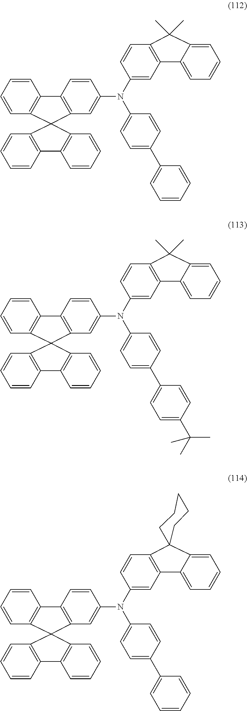


HOMO(eV)=((HEh*27.212)−0.9899)/1.1206
| Material | HOMO | ||
| HIM1/HTM1 | −5.25 eV | ||
| HIM 2 | −4.85 eV | ||
| NPB | −5.16 eV | ||
| HTM2 | −5.43 eV | ||
| HTM3 | −5.23 eV | ||
| HTM4 | −5.35 eV | ||
| HTM5 | −5.32 eV | ||
| HTM6 | −5.23 eV | ||
Part B: Production of OLEDs
| TABLE 1 |
| Structures of the materials used |
 |
| F4TCNQ |
 |
| HIM1 |
 |
| HIM2 |
 |
| H1 |
 |
| SEB1 |
 |
| SEB2 |
 |
| H2 |
 |
| TEG |
 |
| ETM |
 |
| LIQ |
 |
| NPB |
 |
| HTM1 |
 |
| HTM2 |
 |
| HTM3 |
 |
| HTM4 |
 |
| HTM5 |
 |
| HTM6 |
 |
| HAT-CN |
| TABLE 2 |
| Structure of the OLEDs |
| HIL1 | HTL | HIL2 | EBL | EML | ETL | EIL | |
| Ex. | Thickness/nm | Thickness/nm | Thickness/nm | Thickness/nm | Thickness/nm | Thickness/nm | Thickness/nm |
| V1 | HIM1:F4TCNQ(3%) | HIM1 | HTM1 | H1:SEB1(5%) | ETM(50%):LiQ(50%) | LiQ | |
| 20 nm | 175 nm | 20 nm | 20 nm | 30 nm | 1 nm | ||
| E1 | HIM1:F4TCNQ(3%) | HIM1 | HTM1:F4TCNQ(3%) | HTM1 | H1:SEB1(5%) | ETM(50%):LiQ(50%) | LiQ |
| 20 nm | 155 nm | 20 nm | 20 nm | 20 nm | 30 nm | 1 nm | |
| V2 | HIM1:F4TCNQ(3%) | HIM1 | HTM1 | H2:TEG(10%) | ETM(50%):LiQ(50%) | LiQ | |
| 20 nm | 210 nm | 20 nm | 40 nm | 30 nm | 1 nm | ||
| E2 | HIM1:F4TCNQ(3%) | HIM1 | HTM1:F4TCNQ(3%) | HTM1 | H2:TEG(10%) | ETM(50%):LiQ(50%) | LiQ |
| 20 nm | 190 nm | 20 nm | 20 nm | 40 nm | 30 nm | 1 nm | |
| V3 | HIM1:F4TCNQ(3%) | HIM1 | HTM2 | H1:SEB1(5%) | ETM(50%):LiQ(50%) | LiQ | |
| 20 nm | 175 nm | 20 nm | 20 nm | 30 nm | 1 nm | ||
| E3 | HIM1:F4TCNQ(3%) | HIM1 | HTM2:F4TCNQ(3%) | HTM2 | H1:SEB1(5%) | ETM(50%):LiQ(50%) | LiQ |
| 20 nm | 155 nm | 20 nm | 20 nm | 20 nm | 30 nm | 1 nm | |
| E4 | HIM1:F4TCNQ(3%) | HIM1 | HTM1:F4TCNQ(3%) | HTM2 | H1:SEB1(5%) | ETM(50%):LiQ(50%) | LiQ |
| 20 nm | 155 nm | 20 nm | 20 nm | 20 nm | 30 nm | 1 nm | |
| V4 | HIM1:F4TCNQ(3%) | HIM1 | HTM3 | H1:SEB1(5%) | ETM(50%):LiQ(50%) | LiQ | |
| 20 nm | 175 nm | 20 nm | 20 nm | 30 nm | 1 nm | ||
| E5 | HIM1:F4TCNQ(3%) | HIM1 | HTM3:F4TCNQ(3%) | HTM3 | H1:SEB1(5%) | ETM(50%):LiQ(50%) | LiQ |
| 20 nm | 155 nm | 20 nm | 20 nm | 20 nm | 30 nm | 1 nm | |
| E6 | HIM1:F4TCNQ(3%) | HIM1 | HTM1:F4TCNQ(3%) | HTM3 | H1:SEB1(5%) | ETM(50%):LiQ(50%) | LiQ |
| 20 nm | 155 nm | 20 nm | 20 nm | 20 nm | 30 nm | 1 nm | |
| V5 | HIM1:F4TCNQ(3%) | HIM1 | NPB | H1:SEB1(5%) | ETM | LiQ | |
| 20 nm | 175 nm | 20 nm | 20 nm | 30 nm | 3 nm | ||
| E7 | HIM1:F4TCNQ(3%) | HIM1 | NPB:F4TCNQ(3%) | NPB | H1:SEB1(5%) | ETM | LiQ |
| 20 nm | 155 nm | 20 nm | 20 nm | 20 nm | 30 nm | 3 nm | |
| V6 | HIM2:F4TCNQ(3%) | HIM2 | HTM1 | H1:SEB2(5%) | ETM(50%):LiQ(50%) | LiQ | |
| 10 nm | 140 nm | 30 nm | 20 nm | 30 nm | 1 nm | ||
| V7 | HIM2:F4TCNQ(3%) | HTM1 | H1:SEB2(5%) | ETM(50%):LiQ(50%) | LiQ | ||
| 150 nm | 30 nm | 20 nm | 30 nm | 1 nm | |||
| E8 | HIM2:F4TCNQ(3%) | HIM2 | HTM1:F4TCNQ(3%) | HTM1 | H1:SEB2(5%) | ETM(50%):LiQ(50%) | LiQ |
| 10 nm | 140 nm | 20 nm | 10 nm | 20 nm | 30 nm | 1 nm | |
| V8 | HIM1:F4TCNQ(3%) | HIM1 | HTM4 | H1:SEB1(5%) | ETM(50%):LiQ(50%) | LiQ | |
| 20 nm | 160 nm | 20 nm | 20 nm | 30 nm | 1 nm | ||
| E9 | HIM1:F4TCNQ(3%) | HIM1 | HTM5:F4TCNQ(3%) | HTM4 | H1:SEB1(5%) | ETM(50%):LiQ(50%) | LiQ |
| 20 nm | 140 nm | 20 nm | 20 nm | 20 nm | 30 nm | 1 nm | |
| V9 | HIM1:F4TCNQ(3%) | HIM1 | HTM5 | H1:SEB1(5%) | ETM(50%):LiQ(50%) | LiQ | |
| 20 nm | 175 nm | 20 nm | 20 nm | 30 nm | 1 nm | ||
| E10 | HIM1:F4TCNQ(3%) | HIM1 | HTM6:F4TCNQ(3%) | HTM5 | H1:SEB1(5%) | ETM(50%):LiQ(50%) | LiQ |
| 20 nm | 155 nm | 20 nm | 20 nm | 20 nm | 30 nm | 1 nm | |
| E11 | HIM1:F4TCNQ(3%) | HIM1 | HTM1:F4TCNQ(3%) | HTM5 | H1:SEB1(5%) | ETM(50%):LiQ(50%) | LiQ |
| 20 nm | 155 nm | 20 nm | 20 nm | 20 nm | 30 nm | 1 nm | |
| V10 | HIM1:F4TCNQ(3%) | HIM1 | HTM6 | H1:SEB1(5%) | ETM(50%):LiQ(50%) | LiQ | |
| 20 nm | 175 nm | 20 nm | 20 nm | 30 nm | 1 nm | ||
| E12 | HIM1:F4TCNQ(3%) | HIM1 | HTM6:F4TCNQ(3%) | HTM6 | H1:SEB1(5%) | ETM(50%):LiQ(50%) | LiQ |
| 20 nm | 155 nm | 20 nm | 20 nm | 20 nm | 30 nm | 1 nm | |
| E13 | HIM1:F4TCNQ(3%) | HIM1 | HTM1:F4TCNQ(3%) | HTM6 | H1:SEB1(5%) | ETM(50%):LiQ(50%) | LiQ |
| 20 nm | 155 nm | 20 nm | 20 nm | 20 nm | 30 nm | 1 nm | |
| V11 | HIM2:F4TCNQ(3%) | HIM2 | Hat-CN | HTM1 | H1:SEB2(5%) | ETM(50%):LiQ(50%) | LiQ |
| 10 nm | 140 nm | 10 nm | 20 nm | 20 nm | 30 nm | 1 nm | |
Claims (28)


Priority Applications (1)
| Application Number | Priority Date | Filing Date | Title |
|---|---|---|---|
| US15/870,165 US10270052B2 (en) | 2012-10-09 | 2018-01-12 | Electronic device |
Applications Claiming Priority (6)
| Application Number | Priority Date | Filing Date | Title |
|---|---|---|---|
| EP12006991 | 2012-10-09 | ||
| EP12006991 | 2012-10-09 | ||
| EP12006991.9 | 2012-10-09 | ||
| PCT/EP2013/002727 WO2014056565A1 (en) | 2012-10-09 | 2013-09-11 | Electronic device |
| US201514434277A | 2015-04-08 | 2015-04-08 | |
| US15/870,165 US10270052B2 (en) | 2012-10-09 | 2018-01-12 | Electronic device |
Related Parent Applications (2)
| Application Number | Title | Priority Date | Filing Date |
|---|---|---|---|
| PCT/EP2013/002727 Continuation WO2014056565A1 (en) | 2012-10-09 | 2013-09-11 | Electronic device |
| US14/434,277 Continuation US9917272B2 (en) | 2012-10-09 | 2013-09-11 | Electronic device |
Publications (2)
| Publication Number | Publication Date |
|---|---|
| US20180138439A1 US20180138439A1 (en) | 2018-05-17 |
| US10270052B2 true US10270052B2 (en) | 2019-04-23 |
Family
ID=47143484
Family Applications (2)
| Application Number | Title | Priority Date | Filing Date |
|---|---|---|---|
| US14/434,277 Active 2034-06-02 US9917272B2 (en) | 2012-10-09 | 2013-09-11 | Electronic device |
| US15/870,165 Active US10270052B2 (en) | 2012-10-09 | 2018-01-12 | Electronic device |
Family Applications Before (1)
| Application Number | Title | Priority Date | Filing Date |
|---|---|---|---|
| US14/434,277 Active 2034-06-02 US9917272B2 (en) | 2012-10-09 | 2013-09-11 | Electronic device |
Country Status (7)
| Country | Link |
|---|---|
| US (2) | US9917272B2 (en) |
| EP (1) | EP2907173B1 (en) |
| JP (2) | JP6449162B2 (en) |
| KR (4) | KR102007150B1 (en) |
| CN (2) | CN104718636B (en) |
| TW (1) | TWI637541B (en) |
| WO (1) | WO2014056565A1 (en) |
Cited By (1)
| Publication number | Priority date | Publication date | Assignee | Title |
|---|---|---|---|---|
| US11711973B2 (en) | 2019-08-02 | 2023-07-25 | Duk San Neolux Co., Ltd. | Organic electronic device |
Families Citing this family (39)
| Publication number | Priority date | Publication date | Assignee | Title |
|---|---|---|---|---|
| US9748492B2 (en) | 2012-11-02 | 2017-08-29 | Idemitsu Kosan Co., Ltd. | Organic electroluminescent device |
| JP6498688B2 (en) | 2014-02-28 | 2019-04-10 | メルク パテント ゲーエムベーハー | Materials for organic electroluminescent devices |
| KR102146367B1 (en) * | 2014-03-06 | 2020-08-21 | 삼성디스플레이 주식회사 | Organic light emitting diode device |
| CN104241540A (en) * | 2014-09-04 | 2014-12-24 | 京东方科技集团股份有限公司 | Organic electroluminescent display device, manufacturing method thereof and display unit |
| KR102448359B1 (en) | 2014-10-06 | 2022-09-29 | 삼성디스플레이 주식회사 | Organic electroluminescent device |
| KR102401598B1 (en) | 2014-11-07 | 2022-05-25 | 삼성디스플레이 주식회사 | Organic electroluminescence device |
| KR101796288B1 (en) * | 2014-12-02 | 2017-11-13 | 삼성디스플레이 주식회사 | Organic electroluminescence device |
| EP3032605B1 (en) * | 2014-12-08 | 2019-08-21 | LG Display Co., Ltd. | Organic light emitting display device |
| CN107207550B (en) | 2015-02-03 | 2020-06-05 | 默克专利有限公司 | Metal complexes |
| KR102624166B1 (en) * | 2015-06-15 | 2024-01-12 | 삼성디스플레이 주식회사 | Organic electroluminescence device |
| TWI648279B (en) * | 2015-11-17 | 2019-01-21 | 南韓商Lg化學股份有限公司 | Compound having a spiro structure and organic light-emitting device comprising the same |
| DE102016104764A1 (en) * | 2016-03-15 | 2017-09-21 | Osram Oled Gmbh | Organic light-emitting diode and automotive taillight |
| TWI764942B (en) * | 2016-10-10 | 2022-05-21 | 德商麥克專利有限公司 | Electronic device |
| CN108164532A (en) * | 2016-12-07 | 2018-06-15 | 季昀 | Organic compound with class tetrahedron configuration |
| EP3590141A1 (en) * | 2017-03-01 | 2020-01-08 | Merck Patent GmbH | Organic electroluminescent device |
| US11767299B2 (en) | 2017-06-23 | 2023-09-26 | Merck Patent Gmbh | Materials for organic electroluminescent devices |
| CN109216565B (en) * | 2017-06-30 | 2021-05-18 | 昆山国显光电有限公司 | Organic electroluminescent device and preparation method thereof |
| TWI776926B (en) | 2017-07-25 | 2022-09-11 | 德商麥克專利有限公司 | Metal complexes |
| TWI791701B (en) | 2017-12-13 | 2023-02-11 | 德商麥克專利有限公司 | Metal complexes |
| CN111699192B (en) | 2018-02-13 | 2024-03-08 | Udc爱尔兰有限公司 | Metal complex |
| US20210020843A1 (en) | 2018-03-16 | 2021-01-21 | Merck Patent Gmbh | Materials for organic electroluminescent devices |
| KR20210024995A (en) * | 2018-06-25 | 2021-03-08 | 호도가야 가가쿠 고교 가부시키가이샤 | Compound with triarylamine structure and organic electroluminescent device |
| CN109004092A (en) * | 2018-06-29 | 2018-12-14 | 云谷(固安)科技有限公司 | Organic electroluminescence device and Organnic electroluminescent device |
| US20210257550A1 (en) | 2018-07-03 | 2021-08-19 | Lg Chem, Ltd. | Polycyclic compound and organic light emitting diode comprising same |
| KR20200094262A (en) | 2019-01-29 | 2020-08-07 | 삼성디스플레이 주식회사 | Organic electroluminescence device and polycyclic compound for organic electroluminescence device |
| TW202043247A (en) | 2019-02-11 | 2020-12-01 | 德商麥克專利有限公司 | Metal complexes |
| WO2021025371A1 (en) * | 2019-08-02 | 2021-02-11 | 덕산네오룩스 주식회사 | Organic electronic device |
| CN114207859A (en) * | 2019-08-02 | 2022-03-18 | 德山新勒克斯有限公司 | Organic electronic device |
| CN112552301A (en) * | 2019-09-26 | 2021-03-26 | 广州华睿光电材料有限公司 | Indoloquinone organic compound and application thereof |
| CN110635058B (en) * | 2019-09-26 | 2022-04-08 | 昆山国显光电有限公司 | Organic light-emitting device and display panel |
| JP2023504723A (en) | 2019-12-04 | 2023-02-06 | メルク パテント ゲゼルシャフト ミット ベシュレンクテル ハフツング | metal complex |
| KR20210084744A (en) * | 2019-12-27 | 2021-07-08 | 삼성디스플레이 주식회사 | Organic light emitting device and apparatus including the same |
| JP7295824B2 (en) * | 2020-03-31 | 2023-06-21 | 双葉電子工業株式会社 | Organic EL device |
| EP4222155A1 (en) | 2020-09-29 | 2023-08-09 | Merck Patent GmbH | Mononuclear tripodal hexadentate iridium complexes for use in oleds |
| EP4079742A1 (en) | 2021-04-14 | 2022-10-26 | Merck Patent GmbH | Metal complexes |
| KR20230077804A (en) | 2021-11-25 | 2023-06-02 | 삼성디스플레이 주식회사 | Light emitting display device |
| KR20230096204A (en) | 2021-12-22 | 2023-06-30 | 삼성디스플레이 주식회사 | Pixel and display device including the same |
| KR20230161590A (en) | 2022-05-18 | 2023-11-28 | 삼성디스플레이 주식회사 | Light emitting display device |
| KR20240018019A (en) | 2022-08-01 | 2024-02-13 | 삼성디스플레이 주식회사 | Display device and method of driving the same |
Citations (40)
| Publication number | Priority date | Publication date | Assignee | Title |
|---|---|---|---|---|
| US6423429B2 (en) | 1998-03-02 | 2002-07-23 | Junji Kido | Organic electroluminescent devices |
| US20030170491A1 (en) | 2002-02-15 | 2003-09-11 | Eastman Kodak Company | Providing an organic electroluminescent device having stacked electroluminescent units |
| WO2004091262A1 (en) | 2003-04-02 | 2004-10-21 | Fujitsu Limited | Organic electroluminescence element and organic electroluminescence display |
| CN1589073A (en) | 2004-06-28 | 2005-03-02 | 友达光电股份有限公司 | Organic luminous display element and its producing method |
| US20050255334A1 (en) | 2004-05-11 | 2005-11-17 | Minsoo Kang | Organic electronic device |
| US20060022585A1 (en) | 2004-08-02 | 2006-02-02 | Xerox Corporation | OLEDs having improved luminance stability |
| WO2006122630A1 (en) | 2005-05-20 | 2006-11-23 | Merck Patent Gmbh | Compounds for organic electronic devices |
| US20070098891A1 (en) | 2005-10-31 | 2007-05-03 | Eastman Kodak Company | Vapor deposition apparatus and method |
| US20070126348A1 (en) | 2005-12-01 | 2007-06-07 | Au Optronics Corp. | Organic electroluminescent device |
| US20070141396A1 (en) | 2005-12-20 | 2007-06-21 | Min-Seung Chun | Organic luminescence display device and method of manufacturing the same |
| US20070231596A1 (en) | 2006-03-30 | 2007-10-04 | Eastman Kodak Company | OLED device with improved efficiency and lifetime |
| JP2008019238A (en) | 2005-12-20 | 2008-01-31 | Canon Inc | 4-aminofluorene compound and organic light emitting device |
| JP2008177455A (en) | 2007-01-22 | 2008-07-31 | Toray Ind Inc | Light-emitting element |
| US20080193793A1 (en) | 2004-12-23 | 2008-08-14 | Technische Universitaet Braunschweig | Material For Doped And Undoped Hole And Electron Transport Layer |
| KR20080090350A (en) | 2007-04-03 | 2008-10-08 | 칭화 유니버시티 | Organic electroluminescent device |
| US20080297036A1 (en) | 2007-05-31 | 2008-12-04 | Tae-Yong Noh | White organic light emitting device |
| JP2009071189A (en) | 2007-09-14 | 2009-04-02 | Fujifilm Corp | Organic electroluminescent device |
| US20090315022A1 (en) | 2007-11-30 | 2009-12-24 | Idemitsu Kosan Co., Ltd. | Azaindenofluorenedione derivative, material for organic electroluminescence device and organic electroluminescence device |
| US20100045175A1 (en) | 2008-08-19 | 2010-02-25 | Plexotronics, Inc. | Organic light emitting diode lighting devices |
| JP2010123716A (en) | 2008-11-19 | 2010-06-03 | Fujifilm Corp | Organic electroluminescent element |
| US20100288362A1 (en) | 2009-05-13 | 2010-11-18 | Hatwar Tukaram K | Internal connector for organic electronic devices |
| US20110108818A1 (en) | 2008-12-17 | 2011-05-12 | Merck Patent Gmbh | Organic electroluminescence device |
| US20110203649A1 (en) | 2010-02-19 | 2011-08-25 | Basf Se | Use of indanthrene compounds in organic photovoltaics |
| US20110215308A1 (en) | 2010-03-08 | 2011-09-08 | Samsung Mobile Display Co., Ltd. | Organic light-emitting device and method of manufacturing the same |
| US20110233604A1 (en) | 2010-03-24 | 2011-09-29 | Takeshi Ikeda | Organic electroluminescence device |
| US20110256422A1 (en) | 2008-10-31 | 2011-10-20 | Basf Se | Merocyanines for producing photoactive layers for organic solar cells and organic photodetectors |
| KR20110125861A (en) | 2010-05-14 | 2011-11-22 | 삼성모바일디스플레이주식회사 | Organic light emitting device |
| CN102270655A (en) | 2010-06-03 | 2011-12-07 | 佳能株式会社 | Display device |
| US20120012820A1 (en) | 2010-07-16 | 2012-01-19 | Idemitsu Kosan Co., Ltd. | Organic electroluminescence device and method for producing organic electroluminescence device |
| WO2012034627A1 (en) | 2010-09-15 | 2012-03-22 | Merck Patent Gmbh | Materials for organic electroluminescent devices |
| US20120074392A1 (en) | 2010-09-24 | 2012-03-29 | Novaled Ag | Tandem White OLED |
| US20120076836A1 (en) | 2009-03-31 | 2012-03-29 | The University Of Tokyo | Polyion complex of double-stranded ribonucleic acid |
| WO2012073269A1 (en) | 2010-11-29 | 2012-06-07 | パナソニック株式会社 | Organic electroluminescence panel, method of manufacturing organic electroluminescence panel, organic light emitting apparatus using organic electroluminescence panel, and organic display apparatus using organic electroluminescence panel |
| WO2012076836A1 (en) | 2010-12-06 | 2012-06-14 | Cambridge Display Technology Limited | Hole injection layers |
| JP2012182443A (en) | 2011-02-11 | 2012-09-20 | Semiconductor Energy Lab Co Ltd | Light-emitting element and light-emitting device |
| WO2013083216A1 (en) | 2011-11-17 | 2013-06-13 | Merck Patent Gmbh | Spiro dihydroacridine derivatives and the use thereof as materials for organic electroluminescence devices |
| WO2013135352A1 (en) | 2012-03-15 | 2013-09-19 | Merck Patent Gmbh | Electronic devices |
| US20130284977A1 (en) | 2010-12-15 | 2013-10-31 | Merck Patent Gmbh | Metal complexes |
| US20160099421A1 (en) | 2014-10-01 | 2016-04-07 | Samsung Display Co., Ltd. | Compound and organic light-emitting device including the same |
| US20160343776A1 (en) | 2015-05-23 | 2016-11-24 | Lg Display Co., Ltd. | Organic Light Emitting Device |
Family Cites Families (3)
| Publication number | Priority date | Publication date | Assignee | Title |
|---|---|---|---|---|
| JP4300176B2 (en) * | 2003-11-13 | 2009-07-22 | ローム株式会社 | Organic electroluminescent device |
| EP2415752B1 (en) * | 2009-03-19 | 2016-03-09 | Idemitsu Kosan Co., Ltd. | Aromatic amine derivative and organic electroluminescent element using same |
| KR101097315B1 (en) * | 2009-10-12 | 2011-12-23 | 삼성모바일디스플레이주식회사 | Organic light emitting device |
-
2013
- 2013-09-11 KR KR1020187008238A patent/KR102007150B1/en active IP Right Grant
- 2013-09-11 JP JP2015536003A patent/JP6449162B2/en active Active
- 2013-09-11 KR KR1020197022140A patent/KR102071843B1/en active IP Right Grant
- 2013-09-11 US US14/434,277 patent/US9917272B2/en active Active
- 2013-09-11 EP EP13763188.3A patent/EP2907173B1/en active Active
- 2013-09-11 WO PCT/EP2013/002727 patent/WO2014056565A1/en active Application Filing
- 2013-09-11 CN CN201380052539.5A patent/CN104718636B/en active Active
- 2013-09-11 KR KR1020187008239A patent/KR102153871B1/en active IP Right Grant
- 2013-09-11 CN CN201811030435.5A patent/CN109346615B/en active Active
- 2013-09-11 KR KR1020157012027A patent/KR102023232B1/en active IP Right Grant
- 2013-10-08 TW TW102136390A patent/TWI637541B/en active
-
2018
- 2018-01-12 US US15/870,165 patent/US10270052B2/en active Active
- 2018-12-05 JP JP2018228038A patent/JP6821637B2/en active Active
Patent Citations (59)
| Publication number | Priority date | Publication date | Assignee | Title |
|---|---|---|---|---|
| US6423429B2 (en) | 1998-03-02 | 2002-07-23 | Junji Kido | Organic electroluminescent devices |
| US20030170491A1 (en) | 2002-02-15 | 2003-09-11 | Eastman Kodak Company | Providing an organic electroluminescent device having stacked electroluminescent units |
| WO2004091262A1 (en) | 2003-04-02 | 2004-10-21 | Fujitsu Limited | Organic electroluminescence element and organic electroluminescence display |
| US7449832B2 (en) | 2003-04-02 | 2008-11-11 | Fuji Photo Film Co., Ltd. | Organic electroluminescence device and organic electroluminescence display |
| US20050255334A1 (en) | 2004-05-11 | 2005-11-17 | Minsoo Kang | Organic electronic device |
| CN1589073A (en) | 2004-06-28 | 2005-03-02 | 友达光电股份有限公司 | Organic luminous display element and its producing method |
| US20060022585A1 (en) | 2004-08-02 | 2006-02-02 | Xerox Corporation | OLEDs having improved luminance stability |
| US20080193793A1 (en) | 2004-12-23 | 2008-08-14 | Technische Universitaet Braunschweig | Material For Doped And Undoped Hole And Electron Transport Layer |
| WO2006122630A1 (en) | 2005-05-20 | 2006-11-23 | Merck Patent Gmbh | Compounds for organic electronic devices |
| US20150031896A1 (en) | 2005-05-20 | 2015-01-29 | Merck Patent Gmbh | Compounds for organic electronic devices |
| US8852756B2 (en) | 2005-05-20 | 2014-10-07 | Merck Patent Gmbh | Materials for organic electroluminescent devices |
| CN101228250A (en) | 2005-05-20 | 2008-07-23 | 默克专利有限公司 | Compounds for organic electronic devices |
| US20070098891A1 (en) | 2005-10-31 | 2007-05-03 | Eastman Kodak Company | Vapor deposition apparatus and method |
| US20070126348A1 (en) | 2005-12-01 | 2007-06-07 | Au Optronics Corp. | Organic electroluminescent device |
| TWI299636B (en) | 2005-12-01 | 2008-08-01 | Au Optronics Corp | Organic light emitting diode |
| EP1801882A2 (en) | 2005-12-20 | 2007-06-27 | Samsung SDI Co., Ltd. | Organic luminescence display device and method of manufacturing the same |
| JP2008019238A (en) | 2005-12-20 | 2008-01-31 | Canon Inc | 4-aminofluorene compound and organic light emitting device |
| US8691398B2 (en) | 2005-12-20 | 2014-04-08 | Canon Kabushiki Kaisha | 4-aminofluorene compound and organic light emitting device |
| US20070141396A1 (en) | 2005-12-20 | 2007-06-21 | Min-Seung Chun | Organic luminescence display device and method of manufacturing the same |
| US20070231596A1 (en) | 2006-03-30 | 2007-10-04 | Eastman Kodak Company | OLED device with improved efficiency and lifetime |
| JP2008177455A (en) | 2007-01-22 | 2008-07-31 | Toray Ind Inc | Light-emitting element |
| KR20080090350A (en) | 2007-04-03 | 2008-10-08 | 칭화 유니버시티 | Organic electroluminescent device |
| US20090001878A1 (en) | 2007-04-03 | 2009-01-01 | Tsinghua University | Organic electroluminescent device |
| US20080297036A1 (en) | 2007-05-31 | 2008-12-04 | Tae-Yong Noh | White organic light emitting device |
| JP2009071189A (en) | 2007-09-14 | 2009-04-02 | Fujifilm Corp | Organic electroluminescent device |
| US20090315022A1 (en) | 2007-11-30 | 2009-12-24 | Idemitsu Kosan Co., Ltd. | Azaindenofluorenedione derivative, material for organic electroluminescence device and organic electroluminescence device |
| US20100045175A1 (en) | 2008-08-19 | 2010-02-25 | Plexotronics, Inc. | Organic light emitting diode lighting devices |
| US20110256422A1 (en) | 2008-10-31 | 2011-10-20 | Basf Se | Merocyanines for producing photoactive layers for organic solar cells and organic photodetectors |
| JP2010123716A (en) | 2008-11-19 | 2010-06-03 | Fujifilm Corp | Organic electroluminescent element |
| US20110108818A1 (en) | 2008-12-17 | 2011-05-12 | Merck Patent Gmbh | Organic electroluminescence device |
| US20120076836A1 (en) | 2009-03-31 | 2012-03-29 | The University Of Tokyo | Polyion complex of double-stranded ribonucleic acid |
| US20100288362A1 (en) | 2009-05-13 | 2010-11-18 | Hatwar Tukaram K | Internal connector for organic electronic devices |
| US20110203649A1 (en) | 2010-02-19 | 2011-08-25 | Basf Se | Use of indanthrene compounds in organic photovoltaics |
| US20110215308A1 (en) | 2010-03-08 | 2011-09-08 | Samsung Mobile Display Co., Ltd. | Organic light-emitting device and method of manufacturing the same |
| KR20110101418A (en) | 2010-03-08 | 2011-09-16 | 삼성모바일디스플레이주식회사 | Organic light emitting diode and method for preparing the same |
| EP2365555A2 (en) | 2010-03-08 | 2011-09-14 | Samsung Mobile Display Co., Ltd. | Organic light-emitting device and method of manufacturing the same |
| CN102201432A (en) | 2010-03-08 | 2011-09-28 | 三星移动显示器株式会社 | Organic light-emitting device and method of manufacturing the same |
| US9472767B2 (en) | 2010-03-08 | 2016-10-18 | Samsung Display Co., Ltd. | Organic light-emitting device and method of manufacturing the same |
| JP2011187959A (en) | 2010-03-08 | 2011-09-22 | Samsung Mobile Display Co Ltd | Organic light-emitting device, and method of manufacturing the same |
| US20110233604A1 (en) | 2010-03-24 | 2011-09-29 | Takeshi Ikeda | Organic electroluminescence device |
| KR20110125861A (en) | 2010-05-14 | 2011-11-22 | 삼성모바일디스플레이주식회사 | Organic light emitting device |
| US9136495B2 (en) | 2010-05-14 | 2015-09-15 | Samsung Display Co., Ltd. | Organic light-emitting device |
| CN102270655A (en) | 2010-06-03 | 2011-12-07 | 佳能株式会社 | Display device |
| US20110297977A1 (en) | 2010-06-03 | 2011-12-08 | Canon Kabushiki Kaisha | Display device |
| US20120012820A1 (en) | 2010-07-16 | 2012-01-19 | Idemitsu Kosan Co., Ltd. | Organic electroluminescence device and method for producing organic electroluminescence device |
| US20160190447A1 (en) | 2010-09-15 | 2016-06-30 | Merck Patent Gmbh | Materials for organic electroluminescent devices |
| WO2012034627A1 (en) | 2010-09-15 | 2012-03-22 | Merck Patent Gmbh | Materials for organic electroluminescent devices |
| US20120074392A1 (en) | 2010-09-24 | 2012-03-29 | Novaled Ag | Tandem White OLED |
| US8957412B2 (en) | 2010-11-29 | 2015-02-17 | Panasonic Corporation | Organic electroluminescence panel, method of manufacturing organic electroluminescence panel, organic light emitting apparatus using organic electroluminescence panel, and organic display apparatus using organic electroluminescence panel |
| WO2012073269A1 (en) | 2010-11-29 | 2012-06-07 | パナソニック株式会社 | Organic electroluminescence panel, method of manufacturing organic electroluminescence panel, organic light emitting apparatus using organic electroluminescence panel, and organic display apparatus using organic electroluminescence panel |
| WO2012076836A1 (en) | 2010-12-06 | 2012-06-14 | Cambridge Display Technology Limited | Hole injection layers |
| US20130284977A1 (en) | 2010-12-15 | 2013-10-31 | Merck Patent Gmbh | Metal complexes |
| US9088002B2 (en) | 2011-02-11 | 2015-07-21 | Semiconductor Energy Laboratory Co., Ltd. | Light-emitting device and manufacturing method thereof |
| JP2012182443A (en) | 2011-02-11 | 2012-09-20 | Semiconductor Energy Lab Co Ltd | Light-emitting element and light-emitting device |
| US20140316134A1 (en) | 2011-11-17 | 2014-10-23 | Merck Patent Gmbh | Spiro dihydroacridine derivatives and the use thereof as materials for organic electroluminescence devices |
| WO2013083216A1 (en) | 2011-11-17 | 2013-06-13 | Merck Patent Gmbh | Spiro dihydroacridine derivatives and the use thereof as materials for organic electroluminescence devices |
| WO2013135352A1 (en) | 2012-03-15 | 2013-09-19 | Merck Patent Gmbh | Electronic devices |
| US20160099421A1 (en) | 2014-10-01 | 2016-04-07 | Samsung Display Co., Ltd. | Compound and organic light-emitting device including the same |
| US20160343776A1 (en) | 2015-05-23 | 2016-11-24 | Lg Display Co., Ltd. | Organic Light Emitting Device |
Non-Patent Citations (5)
| Title |
|---|
| Chinese Office Action for application No. 201380052539.5, dated May 4, 2016. |
| English Translation of Korean Office Action for Korean Application No. 10-2015-7012027, dated Jul. 26, 2017. |
| International Search Report for PCT/EP2013/002727 dated Oct. 16, 2013. |
| Japanese Office Action for Japanese Application No. 2015-536003, dated Jul. 4, 2017. |
| Zhou et al., "Very-low-operating-voltage organic light-emitting diodes using a p-doped amorphous hole injection layer", Applied Physics Letters, 78(4), pp. 410-412, 2001. |
Cited By (1)
| Publication number | Priority date | Publication date | Assignee | Title |
|---|---|---|---|---|
| US11711973B2 (en) | 2019-08-02 | 2023-07-25 | Duk San Neolux Co., Ltd. | Organic electronic device |
Also Published As
| Publication number | Publication date |
|---|---|
| KR20180034693A (en) | 2018-04-04 |
| KR102007150B1 (en) | 2019-08-05 |
| JP2019062216A (en) | 2019-04-18 |
| CN104718636B (en) | 2018-09-25 |
| KR20150067331A (en) | 2015-06-17 |
| KR20190090893A (en) | 2019-08-02 |
| US9917272B2 (en) | 2018-03-13 |
| TW201417369A (en) | 2014-05-01 |
| KR102153871B1 (en) | 2020-09-09 |
| CN109346615B (en) | 2021-06-04 |
| KR20180034692A (en) | 2018-04-04 |
| JP6821637B2 (en) | 2021-01-27 |
| JP6449162B2 (en) | 2019-01-09 |
| TWI637541B (en) | 2018-10-01 |
| EP2907173A1 (en) | 2015-08-19 |
| CN104718636A (en) | 2015-06-17 |
| JP2016500917A (en) | 2016-01-14 |
| KR102023232B1 (en) | 2019-09-19 |
| US20150270506A1 (en) | 2015-09-24 |
| US20180138439A1 (en) | 2018-05-17 |
| KR102071843B1 (en) | 2020-01-31 |
| CN109346615A (en) | 2019-02-15 |
| EP2907173B1 (en) | 2018-03-21 |
| WO2014056565A1 (en) | 2014-04-17 |
Similar Documents
| Publication | Publication Date | Title |
|---|---|---|
| US10270052B2 (en) | Electronic device | |
| US9871201B2 (en) | Electronic devices | |
| US10249828B2 (en) | Organic electroluminescent device | |
| US10454040B2 (en) | Materials for electronic devices | |
| US10727413B2 (en) | Materials for electronic devices | |
| US10193094B2 (en) | Organic light-emitting device having delayed fluorescence | |
| US20220181552A1 (en) | Materials for organic electroluminescent devices | |
| US10407394B2 (en) | Triarylamine-substituted benzo[H]quinoline-derivatives as materials for electronic devices | |
| US10396297B2 (en) | Materials for electronic devices | |
| US11778907B2 (en) | Composition for organic electronic devices | |
| US11393987B2 (en) | Organic electroluminescent device | |
| US20220048836A1 (en) | Materials for organic electroluminescent devices | |
| US20220231226A1 (en) | Electronic device | |
| US11631816B2 (en) | Electronic device | |
| US20230016716A1 (en) | Materials for organic electroluminescent devices | |
| US20220199908A1 (en) | Electronic device | |
| US20150340636A1 (en) | Electronic Device | |
| KR20210096630A (en) | electronic device | |
| US9246118B2 (en) | Organic electroluminescent device | |
| US20230108986A1 (en) | Electronic device |
Legal Events
| Date | Code | Title | Description |
|---|---|---|---|
| FEPP | Fee payment procedure |
Free format text: ENTITY STATUS SET TO UNDISCOUNTED (ORIGINAL EVENT CODE: BIG.); ENTITY STATUS OF PATENT OWNER: LARGE ENTITY |
|
| AS | Assignment |
Owner name: MERCK PATENT GMBH, GERMANY Free format text: ASSIGNMENT OF ASSIGNORS INTEREST;ASSIGNORS:VOGES, FRANK;KROEBER, JONAS VALENTIN;PFLUMM, CHRISTOF;AND OTHERS;SIGNING DATES FROM 20150202 TO 20150302;REEL/FRAME:045545/0818 |
|
| STPP | Information on status: patent application and granting procedure in general |
Free format text: PUBLICATIONS -- ISSUE FEE PAYMENT VERIFIED |
|
| STCF | Information on status: patent grant |
Free format text: PATENTED CASE |
|
| MAFP | Maintenance fee payment |
Free format text: PAYMENT OF MAINTENANCE FEE, 4TH YEAR, LARGE ENTITY (ORIGINAL EVENT CODE: M1551); ENTITY STATUS OF PATENT OWNER: LARGE ENTITY Year of fee payment: 4 |