US10212818B2 - Methods and apparatus for a substrate core layer - Google Patents
Methods and apparatus for a substrate core layer Download PDFInfo
- Publication number
- US10212818B2 US10212818B2 US16/001,416 US201816001416A US10212818B2 US 10212818 B2 US10212818 B2 US 10212818B2 US 201816001416 A US201816001416 A US 201816001416A US 10212818 B2 US10212818 B2 US 10212818B2
- Authority
- US
- United States
- Prior art keywords
- die
- conductive layer
- dielectric layer
- layer
- molding compound
- Prior art date
- Legal status (The legal status is an assumption and is not a legal conclusion. Google has not performed a legal analysis and makes no representation as to the accuracy of the status listed.)
- Active
Links
- 238000000034 method Methods 0.000 title claims abstract description 63
- 239000000758 substrate Substances 0.000 title claims abstract description 60
- 239000012792 core layer Substances 0.000 title claims abstract description 42
- 239000010410 layer Substances 0.000 claims abstract description 261
- 238000000465 moulding Methods 0.000 claims abstract description 67
- 229910052751 metal Inorganic materials 0.000 claims abstract description 48
- 239000002184 metal Substances 0.000 claims abstract description 48
- 150000001875 compounds Chemical class 0.000 claims abstract description 42
- 229920002120 photoresistant polymer Polymers 0.000 claims description 17
- 239000000463 material Substances 0.000 claims description 15
- RYGMFSIKBFXOCR-UHFFFAOYSA-N Copper Chemical compound [Cu] RYGMFSIKBFXOCR-UHFFFAOYSA-N 0.000 claims description 11
- 239000010949 copper Substances 0.000 claims description 11
- 229920005989 resin Polymers 0.000 claims description 11
- 239000011347 resin Substances 0.000 claims description 11
- 229910052802 copper Inorganic materials 0.000 claims description 9
- 238000005530 etching Methods 0.000 claims description 9
- 238000007747 plating Methods 0.000 claims description 9
- 239000004642 Polyimide Substances 0.000 claims description 5
- 229920000106 Liquid crystal polymer Polymers 0.000 claims description 4
- 239000004977 Liquid-crystal polymers (LCPs) Substances 0.000 claims description 4
- PXHVJJICTQNCMI-UHFFFAOYSA-N Nickel Chemical compound [Ni] PXHVJJICTQNCMI-UHFFFAOYSA-N 0.000 claims description 4
- ATJFFYVFTNAWJD-UHFFFAOYSA-N Tin Chemical compound [Sn] ATJFFYVFTNAWJD-UHFFFAOYSA-N 0.000 claims description 4
- JYEUMXHLPRZUAT-UHFFFAOYSA-N 1,2,3-triazine Chemical compound C1=CN=NN=C1 JYEUMXHLPRZUAT-UHFFFAOYSA-N 0.000 claims description 3
- XQUPVDVFXZDTLT-UHFFFAOYSA-N 1-[4-[[4-(2,5-dioxopyrrol-1-yl)phenyl]methyl]phenyl]pyrrole-2,5-dione Chemical compound O=C1C=CC(=O)N1C(C=C1)=CC=C1CC1=CC=C(N2C(C=CC2=O)=O)C=C1 XQUPVDVFXZDTLT-UHFFFAOYSA-N 0.000 claims description 3
- 241000531908 Aramides Species 0.000 claims description 3
- 229920003235 aromatic polyamide Polymers 0.000 claims description 3
- 238000005553 drilling Methods 0.000 claims description 3
- 238000007772 electroless plating Methods 0.000 claims description 3
- 229920003192 poly(bis maleimide) Polymers 0.000 claims description 3
- VYZAMTAEIAYCRO-UHFFFAOYSA-N Chromium Chemical compound [Cr] VYZAMTAEIAYCRO-UHFFFAOYSA-N 0.000 claims description 2
- 229910000599 Cr alloy Inorganic materials 0.000 claims description 2
- 229910000881 Cu alloy Inorganic materials 0.000 claims description 2
- 229910000978 Pb alloy Inorganic materials 0.000 claims description 2
- 229910001128 Sn alloy Inorganic materials 0.000 claims description 2
- RTAQQCXQSZGOHL-UHFFFAOYSA-N Titanium Chemical compound [Ti] RTAQQCXQSZGOHL-UHFFFAOYSA-N 0.000 claims description 2
- 229910052804 chromium Inorganic materials 0.000 claims description 2
- 239000011651 chromium Substances 0.000 claims description 2
- 239000000788 chromium alloy Substances 0.000 claims description 2
- 229910052759 nickel Inorganic materials 0.000 claims description 2
- 238000000059 patterning Methods 0.000 claims description 2
- 229910052718 tin Inorganic materials 0.000 claims description 2
- 239000011135 tin Substances 0.000 claims description 2
- 239000010936 titanium Substances 0.000 claims description 2
- 229910052719 titanium Inorganic materials 0.000 claims description 2
- 239000004020 conductor Substances 0.000 claims 5
- KSAVQLQVUXSOCR-UHFFFAOYSA-M sodium lauroyl sarcosinate Chemical compound [Na+].CCCCCCCCCCCC(=O)N(C)CC([O-])=O KSAVQLQVUXSOCR-UHFFFAOYSA-M 0.000 description 25
- 238000004519 manufacturing process Methods 0.000 description 12
- 238000004806 packaging method and process Methods 0.000 description 11
- 230000008569 process Effects 0.000 description 11
- 238000005516 engineering process Methods 0.000 description 8
- 229910000679 solder Inorganic materials 0.000 description 8
- 239000000203 mixture Substances 0.000 description 5
- 239000004065 semiconductor Substances 0.000 description 5
- XUIMIQQOPSSXEZ-UHFFFAOYSA-N Silicon Chemical compound [Si] XUIMIQQOPSSXEZ-UHFFFAOYSA-N 0.000 description 3
- 230000008901 benefit Effects 0.000 description 3
- 230000010354 integration Effects 0.000 description 3
- 238000012536 packaging technology Methods 0.000 description 3
- 229910052710 silicon Inorganic materials 0.000 description 3
- 239000010703 silicon Substances 0.000 description 3
- 239000003822 epoxy resin Substances 0.000 description 2
- 239000011152 fibreglass Substances 0.000 description 2
- 230000006872 improvement Effects 0.000 description 2
- 229920000647 polyepoxide Polymers 0.000 description 2
- 238000005476 soldering Methods 0.000 description 2
- 230000004075 alteration Effects 0.000 description 1
- 239000003990 capacitor Substances 0.000 description 1
- 239000000919 ceramic Substances 0.000 description 1
- 230000002860 competitive effect Effects 0.000 description 1
- MPTQRFCYZCXJFQ-UHFFFAOYSA-L copper(II) chloride dihydrate Chemical compound O.O.[Cl-].[Cl-].[Cu+2] MPTQRFCYZCXJFQ-UHFFFAOYSA-L 0.000 description 1
- 238000000608 laser ablation Methods 0.000 description 1
- 239000004033 plastic Substances 0.000 description 1
- 150000003071 polychlorinated biphenyls Chemical class 0.000 description 1
- 230000009467 reduction Effects 0.000 description 1
- 238000004544 sputter deposition Methods 0.000 description 1
- 238000006467 substitution reaction Methods 0.000 description 1
Images


Classifications
-
- H—ELECTRICITY
- H05—ELECTRIC TECHNIQUES NOT OTHERWISE PROVIDED FOR
- H05K—PRINTED CIRCUITS; CASINGS OR CONSTRUCTIONAL DETAILS OF ELECTRIC APPARATUS; MANUFACTURE OF ASSEMBLAGES OF ELECTRICAL COMPONENTS
- H05K1/00—Printed circuits
- H05K1/18—Printed circuits structurally associated with non-printed electric components
- H05K1/182—Printed circuits structurally associated with non-printed electric components associated with components mounted in the printed circuit board, e.g. insert mounted components [IMC]
- H05K1/185—Components encapsulated in the insulating substrate of the printed circuit or incorporated in internal layers of a multilayer circuit
- H05K1/186—Components encapsulated in the insulating substrate of the printed circuit or incorporated in internal layers of a multilayer circuit manufactured by mounting on or connecting to patterned circuits before or during embedding
-
- H—ELECTRICITY
- H01—ELECTRIC ELEMENTS
- H01L—SEMICONDUCTOR DEVICES NOT COVERED BY CLASS H10
- H01L23/00—Details of semiconductor or other solid state devices
- H01L23/48—Arrangements for conducting electric current to or from the solid state body in operation, e.g. leads, terminal arrangements ; Selection of materials therefor
- H01L23/488—Arrangements for conducting electric current to or from the solid state body in operation, e.g. leads, terminal arrangements ; Selection of materials therefor consisting of soldered or bonded constructions
- H01L23/498—Leads, i.e. metallisations or lead-frames on insulating substrates, e.g. chip carriers
- H01L23/49827—Via connections through the substrates, e.g. pins going through the substrate, coaxial cables
-
- H—ELECTRICITY
- H01—ELECTRIC ELEMENTS
- H01L—SEMICONDUCTOR DEVICES NOT COVERED BY CLASS H10
- H01L23/00—Details of semiconductor or other solid state devices
- H01L23/52—Arrangements for conducting electric current within the device in operation from one component to another, i.e. interconnections, e.g. wires, lead frames
- H01L23/538—Arrangements for conducting electric current within the device in operation from one component to another, i.e. interconnections, e.g. wires, lead frames the interconnection structure between a plurality of semiconductor chips being formed on, or in, insulating substrates
- H01L23/5389—Arrangements for conducting electric current within the device in operation from one component to another, i.e. interconnections, e.g. wires, lead frames the interconnection structure between a plurality of semiconductor chips being formed on, or in, insulating substrates the chips being integrally enclosed by the interconnect and support structures
-
- H—ELECTRICITY
- H01—ELECTRIC ELEMENTS
- H01L—SEMICONDUCTOR DEVICES NOT COVERED BY CLASS H10
- H01L24/00—Arrangements for connecting or disconnecting semiconductor or solid-state bodies; Methods or apparatus related thereto
- H01L24/01—Means for bonding being attached to, or being formed on, the surface to be connected, e.g. chip-to-package, die-attach, "first-level" interconnects; Manufacturing methods related thereto
- H01L24/18—High density interconnect [HDI] connectors; Manufacturing methods related thereto
- H01L24/19—Manufacturing methods of high density interconnect preforms
-
- H—ELECTRICITY
- H01—ELECTRIC ELEMENTS
- H01L—SEMICONDUCTOR DEVICES NOT COVERED BY CLASS H10
- H01L24/00—Arrangements for connecting or disconnecting semiconductor or solid-state bodies; Methods or apparatus related thereto
- H01L24/93—Batch processes
- H01L24/95—Batch processes at chip-level, i.e. with connecting carried out on a plurality of singulated devices, i.e. on diced chips
- H01L24/96—Batch processes at chip-level, i.e. with connecting carried out on a plurality of singulated devices, i.e. on diced chips the devices being encapsulated in a common layer, e.g. neo-wafer or pseudo-wafer, said common layer being separable into individual assemblies after connecting
-
- H—ELECTRICITY
- H01—ELECTRIC ELEMENTS
- H01L—SEMICONDUCTOR DEVICES NOT COVERED BY CLASS H10
- H01L21/00—Processes or apparatus adapted for the manufacture or treatment of semiconductor or solid state devices or of parts thereof
- H01L21/02—Manufacture or treatment of semiconductor devices or of parts thereof
- H01L21/04—Manufacture or treatment of semiconductor devices or of parts thereof the devices having potential barriers, e.g. a PN junction, depletion layer or carrier concentration layer
- H01L21/50—Assembly of semiconductor devices using processes or apparatus not provided for in a single one of the subgroups H01L21/06 - H01L21/326, e.g. sealing of a cap to a base of a container
- H01L21/56—Encapsulations, e.g. encapsulation layers, coatings
- H01L21/568—Temporary substrate used as encapsulation process aid
-
- H—ELECTRICITY
- H01—ELECTRIC ELEMENTS
- H01L—SEMICONDUCTOR DEVICES NOT COVERED BY CLASS H10
- H01L2224/00—Indexing scheme for arrangements for connecting or disconnecting semiconductor or solid-state bodies and methods related thereto as covered by H01L24/00
- H01L2224/01—Means for bonding being attached to, or being formed on, the surface to be connected, e.g. chip-to-package, die-attach, "first-level" interconnects; Manufacturing methods related thereto
- H01L2224/02—Bonding areas; Manufacturing methods related thereto
- H01L2224/04—Structure, shape, material or disposition of the bonding areas prior to the connecting process
- H01L2224/04105—Bonding areas formed on an encapsulation of the semiconductor or solid-state body, e.g. bonding areas on chip-scale packages
-
- H—ELECTRICITY
- H01—ELECTRIC ELEMENTS
- H01L—SEMICONDUCTOR DEVICES NOT COVERED BY CLASS H10
- H01L2224/00—Indexing scheme for arrangements for connecting or disconnecting semiconductor or solid-state bodies and methods related thereto as covered by H01L24/00
- H01L2224/01—Means for bonding being attached to, or being formed on, the surface to be connected, e.g. chip-to-package, die-attach, "first-level" interconnects; Manufacturing methods related thereto
- H01L2224/10—Bump connectors; Manufacturing methods related thereto
- H01L2224/15—Structure, shape, material or disposition of the bump connectors after the connecting process
- H01L2224/16—Structure, shape, material or disposition of the bump connectors after the connecting process of an individual bump connector
- H01L2224/161—Disposition
- H01L2224/16135—Disposition the bump connector connecting between different semiconductor or solid-state bodies, i.e. chip-to-chip
- H01L2224/16145—Disposition the bump connector connecting between different semiconductor or solid-state bodies, i.e. chip-to-chip the bodies being stacked
-
- H—ELECTRICITY
- H01—ELECTRIC ELEMENTS
- H01L—SEMICONDUCTOR DEVICES NOT COVERED BY CLASS H10
- H01L2224/00—Indexing scheme for arrangements for connecting or disconnecting semiconductor or solid-state bodies and methods related thereto as covered by H01L24/00
- H01L2224/01—Means for bonding being attached to, or being formed on, the surface to be connected, e.g. chip-to-package, die-attach, "first-level" interconnects; Manufacturing methods related thereto
- H01L2224/10—Bump connectors; Manufacturing methods related thereto
- H01L2224/15—Structure, shape, material or disposition of the bump connectors after the connecting process
- H01L2224/16—Structure, shape, material or disposition of the bump connectors after the connecting process of an individual bump connector
- H01L2224/161—Disposition
- H01L2224/16151—Disposition the bump connector connecting between a semiconductor or solid-state body and an item not being a semiconductor or solid-state body, e.g. chip-to-substrate, chip-to-passive
- H01L2224/16221—Disposition the bump connector connecting between a semiconductor or solid-state body and an item not being a semiconductor or solid-state body, e.g. chip-to-substrate, chip-to-passive the body and the item being stacked
- H01L2224/16225—Disposition the bump connector connecting between a semiconductor or solid-state body and an item not being a semiconductor or solid-state body, e.g. chip-to-substrate, chip-to-passive the body and the item being stacked the item being non-metallic, e.g. insulating substrate with or without metallisation
- H01L2224/16235—Disposition the bump connector connecting between a semiconductor or solid-state body and an item not being a semiconductor or solid-state body, e.g. chip-to-substrate, chip-to-passive the body and the item being stacked the item being non-metallic, e.g. insulating substrate with or without metallisation the bump connector connecting to a via metallisation of the item
-
- H—ELECTRICITY
- H01—ELECTRIC ELEMENTS
- H01L—SEMICONDUCTOR DEVICES NOT COVERED BY CLASS H10
- H01L2224/00—Indexing scheme for arrangements for connecting or disconnecting semiconductor or solid-state bodies and methods related thereto as covered by H01L24/00
- H01L2224/01—Means for bonding being attached to, or being formed on, the surface to be connected, e.g. chip-to-package, die-attach, "first-level" interconnects; Manufacturing methods related thereto
- H01L2224/26—Layer connectors, e.g. plate connectors, solder or adhesive layers; Manufacturing methods related thereto
- H01L2224/31—Structure, shape, material or disposition of the layer connectors after the connecting process
- H01L2224/32—Structure, shape, material or disposition of the layer connectors after the connecting process of an individual layer connector
- H01L2224/321—Disposition
- H01L2224/32135—Disposition the layer connector connecting between different semiconductor or solid-state bodies, i.e. chip-to-chip
- H01L2224/32145—Disposition the layer connector connecting between different semiconductor or solid-state bodies, i.e. chip-to-chip the bodies being stacked
-
- H—ELECTRICITY
- H01—ELECTRIC ELEMENTS
- H01L—SEMICONDUCTOR DEVICES NOT COVERED BY CLASS H10
- H01L2224/00—Indexing scheme for arrangements for connecting or disconnecting semiconductor or solid-state bodies and methods related thereto as covered by H01L24/00
- H01L2224/01—Means for bonding being attached to, or being formed on, the surface to be connected, e.g. chip-to-package, die-attach, "first-level" interconnects; Manufacturing methods related thereto
- H01L2224/26—Layer connectors, e.g. plate connectors, solder or adhesive layers; Manufacturing methods related thereto
- H01L2224/31—Structure, shape, material or disposition of the layer connectors after the connecting process
- H01L2224/32—Structure, shape, material or disposition of the layer connectors after the connecting process of an individual layer connector
- H01L2224/321—Disposition
- H01L2224/32151—Disposition the layer connector connecting between a semiconductor or solid-state body and an item not being a semiconductor or solid-state body, e.g. chip-to-substrate, chip-to-passive
- H01L2224/32221—Disposition the layer connector connecting between a semiconductor or solid-state body and an item not being a semiconductor or solid-state body, e.g. chip-to-substrate, chip-to-passive the body and the item being stacked
- H01L2224/32225—Disposition the layer connector connecting between a semiconductor or solid-state body and an item not being a semiconductor or solid-state body, e.g. chip-to-substrate, chip-to-passive the body and the item being stacked the item being non-metallic, e.g. insulating substrate with or without metallisation
-
- H—ELECTRICITY
- H01—ELECTRIC ELEMENTS
- H01L—SEMICONDUCTOR DEVICES NOT COVERED BY CLASS H10
- H01L2224/00—Indexing scheme for arrangements for connecting or disconnecting semiconductor or solid-state bodies and methods related thereto as covered by H01L24/00
- H01L2224/73—Means for bonding being of different types provided for in two or more of groups H01L2224/10, H01L2224/18, H01L2224/26, H01L2224/34, H01L2224/42, H01L2224/50, H01L2224/63, H01L2224/71
- H01L2224/732—Location after the connecting process
- H01L2224/73201—Location after the connecting process on the same surface
- H01L2224/73203—Bump and layer connectors
- H01L2224/73204—Bump and layer connectors the bump connector being embedded into the layer connector
-
- H—ELECTRICITY
- H01—ELECTRIC ELEMENTS
- H01L—SEMICONDUCTOR DEVICES NOT COVERED BY CLASS H10
- H01L2224/00—Indexing scheme for arrangements for connecting or disconnecting semiconductor or solid-state bodies and methods related thereto as covered by H01L24/00
- H01L2224/91—Methods for connecting semiconductor or solid state bodies including different methods provided for in two or more of groups H01L2224/80 - H01L2224/90
- H01L2224/92—Specific sequence of method steps
- H01L2224/921—Connecting a surface with connectors of different types
- H01L2224/9212—Sequential connecting processes
- H01L2224/92122—Sequential connecting processes the first connecting process involving a bump connector
- H01L2224/92125—Sequential connecting processes the first connecting process involving a bump connector the second connecting process involving a layer connector
-
- H—ELECTRICITY
- H01—ELECTRIC ELEMENTS
- H01L—SEMICONDUCTOR DEVICES NOT COVERED BY CLASS H10
- H01L2224/00—Indexing scheme for arrangements for connecting or disconnecting semiconductor or solid-state bodies and methods related thereto as covered by H01L24/00
- H01L2224/91—Methods for connecting semiconductor or solid state bodies including different methods provided for in two or more of groups H01L2224/80 - H01L2224/90
- H01L2224/92—Specific sequence of method steps
- H01L2224/921—Connecting a surface with connectors of different types
- H01L2224/9212—Sequential connecting processes
- H01L2224/92142—Sequential connecting processes the first connecting process involving a layer connector
- H01L2224/92144—Sequential connecting processes the first connecting process involving a layer connector the second connecting process involving a build-up interconnect
-
- H—ELECTRICITY
- H01—ELECTRIC ELEMENTS
- H01L—SEMICONDUCTOR DEVICES NOT COVERED BY CLASS H10
- H01L23/00—Details of semiconductor or other solid state devices
- H01L23/28—Encapsulations, e.g. encapsulating layers, coatings, e.g. for protection
- H01L23/31—Encapsulations, e.g. encapsulating layers, coatings, e.g. for protection characterised by the arrangement or shape
- H01L23/3107—Encapsulations, e.g. encapsulating layers, coatings, e.g. for protection characterised by the arrangement or shape the device being completely enclosed
- H01L23/3121—Encapsulations, e.g. encapsulating layers, coatings, e.g. for protection characterised by the arrangement or shape the device being completely enclosed a substrate forming part of the encapsulation
- H01L23/3128—Encapsulations, e.g. encapsulating layers, coatings, e.g. for protection characterised by the arrangement or shape the device being completely enclosed a substrate forming part of the encapsulation the substrate having spherical bumps for external connection
-
- H—ELECTRICITY
- H01—ELECTRIC ELEMENTS
- H01L—SEMICONDUCTOR DEVICES NOT COVERED BY CLASS H10
- H01L2924/00—Indexing scheme for arrangements or methods for connecting or disconnecting semiconductor or solid-state bodies as covered by H01L24/00
- H01L2924/10—Details of semiconductor or other solid state devices to be connected
- H01L2924/11—Device type
- H01L2924/12—Passive devices, e.g. 2 terminal devices
- H01L2924/1204—Optical Diode
- H01L2924/12042—LASER
-
- H—ELECTRICITY
- H01—ELECTRIC ELEMENTS
- H01L—SEMICONDUCTOR DEVICES NOT COVERED BY CLASS H10
- H01L2924/00—Indexing scheme for arrangements or methods for connecting or disconnecting semiconductor or solid-state bodies as covered by H01L24/00
- H01L2924/15—Details of package parts other than the semiconductor or other solid state devices to be connected
- H01L2924/151—Die mounting substrate
- H01L2924/153—Connection portion
- H01L2924/1531—Connection portion the connection portion being formed only on the surface of the substrate opposite to the die mounting surface
- H01L2924/15311—Connection portion the connection portion being formed only on the surface of the substrate opposite to the die mounting surface being a ball array, e.g. BGA
-
- H—ELECTRICITY
- H01—ELECTRIC ELEMENTS
- H01L—SEMICONDUCTOR DEVICES NOT COVERED BY CLASS H10
- H01L2924/00—Indexing scheme for arrangements or methods for connecting or disconnecting semiconductor or solid-state bodies as covered by H01L24/00
- H01L2924/15—Details of package parts other than the semiconductor or other solid state devices to be connected
- H01L2924/181—Encapsulation
-
- H—ELECTRICITY
- H05—ELECTRIC TECHNIQUES NOT OTHERWISE PROVIDED FOR
- H05K—PRINTED CIRCUITS; CASINGS OR CONSTRUCTIONAL DETAILS OF ELECTRIC APPARATUS; MANUFACTURE OF ASSEMBLAGES OF ELECTRICAL COMPONENTS
- H05K1/00—Printed circuits
- H05K1/02—Details
- H05K1/03—Use of materials for the substrate
- H05K1/0313—Organic insulating material
- H05K1/0353—Organic insulating material consisting of two or more materials, e.g. two or more polymers, polymer + filler, + reinforcement
- H05K1/036—Multilayers with layers of different types
-
- H—ELECTRICITY
- H05—ELECTRIC TECHNIQUES NOT OTHERWISE PROVIDED FOR
- H05K—PRINTED CIRCUITS; CASINGS OR CONSTRUCTIONAL DETAILS OF ELECTRIC APPARATUS; MANUFACTURE OF ASSEMBLAGES OF ELECTRICAL COMPONENTS
- H05K2201/00—Indexing scheme relating to printed circuits covered by H05K1/00
- H05K2201/09—Shape and layout
- H05K2201/09009—Substrate related
- H05K2201/09118—Moulded substrate
-
- H—ELECTRICITY
- H05—ELECTRIC TECHNIQUES NOT OTHERWISE PROVIDED FOR
- H05K—PRINTED CIRCUITS; CASINGS OR CONSTRUCTIONAL DETAILS OF ELECTRIC APPARATUS; MANUFACTURE OF ASSEMBLAGES OF ELECTRICAL COMPONENTS
- H05K3/00—Apparatus or processes for manufacturing printed circuits
- H05K3/30—Assembling printed circuits with electric components, e.g. with resistor
- H05K3/32—Assembling printed circuits with electric components, e.g. with resistor electrically connecting electric components or wires to printed circuits
- H05K3/34—Assembling printed circuits with electric components, e.g. with resistor electrically connecting electric components or wires to printed circuits by soldering
- H05K3/341—Surface mounted components
- H05K3/3431—Leadless components
- H05K3/3436—Leadless components having an array of bottom contacts, e.g. pad grid array or ball grid array components
-
- H—ELECTRICITY
- H05—ELECTRIC TECHNIQUES NOT OTHERWISE PROVIDED FOR
- H05K—PRINTED CIRCUITS; CASINGS OR CONSTRUCTIONAL DETAILS OF ELECTRIC APPARATUS; MANUFACTURE OF ASSEMBLAGES OF ELECTRICAL COMPONENTS
- H05K3/00—Apparatus or processes for manufacturing printed circuits
- H05K3/40—Forming printed elements for providing electric connections to or between printed circuits
- H05K3/4007—Surface contacts, e.g. bumps
-
- Y—GENERAL TAGGING OF NEW TECHNOLOGICAL DEVELOPMENTS; GENERAL TAGGING OF CROSS-SECTIONAL TECHNOLOGIES SPANNING OVER SEVERAL SECTIONS OF THE IPC; TECHNICAL SUBJECTS COVERED BY FORMER USPC CROSS-REFERENCE ART COLLECTIONS [XRACs] AND DIGESTS
- Y10—TECHNICAL SUBJECTS COVERED BY FORMER USPC
- Y10T—TECHNICAL SUBJECTS COVERED BY FORMER US CLASSIFICATION
- Y10T29/00—Metal working
- Y10T29/49—Method of mechanical manufacture
- Y10T29/49002—Electrical device making
- Y10T29/49117—Conductor or circuit manufacturing
- Y10T29/49124—On flat or curved insulated base, e.g., printed circuit, etc.
Definitions
- the present invention relates to substrate manufacturing, and in particular embodiments, to systems and methods for substrate manufacturing used in various packaging technologies.
- the older and mature technique is wire bonding (WB) where the die is back bonded and wires connect from the top (face) of the die to the substrate.
- the newer technique is flip chip (FC) bonding, where the chip is bonded face down on the substrate and the interconnection is accomplished with a small solder ball or bump.
- Substrates have become the most expensive element of electronic packages while at the same time limiting package performance. Ceramic, multi-layer substrates have always been very expensive but they allow for a great deal of design freedom e.g. integration of passives.
- the drawbacks are a high dielectric constant and a very low coefficient of thermal expansion (CTE) as compared to printed circuit boards (PCB) but closely matched to the silicon die.
- CTE coefficient of thermal expansion
- organic substrates have a CTE which is matched to PCBs but is significantly larger than that of the silicon die.
- Organic substrates were originally introduced to significantly reduce the cost of packaging by taking advantage of low cost PCB manufacturing technology, materials and scale.
- Organic substrates can be subdivided further, such as laminate substrates used for plastic ball grid array (PBGA), or build-up substrates typically used for Flip Chip die (FCBGA).
- PBGA plastic ball grid array
- FCBGA Flip Chip die
- SBU Sequential build-up laminate substrate technology is now the technology of choice for high density, high-performance silicon packaging. For example, SBU technology was selected by Intel for flip-chip packaging.
- PBGA substrates come in a few simple configurations: two layers (2L), four layers (4L) and six layers (6L) of circuitry which are interconnected by plated through holes (PTH).
- An SBU laminate substrate is composed of three distinct technology elements: the surface finish for soldering and adhesion, build-up layers that contain most of the wiring, and a core layer, which provides mechanical strength. How to optimize the core layer design of a substrate for efficient packaging is a problem.
- One or more dies are molded into molding compound to act as a core layer which replaces the normal core layer consisting of dielectric layers of a substrate used in packaging of chips.
- the technique reduces the height of the core layer and shortens the interconnection between chips to achieve high density with lower cost, in addition to better thermal management.
- a structure for a core layer of a substrate comprises a first die with a die pad, a molding compound encapsulating the first die while leaving an outer surface of the die pad uncovered by the molding compound.
- a first dielectric layer is further formed on one surface of the molding compound and a second dielectric layer on another surface of the molding compound.
- a first conductive layer is then formed on top of the first dielectric layer and a second conductive layer on top of the second dielectric layer.
- a hole is formed through the first dielectric layer, the second dielectric layer, and the molding compound. The hole may be filled with a metal plate.
- a laser via may be formed through the first dielectric layer and connected to the die pad. The laser via may be connected to the metal plate by way of the first conductive layer.
- a structure for a core layer of a substrate is disclosed.
- a build-up layer may be formed on one side of the structure for the core layer to form a substrate.
- Another build up layer on another side of the structure for the core layer to form the substrate.
- An additional die may be connected to the laser via of the structure of the core layer by way of a connection device.
- An additional die may be connected to the metal plate by way of a connection device.
- the structure for a core layer of a substrate may further comprise a plurality of die pads for the first die, and a plurality of laser vias through the first conductive layer and the first dielectric layer connected to the plurality of die pads.
- the structure for a core layer of a substrate may further comprise a plurality of holes through the first dielectric layer, the second dielectric layer, and the molding compound, which are filled with a plurality of metal plates.
- the structure for a core layer of a substrate may further comprise a second die with a die pad, where the molding compound encapsulates the second die separated from the first die.
- a second laser via through the first conductive layer and the first dielectric layer is connected to the die pad of the second die.
- the structure for a core layer of a substrate may have the first dielectric layer made of Ajinomoto Build-up Film (ABF), Benzocyclo-buthene (BCB), or other similar material.
- the first conductive layer with the first dielectric layer and the second conductive layer with the second dielectric layer may comprise of resin coated copper (RCC) or other similar material.
- the first conductive layer may comprise a plurality of conductive sub-layers and the second conductive layer may comprise a plurality of conductive sub-layers.
- the plurality of conductive sub-layers of the first conductive layer and the plurality of conductive sub-layers of the second conductive layer may be formed at different times.
- a method for fabricating a core layer of a substrate places a first die with a die pad on top of a peelable tape covering a base while the die pad is in contact with the tape.
- a second die with a die pad may be similarly placed.
- the method then encapsulates the first die and the die pad using a molding compound, after which the base and the peelable tape may be removed.
- the second die may be similarly encapsulated.
- the method then forms a first dielectric layer on one surface of the molding compound and a second dielectric layer on another surface of the molding compound, and forms a first conductive layer on top of the first dielectric layer and a second conductive layer on top of the second dielectric layer.
- the method further forms a hole through the first conductive layer, the second conductive layer, the first dielectric layer, the second dielectric layer, and the molding compound.
- a laser via may be similarly formed through the first conductive layer and the first dielectric layer connected to the die pad of the encapsulated dies.
- the method then plates the hole and laser via with a metal plate.
- the method further attaches a first photo resist film covering the metal plate, the laser via, and the first conductive layer, and attaches a second photo resist film covering the metal plate and the second conductive layer.
- a pattern is formed by etching the first conductive layer on areas not protected by the first resist film, and etching the second conductive layer on areas not protected by the second resist film. Finally, the first resist film and the second resist film are removed.
- a method for fabricating a core layer of a substrate is provided.
- a build-up layer may be assembled to cover the metal plate, the first conductive layer, and the laser via of the core layer.
- Another build-up layer may be assembled to cover the metal plate and the second conductive layer.
- a method for fabricating a core layer of a substrate comprises placing a first die with a die pad on top of a peelable tape covering a base while the die pad is in contact with the tape, forming a molding compound on top of the peelable tape and on top of the first die which encapsulates the first die, removing the base and the peelable tape, forming a first dielectric layer on one surface of the molding compound and a second dielectric layer on another surface of the molding compound, forming a through hole through the first dielectric layer, the second dielectric layer, and the molding compound, drilling a via through the first dielectric layer connected to the die pad of the first die, electroless plating a first conductive layer over the first dielectric layer, the second dielectric layer, the through hole, and the via, attaching a resist film covering the electroless plated first conductive layer, patterning and exposing the resist film to form a pattern, plating a second conductive layer over the through hole, the via, and over the
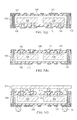
- FIGS. 1( a )-1( c ) illustrate various package structures comprising a substrate with one or more dies embedded in the core layer of the substrates.
- FIGS. 2( a )-2( l ) illustrate a process of manufacturing a substrate with one or more dies embedded in the core layer
- FIGS. 3( a )-3( l ) illustrate another process of manufacturing a substrate with one or more dies embedded in the core layer.
- One or more dies are molded into molding compound to act as a core layer which replaces the normal core layer consisting of dielectric layers of a substrate used in packaging of chips.
- the technique reduces the height of the core layer and shortens the interconnection between chips to achieve high density with lower cost, in addition to better thermal management.
- FIG. 1( a ) illustrates a structure 100 for a core layer of a substrate. It comprises a first die 104 with a die pad 103 , and a molding compound 105 encapsulates the first die 104 while leaving an outer surface of the die pad 103 uncovered by the molding compound, which is in contact with other connection devices such as a via 109 . It further comprises a first dielectric layer 106 on one surface of the molding compound and a second dielectric layer 106 on another surface of the molding compound. A first conductive layer 107 lies on top of the first dielectric layer 106 and a second conductive layer 107 on top of the second dielectric layer 106 , on two sides of the molding compound 105 .
- a hole 108 through the first dielectric layer 106 , the second dielectric layer 106 , and the molding compound 105 is plated or filled with metal 1081 as shown in FIG. 1( a ) or metal plate 1082 as shown in FIG. 1( b ) , where FIG. 1( b ) has all other parts the same as shown in FIG. 1( a ) .
- the description below works for either the hole 108 filled with a metal fill 1081 or plated as a metal plate 1082 . Either the metal fill 1081 or the metal plate 1082 may be used in the following descriptions, which generally work for both cases.
- a laser via 109 is formed through the first dielectric layer 106 and connected to the die pad 103 . There may be more than one vias 109 formed on the structure 100 .
- the metal fill 1081 , the first conductive layer 107 , and the laser via 109 give the structure 100 a generally flat outer surface.
- the structure 100 may connect to the die 211 by the metal fill 1081 in FIG. 1( a ) or the metal plate in FIG. 1( b ) , by way of a connection device such as a solder ball 123 . Additional solder ball 123 may be used to connect the structure 100 to a printed circuit board (not shown) at the opposite side of the die 211 .
- the structure 100 acting as the core layer of the substrate, may be further connected a build up layer 212 as shown in FIG. 1( c ) , where FIG. 1( c ) has all other parts the same as shown in FIG. 1( b ) .
- FIG. 1( c ) shows only a build-up layer on one side of the structure to form the substrate.
- Another build up layer may be formed on another side of the structure to form the substrate (not shown).
- the structure 100 of the core layer of a substrate shown in FIGS. 1( a )-1( c ) are only for illustration purposes and are not limiting. There may be various other configurations performing the same function as the ones shown in FIGS. 1( a )-1( c ) .
- the structure 100 may be simply referred as the core layer of a substrate, or a core layer as well in the following descriptions.
- the first conductive layer 107 and the second conductive layer 107 may be formed on the two sides of the molding compound 105 . They may comprise a plurality of conductive pieces on the same layer where one conductive piece is disconnected from another.
- the first conductive layer 107 may comprise a plurality of conductive sub-layers and the second conductive layer comprise of a plurality of conductive sub-layers.
- the plurality of conductive sub-layers of the first conductive layer and the plurality of conductive sub-layers of the second conductive layer may be formed at different times.
- the material of the conductive layer 107 is not limited.
- the material of the conductive layer is selected from the group consisting of copper, tin, nickel, chromium, titanium, a copper/chromium alloy, and a tin/lead alloy.
- the process for forming the conductive layer 107 is not limited. Preferably, the process is sputtering or electroless plating.
- the process for forming the vias 109 of the dielectric layer 106 is not limited.
- the process is laser-ablation, or exposure and development.
- the laser via 109 may be connected to the metal fill 1081 by way of the first conductive layer 107 .
- An outer surface of the metal fill 1081 , an outer surface of the first conductive layer 107 , and an outer surface of the plurality of laser vias 109 give the structure 100 a flat outer surface.
- a second laser via 109 may be formed through the first dielectric layer 106 and connected to the die pad 103 of the second die 104 .
- the first dielectric layer 106 may be formed a non-photosensitive organic resin, a photosensitive organic resin, such as Ajinomoto Build-up Film (ABF), Benzocyclo-buthene (BCB), Liquid Crystal Polymer (LCP), Poly-imide (PI), Bismaleimide Triazine (BT), Aramide, or other similar materials, and a mixture of epoxy resin and fiber glass.
- a photosensitive organic resin such as Ajinomoto Build-up Film (ABF), Benzocyclo-buthene (BCB), Liquid Crystal Polymer (LCP), Poly-imide (PI), Bismaleimide Triazine (BT), Aramide, or other similar materials, and a mixture of epoxy resin and fiber glass.
- the first conductive layer 107 with the first dielectric layer 106 may be resin coated copper (RCC) or other similar material.
- the second conductive layer 107 with the second dielectric layer 106 may also be RCC or other similar material.
- the buildup layer 212 shown in FIG. 1( c ) may be a build up layer of a PBGA substrate.
- a PBGA substrate comes in a few simple configurations: two layers (2L), four layers (4L) and six layers (6L) of circuitry which are interconnected by plated through holes (PTH). Recently blind holes or vias are also used as interconnects to form substrates with 2L, 1+2+1, 2+2+2 and 1+4+1 layers.
- the structure 100 which acts as a core layer, and the buildup layer 212 shown in FIG. 1( c ) may be for an SBU laminate substrate.
- An SBU laminate substrate may be composed of three distinct technology elements: the surface finish for soldering and adhesion, build-up layers that contain most of the wiring, and a core, which provides mechanical strength.
- Build-up layers are characterized by copper trace dimensions such as width, thickness, and spacing. Almost all signal wiring in SBU occurs in build-up layers.
- FIGS. 2( a )-2( l ) illustrate an example process of manufacturing a structure 100 of a core layer of a substrate with one or more dies 104 embedded in the core layer.
- the method starts at the first step as illustrated in FIG. 2( a ) , where a peelable tape 102 is placed on top of a base 101 covering the base 101 .
- a first die 104 with a die pad 103 is placed on top of the peelable tape 102 while the die pad 103 is in contact with the tape 102 .
- a second die with a die pad may be placed on top of the peelable tape 102 as well while the die pad of the second die is in contact with the tape 102 .
- the number is only for illustration purpose only and there may be more than one or two dies placed on the peelable tape 102 .
- a molding compound 105 is formed on top of the peelable tape 102 and on top of the first die 104 which encapsulates the first die 104 , while leaving the die pad 103 in direct contact with the peelable tape 102 . If there are two dies as illustrated in FIG. 2( c ) , the first die and the second die may be both encapsulated within the molding compound 105 , while the first die and the second die may be separated by the molding compound 105 .
- a first dielectric layer 106 is formed on one surface of the molding compound 105 and a second dielectric layer 106 is formed on another surface of the molding compound 105 .
- a first conductive layer 107 is formed on top of the first dielectric layer 106 and a second metal layer 107 on top of the second dielectric layer 106 .
- the first conductive layer 107 with the first dielectric layer 106 may be resin coated copper (RCC) or other similar material.
- the second conductive layer 107 with the second dielectric layer 106 may be RCC or other similar material.
- the method further proceeds to the next step as shown in FIG. 2( f ) , where a hole or a through hole 108 is drilled through the first dielectric layer 106 , the molding compound 105 , and the second dielectric layer 106 . There may be a multiple holes drilled as well. If the first conductive layer 107 and the first dielectric layer 106 are formed together by RCC material, then the hole may be through the first conductive layer as well.
- the drilled through hole 108 and laser via could be either plating a conductive layer on the surface of drill through hole, or plating conductive layer on the surface of drill through hole and then plug into filling material like resin, or plating conductive copper directly filling the drill through hole, to form a conductive metal plate 1082 .
- one or more laser via 109 are formed through the first dielectric layer connected to the die pad of the first die 104 .
- a laser via through the first dielectric layer connected to the die pad of each of the die may be formed, wherein an outer surface of the metal plate 1082 , an outer surface of the first conductive layer 107 , and an outer surface of the laser via 109 form a flat surface as shown in FIG. 2( f ) .
- a first photo resist film no is attached to the structure 100 covering the metal plate 1082 , the laser via 109 , and the first conductive layer 107 .
- a second photo resist film no covering the metal plate 1082 and the second conductive layer 107 is attached. Illustrated in FIG. 2( h ) , the resist film no is patterned and exposed to etch the first conductive layer 107 on areas not protected by the first resist film no to form the structure shown in FIG. 2( i ) . Similar etching is done for the second conductive layer on areas not protected by the second resist film.
- FIG. 2( j ) illustrates that the first resist film and the second resist film are removed.
- the method then flips the structure to turn the side with via to the up direction so that other dies can be assembled.
- a connection device which may be bumps or solder balls 123 .
- Additional connection device such as solder ball may be used to connect the metal plate to other die or other structures such as PCB, not shown.
- additional structure such as buildup layers may be assembled.
- a build-up layer may cover the metal plate 1082 , the first conductive layer 107 , and the laser via 109 , or assembling another build-up layer covering another side of the structure and the metal fill and the second conductive layer.
- FIGS. 3( a )-3( l ) illustrate another example process of manufacturing a core layer of a substrate with one or more dies embedded in the core layer.
- the method starts at the first step as illustrated in FIG. 3( a ) , where a peelable tape 102 is placed on top of a base 101 covering the base 101 , as previously illustrated in FIG. 2( a ) .
- a first die 104 with a die pad 103 is placed on top of the peelable tape 102 while the die pad 103 is in contact with the tape 102 .
- a second die with a die pad may be placed on top of the peelable tape 102 as well while the die pad of the second die is in contact with the tape 102 .
- the number is only for illustration purpose only and there may be more than one or two dies placed on the peelable tape 102 .
- a molding compound 105 is formed on top of the peelable tape 102 and on top of the first die 104 which encapsulates the first die 104 , while leaving the die pad 103 in direct contact with the surface of the peelable tape 102 . If there are two dies as illustrated in FIG. 3( a ) , the first die and the second die may be both encapsulated within the molding compound 105 , while the first die and the second die may be separated by the molding compound 105 .
- the peelable tape 102 and the base 101 are removed.
- the molding compound 105 surface and the die pad 103 surface form a flat surface which was connected to the base surface.
- the first dielectric layer 106 on both surfaces of the molding compound 105 is formed.
- the first dielectric layer 106 may be formed of a non-photosensitive organic resin, a photosensitive organic resin, such as ABF, BCB, LCP, PI (Poly-imide), BT (Bismaleimide Triazine), or Aramide, and a mixture of epoxy resin and fiber glass, or some other similar materials.
- a through hole 108 which may be called as a hole, is drilled through the first dielectric layer 106 , and the molding compound 105 .
- one or more laser via 109 is formed through the first dielectric layer connected to the die pad 103 of the first die 104 . If there are multiple dies embedded in the molding compound 105 , a laser via through the first dielectric layer connected to the die pad of each of the dies may be formed.
- a first conductive layer 107 is electroless plated on top of the first dielectric layer 106 , on top of the laser via 109 , and on the surface of the through hole 108 to form the metal fill 1081 .
- Components in FIGS. 3( e )-3( f ) which are the same as shown in FIG. 3( d ) are not marked explicitly anymore. However, it is easy to identify those components according to FIG. 3( d ) .
- a first photo resist film no is attached to the structure 100 to cover the surface of the through hole 108 , the laser via 109 , and the first conductive layer 107 on both sides of the structure.
- the resist film no is patterned and exposed in certain areas.
- a second conductive plating 111 may be performed on top of the first conductive layer, but not in the area covered by the resist film no.
- patterned resist film no is removed after the second conductive plating layer 111 is performed.
- fast etch is performed on the first conductive layer 107 and the second conductive layer 111 when the second conductive layer 111 covers up the first conductive layer 107 , to remove the first metal layer 107 on places where only the first metal layer 107 was plated.
- packaged components could be assembled on either side of the substrate.
- An additional die can be assembled to one side of the substrate by bumping, wire bonding, etc.
- Other packaged components like BGA, LGA, capacitor, resistor, etc. could also be assembled on either side of the substrate. What's more, solder ball could be added in one side of the substrate, in order to connect to other substrate or PCB.
- an additional die 211 is connected to the laser via 109 by way of a connection device, which may be 123 bump. There may be a plurality of bumps 123 connecting the vias 109 to the die 211 . Additional connection device such as solder ball 123 may be used to connect the metal fill to other die or other structures such as PCB. Not shown in the figures, additional structure such as buildup layers may be assembled. For example, a build-up layer may cover the metal fill 1081 , the first conductive layer 107 , and the laser via 109 , or assembling another build-up layer covering another side of the structure and the metal fill and the second conductive layer.
Landscapes
- Engineering & Computer Science (AREA)
- Microelectronics & Electronic Packaging (AREA)
- Computer Hardware Design (AREA)
- Power Engineering (AREA)
- Physics & Mathematics (AREA)
- Condensed Matter Physics & Semiconductors (AREA)
- General Physics & Mathematics (AREA)
- Manufacturing & Machinery (AREA)
- Production Of Multi-Layered Print Wiring Board (AREA)
Abstract
A structure for a core layer of a substrate and a method for fabricating a core layer of a substrate are disclosed. The core layer comprises a molding compound encapsulating a die or a plurality of dies, a dielectric layer on the surfaces of the molding compound, and a conductive layer on top of the dielectric layer. A through hole is formed through the dielectric layer and the molding compound, which may be filled with a metal plate. A laser via is formed similarly. Build-up layers may be assembled next to the core layer to form the substrate, which can be used to package dies.
Description
This application is a Divisional of U.S. patent application Ser. No. 13/355,128, filed on Jan. 20, 2012, which application is hereby incorporated herein by reference.
The present invention relates to substrate manufacturing, and in particular embodiments, to systems and methods for substrate manufacturing used in various packaging technologies.
Since the invention of the integrated circuit (IC), the semiconductor industry has experienced rapid growth due to continuous improvements in the integration density of a variety of electronic components. For the most part, this improvement in integration density has come from repeated reductions in minimum feature size, which allows more components to be integrated into a given area. As the demand for even smaller electronic devices has grown, there has grown a need for smaller and more creative packaging techniques of semiconductor dies.
Two types of packaging techniques for die assembly are used. The older and mature technique is wire bonding (WB) where the die is back bonded and wires connect from the top (face) of the die to the substrate. The newer technique is flip chip (FC) bonding, where the chip is bonded face down on the substrate and the interconnection is accomplished with a small solder ball or bump.
There is an increased awareness in the semiconductor industry that assembly and packaging is an essential and integral part of the semiconductor product. Packaging techniques have become a critical competitive factor in many market segments, since it affects operating frequency, power, reliability, and cost. As a result of rapidly emerging technologies and applications, the boundaries between semiconductor, packaging, and system technologies are no longer clear; they must all be considered concurrently in a system-level approach in order to optimize the substrate design and package techniques.
Substrates have become the most expensive element of electronic packages while at the same time limiting package performance. Ceramic, multi-layer substrates have always been very expensive but they allow for a great deal of design freedom e.g. integration of passives. The drawbacks are a high dielectric constant and a very low coefficient of thermal expansion (CTE) as compared to printed circuit boards (PCB) but closely matched to the silicon die. On the other hand, organic substrates have a CTE which is matched to PCBs but is significantly larger than that of the silicon die. Organic substrates were originally introduced to significantly reduce the cost of packaging by taking advantage of low cost PCB manufacturing technology, materials and scale. Organic substrates can be subdivided further, such as laminate substrates used for plastic ball grid array (PBGA), or build-up substrates typically used for Flip Chip die (FCBGA). Sequential build-up (SBU) laminate substrate technology is now the technology of choice for high density, high-performance silicon packaging. For example, SBU technology was selected by Intel for flip-chip packaging.
PBGA substrates come in a few simple configurations: two layers (2L), four layers (4L) and six layers (6L) of circuitry which are interconnected by plated through holes (PTH). An SBU laminate substrate is composed of three distinct technology elements: the surface finish for soldering and adhesion, build-up layers that contain most of the wiring, and a core layer, which provides mechanical strength. How to optimize the core layer design of a substrate for efficient packaging is a problem.
Structures and methods for substrate manufacturing used in various packaging technologies are disclosed. One or more dies are molded into molding compound to act as a core layer which replaces the normal core layer consisting of dielectric layers of a substrate used in packaging of chips. The technique reduces the height of the core layer and shortens the interconnection between chips to achieve high density with lower cost, in addition to better thermal management.
In accordance with an embodiment, a structure for a core layer of a substrate is disclosed. The structure comprises a first die with a die pad, a molding compound encapsulating the first die while leaving an outer surface of the die pad uncovered by the molding compound. A first dielectric layer is further formed on one surface of the molding compound and a second dielectric layer on another surface of the molding compound. A first conductive layer is then formed on top of the first dielectric layer and a second conductive layer on top of the second dielectric layer. A hole is formed through the first dielectric layer, the second dielectric layer, and the molding compound. The hole may be filled with a metal plate. A laser via may be formed through the first dielectric layer and connected to the die pad. The laser via may be connected to the metal plate by way of the first conductive layer.
In accordance with an embodiment, a structure for a core layer of a substrate is disclosed. A build-up layer may be formed on one side of the structure for the core layer to form a substrate. Another build up layer on another side of the structure for the core layer to form the substrate. An additional die may be connected to the laser via of the structure of the core layer by way of a connection device. An additional die may be connected to the metal plate by way of a connection device.
In accordance with an embodiment, the structure for a core layer of a substrate may further comprise a plurality of die pads for the first die, and a plurality of laser vias through the first conductive layer and the first dielectric layer connected to the plurality of die pads. The structure for a core layer of a substrate may further comprise a plurality of holes through the first dielectric layer, the second dielectric layer, and the molding compound, which are filled with a plurality of metal plates.
In accordance with an embodiment, the structure for a core layer of a substrate may further comprise a second die with a die pad, where the molding compound encapsulates the second die separated from the first die. A second laser via through the first conductive layer and the first dielectric layer is connected to the die pad of the second die.
In accordance with an embodiment, the structure for a core layer of a substrate may have the first dielectric layer made of Ajinomoto Build-up Film (ABF), Benzocyclo-buthene (BCB), or other similar material. The first conductive layer with the first dielectric layer and the second conductive layer with the second dielectric layer may comprise of resin coated copper (RCC) or other similar material. The first conductive layer may comprise a plurality of conductive sub-layers and the second conductive layer may comprise a plurality of conductive sub-layers. The plurality of conductive sub-layers of the first conductive layer and the plurality of conductive sub-layers of the second conductive layer may be formed at different times.
In accordance with an example embodiment, a method for fabricating a core layer of a substrate is provided. The method places a first die with a die pad on top of a peelable tape covering a base while the die pad is in contact with the tape. A second die with a die pad may be similarly placed. The method then encapsulates the first die and the die pad using a molding compound, after which the base and the peelable tape may be removed. The second die may be similarly encapsulated. The method then forms a first dielectric layer on one surface of the molding compound and a second dielectric layer on another surface of the molding compound, and forms a first conductive layer on top of the first dielectric layer and a second conductive layer on top of the second dielectric layer. The method further forms a hole through the first conductive layer, the second conductive layer, the first dielectric layer, the second dielectric layer, and the molding compound. A laser via may be similarly formed through the first conductive layer and the first dielectric layer connected to the die pad of the encapsulated dies. The method then plates the hole and laser via with a metal plate. The method further attaches a first photo resist film covering the metal plate, the laser via, and the first conductive layer, and attaches a second photo resist film covering the metal plate and the second conductive layer. A pattern is formed by etching the first conductive layer on areas not protected by the first resist film, and etching the second conductive layer on areas not protected by the second resist film. Finally, the first resist film and the second resist film are removed.
In accordance with an example embodiment, a method for fabricating a core layer of a substrate is provided. A build-up layer may be assembled to cover the metal plate, the first conductive layer, and the laser via of the core layer. Another build-up layer may be assembled to cover the metal plate and the second conductive layer.
In accordance with an example embodiment, a method for fabricating a core layer of a substrate is provided. The method comprises placing a first die with a die pad on top of a peelable tape covering a base while the die pad is in contact with the tape, forming a molding compound on top of the peelable tape and on top of the first die which encapsulates the first die, removing the base and the peelable tape, forming a first dielectric layer on one surface of the molding compound and a second dielectric layer on another surface of the molding compound, forming a through hole through the first dielectric layer, the second dielectric layer, and the molding compound, drilling a via through the first dielectric layer connected to the die pad of the first die, electroless plating a first conductive layer over the first dielectric layer, the second dielectric layer, the through hole, and the via, attaching a resist film covering the electroless plated first conductive layer, patterning and exposing the resist film to form a pattern, plating a second conductive layer over the through hole, the via, and over the first conductive layer which are over the first dielectric layer and the second dielectric layer based on the pattern of the resist film, removing the resist film, and etching the first conductive layer and the second conductive layer to remove the first conductive layer on places where only the first conductive layer is plated.
For a more complete understanding of the present disclosure, and the advantages thereof, reference is now made to the following descriptions taken in conjunction with the accompanying drawings, in which:
Corresponding numerals and symbols in the different figures generally refer to corresponding parts unless otherwise indicated. The figures are drawn to clearly illustrate the relevant aspects of the various embodiments and are not necessarily drawn to scale.
The making and using of the embodiments of the present disclosure are discussed in details below. It should be appreciated, however, that the embodiments of the present disclosure provide many applicable concepts that can be embodied in a wide variety of specific contexts. The specific embodiments discussed are merely illustrative of specific ways to make and use the disclosure, and do not limit the scope of the disclosure.
As will be more fully explained below, structures and methods for substrate manufacturing used in various packaging technologies will be disclosed. One or more dies are molded into molding compound to act as a core layer which replaces the normal core layer consisting of dielectric layers of a substrate used in packaging of chips. The technique reduces the height of the core layer and shortens the interconnection between chips to achieve high density with lower cost, in addition to better thermal management.
A laser via 109 is formed through the first dielectric layer 106 and connected to the die pad 103. There may be more than one vias 109 formed on the structure 100. The metal fill 1081, the first conductive layer 107, and the laser via 109 give the structure 100 a generally flat outer surface. An additional die 211 connected to the laser vias 109 through a plurality of solder balls 123. The structure 100 may connect to the die 211 by the metal fill 1081 in FIG. 1(a) or the metal plate in FIG. 1(b) , by way of a connection device such as a solder ball 123. Additional solder ball 123 may be used to connect the structure 100 to a printed circuit board (not shown) at the opposite side of the die 211.
Furthermore, the structure 100, acting as the core layer of the substrate, may be further connected a build up layer 212 as shown in FIG. 1(c) , where FIG. 1(c) has all other parts the same as shown in FIG. 1(b) . FIG. 1(c) shows only a build-up layer on one side of the structure to form the substrate. Another build up layer may be formed on another side of the structure to form the substrate (not shown).
The structure 100 of the core layer of a substrate shown in FIGS. 1(a)-1(c) are only for illustration purposes and are not limiting. There may be various other configurations performing the same function as the ones shown in FIGS. 1(a)-1(c) . The structure 100 may be simply referred as the core layer of a substrate, or a core layer as well in the following descriptions.
The first conductive layer 107 and the second conductive layer 107 may be formed on the two sides of the molding compound 105. They may comprise a plurality of conductive pieces on the same layer where one conductive piece is disconnected from another. The first conductive layer 107 may comprise a plurality of conductive sub-layers and the second conductive layer comprise of a plurality of conductive sub-layers. The plurality of conductive sub-layers of the first conductive layer and the plurality of conductive sub-layers of the second conductive layer may be formed at different times.
The material of the conductive layer 107 is not limited. Preferably, the material of the conductive layer is selected from the group consisting of copper, tin, nickel, chromium, titanium, a copper/chromium alloy, and a tin/lead alloy. The process for forming the conductive layer 107 is not limited. Preferably, the process is sputtering or electroless plating.
The process for forming the vias 109 of the dielectric layer 106 is not limited. Preferably, the process is laser-ablation, or exposure and development. The laser via 109 may be connected to the metal fill 1081 by way of the first conductive layer 107.
There may be more than one die pad 103 for the first die 104, and more than one laser via 109 through the first dielectric layer 106 connected to the plurality of die pads 103. An outer surface of the metal fill 1081, an outer surface of the first conductive layer 107, and an outer surface of the plurality of laser vias 109 give the structure 100 a flat outer surface.
There may be more than one hole 108 through the first dielectric layer 106, the second dielectric layer 106, and the molding compound 105, which are filled with a plurality of metal fills 1081, wherein outer surfaces of the plurality of metal fill 1081 and an outer surface of the first conductive layer 107 give the structure 100 a flat outer surface.
There may be more than one dies 104 each with a die pad 103, where the molding compound 105 encapsulates the second die apart from the first die while leaving an outer surface of the die pad of the second die uncovered by the molding compound, as shown in FIG. 1(a) . A second laser via 109 may be formed through the first dielectric layer 106 and connected to the die pad 103 of the second die 104.
The first dielectric layer 106 may be formed a non-photosensitive organic resin, a photosensitive organic resin, such as Ajinomoto Build-up Film (ABF), Benzocyclo-buthene (BCB), Liquid Crystal Polymer (LCP), Poly-imide (PI), Bismaleimide Triazine (BT), Aramide, or other similar materials, and a mixture of epoxy resin and fiber glass.
The first conductive layer 107 with the first dielectric layer 106 may be resin coated copper (RCC) or other similar material. The second conductive layer 107 with the second dielectric layer 106 may also be RCC or other similar material.
The buildup layer 212 shown in FIG. 1(c) may be a build up layer of a PBGA substrate. A PBGA substrate comes in a few simple configurations: two layers (2L), four layers (4L) and six layers (6L) of circuitry which are interconnected by plated through holes (PTH). Recently blind holes or vias are also used as interconnects to form substrates with 2L, 1+2+1, 2+2+2 and 1+4+1 layers.
The structure 100, which acts as a core layer, and the buildup layer 212 shown in FIG. 1(c) may be for an SBU laminate substrate. An SBU laminate substrate may be composed of three distinct technology elements: the surface finish for soldering and adhesion, build-up layers that contain most of the wiring, and a core, which provides mechanical strength. Build-up layers are characterized by copper trace dimensions such as width, thickness, and spacing. Almost all signal wiring in SBU occurs in build-up layers.
The method starts at the first step as illustrated in FIG. 2(a) , where a peelable tape 102 is placed on top of a base 101 covering the base 101. In FIG. 2(b) , a first die 104 with a die pad 103 is placed on top of the peelable tape 102 while the die pad 103 is in contact with the tape 102. A second die with a die pad may be placed on top of the peelable tape 102 as well while the die pad of the second die is in contact with the tape 102. The number is only for illustration purpose only and there may be more than one or two dies placed on the peelable tape 102.
In FIG. 2(c) , a molding compound 105 is formed on top of the peelable tape 102 and on top of the first die 104 which encapsulates the first die 104, while leaving the die pad 103 in direct contact with the peelable tape 102. If there are two dies as illustrated in FIG. 2(c) , the first die and the second die may be both encapsulated within the molding compound 105, while the first die and the second die may be separated by the molding compound 105.
The descriptions below are for one example die 104 embedded in the molding compound 105. However, the procedures can be carried out similarly for multiple embedded dies within the molding compound 105.
In FIG. 2(d) , the peelable tape 102 and the base 101 are removed, so that the molding compound 105 surface and the die pad 103 surface form a flat surface which was connected to the tape surface. In FIG. 2(e) , a first dielectric layer 106 is formed on one surface of the molding compound 105 and a second dielectric layer 106 is formed on another surface of the molding compound 105. A first conductive layer 107 is formed on top of the first dielectric layer 106 and a second metal layer 107 on top of the second dielectric layer 106. The first conductive layer 107 with the first dielectric layer 106 may be resin coated copper (RCC) or other similar material. The second conductive layer 107 with the second dielectric layer 106 may be RCC or other similar material.
The method further proceeds to the next step as shown in FIG. 2(f) , where a hole or a through hole 108 is drilled through the first dielectric layer 106, the molding compound 105, and the second dielectric layer 106. There may be a multiple holes drilled as well. If the first conductive layer 107 and the first dielectric layer 106 are formed together by RCC material, then the hole may be through the first conductive layer as well.
Next the drilled through hole 108 and laser via could be either plating a conductive layer on the surface of drill through hole, or plating conductive layer on the surface of drill through hole and then plug into filling material like resin, or plating conductive copper directly filling the drill through hole, to form a conductive metal plate 1082. Similarly, one or more laser via 109 are formed through the first dielectric layer connected to the die pad of the first die 104. If there are multiple dies embedded in the molding compound 105, a laser via through the first dielectric layer connected to the die pad of each of the die may be formed, wherein an outer surface of the metal plate 1082, an outer surface of the first conductive layer 107, and an outer surface of the laser via 109 form a flat surface as shown in FIG. 2(f) .
As illustrated in FIG. 2(g) , a first photo resist film no is attached to the structure 100 covering the metal plate 1082, the laser via 109, and the first conductive layer 107. Similarly a second photo resist film no covering the metal plate 1082 and the second conductive layer 107 is attached. Illustrated in FIG. 2(h) , the resist film no is patterned and exposed to etch the first conductive layer 107 on areas not protected by the first resist film no to form the structure shown in FIG. 2(i) . Similar etching is done for the second conductive layer on areas not protected by the second resist film. FIG. 2(j) illustrates that the first resist film and the second resist film are removed.
As illustrated in FIG. 2(k) , the method then flips the structure to turn the side with via to the up direction so that other dies can be assembled. Illustrated in FIG. 2(l) , an additional die 211 is connected to the laser via 109 by way of a connection device, which may be bumps or solder balls 123. There may be a plurality of bumps 123 connecting the vias 109 to the die 211. Additional connection device such as solder ball may be used to connect the metal plate to other die or other structures such as PCB, not shown. Not shown in the figures, additional structure such as buildup layers may be assembled. For example, a build-up layer may cover the metal plate 1082, the first conductive layer 107, and the laser via 109, or assembling another build-up layer covering another side of the structure and the metal fill and the second conductive layer.
The method starts at the first step as illustrated in FIG. 3(a) , where a peelable tape 102 is placed on top of a base 101 covering the base 101, as previously illustrated in FIG. 2(a) . A first die 104 with a die pad 103 is placed on top of the peelable tape 102 while the die pad 103 is in contact with the tape 102. A second die with a die pad may be placed on top of the peelable tape 102 as well while the die pad of the second die is in contact with the tape 102. The number is only for illustration purpose only and there may be more than one or two dies placed on the peelable tape 102. A molding compound 105 is formed on top of the peelable tape 102 and on top of the first die 104 which encapsulates the first die 104, while leaving the die pad 103 in direct contact with the surface of the peelable tape 102. If there are two dies as illustrated in FIG. 3(a) , the first die and the second die may be both encapsulated within the molding compound 105, while the first die and the second die may be separated by the molding compound 105.
The descriptions below are for one example die 104 embedded in the molding compound 105. However, the procedures can be carried out similarly for multiple embedded dies within the molding compound 105.
In FIG. 3(b) , the peelable tape 102 and the base 101 are removed. As such, the molding compound 105 surface and the die pad 103 surface form a flat surface which was connected to the base surface.
In FIG. 3(c) , a first dielectric layer 106 on both surfaces of the molding compound 105 is formed. The first dielectric layer 106 may be formed of a non-photosensitive organic resin, a photosensitive organic resin, such as ABF, BCB, LCP, PI (Poly-imide), BT (Bismaleimide Triazine), or Aramide, and a mixture of epoxy resin and fiber glass, or some other similar materials.
In FIG. 3(d) , a through hole 108, which may be called as a hole, is drilled through the first dielectric layer 106, and the molding compound 105. Similarly, one or more laser via 109 is formed through the first dielectric layer connected to the die pad 103 of the first die 104. If there are multiple dies embedded in the molding compound 105, a laser via through the first dielectric layer connected to the die pad of each of the dies may be formed.
In FIG. 3(e) , a first conductive layer 107 is electroless plated on top of the first dielectric layer 106, on top of the laser via 109, and on the surface of the through hole 108 to form the metal fill 1081. Components in FIGS. 3(e)-3(f) which are the same as shown in FIG. 3(d) are not marked explicitly anymore. However, it is easy to identify those components according to FIG. 3(d) .
As illustrated in FIG. 3(f) , a first photo resist film no is attached to the structure 100 to cover the surface of the through hole 108, the laser via 109, and the first conductive layer 107 on both sides of the structure.
Illustrated in FIG. 3(g) , the resist film no is patterned and exposed in certain areas. Illustrated in FIG. 3(h) , a second conductive plating 111 may be performed on top of the first conductive layer, but not in the area covered by the resist film no.
Illustrated in FIG. 3(i) , patterned resist film no is removed after the second conductive plating layer 111 is performed.
Illustrated in FIG. 3(j) , fast etch is performed on the first conductive layer 107 and the second conductive layer 111 when the second conductive layer 111 covers up the first conductive layer 107, to remove the first metal layer 107 on places where only the first metal layer 107 was plated.
Illustrated in FIG. 3(k) , other dies, packaged components could be assembled on either side of the substrate. An additional die can be assembled to one side of the substrate by bumping, wire bonding, etc. Other packaged components (like BGA, LGA, capacitor, resistor, etc.) could also be assembled on either side of the substrate. What's more, solder ball could be added in one side of the substrate, in order to connect to other substrate or PCB.
Illustrated in FIG. 3(l) , an additional die 211 is connected to the laser via 109 by way of a connection device, which may be 123 bump. There may be a plurality of bumps 123 connecting the vias 109 to the die 211. Additional connection device such as solder ball 123 may be used to connect the metal fill to other die or other structures such as PCB. Not shown in the figures, additional structure such as buildup layers may be assembled. For example, a build-up layer may cover the metal fill 1081, the first conductive layer 107, and the laser via 109, or assembling another build-up layer covering another side of the structure and the metal fill and the second conductive layer.
Although the present disclosure and its advantages have been described in detail, it should be understood that various changes, substitutions and alterations can be made herein without departing from the spirit and scope of the invention as defined by the appended claims. Moreover, the scope of the present application is not intended to be limited to the particular embodiments of the process, machine, manufacture, and composition of matter, means, methods and steps described in the specification. As one of ordinary skill in the art will readily appreciate from the present disclosure, processes, machines, manufacture, compositions of matter, means, methods, or steps, presently existing or later to be developed, that perform substantially the same function or achieve substantially the same result as the corresponding embodiments described herein may be utilized according to the present disclosure. Accordingly, the appended claims are intended to include within their scope such processes, machines, manufacture, compositions of matter, means, methods, or steps. In addition, each claim constitutes a separate embodiment, and the combination of various claims and embodiments are within the scope of the invention.
Claims (20)
1. A method for fabricating a core layer of a substrate, comprising:
placing a first die with a die pad on top of a peelable tape covering a base while the die pad is in contact with the peelable tape;
encapsulating the first die and the die pad using a molding compound;
removing the base and the peelable tape after the encapsulating;
forming a first dielectric layer on one surface of the molding compound and a second dielectric layer on another surface of the molding compound after removing the base and the peelable tape;
forming a first conductive layer on top of the first dielectric layer and a second conductive layer on top of the second dielectric layer;
forming a through hole through the first conductive layer, the second conductive layer, the first dielectric layer, the second dielectric layer, and the molding compound after forming the first and second conductive layers;
forming a laser via through the first conductive layer and the first dielectric layer connected to the die pad of the first die after forming the first and second conductive layers;
plating the through hole and laser via with a metal plate, a flat surface being formed by an outer surface of the metal plate, an outer surface of the first conductive layer, and an outer surface of the laser via;
attaching a first photo resist film covering the metal plate, the laser via, and the first conductive layer;
attaching a second photo resist film covering the metal plate and the second conductive layer;
etching the first conductive layer on areas not protected by the first photo resist film;
etching the second conductive layer on areas not protected by the second photo resist film; and
removing the first photo resist film and the second photo resist film.
2. The method of claim 1 , further comprising assembling a build-up layer covering the metal plate, the first conductive layer, and the laser via.
3. The method of claim 1 , further comprising assembling a build-up layer covering the metal plate and the second conductive layer.
4. The method of claim 1 , further comprising:
placing a second die with a die pad on top of the peelable tape covering the base while the die pad of the second die is in contact with the peelable tape;
forming the molding compound on top of the peelable tape, the first die, and the second die, which encapsulates the first die and the second die while separating the first die and the second die by the molding compound; and
forming a second laser via through the first conductive layer and the first dielectric layer connected to the die pad of the second die.
5. The method of claim 1 , further comprising attaching the die pads of the first and second dies to respective bumps of a third die.
6. The method of claim 1 , the first dielectric layer and the first conductive layer collectively, and the second dielectric layer and the second conductive layer collectively, each comprising resin coated copper.
7. A method for fabricating a core layer of a substrate, comprising:
placing a first die with a die pad on top of a peelable tape covering a base while the die pad is in contact with the peelable tape;
encapsulating the first die and the die pad using a molding compound;
removing the base and the peelable tape;
forming a first dielectric layer on one surface of the molding compound and a second dielectric layer on another surface of the molding compound opposite the one surface;
forming a first conductive layer on top of the first dielectric layer and a second conductive layer on top of the second dielectric layer;
forming a through hole through the first conductive layer, the second conductive layer, the first dielectric layer, the second dielectric layer, and the molding compound;
forming a laser via through the first conductive layer and the first dielectric layer connected to the die pad of the first die; and
plating the through hole and laser via with a metal conductor.
8. The method of claim 7 , further comprising:
attaching a first photo resist film covering the metal conductor, the laser via, and the first conductive layer;
attaching a second photo resist film covering the metal conductor and the second conductive layer;
etching the first conductive layer on areas not protected by the first photo resist film;
etching the second conductive layer on areas not protected by the second photo resist film; and
removing the first photo resist film and the second photo resist film.
9. The method of claim 8 , further comprising assembling a build-up layer covering the metal conductor, the first conductive layer, and the laser via.
10. The method of claim 8 , further comprising assembling a build-up layer covering the metal conductor and the second conductive layer.
11. The method of claim 8 , further comprising:
placing a second die with a die pad on top of the peelable tape covering the base while the die pad of the second die is in contact with the peelable tape;
forming the molding compound on top of the peelable tape, the first die, and the second die, which encapsulates the first die and the second die while separating the first die and the second die by the molding compound; and
forming a second laser via through the first conductive layer and the first dielectric layer connected to the die pad of the second die.
12. The method of claim 11 , further comprising attaching the die pads of the first and second dies to respective bumps of a third die.
13. The method of claim 7 , the first dielectric layer and the first conductive layer collectively, and the second dielectric layer and the second conductive layer collectively, each comprising resin coated copper.
14. A method for fabricating a core layer of a substrate, comprising:
placing a first die with a die pad on top of a peelable tape covering a base while the die pad is in contact with the peelable tape;
forming a molding compound on top of the peelable tape and on top of the first die to encapsulate the first die;
removing the base and the peelable tape;
forming a first dielectric layer on one surface of the molding compound and a second dielectric layer on another surface of the molding compound opposite the one surface;
forming a through hole through the first dielectric layer, the second dielectric layer, and the molding compound;
drilling a via through the first dielectric layer connected to the die pad of the first die;
electroless plating a first conductive layer over the first dielectric layer, the second dielectric layer, the through hole, and the via;
attaching a resist film covering the electroless plated first conductive layer;
patterning and exposing the resist film to form a pattern;
plating a second conductive layer over the through hole, the via, and over the first conductive layer which are over the first dielectric layer and the second dielectric layer, based on the pattern of the resist film;
removing the resist film; and
etching the first conductive layer and the second conductive layer to remove the first conductive layer only from areas where the first conductive layer is plated.
15. The method of claim 14 , further comprising assembling a build-up layer covering the second conductive layer.
16. The method of claim 14 , further comprising:
placing a second die with a second die pad on top of the peelable tape covering the base while the second die pad is in contact with the peelable tape;
forming the molding compound on top of the peelable tape, the first die and the second die to encapsulate the first die and the second die, while separating the first die and the second die by the molding compound; and
drilling a second via through the first dielectric layer connected to the second die pad.
17. The method of claim 16 , further comprising attaching the die pads of the first and second dies to respective bumps of a third die.
18. The method of claim 14 , the first and second dielectric layers each comprising a material selected from the group consisting of: build-up film, benzocyclo-buthene, liquid crystal polymer, poly-imide, bismaleimide triazine, and Aramide.
19. The method of claim 14 , the first and second conductive layers each comprising a material selected from the group consisting of: copper, tin, nickel, chromium, titanium, a copper/chromium alloy, and a tin/lead alloy.
20. The method of claim 14 , the first dielectric layer and the first conductive layer collectively, and the second dielectric layer and the second conductive layer collectively, each comprising resin coated copper.
Priority Applications (1)
| Application Number | Priority Date | Filing Date | Title |
|---|---|---|---|
| US16/001,416 US10212818B2 (en) | 2012-01-20 | 2018-06-06 | Methods and apparatus for a substrate core layer |
Applications Claiming Priority (2)
| Application Number | Priority Date | Filing Date | Title |
|---|---|---|---|
| US13/355,128 US20130186676A1 (en) | 2012-01-20 | 2012-01-20 | Methods and Apparatus for a Substrate Core Layer |
| US16/001,416 US10212818B2 (en) | 2012-01-20 | 2018-06-06 | Methods and apparatus for a substrate core layer |
Related Parent Applications (1)
| Application Number | Title | Priority Date | Filing Date |
|---|---|---|---|
| US13/355,128 Division US20130186676A1 (en) | 2012-01-20 | 2012-01-20 | Methods and Apparatus for a Substrate Core Layer |
Publications (2)
| Publication Number | Publication Date |
|---|---|
| US20180288880A1 US20180288880A1 (en) | 2018-10-04 |
| US10212818B2 true US10212818B2 (en) | 2019-02-19 |
Family
ID=48796318
Family Applications (2)
| Application Number | Title | Priority Date | Filing Date |
|---|---|---|---|
| US13/355,128 Abandoned US20130186676A1 (en) | 2012-01-20 | 2012-01-20 | Methods and Apparatus for a Substrate Core Layer |
| US16/001,416 Active US10212818B2 (en) | 2012-01-20 | 2018-06-06 | Methods and apparatus for a substrate core layer |
Family Applications Before (1)
| Application Number | Title | Priority Date | Filing Date |
|---|---|---|---|
| US13/355,128 Abandoned US20130186676A1 (en) | 2012-01-20 | 2012-01-20 | Methods and Apparatus for a Substrate Core Layer |
Country Status (5)
| Country | Link |
|---|---|
| US (2) | US20130186676A1 (en) |
| EP (1) | EP2798675B1 (en) |
| JP (1) | JP5932056B2 (en) |
| CN (1) | CN104428892B (en) |
| WO (1) | WO2013107406A1 (en) |
Cited By (1)
| Publication number | Priority date | Publication date | Assignee | Title |
|---|---|---|---|---|
| US11610851B2 (en) | 2020-04-29 | 2023-03-21 | Stmicroelectronics, Inc. | Die embedded in substrate with stress buffer |
Families Citing this family (17)
| Publication number | Priority date | Publication date | Assignee | Title |
|---|---|---|---|---|
| US10050004B2 (en) * | 2015-11-20 | 2018-08-14 | Deca Technologies Inc. | Fully molded peripheral package on package device |
| US8952533B2 (en) * | 2012-09-10 | 2015-02-10 | Futurewei Technologies, Inc. | Devices and methods for 2.5D interposers |
| US8901748B2 (en) * | 2013-03-14 | 2014-12-02 | Intel Corporation | Direct external interconnect for embedded interconnect bridge package |
| JP6320681B2 (en) * | 2013-03-29 | 2018-05-09 | ローム株式会社 | Semiconductor device |
| US9831189B2 (en) * | 2013-07-09 | 2017-11-28 | Nvidia Corporation | Integrated circuit package with a conductive grid formed in a packaging substrate |
| US9488779B2 (en) * | 2013-11-11 | 2016-11-08 | Taiwan Semiconductor Manufacturing Company, Ltd. | Apparatus and method of forming laser chip package with waveguide for light coupling |
| CN104851868B (en) * | 2014-02-14 | 2017-08-11 | 恒劲科技股份有限公司 | Packaging system and preparation method thereof |
| CN104851869B (en) * | 2014-02-14 | 2017-09-22 | 恒劲科技股份有限公司 | Packaging system and preparation method thereof |
| US9330994B2 (en) * | 2014-03-28 | 2016-05-03 | Stats Chippac, Ltd. | Semiconductor device and method of forming RDL and vertical interconnect by laser direct structuring |
| JP2016213372A (en) * | 2015-05-12 | 2016-12-15 | 日立化成株式会社 | Semiconductor device and method of manufacturing the same |
| JP6569288B2 (en) * | 2015-05-12 | 2019-09-04 | 日立化成株式会社 | Semiconductor device and manufacturing method of semiconductor device |
| US10090241B2 (en) * | 2015-05-29 | 2018-10-02 | Taiwan Semiconductor Manufacturing Co., Ltd. | Device, package structure and method of forming the same |
| CN106851983A (en) * | 2017-03-28 | 2017-06-13 | 华为技术有限公司 | Board structure of circuit with embedment device and preparation method thereof |
| US10672729B2 (en) * | 2017-03-30 | 2020-06-02 | Taiwan Semiconductor Manufacturing Co., Ltd. | Package structure and method of forming package structure |
| US10269773B1 (en) | 2017-09-29 | 2019-04-23 | Taiwan Semiconductor Manufacturing Company, Ltd. | Semiconductor packages and methods of forming the same |
| US10405421B2 (en) | 2017-12-18 | 2019-09-03 | International Business Machines Corporation | Selective dielectric resin application on circuitized core layers |
| US20220122936A1 (en) * | 2020-10-20 | 2022-04-21 | Texas Instruments Incorporated | Enhanced mold compound thermal conductivity |
Citations (16)
| Publication number | Priority date | Publication date | Assignee | Title |
|---|---|---|---|---|
| US20040107569A1 (en) * | 2002-12-05 | 2004-06-10 | John Guzek | Metal core substrate packaging |
| US20050001331A1 (en) * | 2003-07-03 | 2005-01-06 | Toshiyuki Kojima | Module with a built-in semiconductor and method for producing the same |
| JP2005209933A (en) | 2004-01-23 | 2005-08-04 | Nec Electronics Corp | Multilayer wiring substrate, semiconductor device, and manufacturing method of them |
| DE102006001429A1 (en) | 2006-01-10 | 2007-03-22 | Infineon Technologies Ag | Semiconductor component functional unit and production process has rows and columns of chips on a connection plate and a multi-layer wiring structure insulated by a hybrid organic-inorganic polymer dielectric |
| US20070069353A1 (en) * | 2005-09-23 | 2007-03-29 | Gottfried Beer | Semiconductor device with plastic housing composition and method for producing the same |
| US20080136009A1 (en) * | 2006-12-08 | 2008-06-12 | Horst Theuss | Semiconductor device with hollow structure |
| US20080237879A1 (en) * | 2007-03-30 | 2008-10-02 | Wen-Kun Yang | Semiconductor device package with die receiving through-hole and dual build-up layers over both side-surfaces for wlp and method of the same |
| US20080237828A1 (en) * | 2007-03-30 | 2008-10-02 | Advanced Chip Engineering Technology Inc. | Semiconductor device package with die receiving through-hole and dual build-up layers over both side-surfaces for wlp and method of the same |
| US20090155956A1 (en) * | 2007-07-02 | 2009-06-18 | Infineon Technologies Ag | Semiconductor device |
| US20100019370A1 (en) * | 2008-07-24 | 2010-01-28 | Infineon Technologies Ag | Semiconductor device and manufacturing method |
| US20100053920A1 (en) * | 2008-09-02 | 2010-03-04 | Unimicron Technology Corporation | Packaging substrate with embedded semiconductor component and method for fabricating the same |
| US20100133682A1 (en) * | 2008-12-02 | 2010-06-03 | Infineon Technologies Ag | Semiconductor device |
| US20100314352A1 (en) * | 2009-06-12 | 2010-12-16 | Unimicron Technology Corp. | Fabricating method of embedded package structure |
| US20110001247A1 (en) * | 2009-07-01 | 2011-01-06 | Casio Computer Co., Ltd. | Semiconductor device manufacturing method |
| US20110221054A1 (en) * | 2010-03-15 | 2011-09-15 | Stats Chippac, Ltd. | Semiconductor Device and Method of Forming Conductive Vias Through Interconnect Structures and Encapsulant of WLCSP |
| JP2011211242A (en) | 2009-12-14 | 2011-10-20 | Sumitomo Bakelite Co Ltd | Method for producing electronic device, electronic device, method for producing electronic device package, and electronic device package |
-
2012
- 2012-01-20 US US13/355,128 patent/US20130186676A1/en not_active Abandoned
-
2013
- 2013-01-21 CN CN201380006004.4A patent/CN104428892B/en active Active
- 2013-01-21 WO PCT/CN2013/070756 patent/WO2013107406A1/en active Application Filing
- 2013-01-21 EP EP13738161.2A patent/EP2798675B1/en active Active
- 2013-01-21 JP JP2014552504A patent/JP5932056B2/en active Active
-
2018
- 2018-06-06 US US16/001,416 patent/US10212818B2/en active Active
Patent Citations (22)
| Publication number | Priority date | Publication date | Assignee | Title |
|---|---|---|---|---|
| US20040107569A1 (en) * | 2002-12-05 | 2004-06-10 | John Guzek | Metal core substrate packaging |
| CN1720617A (en) | 2002-12-05 | 2006-01-11 | 英特尔公司 | Metal core substrate packaging |
| US20050001331A1 (en) * | 2003-07-03 | 2005-01-06 | Toshiyuki Kojima | Module with a built-in semiconductor and method for producing the same |
| JP2005209933A (en) | 2004-01-23 | 2005-08-04 | Nec Electronics Corp | Multilayer wiring substrate, semiconductor device, and manufacturing method of them |
| US20070069353A1 (en) * | 2005-09-23 | 2007-03-29 | Gottfried Beer | Semiconductor device with plastic housing composition and method for producing the same |
| DE102006001429A1 (en) | 2006-01-10 | 2007-03-22 | Infineon Technologies Ag | Semiconductor component functional unit and production process has rows and columns of chips on a connection plate and a multi-layer wiring structure insulated by a hybrid organic-inorganic polymer dielectric |
| US20080136009A1 (en) * | 2006-12-08 | 2008-06-12 | Horst Theuss | Semiconductor device with hollow structure |
| CN101325188A (en) | 2007-03-30 | 2008-12-17 | 育霈科技股份有限公司 | Wafer level semiconductor package with dual side build-up layers and method thereof |
| JP2008258621A (en) | 2007-03-30 | 2008-10-23 | Advanced Chip Engineering Technology Inc | Semiconductor device package structure and formation method thereof |
| US20080237879A1 (en) * | 2007-03-30 | 2008-10-02 | Wen-Kun Yang | Semiconductor device package with die receiving through-hole and dual build-up layers over both side-surfaces for wlp and method of the same |
| US20080237828A1 (en) * | 2007-03-30 | 2008-10-02 | Advanced Chip Engineering Technology Inc. | Semiconductor device package with die receiving through-hole and dual build-up layers over both side-surfaces for wlp and method of the same |
| US20090155956A1 (en) * | 2007-07-02 | 2009-06-18 | Infineon Technologies Ag | Semiconductor device |
| US8779583B2 (en) * | 2008-07-24 | 2014-07-15 | Infineon Technologies Ag | Semiconductor device and manufacturing method |
| US20100019370A1 (en) * | 2008-07-24 | 2010-01-28 | Infineon Technologies Ag | Semiconductor device and manufacturing method |
| US20100053920A1 (en) * | 2008-09-02 | 2010-03-04 | Unimicron Technology Corporation | Packaging substrate with embedded semiconductor component and method for fabricating the same |
| US20100133682A1 (en) * | 2008-12-02 | 2010-06-03 | Infineon Technologies Ag | Semiconductor device |
| US20100314352A1 (en) * | 2009-06-12 | 2010-12-16 | Unimicron Technology Corp. | Fabricating method of embedded package structure |
| US20110001247A1 (en) * | 2009-07-01 | 2011-01-06 | Casio Computer Co., Ltd. | Semiconductor device manufacturing method |
| JP2011029602A (en) | 2009-07-01 | 2011-02-10 | Casio Computer Co Ltd | Semiconductor device and manufacturing method thereof |
| JP2011211242A (en) | 2009-12-14 | 2011-10-20 | Sumitomo Bakelite Co Ltd | Method for producing electronic device, electronic device, method for producing electronic device package, and electronic device package |
| EP2515329A1 (en) | 2009-12-14 | 2012-10-24 | Sumitomo Bakelite Co., Ltd. | Method for producing electronic device, electronic device, method for producing electronic device package, and electronic device package |
| US20110221054A1 (en) * | 2010-03-15 | 2011-09-15 | Stats Chippac, Ltd. | Semiconductor Device and Method of Forming Conductive Vias Through Interconnect Structures and Encapsulant of WLCSP |
Non-Patent Citations (3)
| Title |
|---|
| "Copper (Cu) Wire Bonding," Amkor Technology retrieved from www.amkor.com, Jan. 20, 2012, 2 pages. |
| Braun, T., et al., "Through Mold Vias for Stacking of Mold Embedded Packages," Electronic Components and Technology Conference, IEEE Std. 978, 2011, pp. 48-54. |
| Ramm, P. et al., "3D System Integration Technologies," Materials Research Society Symposium Proc., vol. 766, 2003, pp. E5.6.1-E5.6.12. |
Cited By (1)
| Publication number | Priority date | Publication date | Assignee | Title |
|---|---|---|---|---|
| US11610851B2 (en) | 2020-04-29 | 2023-03-21 | Stmicroelectronics, Inc. | Die embedded in substrate with stress buffer |
Also Published As
| Publication number | Publication date |
|---|---|
| EP2798675A1 (en) | 2014-11-05 |
| US20130186676A1 (en) | 2013-07-25 |
| EP2798675B1 (en) | 2017-05-03 |
| JP5932056B2 (en) | 2016-06-08 |
| US20180288880A1 (en) | 2018-10-04 |
| WO2013107406A1 (en) | 2013-07-25 |
| CN104428892B (en) | 2017-11-21 |
| JP2015510686A (en) | 2015-04-09 |
| CN104428892A (en) | 2015-03-18 |
| EP2798675A4 (en) | 2015-04-15 |
Similar Documents
| Publication | Publication Date | Title |
|---|---|---|
| US10212818B2 (en) | Methods and apparatus for a substrate core layer | |
| US11508776B2 (en) | Image sensor semiconductor packages and related methods | |
| KR101982044B1 (en) | Fan-out semiconductor package | |
| KR101982040B1 (en) | Fan-out semiconductor package | |
| EP1356519B1 (en) | Integrated core microelectronic package | |
| US7041534B2 (en) | Semiconductor chip package and method for making the same | |
| US8580608B2 (en) | Fabrication method of package structure having embedded semiconductor component | |
| KR20180032148A (en) | Fan-out semiconductor package | |
| KR100851072B1 (en) | Electronic package and manufacturing method thereof | |
| KR20170043440A (en) | Fan-out semiconductor package and manufacturing method for the same | |
| KR20180037406A (en) | Fan-out semiconductor package | |
| KR20040014432A (en) | Microelectronic package having an integrated heat sink and build-up layers | |
| KR101999625B1 (en) | Fan-out semiconductor package | |
| US20070216019A1 (en) | Laminated ic packaging substrate and inter-connector structure thereof | |
| KR20170112905A (en) | Fan-out semiconductor package | |
| KR101963278B1 (en) | Fan-out semiconductor package and manufacturing method for the same | |
| KR101892903B1 (en) | Fan-out semiconductor package | |
| KR20170053313A (en) | Electronic component package and manufacturing method for the same | |
| US11450597B2 (en) | Semiconductor package substrate having heat dissipating metal sheet on solder pads, method for fabricating the same, and electronic package having the same | |
| KR20170138906A (en) | Fan-out semiconductor package | |
| TWI503941B (en) | Chip package substrate and method for manufacturing same | |
| EP4345895A1 (en) | Ic substrate with embedded bridge element, arrangement, and manufacture method | |
| KR20170082017A (en) | Electronic component package and manufacturing method for the same |
Legal Events
| Date | Code | Title | Description |
|---|---|---|---|
| FEPP | Fee payment procedure |
Free format text: ENTITY STATUS SET TO UNDISCOUNTED (ORIGINAL EVENT CODE: BIG.); ENTITY STATUS OF PATENT OWNER: LARGE ENTITY |
|
| STCF | Information on status: patent grant |
Free format text: PATENTED CASE |
|
| MAFP | Maintenance fee payment |
Free format text: PAYMENT OF MAINTENANCE FEE, 4TH YEAR, LARGE ENTITY (ORIGINAL EVENT CODE: M1551); ENTITY STATUS OF PATENT OWNER: LARGE ENTITY Year of fee payment: 4 |