US10193248B2 - System and method for retaining memory modules - Google Patents
System and method for retaining memory modules Download PDFInfo
- Publication number
- US10193248B2 US10193248B2 US15/692,289 US201715692289A US10193248B2 US 10193248 B2 US10193248 B2 US 10193248B2 US 201715692289 A US201715692289 A US 201715692289A US 10193248 B2 US10193248 B2 US 10193248B2
- Authority
- US
- United States
- Prior art keywords
- retention clip
- latch
- latch engaging
- central portion
- engaging end
- Prior art date
- Legal status (The legal status is an assumption and is not a legal conclusion. Google has not performed a legal analysis and makes no representation as to the accuracy of the status listed.)
- Active
Links
Images


Classifications
-
- H—ELECTRICITY
- H01—ELECTRIC ELEMENTS
- H01R—ELECTRICALLY-CONDUCTIVE CONNECTIONS; STRUCTURAL ASSOCIATIONS OF A PLURALITY OF MUTUALLY-INSULATED ELECTRICAL CONNECTING ELEMENTS; COUPLING DEVICES; CURRENT COLLECTORS
- H01R12/00—Structural associations of a plurality of mutually-insulated electrical connecting elements, specially adapted for printed circuits, e.g. printed circuit boards [PCB], flat or ribbon cables, or like generally planar structures, e.g. terminal strips, terminal blocks; Coupling devices specially adapted for printed circuits, flat or ribbon cables, or like generally planar structures; Terminals specially adapted for contact with, or insertion into, printed circuits, flat or ribbon cables, or like generally planar structures
- H01R12/70—Coupling devices
- H01R12/7005—Guiding, mounting, polarizing or locking means; Extractors
- H01R12/7011—Locking or fixing a connector to a PCB
- H01R12/7017—Snap means
- H01R12/7029—Snap means not integral with the coupling device
-
- H—ELECTRICITY
- H01—ELECTRIC ELEMENTS
- H01R—ELECTRICALLY-CONDUCTIVE CONNECTIONS; STRUCTURAL ASSOCIATIONS OF A PLURALITY OF MUTUALLY-INSULATED ELECTRICAL CONNECTING ELEMENTS; COUPLING DEVICES; CURRENT COLLECTORS
- H01R12/00—Structural associations of a plurality of mutually-insulated electrical connecting elements, specially adapted for printed circuits, e.g. printed circuit boards [PCB], flat or ribbon cables, or like generally planar structures, e.g. terminal strips, terminal blocks; Coupling devices specially adapted for printed circuits, flat or ribbon cables, or like generally planar structures; Terminals specially adapted for contact with, or insertion into, printed circuits, flat or ribbon cables, or like generally planar structures
- H01R12/70—Coupling devices
- H01R12/71—Coupling devices for rigid printing circuits or like structures
- H01R12/72—Coupling devices for rigid printing circuits or like structures coupling with the edge of the rigid printed circuits or like structures
- H01R12/73—Coupling devices for rigid printing circuits or like structures coupling with the edge of the rigid printed circuits or like structures connecting to other rigid printed circuits or like structures
- H01R12/735—Printed circuits including an angle between each other
- H01R12/737—Printed circuits being substantially perpendicular to each other
-
- H—ELECTRICITY
- H01—ELECTRIC ELEMENTS
- H01R—ELECTRICALLY-CONDUCTIVE CONNECTIONS; STRUCTURAL ASSOCIATIONS OF A PLURALITY OF MUTUALLY-INSULATED ELECTRICAL CONNECTING ELEMENTS; COUPLING DEVICES; CURRENT COLLECTORS
- H01R13/00—Details of coupling devices of the kinds covered by groups H01R12/70 or H01R24/00 - H01R33/00
- H01R13/62—Means for facilitating engagement or disengagement of coupling parts or for holding them in engagement
- H01R13/639—Additional means for holding or locking coupling parts together, after engagement, e.g. separate keylock, retainer strap
Definitions
- the present invention generally relates to computers and electronic equipment, and more particularly relates to industrial and military computers, and even more particularly relates to methods and systems for providing rugged DIMM connections for use in demanding and hostile environments
- Server class compute platforms are typically not employed in environments that are harsh, such as military vehicles, construction vehicles, weapons platforms, space launch systems, and etc. These server platforms are becoming necessary because of the need for virtualization and compute density in smaller spaces.
- One of several obstacles requiring resolution is the fragility of the Joint Electron Device Engineering Council (JEDEC) style DIMM connector on these compute platforms.
- JEDEC Joint Electron Device Engineering Council
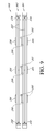
- This connector is a high speed (electrical speeds in the 2-3 GHz range) interface using a leaf spring style contact which creates a line of surface electrical conduction where the spring side of the connector touches the circuit side of the DIMM via a gold plated pad on the circuit card. See FIG. 1 .
- the present invention is an apparatus and method for making more robust the connections between a memory module and a JEDEC style DIMM connector to satisfy the aforementioned needs, provide the previously stated objects, include the above-listed features, and achieve the already articulated advantages.
- the present invention is carried out in a “inadvertent latch rotation-less” manner in a sense that the likelihood, of an unwanted disconnection of a memory module has been greatly reduced.
- the present invention is a system comprising:
- the present invention is a method comprising the steps of:
- FIG. 1 is an exploded perspective view of a prior art latchable DIMM connector system.
- FIG. 2 is a perspective view of a retention clip of the present invention.
- FIG. 3 is a perspective view of a portion of a retention clip system of the present invention which include the retention clip of FIG. 2 together with the latchable DIMM connector and memory module of FIG. 1 in an assembled configuration.
- FIG. 4 is a perspective view of a portion of the retention clip of the present invention.
- FIG. 5 is an upside down cross-sectional view of the retention clip from FIG. 4 .
- FIG. 6 is a cross-sectional view of the present invention, with a lid contacting the retention clip from FIG. 4 .
- FIG. 7 is a cross-sectional view of an alternate embodiment of a retention clip of the present invention.
- FIG. 8 is a perspective view of the retention clip of the present invention from a different angle than FIGS. 2 and 4 .
- FIG. 9 is a bottom view of a pair of adjacent retention clips of the present invention showing relationship between bumper spaces on adjacent retention clips.
- FIG. 10 is a close up view of a portion of the retention clip of FIG. 8 .
- FIG. 11 is a side view of an attached pivoting retention clip of the present invention.
- FIG. 1 there is shown a system of the prior art, generally designated 100 , including a prior art DIMM and connector 100 including a DIMM memory module 110 and a DIMM connector 120 .
- DIMM memory module 110 has a first end 102 , a second end 104 , a first end card notch 112 which provides a location for latching, a second end card notch 114 and a memory module top edge 108 .
- the DIMM memory module 110 is inserted into DIMM connector 120 , which cause first pivoting latch 122 and second pivoting latch 124 to rotate upwardly and latch at first end card notch 112 and second end card notch 114 , respectively.
- the DIMM memory module 110 can be removed by pushing outwardly (moving away from each other) on an upper portion of first pivoting latch 122 and second pivoting latch 124 . If these upper portions are pushed away from each other simultaneously, the DIMM memory module 110 may be ejected from DIMM connector 120 into the air.
- a retention clip 200 of the present invention which comprises a retention clip first end 202 , retention clip second end 204 , a retention clip central portion 208 , which has a retention clip central portion top side 209 , a retention clip central portion bottom side 207 with a retention clip bottom side top edge receiving groove 203 therein.
- Retention clip central portion 208 has a retention clip first angled portion 212 and a retention clip second angled portion 214 , which are adjacent to retention clip first latch engaging end 222 and retention clip second latch engaging end 224 , respectively.
- Each of retention clip first angled portion 212 and retention clip second angled portion 214 has a memory module card corner receiving orifice 213 ( FIG. 4 ) therethrough.
- Retention clip first latch engaging end 222 and retention clip second latch engaging end 224 have disposed thereon retention clip first latch engaging tab 232 and retention clip second latch engaging tab 234 , respectively.
- Retention clip central portion 208 further has retention clip second face bumper spacer 205 and retention clip first face bumper spacer 206 .
- Retention clip 200 spans the longitudinal length of a standard JEDEC memory module such as DIMM memory module 110 , such that each end, retention clip first end 202 and retention clip second end 204 of the retention clip 200 , exerts through the retention clip first latch engaging end 222 and retention clip second latch engaging end 224 , respectively; an inward pressure on the insertion and extraction of each latch; first pivoting latch 122 and second pivoting latch 124 .
- the inward pressure is applied by retention clip 200 in such a way as to prevent rotation of first pivoting latch 122 and second pivoting latch 124 by exploiting the inherent tensile strength properties of the material from which it is constructed.
- Retention clip 200 Key to the function of the retention clip 200 is the ability to flex around the first pivoting latch 122 and second pivoting latch 124 during the installation process of the DIMM memory module 110 into the DIMM connector 120 , but provide adequate resistance to the inherent latch rotation during chassis deflection, which often occurs during operation of the compute platform.
- the retention clip 200 therefore must be resistant to elongation in some areas but allow for flexure in the areas necessary for rotating around the latches during installation. This is in essence a snap-fit approach to retaining the DIMM in the connector.
- Retention clip 200 has spring-like properties and can be made of any suitable material which provides for minimal stretching and compression in the longitudinal direction, but with the ability for limited flexing, bending or bowing in directions other than the longitudinal direction.
- FIG. 3 there is shown a portion of disconnection protected system which includes an installed DIMM memory module 110 , in a DIMM connector 120 with a retention clip 200 . More specifically there is shown; the first pivoting latch 122 disposed in a latched orientation with the retention clip first latch engaging end 222 portion of the retention clip 200 applying a biasing force on the first pivoting latch 122 , which tends to keep the DIMM memory module 110 fully installed. Not visible in this Figure is retention clip first latch engaging tab 232 , which is present but concealing inside a slot in first pivoting latch 122 .
- a feature of the clip is the shape of the retention clip first latch engaging end 222 and retention clip second latch engaging end 224 , which interface with first pivoting latch 122 and second pivoting latch 124 .
- the angle of the retention clip 200 is designed to match that of the first pivoting latch 122 and second pivoting latch 124 such that a large force is required to allow rotation either latch.
- FIG. 4 there is shown an additional view of the retention clip 200 . More visible in FIG. 4 is retention clip bottom side top edge receiving groove 203 , which is configured to receive thereon a memory module top edge 108 . Memory module card corner receiving orifices 213 are clearly shown in retention clip first angled portion 212 and retention clip second angled portion 214 .
- FIG. 5 there is shown an upside down cross-sectional view of the retention clip 200 of FIG. 4 taken along retention clip central portion 208 at a point without a retention clip first face bumper spacer 206 of retention clip second face bumper spacer 205 .
- the diagonally hatched portion represents the material of retention clip central portion 208 which would be “cut” to allow this view to exist.
- a preferred embodiment of the retention clip 200 uses a “C” channel construction along an edge of the retention clip 200 to restrain motion of the DIMM memory module 110 in a lateral direction when installed in DIMM connector 120 .
- FIG. 6 there is shown side view of a first one of, and only shown one of, a parallel array of disconnection protected systems of the present invention in their intended environment including retention clip 200 .
- Edge of lid 602 is shown disposed over the first one but extends of all of the series of parallel systems each of which includes a retention clip 200 , DIMM memory module 110 and DIMM connector 120 such that the lid 602 contacts and applies a pressure on retention clip central portion top side 209 for each of this series of retention clips 200 .
- First pivoting latch 122 and second pivoting latch 124 are shown in a latched configuration with the retention clip 200 applying inward force therein which resists disconnection inducing rotation of the first pivoting latch 122 and second pivoting latch 124 .
- the retention clip 200 would also contain a feature which created contact with some removable chassis structure to prevent motion of a rotational nature.
- this structure is the lid 602 or cover of the chassis. Having this structural interference with the retention clip 200 prevents rotation of first pivoting latch 122 and second pivoting latch 124 and insures connectivity of the memory circuits, however this interference is not required to make the innovation useful.
- a similar example of this feature is a simple curvature of the retention clip central portion 208 such that the lid applies force to the retention clip first latch engaging end 222 and retention clip second latch engaging end 224 . Since the material has some spring characteristics, the contact with the lid 602 creates a force on the ends of first pivoting latch 122 and second pivoting latch 124 , which further secures the DIMM memory module 110 into the DIMM connector 120 .
- FIG. 7 there is shown an alternate version of the present invention which includes buttressed retention clip 700 , which is similar in many respects to retention clip 200 and which also includes first end lid contacting buttress 702 and second end lid contacting buttress 704 which can transmit force from the lid 602 to the first pivoting latch 122 and second pivoting latch 124 to provide additional biasing forces to prevent inadvertent rotation of the first pivoting latch 122 and second pivoting latch 124 . Additionally, a feature of the buttressed retention clip 700 is to capture the memory module top edge 108 near the jes 602 to resist lateral motion of the DIMM memory module 110 either through the resistance of the buttressed retention clip 700 to deflect laterally or by pressure applied by the lid 602 .
- FIG. 8 there is an alternate view of the retention clip 200 , but from a more downwardly looking viewpoint.
- FIG. 9 there is shown an upwardly looking view, of a parallel array of retention clips 200 which shows retention clip bottom side top edge receiving groove 203 and it also shows how a retention clip second face bumper spacer 205 of first parallel retention clip 992 contacts a retention clip first face bumper spacer 206 of second parallel retention clip 994 , which helps to prevent lateral motion of the DIMM memory module 110 .
- An additional feature of the retention clip 200 or buttressed retention clip 700 is to provide a self-aligning feature that allows for proper lateral spacing of the clips.
- This feature would be in the form of tapered retention clip second face bumper spacers 205 and retention clip first face bumper spacer 206 in the most obvious example, which guided one clip which was adjacent to another clip, such that alignment of second clip was optimum for installation on the second DIMM memory module.
- FIG. 10 there is shown a close up view of the retention clip first end 202 , which includes retention clip first latch engaging tab 232 which is on an interior side of retention clip first latch engaging end 222 and is designed to fit into a slot in first pivoting latch 122 during installation.
- the slot is present as a feature for the operation of the extraction and insertion action.
- the purpose of the retention clip first latch engaging tab 232 and retention clip second latch engaging tab 234 is to further deter rotation of the latch mechanism of the DIMM connector 120 by preventing upward motion on the retention clip 200 , thereby separating it from the DIMM memory module 110 and DIMM connector 120 pair.
- FIG. 11 there is shown an alternative feature of the present invention, which includes: member for transmitting latch effecting forces 1110 with a top surface 1111 .
- Member for transmitting latch effecting forces 1110 is connected to DIMM memory module 110 via module mounting structure 1120 , which can be a rivet, peg or other structure which may or may not permit rotation of the member for transmitting latch effecting forces 1110 thereabouts.
- Latch engaging structure 1130 is similar in design and function to retention clip second latch engaging end 224 .
- An additional advantage of this feature of the invention is to attach the retention clips directly to the memory modules using the JEDEC specified standard hole pattern on the module to fix the clip directly to the module using a pin or a rivet type of fastener, thereby eliminating loose pieces in the system.
Landscapes
- Details Of Connecting Devices For Male And Female Coupling (AREA)
Abstract
Description
-
- A system for reducing inadvertent disconnection of memory modules during operation in harsh environments comprising:
- a plurality of disconnection protected systems arranged in a parallel array; wherein each of said plurality of disconnection protected systems comprises:
- a
DIMM connector 120; - a
DIMM memory module 110, having a memory moduletop edge 108; - a
retention clip 200 having:- a retention clip
central portion 208, having a retention clipfirst end 202 and retention clip second end 204; - a retention clip first angled
portion 212 and retention clip secondangled portion 214 disposed on opposing ends of said retention clipcentral portion 208; - a retention clip first
latch engaging end 222 and a retention clip second latch engaging end 224 disposed on said retention clip first angledportion 212 and retention clip secondangled portion 214, respectively; - said retention clip
central portion 208 having a retention clip central portiontop side 209 and a retention clip centralportion bottom side 207, which has a retention clip bottom side topedge receiving groove 203 disposed therein, which is configured to receive therein said memory moduletop edge 108; - a plurality of retention clip first
face bumper spacers 206; - a plurality of retention clip second
face bumper spacers 205; - a retention clip first
latch engaging tab 232 disposed on an interior side of said retention clip firstlatch engaging end 222; - a retention clip second
latch engaging tab 234 disposed on an interior side said retention clip second latch engaging end 224 facing said retention clip firstlatch engaging tab 232; and - wherein said array is spatially configured such that each
retention clip 200 in said plurality of disconnection protected systems has at least one of said plurality of retention clip firstface bumper spacers 206 and said plurality of retention clip secondface bumper spacers 205 thereon in contact with one of said plurality of retention clip firstface bumper spacers 206 and said plurality of retention clip secondface bumper spacers 205 of anotherretention clip 200 of said plurality of disconnection protection systems.
- a retention clip
- a
- a plurality of disconnection protected systems arranged in a parallel array; wherein each of said plurality of disconnection protected systems comprises:
- A system for reducing inadvertent disconnection of memory modules during operation in harsh environments comprising:
-
- A method of reducing inadvertent disconnection of memory modules during operation in harsh environments comprising the steps of:
- providing a retention clip configured with a retention clip first
latch engaging end 222 and a retention clip second latch engaging end 224:- installing a
DIMM memory module 110 into aDIMM connector 120 having afirst pivoting latch 122 and asecond pivoting latch 124; and - engaging said retention clip with all of said DIMM
memory module 110; and engaging said retention clip firstlatch engaging end 222 and said retention clip second latch engaging end 224 with said first pivotinglatch 122 and saidsecond pivoting latch 124, respectively.
- installing a
- providing a retention clip configured with a retention clip first
- A method of reducing inadvertent disconnection of memory modules during operation in harsh environments comprising the steps of:
Claims (15)
Priority Applications (1)
| Application Number | Priority Date | Filing Date | Title |
|---|---|---|---|
| US15/692,289 US10193248B2 (en) | 2016-08-31 | 2017-08-31 | System and method for retaining memory modules |
Applications Claiming Priority (2)
| Application Number | Priority Date | Filing Date | Title |
|---|---|---|---|
| US201662381939P | 2016-08-31 | 2016-08-31 | |
| US15/692,289 US10193248B2 (en) | 2016-08-31 | 2017-08-31 | System and method for retaining memory modules |
Publications (2)
| Publication Number | Publication Date |
|---|---|
| US20180062287A1 US20180062287A1 (en) | 2018-03-01 |
| US10193248B2 true US10193248B2 (en) | 2019-01-29 |
Family
ID=61243672
Family Applications (1)
| Application Number | Title | Priority Date | Filing Date |
|---|---|---|---|
| US15/692,289 Active US10193248B2 (en) | 2016-08-31 | 2017-08-31 | System and method for retaining memory modules |
Country Status (1)
| Country | Link |
|---|---|
| US (1) | US10193248B2 (en) |
Cited By (2)
| Publication number | Priority date | Publication date | Assignee | Title |
|---|---|---|---|---|
| US11239607B2 (en) * | 2019-10-30 | 2022-02-01 | Innodisk Corporation | Fastening device for expansion cards |
| US11381011B2 (en) * | 2019-12-11 | 2022-07-05 | Foxconn (Kunshan) Computer Connector Co., Ltd. | Card edge connector with reinforced rotatable ejector at one end |
Families Citing this family (19)
| Publication number | Priority date | Publication date | Assignee | Title |
|---|---|---|---|---|
| US10193248B2 (en) * | 2016-08-31 | 2019-01-29 | Crystal Group, Inc. | System and method for retaining memory modules |
| US10211572B1 (en) * | 2018-04-20 | 2019-02-19 | Hewlett Packard Enterprise Development Lp | Printed circuit board retention bands |
| US10734756B2 (en) | 2018-08-10 | 2020-08-04 | Crystal Group Inc. | DIMM/expansion card retention method for highly kinematic environments |
| US10720722B2 (en) * | 2018-09-14 | 2020-07-21 | Quanta Computer Inc. | Electronics connector for facilitating treatment |
| US10888010B2 (en) * | 2019-05-24 | 2021-01-05 | Intel Corporation | Retention of dual in-line memory modules |
| US11129307B2 (en) | 2019-07-19 | 2021-09-21 | Dell Products L.P. | System and method for managing thermal states of devices |
| US11644425B2 (en) | 2019-07-19 | 2023-05-09 | Dell Products L.P. | System and method for optical state determination |
| US11234347B2 (en) * | 2019-07-19 | 2022-01-25 | Dell Products L.P. | System and method for physical management of devices |
| US11132038B2 (en) | 2019-07-19 | 2021-09-28 | Dell Products L.P. | System and method for thermal management of shadowed devices |
| US11143682B2 (en) | 2019-07-19 | 2021-10-12 | Dell Products L.P. | System and method for communicating externally from an electromagnetic interference suppressed volume |
| US11399450B2 (en) | 2019-07-19 | 2022-07-26 | Dell Products L.P. | System and method for managing electromagnetic interference |
| US10980159B2 (en) | 2019-07-19 | 2021-04-13 | Dell Products L.P. | System and method for managing multiple connections |
| US10917996B1 (en) | 2019-07-19 | 2021-02-09 | Dell Products L.P. | System and method for device level thermal management and electromagnetic interference management |
| US11378608B2 (en) | 2019-07-19 | 2022-07-05 | Dell Products L.P. | System and method for device state determination |
| US11122718B2 (en) | 2019-07-19 | 2021-09-14 | Dell Products L.P. | System and method for device level electromagnetic interference management |
| US11147194B2 (en) | 2019-08-21 | 2021-10-12 | Dell Products L.P. | System and method for managing electromagnetic interference |
| US11234350B2 (en) | 2019-08-21 | 2022-01-25 | Dell Products L.P. | System and method for isolated device access |
| CN110989783B (en) * | 2019-10-30 | 2023-08-11 | 宜鼎国际股份有限公司 | Interface card and memory card fixing device |
| US20210312953A1 (en) * | 2021-06-18 | 2021-10-07 | Intel Corporation | Dimm socket with seating floor to meet both longer length edge contacts and shorter length edge contacts |
Citations (85)
| Publication number | Priority date | Publication date | Assignee | Title |
|---|---|---|---|---|
| US3150906A (en) * | 1961-06-12 | 1964-09-29 | Commissariat Energie Atomique | Supporting frame for circuit plate |
| US3360689A (en) * | 1965-11-26 | 1967-12-26 | Bell Telephone Labor Inc | Modular plug-in component with improved support element |
| US5074800A (en) * | 1989-12-04 | 1991-12-24 | Molex Incorporated | Locking type ejection lever for use in a card edge connector |
| US5419712A (en) * | 1992-03-06 | 1995-05-30 | Augat Inc. | Edge card interconnection system |
| US5443394A (en) * | 1994-05-04 | 1995-08-22 | The Whitaker Corporation | Card edge connector having positive lock and extractor |
| US5603625A (en) * | 1993-08-16 | 1997-02-18 | Robinson Nugent, Inc. | Electrical connector socket with daughtercard ejector |
| US6007357A (en) * | 1995-05-26 | 1999-12-28 | Rambus Inc. | Chip socket assembly and chip file assembly for semiconductor chips |
| US6030251A (en) * | 1998-02-17 | 2000-02-29 | Intel Corporation | Keyed interlock and mechanical alignment integrated mechanical retention features for PC system |
| US6045385A (en) * | 1998-04-24 | 2000-04-04 | The Whitaker Corporation | Retention guides for processor module |
| US6394831B1 (en) * | 1999-08-06 | 2002-05-28 | The Whitaker Corporation | Retention member for card edge connector |
| US6517369B1 (en) * | 2002-03-14 | 2003-02-11 | International Business Machines Corporation | Retention bracket/collar for circuit cards |
| US6545877B1 (en) * | 1998-10-27 | 2003-04-08 | Dell U.S.A., L.P. | Card retaining module for expansion slots |
| US20030090879A1 (en) | 2001-06-14 | 2003-05-15 | Doblar Drew G. | Dual inline memory module |
| US6611058B2 (en) * | 1998-03-30 | 2003-08-26 | Micron Technology, Inc. | Vertical surface mount assembly and methods |
| US6767230B2 (en) * | 2002-12-17 | 2004-07-27 | Giga-Byte Technology Co., Ltd. | Card connector device having daughter board retainer |
| US20060055017A1 (en) | 2004-09-10 | 2006-03-16 | Jeong-Hyeon Cho | Stacked board-on-chip package having mirroring structure and dual inline memory module on which the stacked board-on-chip package are mounted |
| US20060129712A1 (en) | 2004-12-10 | 2006-06-15 | Siva Raghuram | Buffer chip for a multi-rank dual inline memory module (DIMM) |
| US20060129755A1 (en) | 2004-12-10 | 2006-06-15 | Siva Raghuram | Memory rank decoder for a Multi-Rank Dual Inline Memory Module (DIMM) |
| US20060126369A1 (en) | 2004-12-10 | 2006-06-15 | Siva Raghuram | Stacked DRAM memory chip for a dual inline memory module (DIMM) |
| US20070118692A1 (en) | 2005-11-23 | 2007-05-24 | Ming-Che Yu | Computer system and method for selectively supporting at least one registered dual inline memory module or at least one unbuffered dual inline memory module |
| US20070136523A1 (en) | 2005-12-08 | 2007-06-14 | Bonella Randy M | Advanced dynamic disk memory module special operations |
| US20070161275A1 (en) | 2006-01-06 | 2007-07-12 | Mcbroom Daniel L | Method and apparatus for linear insertion and removal of a memory module in a computer system |
| US20070189098A1 (en) | 2006-02-14 | 2007-08-16 | Jeff Hsieh | Memory module with independently adjustable power supply |
| US20070283054A1 (en) | 1997-12-17 | 2007-12-06 | Src Computers, Inc. | Switch/network adapter port incorporating shared memory resources selectively accessible by a direct execution logic element and one or more dense logic devices in a fully buffered dual in-line memory module format (fb-dimm) |
| US20070287333A1 (en) | 2006-06-07 | 2007-12-13 | International Business Machines Corporation | Crosstalk reduction in dual inline memory module (dimm) connectors |
| US20080007921A1 (en) | 2004-04-09 | 2008-01-10 | Pauley Robert S | High density memory module using stacked printed circuit boards |
| US20080068900A1 (en) | 2004-03-05 | 2008-03-20 | Bhakta Jayesh R | Memory module decoder |
| US7371097B1 (en) * | 2007-02-07 | 2008-05-13 | Tyco Electronics Corporation | Socket connector with latch locking member |
| US20080140952A1 (en) | 2003-06-19 | 2008-06-12 | Micro Technology, Inc. | Reconfigurable memory module and method |
| US20080155211A1 (en) | 2006-10-02 | 2008-06-26 | Novell, Inc. | System and method of imaging a memory module while in functional operation |
| US20080180899A1 (en) | 2007-01-31 | 2008-07-31 | Pearson Roger A | Methods and systems for a multi-memory module |
| US20090034327A1 (en) | 2007-07-31 | 2009-02-05 | Samsung Electronics Co., Ltd. | Thermal-emitting memory module, thermal-emitting module socket, and computer system |
| US20090119451A1 (en) | 2007-11-07 | 2009-05-07 | Christopher Haywood | Redriven/Retimed Registered Dual Inline Memory Module |
| US20090180260A1 (en) | 2008-01-10 | 2009-07-16 | Qimonda Ag | Memory module, method for manufacturing a memory module and computer system |
| US20090201711A1 (en) | 2004-03-05 | 2009-08-13 | Netlist, Inc. | Memory module with a circuit providing load isolation and memory domain translation |
| US20090217102A1 (en) | 2008-02-25 | 2009-08-27 | Kingston Technology Corp. | Fault Diagnosis of Serially-Addressed Memory Chips on a Test Adaptor Board To a Middle Memory-Module Slot on a PC Motherboard |
| US20090211083A1 (en) | 2008-02-25 | 2009-08-27 | International Business Machines Corporation | Method and Assembly For Extracting And Installing Dual In-Line Memory Module Cardlets |
| US7637748B2 (en) * | 2007-10-22 | 2009-12-29 | Asustek Computer Inc. | Electronic device and connector and card insertion method thereof |
| US20100008034A1 (en) | 2008-07-14 | 2010-01-14 | International Business Machines Corporation | Tubular memory module |
| US20100042778A1 (en) | 2008-08-18 | 2010-02-18 | Advanced Micro Devices, Inc. | Memory System Such as a Dual-Inline Memory Module (DIMm) and Computer System Using the Memory System |
| US20110016268A1 (en) | 2009-07-16 | 2011-01-20 | Shekoufeh Qawami | Phase change memory in a dual inline memory module |
| US7922506B1 (en) * | 2009-12-31 | 2011-04-12 | Hon Hai Precision Ind. Co., Ltd. | Card edge connector |
| US20110085406A1 (en) | 2004-03-05 | 2011-04-14 | Netlist, Inc. | Circuit providing load isolation and memory domain translation for memory module |
| US20110099317A1 (en) | 2008-09-08 | 2011-04-28 | Cisco Technology, Inc. | Input-output module for operation in memory module socket and method for extending a memory interface for input-output operations |
| US7955100B2 (en) * | 2009-07-01 | 2011-06-07 | Asustek Computer Inc. | Connector and electronic device having the same |
| US20110286179A1 (en) | 2010-05-24 | 2011-11-24 | International Business Machines Corporation | Memory module connector having memory module cooling structures |
| US20110286175A1 (en) | 2010-05-24 | 2011-11-24 | International Business Machines Corporation | Liquid coolant conduit secured in an unused socket for memory module cooling |
| US8075330B1 (en) * | 2011-01-28 | 2011-12-13 | Hong Fu Jin Precision Industry (Shenzhen) Co., Ltd. | Mounting apparatus for memory card |
| US8113863B2 (en) * | 2009-08-25 | 2012-02-14 | Tyco Electronics Corporation | Socket connector having a thermally conductive insert |
| US20120151287A1 (en) | 2010-12-10 | 2012-06-14 | Kingston Technology Corp. | Memory-Module Extender Card for Visually Decoding Addresses from Diagnostic Programs and Ignoring Operating System Accesses |
| US20120271990A1 (en) | 2007-06-01 | 2012-10-25 | Netlist, Inc. | Non-Volatile Memory Module |
| US20130007356A1 (en) | 2011-06-30 | 2013-01-03 | International Business Machines Corporation | Assigning A Classification To A Dual In-line Memory Module (DIMM) |
| US20130019048A1 (en) | 2011-07-15 | 2013-01-17 | International Business Machines Corporation | Memory Access To A Dual In-line Memory Module Form Factor Flash Memory |
| US20130070410A1 (en) | 2011-09-16 | 2013-03-21 | Hon Hai Precision Industry Co., Ltd. | Serial advanced technology attachment dual in-line memory module and computer system |
| US8403689B2 (en) * | 2010-12-25 | 2013-03-26 | Hon Hai Precision Ind. Co., Ltd | Card edge connector |
| US20130074339A1 (en) | 2011-09-28 | 2013-03-28 | International Business Machines Corporation | Overmolded Dual In-Line Memory Module Cooling Structure |
| US20130114200A1 (en) | 2011-11-08 | 2013-05-09 | Hon Hai Precision Industry Co., Ltd. | Computer system having data transfer rate indication function of serial advanced technology attachment dual in-line memory module |
| US20130135812A1 (en) | 2011-11-28 | 2013-05-30 | International Business Machines Corporation | Liquid-cooling memory modules with liquid flow pipes between memory module sockets |
| US8559187B2 (en) * | 2011-04-28 | 2013-10-15 | Hong Fu Jin Precision Industry (Shenzhen) Co., Ltd. | Mounting apparatus for expansion card |
| US20130290589A1 (en) | 2012-04-25 | 2013-10-31 | Hon Hai Precision Industry Co., Ltd. | Test circuit for memory module |
| US8665587B2 (en) * | 2011-04-29 | 2014-03-04 | Hong Fu Jin Precision Industry (Shenzhen) Co., Ltd | Mounting apparatus for expansion card |
| US20140185227A1 (en) | 2012-12-29 | 2014-07-03 | Hon Hai Precision Industry Co., Ltd. | Computer system having capacity indication function of serial advanced technology attachment dual in-line memory module device |
| US8771001B2 (en) * | 2011-08-11 | 2014-07-08 | Hon Hai Precision Industry Co., Ltd. | Card edge connector |
| US20140211404A1 (en) | 2013-01-30 | 2014-07-31 | Adata Technology Co., Ltd. | Detachable assembly and memory module using the same |
| US20140241062A1 (en) | 2013-02-27 | 2014-08-28 | Lsi Corporation | Modular, Scalable Rigid Flex Memory Module |
| US20150004824A1 (en) * | 2013-06-28 | 2015-01-01 | Hewlett-Packard Development Company, L.P. | Dual Inline Memory Module Socket |
| US20150089279A1 (en) | 2013-09-24 | 2015-03-26 | International Business Machines Corporation | Implementing memory module communications with a host processor in multiported memory configurations |
| US20150127890A1 (en) | 2012-06-28 | 2015-05-07 | Hewlett-Packard Development Company, L.P. | Memory module with a dual-port buffer |
| US9060453B2 (en) * | 2013-02-20 | 2015-06-16 | Lenovo Enterprise Solutions (Singapore) Pte. Ltd. | Frame having attachment arms, a latching mechanism and handling levers |
| US20150169238A1 (en) | 2011-07-28 | 2015-06-18 | Netlist, Inc. | Hybrid memory module and system and method of operating the same |
| US9173310B2 (en) * | 2012-08-09 | 2015-10-27 | Lenovo Enterprise Solutions (Singapore) Pte. Ltd. | Latch for securing a compute node in a component storage rack |
| US9172164B2 (en) * | 2013-06-20 | 2015-10-27 | Hon Hai Precision Industry Co., Ltd. | Card edge connector with an improved housing |
| US20150363107A1 (en) | 2014-06-17 | 2015-12-17 | Rambus Inc. | Memory module and system supporting parallel and serial access modes |
| US20160011802A1 (en) | 2014-07-09 | 2016-01-14 | Dell Products, Lp | System and Method for Enabling Transportability of a Non Volatile Dual Inline Memory Module |
| US9240639B2 (en) * | 2013-06-08 | 2016-01-19 | Hon Hai Precision Industry Co., Ltd. | Card edge connector with a lock mechanism |
| US20160019138A1 (en) | 2011-07-28 | 2016-01-21 | Netlist, Inc. | Memory module and system and method of operation |
| US9252528B2 (en) * | 2013-07-02 | 2016-02-02 | Germane Systems, Llc | Printed circuit board, method of manufacturing same, and method of mounting the circuit board in a connector socket |
| US20160071610A1 (en) | 2014-09-05 | 2016-03-10 | Winbond Electronics Corp. | Flash memory, memory module, computer-readable recording medium and operating method |
| US20160070616A1 (en) | 2013-07-31 | 2016-03-10 | Hewlett-Packard Development Company, L.P. | Off-memory-module ecc-supplemental memory system |
| US20160081217A1 (en) | 2013-06-18 | 2016-03-17 | Hewlett-Packard Development Company, L.P. | Confirm proper seating of a dual inline memory module |
| US20160085670A1 (en) | 2013-05-30 | 2016-03-24 | Huawei Technologies Co., Ltd. | Memory Access Method, Buffer Scheduler and Memory Module |
| US9329643B2 (en) * | 2013-06-17 | 2016-05-03 | Michael R. Tobias | Apparatus for holding a semiconductor module |
| US20160196073A1 (en) | 2013-09-16 | 2016-07-07 | Huawei Technologies Co., Ltd. | Memory Module Access Method and Apparatus |
| US20160270249A1 (en) * | 2013-11-15 | 2016-09-15 | Hewlett-Packard Development Company, L.P. | Memory module latches and ejectors |
| US20180062287A1 (en) * | 2016-08-31 | 2018-03-01 | Crystal Group Inc. | System and method for retaining memory modules |
-
2017
- 2017-08-31 US US15/692,289 patent/US10193248B2/en active Active
Patent Citations (99)
| Publication number | Priority date | Publication date | Assignee | Title |
|---|---|---|---|---|
| US3150906A (en) * | 1961-06-12 | 1964-09-29 | Commissariat Energie Atomique | Supporting frame for circuit plate |
| US3360689A (en) * | 1965-11-26 | 1967-12-26 | Bell Telephone Labor Inc | Modular plug-in component with improved support element |
| US5074800A (en) * | 1989-12-04 | 1991-12-24 | Molex Incorporated | Locking type ejection lever for use in a card edge connector |
| US5419712A (en) * | 1992-03-06 | 1995-05-30 | Augat Inc. | Edge card interconnection system |
| US5603625A (en) * | 1993-08-16 | 1997-02-18 | Robinson Nugent, Inc. | Electrical connector socket with daughtercard ejector |
| US5443394A (en) * | 1994-05-04 | 1995-08-22 | The Whitaker Corporation | Card edge connector having positive lock and extractor |
| US6007357A (en) * | 1995-05-26 | 1999-12-28 | Rambus Inc. | Chip socket assembly and chip file assembly for semiconductor chips |
| US6589059B2 (en) * | 1995-05-26 | 2003-07-08 | Rambus, Inc. | Chip socket assembly and chip file assembly for semiconductor chips |
| US20070283054A1 (en) | 1997-12-17 | 2007-12-06 | Src Computers, Inc. | Switch/network adapter port incorporating shared memory resources selectively accessible by a direct execution logic element and one or more dense logic devices in a fully buffered dual in-line memory module format (fb-dimm) |
| US6030251A (en) * | 1998-02-17 | 2000-02-29 | Intel Corporation | Keyed interlock and mechanical alignment integrated mechanical retention features for PC system |
| US6611058B2 (en) * | 1998-03-30 | 2003-08-26 | Micron Technology, Inc. | Vertical surface mount assembly and methods |
| US6045385A (en) * | 1998-04-24 | 2000-04-04 | The Whitaker Corporation | Retention guides for processor module |
| US6545877B1 (en) * | 1998-10-27 | 2003-04-08 | Dell U.S.A., L.P. | Card retaining module for expansion slots |
| US6394831B1 (en) * | 1999-08-06 | 2002-05-28 | The Whitaker Corporation | Retention member for card edge connector |
| US20030090879A1 (en) | 2001-06-14 | 2003-05-15 | Doblar Drew G. | Dual inline memory module |
| US6517369B1 (en) * | 2002-03-14 | 2003-02-11 | International Business Machines Corporation | Retention bracket/collar for circuit cards |
| US6767230B2 (en) * | 2002-12-17 | 2004-07-27 | Giga-Byte Technology Co., Ltd. | Card connector device having daughter board retainer |
| US20110029746A1 (en) | 2003-06-19 | 2011-02-03 | Round Rock Research, Llc | Reconfigurable memory module and method |
| US20110246743A1 (en) | 2003-06-19 | 2011-10-06 | Round Rock Research, Llc | Reconfigurable memory module and method |
| US20080140952A1 (en) | 2003-06-19 | 2008-06-12 | Micro Technology, Inc. | Reconfigurable memory module and method |
| US20120278524A1 (en) | 2003-06-19 | 2012-11-01 | Round Rock Research, Llc | Reconfigurable memory module and method |
| US20080068900A1 (en) | 2004-03-05 | 2008-03-20 | Bhakta Jayesh R | Memory module decoder |
| US20110090749A1 (en) | 2004-03-05 | 2011-04-21 | Netlist, Inc. | Circuit for providing chip-select signals to a plurality of ranks of a ddr memory module |
| US20100091540A1 (en) | 2004-03-05 | 2010-04-15 | Netlist, Inc. | Memory module decoder |
| US20100128507A1 (en) | 2004-03-05 | 2010-05-27 | Netlist, Inc. | Circuit providing load isolation and memory domain translation for memory module |
| US20140040569A1 (en) | 2004-03-05 | 2014-02-06 | Netlist, Inc. | Load-reducing circuit for memory module |
| US20110085406A1 (en) | 2004-03-05 | 2011-04-14 | Netlist, Inc. | Circuit providing load isolation and memory domain translation for memory module |
| US20090201711A1 (en) | 2004-03-05 | 2009-08-13 | Netlist, Inc. | Memory module with a circuit providing load isolation and memory domain translation |
| US20080007921A1 (en) | 2004-04-09 | 2008-01-10 | Pauley Robert S | High density memory module using stacked printed circuit boards |
| US20060055017A1 (en) | 2004-09-10 | 2006-03-16 | Jeong-Hyeon Cho | Stacked board-on-chip package having mirroring structure and dual inline memory module on which the stacked board-on-chip package are mounted |
| US20060126369A1 (en) | 2004-12-10 | 2006-06-15 | Siva Raghuram | Stacked DRAM memory chip for a dual inline memory module (DIMM) |
| US20060129755A1 (en) | 2004-12-10 | 2006-06-15 | Siva Raghuram | Memory rank decoder for a Multi-Rank Dual Inline Memory Module (DIMM) |
| US20060129712A1 (en) | 2004-12-10 | 2006-06-15 | Siva Raghuram | Buffer chip for a multi-rank dual inline memory module (DIMM) |
| US20070118692A1 (en) | 2005-11-23 | 2007-05-24 | Ming-Che Yu | Computer system and method for selectively supporting at least one registered dual inline memory module or at least one unbuffered dual inline memory module |
| US20070136523A1 (en) | 2005-12-08 | 2007-06-14 | Bonella Randy M | Advanced dynamic disk memory module special operations |
| US20070161275A1 (en) | 2006-01-06 | 2007-07-12 | Mcbroom Daniel L | Method and apparatus for linear insertion and removal of a memory module in a computer system |
| US20070189098A1 (en) | 2006-02-14 | 2007-08-16 | Jeff Hsieh | Memory module with independently adjustable power supply |
| US20070287333A1 (en) | 2006-06-07 | 2007-12-13 | International Business Machines Corporation | Crosstalk reduction in dual inline memory module (dimm) connectors |
| US20080207059A1 (en) | 2006-06-07 | 2008-08-28 | International Business Machines Corporation | Crosstalk reduction in dual inline memory module (dimm) connectors |
| US20080155211A1 (en) | 2006-10-02 | 2008-06-26 | Novell, Inc. | System and method of imaging a memory module while in functional operation |
| US20100191904A1 (en) | 2006-10-02 | 2010-07-29 | Novell, Inc. | System and method of imaging a memory module while in functional operation |
| US20080180899A1 (en) | 2007-01-31 | 2008-07-31 | Pearson Roger A | Methods and systems for a multi-memory module |
| US7371097B1 (en) * | 2007-02-07 | 2008-05-13 | Tyco Electronics Corporation | Socket connector with latch locking member |
| US20120271990A1 (en) | 2007-06-01 | 2012-10-25 | Netlist, Inc. | Non-Volatile Memory Module |
| US20090034327A1 (en) | 2007-07-31 | 2009-02-05 | Samsung Electronics Co., Ltd. | Thermal-emitting memory module, thermal-emitting module socket, and computer system |
| US7637748B2 (en) * | 2007-10-22 | 2009-12-29 | Asustek Computer Inc. | Electronic device and connector and card insertion method thereof |
| US20090119451A1 (en) | 2007-11-07 | 2009-05-07 | Christopher Haywood | Redriven/Retimed Registered Dual Inline Memory Module |
| US20090180260A1 (en) | 2008-01-10 | 2009-07-16 | Qimonda Ag | Memory module, method for manufacturing a memory module and computer system |
| US20090217102A1 (en) | 2008-02-25 | 2009-08-27 | Kingston Technology Corp. | Fault Diagnosis of Serially-Addressed Memory Chips on a Test Adaptor Board To a Middle Memory-Module Slot on a PC Motherboard |
| US20090211083A1 (en) | 2008-02-25 | 2009-08-27 | International Business Machines Corporation | Method and Assembly For Extracting And Installing Dual In-Line Memory Module Cardlets |
| US20100008034A1 (en) | 2008-07-14 | 2010-01-14 | International Business Machines Corporation | Tubular memory module |
| US20100042778A1 (en) | 2008-08-18 | 2010-02-18 | Advanced Micro Devices, Inc. | Memory System Such as a Dual-Inline Memory Module (DIMm) and Computer System Using the Memory System |
| US20110099317A1 (en) | 2008-09-08 | 2011-04-28 | Cisco Technology, Inc. | Input-output module for operation in memory module socket and method for extending a memory interface for input-output operations |
| US7955100B2 (en) * | 2009-07-01 | 2011-06-07 | Asustek Computer Inc. | Connector and electronic device having the same |
| US20140095781A1 (en) | 2009-07-16 | 2014-04-03 | Micron Technology, Inc. | Phase change memory in a dual inline memory module |
| US20110016268A1 (en) | 2009-07-16 | 2011-01-20 | Shekoufeh Qawami | Phase change memory in a dual inline memory module |
| US8113863B2 (en) * | 2009-08-25 | 2012-02-14 | Tyco Electronics Corporation | Socket connector having a thermally conductive insert |
| US7922506B1 (en) * | 2009-12-31 | 2011-04-12 | Hon Hai Precision Ind. Co., Ltd. | Card edge connector |
| US20110286175A1 (en) | 2010-05-24 | 2011-11-24 | International Business Machines Corporation | Liquid coolant conduit secured in an unused socket for memory module cooling |
| US20110286179A1 (en) | 2010-05-24 | 2011-11-24 | International Business Machines Corporation | Memory module connector having memory module cooling structures |
| US20120151287A1 (en) | 2010-12-10 | 2012-06-14 | Kingston Technology Corp. | Memory-Module Extender Card for Visually Decoding Addresses from Diagnostic Programs and Ignoring Operating System Accesses |
| US20130151904A1 (en) | 2010-12-10 | 2013-06-13 | Kingston Technology Corp. | Memory-Module Extender Card for Visually Decoding Addresses from Diagnostic Programs and Ignoring Operating System Accesses |
| US8403689B2 (en) * | 2010-12-25 | 2013-03-26 | Hon Hai Precision Ind. Co., Ltd | Card edge connector |
| US8075330B1 (en) * | 2011-01-28 | 2011-12-13 | Hong Fu Jin Precision Industry (Shenzhen) Co., Ltd. | Mounting apparatus for memory card |
| US8559187B2 (en) * | 2011-04-28 | 2013-10-15 | Hong Fu Jin Precision Industry (Shenzhen) Co., Ltd. | Mounting apparatus for expansion card |
| US8665587B2 (en) * | 2011-04-29 | 2014-03-04 | Hong Fu Jin Precision Industry (Shenzhen) Co., Ltd | Mounting apparatus for expansion card |
| US20130007356A1 (en) | 2011-06-30 | 2013-01-03 | International Business Machines Corporation | Assigning A Classification To A Dual In-line Memory Module (DIMM) |
| US20130019048A1 (en) | 2011-07-15 | 2013-01-17 | International Business Machines Corporation | Memory Access To A Dual In-line Memory Module Form Factor Flash Memory |
| US20160019138A1 (en) | 2011-07-28 | 2016-01-21 | Netlist, Inc. | Memory module and system and method of operation |
| US20150169238A1 (en) | 2011-07-28 | 2015-06-18 | Netlist, Inc. | Hybrid memory module and system and method of operating the same |
| US8771001B2 (en) * | 2011-08-11 | 2014-07-08 | Hon Hai Precision Industry Co., Ltd. | Card edge connector |
| US20130070410A1 (en) | 2011-09-16 | 2013-03-21 | Hon Hai Precision Industry Co., Ltd. | Serial advanced technology attachment dual in-line memory module and computer system |
| US20150033550A1 (en) | 2011-09-28 | 2015-02-05 | Lenovo (Singapore) Pte. Ltd. | Overmolded dual in-line memory module cooling structure |
| US20130074339A1 (en) | 2011-09-28 | 2013-03-28 | International Business Machines Corporation | Overmolded Dual In-Line Memory Module Cooling Structure |
| US20130114200A1 (en) | 2011-11-08 | 2013-05-09 | Hon Hai Precision Industry Co., Ltd. | Computer system having data transfer rate indication function of serial advanced technology attachment dual in-line memory module |
| US20130135812A1 (en) | 2011-11-28 | 2013-05-30 | International Business Machines Corporation | Liquid-cooling memory modules with liquid flow pipes between memory module sockets |
| US20130290589A1 (en) | 2012-04-25 | 2013-10-31 | Hon Hai Precision Industry Co., Ltd. | Test circuit for memory module |
| US20150127890A1 (en) | 2012-06-28 | 2015-05-07 | Hewlett-Packard Development Company, L.P. | Memory module with a dual-port buffer |
| US9173310B2 (en) * | 2012-08-09 | 2015-10-27 | Lenovo Enterprise Solutions (Singapore) Pte. Ltd. | Latch for securing a compute node in a component storage rack |
| US20140185227A1 (en) | 2012-12-29 | 2014-07-03 | Hon Hai Precision Industry Co., Ltd. | Computer system having capacity indication function of serial advanced technology attachment dual in-line memory module device |
| US20140211404A1 (en) | 2013-01-30 | 2014-07-31 | Adata Technology Co., Ltd. | Detachable assembly and memory module using the same |
| US9060453B2 (en) * | 2013-02-20 | 2015-06-16 | Lenovo Enterprise Solutions (Singapore) Pte. Ltd. | Frame having attachment arms, a latching mechanism and handling levers |
| US9839140B2 (en) * | 2013-02-20 | 2017-12-05 | Lenovo Enterprise Solutions (Singapore) Pte. Ltd. | Method for manufacturing an electronic component carrier for mounting the electronic component to a circuit board |
| US20140241062A1 (en) | 2013-02-27 | 2014-08-28 | Lsi Corporation | Modular, Scalable Rigid Flex Memory Module |
| US20160085670A1 (en) | 2013-05-30 | 2016-03-24 | Huawei Technologies Co., Ltd. | Memory Access Method, Buffer Scheduler and Memory Module |
| US9240639B2 (en) * | 2013-06-08 | 2016-01-19 | Hon Hai Precision Industry Co., Ltd. | Card edge connector with a lock mechanism |
| US9329643B2 (en) * | 2013-06-17 | 2016-05-03 | Michael R. Tobias | Apparatus for holding a semiconductor module |
| US20160081217A1 (en) | 2013-06-18 | 2016-03-17 | Hewlett-Packard Development Company, L.P. | Confirm proper seating of a dual inline memory module |
| US9172164B2 (en) * | 2013-06-20 | 2015-10-27 | Hon Hai Precision Industry Co., Ltd. | Card edge connector with an improved housing |
| US20150004824A1 (en) * | 2013-06-28 | 2015-01-01 | Hewlett-Packard Development Company, L.P. | Dual Inline Memory Module Socket |
| US9252528B2 (en) * | 2013-07-02 | 2016-02-02 | Germane Systems, Llc | Printed circuit board, method of manufacturing same, and method of mounting the circuit board in a connector socket |
| US20160070616A1 (en) | 2013-07-31 | 2016-03-10 | Hewlett-Packard Development Company, L.P. | Off-memory-module ecc-supplemental memory system |
| US20160196073A1 (en) | 2013-09-16 | 2016-07-07 | Huawei Technologies Co., Ltd. | Memory Module Access Method and Apparatus |
| US20150089279A1 (en) | 2013-09-24 | 2015-03-26 | International Business Machines Corporation | Implementing memory module communications with a host processor in multiported memory configurations |
| US20160270249A1 (en) * | 2013-11-15 | 2016-09-15 | Hewlett-Packard Development Company, L.P. | Memory module latches and ejectors |
| US20150363107A1 (en) | 2014-06-17 | 2015-12-17 | Rambus Inc. | Memory module and system supporting parallel and serial access modes |
| US20160011802A1 (en) | 2014-07-09 | 2016-01-14 | Dell Products, Lp | System and Method for Enabling Transportability of a Non Volatile Dual Inline Memory Module |
| US20160071610A1 (en) | 2014-09-05 | 2016-03-10 | Winbond Electronics Corp. | Flash memory, memory module, computer-readable recording medium and operating method |
| US20180062287A1 (en) * | 2016-08-31 | 2018-03-01 | Crystal Group Inc. | System and method for retaining memory modules |
Cited By (2)
| Publication number | Priority date | Publication date | Assignee | Title |
|---|---|---|---|---|
| US11239607B2 (en) * | 2019-10-30 | 2022-02-01 | Innodisk Corporation | Fastening device for expansion cards |
| US11381011B2 (en) * | 2019-12-11 | 2022-07-05 | Foxconn (Kunshan) Computer Connector Co., Ltd. | Card edge connector with reinforced rotatable ejector at one end |
Also Published As
| Publication number | Publication date |
|---|---|
| US20180062287A1 (en) | 2018-03-01 |
Similar Documents
| Publication | Publication Date | Title |
|---|---|---|
| US10193248B2 (en) | System and method for retaining memory modules | |
| US9166317B2 (en) | High-speed connector assembly | |
| US7654829B1 (en) | Electronic device and connector assembly | |
| US8837135B2 (en) | Expansion module for interface card, computer case assembly, and computer system | |
| US20090191736A1 (en) | Card edge connector with pick-up member | |
| US8570731B2 (en) | Mounting apparatus for expansion card | |
| US9640884B2 (en) | Low profile circuit connector | |
| US8625258B2 (en) | Mounting apparatus for expansion card | |
| US9054441B2 (en) | Connector | |
| US7244134B2 (en) | Electrical connector having a locking device | |
| CN102884873A (en) | Apparatus for securing electronic equipment | |
| US6210195B1 (en) | Card edge connector with card retaining means | |
| TWI455418B (en) | Card edge connector | |
| US5242312A (en) | Board to socket retainer clip | |
| US6368124B1 (en) | Card edge connector with daughter board retainer | |
| US7990733B2 (en) | Mounting apparatus for PCI card | |
| US6626685B2 (en) | Card connector cover and card connector assembly | |
| US6350154B1 (en) | Adapter for connector | |
| CN107248679B (en) | Press fixing device and electronic equipment | |
| US6179652B1 (en) | IC card connector assembly | |
| US8512063B2 (en) | Attachment mechanism for electronic component | |
| US10355408B2 (en) | Connector having latches | |
| TWI754507B (en) | Memory assembly and electronic device | |
| US8847076B2 (en) | Attachment mechanism for electronic component | |
| US9425524B1 (en) | Electrical connector mounted on a circuit board and having a retention section with a bearing section and a limiting section |
Legal Events
| Date | Code | Title | Description |
|---|---|---|---|
| FEPP | Fee payment procedure |
Free format text: ENTITY STATUS SET TO UNDISCOUNTED (ORIGINAL EVENT CODE: BIG.); ENTITY STATUS OF PATENT OWNER: LARGE ENTITY |
|
| AS | Assignment |
Owner name: CRYSTAL GROUP, INC., IOWA Free format text: ASSIGNMENT OF ASSIGNORS INTEREST;ASSIGNORS:SHAW, JAMES E;MANSON, RACHEL;MARSDEN, CHASE;AND OTHERS;SIGNING DATES FROM 20170913 TO 20170914;REEL/FRAME:043601/0459 |
|
| STCF | Information on status: patent grant |
Free format text: PATENTED CASE |
|
| MAFP | Maintenance fee payment |
Free format text: PAYMENT OF MAINTENANCE FEE, 4TH YEAR, LARGE ENTITY (ORIGINAL EVENT CODE: M1551); ENTITY STATUS OF PATENT OWNER: LARGE ENTITY Year of fee payment: 4 |