US10186675B2 - Top-emitting white organic light emitting diode device, method for manufacturing the same, and display apparatus - Google Patents
Top-emitting white organic light emitting diode device, method for manufacturing the same, and display apparatus Download PDFInfo
- Publication number
- US10186675B2 US10186675B2 US14/888,736 US201514888736A US10186675B2 US 10186675 B2 US10186675 B2 US 10186675B2 US 201514888736 A US201514888736 A US 201514888736A US 10186675 B2 US10186675 B2 US 10186675B2
- Authority
- US
- United States
- Prior art keywords
- layer
- electrode layer
- lattice structure
- bumps
- substrate
- Prior art date
- Legal status (The legal status is an assumption and is not a legal conclusion. Google has not performed a legal analysis and makes no representation as to the accuracy of the status listed.)
- Active, expires
Links
- 238000000034 method Methods 0.000 title claims abstract description 27
- 238000004519 manufacturing process Methods 0.000 title claims abstract description 11
- 239000010410 layer Substances 0.000 claims abstract description 164
- 239000012044 organic layer Substances 0.000 claims abstract description 70
- 239000000758 substrate Substances 0.000 claims abstract description 44
- 239000011347 resin Substances 0.000 claims description 62
- 229920005989 resin Polymers 0.000 claims description 62
- 239000007788 liquid Substances 0.000 claims description 16
- 239000011248 coating agent Substances 0.000 claims description 12
- 238000000576 coating method Methods 0.000 claims description 12
- 239000004642 Polyimide Substances 0.000 claims description 4
- 229920001721 polyimide Polymers 0.000 claims description 4
- 238000006116 polymerization reaction Methods 0.000 claims description 4
- 239000002243 precursor Substances 0.000 claims description 4
- 239000002904 solvent Substances 0.000 claims description 4
- 230000000694 effects Effects 0.000 description 10
- 238000000151 deposition Methods 0.000 description 6
- 238000002347 injection Methods 0.000 description 6
- 239000007924 injection Substances 0.000 description 6
- 230000008569 process Effects 0.000 description 5
- 238000005516 engineering process Methods 0.000 description 4
- 239000010408 film Substances 0.000 description 4
- 239000002346 layers by function Substances 0.000 description 4
- 239000000463 material Substances 0.000 description 4
- 230000003247 decreasing effect Effects 0.000 description 3
- 239000000956 alloy Substances 0.000 description 2
- 229910045601 alloy Inorganic materials 0.000 description 2
- 239000003086 colorant Substances 0.000 description 2
- PCHJSUWPFVWCPO-UHFFFAOYSA-N gold Chemical compound [Au] PCHJSUWPFVWCPO-UHFFFAOYSA-N 0.000 description 2
- 229910052737 gold Inorganic materials 0.000 description 2
- 239000010931 gold Substances 0.000 description 2
- 238000012986 modification Methods 0.000 description 2
- 230000004048 modification Effects 0.000 description 2
- 238000004806 packaging method and process Methods 0.000 description 2
- 238000000197 pyrolysis Methods 0.000 description 2
- 229910052709 silver Inorganic materials 0.000 description 2
- 239000004332 silver Substances 0.000 description 2
- 238000001228 spectrum Methods 0.000 description 2
- 238000004528 spin coating Methods 0.000 description 2
- 239000010409 thin film Substances 0.000 description 2
- BQCADISMDOOEFD-UHFFFAOYSA-N Silver Chemical compound [Ag] BQCADISMDOOEFD-UHFFFAOYSA-N 0.000 description 1
- 229910052782 aluminium Inorganic materials 0.000 description 1
- XAGFODPZIPBFFR-UHFFFAOYSA-N aluminium Chemical compound [Al] XAGFODPZIPBFFR-UHFFFAOYSA-N 0.000 description 1
- 230000009286 beneficial effect Effects 0.000 description 1
- 238000013461 design Methods 0.000 description 1
- 239000007772 electrode material Substances 0.000 description 1
- 238000001194 electroluminescence spectrum Methods 0.000 description 1
- 230000002708 enhancing effect Effects 0.000 description 1
- 239000011521 glass Substances 0.000 description 1
- 230000010354 integration Effects 0.000 description 1
- 229910052751 metal Inorganic materials 0.000 description 1
- 239000002184 metal Substances 0.000 description 1
- 239000007769 metal material Substances 0.000 description 1
- 238000012827 research and development Methods 0.000 description 1
- 230000004044 response Effects 0.000 description 1
- 239000000243 solution Substances 0.000 description 1
Images


Classifications
-
- H—ELECTRICITY
- H10—SEMICONDUCTOR DEVICES; ELECTRIC SOLID-STATE DEVICES NOT OTHERWISE PROVIDED FOR
- H10K—ORGANIC ELECTRIC SOLID-STATE DEVICES
- H10K50/00—Organic light-emitting devices
- H10K50/10—OLEDs or polymer light-emitting diodes [PLED]
- H10K50/11—OLEDs or polymer light-emitting diodes [PLED] characterised by the electroluminescent [EL] layers
- H10K50/125—OLEDs or polymer light-emitting diodes [PLED] characterised by the electroluminescent [EL] layers specially adapted for multicolour light emission, e.g. for emitting white light
- H10K50/13—OLEDs or polymer light-emitting diodes [PLED] characterised by the electroluminescent [EL] layers specially adapted for multicolour light emission, e.g. for emitting white light comprising stacked EL layers within one EL unit
-
- H—ELECTRICITY
- H10—SEMICONDUCTOR DEVICES; ELECTRIC SOLID-STATE DEVICES NOT OTHERWISE PROVIDED FOR
- H10K—ORGANIC ELECTRIC SOLID-STATE DEVICES
- H10K59/00—Integrated devices, or assemblies of multiple devices, comprising at least one organic light-emitting element covered by group H10K50/00
- H10K59/80—Constructional details
- H10K59/805—Electrodes
- H10K59/8051—Anodes
- H10K59/80515—Anodes characterised by their shape
-
- H01L51/504—
-
- H01L51/52—
-
- H01L51/5203—
-
- H01L51/5237—
-
- H01L51/56—
-
- H—ELECTRICITY
- H10—SEMICONDUCTOR DEVICES; ELECTRIC SOLID-STATE DEVICES NOT OTHERWISE PROVIDED FOR
- H10K—ORGANIC ELECTRIC SOLID-STATE DEVICES
- H10K50/00—Organic light-emitting devices
- H10K50/80—Constructional details
-
- H—ELECTRICITY
- H10—SEMICONDUCTOR DEVICES; ELECTRIC SOLID-STATE DEVICES NOT OTHERWISE PROVIDED FOR
- H10K—ORGANIC ELECTRIC SOLID-STATE DEVICES
- H10K50/00—Organic light-emitting devices
- H10K50/80—Constructional details
- H10K50/805—Electrodes
-
- H—ELECTRICITY
- H10—SEMICONDUCTOR DEVICES; ELECTRIC SOLID-STATE DEVICES NOT OTHERWISE PROVIDED FOR
- H10K—ORGANIC ELECTRIC SOLID-STATE DEVICES
- H10K50/00—Organic light-emitting devices
- H10K50/80—Constructional details
- H10K50/805—Electrodes
- H10K50/81—Anodes
- H10K50/813—Anodes characterised by their shape
-
- H—ELECTRICITY
- H10—SEMICONDUCTOR DEVICES; ELECTRIC SOLID-STATE DEVICES NOT OTHERWISE PROVIDED FOR
- H10K—ORGANIC ELECTRIC SOLID-STATE DEVICES
- H10K50/00—Organic light-emitting devices
- H10K50/80—Constructional details
- H10K50/805—Electrodes
- H10K50/82—Cathodes
- H10K50/822—Cathodes characterised by their shape
-
- H—ELECTRICITY
- H10—SEMICONDUCTOR DEVICES; ELECTRIC SOLID-STATE DEVICES NOT OTHERWISE PROVIDED FOR
- H10K—ORGANIC ELECTRIC SOLID-STATE DEVICES
- H10K50/00—Organic light-emitting devices
- H10K50/80—Constructional details
- H10K50/84—Passivation; Containers; Encapsulations
-
- H—ELECTRICITY
- H10—SEMICONDUCTOR DEVICES; ELECTRIC SOLID-STATE DEVICES NOT OTHERWISE PROVIDED FOR
- H10K—ORGANIC ELECTRIC SOLID-STATE DEVICES
- H10K50/00—Organic light-emitting devices
- H10K50/80—Constructional details
- H10K50/85—Arrangements for extracting light from the devices
- H10K50/852—Arrangements for extracting light from the devices comprising a resonant cavity structure, e.g. Bragg reflector pair
-
- H—ELECTRICITY
- H10—SEMICONDUCTOR DEVICES; ELECTRIC SOLID-STATE DEVICES NOT OTHERWISE PROVIDED FOR
- H10K—ORGANIC ELECTRIC SOLID-STATE DEVICES
- H10K59/00—Integrated devices, or assemblies of multiple devices, comprising at least one organic light-emitting element covered by group H10K50/00
- H10K59/80—Constructional details
- H10K59/875—Arrangements for extracting light from the devices
- H10K59/876—Arrangements for extracting light from the devices comprising a resonant cavity structure, e.g. Bragg reflector pair
-
- H—ELECTRICITY
- H10—SEMICONDUCTOR DEVICES; ELECTRIC SOLID-STATE DEVICES NOT OTHERWISE PROVIDED FOR
- H10K—ORGANIC ELECTRIC SOLID-STATE DEVICES
- H10K71/00—Manufacture or treatment specially adapted for the organic devices covered by this subclass
-
- H—ELECTRICITY
- H10—SEMICONDUCTOR DEVICES; ELECTRIC SOLID-STATE DEVICES NOT OTHERWISE PROVIDED FOR
- H10K—ORGANIC ELECTRIC SOLID-STATE DEVICES
- H10K2102/00—Constructional details relating to the organic devices covered by this subclass
- H10K2102/301—Details of OLEDs
- H10K2102/302—Details of OLEDs of OLED structures
- H10K2102/3023—Direction of light emission
- H10K2102/3026—Top emission
-
- H—ELECTRICITY
- H10—SEMICONDUCTOR DEVICES; ELECTRIC SOLID-STATE DEVICES NOT OTHERWISE PROVIDED FOR
- H10K—ORGANIC ELECTRIC SOLID-STATE DEVICES
- H10K2102/00—Constructional details relating to the organic devices covered by this subclass
- H10K2102/301—Details of OLEDs
- H10K2102/351—Thickness
Definitions
- the present disclosure relates to the field of organic light-emitting diode (OLED) display technology, and in particular to a top-emitting white OLED device, a method for manufacturing the same and a display apparatus.
- OLED organic light-emitting diode
- OLED organic light-emitting diode
- the bottom-emitting OLED refers to an OLED where light is emitted from a substrate
- the top-emitting OLED refers to an OLED where light is emitted from a top of a device.
- the top-emitting OLED may not be influenced whether light can pass through the substrate or not, therefore an aperture ratio of a display panel may be improved effectively, thereby expanding a thin film transistor (TFT) circuit design of the substrate and expanding a scope of electrode materials to be selected, which is beneficial to an integration of the device and the TFT circuit.
- TFT thin film transistor
- the OLED may improve device efficiency, narrow a spectrum and improve color purity, the OLED generally is of a strong microcavity effect. Due to the microcavity effect, an electroluminescence spectrum of the OLED may vary with a viewing angle, and an efficiency of the OLED may decrease significantly when the viewing angle is large, i.e., the efficiency of the OLED may depend on the viewing angle due to the microcavity effect, which is an obvious disadvantage for a high-precision panel display.
- the present disclosure provides a top-emitting white OLED device, a method for manufacturing the same, and a display apparatus, so as to solve the issue in the related art that the larger the viewing angle is, the worse an effect of light-emitting of the top-emitting white OLED may be due to the microcavity effect.
- a top-emitting white organic light emitting diode (OLED) device including a plurality of pixel units on a substrate.
- Each pixel unit includes a first electrode layer, an organic layer and a second electrode layer arranged subsequently on the substrate from bottom up.
- the organic layer in each pixel unit comprises a gradually-varied cavity length, and the gradually-varied cavity length corresponds to a range from a wavelength of red light to a wavelength of blue light.
- a surface of the first electrode layer facing the organic layer has a periodically fluctuated structure.
- the periodically fluctuated structure is a lattice structure, which includes a plurality of continuous bumps or a plurality of bumps and pits arranged at intervals.
- a height difference between a crest and a trough of the bump is within a range of a difference of optic cavity lengths corresponding to a variation of a wavelength of visible light, and an interval between crests or troughs of the bumps is smaller than or equal to a width of the pixel unit.
- the height difference between the crest and the trough of the bump is in a range from 20 to 150 nanometers, and the interval between the crests or troughs of the bumps is in a range from 1 to 10 micrometers.
- the bumps are hemispherical or near-hemispherical
- the pits are hemispherical or near-hemispherical.
- a profile of the lattice structure is a near-sine wave when the lattice structure includes a plurality of bumps and pits arranged at intervals.
- the top-emitting white OLED device further includes a resin layer under the first electrode layer, where a surface of the resin layer facing the first electrode layer has a same periodically fluctuated structure as the first electrode layer.
- the resin layer includes polyimide.
- the periodically fluctuated structure of the first electrode layer is substantially filled up with the organic layer.
- the first electrode layer is a reflective electrode
- the second electrode layer is a transflective electrode
- a method for manufacturing a top-emitting white OLED device including a step of forming a plurality of pixel units on a substrate.
- Each pixel unit includes a first electrode layer, an organic layer and a second electrode layer arranged subsequently on the substrate from bottom up, where the organic layer in each pixel unit includes a gradually-varied cavity length, and the gradually-varied cavity length corresponds to a range from a wavelength of red light to a wavelength of blue light.
- the method further includes:
- a surface of the resin layer is of a lattice structure which the lattice includes a plurality of continuous bumps or a plurality of bumps and pits arranged at intervals;
- first electrode layer on the resin layer, where a surface of the first electrode layer has the same lattice structure as the resin layer;
- the bumps are hemispherical or near-hemispherical, where a height difference between a crest and a trough of the bump is in a range from 20 to 150 nanometers, and an interval between the crests or troughs of the bumps is in a range from 1 to 10 micrometers.
- the step of forming the resin layer on the substrate includes:
- a precursor ink configured to form a resin onto the substrate by means of printing, to form a uniform liquid drop lattice structure, and removing a solvent from the liquid drop lattice and subjecting the liquid drop lattice structure to a cross-linked polymerization, so as to form the resin layer with the lattice structure after the liquid drop lattice is cured.
- the step of forming the resin layer on the substrate includes:
- a display apparatus is further provided by the present disclosure, including the top-emitting white OLED device hereinabove.
- a cavity length of an organic layer of a pixel unit is gradually-varied, and the gradually-varied cavity length corresponds to a range from a wavelength of red light to a wavelength of blue light, so that the cavity length enhancing the microcavity is varied at different positions of the organic layer, thus an intensity of white light of the pixel unit may be enhanced.
- FIG. 1 is a schematic view showing a structure of a top-emitting white OLED device in the related art
- FIG. 2 is a schematic view showing a structure of a top-emitting white OLED device according to an embodiment of the present disclosure
- FIG. 3 is a schematic view showing a principle of light-emitting enhancement of the top-emitting white OLED device in FIG. 2 ;
- FIG. 4 is a schematic view showing a structure of a top-emitting white OLED device according to another embodiment of the present disclosure
- FIG. 5 is a top view of a top of a resin layer according to an embodiment of the present disclosure.
- FIG. 6 is a section view of the resin layer according to the embodiment of the present disclosure.
- FIG. 7 is a schematic view showing a principle of light-emitting enhancement of the top-emitting white OLED device in FIG. 4 ;
- FIG. 8 is a schematic view showing a structure of a top-emitting white OLED device according to yet another embodiment of the disclosure.
- FIG. 9 is a schematic view showing a structure of a top-emitting white OLED device according to still another embodiment of the disclosure.
- FIG. 1 is a schematic view showing a structure of a top-emitting white OLED device in the related art.
- the OLED device includes a glass substrate 101 , a thin film transistor (TFT) functional layer, a planarizing layer 102 , a first electrode layer 103 , an organic layer 104 , a second electrode layer 105 and a pixel defining layer 106 .
- TFT thin film transistor
- FIG. 1 an arrow shows a direction of light-emitting.
- the organic layer 104 in a pixel unit has the same cavity length at different locations thereof. Due to a microcavity effect, an intensity of only a kind of visible light which has an optimum wavelength may be enhanced, while visible light of other wavelengths may be filtered out, such that a light intensity may be decreased when a viewing angle is large.
- a top-emitting white OLED device including a plurality of pixel units on a substrate, where each pixel unit includes a first electrode layer, an organic layer and a second electrode layer subsequently arranged on the substrate from bottom up.
- the organic layer in each pixel unit includes a gradually-varied cavity length (i.e., thickness), and the gradually-varied cavity length corresponds to a range from a wavelength of red light to a wavelength of blue light, such that an intensity of white light of the pixel unit may be enhanced.
- the organic layer in the pixel unit has the gradually-varied cavity length, and the gradually-varied cavity length corresponds to the range from the wavelength of red light to the wavelength of blue light. Therefore, different positions of the organic layer correspond to different microcavity-enhanced cavity lengths, and then an emission intensity of white light of the pixel unit may be enhanced.
- the first electrode layer is a bottom electrode (generally as an anode), and the second electrode layer is a top electrode (generally as a cathode).
- the first electrode layer is a reflective electrode, and materials thereof may include one of gold, silver and aluminum or an alloy of them.
- the second electrode layer is a transflective electrode, and materials thereof may include gold, silver or an alloy of them.
- the top-emitting white OLED device in the embodiment of the present disclosure may be of various structures.
- the structure of the top-emitting white OLED device may be illustrated in the following.
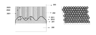
- FIG. 2 is a schematic view showing a structure of a top-emitting white OLED device according to the first embodiment of the disclosure.
- the top-emitting white OLED device includes: a substrate 200 , a first electrode layer 201 formed on the substrate 200 , an organic layer 202 on the first electrode layer 201 , and a second electrode layer 203 on the organic layer 202 .
- a surface of the first electrode layer 201 facing the organic layer 202 has a periodically fluctuated structure.
- the periodically fluctuated structure may be a lattice structure which includes a plurality of continuous bumps 2011 .
- the substrate 200 may include a base substrate, a TFT functional layer and a planarizing layer.
- FIG. 2 shows only a part of one pixel unit.
- FIG. 3 is a schematic view showing a principle of light-emitting enhancement of the top-emitting white OLED device in FIG. 2 .
- a thickness of the organic layer 202 is varied at different positions of the pixel unit.
- a wavelength of red visible light is in a range from 630 to 780 nanometers
- a wavelength of blue visible light is in a range from 420 to 470 nanometers, so an organic layer part 2021 corresponding to the red visible light has a longest cavity length, and an organic layer part 2023 corresponding to the blue visible light has a shortest cavity length.
- an organic layer part 2022 corresponds to visible light of other colors.
- a height difference a 1 between a crest and a trough of the bump 2011 is within a range of a difference of optic cavity lengths corresponding to a variation of a wavelength of visible light, and an interval b 1 (i.e., a period of the crests) between crests (or troughs) of the bumps 2011 is smaller than or equal to a width of the pixel unit.
- the height difference between a crest and a trough of the bump 2011 is in a range from 20 to 150 nanometers, and the interval between the crests (or troughs) of the bumps 2011 is in a range from 1 to 10 micrometers.
- the organic layer 202 may include multiple layers.
- the organic layer 202 may include a hole-injection layer (HIL), a hole-transporting layer, a light-emitting layer, a charge-generating layer, a connecting layer, an electron-transporting layer, an electron-injection layer, a hole-blocking layer, an electron-blocking layer, etc.
- HIL hole-injection layer
- At least one layer (e.g., the HIL) of the organic layer 202 has a large thickness adjustment tolerance, so as to substantially fill up the fluctuated surface of the first electrode layer, so that the organic layer in the pixel unit may have a gradually-varied cavity length.
- the bumps 2011 in the embodiment of the present disclosure are hemispherical or near-hemispherical.
- the bumps 2011 may further be of other shapes.
- the organic layer 104 in the pixel unit has the same thickness (cavity length) at different positions thereof, so a cavity length of an actual light path when viewing at a large angle is longer than that when viewing the OLED device along a direction perpendicular thereto, then a color cast may occur as a result.
- the lattice structure of the first electrode layer 201 has a fluctuated surface, the cavity lengths at different positions where the light is reflected just coincide with a gradually-varied spectrum of the white light OLED device. Even though the viewing angle is large, it may be guaranteed that the cavity lengths at different positions of the pixel are nearly the same. Therefore, the color cast effect may be weaken significantly, and the light intensity may not be decreased significantly.
- FIG. 4 is a schematic view showing a structure of a top-emitting white OLED device according to the second embodiment of the disclosure.
- the OLED device includes: a substrate 200 , a resin layer 204 formed on the substrate 200 , a first electrode layer 201 arranged on the resin layer, an organic layer 202 on the first electrode layer 201 , and a second electrode layer 203 on the organic layer 202 .
- the resin layer 204 is under the first electrode layer 201 , and a surface of the resin layer 204 facing the first electrode layer 201 has a same periodically fluctuated structure as the first electrode layer 201 .
- the substrate 200 may include a base substrate, a TFT functional layer and a planarizing layer.
- the first electrode layer 201 with a reflection function is generally made of metal materials, and a process of forming directly on the substrate 200 the first electrode layer 201 with a lattice structure is difficult. Therefore, in the embodiment of the present disclosure, the resin layer 204 with the lattice structure may be formed on the substrate 200 firstly, to make a model for the first electrode layer 201 . Then the first electrode layer 201 with the same lattice structure as the resin layer 204 is formed on the resin layer 204 , such that the process difficulty may be reduced.
- the resin layer 204 may be made of materials such as polyimide (PI).
- the resin layer 204 for making the model may further be made of other materials easy to make the model.
- FIG. 5 is a top view of a top of a resin layer according to an embodiment of the present disclosure.
- FIG. 6 is a section view of the resin layer according to the embodiment of the present disclosure.
- FIG. 7 is schematic view showing a principle of light-emission enhancement of the top-emitting white OLED device in FIG. 4 .
- a thickness of the organic layer 202 is varied at different positions of the pixel unit.
- a wavelength of red visible light is in a range from 630 to 780 nanometers
- a wavelength of blue visible light is in a range from 420 to 470 nanometers, so an organic layer part 2021 corresponding to the red visible light has a longest cavity length, and an organic layer part 2023 corresponding to the blue visible light has a shortest cavity length.
- an organic layer part 2022 corresponds to visible light of other colors.
- a height difference a 2 between a crest and a trough of the bump 2011 is within a range of a difference of optic cavity lengths corresponding to a variation of a wavelength of visible light, and an interval b 2 (i.e., a period of the crests) between crests (or troughs) of the bumps is smaller than or equal to a width of the pixel unit.
- the height difference between a crest and a trough of the bump 2011 is in a range from 20 to 150 nanometers, and the interval between the crests (or troughs) of the bumps 2011 is in a range from 1 to 10 micrometers.
- the organic layer 202 may include multiple layers.
- the organic layer 202 may include a hole-injection layer (HIL), a hole-transporting layer, a light-emitting layer, a charge-generating layer, a connecting layer, an electron-transporting layer, an electron-injection layer, a hole-blocking layer, an electron-blocking layer, etc.
- HIL hole-injection layer
- At least one layer (e.g., the HIL) of the organic layer 202 has a large thickness adjustment tolerance, so as to substantially fill up the fluctuated surface of the first electrode layer, so that the organic layer in the pixel unit may have a gradually-varied cavity length.
- the second electrode layer 203 on the organic layer 202 has an approximate horizontal state.
- the bumps 2011 in the embodiment of the present disclosure are hemispherical or near-hemispherical.
- the bumps 2011 in the embodiment of the present disclosure may be of other shapes.
- FIG. 8 is a schematic view showing a structure of a top-emitting white OLED device according to this embodiment.
- the difference between the second embodiment and the third embodiment lies in that the lattice structure in the third embodiment includes a plurality of bumps 2011 and pits 2012 arranged at intervals, and a profile of the lattice structure is of a near-sine wave structure.
- a height difference a 3 between a crest and a trough of the bump 2011 is within a range of a difference of optic cavity lengths corresponding to a variation of a wavelength of visible light, and an interval b 3 (i.e., a period of the crests) between crests (or troughs) of the bumps is smaller than or equal to a width of the pixel unit.
- the height difference between a crest and a trough of the bump 2011 is in a range from 20 to 150 nanometers, and the interval between the crests (or troughs) of the bumps 2011 is in a range from 1 to 10 micrometers.
- FIG. 9 is a schematic view showing a structure of a top-emitting white OLED device according to the fourth embodiment of the disclosure.
- a thickness of the organic layer is varied at different positions of the pixel unit.
- the shape of the bottom electrode may not be changed, and the shape of the second electrode layer (i.e., a top electrode) may be changed, i.e., a periodically fluctuated structure (e.g., a lattice structure) is arranged on a surface of the second electrode layer facing the organic layer, such that the cavity length of the organic layer is varied at different positions of the pixel unit.
- a thickness of the organic layer itself may be changed, such that the cavity length of the organic layer is varied at different positions of the pixel unit.
- a light-emitting effect of the top-emitting white OLED device may be improved effectively, and a light intensity may not be decreased obviously and an obvious color cast may not occur when a viewing angle is large.
- the process in the present disclosure is simple, which may make good use of a microcavity effect of metal, so as to improve an external quantum efficiency of the device and reduce a dependency of a display effect of the device on the viewing angle, and especially suitable for a big-size OLED display screen.
- a method for manufacturing an OLED device including a step of forming a plurality of pixel units on a substrate, where each pixel unit includes a first electrode layer, an organic layer and a second electrode layer arranged subsequently on the substrate from bottom up, where the organic layer in each pixel unit includes a gradually-varied cavity length, and the gradually-varied cavity length corresponds to a range from a wavelength of red light to a wavelength of blue light, such that an intensity of white light of the pixel unit is enhanced.
- the method for manufacturing an OLED device includes:
- Step S 11 forming a resin layer on the substrate, where a surface of the resin layer is of a lattice structure, where the lattice structure includes a plurality of continuous bumps, or a plurality of bumps and pits arranged at intervals;
- Step S 12 forming a first electrode layer on the resin layer, where a surface of the first electrode layer has a same lattice structure as the resin layer;
- Step S 13 forming an organic layer on the first electrode layer, with which the fluctuated structure of the first electrode layer is substantially filled up;
- Step S 14 forming a second electrode layer on the organic layer.
- the substrate may include a base substrate, a TFT functional layer and a planarizing layer.
- the resin layer may be formed by the followings two methods.
- Method 1 which includes:
- liquid drop lattice structure subjecting the liquid drop lattice structure to a cross-linked polymerization, so as to form the resin layer with the lattice structure after the liquid drop lattice structure is cured.
- Method 2 which includes:
- the method for manufacturing an OLED device according to the embodiment of the present disclosure may include ( FIG. 4 shows a structure of the OLED device manufactured by this method):
- each of the cured resin bump is hemispherical or near-hemispherical, a height difference between a crest and a trough of the bump is in a range from 20 to 150 nanometers, and an interval between the crests or troughs of the bumps is in a range from 1 to 10 micrometers;
- the method of forming the organic layer includes wet coating (e.g., spin coating and printing), dry distillation or a combination thereof, where the wet coating is preferable, which may cause the pits to be filled up better; and
- a second electrode layer on the organic layer (i.e., a top electrode) and packaging the OLED device.
- FIG. 6 shows a structure of the OLED device manufactured by this method
- a resin layer on a planarizing layer by means of coating, exposing and developing the resin layer by using a photomask, and using the exposing process to form a lattice structure with hemispherical bumps and bowl-like pits arranged at intervals, wherein a height difference between a crest and a trough of the bump is in a range of 20 to 150 nanometers, and a periodical interval is in a range from 1 to 10 micrometers;
- the method of forming the organic layer includes wet coating (e.g., spin coating and printing), dry distillation or a combination thereof, where the wet coating is preferable, which may cause the pits to be filled up better; and
- a second electrode layer on the organic layer (i.e., a top electrode) and packaging the OLED device.
- a display apparatus is further provided by the present disclosure, including the top-emitting white OLED device hereinabove.
- the display apparatus may be any product or component with display function, such as OLED panels, cell phones, tablet PCs, televisions, displayers, laptops, digital photo frames and navigators.
Landscapes
- Physics & Mathematics (AREA)
- Optics & Photonics (AREA)
- Engineering & Computer Science (AREA)
- Manufacturing & Machinery (AREA)
- Electroluminescent Light Sources (AREA)
Abstract
The present disclosure provides a top-emitting white organic light emitting diode (OLED) device, a method for manufacturing the same and a display apparatus. The OLED device includes a plurality of pixel units on a substrate, wherein each pixel unit includes a first electrode layer, an organic layer and a second electrode layer arranged subsequently on the substrate from bottom up, and the organic layer in each pixel unit includes a gradually-varied cavity length, and the gradually-varied cavity length corresponds to a range from a wavelength of red light to a wavelength of blue light.
Description
This application is the U.S. national phase of PCT Application No. PCT/CN2015/073671 filed on Mar. 5, 2015, which claims a priority of the Chinese Patent Application No. 201410640299.7 filed on Nov. 13, 2014, the disclosures of which are incorporated in their entirety by reference.
The present disclosure relates to the field of organic light-emitting diode (OLED) display technology, and in particular to a top-emitting white OLED device, a method for manufacturing the same and a display apparatus.
An organic light-emitting diode (OLED) is called as a third-generation dreamlike display technology as it has the following advantages: active light-emitting, good temperature characteristic, low power consumption, fast response, being flexible, ultra light and thin, and low cost. At present, with the continuous funding, research and development of manufacturers all over the world, an OLED panel display technology is becoming a more and more mature mass production technology, and a market requirement thereof is growing rapidly.
There are mainly two kinds of OLEDs in terms of light-emitting direction, i.e., a bottom-emitting OLED and a top-emitting OLED. The bottom-emitting OLED refers to an OLED where light is emitted from a substrate, and the top-emitting OLED refers to an OLED where light is emitted from a top of a device. The top-emitting OLED may not be influenced whether light can pass through the substrate or not, therefore an aperture ratio of a display panel may be improved effectively, thereby expanding a thin film transistor (TFT) circuit design of the substrate and expanding a scope of electrode materials to be selected, which is beneficial to an integration of the device and the TFT circuit.
Although the OLED may improve device efficiency, narrow a spectrum and improve color purity, the OLED generally is of a strong microcavity effect. Due to the microcavity effect, an electroluminescence spectrum of the OLED may vary with a viewing angle, and an efficiency of the OLED may decrease significantly when the viewing angle is large, i.e., the efficiency of the OLED may depend on the viewing angle due to the microcavity effect, which is an obvious disadvantage for a high-precision panel display.
In view of this, the present disclosure provides a top-emitting white OLED device, a method for manufacturing the same, and a display apparatus, so as to solve the issue in the related art that the larger the viewing angle is, the worse an effect of light-emitting of the top-emitting white OLED may be due to the microcavity effect.
To solve the above technical issues, a top-emitting white organic light emitting diode (OLED) device is provided by the present disclosure, including a plurality of pixel units on a substrate. Each pixel unit includes a first electrode layer, an organic layer and a second electrode layer arranged subsequently on the substrate from bottom up. The organic layer in each pixel unit comprises a gradually-varied cavity length, and the gradually-varied cavity length corresponds to a range from a wavelength of red light to a wavelength of blue light.
Alternatively, a surface of the first electrode layer facing the organic layer has a periodically fluctuated structure.
Alternatively, the periodically fluctuated structure is a lattice structure, which includes a plurality of continuous bumps or a plurality of bumps and pits arranged at intervals.
Alternatively, a height difference between a crest and a trough of the bump is within a range of a difference of optic cavity lengths corresponding to a variation of a wavelength of visible light, and an interval between crests or troughs of the bumps is smaller than or equal to a width of the pixel unit.
Alternatively, the height difference between the crest and the trough of the bump is in a range from 20 to 150 nanometers, and the interval between the crests or troughs of the bumps is in a range from 1 to 10 micrometers.
Alternatively, the bumps are hemispherical or near-hemispherical, and the pits are hemispherical or near-hemispherical.
Alternatively, a profile of the lattice structure is a near-sine wave when the lattice structure includes a plurality of bumps and pits arranged at intervals.
Alternatively, the top-emitting white OLED device further includes a resin layer under the first electrode layer, where a surface of the resin layer facing the first electrode layer has a same periodically fluctuated structure as the first electrode layer. Alternatively, the resin layer includes polyimide.
Alternatively, the periodically fluctuated structure of the first electrode layer is substantially filled up with the organic layer.
Alternatively, the first electrode layer is a reflective electrode, and the second electrode layer is a transflective electrode.
A method for manufacturing a top-emitting white OLED device is further provided, including a step of forming a plurality of pixel units on a substrate. Each pixel unit includes a first electrode layer, an organic layer and a second electrode layer arranged subsequently on the substrate from bottom up, where the organic layer in each pixel unit includes a gradually-varied cavity length, and the gradually-varied cavity length corresponds to a range from a wavelength of red light to a wavelength of blue light.
Alternatively, the method further includes:
forming a resin layer on the substrate, where a surface of the resin layer is of a lattice structure which the lattice includes a plurality of continuous bumps or a plurality of bumps and pits arranged at intervals;
forming a first electrode layer on the resin layer, where a surface of the first electrode layer has the same lattice structure as the resin layer;
forming an organic layer on the first electrode layer, with which the fluctuated structure of the first electrode layer is substantially filled up; and
forming a second electrode layer on the organic layer.
Alternatively, in the lattice structure of the resin layer, the bumps are hemispherical or near-hemispherical, where a height difference between a crest and a trough of the bump is in a range from 20 to 150 nanometers, and an interval between the crests or troughs of the bumps is in a range from 1 to 10 micrometers.
Alternatively, the step of forming the resin layer on the substrate includes:
coating a precursor ink configured to form a resin onto the substrate by means of printing, to form a uniform liquid drop lattice structure, and removing a solvent from the liquid drop lattice and subjecting the liquid drop lattice structure to a cross-linked polymerization, so as to form the resin layer with the lattice structure after the liquid drop lattice is cured.
Alternatively, the step of forming the resin layer on the substrate includes:
forming a resin film on the substrate by means of coating; and
exposing and developing the resin film by using a photomask, to form the resin layer with a lattice structure.
A display apparatus is further provided by the present disclosure, including the top-emitting white OLED device hereinabove.
The technical scheme of the present disclosure has the following advantages: in the top-emitting white OLED device, a cavity length of an organic layer of a pixel unit is gradually-varied, and the gradually-varied cavity length corresponds to a range from a wavelength of red light to a wavelength of blue light, so that the cavity length enhancing the microcavity is varied at different positions of the organic layer, thus an intensity of white light of the pixel unit may be enhanced.
To make the technical problem, technical solution and advantages of the present disclosure more clear, the present disclosure will be described in details in conjunction with embodiments and drawings.
As shown in FIG. 1 , the organic layer 104 in a pixel unit has the same cavity length at different locations thereof. Due to a microcavity effect, an intensity of only a kind of visible light which has an optimum wavelength may be enhanced, while visible light of other wavelengths may be filtered out, such that a light intensity may be decreased when a viewing angle is large.
In view of this, a top-emitting white OLED device is provided by the present disclosure, including a plurality of pixel units on a substrate, where each pixel unit includes a first electrode layer, an organic layer and a second electrode layer subsequently arranged on the substrate from bottom up. The organic layer in each pixel unit includes a gradually-varied cavity length (i.e., thickness), and the gradually-varied cavity length corresponds to a range from a wavelength of red light to a wavelength of blue light, such that an intensity of white light of the pixel unit may be enhanced.
In an embodiment of the present disclosure, the organic layer in the pixel unit has the gradually-varied cavity length, and the gradually-varied cavity length corresponds to the range from the wavelength of red light to the wavelength of blue light. Therefore, different positions of the organic layer correspond to different microcavity-enhanced cavity lengths, and then an emission intensity of white light of the pixel unit may be enhanced.
In the embodiment of the present disclosure, the first electrode layer is a bottom electrode (generally as an anode), and the second electrode layer is a top electrode (generally as a cathode). The first electrode layer is a reflective electrode, and materials thereof may include one of gold, silver and aluminum or an alloy of them. The second electrode layer is a transflective electrode, and materials thereof may include gold, silver or an alloy of them.
The top-emitting white OLED device in the embodiment of the present disclosure may be of various structures. The structure of the top-emitting white OLED device may be illustrated in the following.
The substrate 200 may include a base substrate, a TFT functional layer and a planarizing layer.
Alternatively, a height difference a1 between a crest and a trough of the bump 2011 is within a range of a difference of optic cavity lengths corresponding to a variation of a wavelength of visible light, and an interval b1 (i.e., a period of the crests) between crests (or troughs) of the bumps 2011 is smaller than or equal to a width of the pixel unit.
In order to enhance the white light intensity effectively, alternatively, the height difference between a crest and a trough of the bump 2011 is in a range from 20 to 150 nanometers, and the interval between the crests (or troughs) of the bumps 2011 is in a range from 1 to 10 micrometers.
In the embodiment of the present disclosure, the organic layer 202 may include multiple layers. For example, the organic layer 202 may include a hole-injection layer (HIL), a hole-transporting layer, a light-emitting layer, a charge-generating layer, a connecting layer, an electron-transporting layer, an electron-injection layer, a hole-blocking layer, an electron-blocking layer, etc. At least one layer (e.g., the HIL) of the organic layer 202 has a large thickness adjustment tolerance, so as to substantially fill up the fluctuated surface of the first electrode layer, so that the organic layer in the pixel unit may have a gradually-varied cavity length.
Alternatively, the bumps 2011 in the embodiment of the present disclosure are hemispherical or near-hemispherical. Alternatively, the bumps 2011 may further be of other shapes.
As shown in FIG. 1 , the organic layer 104 in the pixel unit has the same thickness (cavity length) at different positions thereof, so a cavity length of an actual light path when viewing at a large angle is longer than that when viewing the OLED device along a direction perpendicular thereto, then a color cast may occur as a result.
In the embodiment of the present disclosure, since the lattice structure of the first electrode layer 201 has a fluctuated surface, the cavity lengths at different positions where the light is reflected just coincide with a gradually-varied spectrum of the white light OLED device. Even though the viewing angle is large, it may be guaranteed that the cavity lengths at different positions of the pixel are nearly the same. Therefore, the color cast effect may be weaken significantly, and the light intensity may not be decreased significantly.
The substrate 200 may include a base substrate, a TFT functional layer and a planarizing layer.
The first electrode layer 201 with a reflection function is generally made of metal materials, and a process of forming directly on the substrate 200 the first electrode layer 201 with a lattice structure is difficult. Therefore, in the embodiment of the present disclosure, the resin layer 204 with the lattice structure may be formed on the substrate 200 firstly, to make a model for the first electrode layer 201. Then the first electrode layer 201 with the same lattice structure as the resin layer 204 is formed on the resin layer 204, such that the process difficulty may be reduced.
The resin layer 204 may be made of materials such as polyimide (PI). Alternatively, the resin layer 204 for making the model may further be made of other materials easy to make the model.
Alternatively, a height difference a2 between a crest and a trough of the bump 2011 is within a range of a difference of optic cavity lengths corresponding to a variation of a wavelength of visible light, and an interval b2 (i.e., a period of the crests) between crests (or troughs) of the bumps is smaller than or equal to a width of the pixel unit.
In order to enhance the white light intensity effectively, Alternatively the height difference between a crest and a trough of the bump 2011 is in a range from 20 to 150 nanometers, and the interval between the crests (or troughs) of the bumps 2011 is in a range from 1 to 10 micrometers.
In the embodiment of the present disclosure, the organic layer 202 may include multiple layers. For example, the organic layer 202 may include a hole-injection layer (HIL), a hole-transporting layer, a light-emitting layer, a charge-generating layer, a connecting layer, an electron-transporting layer, an electron-injection layer, a hole-blocking layer, an electron-blocking layer, etc. At least one layer (e.g., the HIL) of the organic layer 202 has a large thickness adjustment tolerance, so as to substantially fill up the fluctuated surface of the first electrode layer, so that the organic layer in the pixel unit may have a gradually-varied cavity length.
In the embodiment of the present disclosure, due to the process, it may be difficult to completely fill up the fluctuated surface of the first electrode layer with the organic layer 202, and the fluctuated surface of the first electrode layer may be filled up with the organic layer 202 partially. Therefore, the second electrode layer 203 on the organic layer 202 has an approximate horizontal state.
Alternatively, the bumps 2011 in the embodiment of the present disclosure are hemispherical or near-hemispherical. Alternatively, the bumps 2011 in the embodiment of the present disclosure may be of other shapes.
Alternatively, a height difference a3 between a crest and a trough of the bump 2011 is within a range of a difference of optic cavity lengths corresponding to a variation of a wavelength of visible light, and an interval b3 (i.e., a period of the crests) between crests (or troughs) of the bumps is smaller than or equal to a width of the pixel unit.
In order to enhance the white light intensity effectively, Alternatively the height difference between a crest and a trough of the bump 2011 is in a range from 20 to 150 nanometers, and the interval between the crests (or troughs) of the bumps 2011 is in a range from 1 to 10 micrometers.
Alternatively, the bumps 2011 in the embodiment of the present disclosure are hemispherical or near-hemispherical, and the pits 2012 in the embodiment of the present disclosure are hemispherical or near-hemispherical. Alternatively, the bumps 2011 and the pits 2012 may be of other shapes. FIG. 9 is a schematic view showing a structure of a top-emitting white OLED device according to the fourth embodiment of the disclosure.
In the embodiment of the present disclosure, by changing the shape of the first electrode layer (i.e., a bottom electrode) of the top-emitting white OLED device, a thickness of the organic layer is varied at different positions of the pixel unit. Alternatively, the shape of the bottom electrode may not be changed, and the shape of the second electrode layer (i.e., a top electrode) may be changed, i.e., a periodically fluctuated structure (e.g., a lattice structure) is arranged on a surface of the second electrode layer facing the organic layer, such that the cavity length of the organic layer is varied at different positions of the pixel unit. Alternatively, a thickness of the organic layer itself may be changed, such that the cavity length of the organic layer is varied at different positions of the pixel unit.
The OLED device in the embodiment of the present disclosure has the following advantages:
(1) a light-emitting effect of the top-emitting white OLED device may be improved effectively, and a light intensity may not be decreased obviously and an obvious color cast may not occur when a viewing angle is large.
(2) the process in the present disclosure is simple, which may make good use of a microcavity effect of metal, so as to improve an external quantum efficiency of the device and reduce a dependency of a display effect of the device on the viewing angle, and especially suitable for a big-size OLED display screen.
A method for manufacturing an OLED device is further provided in the present disclosure, including a step of forming a plurality of pixel units on a substrate, where each pixel unit includes a first electrode layer, an organic layer and a second electrode layer arranged subsequently on the substrate from bottom up, where the organic layer in each pixel unit includes a gradually-varied cavity length, and the gradually-varied cavity length corresponds to a range from a wavelength of red light to a wavelength of blue light, such that an intensity of white light of the pixel unit is enhanced.
Alternatively, the method for manufacturing an OLED device includes:
Step S11: forming a resin layer on the substrate, where a surface of the resin layer is of a lattice structure, where the lattice structure includes a plurality of continuous bumps, or a plurality of bumps and pits arranged at intervals;
Step S12: forming a first electrode layer on the resin layer, where a surface of the first electrode layer has a same lattice structure as the resin layer;
Step S13: forming an organic layer on the first electrode layer, with which the fluctuated structure of the first electrode layer is substantially filled up; and
Step S14: forming a second electrode layer on the organic layer.
The substrate may include a base substrate, a TFT functional layer and a planarizing layer.
The resin layer may be formed by the followings two methods.
Method 1, which includes:
coating a precursor ink configured to form a resin onto the substrate by means of printing, to form a uniform liquid drop lattice structure,
removing a solvent from the liquid drop lattice structure,
subjecting the liquid drop lattice structure to a cross-linked polymerization, so as to form the resin layer with the lattice structure after the liquid drop lattice structure is cured.
Method 2, which includes:
forming a resin film on the substrate by means of coating; and
exposing and developing the resin film by using a photomask, to form the resin layer with a lattice structure.
The method for manufacturing an OLED device according to the embodiment of the present disclosure may include (FIG. 4 shows a structure of the OLED device manufactured by this method):
(1) coating a precursor ink configured to form a resin onto the substrate by means of printing, to form a uniform liquid drop lattice structure, removing a solvent from the liquid drop lattice structure and subjecting the liquid drop lattice structure to a cross-linked polymerization, so as to form the resin layer with a layer of lattice structure after the liquid drop lattice structure is cured, wherein each of the cured resin bump is hemispherical or near-hemispherical, a height difference between a crest and a trough of the bump is in a range from 20 to 150 nanometers, and an interval between the crests or troughs of the bumps is in a range from 1 to 10 micrometers;
(2) depositing a first electrode layer (i.e., a bottom electrode) on the resin layer, and maintaining a fluctuated structure of the resin layer;
(3) depositing an organic layer on the first electrode layer, wherein at least one layer (e.g., a hole-injection layer) of the organic layer has a large thickness adjustment tolerance, which may cause the fluctuated structure of the first electrode layer to be substantially filled up, such that a thickness of the organic layer between the two electrode layers may be varied with the fluctuated of the bottom electrode. The method of forming the organic layer includes wet coating (e.g., spin coating and printing), dry distillation or a combination thereof, where the wet coating is preferable, which may cause the pits to be filled up better; and
(4) depositing a second electrode layer on the organic layer (i.e., a top electrode) and packaging the OLED device.
Another method for manufacturing an OLED device according to the embodiment of the present disclosure includes (FIG. 6 shows a structure of the OLED device manufactured by this method):
(1) forming a resin layer on a planarizing layer by means of coating, exposing and developing the resin layer by using a photomask, and using the exposing process to form a lattice structure with hemispherical bumps and bowl-like pits arranged at intervals, wherein a height difference between a crest and a trough of the bump is in a range of 20 to 150 nanometers, and a periodical interval is in a range from 1 to 10 micrometers;
(2) depositing a first electrode layer (i.e., a bottom electrode) on the resin layer, and maintaining a fluctuated structure of the resin layer;
(3) depositing an organic layer on the first electrode layer, wherein at least one layer (e.g., a hole-injection layer) of the organic layer has a large thickness adjustment tolerance, which may cause the fluctuated structure of the first electrode layer to be filled up, such that a thickness of the organic layer between the two electrode layers may be varied with the fluctuated of the bottom electrode. The method of forming the organic layer includes wet coating (e.g., spin coating and printing), dry distillation or a combination thereof, where the wet coating is preferable, which may cause the pits to be filled up better; and
(4) depositing a second electrode layer on the organic layer (i.e., a top electrode) and packaging the OLED device.
A display apparatus is further provided by the present disclosure, including the top-emitting white OLED device hereinabove. The display apparatus may be any product or component with display function, such as OLED panels, cell phones, tablet PCs, televisions, displayers, laptops, digital photo frames and navigators.
The above are the preferable embodiments of the present disclosure. It should be noted that, those skilled in the art may make several improvements and modifications without departing from the principle of the present disclosure, and these improvements and modifications may also fall into the scope of the present disclosure.
Claims (13)
1. A top-emitting white organic light emitting diode (OLED) device, comprising a plurality of pixel units on a substrate, wherein
each pixel unit comprises a first electrode layer, an organic layer and a second electrode layer arranged subsequently on the substrate from bottom up,
the organic layer in each pixel unit has a flat upper surface, a continuously-varied thickness and a gradually-varied cavity length, and the gradually-varied cavity length corresponds to a range from a wavelength of red light to a wavelength of blue light, and
wherein a surface of the first electrode layer facing the organic layer has a periodically fluctuated structure, the periodically fluctuated structure being a lattice structure, which comprises a plurality of continuous bumps, or a plurality of bumps and pits arranged at intervals in two different directions, front to back and side to side, the bumps being hemispherical or near-hemispherical, and the pits being hemispherical.
2. The top-emitting white OLED device according to claim 1 , wherein
a height difference between a crest and a trough of the bump is within a range of a difference of optic cavity lengths corresponding to a variation of a wavelength of visible light, and
an interval between crests or troughs of the bumps is smaller than or equal to a width of the pixel unit.
3. The top-emitting white OLED device according to claim 2 , wherein
the height difference between the crest and the trough of the bump is in a range from 20 to 150 nanometers, and
the interval between the crests or troughs of the bumps is in a range from 1 to 10 micrometers.
4. The top-emitting white OLED device according to claim 1 , wherein a profile of the lattice structure is a near-sine wave when the lattice structure comprises a plurality of bumps and pits arranged at intervals.
5. The top-emitting white OLED device according to claim 1 , further comprising a resin layer under the first electrode layer,
wherein a surface of the resin layer facing the first electrode layer has a same periodically fluctuated structure as the first electrode layer.
6. The top-emitting white OLED device according to claim 5 , wherein the resin layer comprises polyimide.
7. The top-emitting white OLED device according to claim 1 , wherein the periodically fluctuated structure of the first electrode layer is substantially filled up with the organic layer.
8. The top-emitting white OLED device according to claim 1 , wherein the first electrode layer is a reflective electrode, and the second electrode layer is a transflective electrode.
9. A display apparatus, comprising the top-emitting white OLED device according to claim 1 .
10. A method for manufacturing a top-emitting white OLED device, comprising a step of:
forming a plurality of pixel units on a substrate, wherein
each pixel unit comprises a first electrode layer, an organic layer and a second electrode layer arranged subsequently on the substrate from bottom up, and
the organic layer in each pixel unit has a flat upper surface, a continuously-varied thickness and a gradually-varied cavity length, and the gradually-varied cavity length corresponds to a range from a wavelength of red light to a wavelength of blue light;
the method further comprising:
forming a resin layer on the substrate, wherein a surface of the resin layer is of a lattice structure comprising a plurality of continuous bumps or a plurality of bumps and pits arranged at intervals in two different directions, front to back and side to side;
forming a first electrode layer on the resin layer, a surface of the first electrode layer having a same lattice structure as the resin layer;
forming an organic layer on the first electrode layer, with which a fluctuated structure of the first electrode layer is substantially filled up; and
forming a second electrode layer on the organic layer,
wherein the bumps are hemispherical in the lattice structure of the resin layer.
11. The method according to claim 10 , wherein
a height difference between a crest and a trough of the bump is in a range from 20 to 150 nanometers, and
an interval between the crests or troughs of the bumps is in a range from 1 to 10 micrometers.
12. The method according to claim 10 , wherein the step of forming the resin layer on the substrate comprises:
coating a precursor ink configured to form a resin onto the substrate by means of printing, to form a uniform liquid drop lattice structure,
removing a solvent from the liquid drop lattice structure, and
subjecting the liquid drop lattice structure to a cross-linked polymerization, so as to form the resin layer with the lattice structure after the liquid drop lattice structure is cured.
13. The method according to claim 10 , wherein the step of forming the resin layer on the substrate comprises:
forming a resin film on the substrate by means of coating; and
exposing and developing the resin film by using a photomask, to form the resin layer with a lattice structure.
Applications Claiming Priority (4)
| Application Number | Priority Date | Filing Date | Title |
|---|---|---|---|
| CN201410640299 | 2014-11-13 | ||
| CN201410640299.7 | 2014-11-13 | ||
| CN201410640299.7A CN104319352B (en) | 2014-11-13 | 2014-11-13 | A kind of top emitting white light OLED device and preparation method thereof, display device |
| PCT/CN2015/073671 WO2016074378A1 (en) | 2014-11-13 | 2015-03-05 | Top-emitting white light oled device and manufacturing method thereof, and display device |
Publications (2)
| Publication Number | Publication Date |
|---|---|
| US20160343967A1 US20160343967A1 (en) | 2016-11-24 |
| US10186675B2 true US10186675B2 (en) | 2019-01-22 |
Family
ID=52374557
Family Applications (1)
| Application Number | Title | Priority Date | Filing Date |
|---|---|---|---|
| US14/888,736 Active 2035-04-10 US10186675B2 (en) | 2014-11-13 | 2015-03-05 | Top-emitting white organic light emitting diode device, method for manufacturing the same, and display apparatus |
Country Status (3)
| Country | Link |
|---|---|
| US (1) | US10186675B2 (en) |
| CN (1) | CN104319352B (en) |
| WO (1) | WO2016074378A1 (en) |
Cited By (1)
| Publication number | Priority date | Publication date | Assignee | Title |
|---|---|---|---|---|
| US20180076270A1 (en) * | 2016-09-13 | 2018-03-15 | Samsung Display Co., Ltd . | Display device |
Families Citing this family (8)
| Publication number | Priority date | Publication date | Assignee | Title |
|---|---|---|---|---|
| CN104319352B (en) | 2014-11-13 | 2018-02-13 | 京东方科技集团股份有限公司 | A kind of top emitting white light OLED device and preparation method thereof, display device |
| CN105629378B (en) | 2016-01-04 | 2018-03-16 | 京东方科技集团股份有限公司 | Display base plate and display device |
| FR3065324A1 (en) * | 2017-04-12 | 2018-10-19 | Commissariat A L'energie Atomique Et Aux Energies Alternatives | PIXEL OF A MICRO-SCREEN WITH ORGANIC ELECTROLUMINESCENT DIODES |
| CN108933154B (en) | 2017-05-26 | 2021-04-27 | 京东方科技集团股份有限公司 | Preparation method of organic light-emitting diode display substrate, display substrate and display device |
| CN107364248B (en) * | 2017-06-29 | 2019-04-09 | 华南理工大学 | A kind of method of inkjet printing film and substrate interface observation and regulation |
| CN110214377B (en) | 2017-11-23 | 2021-09-24 | 京东方科技集团股份有限公司 | Organic light emitting diode assembly, light source and method for manufacturing organic light emitting diode assembly |
| CN109148730A (en) * | 2018-09-05 | 2019-01-04 | 京东方科技集团股份有限公司 | Display panel and its manufacturing method, display device |
| JP2022137935A (en) * | 2021-03-09 | 2022-09-22 | 本田技研工業株式会社 | Car body structure having head-up display |
Citations (18)
| Publication number | Priority date | Publication date | Assignee | Title |
|---|---|---|---|---|
| US20050280364A1 (en) * | 2004-06-18 | 2005-12-22 | Tetsuji Omura | Electroluminescence panel |
| US20070096636A1 (en) * | 2005-10-28 | 2007-05-03 | Samsung Electronics Co., Ltd | Organic light emitting diode display and method of manufacturing the same |
| US20070159086A1 (en) | 2005-12-28 | 2007-07-12 | Gang Yu | Organic electronic device with microcavity structure |
| CN101013745A (en) | 2006-02-03 | 2007-08-08 | 索尼株式会社 | Display device and display unit |
| US20080122347A1 (en) * | 2006-11-27 | 2008-05-29 | Lee Baek-Woon | Organic light emitting device with increased luminscence |
| US20090051275A1 (en) | 2007-08-21 | 2009-02-26 | Seiko Epson Corporation | Light emitting device |
| US20090085477A1 (en) * | 2007-10-02 | 2009-04-02 | Samsung Electronics Co., Ltd. | Organic light emitting diode display |
| US20090115326A1 (en) * | 2007-11-02 | 2009-05-07 | Tpo Displays Corp. | Organic light emitting display device and electronic device |
| US20100289727A1 (en) * | 2009-05-12 | 2010-11-18 | Miller Michael E | Electro-luminescent display with adjustable white point |
| US20110303905A1 (en) * | 2008-12-09 | 2011-12-15 | Malte Gather | Organic Light-Emitting Diode Having Optical Resonator in Addition to Production Method |
| CN102362368A (en) | 2009-03-03 | 2012-02-22 | 富士胶片株式会社 | Method for producing light-emitting display device, light-emitting display device and light-emitting display |
| US20120187435A1 (en) * | 2009-04-02 | 2012-07-26 | Saint-Gobain Glass France | Method for manufacturing a structure with a textured surface as a mounting for an organic light-emitting diode device, and oled structure with a textured surface |
| WO2013187149A1 (en) | 2012-06-11 | 2013-12-19 | Jx日鉱日石エネルギー株式会社 | Organic el element and method for manufacturing same |
| CN103811669A (en) | 2012-11-09 | 2014-05-21 | 上海天马微电子有限公司 | Organic luminescent device, and organic light emitting diode display apparatus and manufacturing method thereof |
| US20140151651A1 (en) | 2012-12-05 | 2014-06-05 | Samsung Display Co., Ltd. | Organic light emitting diode display device and method of manufacturing the same |
| CN104319352A (en) | 2014-11-13 | 2015-01-28 | 京东方科技集团股份有限公司 | Top emission white light OLED device, preparation method of top emission white light OLED device, and display device |
| CN204179111U (en) | 2014-11-13 | 2015-02-25 | 京东方科技集团股份有限公司 | A kind of top emitting white light OLED device and display unit |
| US20150187858A1 (en) * | 2013-12-31 | 2015-07-02 | Shanghai Tianma AM-OLED Co., Ltd. | Oled display panel and method of manufacturing the same and display apparatus |
-
2014
- 2014-11-13 CN CN201410640299.7A patent/CN104319352B/en active Active
-
2015
- 2015-03-05 US US14/888,736 patent/US10186675B2/en active Active
- 2015-03-05 WO PCT/CN2015/073671 patent/WO2016074378A1/en active Application Filing
Patent Citations (20)
| Publication number | Priority date | Publication date | Assignee | Title |
|---|---|---|---|---|
| US20050280364A1 (en) * | 2004-06-18 | 2005-12-22 | Tetsuji Omura | Electroluminescence panel |
| US20070096636A1 (en) * | 2005-10-28 | 2007-05-03 | Samsung Electronics Co., Ltd | Organic light emitting diode display and method of manufacturing the same |
| US20070159086A1 (en) | 2005-12-28 | 2007-07-12 | Gang Yu | Organic electronic device with microcavity structure |
| CN101013745A (en) | 2006-02-03 | 2007-08-08 | 索尼株式会社 | Display device and display unit |
| US20080122347A1 (en) * | 2006-11-27 | 2008-05-29 | Lee Baek-Woon | Organic light emitting device with increased luminscence |
| US20090051275A1 (en) | 2007-08-21 | 2009-02-26 | Seiko Epson Corporation | Light emitting device |
| US20090085477A1 (en) * | 2007-10-02 | 2009-04-02 | Samsung Electronics Co., Ltd. | Organic light emitting diode display |
| US20090115326A1 (en) * | 2007-11-02 | 2009-05-07 | Tpo Displays Corp. | Organic light emitting display device and electronic device |
| TW200922371A (en) | 2007-11-02 | 2009-05-16 | Tpo Displays Corp | Organic light emitting display device and electronic device |
| US20110303905A1 (en) * | 2008-12-09 | 2011-12-15 | Malte Gather | Organic Light-Emitting Diode Having Optical Resonator in Addition to Production Method |
| CN102362368A (en) | 2009-03-03 | 2012-02-22 | 富士胶片株式会社 | Method for producing light-emitting display device, light-emitting display device and light-emitting display |
| US20120187435A1 (en) * | 2009-04-02 | 2012-07-26 | Saint-Gobain Glass France | Method for manufacturing a structure with a textured surface as a mounting for an organic light-emitting diode device, and oled structure with a textured surface |
| US20100289727A1 (en) * | 2009-05-12 | 2010-11-18 | Miller Michael E | Electro-luminescent display with adjustable white point |
| WO2013187149A1 (en) | 2012-06-11 | 2013-12-19 | Jx日鉱日石エネルギー株式会社 | Organic el element and method for manufacturing same |
| US20150060840A1 (en) * | 2012-06-11 | 2015-03-05 | Jx Nippon Oil & Energy Corporation | Organic el element and method for manufacturing same |
| CN103811669A (en) | 2012-11-09 | 2014-05-21 | 上海天马微电子有限公司 | Organic luminescent device, and organic light emitting diode display apparatus and manufacturing method thereof |
| US20140151651A1 (en) | 2012-12-05 | 2014-06-05 | Samsung Display Co., Ltd. | Organic light emitting diode display device and method of manufacturing the same |
| US20150187858A1 (en) * | 2013-12-31 | 2015-07-02 | Shanghai Tianma AM-OLED Co., Ltd. | Oled display panel and method of manufacturing the same and display apparatus |
| CN104319352A (en) | 2014-11-13 | 2015-01-28 | 京东方科技集团股份有限公司 | Top emission white light OLED device, preparation method of top emission white light OLED device, and display device |
| CN204179111U (en) | 2014-11-13 | 2015-02-25 | 京东方科技集团股份有限公司 | A kind of top emitting white light OLED device and display unit |
Non-Patent Citations (7)
| Title |
|---|
| First Office Action regarding Chinese application No. 201410640299.7, dated Mar. 22, 2016. Translation provided by Dragon Intellectual Property Law Firm. |
| S. Hofmann, M. Thomschke, B. Lüssem, and K. Leo, "Top-emitting organic light-emitting diodes," Opt. Express 19, A1250-A1264 (2011). * |
| Second Office Action regarding Chinese application No. 201410640299.7, dated Oct. 31, 2016. Translation provided by Dragon Intellectual Property Law Firm. |
| Third Office Action regarding Chinese Application No. 201410640299.7, dated Apr. 24, 2017. Translation provided by Dragon Intellectual Property Law Firm. |
| Written Opinion of the International Searching Authority for international application No. PCT/CN2015/073671. |
| Yue-Feng Liu et al., Viewing-angle independence of white emission from microcavity top-emitting organic light-emitting devices with periodically and gradually changed cavity length, In Organic Electronics, vol. 14, Issue 6, 2013, pp. 1597-1601. * |
| Yue-Feng Liu, Jing Feng, Yan-Gang Bi, Jun-Feng Song, Yu Jin, Yu Bai, Qi-Dai Chen, and Hong-Bo Sun, "Omnidirectional emission from top-emitting organic light-emitting devices with microstructured cavity," Opt. Lett. 37, 124-126 (2012). * |
Cited By (4)
| Publication number | Priority date | Publication date | Assignee | Title |
|---|---|---|---|---|
| US20180076270A1 (en) * | 2016-09-13 | 2018-03-15 | Samsung Display Co., Ltd . | Display device |
| US10707285B2 (en) * | 2016-09-13 | 2020-07-07 | Samsung Display Co., Ltd. | Display device |
| US11183548B2 (en) | 2016-09-13 | 2021-11-23 | Samsung Display Co., Ltd. | Display device |
| US11895875B2 (en) | 2016-09-13 | 2024-02-06 | Samsung Display Co., Ltd. | Display device |
Also Published As
| Publication number | Publication date |
|---|---|
| WO2016074378A1 (en) | 2016-05-19 |
| US20160343967A1 (en) | 2016-11-24 |
| CN104319352B (en) | 2018-02-13 |
| CN104319352A (en) | 2015-01-28 |
Similar Documents
| Publication | Publication Date | Title |
|---|---|---|
| US10186675B2 (en) | Top-emitting white organic light emitting diode device, method for manufacturing the same, and display apparatus | |
| US10826028B2 (en) | Manufacture method of flexible display panel | |
| EP3242344B1 (en) | Organic light-emitting diode array substrate, manufacturing method therefor, and display device | |
| WO2015143840A1 (en) | Organic electroluminescence display panel and manufacturing method therefor and display device | |
| US20150318447A1 (en) | Display Apparatus and Method of Manufacturing the Same | |
| WO2020030042A1 (en) | Oled display substrate and manufacturing method therefor, and display apparatus | |
| US20170133614A1 (en) | Light-Emiting Device and Manufacturing Method Therefor, Display Apparatus, and Optical Detection Apparatus | |
| US20160284673A1 (en) | Full-color light emitting diode (led) display panel, method of manufacturing full-color led display panel, display device | |
| WO2016123943A1 (en) | Array substrate and manufacturing method thereof, and display device | |
| EP3605612B1 (en) | Pixel defining layer, organic light-emitting device and preparation method thereof, and display device | |
| US10038159B2 (en) | Organic electroluminescent device structure and manufacturing for the same | |
| TWI511341B (en) | A method of making organic light emitting diode | |
| US20150014667A1 (en) | Oled device and manufacturing method thereof, display apparatus | |
| WO2018120710A1 (en) | Oled display panel, method for manufacturing same, and display device | |
| US20210335928A1 (en) | Array substrate, manufacturing method thereof, and display apparatus | |
| CN104319351A (en) | OLED array substrate, preparation method of OLED array substrate, display panel and display device | |
| CN208655656U (en) | Pixel defining layer, display base plate, display panel and display device | |
| CN102226998A (en) | Organic light-emitting pixel array | |
| TW201414034A (en) | Organic light emitting device and method for preparing the same | |
| TWI511342B (en) | A method of making organic light emitting diode | |
| US9773851B2 (en) | OLED display device comprising an insulative layer of varying thickness and manufacturing method thereof | |
| CN204179111U (en) | A kind of top emitting white light OLED device and display unit | |
| WO2018157620A1 (en) | Electroluminescent display panel, method for manufacturing same, and display device | |
| WO2015169022A1 (en) | Oled light-emitting device, preparation method therefor and display device | |
| WO2019196629A1 (en) | Oled device, fabrication method therefor, and display device |
Legal Events
| Date | Code | Title | Description |
|---|---|---|---|
| AS | Assignment |
Owner name: BOE TECHNOLOGY GROUP CO., LTD., CHINA Free format text: ASSIGNMENT OF ASSIGNORS INTEREST;ASSIGNORS:DAI, QING;LIU, ZE;SUN, LI;REEL/FRAME:036944/0371 Effective date: 20151008 |
|
| STCF | Information on status: patent grant |
Free format text: PATENTED CASE |
|
| MAFP | Maintenance fee payment |
Free format text: PAYMENT OF MAINTENANCE FEE, 4TH YEAR, LARGE ENTITY (ORIGINAL EVENT CODE: M1551); ENTITY STATUS OF PATENT OWNER: LARGE ENTITY Year of fee payment: 4 |