US10168993B2 - Zero detection of a sum of inputs without performing an addition - Google Patents
Zero detection of a sum of inputs without performing an addition Download PDFInfo
- Publication number
- US10168993B2 US10168993B2 US15/788,901 US201715788901A US10168993B2 US 10168993 B2 US10168993 B2 US 10168993B2 US 201715788901 A US201715788901 A US 201715788901A US 10168993 B2 US10168993 B2 US 10168993B2
- Authority
- US
- United States
- Prior art keywords
- vector
- gate
- output
- zero
- input
- Prior art date
- Legal status (The legal status is an assumption and is not a legal conclusion. Google has not performed a legal analysis and makes no representation as to the accuracy of the status listed.)
- Expired - Fee Related
Links
Images


Classifications
-
- G—PHYSICS
- G06—COMPUTING; CALCULATING OR COUNTING
- G06F—ELECTRIC DIGITAL DATA PROCESSING
- G06F7/00—Methods or arrangements for processing data by operating upon the order or content of the data handled
- G06F7/38—Methods or arrangements for performing computations using exclusively denominational number representation, e.g. using binary, ternary, decimal representation
- G06F7/48—Methods or arrangements for performing computations using exclusively denominational number representation, e.g. using binary, ternary, decimal representation using non-contact-making devices, e.g. tube, solid state device; using unspecified devices
- G06F7/57—Arithmetic logic units [ALU], i.e. arrangements or devices for performing two or more of the operations covered by groups G06F7/483 – G06F7/556 or for performing logical operations
- G06F7/575—Basic arithmetic logic units, i.e. devices selectable to perform either addition, subtraction or one of several logical operations, using, at least partially, the same circuitry
-
- G—PHYSICS
- G06—COMPUTING; CALCULATING OR COUNTING
- G06F—ELECTRIC DIGITAL DATA PROCESSING
- G06F7/00—Methods or arrangements for processing data by operating upon the order or content of the data handled
- G06F7/74—Selecting or encoding within a word the position of one or more bits having a specified value, e.g. most or least significant one or zero detection, priority encoders
Definitions
- the present invention relates generally to a logic circuit for zero detection, and more particularly to a logic circuit and a method for detecting a zero result of an addition without performing the addition for two vectors containing signed integer values.
- the SRT algorithm is a square root algorithm named after its originators, Sweeney, Robertson and Tocher.
- a hardware SRT implementation of a divide and square root algorithm uses a redundant data format to perform the inner loop of the algorithm.
- the partial remainder of the iteration is represented in two vectors of a length N containing signed integer numbers in the 2's complement representation. N is defined by the precision of the operands. The information whether the remainder is zero or not is needed for the rounding step of the operation.
- One known solution of the zero check is to use an adder. This method adds two input vectors and checks the result for any non-zero bit.
- the logic depth of such an implementation is 2*log(n)+3 without the or-reduction.
- the drawbacks of the method include additional hardware of an N-bit adder, the deeper logic tree to compute the result, and more power consumption.
- Another known solution of the zero check is to use a leading zero anticipator with an additional compare of the result of the leading zero anticipator.
- the zero check using a leading zero anticipator uses two input vectors, performs the leading zero anticipation without adding the two vectors, and compares the result against the number of bits of the vectors.
- the logic depth of this implementation is between log(n)+7 and 1.5*log(n)+5.
- the drawbacks of the method include the additional leading zero anticipator, the deeper logic tree to compute the result, and more power consumption.
- a method for zero detection of a sum of inputs without performing an addition comprises performing, by first one or more XOR gates in a logic circuit, a bitwise XOR operation for a first vector as a first input and a second vector as a second input, wherein the bitwise XOR operation for the first vector and the second vector generates a third vector, wherein the first vector and the second vector are signed N-bit 2's complement vectors.
- the method further comprises performing, by first one or more OR gates in the logic circuit, a bitwise OR operation for the first vector and the second vector, wherein the bitwise OR operation generates a fourth vector.
- the method further comprises performing, by second one or more XOR gates in the logic circuit, a bitwise XOR operation for the third vector and the fourth vector, wherein bit positions of the fourth vector are shifted by one bit to the left and the right end bit of the fourth vector is padded with a zero, wherein the bitwise XOR operation for the third vector and the fourth vector generates a fifth vector.
- the method further comprises performing, by a third XOR gate in the logic circuit, an XOR operation of a sign extension bit of the third vector and a sign extension bit of the fourth vector.
- the method further comprises performing, by a first AND gate in the logic circuit, an AND operation of a control signal and an output of the third XOR gate, wherein the control signal switches between a true mathematical zero check and a zero check for trailing N-bits.
- a method for zero detection of a sum of inputs without performing an addition comprises performing, by first one or more XOR gates in a logic circuit, a bitwise XOR operation for a first vector as a first input and a second vector as a second input, wherein the bitwise XOR operation for the first vector and the second vector generates a third vector, wherein the first vector and the second vector are signed N-bit 2's complement vectors.
- the method further comprises performing, by first one or more OR gates in the logic circuit, a bitwise OR operation for the first vector and the second vector, wherein the bitwise OR operation generates a fourth vector.
- the method further comprises performing, by one or more XNOR gates in the logic circuit, a bitwise XNOR operation for the third vector and the fourth vector, wherein bit positions of the fourth vector are shifted by one bit to the left and the right end bit of the fourth vector is padded with a zero, wherein the bitwise XNOR operation for the third vector and the fourth vector generates a fifth vector.
- the method further comprises performing, by a second XOR gate in the logic circuit, an XOR operation of a sign extension bit of the third vector and a sign extension bit of the fourth vector.
- the method further comprises performing, by a first AND gate in the logic circuit, an AND operation of a control signal and an output of the second XOR gate, wherein the control signal switches between a true mathematical zero check and a zero check for trailing N-bits.
- FIG. 1 is a diagram illustrating implementation of zero detection of a sum of inputs without performing an addition, in accordance with a first embodiment of the present invention.
- FIG. 2 is a diagram illustrating implementation of zero detection of a sum of inputs without performing an addition, in accordance with a second embodiment of the present invention.
- FIG. 3 is a diagram illustrating implementation of zero detection of a sum of inputs without performing an addition, in accordance with a third embodiment of the present invention.
- FIG. 4 is a diagram illustrating implementation of zero detection of a sum of inputs without performing an addition, in accordance with a fourth embodiment of the present invention.
- FIG. 5 is a diagram illustrating an example of a vector pair leading to a zero result, in accordance with one embodiment of the present invention.
- FIG. 6 is a diagram illustrating an example of the result of an XOR operation and an OR operation of the two vectors shown in FIG. 5 , in accordance with one embodiment of the present invention.
- FIG. 7 is a diagram illustrating three corner cases of the structures of two input vectors which lead to a zero result, in accordance with one embodiment of the present invention.
- Embodiments of the present invention take advantage of the fact that two vectors must have a special structure if an addition leads to a zero result. Embodiments of the present invention describe how this special structure can be detected without using an addition or a leading zero anticipator.
- the mechanism can also be used in other implementations where a timing critical zero detect of the result of an addition of two vectors in the 2's complement representation is needed.
- the logic depth of the implementation of zero detection in the present invention is 3+ OR-reduction, compared to 2*log(n)+3+ or-reduction for the zero check using an adder and log(n)+7 to 1.5*log(n)+5 for the zero check using a leading zero anticipator.
- the advantages of implementation of the zero detection in the present invention are as follows.
- the implementation in the present invention has less timing delay than the zero check using an adder and the zero check using a leading zero anticipator.
- the implementation in the present invention uses less logic gates and therefore less area and less power are needed.
- the implementation in the present invention has a great advantage for the zero check of large input vectors.
- the first type is a true mathematical zero check, i.e., the numbers A and B mathematically add to zero.
- An example of the first type is the zero check in the exponent calculation of floating-point units.
- the second type is a zero check for trailing N bits.
- a and B add to zero in the given target width.
- the difference from the first type is that the sum is considered zero when its trailing N bits are zero.
- This type of the zero check is used in the divide and square root algorithm.
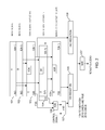
- FIG. 1 is a diagram illustrating implementation of zero detection of a sum of inputs without performing an addition, in accordance with a first embodiment of the present invention.
- Block 101 and 102 represent two vectors of a length N containing signed integer numbers in the 2's complement representation.
- Block 101 is a first vector of a length N containing signed integer numbers in the 2's complement representation—A(0:N ⁇ 1)
- block 102 is a second vector of a length N containing signed integer numbers in the 2's complement representation—B(0:N ⁇ 1).
- FIG. 5 illustrates an example of two input vectors ( 501 and 502 ) leading to a zero result, in accordance with one embodiment of the present invention.
- the invention takes advantage of the fact that the two input vectors must have a special structure if the result of their addition is zero.
- the two input vectors are either both zero or must be of different sign.
- the two input vectors must contain a series of ‘0’/‘1’ pairs followed by a ‘1’/‘1’ pair followed by ‘0’/‘0’ pairs.
- a bitwise XOR operation of the two input vectors (A(0:N ⁇ 1) and B(0:N ⁇ 1)) results in vector C.
- the bitwise XOR operation of the two input vectors (A(0:N ⁇ 1) and B(0:N ⁇ 1)) is implemented by one or more XOR gates in a circuit.
- a bitwise OR operation of the two input vectors (A(0:N ⁇ 1) and B(0:N ⁇ 1)) results in vector D.
- FIG. 6 is illustrates an example of the result of the bitwise XOR operation and the bitwise OR operation of vectors 501 and 502 , in accordance with one embodiment of the present invention.
- the bitwise XOR operation and the bitwise OR operation of the two input vectors with the special structure lead to vector 601 and vector 602 , respectively.
- Both vectors 601 and 602 contain ones in the most significant bits and zeros in the least significant bits.
- vector 602 (which is the result of the bitwise OR operation of vectors 501 and 502 ) contains a ‘1’ in this bit position and vector 601 (which is the result of the bitwise XOR operation of vectors 501 and 502 ) contains a ‘0’.
- vector 601 which is the result of the bitwise XOR operation of vectors 501 and 502 .
- bit positions of vector D are shifted by one bit to the left.
- the right end bit of vector D is padded by ‘0’.
- a bitwise XOR operation is operated for two vectors; the first vector is vector C from 0th bit to (N ⁇ 1)th bit, and the second vector is vector D from the 1st bit to (N ⁇ 1)th bit plus the padded ‘0’.
- the bitwise XOR operation of the two vectors is implemented by one or more XOR gates in a circuit. As shown by block 105 , the bitwise XOR operation results in vector E. E (0: N ⁇ 1): C (0 ,N ⁇ 1)XOR [ D (1 ,N ⁇ 1)& ‘0’]
- an XOR operation is performed for C′(0) and D(0).
- the XOR reduction is implemented by an XOR gate in a circuit.
- C′(0) is the sign extension of vector C.
- C′(0:N) C(0, 0:N ⁇ 1).
- bit positions of vector D are shifted by one bit to the left and the right end bit of vector D is padded by ‘0’.
- an AND operation is performed for the output of the XOR operation shown by block 106 and a control signal.
- the control signal switches between the first type of zero check and the second type of zero check. When the control signal is one, the true mathematical zero check (the first type of zero check) is enabled; when the control signal is zero, the true mathematical zero check is disabled.
- an OR reduction is performed for vector E and an output of the AND operation shown by block 107 .
- the OR reduction is implemented by an OR gate in a circuit.
- the OR reduction operates on all the bits of vector E and the output of the AND operation shown by block 107 , and the OR reduction returns a single-bit value. Then, the single-bit value is through an inverter as shown by block 110 .
- an AND reduction is performed for vector C.
- the AND reduction is implemented by an AND gate in a circuit.
- the AND reduction operates on all the bits of vector C and returns a single-bit value.
- the single-bit value is through an inverter as shown by block 111 .
- an AND operation is performed for an output of the inverter shown by block 110 and an output of the inverter shown by block 111 .
- the AND operation is implemented by an AND gate in a circuit. If both outputs of the inverters are 1, the output of the AND gate shown by block 112 will be 1; therefore, the sum of vectors A and B is a zero.
- the control signal enable the true mathematical zero check a true mathematical zero of the sum of vectors A and B is detected; when the control signal disable the true zero check, the trailing bits of the sum of vectors A and B are detected.
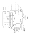
- FIG. 2 is a diagram illustrating implementation of zero detection of a sum of inputs without performing an addition, in accordance with a second embodiment of the present invention.
- the operations represented by blocks 101 , 102 , 103 , 104 , 105 , 106 , 107 , 108 , and 109 in FIG. 2 are the same as in FIG. 1 .
- the operations of these blocks have been discussed in previous paragraphs with reference to FIG. 1 .
- the OR reduction (block 108 ) operates on all the bits of vector E and the output of the AND operation shown by block 107 , and the OR operation returns a first single-bit value.
- the AND reduction (block 109 ) operates on all the bits of vector C and returns a second single-bit value.
- a NOR operation is performed for the first single-bit value and the second single-bit value.
- the NOR operation is implemented by an NOR gate in a circuit. If the output of the NOR gate shown by block 201 is 1, then the sum of vectors A and B is a zero.
- the control signal enable the true mathematical zero check a true mathematical zero of the sum of vectors A and B is detected; when the control signal disable the true zero check, the trailing bits of the sum of vectors A and B are detected.
- FIG. 3 is a diagram illustrating implementation of zero detection of a sum of inputs without performing an addition, in accordance with a third embodiment of the present invention.
- the operations represented by blocks 101 , 102 , 103 , 104 , 106 , 107 , and 109 in FIG. 3 are the same as in FIG. 1 .
- the operations of these blocks have been discussed in previous paragraphs with reference to FIG. 1 .
- a bitwise XNOR operation (block 301 ) is operated for two vectors; the first vector is vector C from 0th bit to (N ⁇ 1)th bit, and the second vector is vector D from the 1st bit to (N ⁇ 1)th bit plus the padded ‘0’.
- the bitwise XNOR operation of the two vectors is implemented by one or more XNOR gates in a circuit. As shown by block 301 , the bitwise XNOR operation results in vector E. E (0: N ⁇ 1): C (0, N ⁇ 1)XNOR [ D (1 ,N ⁇ 1)& ‘0’]
- an inverter shown by block 302 follows the AND operation shown by block 107 .
- an AND reduction is performed for vector E and an output of the inverter shown by block 302 .
- the AND reduction is implemented by an AND gate in a circuit.
- the AND reduction operates on all the bits of vector E and the output of the inverter shown by block 302 , and the AND reduction returns a single-bit value. Then, the single-bit value is an input of an AND operation performed by an AND gate shown by block 112 .
- the AND reduction shown by block 109 and the inverter shown by block 111 can be replaced by one or more inverters followed by an OR reduction.
- the one or more inverters invert vector C.
- FIG. 4 is a diagram illustrating implementation of zero detection of a sum of inputs without performing an addition, in accordance with a fourth embodiment of the present invention.
- the operations represented by blocks 101 , 102 , 103 , 104 , 105 , 106 , 107 , 108 , 110 , and 112 in FIG. 4 are the same as in FIG. 1 .
- the operations of these blocks have been discussed in previous paragraphs with reference to FIG. 1 .
- a NOT operation is performed for vector C.
- the NOT operation is implemented by one or more inverters shown by block 401 in a circuit.
- an OR reduction operates on all the bits of outputs of the one or more inverters shown by block 401 and returns a single-bit value.
- the OR reduction is implemented by an OR gate in a circuit.
- the single-bit value is an input of an AND operation performed by an AND gate shown by block 112 .
- the OR reduction operation shown by block 108 followed by the inverter shown by block 110 in FIG. 1 can be replaced by inverters followed by an AND reduction operation.
- the inverters include an inverter following the AND gate shown by block 107 and one or more inverters following the XOR operation shown by block 105 .
- the one or more inverters invert vector E.
- FIG. 7 is a diagram illustrating three corner cases of the structures of two input vectors which lead to a zero result, in accordance with one embodiment of the present invention.
- case 1 both input vectors 701 and 702 contain only zeros.
- case 2 both input vectors 703 and 704 contain a negative sign followed by all zeros.
- case 3 the ‘1’/‘1’ pair is in the least significant bit position of input vectors 705 and 706 . All the three corner cases are covered by the invention.
Landscapes
- Engineering & Computer Science (AREA)
- Theoretical Computer Science (AREA)
- Physics & Mathematics (AREA)
- General Physics & Mathematics (AREA)
- General Engineering & Computer Science (AREA)
- Computational Mathematics (AREA)
- Mathematical Analysis (AREA)
- Mathematical Optimization (AREA)
- Pure & Applied Mathematics (AREA)
- Computing Systems (AREA)
- Manipulation Of Pulses (AREA)
Abstract
Description
S(0: N)=A(0,0: N−1)+B(0,0: N−1)→zero=(S(0: N)==0)
An example of the first type is the zero check in the exponent calculation of floating-point units.
S(0: N−1)=A(0: N−1)+B(0: N−1)→zero=(S(0: N−1)==0)
The difference from the first type is that the sum is considered zero when its trailing N bits are zero. The overflowing case which maps to zero is A=B=10 . . . 0. This type of the zero check is used in the divide and square root algorithm.
C(0: N−1): A(0,N−1)XOR B(0,N−1)
The bitwise XOR operation of the two input vectors (A(0:N−1) and B(0:N−1)) is implemented by one or more XOR gates in a circuit. As shown by
D(0: N−1): A(0,N−1)OR B(0,N−1)
The bitwise OR operation of the two input vectors (A(0:N−1) and B(0:N−1)) is implemented by one or more OR gates in a circuit.
E(0: N−1): C(0,N−1)XOR [D(1,N−1)& ‘0’]
E(0: N−1): C(0,N−1)XNOR [D(1,N−1)& ‘0’]
Claims (13)
Priority Applications (1)
| Application Number | Priority Date | Filing Date | Title |
|---|---|---|---|
| US15/788,901 US10168993B2 (en) | 2017-02-22 | 2017-10-20 | Zero detection of a sum of inputs without performing an addition |
Applications Claiming Priority (2)
| Application Number | Priority Date | Filing Date | Title |
|---|---|---|---|
| US15/438,831 US10101967B2 (en) | 2017-02-22 | 2017-02-22 | Zero detection of a sum of inputs without performing an addition |
| US15/788,901 US10168993B2 (en) | 2017-02-22 | 2017-10-20 | Zero detection of a sum of inputs without performing an addition |
Related Parent Applications (1)
| Application Number | Title | Priority Date | Filing Date |
|---|---|---|---|
| US15/438,831 Continuation US10101967B2 (en) | 2017-02-22 | 2017-02-22 | Zero detection of a sum of inputs without performing an addition |
Publications (2)
| Publication Number | Publication Date |
|---|---|
| US20180239589A1 US20180239589A1 (en) | 2018-08-23 |
| US10168993B2 true US10168993B2 (en) | 2019-01-01 |
Family
ID=63167780
Family Applications (2)
| Application Number | Title | Priority Date | Filing Date |
|---|---|---|---|
| US15/438,831 Active US10101967B2 (en) | 2017-02-22 | 2017-02-22 | Zero detection of a sum of inputs without performing an addition |
| US15/788,901 Expired - Fee Related US10168993B2 (en) | 2017-02-22 | 2017-10-20 | Zero detection of a sum of inputs without performing an addition |
Family Applications Before (1)
| Application Number | Title | Priority Date | Filing Date |
|---|---|---|---|
| US15/438,831 Active US10101967B2 (en) | 2017-02-22 | 2017-02-22 | Zero detection of a sum of inputs without performing an addition |
Country Status (1)
| Country | Link |
|---|---|
| US (2) | US10101967B2 (en) |
Families Citing this family (2)
| Publication number | Priority date | Publication date | Assignee | Title |
|---|---|---|---|---|
| US11488002B2 (en) * | 2018-02-15 | 2022-11-01 | Atlazo, Inc. | Binary neural network accelerator engine methods and systems |
| US11188316B2 (en) * | 2020-03-09 | 2021-11-30 | International Business Machines Corporation | Performance optimization of class instance comparisons |
Citations (9)
| Publication number | Priority date | Publication date | Assignee | Title |
|---|---|---|---|---|
| US5020016A (en) | 1988-04-29 | 1991-05-28 | Nec Corporation | Circuit for detecting zero result of addition/subtraction by simultaneously processing each pair of corresponding bits of a pair of given numbers in parralel |
| US5367477A (en) | 1993-11-29 | 1994-11-22 | Motorola, Inc. | Method and apparatus for performing parallel zero detection in a data processing system |
| US5581496A (en) | 1992-07-20 | 1996-12-03 | Industrial Technology Research Institute | Zero-flag generator for adder |
| US5798958A (en) | 1996-06-05 | 1998-08-25 | Samsung Electronics Co., Ltd. | Zero detect for binary sum |
| US6424955B1 (en) | 1998-06-10 | 2002-07-23 | Lsi Logic Corporation | Zero detection in digital processing |
| US8015230B2 (en) | 2007-06-08 | 2011-09-06 | Apple Inc. | Fast modular zero sum and ones sum determination |
| US20130262546A1 (en) | 2012-03-30 | 2013-10-03 | Fujitsu Limited | Arithmetic circuit and arithmetic method |
| US8578196B2 (en) | 2008-07-18 | 2013-11-05 | International Business Machines Corporation | Zero indication forwarding for floating point unit power reduction |
| US20140351308A1 (en) | 2013-05-23 | 2014-11-27 | Nvidia Corporation | System and method for dynamically reducing power consumption of floating-point logic |
-
2017
- 2017-02-22 US US15/438,831 patent/US10101967B2/en active Active
- 2017-10-20 US US15/788,901 patent/US10168993B2/en not_active Expired - Fee Related
Patent Citations (9)
| Publication number | Priority date | Publication date | Assignee | Title |
|---|---|---|---|---|
| US5020016A (en) | 1988-04-29 | 1991-05-28 | Nec Corporation | Circuit for detecting zero result of addition/subtraction by simultaneously processing each pair of corresponding bits of a pair of given numbers in parralel |
| US5581496A (en) | 1992-07-20 | 1996-12-03 | Industrial Technology Research Institute | Zero-flag generator for adder |
| US5367477A (en) | 1993-11-29 | 1994-11-22 | Motorola, Inc. | Method and apparatus for performing parallel zero detection in a data processing system |
| US5798958A (en) | 1996-06-05 | 1998-08-25 | Samsung Electronics Co., Ltd. | Zero detect for binary sum |
| US6424955B1 (en) | 1998-06-10 | 2002-07-23 | Lsi Logic Corporation | Zero detection in digital processing |
| US8015230B2 (en) | 2007-06-08 | 2011-09-06 | Apple Inc. | Fast modular zero sum and ones sum determination |
| US8578196B2 (en) | 2008-07-18 | 2013-11-05 | International Business Machines Corporation | Zero indication forwarding for floating point unit power reduction |
| US20130262546A1 (en) | 2012-03-30 | 2013-10-03 | Fujitsu Limited | Arithmetic circuit and arithmetic method |
| US20140351308A1 (en) | 2013-05-23 | 2014-11-27 | Nvidia Corporation | System and method for dynamically reducing power consumption of floating-point logic |
Non-Patent Citations (4)
| Title |
|---|
| Appendix P List of IBM Patents or Applications Treated as Related Dated Oct. 20, 2017. Two pages. |
| Kroener et al. Original U.S. Appl. No. 15/438,831, filed Feb. 22, 2017 as DE920160108US1. |
| Lutz et al., "Early Zero Detection ," 1996 IEEE International Conference on Computer Design: VLSI in Computers and Processors, Oct. 7-9, 1996, ©1996 IEEE, pp. 545-550. |
| Weinberger, Arnold, "High-Speed Zero-Sum Detection," Proceedings of the 3rd IEEE Symposium on Computer Arithmetic, Southern Methodist University, Dallas, Texas, Nov. 19-20, 1975, pp. 200-207. |
Also Published As
| Publication number | Publication date |
|---|---|
| US10101967B2 (en) | 2018-10-16 |
| US20180239589A1 (en) | 2018-08-23 |
| US20180239588A1 (en) | 2018-08-23 |
Similar Documents
| Publication | Publication Date | Title |
|---|---|---|
| US9483232B2 (en) | Data processing apparatus and method for multiplying floating point operands | |
| US5010508A (en) | Prenormalization for a floating-point adder | |
| Tao et al. | Three-operand floating-point adder | |
| JP4500358B2 (en) | Arithmetic processing apparatus and arithmetic processing method | |
| US8185570B2 (en) | Three-term input floating-point adder-subtractor | |
| US9122517B2 (en) | Fused multiply-adder with booth-encoding | |
| US7668892B2 (en) | Data processing apparatus and method for normalizing a data value | |
| CN108694037B (en) | Apparatus and method for estimating shift amount when floating point subtraction is performed | |
| US10338889B2 (en) | Apparatus and method for controlling rounding when performing a floating point operation | |
| US10168993B2 (en) | Zero detection of a sum of inputs without performing an addition | |
| KR102412746B1 (en) | Apparatus and method for performing floating-point square root operation | |
| US7437400B2 (en) | Data processing apparatus and method for performing floating point addition | |
| US9430190B2 (en) | Fused multiply add pipeline | |
| US11762633B2 (en) | Circuit and method for binary flag determination | |
| US20050114422A1 (en) | High performance implementation of exponent adjustment in a floating point design | |
| JPH02294731A (en) | Floating point arithmetic processor | |
| KR102459011B1 (en) | Leading zero anticipation | |
| Mathis et al. | A novel single/double precision normalized IEEE 754 floating-point adder/subtracter | |
| US8250126B2 (en) | Efficient leading zero anticipator | |
| US7356553B2 (en) | Data processing apparatus and method for determining a processing path to perform a data processing operation on input data elements | |
| US6571264B1 (en) | Floating-point arithmetic device | |
| Rahman et al. | Optimized hardware architecture for implementing IEEE 754 standard double precision floating point adder/subtractor | |
| US6963896B2 (en) | Method and system to implement an improved floating point adder with integrated adding and rounding | |
| US10275218B1 (en) | Apparatus and method for subtracting significand values of floating-point operands | |
| US7051062B2 (en) | Apparatus and method for adding multiple-bit binary-strings |
Legal Events
| Date | Code | Title | Description |
|---|---|---|---|
| AS | Assignment |
Owner name: INTERNATIONAL BUSINESS MACHINES CORPORATION, NEW Y Free format text: ASSIGNMENT OF ASSIGNORS INTEREST;ASSIGNORS:KROENER, MICHAEL K.;MUELLER, SILVIA M., DR.;NIEKISCH, MANUELA;AND OTHERS;REEL/FRAME:043909/0862 Effective date: 20170221 |
|
| FEPP | Fee payment procedure |
Free format text: ENTITY STATUS SET TO UNDISCOUNTED (ORIGINAL EVENT CODE: BIG.); ENTITY STATUS OF PATENT OWNER: LARGE ENTITY |
|
| STCF | Information on status: patent grant |
Free format text: PATENTED CASE |
|
| FEPP | Fee payment procedure |
Free format text: MAINTENANCE FEE REMINDER MAILED (ORIGINAL EVENT CODE: REM.); ENTITY STATUS OF PATENT OWNER: LARGE ENTITY |
|
| LAPS | Lapse for failure to pay maintenance fees |
Free format text: PATENT EXPIRED FOR FAILURE TO PAY MAINTENANCE FEES (ORIGINAL EVENT CODE: EXP.); ENTITY STATUS OF PATENT OWNER: LARGE ENTITY |
|
| STCH | Information on status: patent discontinuation |
Free format text: PATENT EXPIRED DUE TO NONPAYMENT OF MAINTENANCE FEES UNDER 37 CFR 1.362 |
|
| FP | Lapsed due to failure to pay maintenance fee |
Effective date: 20230101 |