US10152159B2 - Display panel and method for forming an array substrate of a display panel - Google Patents
Display panel and method for forming an array substrate of a display panel Download PDFInfo
- Publication number
- US10152159B2 US10152159B2 US15/620,680 US201715620680A US10152159B2 US 10152159 B2 US10152159 B2 US 10152159B2 US 201715620680 A US201715620680 A US 201715620680A US 10152159 B2 US10152159 B2 US 10152159B2
- Authority
- US
- United States
- Prior art keywords
- layer
- conductive layer
- drain
- gate
- source
- Prior art date
- Legal status (The legal status is an assumption and is not a legal conclusion. Google has not performed a legal analysis and makes no representation as to the accuracy of the status listed.)
- Active, expires
Links
- 239000000758 substrate Substances 0.000 title claims abstract description 131
- 238000000034 method Methods 0.000 title description 67
- 239000010410 layer Substances 0.000 claims abstract description 1041
- 230000008054 signal transmission Effects 0.000 claims abstract description 66
- 239000010409 thin film Substances 0.000 claims abstract description 27
- 239000002356 single layer Substances 0.000 claims abstract description 15
- 230000008569 process Effects 0.000 description 46
- 239000004065 semiconductor Substances 0.000 description 34
- 239000002184 metal Substances 0.000 description 28
- 238000010586 diagram Methods 0.000 description 19
- 238000005530 etching Methods 0.000 description 10
- 238000004519 manufacturing process Methods 0.000 description 9
- 239000000463 material Substances 0.000 description 8
- 230000015572 biosynthetic process Effects 0.000 description 6
- 229910021420 polycrystalline silicon Inorganic materials 0.000 description 5
- 238000005516 engineering process Methods 0.000 description 4
- 239000004973 liquid crystal related substance Substances 0.000 description 4
- XUIMIQQOPSSXEZ-UHFFFAOYSA-N Silicon Chemical compound [Si] XUIMIQQOPSSXEZ-UHFFFAOYSA-N 0.000 description 3
- 229910052710 silicon Inorganic materials 0.000 description 3
- 239000010703 silicon Substances 0.000 description 3
- 230000008878 coupling Effects 0.000 description 2
- 238000010168 coupling process Methods 0.000 description 2
- 238000005859 coupling reaction Methods 0.000 description 2
- 230000003247 decreasing effect Effects 0.000 description 2
- 238000009826 distribution Methods 0.000 description 2
- 239000010408 film Substances 0.000 description 2
- 230000035945 sensitivity Effects 0.000 description 2
- 230000004888 barrier function Effects 0.000 description 1
- 239000003990 capacitor Substances 0.000 description 1
- 238000011161 development Methods 0.000 description 1
- 230000005684 electric field Effects 0.000 description 1
- 238000005468 ion implantation Methods 0.000 description 1
- 239000007769 metal material Substances 0.000 description 1
- 238000012986 modification Methods 0.000 description 1
- 230000004048 modification Effects 0.000 description 1
- 238000004806 packaging method and process Methods 0.000 description 1
- 238000012545 processing Methods 0.000 description 1
- 230000000750 progressive effect Effects 0.000 description 1
Images


Classifications
-
- G—PHYSICS
- G06—COMPUTING; CALCULATING OR COUNTING
- G06F—ELECTRIC DIGITAL DATA PROCESSING
- G06F3/00—Input arrangements for transferring data to be processed into a form capable of being handled by the computer; Output arrangements for transferring data from processing unit to output unit, e.g. interface arrangements
- G06F3/01—Input arrangements or combined input and output arrangements for interaction between user and computer
- G06F3/03—Arrangements for converting the position or the displacement of a member into a coded form
- G06F3/041—Digitisers, e.g. for touch screens or touch pads, characterised by the transducing means
- G06F3/0412—Digitisers structurally integrated in a display
-
- G—PHYSICS
- G02—OPTICS
- G02F—OPTICAL DEVICES OR ARRANGEMENTS FOR THE CONTROL OF LIGHT BY MODIFICATION OF THE OPTICAL PROPERTIES OF THE MEDIA OF THE ELEMENTS INVOLVED THEREIN; NON-LINEAR OPTICS; FREQUENCY-CHANGING OF LIGHT; OPTICAL LOGIC ELEMENTS; OPTICAL ANALOGUE/DIGITAL CONVERTERS
- G02F1/00—Devices or arrangements for the control of the intensity, colour, phase, polarisation or direction of light arriving from an independent light source, e.g. switching, gating or modulating; Non-linear optics
- G02F1/01—Devices or arrangements for the control of the intensity, colour, phase, polarisation or direction of light arriving from an independent light source, e.g. switching, gating or modulating; Non-linear optics for the control of the intensity, phase, polarisation or colour
- G02F1/13—Devices or arrangements for the control of the intensity, colour, phase, polarisation or direction of light arriving from an independent light source, e.g. switching, gating or modulating; Non-linear optics for the control of the intensity, phase, polarisation or colour based on liquid crystals, e.g. single liquid crystal display cells
- G02F1/133—Constructional arrangements; Operation of liquid crystal cells; Circuit arrangements
- G02F1/1333—Constructional arrangements; Manufacturing methods
- G02F1/13338—Input devices, e.g. touch panels
-
- G—PHYSICS
- G06—COMPUTING; CALCULATING OR COUNTING
- G06F—ELECTRIC DIGITAL DATA PROCESSING
- G06F3/00—Input arrangements for transferring data to be processed into a form capable of being handled by the computer; Output arrangements for transferring data from processing unit to output unit, e.g. interface arrangements
- G06F3/01—Input arrangements or combined input and output arrangements for interaction between user and computer
- G06F3/03—Arrangements for converting the position or the displacement of a member into a coded form
- G06F3/041—Digitisers, e.g. for touch screens or touch pads, characterised by the transducing means
- G06F3/044—Digitisers, e.g. for touch screens or touch pads, characterised by the transducing means by capacitive means
- G06F3/0445—Digitisers, e.g. for touch screens or touch pads, characterised by the transducing means by capacitive means using two or more layers of sensing electrodes, e.g. using two layers of electrodes separated by a dielectric layer
-
- G—PHYSICS
- G06—COMPUTING; CALCULATING OR COUNTING
- G06F—ELECTRIC DIGITAL DATA PROCESSING
- G06F3/00—Input arrangements for transferring data to be processed into a form capable of being handled by the computer; Output arrangements for transferring data from processing unit to output unit, e.g. interface arrangements
- G06F3/01—Input arrangements or combined input and output arrangements for interaction between user and computer
- G06F3/03—Arrangements for converting the position or the displacement of a member into a coded form
- G06F3/041—Digitisers, e.g. for touch screens or touch pads, characterised by the transducing means
- G06F3/044—Digitisers, e.g. for touch screens or touch pads, characterised by the transducing means by capacitive means
- G06F3/0446—Digitisers, e.g. for touch screens or touch pads, characterised by the transducing means by capacitive means using a grid-like structure of electrodes in at least two directions, e.g. using row and column electrodes
-
- G—PHYSICS
- G06—COMPUTING; CALCULATING OR COUNTING
- G06F—ELECTRIC DIGITAL DATA PROCESSING
- G06F3/00—Input arrangements for transferring data to be processed into a form capable of being handled by the computer; Output arrangements for transferring data from processing unit to output unit, e.g. interface arrangements
- G06F3/01—Input arrangements or combined input and output arrangements for interaction between user and computer
- G06F3/03—Arrangements for converting the position or the displacement of a member into a coded form
- G06F3/041—Digitisers, e.g. for touch screens or touch pads, characterised by the transducing means
- G06F3/044—Digitisers, e.g. for touch screens or touch pads, characterised by the transducing means by capacitive means
- G06F3/0447—Position sensing using the local deformation of sensor cells
-
- G—PHYSICS
- G09—EDUCATION; CRYPTOGRAPHY; DISPLAY; ADVERTISING; SEALS
- G09G—ARRANGEMENTS OR CIRCUITS FOR CONTROL OF INDICATING DEVICES USING STATIC MEANS TO PRESENT VARIABLE INFORMATION
- G09G3/00—Control arrangements or circuits, of interest only in connection with visual indicators other than cathode-ray tubes
- G09G3/20—Control arrangements or circuits, of interest only in connection with visual indicators other than cathode-ray tubes for presentation of an assembly of a number of characters, e.g. a page, by composing the assembly by combination of individual elements arranged in a matrix no fixed position being assigned to or needed to be assigned to the individual characters or partial characters
- G09G3/34—Control arrangements or circuits, of interest only in connection with visual indicators other than cathode-ray tubes for presentation of an assembly of a number of characters, e.g. a page, by composing the assembly by combination of individual elements arranged in a matrix no fixed position being assigned to or needed to be assigned to the individual characters or partial characters by control of light from an independent source
- G09G3/36—Control arrangements or circuits, of interest only in connection with visual indicators other than cathode-ray tubes for presentation of an assembly of a number of characters, e.g. a page, by composing the assembly by combination of individual elements arranged in a matrix no fixed position being assigned to or needed to be assigned to the individual characters or partial characters by control of light from an independent source using liquid crystals
- G09G3/3611—Control of matrices with row and column drivers
- G09G3/3674—Details of drivers for scan electrodes
- G09G3/3677—Details of drivers for scan electrodes suitable for active matrices only
-
- H—ELECTRICITY
- H01—ELECTRIC ELEMENTS
- H01L—SEMICONDUCTOR DEVICES NOT COVERED BY CLASS H10
- H01L27/00—Devices consisting of a plurality of semiconductor or other solid-state components formed in or on a common substrate
- H01L27/02—Devices consisting of a plurality of semiconductor or other solid-state components formed in or on a common substrate including semiconductor components specially adapted for rectifying, oscillating, amplifying or switching and having potential barriers; including integrated passive circuit elements having potential barriers
- H01L27/12—Devices consisting of a plurality of semiconductor or other solid-state components formed in or on a common substrate including semiconductor components specially adapted for rectifying, oscillating, amplifying or switching and having potential barriers; including integrated passive circuit elements having potential barriers the substrate being other than a semiconductor body, e.g. an insulating body
- H01L27/1214—Devices consisting of a plurality of semiconductor or other solid-state components formed in or on a common substrate including semiconductor components specially adapted for rectifying, oscillating, amplifying or switching and having potential barriers; including integrated passive circuit elements having potential barriers the substrate being other than a semiconductor body, e.g. an insulating body comprising a plurality of TFTs formed on a non-semiconducting substrate, e.g. driving circuits for AMLCDs
- H01L27/124—Devices consisting of a plurality of semiconductor or other solid-state components formed in or on a common substrate including semiconductor components specially adapted for rectifying, oscillating, amplifying or switching and having potential barriers; including integrated passive circuit elements having potential barriers the substrate being other than a semiconductor body, e.g. an insulating body comprising a plurality of TFTs formed on a non-semiconducting substrate, e.g. driving circuits for AMLCDs with a particular composition, shape or layout of the wiring layers specially adapted to the circuit arrangement, e.g. scanning lines in LCD pixel circuits
-
- H—ELECTRICITY
- H01—ELECTRIC ELEMENTS
- H01L—SEMICONDUCTOR DEVICES NOT COVERED BY CLASS H10
- H01L27/00—Devices consisting of a plurality of semiconductor or other solid-state components formed in or on a common substrate
- H01L27/02—Devices consisting of a plurality of semiconductor or other solid-state components formed in or on a common substrate including semiconductor components specially adapted for rectifying, oscillating, amplifying or switching and having potential barriers; including integrated passive circuit elements having potential barriers
- H01L27/12—Devices consisting of a plurality of semiconductor or other solid-state components formed in or on a common substrate including semiconductor components specially adapted for rectifying, oscillating, amplifying or switching and having potential barriers; including integrated passive circuit elements having potential barriers the substrate being other than a semiconductor body, e.g. an insulating body
- H01L27/1214—Devices consisting of a plurality of semiconductor or other solid-state components formed in or on a common substrate including semiconductor components specially adapted for rectifying, oscillating, amplifying or switching and having potential barriers; including integrated passive circuit elements having potential barriers the substrate being other than a semiconductor body, e.g. an insulating body comprising a plurality of TFTs formed on a non-semiconducting substrate, e.g. driving circuits for AMLCDs
- H01L27/1259—Multistep manufacturing methods
-
- H—ELECTRICITY
- H01—ELECTRIC ELEMENTS
- H01L—SEMICONDUCTOR DEVICES NOT COVERED BY CLASS H10
- H01L33/00—Semiconductor devices having potential barriers specially adapted for light emission; Processes or apparatus specially adapted for the manufacture or treatment thereof or of parts thereof; Details thereof
- H01L33/36—Semiconductor devices having potential barriers specially adapted for light emission; Processes or apparatus specially adapted for the manufacture or treatment thereof or of parts thereof; Details thereof characterised by the electrodes
-
- H01L51/5203—
-
- H—ELECTRICITY
- H05—ELECTRIC TECHNIQUES NOT OTHERWISE PROVIDED FOR
- H05K—PRINTED CIRCUITS; CASINGS OR CONSTRUCTIONAL DETAILS OF ELECTRIC APPARATUS; MANUFACTURE OF ASSEMBLAGES OF ELECTRICAL COMPONENTS
- H05K1/00—Printed circuits
- H05K1/02—Details
- H05K1/0296—Conductive pattern lay-out details not covered by sub groups H05K1/02 - H05K1/0295
- H05K1/0298—Multilayer circuits
-
- H—ELECTRICITY
- H10—SEMICONDUCTOR DEVICES; ELECTRIC SOLID-STATE DEVICES NOT OTHERWISE PROVIDED FOR
- H10K—ORGANIC ELECTRIC SOLID-STATE DEVICES
- H10K50/00—Organic light-emitting devices
- H10K50/80—Constructional details
- H10K50/805—Electrodes
-
- G—PHYSICS
- G02—OPTICS
- G02F—OPTICAL DEVICES OR ARRANGEMENTS FOR THE CONTROL OF LIGHT BY MODIFICATION OF THE OPTICAL PROPERTIES OF THE MEDIA OF THE ELEMENTS INVOLVED THEREIN; NON-LINEAR OPTICS; FREQUENCY-CHANGING OF LIGHT; OPTICAL LOGIC ELEMENTS; OPTICAL ANALOGUE/DIGITAL CONVERTERS
- G02F1/00—Devices or arrangements for the control of the intensity, colour, phase, polarisation or direction of light arriving from an independent light source, e.g. switching, gating or modulating; Non-linear optics
- G02F1/01—Devices or arrangements for the control of the intensity, colour, phase, polarisation or direction of light arriving from an independent light source, e.g. switching, gating or modulating; Non-linear optics for the control of the intensity, phase, polarisation or colour
- G02F1/13—Devices or arrangements for the control of the intensity, colour, phase, polarisation or direction of light arriving from an independent light source, e.g. switching, gating or modulating; Non-linear optics for the control of the intensity, phase, polarisation or colour based on liquid crystals, e.g. single liquid crystal display cells
- G02F1/133—Constructional arrangements; Operation of liquid crystal cells; Circuit arrangements
- G02F1/1333—Constructional arrangements; Manufacturing methods
- G02F1/133345—Insulating layers
-
- G—PHYSICS
- G02—OPTICS
- G02F—OPTICAL DEVICES OR ARRANGEMENTS FOR THE CONTROL OF LIGHT BY MODIFICATION OF THE OPTICAL PROPERTIES OF THE MEDIA OF THE ELEMENTS INVOLVED THEREIN; NON-LINEAR OPTICS; FREQUENCY-CHANGING OF LIGHT; OPTICAL LOGIC ELEMENTS; OPTICAL ANALOGUE/DIGITAL CONVERTERS
- G02F1/00—Devices or arrangements for the control of the intensity, colour, phase, polarisation or direction of light arriving from an independent light source, e.g. switching, gating or modulating; Non-linear optics
- G02F1/01—Devices or arrangements for the control of the intensity, colour, phase, polarisation or direction of light arriving from an independent light source, e.g. switching, gating or modulating; Non-linear optics for the control of the intensity, phase, polarisation or colour
- G02F1/13—Devices or arrangements for the control of the intensity, colour, phase, polarisation or direction of light arriving from an independent light source, e.g. switching, gating or modulating; Non-linear optics for the control of the intensity, phase, polarisation or colour based on liquid crystals, e.g. single liquid crystal display cells
- G02F1/133—Constructional arrangements; Operation of liquid crystal cells; Circuit arrangements
- G02F1/1333—Constructional arrangements; Manufacturing methods
- G02F1/1343—Electrodes
- G02F1/134309—Electrodes characterised by their geometrical arrangement
-
- G—PHYSICS
- G02—OPTICS
- G02F—OPTICAL DEVICES OR ARRANGEMENTS FOR THE CONTROL OF LIGHT BY MODIFICATION OF THE OPTICAL PROPERTIES OF THE MEDIA OF THE ELEMENTS INVOLVED THEREIN; NON-LINEAR OPTICS; FREQUENCY-CHANGING OF LIGHT; OPTICAL LOGIC ELEMENTS; OPTICAL ANALOGUE/DIGITAL CONVERTERS
- G02F1/00—Devices or arrangements for the control of the intensity, colour, phase, polarisation or direction of light arriving from an independent light source, e.g. switching, gating or modulating; Non-linear optics
- G02F1/01—Devices or arrangements for the control of the intensity, colour, phase, polarisation or direction of light arriving from an independent light source, e.g. switching, gating or modulating; Non-linear optics for the control of the intensity, phase, polarisation or colour
- G02F1/13—Devices or arrangements for the control of the intensity, colour, phase, polarisation or direction of light arriving from an independent light source, e.g. switching, gating or modulating; Non-linear optics for the control of the intensity, phase, polarisation or colour based on liquid crystals, e.g. single liquid crystal display cells
- G02F1/133—Constructional arrangements; Operation of liquid crystal cells; Circuit arrangements
- G02F1/1333—Constructional arrangements; Manufacturing methods
- G02F1/1343—Electrodes
- G02F1/13439—Electrodes characterised by their electrical, optical, physical properties; materials therefor; method of making
-
- G—PHYSICS
- G02—OPTICS
- G02F—OPTICAL DEVICES OR ARRANGEMENTS FOR THE CONTROL OF LIGHT BY MODIFICATION OF THE OPTICAL PROPERTIES OF THE MEDIA OF THE ELEMENTS INVOLVED THEREIN; NON-LINEAR OPTICS; FREQUENCY-CHANGING OF LIGHT; OPTICAL LOGIC ELEMENTS; OPTICAL ANALOGUE/DIGITAL CONVERTERS
- G02F1/00—Devices or arrangements for the control of the intensity, colour, phase, polarisation or direction of light arriving from an independent light source, e.g. switching, gating or modulating; Non-linear optics
- G02F1/01—Devices or arrangements for the control of the intensity, colour, phase, polarisation or direction of light arriving from an independent light source, e.g. switching, gating or modulating; Non-linear optics for the control of the intensity, phase, polarisation or colour
- G02F1/13—Devices or arrangements for the control of the intensity, colour, phase, polarisation or direction of light arriving from an independent light source, e.g. switching, gating or modulating; Non-linear optics for the control of the intensity, phase, polarisation or colour based on liquid crystals, e.g. single liquid crystal display cells
- G02F1/133—Constructional arrangements; Operation of liquid crystal cells; Circuit arrangements
- G02F1/136—Liquid crystal cells structurally associated with a semi-conducting layer or substrate, e.g. cells forming part of an integrated circuit
- G02F1/1362—Active matrix addressed cells
- G02F1/136286—Wiring, e.g. gate line, drain line
- G02F1/136295—Materials; Compositions; Manufacture processes
-
- G—PHYSICS
- G02—OPTICS
- G02F—OPTICAL DEVICES OR ARRANGEMENTS FOR THE CONTROL OF LIGHT BY MODIFICATION OF THE OPTICAL PROPERTIES OF THE MEDIA OF THE ELEMENTS INVOLVED THEREIN; NON-LINEAR OPTICS; FREQUENCY-CHANGING OF LIGHT; OPTICAL LOGIC ELEMENTS; OPTICAL ANALOGUE/DIGITAL CONVERTERS
- G02F1/00—Devices or arrangements for the control of the intensity, colour, phase, polarisation or direction of light arriving from an independent light source, e.g. switching, gating or modulating; Non-linear optics
- G02F1/01—Devices or arrangements for the control of the intensity, colour, phase, polarisation or direction of light arriving from an independent light source, e.g. switching, gating or modulating; Non-linear optics for the control of the intensity, phase, polarisation or colour
- G02F1/13—Devices or arrangements for the control of the intensity, colour, phase, polarisation or direction of light arriving from an independent light source, e.g. switching, gating or modulating; Non-linear optics for the control of the intensity, phase, polarisation or colour based on liquid crystals, e.g. single liquid crystal display cells
- G02F1/133—Constructional arrangements; Operation of liquid crystal cells; Circuit arrangements
- G02F1/136—Liquid crystal cells structurally associated with a semi-conducting layer or substrate, e.g. cells forming part of an integrated circuit
- G02F1/1362—Active matrix addressed cells
- G02F1/1368—Active matrix addressed cells in which the switching element is a three-electrode device
-
- G02F2001/136295—
-
- G—PHYSICS
- G02—OPTICS
- G02F—OPTICAL DEVICES OR ARRANGEMENTS FOR THE CONTROL OF LIGHT BY MODIFICATION OF THE OPTICAL PROPERTIES OF THE MEDIA OF THE ELEMENTS INVOLVED THEREIN; NON-LINEAR OPTICS; FREQUENCY-CHANGING OF LIGHT; OPTICAL LOGIC ELEMENTS; OPTICAL ANALOGUE/DIGITAL CONVERTERS
- G02F2201/00—Constructional arrangements not provided for in groups G02F1/00 - G02F7/00
- G02F2201/12—Constructional arrangements not provided for in groups G02F1/00 - G02F7/00 electrode
- G02F2201/121—Constructional arrangements not provided for in groups G02F1/00 - G02F7/00 electrode common or background
-
- G—PHYSICS
- G02—OPTICS
- G02F—OPTICAL DEVICES OR ARRANGEMENTS FOR THE CONTROL OF LIGHT BY MODIFICATION OF THE OPTICAL PROPERTIES OF THE MEDIA OF THE ELEMENTS INVOLVED THEREIN; NON-LINEAR OPTICS; FREQUENCY-CHANGING OF LIGHT; OPTICAL LOGIC ELEMENTS; OPTICAL ANALOGUE/DIGITAL CONVERTERS
- G02F2201/00—Constructional arrangements not provided for in groups G02F1/00 - G02F7/00
- G02F2201/12—Constructional arrangements not provided for in groups G02F1/00 - G02F7/00 electrode
- G02F2201/123—Constructional arrangements not provided for in groups G02F1/00 - G02F7/00 electrode pixel
-
- G—PHYSICS
- G06—COMPUTING; CALCULATING OR COUNTING
- G06F—ELECTRIC DIGITAL DATA PROCESSING
- G06F2203/00—Indexing scheme relating to G06F3/00 - G06F3/048
- G06F2203/041—Indexing scheme relating to G06F3/041 - G06F3/045
- G06F2203/04105—Pressure sensors for measuring the pressure or force exerted on the touch surface without providing the touch position
-
- G—PHYSICS
- G09—EDUCATION; CRYPTOGRAPHY; DISPLAY; ADVERTISING; SEALS
- G09G—ARRANGEMENTS OR CIRCUITS FOR CONTROL OF INDICATING DEVICES USING STATIC MEANS TO PRESENT VARIABLE INFORMATION
- G09G2300/00—Aspects of the constitution of display devices
- G09G2300/04—Structural and physical details of display devices
- G09G2300/0421—Structural details of the set of electrodes
- G09G2300/0426—Layout of electrodes and connections
Definitions
- the present application generally relates to display technology, and more particularly, to a display panel and a method for forming an array substrate of a display panel.
- a display panel may include a display region and a frame region. Gates, sources, drains, common electrodes and pixel electrodes may be disposed in the display region, while drive circuits and wires are arranged in the frame region.
- the wires are used for coupling the drive circuits with the components in the display region.
- the width of the frame region is mainly depended on the width of a region for placing these wires.
- a display panel needs to accommodate more pixel electrodes.
- the number of wires for connecting the pixel electrodes also increases, which refers to the width of the frame region is not likely to decrease.
- the present disclosure provides a display panel and a method for forming an array substrate of a display panel.
- the array substrate may have a frame region with a smaller size.
- a display panel including an array substrate includes a display region and a frame region.
- the frame region includes a drive circuit region and a wire region.
- Wires formed in the wire region are configured to electrically connect components in the drive circuit region to components in the display region.
- In the wire region there are formed a plurality of first signal wires each of which includes a first conductive layer stacked with a second conductive layer.
- a first insulating layer is disposed between the first and the second conductive layers.
- One layer stacked with another layer refers to that the two layers are at least partially overlapped with each other in a direction perpendicular to the array substrate.
- more than two layers stacked with each other refers to that each layer is at least partially overlapped with at least another one of the layers in the direction perpendicular to the array substrate.
- a method for forming an array substrate of a display panel includes: providing a first substrate; forming a first conductive layer in a first signal wire region of a wire region, where the wire region is disposed on a first surface of the first substrate; forming a first insulating layer overlaying the first conductive layer; forming a first via in the first insulating layer, where the first via is in contact with the first conductive layer; and forming a second conductive layer on the first insulating layer, where the first and the second conductive layers are electrically connected through the first via.
- a display panel includes the above array substrate.
- a display panel includes an array substrate.
- the array substrate includes a display region and a frame region.
- the display region includes a signal transmission wire layer.
- the frame region includes a gate circuit drive unit.
- the gate circuit drive unit includes a thin film transistor, and the thin film transistor includes a source, a drain and a gate.
- the frame region further includes a driving circuit and a first signal lead line.
- the first signal lead line is arranged on a single layer and arranged on a same layer as the signal transmission wire layer of the display region. One end of the first signal lead line is electrically connected to the gate, and the other end of the first signal lead line is electrically connected to the driving circuit.
- a touch control display device includes the above touch panel.
- FIG. 1 is a top view of an array substrate according to an embodiment of the present disclosure
- FIG. 2 is a cross section of a first signal wire in an array substrate according to another embodiment of the present disclosure
- FIG. 3 illustrates how a first signal wire is electrically connected with a third signal wire according to another embodiment of the present disclosure
- FIG. 4 is a cross section of a display region in an array substrate according to another embodiment of the present disclosure.
- FIGS. 5 to 9 are cross sections of array substrates according to another embodiment of the present disclosure.
- FIG. 10 is a cross section of a second signal wire according to another embodiment of the present disclosure.
- FIGS. 11 to 20 are cross sections of array substrates according to another embodiment of the present disclosure.
- FIG. 21 is a flow chart of a process for forming an array substrate according to another embodiment of the present disclosure.
- FIG. 22 is a flow chart of another process for forming an array substrate according to another embodiment of the present disclosure.
- FIGS. 23 to 26 are cross sections of wire regions in array substrates according to another embodiment of the present disclosure.
- FIGS. 27 to 36 are cross sections of array substrates according to another embodiment of the present disclosure.
- FIG. 37 is a cross section of a display panel according to another embodiment of the present disclosure.
- FIG. 38 is a schematic diagram of a display panel integrated with a touch control function according to an embodiment of the present disclosure.
- FIG. 39 is a schematic diagram of a touch control structure in a mutual capacitance manner according to an embodiment of the present disclosure.
- FIG. 40 is a cross-sectional view of a touch control structure in a mutual capacitance manner along the CD line as shown in FIG. 39 according to an embodiment of the present disclosure
- FIG. 41 is a cross-sectional view of a touch control structure in a mutual capacitance manner along the CD line as shown in FIG. 39 according to an embodiment of the present disclosure
- FIG. 42 is a cross-sectional view of a touch control structure in a mutual capacitance manner along the CD line as shown in FIG. 39 according to an embodiment of the present disclosure
- FIG. 43 is a top view of a display panel integrated with a touch control function in a self capacitance manner according to an embodiment of the present disclosure
- FIG. 44 is a schematic diagram of a display region of a display panel integrated with a touch control function according to an embodiment of the present disclosure
- FIG. 45 is a cross-sectional view of a display region of a display panel integrated with a touch control function as shown in FIG. 44 along the EF line;
- FIG. 46 is a cross-sectional view of a display region of an array substrate according to an embodiment of the present disclosure.
- FIG. 47 is a schematic diagram of connection between a gate and a signal lead line according to an embodiment of the present disclosure.
- FIG. 48 is a cross-sectional view of a gate structure of a TFT in a gate drive unit along the GH line as shown in FIG. 47 according to an embodiment of the present disclosure
- FIG. 49 is a cross-sectional view of a display panel including a display region and a TFT in a frame region according to an embodiment of the present disclosure
- FIG. 50 is a cross-sectional view of a display panel including a display region, and a TFT and a signal line in a frame region according to an embodiment of the present disclosure
- FIG. 51 is a cross-sectional view of a display panel including a display region, and a TFT and a signal line in a frame region according to an embodiment of the present disclosure
- FIG. 52 is a schematic diagram of connection between a source and a signal lead line according to an embodiment of the present disclosure
- FIG. 53 is a cross-sectional view of a TFT in a gate drive unit along the IJ line as shown in FIG. 52 according to an embodiment of the present disclosure
- FIG. 54 is a cross-sectional view of a display panel including a display region and a TFT in a frame region according to an embodiment of the present disclosure
- FIG. 55 is a cross-sectional view of a display panel including a display region, and a TFT and a signal line in a frame region according to an embodiment of the present disclosure
- FIG. 56 is a cross-sectional view of a display panel including a display region, and a TFT and a signal line in a frame region according to an embodiment of the present disclosure
- FIG. 57 is a schematic diagram of connection between a gate and a signal lead line according to an embodiment of the present disclosure.
- FIG. 58 is a cross-sectional view of a display panel including a display region and a TFT in a frame region according to an embodiment of the present disclosure, wherein the left part of the view is a cross-sectional view of the TFT along the KL line as shown in FIG. 57 ;
- FIG. 59 is a schematic diagram of a display panel integrated with a touch control function and configured with a pressure detecting unit according to an embodiment of the present disclosure
- FIG. 60 is a schematic diagram of connection of a pressure detecting unit according to an embodiment of the present disclosure.
- FIG. 61 is an equivalent circuit diagram of a pressure detecting unit as shown in FIG. 60 ;
- FIG. 62 is a schematic diagram of connection of a semiconductor pressure detecting units according to an embodiment of the present disclosure.
- FIG. 63 is a schematic diagram of connection of a semiconductor pressure detecting unit according to an embodiment of the present disclosure.
- FIG. 64 is a cross-sectional view of a pressure detecting unit according to an embodiment of the present disclosure.
- FIG. 65 is a cross-sectional view of a display panel including a display region and a pressure detecting unit in a frame region according to an embodiment of the present disclosure
- FIG. 66 is a schematic diagram of connection between a pressure detecting unit and a signal lead line according to an embodiment of the present disclosure
- FIG. 67 is a cross-sectional view of a display panel including a display region, and a pressure detecting unit and a signal line in a frame region according to an embodiment of the present disclosure, wherein the left part of the view is a cross-sectional view of the pressure detecting unit and the signal lead line along the MN line as shown in FIG. 66 ; and
- FIG. 68 is a cross-sectional view of a display panel including a display region, and a pressure detecting unit and a signal line in a frame region according to an embodiment of the present disclosure, wherein the left part of the view is a cross-sectional view of the pressure detecting unit and the signal lead line along the MN line as shown in FIG. 66 .
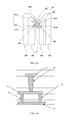
- FIG. 1 is a top schematic diagram of an array substrate according to an embodiment of the present disclosure.
- the array substrate includes a display region 100 and a frame region 200 .
- the frame region 200 includes a drive circuit region 201 and a wire region 202 .
- the wire region 202 there are formed a plurality of first signal wires 1 for connecting driving circuits (not shown in FIG. 1 ) in the drive circuit region 201 with components in the display region 100 .
- FIG. 2 schematically illustrates a cross section of an example of the first signal wire. Referring to FIG.
- the first signal wire 1 may include a stack of a first conductive layer 11 and a second conductive layer 12 , and an insulating layer 13 disposed between the first and the second conductive layers 11 and 12 .
- a first via 14 is formed through the first insulating layer 13 , such that the first and the second conductive layers 11 and 12 can be electrically coupled.
- FIG. 1 there are multiple connecting wires 3 disposed in the wire region 202 .
- the connecting wires 3 are configured to electrically couple a plurality of gate drive units (not shown in FIG. 1 ) in the wire region 202 with the first signal wires 1 , such that drive signals can be transmitted from the first signal wires 1 to the gate drive units through the connecting wires 3 .
- FIG. 3 schematically illustrates an example of a connection mode between the first signal wire and the connecting wire.
- the connecting wire 3 may be electrically connected with the first conductive layer 11 of the first signal 1 through a second via 4 .
- the connecting wire 3 may be connected with the first conductive layer 11 of the first signal wire 1 , so as to establish electrical connection with the first signal wire. It should be noted that the present disclosure is not limited by such configuration. In some embodiments, the electrical connection may be established by connecting the connecting wire 3 with the second conductive layer 12 of the first signal wire 1 .
- the connecting wires 3 may be coupled with other drive units, so that drive signals can be transmitted to these drive units.
- FIG. 4 is a cross sectional view of the display region 100 according to disclosed embodiments.
- the display region 100 includes a gate layer 5 in which gate electrodes are formed, a source/drain layer 6 in which source and drain electrodes are formed, a pixel electrode layer 7 in which pixel electrodes are formed, a common electrode layer 8 in which common electrodes are formed, and a signal transmitting wire layer 9 in which signal transmitting wires are formed.
- the common electrode layer 8 may have a plurality of touch units formed therein.
- the touch units may function as common electrodes in a display period, and also function as touch electrodes in a touch period. Accordingly, the signal transmitting wires in the signal transmitting wire layer 9 are electrically connected with the touch units, so as to transmit common voltage signals to the touch units in the display period, and transmit touch signals to the touch units in the touch period.
- FIG. 5 is a schematic cross-sectional view of the array substrate according to disclosed embodiments.
- the first conductive layer 11 of the first signal wire 1 in the wire region is disposed on the same layer with the gate layer 5 in the display region, and the connecting wire 3 is disposed on the same layer with the source/drain layer 6 .
- layers and/or components being disposed on the same layer refers to that these layers and/or components are disposed at the same or substantially the same height. The height described herein is measured in a direction perpendicular to the array substrate or a display panel including the array substrate. It should be noted that the present disclosure may not be limited by such configuration.
- the first conductive layer 11 may be disposed on the same layer with the source/drain layer 6
- the connecting wire 3 may be disposed on the same layer with the gate layer 5 .
- FIGS. 7 to 9 are schematic cross-sectional view of other examples of the array substrate. Specifically, optional positions of the second conductive layer 12 are illustrated. As shown in FIG. 7 , in some embodiments, the second conductive layer 12 may be disposed on the same layer with the pixel electrode layer 7 . As shown in FIG. 8 , in some embodiments, the second conductive layer 12 may be disposed on the same layer with the common electrode layer 8 . As shown in FIG. 9 , in some embodiments, the second conductive layer 12 may be disposed on the same layer with the signal transmitting wire layer 9 .
- both the first conductive layer 11 and the second conductive layer 12 are disposed on the same layer with two of the layers in the display region.
- the present disclosure is not limited by such configuration.
- only one of the first conductive layer 11 and the second conductive layer 12 is disposed on the same layer with one of the layers in the display region 100 .
- none of the first conductive layer 11 and the second conductive layer 12 is disposed on the same layer with any one layer in the display region 100 .
- the second conductive layer 12 is disposed on the same layer with the pixel electrode layer 7 , and the pixel electrodes in the pixel electrode layer 7 may be transparent electrodes. In such occasion, the second conductive layer also may be formed as a transparent electrode. As such, the second conductive layer 12 and the pixel electrode layer 7 can be formed in the same process, which means that the whole formation process of the array substrate can be simplified. Therefore, production efficiency may be improved, and cost may be reduced.
- the second conductive layer 12 is disposed on the same layer with the signal transmitting wire layer 9 , and the signal transmitting wire layer 9 may be formed as a metal wire layer to reduce the resistance thereof. In such occasion, the second conductive layer also may be formed as a metal conductive layer.
- the second conductive layer 12 and the signal transmitting wire layer 9 can be formed in the same process, which means that the whole formation process of the array substrate can be simplified. Therefore, production efficiency may be improved, and cost may be reduced. Furthermore, using metal material to form the second conductive layer 12 can reduce the resistance thereof, which means that the first signal wire 1 can be formed narrower to obtain the same resistance compared with other material. Accordingly, the frame region of the array substrate can be further reduced. Similarly, in some embodiments, the second conductive layer 12 may be formed on the same layer with the common electrode layer 8 , and formed with a material the same as that of the common electrode layer 8 .
- the wire region 202 further includes a plurality of second signal wires 2 .
- FIG. 10 is a schematic cross-sectional view of an example of the second signal wire according to disclosed embodiments.
- the second signal wire 2 includes a stack of a third conductive layer 21 , a fourth conductive layer 22 and a fifth conductive layer 23 .
- a second insulating layer 24 is disposed between the third conductive layer 21 and the fourth conductive layer 22
- a third insulating layer 25 is disposed between the fourth conductive layer 22 and the fifth conductive layer 23 .
- a third via 26 is formed between the third conductive layer 21 and the fourth conductive layer 22 , so as to electrically connect the third conductive layer 21 and the fourth conductive layer 22 .
- a fourth via 27 is formed between the fourth conductive layer 22 and the fifth conductive layer 23 , so as to electrically connect the fourth conductive layer 22 and the fifth conductive layer 23 .
- any one of the third conductive layer 21 , the fourth conductive layer 22 and the fifth conductive layer 23 may be disposed not on the same layer with any one of the gate layer 5 , the source/drain layer 6 , the pixel electrode layer 7 , the common electrode layer 8 and the signal transmitting wire layer 9 .
- any one of the third conductive layer 21 , the fourth conductive layer 22 and the fifth conductive layer 23 may be disposed on the same layer with any one of the gate layer 5 , the source/drain layer 6 , the pixel electrode layer 7 , the common electrode layer 8 and the signal transmitting wire layer 9 .
- the third conductive layer 21 , the fourth conductive layer 22 and the fifth conductive layer 23 are not all set on the same layer, and they are electrically connected with each other, the width of the wire region can be reduced under the circumstance that the resistance value remains. Therefore, the area of the frame region of the array substrate can be reduced.
- FIGS. 11 to 20 are schematic across-sectional views of array substrates according to disclosed embodiments.
- the third conductive layer 21 is disposed on the same layer with the gate layer 5 ;
- the fourth conductive layer 22 is disposed on the same layer with the source/drain layer 6 ;
- the fifth conductive layer 23 is disposed on the same layer with the pixel electrode layer 7 .
- the third conductive layer 21 is disposed on the same layer with the gate layer 5 ; the fourth conductive layer 22 is disposed on the same layer with the source/drain layer 6 ; and the fifth conductive layer 23 is disposed on the same layer with the common electrode layer 8 .
- the third conductive layer 21 is disposed on the same layer with the gate layer 5 ; the fourth conductive layer 22 is disposed on the same layer with the source/drain layer 6 ; and the fifth conductive layer 23 is disposed on the same layer with the signal transmitting wire layer 9 .
- the third conductive layer 21 is disposed on the same layer with the gate layer 5 ; the fourth conductive layer 22 is disposed on the pixel electrode layer 7 ; and the fifth conductive layer 23 is disposed on the same layer with the common electrode layer 8 .
- the third conductive layer 21 is disposed on the same layer with the gate layer 5 ; the fourth conductive layer 22 is disposed on the pixel electrode layer 7 ; and the fifth conductive layer 23 is disposed on the same layer with the signal transmitting wire layer 9 .
- the third conductive layer 21 is disposed on the same layer with the gate layer 5 ; the fourth conductive layer 22 is disposed on the common electrode layer 8 ; and the fifth conductive layer 23 is disposed on the same layer with the signal transmitting wire layer 9 .
- the third conductive layer 21 is disposed on the source/drain layer 6 ; the fourth conductive layer 22 is disposed on the pixel electrode layer 7 ; and the fifth conductive layer 23 is disposed on the same layer with the common electrode layer 8 .
- the third conductive layer 21 is disposed on the source/drain layer 6 ; the fourth conductive layer 22 is disposed on the pixel electrode layer 7 ; and the fifth conductive layer 23 is disposed on the same layer with the signal transmitting wire layer 9 .
- the third conductive layer 21 is disposed on the source/drain layer 6 ; the fourth conductive layer 22 is disposed on the common electrode layer 8 ; and the fifth conductive layer 23 is disposed on the same layer with the signal transmitting wire layer 9 .
- the third conductive layer 21 is disposed on the pixel electrode layer 7 ; the fourth conductive layer 22 is disposed on the common electrode layer 8 ; and the fifth conductive layer 23 is disposed on the same layer with the signal transmitting wire layer 9 .
- FIG. 21 schematically illustrates a flow chart of the process for forming the array substrate, which includes:
- the method includes: providing the first substrate; forming a conductive layer on the first surface of the first substrate and etching the conductive layer to forming the first conductive layer 11 in the first signal wire region of the wire region disposed on the first surface of the first substrate; forming the first insulating layer 13 on the first conductive layer 11 to completely overlay the first conductive layer 11 ; etching the first insulating layer 13 to form a through via partially exposing the first conductive layer 11 , and forming the first via 14 in the through via, such that the first via 14 is in contact with the first conductive layer 11 ; and forming a conductive layer on the first insulating layer 13 , and etching the conductive layer to form the second conductive layer 12 in the first signal wire region, such that the second conductive layer 12 is electrically connected with the first conductive layer 11 through the first via 14 .
- the method may further include: forming, in the wire region disposed on the first surface of the first substrate, a plurality of gate drive units and a plurality of connecting wires 3 electrically connected with the gate drive units.
- Each of the connecting wires 3 is electrically connected with one of the first signal wires 1 through a second via 4 , such that drive signals can be transmitted from the first signal wires 1 to the gate drive units.
- the connecting wire 3 and the second conductive layer 12 may be formed on opposite sides of the first conductive layer 11 , such that the connecting wire 3 can be electrically connected with the first conductive layer 11 , i.e., electrical connection between the connecting wire 3 and the first signal wire 1 can be established.
- the connecting wire 3 and the first conductive layer 11 may be formed on opposite sides of the second conductive layer 12 , such that the connecting wire 3 can be electrically connected with the second conductive layer 12 , i.e., electrical connection between the connecting wire 3 and the first signal wire 1 can be established.
- the connecting wire 3 may be formed between the first conductive layer 11 and the second conductive layer 12 , such that the connecting wire 3 can be electrically connected with both the first conductive layer 11 and the second conductive layer 12 , i.e., electrical connection between the connecting wire 3 and the first signal wire 1 can be established.
- the connecting wire 3 may be used for providing drive signals to other drive units.
- the method may further include: forming, in the display region disposed on the first surface of the first substrate, a gate layer 5 , a source/drain layer 6 , a pixel electrode layer 7 , a common electrode layer 8 and a signal transmitting wire layer 9 .
- the common electrode layer 8 may have a plurality of touch units formed therein.
- the touch units may function as common electrodes in a display period, and also function as touch electrodes in a touch period. Accordingly, signal transmitting wires formed in the signal transmitting wire layer 9 are electrically connected with the touch units, so as to transmit common voltage signals to the touch units in the display period, and transmit touch signals to the touch units in the touch period.
- the first conductive layer 11 and the gate layer 5 may be formed in the same process, and the connecting wire 3 and the source/drain layer 6 may be formed in the same process, such that the whole formation process of the array substrate can be simplified. Therefore, production efficiency may be improved, and cost may be reduced.
- the first conductive layer 11 and the source/drain layer 6 may be formed in the same process, and the connecting wire 3 and the gate layer 5 may be formed in the same process, such that the whole formation process of the array substrate can be simplified. Therefore, production efficiency may be improved, and cost may be reduced.
- the first conductive layer 11 and the connecting wire 3 may be formed in individual processes without being formed with any other component.
- the second conductive layer 12 it may be formed in an individual process, or in the same process with the pixel electrode layer 7 , the common electrode layer 8 or the signal transmitting wire layer 9 , such that the whole formation process of the array substrate can be simplified. Therefore, production efficiency may be improved, and cost may be reduced.
- the method may further include some steps as illustrated in FIG. 22 , which are described hereinafter.
- the method includes:
- first insulating layer 13 on the first conductive layer 11 to completely overlay the first conductive layer 11 and the third conductive layer 21 ;
- the first conductive layer 11 and the third conductive layer 21 may be formed in the same process.
- the second conductive layer 12 and the fifth conductive layer 23 may be formed in the same process.
- the connecting wires 3 and the fourth conductive layer 22 may be formed in the same process.
- the first conductive layer 11 , the second conductive layer 12 , the third conductive layer 21 , the fourth conductive layer 22 , the fifth conductive layer 23 and the connecting wires 3 are respectively formed in individual processes without being formed with any other component.
- any one of the third conductive layer 21 , the fourth conductive layer 22 and the fifth conductive layer 23 may be in the same process with any one of the gate layer 5 , the source/drain layer 6 , the pixel electrode layer 7 , the common electrode layer 8 and the signal transmitting wire layer 9 .
- the third conductive layer 21 , the fourth conductive layer 22 and the fifth conductive layer 23 are not all set on the same layer, and they are electrically connected with each other, the width of the first signal wire 1 and the second signal 2 can be reduced under the circumstance that the resistance value remains. Therefore, the area of the frame region of the array substrate can be reduced.
- the wire region includes a plurality of first signal wires 1 each of which has two electrically coupled conductive layers 11 and 12 . That means, to obtain the same resistance value as that in prior art, the first signal wires 1 in the present disclosure can be formed with a reduced width. Therefore, if the quantity of the wires remains the same, the area of the wire region 202 in the array substrate may be smaller due to the reduced width, thereby reducing the area of the frame region of a display panel including such an array substrate.
- the array substrate may also include components as illustrated in FIG. 1 , i.e., the array substrate also includes a display region 100 and a frame region 200 .
- the frame region 200 includes a drive circuit region 201 and a wire region 202 .
- the wire region 202 there are formed a plurality of wires for connecting components in the drive circuit region 201 with components in the display region 100 .
- the array substrate further includes some components as illustrated in FIG. 23 .
- In the wire region 202 there are formed a first signal wire layer 10 stacked with a second signal wire layer 20 .
- the first signal wire layer 10 includes a plurality of first signal wires extending along a first direction
- the second signal wire layer 20 includes a plurality of second signal wires extending along the first direction. Furthermore, at least one of the first signals wires and one of the second signal wires are at least partially overlapped in a direction perpendicular to the array substrate. In such configuration, the first and the second signal wires, which are conventionally disposed on the same layer, are disposed in different layers which are stacked with each other. Therefore, to arrange the wires with the same quantity as in the prior art, the wires required to be formed in each of the layers in this embodiment can be reduced.
- the wire region of the array substrate can have a smaller size, and thus the whole frame region of a display panel including such an array substrate can also be smaller.
- the first direction may extend along a length direction of the frame region.
- FIG. 1 there are multiple gate drive units (not shown in FIG. 1 ) and multiple connecting wires 3 disposed in the wire region 202 .
- the connecting wires 3 are configured to provide drive signals 1 to the gate drive units.
- signals transmitted through the first signal wire and the second signal wires may be different. In some embodiments, signals transmitted through the first signal wire and the second signal wires may be the same.
- the connecting wires 3 may be connected with the first signal wires in the first signal wire layer 10 . In some embodiments, the connecting wires 3 may be connected with the second signal wires in the second signal wire layer 20 . In some embodiments, some of the connecting wires 3 may be connected with the first signal wires in the first signal wire layer 10 , some of the connecting wires 3 may be connected with the second signal wires in the second signal wire layer 20 .
- the display region 100 includes a gate layer 5 in which gate electrodes are formed, a source/drain layer 6 in which source and drain electrodes are formed, a pixel electrode layer 7 in which pixel electrodes are formed, a common electrode layer 8 in which common electrodes are formed, and a signal transmitting wire layer 9 in which signal transmitting wires are formed.
- the common electrode layer 8 may have a plurality of touch units formed therein. The touch units may function as common electrodes in a display period, and also function as touch electrodes in a touch period. Accordingly, the signal transmitting wires in the signal transmitting wire layer 9 are electrically connected with the touch units, so as to transmit common voltage signals to the touch units in the display period, and transmit touch signals to the touch units in the touch period.
- any one of the first signal wire layer 10 and the second signal wire layer 20 may be disposed not on the same layer with any one of the gate layer 5 , the source/drain layer 6 , the pixel electrode layer 7 , the common electrode layer 8 and the signal transmitting wire layer 9 . In some embodiments, any one of the first signal wire layer 10 and the second signal wire layer 20 may be disposed on the same layer with any one of the gate layer 5 , the source/drain layer 6 , the pixel electrode layer 7 , the common electrode layer 8 and the signal transmitting wire layer 9 .
- the present disclosure is not limited by specific positions of the above layers, as long as the first signal wire layer 10 and the second signal wire layer 20 are not set on the same layer, and they are electrically insulated with each other.
- the wire region 202 further includes a third signal wire layer 40 which is electrically insulated from both the first signal wire layer 10 and the second signal wire layer 20 .
- the third signal wire layer 40 includes a plurality of third signal wires extending along the first direction.
- the third signal wire layer may also at least partially overlap with any one of the first signal wire layer 10 and the second signal wire layer 20 in the direction perpendicular to the array substrate. Therefore, to arrange the wires with the same quantity as in the prior art, the wires required to be formed in each of the layers in this embodiment can be reduced. As such, the wire region of the array substrate can have a smaller size, and thus the whole frame region of a display panel including such an array substrate can also be smaller.
- signal wires in the first, the second and the third signal wire layers may be the same, or different, or partially the same, which is not limited in the present disclosure.
- FIG. 24 schematically illustrates one embodiment in which the third signal wires partially overlap the first signal wires in the direction perpendicular to the array substrate.
- FIG. 25 schematically illustrates one embodiment in which the third signal wires partially overlap the second signal wires in the direction perpendicular to the array substrate.
- FIG. 26 schematically illustrates one embodiment in which the third signal wires partially overlap both the first signal wires and the second signal wires in the direction perpendicular to the array substrate.
- the third signal wire layer 40 may be disposed not on the same layer with any one of the gate layer 5 , the source/drain layer 6 , the pixel electrode layer 7 , the common electrode layer 8 and the signal transmitting wire layer 9 . In some embodiments, the third signal wire layer 40 may be disposed on the same layer with any one of the gate layer 5 , the source/drain layer 6 , the pixel electrode layer 7 , the common electrode layer 8 and the signal transmitting wire layer 9 . As such, the thickness of the array substrate may be reduced.
- FIGS. 27 to 36 schematically illustrate how to dispose the signal wire layers according to disclosed embodiments.
- the first signal wire layer 10 is disposed on the same layer with the gate layer 5 ;
- the second signal wire layer 20 is disposed on the same layer with the source/drain layer 6 ;
- the third signal wire layer 40 is disposed on the same layer with the pixel electrode layer 7 .
- the first signal wire layer 10 is disposed on the same layer with the gate layer 5 ; the second signal wire layer 20 is disposed on the same layer with the source/drain layer 6 ; and the third signal wire layer 40 is disposed on the same layer with the common electrode layer 8 .
- the first signal wire layer 10 is disposed on the same layer with the gate layer 5 ; the second signal wire layer 20 is disposed on the same layer with the source/drain layer 6 ; and the third signal wire layer 40 is disposed on the same layer with the signal transmitting wire layer 9 .
- the first signal wire layer 10 is disposed on the same layer with the gate layer 5 ; the second signal wire layer 20 is disposed on the pixel electrode layer 7 ; and the third signal wire layer 40 is disposed on the same layer with the common electrode layer 8 .
- the first signal wire layer 10 is disposed on the same layer with the gate layer 5 ; the second signal wire layer 20 is disposed on the pixel electrode layer 7 ; and the third signal wire layer 40 is disposed on the same layer with the signal transmitting wire layer 9 .
- the first signal wire layer 10 is disposed on the same layer with the gate layer 5 ; the second signal wire layer 20 is disposed on the common electrode layer 8 ; and the third signal wire layer 40 is disposed on the same layer with the signal transmitting wire layer 9 .
- the first signal wire layer 10 is disposed on the source/drain layer 6 ; the second signal wire layer 20 is disposed on the pixel electrode layer 7 ; and the third signal wire layer 40 is disposed on the same layer with the common electrode layer 8 .
- the first signal wire layer 10 is disposed on the source/drain layer 6 ; the second signal wire layer 20 is disposed on the pixel electrode layer 7 ; and the third signal wire layer 40 is disposed on the same layer with the signal transmitting wire layer 9 .
- the first signal wire layer 10 is disposed on the source/drain layer 6 ; the second signal wire layer 20 is disposed on the common electrode layer 8 ; and the third signal wire layer 40 is disposed on the same layer with the signal transmitting wire layer 9 .
- the first signal wire layer 10 is disposed on the pixel electrode layer 7 ; the second signal wire layer 20 is disposed on the common electrode layer 8 ; and the third signal wire layer 40 is disposed on the same layer with the signal transmitting wire layer 9 .
- first signal wire layer 10 the second signal wire layer 20 and the third signal wire layer 40 may be interchanged, and positions of the pixel electrode layer 7 , the common electrode 8 and the signal transmitting wire layer 9 also may be interchanged.
- the layers on the same layer may be formed with the same material, such that they can be formed in the same process to reduce the manufacturing processes. Therefore, formation efficiency may be improved and cost may be reduced.
- the wires required to be formed in each of the layers in the present disclosure can be reduced.
- the wire region of the array substrate can have a smaller size, and thus the whole frame region of a display panel including such an array substrate can also be smaller.
- the display panel includes an array substrate 300 and a color film substrate 400 which are face to face with each other.
- a liquid crystal display layer 500 is disposed between the array substrate 300 and the color film substrate 400 .
- the array substrate 300 may be any one of the array substrate described in above embodiments.
- the array substrate provided in embodiments of the present disclosure has a smaller wire region, compared with conventional array substrates and under the circumstance that the wire quantity is the same, it can have a smaller frame region. Therefore, the display panel including such an array substrate may have a smaller frame region.
- FIG. 38 is a schematic diagram of a display panel integrated with a touch control function according to an embodiment of the present disclosure.
- the display panel 3810 includes a substrate 3820 , multiple display pixels PL, multiple data lines DL and multiple touch control signal lines TPL.
- the multiple data lines DL and multiple touch control signal lines TPL are arranged on the substrate 3820 .
- the multiple data lines DL are configured to supply display signals to the display pixels PL.
- the multiple touch control signal lines TPL are configured to transmit control signals for the touch control electrodes TPE.
- lead lines of the multiple data lines DL includes first lead lines C 1
- lead lines of the multiple touch control signal lines TPL includes second lead lines C 2 .
- the data lines DL are connected to an integrated circuit IC through the first lead lines C 1 .
- the integrated circuit IC supplies the display signals to each of the display pixels PL through the data lines DL.
- the touch control signal lines TPL are connected to the integrated circuit IC through the second lead lines C 2 .
- the integrated circuit IC supplies touch control driving signals to each of the touch control electrodes TPE through the touch control signal lines TPL.
- touch control detecting signals generated by the touch control electrodes TPE are inputted into the integrated circuit IC for processing through the touch control signal lines TPL.
- the touch control signal lines TPL act as transmitting the control signals.
- the connection pins for the touch control signals are arranged on one or both ends of the integrated circuit IC. Accordingly, the connection pins for the display signals are arranged on the other end or in the middle of the integrated circuit IC.
- the display panel integrated with a touch control function may be a liquid crystal display panel.
- the display panel integrated with a touch control function 3810 includes multiple display pixels PL.
- Each of the display pixels PL includes a pixel electrode, a common electrode, and a thin film transistor.
- the pixel electrode is electrically connected to the drain of the thin film transistor.
- the source of the thin film transistor is electrically connected to the data line DL.
- the gate of the thin film transistor may be electrically connected to a scanning line SL.
- the scanning line SL controls the thin film transistor to be turned on or off through a signal generated by the gate drive unit 3850 .
- the scanning lines SL control the display signal carried by the data line DL to be inputted into the display pixel.
- the pixel electrode receives the display signal.
- the common electrode receives the common signal.
- the pixel electrode in the display pixel and the common electrode form an electric field to control the rotation of the liquid crystals so as to achieve displaying.
- the common electrode in each display pixel receives a same common signal.
- the display panel integrated with a touch control function according to the embodiment of the present disclosure includes a common electrode layer.
- the common electrode layer includes multiple sub-electrodes insulated from one another. The sub-electrodes are obtained by dividing the common electrode layer. One sub-electrode may be used as a common electrode for multiple display pixels.
- the sub-electrodes may be reused as the touch control electrodes.
- the display panel integrated with a touch control function may operate in a display operating state or a touch control operating state.
- the display operating state and the touch control operating state may be time multiplexed.
- the display operating state is a normal state for the display panel integrated with a touch control function.
- the sub-electrodes are supplied with the common signals or may be connected to ground.
- the touch control operating state displaying is suspended, and the sub-electrodes transmit the touch control signals through the touch control signal lines.
- the sub-electrodes reused as the touch control electrodes may simplify process of manufacturing the display panel integrated with a touch control function, and may save the manufacturing time and manufacturing cost.
- an additional insulating layer is also required to prevent the touch control electrodes from being interfered by other units. Therefore, the sub-electrodes reused as the touch control electrodes may also simplify a layer structure of the display panel integrated with a touch control function, thereby reducing a thickness of the display panel integrated with a touch control function.
- the touch control function of the display panel integrated with a touch control function can be implemented in a mutual capacitance manner or in a self capacitance manner.
- the sub-electrodes may also have multiple configurations accordingly.
- the common electrode layer includes multiple first stripe-shaped sub-electrodes TPE.
- the first stripe-shaped sub-electrodes TPE may be reused as the touch control electrodes TPE.
- the first stripe-shaped sub-electrodes TPE and the touch control electrodes TPE are the same, and an extending direction of the first stripe-shaped sub-electrodes TPE is the same as that of the data lines DL.
- the multiple first stripe-shaped sub-electrodes TPE are sequentially arranged in a direction intersecting the extension direction of the data lines DL. Specifically, the first stripe-shaped sub-electrodes TPE extend in a direction Y. The data lines DL also extend in the direction Y. The multiple the first stripe-shaped sub-electrodes TPE are sequentially arranged in a direction X. The direction X may intersect with the direction Y. As shown in FIG. 38 , one first stripe-shaped sub-electrode TPE corresponds to multiple display pixels PL, and thus one first stripe-shaped sub-electrode TPE is used as a common electrode of the multiple display pixels PL.
- the first stripe-shaped sub-electrodes TPE is used as either the touch control driving electrode or the touch control detecting electrode in the mutual capacitance touch control manner.
- the touch control driving electrodes may be supplied with pulsed touch control driving signals.
- a capacitor is formed between the touch control driving electrode and the touch control detecting electrode.
- the touch control detecting electrodes output the touch control detecting signals.
- the capacitances at the intersections of the touch control driving electrodes and the touch control detecting electrodes are obtained to form two-dimensional capacitance distribution data for the entire display panel integrated with a touch control function.
- coordinates of the touch position may be calculated.
- FIG. 39 is a schematic diagram of a touch control structure in a mutual capacitance manner according to an embodiment of the present disclosure.
- the first stripe-shaped sub-electrodes TPE may be used as the touch control driving electrodes.
- the touch control signal lines supply the touch control driving signals to the first stripe-shaped sub-electrodes TPE.
- the display panel integrated with a touch control function may further include multiple second stripe-shaped sub-electrodes TPE 2 .
- the multiple the second stripe-shaped sub-electrodes TPE 2 are sequentially arranged in parallel.
- the second stripe-shaped sub-electrodes TPE 2 are configured to supply the touch control detecting signals.
- the second stripe-shaped sub-electrodes TPE 2 may be used as the touch control detecting electrodes.
- An extension direction of the second stripe-shaped sub-electrodes TPE 2 intersects with that of the first stripe-shaped sub-electrodes TPE.
- the first stripe-shaped sub-electrodes TPE extend in the direction Y.
- the second stripe-shaped sub-electrodes TPE 2 extend in the direction X.
- the multiple the second stripe-shaped sub-electrodes TPE 2 are sequentially arranged in parallel in the direction Y.
- the direction X intersects with the direction Y.
- FIG. 40 is a cross-sectional view of a touch control structure in a mutual capacitance manner along the CD line as shown in FIG. 39 according to an embodiment of the present disclosure. As shown in FIG.
- the first stripe-shaped sub-electrodes TPE and the second stripe-shaped sub-electrodes TPE 2 may be arranged on the substrate 3820 .
- the first stripe-shaped sub-electrodes TPE may be arranged between the substrate 3820 and the second stripe-shaped sub-electrode TPE 2 .
- An insulating layer may be arranged between the first stripe-shaped sub-electrode TPE and the second stripe-shaped sub-electrode TPE 2 to make the first stripe-shaped sub-electrodes TPE insulated from the second stripe-shaped sub-electrodes TPE 2 .
- FIG. 41 is a cross-sectional view of a touch control structure in a mutual capacitance manner along the CD line as shown in FIG. 39 according to another embodiment of the present disclosure.
- the first stripe-shaped sub-electrodes TPE are arranged on the substrate 3820 .
- the display panel integrated with a touch control function further includes an opposite substrate 3890 arranged opposite to the substrate 3820 .
- the second stripe-shaped sub-electrodes TPE 2 are arranged on the opposite substrate 3890 .
- the second stripe-shaped sub-electrodes TPE 2 are arranged on a side of the opposite substrate 3890 facing the substrate 3820 . Liquid crystal is filled between the substrate 3820 and the opposite substrate 3890 .
- FIG. 42 is a cross-sectional view of a touch control structure in a mutual capacitance manner along the CD line as shown in FIG. 39 according to another embodiment of the present disclosure.
- the first stripe-shaped sub-electrodes TPE are arranged on a substrate 3820 .
- the display panel integrated with a touch control function may also include an opposite substrate 3890 arranged opposite to the substrate 3820 .
- the second stripe-shaped sub-electrodes TPE 2 are arranged on the opposite substrate 3890 . Different from the relative positions as shown in FIG. 41 , the second stripe-shaped sub-electrodes TPE 2 are arranged on a side of the opposite substrate 3890 away from the substrate 3820 .
- the second stripe-shaped sub-electrodes used as the touch control detecting electrodes are arranged on the side of the first stripe-shaped sub-electrodes used as the touch control driving electrodes away from the substrate.
- a touch control operation is implemented on the side of the first stripe-shaped sub-electrodes away from the substrate, on the side of the opposite substrate away from the first substrate in a case that the opposite substrate exists.
- the second stripe-shaped sub-electrodes that is, the touch control detecting electrodes arranged on the side of the first stripe-shaped sub-electrodes away from the first substrate can make the touch control detecting electrodes closer to a touch control operation surface, which makes the touch control operation greatly affect the touch control detecting electrodes.
- the touch control detecting electrodes generate the touch control signals more accurately, thereby making a result of the touch control operation more accurate.
- the second stripe-shaped sub-electrodes that is, the touch control detecting electrodes are arranged on the side of the opposite substrate away from the substrate, which makes the result of the touch control operation more accurate.
- FIG. 43 is a top view of a display panel integrated with a touch control function in a self capacitance manner according to an embodiment of the present disclosure.
- the display panel integrated with a touch control function includes a common electrode layer.
- the common electrode layer includes multiple square-shaped sub-electrodes TPE arranged in an array.
- the square-shaped sub-electrodes TPE are reused as the touch control electrodes in a self capacitance manner.
- the touch control driving signals are inputted into the touch control electrodes, and the touch control electrodes output the touch control detecting signals at the same time.
- a touch control event occurs on the display panel integrated with a touch control function, a capacitance between the touch control electrode near the touch position and the ground may be changed, and the touch control detecting signal outputted by the touch control electrode is changed.
- Each touch control electrode represents one coordinate point.
- the touch control detecting signals from all the touch control electrodes may be processed to determine the touch position. As shown in FIG.
- each touch control electrode TPE are electrically connected to at least one touch control signal line TPL to ensure that each touch control electrode TPE may independently transmit, through the touch control signal line TPL, the touch control signals (including the touch control driving signal and the touch control detecting signal).
- FIG. 44 is a schematic diagram of a display region of a display panel integrated with a touch control function according to an embodiment of the present disclosure.
- a display region of the display panel integrated with a touch control function includes multiple scanning lines SL, data lines DL, display pixels PL, and thin film transistors TFT.
- the source electrode SOURCE of the thin film transistor TFT is electrically connected to the data line DL.
- the drain electrode DRAIN of the thin film transistor TFT is electrically connected to the display pixel PL.
- the gate electrode GATE of the thin film transistor TFT is electrically connected to the scanning line SL.
- the scanning lines SL control the thin film transistors to be turned on or off via scanning signals generated by a scanning driving circuit.
- the scanning lines SL control the display signal carried by the data line DL to be inputted into the display pixel PL.
- the source electrodes SOURCE and the drain electrodes DRAIN of the thin film transistors TFT and the data lines DL may be formed at the same time by etching a source and drain electrode metal layer.
- the gate electrodes GATE of the thin film transistors and the scanning lines may be formed at the same time by etching a gate electrode metal layer. Since the data lines DL and the scanning lines SL intersect with one another on the substrate and are insulated from one another, the source and drain electrode metal layer and the gate electrode metal layer are not in a same metal layer. Specifically, reference is made to FIG.
- the gate electrode GATE is arranged on the substrate 3820 .
- the source electrode SOURCE and the drain electrode DRAIN are arranged on the gate electrode GATE.
- An insulating layer 250 is arranged between the source and drain electrodes SOURCE and DRAIN and the gate electrode GATE.
- FIG. 46 is a cross-sectional view of a display region of an array substrate according to an embodiment of the present disclosure.
- the display region of the array substrate includes an active layer 384 , a gate layer 385 , a source and drain layer 386 , a pixel electrode layer 387 , a common electrode layer 388 and a signal transmission wire layer 389 .
- the common electrode layer 388 includes multiple electrodes as described above. That is, the multiple electrodes are used as common electrodes during a display stage, and are used as touch electrodes during a touch control stage.
- the signal transmission wire layer 389 includes multiple touch control lines electrically connected to the touch control electrodes. The touch control line supplies a common voltage signal to the touch control electrode in the display stage, and supplies a touch control signal to the touch control electrode in the touch control stage.
- the frame region includes a gate drive unit which includes multiple thin film transistors TFT.
- Each TFT includes a source electrode, a drain electrode, and a gate electrode.
- the gate electrode is electrically connected to a signal lead line of the gate drive unit.
- the gate electrode is further electrically connected to a driving circuit IC through the signal lead line B 1 or B 2 (as shown in FIG. 38 ).
- the signal lead line may be the first signal wire of the present application.
- the signal lead line may be arranged on one layer, or on two or more layers.
- the signal lead line may be arranged on a single layer, and the signal lead line is electrically connected to the gate of TFT.
- the gate of TFT is usually formed on a single layer and arranged on the same layer as the gate layer 385 in the display region.
- FIG. 48 which is a cross-sectional view of a gate structure of a TFT in a gate drive unit along the GH line as shown in FIG. 47 according to an embodiment of the present disclosure
- the gate of TFT includes a stack of a first gate conductive layer 38531 and a second gate conductive layer 38532 , and a first gate insulating layer 38533 located between the first gate conductive layer 38531 and the second gate conductive layer 38532 .
- a first gate via 38534 is arranged between the first gate conductive layer 38531 and the second gate conductive layer 38532 .
- the second gate conductive layer 38532 is electrically connected to the first gate conductive layer 38531 through the first gate via 38534 .
- the second gate conductive layer 38532 of the gate 3853 is located on the same layer as the signal transmission wire layer 389 of the display region.
- the material of the second gate conductive layer 38532 may be the same as the material of the signal transmission wire layer 389 of the display region.
- the signal transmission wire layer 389 may be a metal electrode layer
- the second gate conductive layer 38532 may also be a metal electrode layer. In such a way, the second gate conductive layer 38532 and the signal transmission wire layer 389 can be formed at the same time, thereby simplifying the process.
- the first gate conductive layer 38531 may be formed independently, or may be located on the same layer as the gate layer 385 in the display region, or may be located on the same layer as the source and drain layer 386 , or may be located on the same layer as the pixel electrode layer 387 , or may be located on the same layer as the common electrode layer 388 , which is not limited in the present disclosure, as long as it is ensured that the first gate conductive layer 38531 and the second gate conductive layer 38532 are arranged on different layers, and are electrically connected to each other. Therefore, a gate forming area of the gate drive units is decreased, and the area of the frame region of the substrate is decreased.
- the source 3851 of the TFT includes a first source conductive layer located on the same layer as the active layer 384 of the display region and a second source conductive layer located on the same layer as the source and drain layer 386 of the display region.
- the drain 3852 of the TFT includes a first drain conductive layer located on the same layer as the active layer 384 of the display region and a second drain conductive layer located on the same layer as the source and drain layer 386 of the display region.
- the first source conductive layer and the first drain conductive layer are formed as a whole.
- the first source conductive layer is electrically connected to the second source conductive layer through a via
- the first drain conductive layer is electrically connected to the second drain conductive layer through a via.
- the gate 3853 of the TFT is formed, the gate 3853 is electrically connected to the signal lead line B 1 or B 2 of the gate drive unit 3850 .
- the signal lead line B 1 or B 2 may be arranged in a separate layer different from all the layers in the display region, or may be arranged on a same layer as any one layer in the display region.
- the signal lead line B 1 or B 2 may be located on the same layer as the signal transmission wire layer 389 of the display region.
- the signal lead line B 1 or B 2 may be located on the same layer as any one of the gate conductive layers of the gate of TFT of the gate drive unit.
- the signal lead line B 1 or B 2 may be located on the same layer as any one of the gate conductive layers of the gate of TFT of the gate drive unit and the signal transmission wire layer 389 of the display region. As shown in FIG. 50 , the signal lead line B 1 or B 2 is located on the same layer as the second gate conductive layer 38532 of the gate of TFT of the gate drive unit and the signal transmission line layer 389 of the display region. In this case, the signal transmission line layer 389 , the second gate conductive layer 38532 , and the signal lead line B 1 or B 2 may be formed in one process, thereby simplifying the processes.
- the gate conductive layer 38532 can be directly connected to the signal lead line B 1 or B 2 , thereby simplifying the processes.
- the signal lead line B 1 or B 2 may also be electrically connected to the first gate conductive layer 38531 through a via.
- any one of the two layers of the signal lead line may be arranged on a separate layer different from all the layers in the display region, and may also be arranged on a same layer as any one layer in the display region, as long as the two layers of the signal lead line are not located on the same layer.
- Specific method for arranging the signal lead line can refer to the description of the first signal wire in the embodiments of the present application.
- one layer of the signal lead line is located on the same layer as the signal transmission wire layer 389 of the display region.
- one layer of the signal lead line is located on the same layer as any one layer of the gate of TFT of the gate drive unit.
- one layer of the signal lead line is located on the same layer as any one layer of the gate of TFT of the gate drive unit and the signal transmission wire layer 389 of the display region. As shown in FIG. 51 , one layer of the signal lead line is located on the same layer as the second gate conductive layer 38532 of TFT and the signal transmission wire layer 389 of the display region. In this case, the signal transmission wire layer 389 , the second gate conductive layer 38532 , and one layer of the signal lead line may be formed at the same time, thereby simplifying the process. Another layer of the signal lead line may be formed in a separate layer, or may be located on the same layer as any one layer of the display region other than the signal transmission wire layer 389 .
- the layer of the signal lead line can be directly connected to the second gate conductive layer 38532 , thereby simplifying the process.
- the signal lead line may also be electrically connected to the gate of TFT in other ways, as long as any one layer of the signal lead line is electrically connected to any one of the gate conductive layers of the gate.
- the source is electrically connected to the signal lead line.
- the source is further electrically connected to the driving circuit IC through the signal lead line B 1 or B 2 (as shown in FIG. 38 ).
- the signal lead line may be the first signal wire of the present application.
- the signal lead line may be arranged on one layer, or on two or more layers.
- the signal lead line may be arranged on a single layer, and the signal lead line is electrically connected to the source electrode of TFT.
- the source 3851 of the TFT includes a first source conductive layer 38511 , a second source conductive layer 38512 , a third source conductive layer 38513 and a fourth source conductive layer 38514 .
- the first source conductive layer 38511 is electrically connected to the second source conductive layer 38512 through a first source via.
- the second source conductive layer is electrically connected to the fourth source conductive layer through a second source via.
- the third source conductive layer is electrically connected to the fourth source conductive layer through a third source via.
- the drain 3852 includes a first drain conductive layer and a second drain conductive layer, and the first drain conductive layer and the second drain conductive layer are electrically connected through a first drain via.
- the first source conductive layer and the first drain conductive layer are located on a same layer, and are formed as a whole.
- the fourth source conductive layer 38514 is located on the same layer as the signal transmission wire layer 389 of the display region.
- the gate of TFT is a single layer structure, and is located on the same layer as the gate layer 385 of the display region.
- the first source conductive layer and the first drain conductive layer of TFT are located on the same layer as the active layer 384 of the display region.
- the second source conductive layer and the second drain conductive layer of TFT are located on the same layer as the source and drain layer 386 of the display region.
- the third source conductive layer of TFT is located on the same layer as the pixel electrode layer 387 or the common electrode layer 388 of the display region.
- the fourth source conductive layer 38514 is located on the same layer as the signal transmission wire layer 389 of the display region, and the fourth source conductive layer and the signal transmission wire layer is made of ITO. In such a way, the fourth source conductive layer and the signal transmission wire layer 389 may be formed in one process.
- the source 3851 of the TFT is formed, the source 3851 is electrically connected to the signal lead line B 1 or B 2 of the gate drive unit 3850 , and thus the source 3851 is electrically connected to the driving circuit IC through the signal lead line B 1 or B 2 .
- the signal lead line B 1 or B 2 may be the first signal wire of the present application.
- the signal lead line B 1 or B 2 may be arranged on one layer, or on two or more layers.
- the signal lead line B 1 or B 2 may be arranged in a separate layer different from the layers in the display region, or may be arranged in a same layer as any one layer in the display region.
- the signal lead line B 1 or B 2 may be located on the same layer as the signal transmission wire layer 389 of the display region.
- the signal lead line B 1 or B 2 may be located on the same layer as any one of the source conductive layers of the source of TFT of the gate drive unit.
- the signal lead line B 1 or B 2 may be located on the same layer as any one of the source conductive layers of the source of TFT of the gate drive unit and the signal transmission wire layer 389 of the display region. As shown in FIG. 55 , the signal lead line B 1 or B 2 is located on the same layer as the fourth source conductive layer 38514 of the source of TFT of the gate drive unit and the signal transmission line layer 389 of the display region. In this case, the signal transmission line layer 389 , the fourth source conductive layer 38514 , and the signal lead line B 1 or B 2 may be simultaneously formed, thereby simplifying the process.
- the fourth source conductive layer 38514 can be directly connected to the signal lead line B 1 or B 2 , thereby simplifying the process.
- the signal lead line B 1 or B 2 may also be electrically connected to the first source conductive layer, the second source conductive layer, or the third source conductive layer through a via.
- any one of the two layers of the signal lead line may be arranged on a separate layer different from all the layers in the display region, and may also be arranged on a same layer as any one layer in the display region, as long as the two layers of the signal lead line are not located on the same layer.
- Specific method for arranging the signal lead line can refer to the description of the first signal wire in the embodiments of the present application.
- one layer of the signal lead line is located on the same layer as the signal transmission wire layer 389 of the display region.
- one layer of the signal lead line is located on the same layer as any one layer of the source of TFT of the gate drive unit.
- one layer of the signal lead line is located on the same layer as any one layer of the source of TFT of the gate drive unit and the signal transmission wire layer 389 of the display region. As shown in FIG. 56 , one layer of the signal lead line is located on the same layer as the fourth source conductive layer 38514 of TFT and the signal transmission wire layer 389 of the display region. In this case, the signal transmission wire layer 389 , the fourth source conductive layer 38514 , and one layer of the signal lead line may be formed at the same time, thereby simplifying the process. Another layer of the signal lead line may be formed in a separate layer, or may be located on the same layer as any one layer of the display region other than the signal transmission wire layer 389 .
- the layer of the signal lead line can be directly connected to the fourth source conductive layer 38514 , thereby simplifying the process.
- the signal lead line may also be electrically connected to the gate of TFT in other ways, as long as any one layer of the signal lead line is electrically connected to any one of the source conductive layers of the source.
- the signal lead line B 1 or B 2 may be arranged in a single layer, and is electrically connected to the drain of the TFT.
- a structure of the drain of TFT include four layers, and a structure of the source of TFT include two layers, that is, the structures of the source and the drain in the second case are interchanged, and the signal line B 1 or B 2 is electrically connected to the drain. The details can be referred to the second case.
- the gate of TFT includes a first gate conductive layer 38531 and a second gate conductive layer 38532 .
- the first gate conductive layer is electrically connected to the second gate conductive layer through a first gate via.
- the second gate conductive layer is located on the same layer as the signal transmission wire layer 389 of the display region.
- the first gate conductive layer is located on the same layer as the gate layer 385 of the display region.
- the source 3851 and the drain 3852 are located on the same layer as the source and drain layer 386 of the display region.
- the gate 3853 is electrically connected to the signal lead line B 1 or B 2 of the gate drive unit 3850 , and is further electrically connected to the driving circuit IC through the signal lead line B 1 or B 2 .
- the signal lead line B 1 or B 2 may be the first signal wire of the present application.
- the signal lead line B 1 or B 2 may be arranged on one layer, or on two or more layers.
- the signal lead line B 1 or B 2 may be arranged in a separate layer different from the layers in the display region, or may also be arranged in a same layer as any one layer in the display region.
- the signal lead line B 1 or B 2 may be located on the same layer as the signal transmission wire layer 389 of the display region.
- the signal lead line B 1 or B 2 may be located on the same layer as any one of the gate conductive layers of the gate of TFT of the gate drive unit.
- the signal lead line B 1 or B 2 may be located on the same layer as any one of the gate conductive layers of the gate of TFT of the gate drive unit and the signal transmission wire layer 389 of the display region.
- the signal lead line B 1 or B 2 is located on the same layer as the second gate conductive layer 38532 of the gate of TFT of the gate drive unit and the signal transmission line layer 389 of the display region.
- the signal transmission line layer 389 , the second gate conductive layer 38532 , and the signal lead line B 1 or B 2 may be simultaneously formed, thereby simplifying the process.
- the gate conductive layer 38532 can be directly connected to the signal lead line B 1 or B 2 , thereby simplifying the process.
- the signal lead line B 1 or B 2 may also be electrically connected to the first gate conductive layer 38531 through a via.
- any one of the two layers of the signal lead line may be arranged on a separate layer different from all the layers in the display region, and may also be arranged on a same layer as any one layer in the display region, as long as the two layers of the signal lead line are not located on the same layer.
- Specific method for arranging the signal lead line can refer to the description of the first signal wire in the embodiments of the present application.
- one layer of the signal lead line is located on the same layer as the signal transmission wire layer 389 of the display region.
- one layer of the signal lead line is located on the same layer as any one layer of the gate of TFT of the gate drive unit.
- one layer of the signal lead line is located on the same layer as any one layer of the gate of TFT of the gate drive unit and the signal transmission wire layer 389 of the display region.
- one layer of the signal lead line is located on the same layer as the second gate conductive layer 38532 of TFT and the signal transmission wire layer 389 of the display region.
- the signal transmission wire layer 389 , the second gate conductive layer 38532 , and one layer of the signal lead line may be formed at the same time, thereby simplifying the process.
- Another layer of the signal lead line may be formed in a separate layer, or may be located on the same layer as any one layer of the display region other than the signal transmission wire layer 389 .
- the layer of the signal lead line can be directly connected to the second gate conductive layer 38532 , thereby simplifying the process.
- the signal lead line may also be electrically connected to the gate of TFT in other ways, as long as any one layer of the signal lead line is electrically connected to any one of the gate conductive layers of the gate.
- the display panel 3810 further includes a pressure detecting unit 3860 arranged on the array substrate 3820 configured to detect a touch pressure of a user on the panel.
- a pressure detecting unit 3860 arranged on the array substrate 3820 configured to detect a touch pressure of a user on the panel.
- FIG. 59 schematically illustrates one pressure detecting unit. In practice, two or multiple pressure detecting units can be arranged on the panel.
- FIG. 60 is a schematic diagram of connection of a pressure detecting unit according to another embodiment of the present disclosure.
- FIG. 61 is an equivalent circuit diagram of a pressure detecting unit as shown in FIG. 60 . Reference is made to FIG. 59 to FIG. 61 .
- the pressure detecting unit 3860 may include a semiconductor pressure sensor 41 , a bias voltage applying circuit 42 and a voltage detecting circuit 43 .
- the bias voltage applying circuit 42 is electrically connected with a first connecting terminal 4111 and a second connecting terminal 4112 of the semiconductor pressure sensor 41 respectively, and is configured to apply a bias voltage to the semiconductor pressure sensor 41 .
- the voltage detecting circuit 43 is electrically connected with a third connecting terminal 4123 and a fourth connecting terminal 4124 of the semiconductor pressure sensor 41 respectively, and is configured to obtain a force voltage of the semiconductor pressure sensor 41 .
- a first straight line 411 connecting the first connecting terminal 4111 with the second connecting terminal 4112 intersects with a second straight line 412 connecting the third connecting terminal 4123 with the fourth connecting terminal 4124 .
- the semiconductor pressure sensor 41 is a diffused silicon piezo-resistive pressure sensor. Further illustratively, the semiconductor pressure sensor 41 is a four-terminal diffused silicon piezo-resistive pressure sensor which is formed by forming force resistance gauges on a silicon wafer by ion implantation process and then packaging the same. Compared with a conventional pressure sensor, the above semiconductor pressure sensor has advantages, such as a high output, a small size, automatic temperature compensation, and is easier to be integrated on a touch substrate. If the semiconductor pressure sensor is integrated on the substrate, the area of the semiconductor pressure sensor occupying the substrate is small, and a sensitivity of sensing the touch pressure is high.
- the bias voltage applying circuit 42 includes a first electrode 421 and a second electrode 422 .
- the first electrode 421 is electrically connected with the first connecting terminal 4111 .
- the second electrode 422 is electrically connected with the second connecting terminal 4112 .
- the voltage detecting circuit 43 includes a third electrode 431 and a fourth electrode 432 .
- the third electrode 431 is electrically connected with the third connecting terminal 4123
- the fourth electrode 432 is electrically connected with the fourth connecting terminal 4124 .
- the first electrode 421 and the second electrode 422 are configured to apply a bias voltage to the semiconductor pressure sensor 41 .
- the third electrode 431 and the fourth electrode 432 are configured to obtain a force voltage of the semiconductor pressure sensor 41 .
- the semiconductor pressure sensor 41 is a quadrilateral.
- the first electrode 421 and the second electrode 422 in the bias voltage applying circuit 42 are metal electrodes, and are electrically connected with a first connecting terminal 4111 and a second connecting terminal 4112 on two opposite sides of the semiconductor pressure sensor 41 respectively.
- the third electrode 431 and the fourth electrode 432 in the voltage detecting circuit 43 are both metal electrodes, and are electrically connected with the third connecting terminal 4123 and the fourth connecting terminal 4124 on two additional opposite sides of the semiconductor pressure sensor 41 respectively.
- the force voltage of the semiconductor pressure sensor 41 can be obtained by using the voltage detecting circuit 43 , namely, through the third electrode 431 and the fourth electrode 432 , thereby measuring the touch pressure.
- the measuring the touch pressure can be applied in touch operations, such as touching, releasing, or dragging.
- the semiconductor pressure sensor 41 is a quadrilateral pressure sensor.
- the first electrode 421 , the second electrode 422 , the third electrode 431 and the fourth electrode 432 are respectively connected with four sides of the semiconductor pressure sensor 41 .
- FIG. 63 is a schematic diagram of connection of semiconductor pressure detecting units according to an embodiment of the present disclosure.
- the semiconductor pressure sensor 41 is a quadrilateral pressure sensor.
- a first connecting terminal 4111 , a second connecting terminal 4112 , a third connecting terminal 4123 and a fourth connecting terminal 4124 are arranged on one side of the quadrilateral structure respectively.
- the bias voltage applying circuit includes a first electrode 421 and a second electrode 422 which are electrically connected with the first connecting terminal 4111 and the second connecting terminal 4112 respectively on two opposite sides of the semiconductor pressure sensor 41 .
- the voltage detecting circuit 43 includes a third electrode 431 and a fourth electrode 432 which are electrically connected with the third connecting terminal 4123 and the fourth connecting terminal 4124 respectively on the other two opposite sides of the semiconductor pressure sensor 41 .
- the four electrodes and the semiconductor pressure sensor are made of same material. Such an arrangement can effectively eliminate schottky barriers between the first electrode 421 , the second electrode 422 , the third electrode 431 and the fourth electrode 432 and the semiconductor pressure sensor, which can further enhance sensitivity of the semiconductor pressure sensor.
- the four electrodes are externally connected with corresponding metal electrodes respectively.
- a first metal electrode 141 is arranged at the external of the first electrode 421
- a second metal electrode 142 is arranged at the external of the second electrode 422
- a third metal electrode 143 is arranged at the external of the third electrode 431
- a fourth metal electrode 144 is arranged at the external of the fourth electrode 432 ).
- the first metal electrode 141 , the second metal electrode 142 , the third metal electrode 143 and the fourth metal electrode 144 are arranged for the purpose of electrically connecting and transmitting a signal between the semiconductor pressure sensor 41 and other circuits (such as a processor) on the substrate 1 conveniently. It should be noted that these are only two specific examples provided by the embodiments of the present disclosure, rather than limiting the present disclosure.
- the semiconductor pressure sensor 41 may be a polygonal structure including at least four sides, and the first electrode 421 , the second electrode 422 , the third electrode 431 and the fourth electrode 432 are electrically connected with one side of the semiconductor pressure sensor 41 respectively.
- the first straight line 411 connecting the first connecting terminal 4111 with the second connecting terminal 4112 are orthogonal with the second straight line 412 connecting the third connecting terminal 4123 with the fourth connecting terminal 4124 .
- FIG. 64 is a cross-sectional view of a pressure detecting unit according to an embodiment of the present disclosure.
- the pressure detecting unit has three layers.
- a first layer 51 is electrically connected to a second layer 52 through a via 55
- the second layer 52 is electrically connected to a third layer 53 through a via 54 .
- the first layer 51 may be a low-temperature poly-silicon layer
- the second layer 52 may be a source and drain layer
- the third layer 53 may be a metal electrode layer for forming four electrodes of the semiconductor pressure sensor 41 .
- FIG. 46 is cross-sectional view of a display region of an array substrate according to an embodiment of the present disclosure.
- the display region of the array substrate includes an active layer 384 , a gate layer 385 , a source and drain layer 386 , a pixel electrode layer 387 , a common electrode layer 388 and a signal transmission wire layer 389 .
- Any one of the three layers 51 , 52 , and 53 of the pressure detecting unit according to the embodiment of the present disclosure may be arranged in a separate layer different from all the layers in the display region, or may also be arranged on a same layer as any one layer in the display region, as long as the three layers 51 , 52 , and 53 of the pressure detecting unit are arranged on different layers.
- the third layer 53 of the pressure detecting unit according to the embodiment of the present disclosure may be arranged on a same layer as the signal transmission wire layer 389 of the display region.
- the third layer 53 of the pressure detecting unit is a metal electrode layer configured to form the pressure detecting unit, and the material of the signal transmission wire layer may be selected as the metal electrode layer. Therefore, the metal electrode layer and the signal transmission wire layer may be formed at the same time, thereby simplifying the process.
- the second layer 52 of the pressure detecting unit according to the embodiment of the present disclosure may be arranged on a same layer as the source and drain layer 386 of the display region.
- the first layer 51 of the pressure detecting unit may be arranged on a same layer as the active layer 384 of the display region.
- the material of the active layer 384 is selected as low-temperature poly-silicon such that the first layer 51 of the pressure detecting unit and the active layer 384 of the display region can be formed at the same time.
- the metal electrode of the pressure detecting unit can be made to be electrically connected to the signal lead line B 1 or B 2 of the gate drive unit, and the metal electrode is further electrically connected to the driving circuit IC through the signal lead line B 1 or B 2 , as shown in FIG. 66 .
- the signal lead line B 1 or B 2 may be the first signal wire of the present application.
- the signal lead line B 1 or B 2 may be arranged on one layer, or on two or more layers.
- the signal lead line B 1 or B 2 may be arranged in a separate layer different from all the layers in the display region, or may also be arranged on a same layer as any one layer in the display region.
- the signal lead line B 1 or B 2 may be located on the same layer as the signal transmission wire layer 389 of the display region.
- the signal lead line B 1 or B 2 may be located on the same layer as the third layer (the metal electrode layer) of the pressure detecting unit.
- the signal lead line B 1 or B 2 may be located on the same layer as the third layer of the pressure detecting unit and the signal transmission wire layer 389 of the display region, as shown in FIG.
- the signal transmission line layer 389 , the third layer of the pressure detecting unit, and the signal lead line B 1 or B 2 may be simultaneously formed, thereby simplifying the process.
- the third layer may be directly connected to the signal lead line B 1 or B 2 , thereby simplifying the process.
- the signal lead line B 1 or B 2 may also be electrically connected to the first layer or the second layer of the pressure detecting unit through a via.
- any one of the two layers of the signal lead line may be arranged on a separate layer different from all the layers in the display region, and may also be arranged on a same layer as any one layer in the display region, as long as the two layers of the signal lead line are not located on the same layer.
- Specific method for arranging the signal lead line can refer to the description of the first signal wire in the embodiments of the present application.
- one layer of the signal lead line is located on the same layer as the signal transmission wire layer 389 of the display region.
- one layer of the signal lead line is located on the same layer as the third layer (the metal electrode layer) of the pressure detecting unit.
- one layer of the signal lead line is located on the same layer as the third layer of the pressure detecting unit and the signal transmission wire layer 389 of the display region, as shown in FIG. 68 .
- the signal transmission wire layer 389 , the third layer of the pressure detecting unit, and one layer of the signal lead line may be formed at the same time, thereby simplifying the process.
- Another layer of the signal lead line may be formed in a separate layer, or may be located on the same layer as any one layer of the display region other than the signal transmission wire layer 389 .
- the layer of the signal lead line can be directly connected to the third layer of the pressure detecting unit, thereby simplifying the process.
- the signal lead line may also be electrically connected to the pressure detecting unit in other ways, as long as any one layer of the signal lead line is electrically connected to any one layer of the pressure detecting unit.
Landscapes
- Engineering & Computer Science (AREA)
- Physics & Mathematics (AREA)
- Theoretical Computer Science (AREA)
- General Engineering & Computer Science (AREA)
- General Physics & Mathematics (AREA)
- Power Engineering (AREA)
- Human Computer Interaction (AREA)
- Computer Hardware Design (AREA)
- Microelectronics & Electronic Packaging (AREA)
- Condensed Matter Physics & Semiconductors (AREA)
- Crystallography & Structural Chemistry (AREA)
- Nonlinear Science (AREA)
- Chemical & Material Sciences (AREA)
- Manufacturing & Machinery (AREA)
- Optics & Photonics (AREA)
- Mathematical Physics (AREA)
- Devices For Indicating Variable Information By Combining Individual Elements (AREA)
Abstract
Description
Claims (20)
Priority Applications (1)
| Application Number | Priority Date | Filing Date | Title |
|---|---|---|---|
| US15/620,680 US10152159B2 (en) | 2015-04-01 | 2017-06-12 | Display panel and method for forming an array substrate of a display panel |
Applications Claiming Priority (5)
| Application Number | Priority Date | Filing Date | Title |
|---|---|---|---|
| CN201510152796.7A CN104699349B (en) | 2015-04-01 | 2015-04-01 | A kind of array base palte and preparation method thereof, display panel |
| CN201510152796 | 2015-04-01 | ||
| CN201510152796.7 | 2015-04-01 | ||
| US14/857,632 US9711541B2 (en) | 2015-04-01 | 2015-09-17 | Display panel and method for forming an array substrate of a display panel |
| US15/620,680 US10152159B2 (en) | 2015-04-01 | 2017-06-12 | Display panel and method for forming an array substrate of a display panel |
Related Parent Applications (1)
| Application Number | Title | Priority Date | Filing Date |
|---|---|---|---|
| US14/857,632 Continuation-In-Part US9711541B2 (en) | 2015-04-01 | 2015-09-17 | Display panel and method for forming an array substrate of a display panel |
Publications (2)
| Publication Number | Publication Date |
|---|---|
| US20170277326A1 US20170277326A1 (en) | 2017-09-28 |
| US10152159B2 true US10152159B2 (en) | 2018-12-11 |
Family
ID=59898476
Family Applications (1)
| Application Number | Title | Priority Date | Filing Date |
|---|---|---|---|
| US15/620,680 Active 2035-10-19 US10152159B2 (en) | 2015-04-01 | 2017-06-12 | Display panel and method for forming an array substrate of a display panel |
Country Status (1)
| Country | Link |
|---|---|
| US (1) | US10152159B2 (en) |
Cited By (1)
| Publication number | Priority date | Publication date | Assignee | Title |
|---|---|---|---|---|
| US10838277B2 (en) * | 2018-09-12 | 2020-11-17 | Sharp Kabushiki Kaisha | Image display device with frame region transistor control line including stacked line layers |
Families Citing this family (8)
| Publication number | Priority date | Publication date | Assignee | Title |
|---|---|---|---|---|
| CN104698711B (en) * | 2015-04-01 | 2018-06-01 | 上海天马微电子有限公司 | A kind of array substrate, display panel and electronic equipment |
| CN105487273A (en) * | 2016-01-15 | 2016-04-13 | 京东方科技集团股份有限公司 | Display panel, drive method and manufacturing method thereof and display device |
| JP2018018006A (en) * | 2016-07-29 | 2018-02-01 | 株式会社ジャパンディスプレイ | Display device |
| KR102600592B1 (en) * | 2016-08-29 | 2023-11-10 | 삼성디스플레이 주식회사 | Touch sensor and display device including the same |
| US11144170B2 (en) | 2018-12-17 | 2021-10-12 | Wuhan China Star Optoelectronics Semiconductor Display Technology Co., Ltd. | Display panel and display module |
| US11195900B2 (en) | 2019-09-02 | 2021-12-07 | Wuhan China Star Optoelectronics Semiconductor Display Technology Co., Ltd. | Array substrate with protrusion patterns and method of fabricating same |
| TW202143013A (en) * | 2019-12-30 | 2021-11-16 | 矽創電子股份有限公司 | Touch detecting circuit |
| CN112269490B (en) * | 2020-10-22 | 2024-03-15 | 京东方科技集团股份有限公司 | Display substrate, manufacturing method thereof and display device |
Citations (14)
| Publication number | Priority date | Publication date | Assignee | Title |
|---|---|---|---|---|
| US6850307B2 (en) | 2000-02-18 | 2005-02-01 | Seiko Epson Corporation | Display device substrate, method for manufacturing the display device substrate, liquid-crystal display device, and electronic equipment |
| US20070290967A1 (en) | 2006-06-16 | 2007-12-20 | Lg.Philips Lcd Co., Ltd. | Display device and method of fabricating the same |
| CN201465087U (en) | 2009-05-22 | 2010-05-12 | 比亚迪股份有限公司 | Resistance-type multi touch screen |
| US20100156851A1 (en) | 2008-12-24 | 2010-06-24 | Semiconductor Energy Laboratory Co., Ltd. | Touch Panel and Driving Method Thereof |
| US20120105392A1 (en) | 2010-11-01 | 2012-05-03 | Takahiro Nagami | Liquid Crystal Display Device |
| CN103262012A (en) | 2010-12-09 | 2013-08-21 | 夏普株式会社 | Touch panel, display device provided with same, and method for producing touch panel |
| CN103489879A (en) | 2013-10-11 | 2014-01-01 | 京东方科技集团股份有限公司 | Array substrate, manufacturing method thereof and display device |
| US9035310B2 (en) | 2011-10-05 | 2015-05-19 | Japan Display Inc. | Display device |
| US20150378223A1 (en) | 2014-06-30 | 2015-12-31 | Xiamen Tianma Micro-Electronics Co., Ltd. | Array substrate, method of fabricating the same and liquid crystal display panel |
| US20160291722A1 (en) | 2015-04-01 | 2016-10-06 | Shanghai Tianma Micro-electronics Co., Ltd. | Array Substrate, Display Panel and Display Device |
| US20160291424A1 (en) | 2015-04-01 | 2016-10-06 | Shanghai Tianma Micro-electronics Co., Ltd. | Touch display panel and display apparatus |
| US20160293642A1 (en) | 2015-04-01 | 2016-10-06 | Boe Technology Group Co., Ltd. | Tft array substrate, method of manufacturing the same and display device |
| US20160300863A1 (en) | 2015-04-08 | 2016-10-13 | Japan Display Inc. | Transistor substrate and display device |
| US20170222059A1 (en) * | 2016-01-29 | 2017-08-03 | Wuhan China Star Optoelectronics Technology Co., Ltd. | Array substrate and the manufacturing methods thereof |
-
2017
- 2017-06-12 US US15/620,680 patent/US10152159B2/en active Active
Patent Citations (15)
| Publication number | Priority date | Publication date | Assignee | Title |
|---|---|---|---|---|
| US6850307B2 (en) | 2000-02-18 | 2005-02-01 | Seiko Epson Corporation | Display device substrate, method for manufacturing the display device substrate, liquid-crystal display device, and electronic equipment |
| US20070290967A1 (en) | 2006-06-16 | 2007-12-20 | Lg.Philips Lcd Co., Ltd. | Display device and method of fabricating the same |
| US20100156851A1 (en) | 2008-12-24 | 2010-06-24 | Semiconductor Energy Laboratory Co., Ltd. | Touch Panel and Driving Method Thereof |
| CN201465087U (en) | 2009-05-22 | 2010-05-12 | 比亚迪股份有限公司 | Resistance-type multi touch screen |
| US20120105392A1 (en) | 2010-11-01 | 2012-05-03 | Takahiro Nagami | Liquid Crystal Display Device |
| US20130258614A1 (en) | 2010-12-09 | 2013-10-03 | Sharp Kabushiki Kaisha | Touch panel, display device including the touch panel, and method of manufacturing the touch panel |
| CN103262012A (en) | 2010-12-09 | 2013-08-21 | 夏普株式会社 | Touch panel, display device provided with same, and method for producing touch panel |
| US9035310B2 (en) | 2011-10-05 | 2015-05-19 | Japan Display Inc. | Display device |
| CN103489879A (en) | 2013-10-11 | 2014-01-01 | 京东方科技集团股份有限公司 | Array substrate, manufacturing method thereof and display device |
| US20150378223A1 (en) | 2014-06-30 | 2015-12-31 | Xiamen Tianma Micro-Electronics Co., Ltd. | Array substrate, method of fabricating the same and liquid crystal display panel |
| US20160291722A1 (en) | 2015-04-01 | 2016-10-06 | Shanghai Tianma Micro-electronics Co., Ltd. | Array Substrate, Display Panel and Display Device |
| US20160291424A1 (en) | 2015-04-01 | 2016-10-06 | Shanghai Tianma Micro-electronics Co., Ltd. | Touch display panel and display apparatus |
| US20160293642A1 (en) | 2015-04-01 | 2016-10-06 | Boe Technology Group Co., Ltd. | Tft array substrate, method of manufacturing the same and display device |
| US20160300863A1 (en) | 2015-04-08 | 2016-10-13 | Japan Display Inc. | Transistor substrate and display device |
| US20170222059A1 (en) * | 2016-01-29 | 2017-08-03 | Wuhan China Star Optoelectronics Technology Co., Ltd. | Array substrate and the manufacturing methods thereof |
Non-Patent Citations (1)
| Title |
|---|
| Chinese Application No. 201510152796.7, First Office Action dated Apr. 21, 2017. |
Cited By (1)
| Publication number | Priority date | Publication date | Assignee | Title |
|---|---|---|---|---|
| US10838277B2 (en) * | 2018-09-12 | 2020-11-17 | Sharp Kabushiki Kaisha | Image display device with frame region transistor control line including stacked line layers |
Also Published As
| Publication number | Publication date |
|---|---|
| US20170277326A1 (en) | 2017-09-28 |
Similar Documents
| Publication | Publication Date | Title |
|---|---|---|
| US10152159B2 (en) | Display panel and method for forming an array substrate of a display panel | |
| KR102579368B1 (en) | Display panel with external signal lines under gate drive circuit | |
| US10031615B2 (en) | Touch substrate, touch display panel and method for calculating touch pressure | |
| US10289243B2 (en) | Touch control display device and manufacturing method thereof | |
| US10627941B2 (en) | Integrated touch control display panel and touch display device comprising conductive layer in non-display region | |
| KR102650323B1 (en) | Touch sensor integrated display device with multiple planarization layers | |
| WO2017197934A1 (en) | Array substrate and manufacturing method thereof, and touch display apparatus | |
| US9372360B2 (en) | Touch liquid crystal display device | |
| KR102579383B1 (en) | Touch recognition enabled display panel with asymmetric black matrix pattern | |
| US10338724B2 (en) | Array substrate and method for fabricating the same, and display device and method for driving the same | |
| CN106354347A (en) | Embedded type touch display panel and manufacturing method thereof | |
| WO2017024716A1 (en) | Touch control display panel and drive method therefor, and display device | |
| CN104731412A (en) | Array substrate, display panel and display device | |
| US10739925B2 (en) | Touch screen panel-integrated display device and method for fabricating the same | |
| US10248255B2 (en) | Array substrate, touch display panel and method for calculating touch pressure | |
| CN107315506B (en) | Display substrate, display panel and display device | |
| JP2014149429A (en) | Liquid crystal display device and method for manufacturing liquid crystal display device | |
| WO2017045222A1 (en) | Touch panel, array substrate and manufacturing method therefor | |
| WO2019105102A1 (en) | Touch panel, touch device, and method for manufacturing touch panel | |
| US11226694B2 (en) | Touch display substrate, touch display method and touch display device | |
| WO2015176437A1 (en) | Array substrate and manufacturing method thereof, and touch control display apparatus | |
| US20150338976A1 (en) | Touch display device | |
| US10775659B2 (en) | Array substrate, display device and driving method thereof | |
| JP2019086575A (en) | Display device | |
| WO2017012166A1 (en) | Panel and panel preparation method |
Legal Events
| Date | Code | Title | Description |
|---|---|---|---|
| AS | Assignment |
Owner name: TIANMA MICRO-ELECTRONICS CO/. LTD., CHINA Free format text: ASSIGNMENT OF ASSIGNORS INTEREST;ASSIGNORS:CAO, ZHAOKENG;JIN, HUIJUN;LI, XIAOYE;AND OTHERS;REEL/FRAME:042680/0631 Effective date: 20170612 Owner name: SHANGHAI TIANMA MICRO-ELECTRONICS, CHINA Free format text: ASSIGNMENT OF ASSIGNORS INTEREST;ASSIGNORS:CAO, ZHAOKENG;JIN, HUIJUN;LI, XIAOYE;AND OTHERS;REEL/FRAME:042680/0631 Effective date: 20170612 |
|
| AS | Assignment |
Owner name: SHANGHAI TIANMA MICRO-ELECTRONICS CO., LTD., CHINA Free format text: ASSIGNMENT OF ASSIGNORS INTEREST;ASSIGNORS:CAO, ZHAOKENG;JIN, HUIJUN;LI, XIAOYE;AND OTHERS;REEL/FRAME:042994/0807 Effective date: 20170612 Owner name: TIANMA MICRO-ELECTRONICS CO., LTD., CHINA Free format text: ASSIGNMENT OF ASSIGNORS INTEREST;ASSIGNORS:CAO, ZHAOKENG;JIN, HUIJUN;LI, XIAOYE;AND OTHERS;REEL/FRAME:042994/0807 Effective date: 20170612 |
|
| STCF | Information on status: patent grant |
Free format text: PATENTED CASE |
|
| MAFP | Maintenance fee payment |
Free format text: PAYMENT OF MAINTENANCE FEE, 4TH YEAR, LARGE ENTITY (ORIGINAL EVENT CODE: M1551); ENTITY STATUS OF PATENT OWNER: LARGE ENTITY Year of fee payment: 4 |