US10108898B1 - Package tracking label having activation and deactivation tabs - Google Patents
Package tracking label having activation and deactivation tabs Download PDFInfo
- Publication number
- US10108898B1 US10108898B1 US15/839,847 US201715839847A US10108898B1 US 10108898 B1 US10108898 B1 US 10108898B1 US 201715839847 A US201715839847 A US 201715839847A US 10108898 B1 US10108898 B1 US 10108898B1
- Authority
- US
- United States
- Prior art keywords
- package
- tab
- microprocessor
- activation
- deactivation
- Prior art date
- Legal status (The legal status is an assumption and is not a legal conclusion. Google has not performed a legal analysis and makes no representation as to the accuracy of the status listed.)
- Active
Links
Images


Classifications
-
- G—PHYSICS
- G06—COMPUTING; CALCULATING OR COUNTING
- G06K—GRAPHICAL DATA READING; PRESENTATION OF DATA; RECORD CARRIERS; HANDLING RECORD CARRIERS
- G06K19/00—Record carriers for use with machines and with at least a part designed to carry digital markings
- G06K19/06—Record carriers for use with machines and with at least a part designed to carry digital markings characterised by the kind of the digital marking, e.g. shape, nature, code
- G06K19/067—Record carriers with conductive marks, printed circuits or semiconductor circuit elements, e.g. credit or identity cards also with resonating or responding marks without active components
- G06K19/07—Record carriers with conductive marks, printed circuits or semiconductor circuit elements, e.g. credit or identity cards also with resonating or responding marks without active components with integrated circuit chips
- G06K19/077—Constructional details, e.g. mounting of circuits in the carrier
- G06K19/0772—Physical layout of the record carrier
- G06K19/07722—Physical layout of the record carrier the record carrier being multilayered, e.g. laminated sheets
-
- G—PHYSICS
- G06—COMPUTING; CALCULATING OR COUNTING
- G06K—GRAPHICAL DATA READING; PRESENTATION OF DATA; RECORD CARRIERS; HANDLING RECORD CARRIERS
- G06K19/00—Record carriers for use with machines and with at least a part designed to carry digital markings
- G06K19/06—Record carriers for use with machines and with at least a part designed to carry digital markings characterised by the kind of the digital marking, e.g. shape, nature, code
- G06K19/067—Record carriers with conductive marks, printed circuits or semiconductor circuit elements, e.g. credit or identity cards also with resonating or responding marks without active components
- G06K19/07—Record carriers with conductive marks, printed circuits or semiconductor circuit elements, e.g. credit or identity cards also with resonating or responding marks without active components with integrated circuit chips
- G06K19/0723—Record carriers with conductive marks, printed circuits or semiconductor circuit elements, e.g. credit or identity cards also with resonating or responding marks without active components with integrated circuit chips the record carrier comprising an arrangement for non-contact communication, e.g. wireless communication circuits on transponder cards, non-contact smart cards or RFIDs
-
- G—PHYSICS
- G06—COMPUTING; CALCULATING OR COUNTING
- G06K—GRAPHICAL DATA READING; PRESENTATION OF DATA; RECORD CARRIERS; HANDLING RECORD CARRIERS
- G06K19/00—Record carriers for use with machines and with at least a part designed to carry digital markings
- G06K19/06—Record carriers for use with machines and with at least a part designed to carry digital markings characterised by the kind of the digital marking, e.g. shape, nature, code
- G06K19/067—Record carriers with conductive marks, printed circuits or semiconductor circuit elements, e.g. credit or identity cards also with resonating or responding marks without active components
- G06K19/07—Record carriers with conductive marks, printed circuits or semiconductor circuit elements, e.g. credit or identity cards also with resonating or responding marks without active components with integrated circuit chips
- G06K19/073—Special arrangements for circuits, e.g. for protecting identification code in memory
- G06K19/07309—Means for preventing undesired reading or writing from or onto record carriers
- G06K19/07345—Means for preventing undesired reading or writing from or onto record carriers by activating or deactivating at least a part of the circuit on the record carrier, e.g. ON/OFF switches
-
- G—PHYSICS
- G06—COMPUTING; CALCULATING OR COUNTING
- G06K—GRAPHICAL DATA READING; PRESENTATION OF DATA; RECORD CARRIERS; HANDLING RECORD CARRIERS
- G06K19/00—Record carriers for use with machines and with at least a part designed to carry digital markings
- G06K19/06—Record carriers for use with machines and with at least a part designed to carry digital markings characterised by the kind of the digital marking, e.g. shape, nature, code
- G06K19/067—Record carriers with conductive marks, printed circuits or semiconductor circuit elements, e.g. credit or identity cards also with resonating or responding marks without active components
- G06K19/07—Record carriers with conductive marks, printed circuits or semiconductor circuit elements, e.g. credit or identity cards also with resonating or responding marks without active components with integrated circuit chips
- G06K19/077—Constructional details, e.g. mounting of circuits in the carrier
- G06K19/07749—Constructional details, e.g. mounting of circuits in the carrier the record carrier being capable of non-contact communication, e.g. constructional details of the antenna of a non-contact smart card
- G06K19/07758—Constructional details, e.g. mounting of circuits in the carrier the record carrier being capable of non-contact communication, e.g. constructional details of the antenna of a non-contact smart card arrangements for adhering the record carrier to further objects or living beings, functioning as an identification tag
- G06K19/0776—Constructional details, e.g. mounting of circuits in the carrier the record carrier being capable of non-contact communication, e.g. constructional details of the antenna of a non-contact smart card arrangements for adhering the record carrier to further objects or living beings, functioning as an identification tag the adhering arrangement being a layer of adhesive, so that the record carrier can function as a sticker
-
- G—PHYSICS
- G06—COMPUTING; CALCULATING OR COUNTING
- G06K—GRAPHICAL DATA READING; PRESENTATION OF DATA; RECORD CARRIERS; HANDLING RECORD CARRIERS
- G06K19/00—Record carriers for use with machines and with at least a part designed to carry digital markings
- G06K19/06—Record carriers for use with machines and with at least a part designed to carry digital markings characterised by the kind of the digital marking, e.g. shape, nature, code
- G06K19/067—Record carriers with conductive marks, printed circuits or semiconductor circuit elements, e.g. credit or identity cards also with resonating or responding marks without active components
- G06K19/07—Record carriers with conductive marks, printed circuits or semiconductor circuit elements, e.g. credit or identity cards also with resonating or responding marks without active components with integrated circuit chips
- G06K19/077—Constructional details, e.g. mounting of circuits in the carrier
- G06K19/07749—Constructional details, e.g. mounting of circuits in the carrier the record carrier being capable of non-contact communication, e.g. constructional details of the antenna of a non-contact smart card
- G06K19/07773—Antenna details
-
- G—PHYSICS
- G06—COMPUTING; CALCULATING OR COUNTING
- G06K—GRAPHICAL DATA READING; PRESENTATION OF DATA; RECORD CARRIERS; HANDLING RECORD CARRIERS
- G06K19/00—Record carriers for use with machines and with at least a part designed to carry digital markings
- G06K19/06—Record carriers for use with machines and with at least a part designed to carry digital markings characterised by the kind of the digital marking, e.g. shape, nature, code
- G06K19/067—Record carriers with conductive marks, printed circuits or semiconductor circuit elements, e.g. credit or identity cards also with resonating or responding marks without active components
- G06K19/07—Record carriers with conductive marks, printed circuits or semiconductor circuit elements, e.g. credit or identity cards also with resonating or responding marks without active components with integrated circuit chips
- G06K19/077—Constructional details, e.g. mounting of circuits in the carrier
- G06K19/07749—Constructional details, e.g. mounting of circuits in the carrier the record carrier being capable of non-contact communication, e.g. constructional details of the antenna of a non-contact smart card
- G06K19/07798—Constructional details, e.g. mounting of circuits in the carrier the record carrier being capable of non-contact communication, e.g. constructional details of the antenna of a non-contact smart card part of the antenna or the integrated circuit being adapted for rupturing or breaking, e.g. record carriers functioning as sealing devices for detecting not-authenticated opening of containers
-
- G—PHYSICS
- G06—COMPUTING; CALCULATING OR COUNTING
- G06Q—INFORMATION AND COMMUNICATION TECHNOLOGY [ICT] SPECIALLY ADAPTED FOR ADMINISTRATIVE, COMMERCIAL, FINANCIAL, MANAGERIAL OR SUPERVISORY PURPOSES; SYSTEMS OR METHODS SPECIALLY ADAPTED FOR ADMINISTRATIVE, COMMERCIAL, FINANCIAL, MANAGERIAL OR SUPERVISORY PURPOSES, NOT OTHERWISE PROVIDED FOR
- G06Q10/00—Administration; Management
- G06Q10/08—Logistics, e.g. warehousing, loading or distribution; Inventory or stock management
- G06Q10/083—Shipping
- G06Q10/0833—Tracking
-
- G—PHYSICS
- G08—SIGNALLING
- G08B—SIGNALLING OR CALLING SYSTEMS; ORDER TELEGRAPHS; ALARM SYSTEMS
- G08B13/00—Burglar, theft or intruder alarms
- G08B13/22—Electrical actuation
- G08B13/24—Electrical actuation by interference with electromagnetic field distribution
- G08B13/2402—Electronic Article Surveillance [EAS], i.e. systems using tags for detecting removal of a tagged item from a secure area, e.g. tags for detecting shoplifting
- G08B13/2405—Electronic Article Surveillance [EAS], i.e. systems using tags for detecting removal of a tagged item from a secure area, e.g. tags for detecting shoplifting characterised by the tag technology used
- G08B13/2414—Electronic Article Surveillance [EAS], i.e. systems using tags for detecting removal of a tagged item from a secure area, e.g. tags for detecting shoplifting characterised by the tag technology used using inductive tags
- G08B13/242—Tag deactivation
Abstract
A method of tracking a package. The method includes applying a package label to a package in which the package label comprises an antenna circuit, an activation tab configured to activate the antenna circuit, and a deactivation tab configured to deactivate the antenna circuit. The method also includes activating the antenna circuit by removing the activation tab and periodically transmitting a signal by the antenna circuit upon activation. The signal comprises information that identifies the package. The method also includes receiving the signal and using the information in the signal to track a location of the package.
Description
The present Application for Patent claims the benefit of U.S. Provisional Application No. 62/558,843, entitled “PACKAGE TRACKING LABEL”, filed Sep. 14, 2017, assigned to the assignee hereof, and expressly incorporated herein by reference in its entirety.
This disclosure relates generally to package tracking, and more specifically, but not exclusively, to package tracking using a single use label.
Package delivery has always been an important part of commerce, and the ability to identify a package and its location may be considered core to companies that ship packages from one location to another. For example, tracking packages is important to organizations of all kinds, whether it be a company keeping track of inventory to be sold in its stores, or a package delivery provider keeping track of packages being transported through its delivery network. To provide quality service, an organization typically creates and maintains a highly organized network for tracking its items—packages, people, objects, etc.
Conventionally, this tracking function may be provided by a variety of known mechanisms and systems. Machine-readable barcodes are one way organizations keep track of items. A retailer, for example, may use bar codes on items in its inventory. For example, items to be sold in a retailer's store may each be labeled with a different machine-readable bar code. In order to keep track of inventory, the retailer typically scans or otherwise captures an image of the bar code on each item so that a back-end part of the retailer's operation can keep track of what is coming in and leaving their possession from suppliers. In addition, when an item is sold to a consumer, the bar code for that item is scanned or captured to track sales and inventory levels.
Similarly, a package delivery provider may utilize machine-readable bar codes by associating a bar code with packages to be delivered to a recipient. For example, a package may have a bar code corresponding to a tracking number for that package. Each time the package goes through a transit checkpoint (e.g., the courier taking initial control of the package, the package being temporarily placed in a storage facility while being moved from a pickup point to a delivery location, and the package being delivered to the recipient, etc.), the package's bar code may be scanned. Bar codes, however, have the disadvantage that personnel must manually scan each bar code on each item in order to effectively track the items.
Thus, there remains a need for an improved system that may provide more robust identification and tracking of packages and do so in a cost effective manner. Accordingly, there is a need for systems, apparatus, and methods that overcome the deficiencies of conventional approaches including the methods, system and apparatus provided hereby.
The following presents a simplified summary relating to one or more aspects and/or examples associated with the apparatus and methods disclosed herein. As such, the following summary should not be considered an extensive overview relating to all contemplated aspects and/or examples, nor should the following summary be regarded to identify key or critical elements relating to all contemplated aspects and/or examples or to delineate the scope associated with any particular aspect and/or example. Accordingly, the following summary has the sole purpose to present certain concepts relating to one or more aspects and/or examples relating to the apparatus and methods disclosed herein in a simplified form to precede the detailed description presented below.
In one aspect, a package tracking label comprises: an adhesive layer; a removable cover on a first side of the adhesive layer; a substrate on a second side of the adhesive layer opposite the first side of the adhesive layer; an antenna circuit on the substrate; a mold layer on the substrate configured to encapsulate the antenna circuit; an activation tab on the substrate configured to activate the antenna circuit upon removal; and a deactivation tab on the substrate configured to deactivate the antenna circuit upon removal.
In another aspect, a package tracking label, comprises: an adhesive layer; a removable cover on a first side of the adhesive layer; a substrate on a second side of the adhesive layer opposite the first side of the adhesive layer; means for transmitting a signal on the substrate; a mold layer on the substrate configured to encapsulate the means for transmitting the signal; means for activation on the substrate configured to activate the means for transmitting the signal upon removal; and means for deactivation on the substrate configured to deactivate the means for transmitting the signal upon removal.
In still another aspect, a method of tracking a package, comprises: applying a package label to a package, the package label comprises an antenna circuit, an activation tab configured to activate the antenna circuit, and a deactivation tab configured to deactivate the antenna circuit; activating the antenna circuit by removing the activation tab; periodically transmitting a signal by the antenna circuit upon activation, the signal comprises information that identifies the package; receiving the signal and using the information in the signal to track a location of the package; and deactivating the antenna circuit by removing the deactivation tab.
Other features and advantages associated with the apparatus and methods disclosed herein will be apparent to those skilled in the art based on the accompanying drawings and detailed description.
A more complete appreciation of aspects of the disclosure and many of the attendant advantages thereof will be readily obtained as the same becomes better understood by reference to the following detailed description when considered in connection with the accompanying drawings which are presented solely for illustration and not limitation of the disclosure, and in which:
In accordance with common practice, the features depicted by the drawings may not be drawn to scale. Accordingly, the dimensions of the depicted features may be arbitrarily expanded or reduced for clarity. In accordance with common practice, some of the drawings are simplified for clarity. Thus, the drawings may not depict all components of a particular apparatus or method. Further, like reference numerals denote like features throughout the specification and figures.
The exemplary methods, apparatus, and systems disclosed herein mitigate shortcomings of the conventional methods, apparatus, and systems, as well as other previously unidentified needs. For example, a package tracking label may include a Bluetooth Low Energy antenna circuit designed to activate when a label is applied to a package and deactivate when the package is opened signaling an end of life for the package tracking label. By activating the antenna circuit, the label may broadcast information about the identity of the package, such as the information that may be read from a bar code label used in the package delivery industry. However, the use of a periodically broadcasting packaging label may decrease the cost associated with tracking packages by avoiding the cost and resource consumption associated with a user scanning the bar code labels manually to obtain package information. In addition, the package tracking label requires no more interaction from the user than applying a standard label.
The activation and deactivation of microprocessor 120 by activation tab 140 and deactivation tab 150, respectively, may be accomplished in various ways. For example, activation tab 140 may be magnetically coupled to a general purpose input output (GPIO) pin (not shown) of the microprocessor 120 such that the GPIO pin is configured to connect the microprocessor 120 to the battery 110 upon removal of the activation tab 140 (or connect the microprocessor to the antenna 130) (i.e., change the state of the GPIO pin and activate the microprocessor 120). Alternatively, the activation tab 140 may be connected to a trace on the substrate 160 that activates the antenna circuit 101 when the trace is broken by removal of the activation tab 140 (See FIGS. 5A-C , for example). Alternatively, the activation tab 140 may be situated over a magnetic switch (not shown) in the first routing 112 or the second routing 114 (when connecting the microprocessor 120 to the antenna 130) such that removal of the activation tab 140 may activate (close) the magnetic switch and couple the microprocessor 120 to the battery 110 (or connecting the microprocessor 120 to the antenna 130). Similarly, deactivation tab 150 may be magnetically coupled to a different or the same GPIO pin (not shown) of the microprocessor 120 such that the GPIO pin is configured to disconnect the microprocessor 120 from the battery 110 upon removal of the deactivation tab 150 (or disconnect the antenna 130 from the microprocessor 120) (i.e., change the state of the GPIO pin and deactivate the microprocessor 120). Alternatively, the deactivation tab 150 may be connected to a trace on the substrate 160 that deactivates the antenna circuit 101 when the trace is broken by removal of the deactivation tab 150 (See FIGS. 5A-C , for example). Alternatively, the deactivation tab 150 may be situated over a magnetic switch (not shown) in the first routing 112 or the second routing 114 (when disconnecting the microprocessor 120 from the antenna 130) such that removal of the deactivation tab 150 may deactivate (open) the magnetic switch and de-couple the microprocessor 120 from the battery 110 (or disconnecting the microprocessor 120 from the antenna 130).
The antenna 130 and microprocessor 120 may be a Bluetooth Low Energy based microprocessor and antenna configured to transmit and receive Bluetooth signals. Bluetooth Low Energy (also known as Bluetooth LE, BLE, and Bluetooth Smart) is a wireless personal area network technology designed and marketed by the Bluetooth Special Interest Group intended to provide considerably reduced power consumption and cost while maintaining a similar communication range. BLE was merged into the main Bluetooth standard in 2010 with the adoption of the Bluetooth Core Specification Version 4.0 and updated in Bluetooth 5 (both expressly incorporated herein in their entirety).
The battery 110, the microprocessor 120, the antenna 130, the first routing 112, the second routing 114, the activation tab 140, and the deactivation tab 150 may be a screen printed circuit formed using well known screen printing processes or could also use more standard flex circuit techniques.
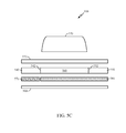
It will be appreciated that various aspects disclosed herein can be described as functional equivalents to the structures, materials and/or devices described and/or recognized by those skilled in the art. For example, in one aspect, a package tracking label (e.g., package tracking label 100 in FIGS. 1-3 and package tracking label 500 in FIGS. 5A-C ) may comprise an adhesive layer (e.g., adhesive layer 180 in FIG. 2 and the second adhesive layer 580 in FIG. 5C ); a removable cover (e.g., removable cover 190 in FIG. 2 and backer 590 in FIG. 5C ) on a first side of the adhesive layer; a substrate (e.g., substrate 160 in FIG. 2 and flex board 560 in FIG. 5C ) on a second side of the adhesive layer opposite the first side of the adhesive layer; means for transmitting a signal (e.g., antenna circuit 101 in FIG. 1 ) on the substrate; a mold layer (e.g., mold layer 170 in FIG. 2 and encapsulation layer 570 in FIG. 5C ) on the substrate configured to encapsulate the means for transmitting the signal; means for activation (e.g., activation tab 140 in FIGS. 1 and 2 and activation tab 540 in FIGS. 5A and 5C ) on the mold layer configured to activate the means for transmitting the signal upon removal; and means for deactivation (e.g., deactivation tab 150 in FIGS. 1-3 and deactivation tab 550 in FIGS. 5A-5C ) on the mold layer configured to deactivate the means for transmitting the signal upon removal. It will be appreciated that the aforementioned aspects are merely provided as examples and the various aspects claimed are not limited to the specific references and/or illustrations cited as examples.
One or more of the components, processes, features, and/or functions illustrated in FIGS. 1-5C may be rearranged and/or combined into a single component, process, feature or function or incorporated in several components, processes, or functions. Additional elements, components, processes, and/or functions may also be added without departing from the disclosure. It should also be noted that FIGS. 1-5C and its corresponding description in the present disclosure is not limited to dies and/or ICs. In some implementations, FIGS. 1-5C and its corresponding description may be used to manufacture, create, provide, and/or produce integrated devices. In some implementations, a device may include a die, an integrated device, a die package, an integrated circuit (IC), a device package, an integrated circuit (IC) package, a wafer, a semiconductor device, a package on package (PoP) device, and/or an interposer.
The word “exemplary” is used herein to mean “serving as an example, instance, or illustration.” Any details described herein as “exemplary” is not to be construed as advantageous over other examples. Likewise, the term “examples” does not mean that all examples include the discussed feature, advantage or mode of operation. Furthermore, a particular feature and/or structure can be combined with one or more other features and/or structures. Moreover, at least a portion of the apparatus described hereby can be configured to perform at least a portion of a method described hereby.
The terminology used herein is for the purpose of describing particular examples and is not intended to be limiting of examples of the disclosure. As used herein, the singular forms “a,” “an,” and “the” are intended to include the plural forms as well, unless the context clearly indicates otherwise. It will be further understood that the terms “comprises”, “comprising,” “includes,” and/or “including,” when used herein, specify the presence of stated features, integers, actions, operations, elements, and/or components, but do not preclude the presence or addition of one or more other features, integers, actions, operations, elements, components, and/or groups thereof.
It should be noted that the terms “connected,” “coupled,” or any variant thereof, mean any connection or coupling, either direct or indirect, between elements, and can encompass a presence of an intermediate element between two elements that are “connected” or “coupled” together via the intermediate element.
Any reference herein to an element using a designation such as “first,” “second,” and so forth does not limit the quantity and/or order of those elements. Rather, these designations are used as a convenient method of distinguishing between two or more elements and/or instances of an element. Also, unless stated otherwise, a set of elements can comprise one or more elements.
Nothing stated or illustrated depicted in this application is intended to dedicate any component, action, feature, benefit, advantage, or equivalent to the public, regardless of whether the component, action, feature, benefit, advantage, or the equivalent is recited in the claims.
Further, those of skill in the art will appreciate that the various illustrative logical blocks, modules, circuits, and algorithm actions described in connection with the examples disclosed herein may be implemented as electronic hardware, computer software, or combinations of both. To clearly illustrate this interchangeability of hardware and software, various illustrative components, blocks, modules, circuits, and actions have been described above generally in terms of their functionality. Whether such functionality is implemented as hardware or software depends upon the particular application and design constraints imposed on the overall system. Skilled artisans may implement the described functionality in varying ways for each particular application, but such implementation decisions should not be interpreted as causing a departure from the scope of the present disclosure.
The methods, sequences and/or algorithms described in connection with the examples disclosed herein may be incorporated directly in hardware, in a software module executed by a processor, or in a combination of the two. A software module may reside in RAM memory, flash memory, ROM memory, EPROM memory, EEPROM memory, registers, or any other form of storage medium known in the art. An exemplary storage medium is coupled to the processor such that the processor can read information from, and write information to, the storage medium. In the alternative, the storage medium may be integral to the processor.
The various illustrative logical blocks, modules, and circuits described in connection with the aspects disclosed herein may be implemented or performed with a general purpose processor, a digital signal processor (DSP), an application specific integrated circuit (ASIC), a field programmable gate array (FPGA) or other programmable logic device, discrete gate or transistor logic, discrete hardware components, or any combination thereof designed to perform the functions described herein. A general purpose processor may be a microprocessor, but in the alternative, the processor may be any conventional processor, controller, microcontroller, or state machine. A processor may also be implemented as a combination of computing devices (e.g., a combination of a DSP and a microprocessor, a plurality of microprocessors, one or more microprocessors in conjunction with a DSP core, or any other such configuration).
Although some aspects have been described in connection with a device, it goes without saying that these aspects also constitute a description of the corresponding method, and so a block or a component of a device should also be understood as a corresponding method action or as a feature of a method action. Analogously thereto, aspects described in connection with or as a method action also constitute a description of a corresponding block or detail or feature of a corresponding device. Some or all of the method actions can be performed by a hardware apparatus (or using a hardware apparatus), such as, for example, a microprocessor, a programmable computer or an electronic circuit. In some examples, some or a plurality of the most important method actions can be performed by such an apparatus.
In the detailed description above it can be seen that different features are grouped together in examples. This manner of disclosure should not be understood as an intention that the claimed examples have more features than are explicitly mentioned in the respective claim. Rather, the disclosure may include fewer than all features of an individual example disclosed. Therefore, the following claims should hereby be deemed to be incorporated in the description, wherein each claim by itself can stand as a separate example. Although each claim by itself can stand as a separate example, it should be noted that—although a dependent claim can refer in the claims to a specific combination with one or a plurality of claims—other examples can also encompass or include a combination of said dependent claim with the subject matter of any other dependent claim or a combination of any feature with other dependent and independent claims. Such combinations are proposed herein, unless it is explicitly expressed that a specific combination is not intended. Furthermore, it is also intended that features of a claim can be included in any other independent claim, even if said claim is not directly dependent on the independent claim.
It should furthermore be noted that methods, systems, and apparatus disclosed in the description or in the claims can be implemented by a device comprising means for performing the respective actions of this method.
Furthermore, in some examples, an individual action can be subdivided into a plurality of sub-actions or contain a plurality of sub-actions. Such sub-actions can be contained in the disclosure of the individual action and be part of the disclosure of the individual action.
While the foregoing disclosure shows illustrative examples of the disclosure, it should be noted that various changes and modifications could be made herein without departing from the scope of the disclosure as defined by the appended claims. The functions and/or actions of the method claims in accordance with the examples of the disclosure described herein need not be performed in any particular order. Additionally, well-known elements will not be described in detail or may be omitted so as to not obscure the relevant details of the aspects and examples disclosed herein. Furthermore, although elements of the disclosure may be described or claimed in the singular, the plural is contemplated unless limitation to the singular is explicitly stated.
Claims (28)
1. A package tracking label, comprising:
an adhesive layer;
a removable cover on a first side of the adhesive layer;
a substrate on a second side of the adhesive layer opposite the first side of the adhesive layer;
an antenna circuit on the substrate;
a mold layer on the substrate configured to encapsulate the antenna circuit;
an activation tab on the substrate configured to activate the antenna circuit upon removal; and
a deactivation tab on the substrate configured to deactivate the antenna circuit upon removal.
2. The package tracking label of claim 1 , wherein the activation tab is connected to the removable cover and configured to be removed with the removal of the removable cover.
3. The package tracking label of claim 1 , wherein the antenna circuit is a Bluetooth Low Energy antenna circuit.
4. The package tracking label of claim 1 , wherein the antenna circuit comprises a battery, a microprocessor coupled to the battery, and an antenna coupled to the microprocessor.
5. The package tracking label of claim 4 , wherein the activation tab is configured to activate a first general purpose input output pin of the microprocessor that enables activation of the microprocessor.
6. The package tracking label of claim 5 , wherein the deactivation tab is configured to activate a second general purpose input output pin of the microprocessor that enables deactivation of the microprocessor.
7. The package tracking label of claim 6 , wherein the microprocessor is a Bluetooth Low Energy microprocessor configured to control operation of the antenna.
8. The package tracking label of claim 1 , wherein the substrate is one of a polyester substrate or a printed screen paper.
9. The package tracking label of claim 1 , wherein the deactivation tab is configured to be applied to a package such that the package cannot be opened without removal or breakage of the deactivation tab.
10. A package tracking label, comprising:
an adhesive layer;
a removable cover on a first side of the adhesive layer;
a substrate on a second side of the adhesive layer opposite the first side of the adhesive layer;
means for transmitting a signal on the substrate;
a mold layer on the substrate configured to encapsulate the means for transmitting the signal;
means for activation on the substrate configured to activate the means for transmitting the signal upon removal; and
means for deactivation on the substrate configured to deactivate the means for transmitting the signal upon removal.
11. The package tracking label of claim 10 , wherein the means for activation is connected to the removable cover and configured to be removed with the removal of the removable cover.
12. The package tracking label of claim 10 , wherein the means for transmitting the signal is a Bluetooth Low Energy antenna circuit.
13. The package tracking label of claim 10 , wherein the means for transmitting the signal comprises a battery, a microprocessor coupled to the battery, and an antenna coupled to the microprocessor.
14. The package tracking label of claim 13 , wherein the means for activation is configured to activate a first general purpose input output pin of the microprocessor that enables activation of the microprocessor.
15. The package tracking label of claim 14 , wherein the means for deactivation is configured to activate a second general purpose input output pin of the microprocessor that enables deactivation of the microprocessor.
16. The package tracking label of claim 15 , wherein the microprocessor is a Bluetooth Low Energy microprocessor configured to control operation of the antenna.
17. The package tracking label of claim 10 , wherein the substrate is one of a polyester substrate or a printed screen paper.
18. A method of tracking a package, comprising:
applying a package label to a package, the package label comprises an antenna circuit, an activation tab configured to activate the antenna circuit, and a deactivation tab configured to deactivate the antenna circuit;
activating the antenna circuit by removing the activation tab;
periodically transmitting a signal by the antenna circuit upon activation, the signal comprises information that identifies the package; and
receiving the signal and using the information in the signal to track a location of the package.
19. The method of claim 18 , further comprising deactivating the antenna circuit by removing the deactivation tab.
20. The method of claim 18 , wherein the signal is a Bluetooth Low Energy signal.
21. The method of claim 18 , wherein the activation tab is connected to a removable cover and configured to be removed with the removal of the removable cover.
22. The method of claim 18 , wherein the antenna circuit comprises a battery, a microprocessor coupled to the battery, and an antenna coupled to the microprocessor.
23. The method of claim 18 , wherein the activation tab is configured to activate a first general purpose input output pin of a microprocessor that enables activation of the microprocessor.
24. The method of claim 18 , wherein the deactivation tab is configured to activate a second general purpose input output pin of a microprocessor that enables deactivation of the microprocessor.
25. The method of claim 18 , wherein the deactivation tab is configured to be applied to a package such that the package cannot be opened without removal or breakage of the deactivation tab.
26. A non-transitory computer-readable medium comprising instructions that when executed by a processor cause the processor to perform a method comprising:
activating an antenna circuit when an activation tab configured to activate the antenna circuit is removed;
periodically transmitting a signal by the antenna circuit upon activation, the signal comprises information that identifies a package;
receiving the signal and using the information in the signal to track a location of the package; and
deactivating the antenna circuit when a deactivation tab configured to deactivate the antenna circuit is removed.
27. The non-transitory computer-readable medium of claim 26 , wherein the signal is a Bluetooth Low Energy signal.
28. The non-transitory computer-readable medium of claim 26 , wherein the activation tab is configured to activate a first general purpose input output pin of the processor that enables activation of the processor.
Priority Applications (4)
| Application Number | Priority Date | Filing Date | Title |
|---|---|---|---|
| US15/839,847 US10108898B1 (en) | 2017-09-14 | 2017-12-12 | Package tracking label having activation and deactivation tabs |
| PCT/US2018/046450 WO2019055161A1 (en) | 2017-09-14 | 2018-08-13 | Package tracking label |
| CN201880058718.2A CN111066035A (en) | 2017-09-14 | 2018-08-13 | Parcel tracking label |
| EP18762966.2A EP3682375B1 (en) | 2017-09-14 | 2018-08-13 | Package tracking label |
Applications Claiming Priority (2)
| Application Number | Priority Date | Filing Date | Title |
|---|---|---|---|
| US201762558843P | 2017-09-14 | 2017-09-14 | |
| US15/839,847 US10108898B1 (en) | 2017-09-14 | 2017-12-12 | Package tracking label having activation and deactivation tabs |
Publications (1)
| Publication Number | Publication Date |
|---|---|
| US10108898B1 true US10108898B1 (en) | 2018-10-23 |
Family
ID=63833372
Family Applications (1)
| Application Number | Title | Priority Date | Filing Date |
|---|---|---|---|
| US15/839,847 Active US10108898B1 (en) | 2017-09-14 | 2017-12-12 | Package tracking label having activation and deactivation tabs |
Country Status (4)
| Country | Link |
|---|---|
| US (1) | US10108898B1 (en) |
| EP (1) | EP3682375B1 (en) |
| CN (1) | CN111066035A (en) |
| WO (1) | WO2019055161A1 (en) |
Cited By (4)
| Publication number | Priority date | Publication date | Assignee | Title |
|---|---|---|---|---|
| US10964197B2 (en) | 2018-10-09 | 2021-03-30 | Reelables, Inc. | Low-power electronic tape for tracking items |
| US20220012685A1 (en) * | 2018-11-23 | 2022-01-13 | Pa. Cotte Sa | System for routing objects with simplified routing cycle initiation |
| US20220027698A1 (en) * | 2020-07-24 | 2022-01-27 | Trackonomy Systems, Inc. | Tearing to turn on wireless node with multiple cutouts for re-use |
| WO2022157092A1 (en) * | 2021-01-21 | 2022-07-28 | Protektorwerk Florenz Maisch Gmbh & Co. Kg | System and method for capturing locations of installment of building products |
Families Citing this family (1)
| Publication number | Priority date | Publication date | Assignee | Title |
|---|---|---|---|---|
| WO2021174158A1 (en) * | 2020-02-27 | 2021-09-02 | GANTON, Robert, Bruce | System and apparatus for generating dynamic reference voltage in power constrained devices |
Citations (9)
| Publication number | Priority date | Publication date | Assignee | Title |
|---|---|---|---|---|
| US6465880B1 (en) * | 1997-08-28 | 2002-10-15 | Nippon Telegraph And Telephone Corporation | IC card indicating state of usage and system therefor |
| US7215976B2 (en) | 2001-11-30 | 2007-05-08 | Symbol Technologies, Inc. | RFID device, system and method of operation including a hybrid backscatter-based RFID tag protocol compatible with RFID, bluetooth and/or IEEE 802.11x infrastructure |
| US7893839B2 (en) | 2005-11-23 | 2011-02-22 | Avery Dennison Corporation | Deactivatable RFID labels and tags and methods of making same |
| US20130021215A1 (en) | 2010-01-26 | 2013-01-24 | Takahiro Suzuki | Injection molded and in-mold decorated article with antenna, method for producing the same, and power-feeding sturcture of casing with antenna |
| US9471817B1 (en) * | 2015-07-09 | 2016-10-18 | Raed H. AlHazme | Action-triggered radio-frequency identification tag |
| US20160371517A1 (en) * | 2015-06-16 | 2016-12-22 | Motorola Mobility Llc | Person-Centric Activation of Radio Frequency Identification (RFID) Tag |
| US20170229000A1 (en) | 2014-08-04 | 2017-08-10 | Avery Dennison Corporation | Time-Temperature Tracking Label |
| US9754137B2 (en) | 2015-06-16 | 2017-09-05 | Motorola Mobility Llc | On-demand activation of radio frequency identification (RFID) tag |
| US20180025603A1 (en) * | 2016-07-20 | 2018-01-25 | United Parcel Service Of America, Inc. | Location tracking using beacons |
Family Cites Families (2)
| Publication number | Priority date | Publication date | Assignee | Title |
|---|---|---|---|---|
| US6073856A (en) * | 1997-09-05 | 2000-06-13 | Dai Nippon Printing Co., Ltd. | Noncontact IC device |
| US7151455B2 (en) * | 2004-04-30 | 2006-12-19 | Kimberly-Clark Worldwide, Inc. | Activating a data tag by load or orientation or user control |
-
2017
- 2017-12-12 US US15/839,847 patent/US10108898B1/en active Active
-
2018
- 2018-08-13 EP EP18762966.2A patent/EP3682375B1/en active Active
- 2018-08-13 WO PCT/US2018/046450 patent/WO2019055161A1/en unknown
- 2018-08-13 CN CN201880058718.2A patent/CN111066035A/en active Pending
Patent Citations (9)
| Publication number | Priority date | Publication date | Assignee | Title |
|---|---|---|---|---|
| US6465880B1 (en) * | 1997-08-28 | 2002-10-15 | Nippon Telegraph And Telephone Corporation | IC card indicating state of usage and system therefor |
| US7215976B2 (en) | 2001-11-30 | 2007-05-08 | Symbol Technologies, Inc. | RFID device, system and method of operation including a hybrid backscatter-based RFID tag protocol compatible with RFID, bluetooth and/or IEEE 802.11x infrastructure |
| US7893839B2 (en) | 2005-11-23 | 2011-02-22 | Avery Dennison Corporation | Deactivatable RFID labels and tags and methods of making same |
| US20130021215A1 (en) | 2010-01-26 | 2013-01-24 | Takahiro Suzuki | Injection molded and in-mold decorated article with antenna, method for producing the same, and power-feeding sturcture of casing with antenna |
| US20170229000A1 (en) | 2014-08-04 | 2017-08-10 | Avery Dennison Corporation | Time-Temperature Tracking Label |
| US20160371517A1 (en) * | 2015-06-16 | 2016-12-22 | Motorola Mobility Llc | Person-Centric Activation of Radio Frequency Identification (RFID) Tag |
| US9754137B2 (en) | 2015-06-16 | 2017-09-05 | Motorola Mobility Llc | On-demand activation of radio frequency identification (RFID) tag |
| US9471817B1 (en) * | 2015-07-09 | 2016-10-18 | Raed H. AlHazme | Action-triggered radio-frequency identification tag |
| US20180025603A1 (en) * | 2016-07-20 | 2018-01-25 | United Parcel Service Of America, Inc. | Location tracking using beacons |
Cited By (6)
| Publication number | Priority date | Publication date | Assignee | Title |
|---|---|---|---|---|
| US10964197B2 (en) | 2018-10-09 | 2021-03-30 | Reelables, Inc. | Low-power electronic tape for tracking items |
| US11594120B2 (en) | 2018-10-09 | 2023-02-28 | Reelables, Inc. | Low-power electronic tape for tracking items |
| US20220012685A1 (en) * | 2018-11-23 | 2022-01-13 | Pa. Cotte Sa | System for routing objects with simplified routing cycle initiation |
| US20220027698A1 (en) * | 2020-07-24 | 2022-01-27 | Trackonomy Systems, Inc. | Tearing to turn on wireless node with multiple cutouts for re-use |
| US11900195B2 (en) * | 2020-07-24 | 2024-02-13 | Trackonomy Systems, Inc. | Tearing to turn on wireless node with multiple cutouts for re-use |
| WO2022157092A1 (en) * | 2021-01-21 | 2022-07-28 | Protektorwerk Florenz Maisch Gmbh & Co. Kg | System and method for capturing locations of installment of building products |
Also Published As
| Publication number | Publication date |
|---|---|
| EP3682375A1 (en) | 2020-07-22 |
| WO2019055161A1 (en) | 2019-03-21 |
| EP3682375B1 (en) | 2021-07-07 |
| CN111066035A (en) | 2020-04-24 |
Similar Documents
| Publication | Publication Date | Title |
|---|---|---|
| US10108898B1 (en) | Package tracking label having activation and deactivation tabs | |
| US7843341B2 (en) | Label with electronic components and method of making same | |
| US8833664B2 (en) | Enhanced performance and security RFID device | |
| EP2960834B1 (en) | Container | |
| JP2002308437A (en) | Inspection system using rfid tag | |
| KR101245366B1 (en) | Splitting label tag | |
| US11537836B2 (en) | Merchandise attachment with RFID transponder | |
| US8742928B2 (en) | Integrated document holder and RFID tag | |
| CN106557805A (en) | Safe wireless radio frequency recognition volume label, system and method | |
| US7951451B2 (en) | Self-adhesive document incorporating a radiofrequency identification device | |
| CN104794510A (en) | Recyclable electronic tag and logistics courier receipt with same | |
| CN205451142U (en) | A RFID electronic tags and commodity circulation parcel for commodity circulation parcel | |
| JP2002352199A (en) | Wrist-worn type antenna for rfid tag communication | |
| CN108091245B (en) | Logistics adhesive label with RFID function and use method thereof | |
| CN210199804U (en) | Prevent breakable electronic tags who shifts | |
| JP2020027126A (en) | Neck hanging label | |
| JP2009259075A (en) | Rfid tag-equipped label | |
| TW202009780A (en) | Package tracking label | |
| US8289168B2 (en) | RFID anti-theft tag structure | |
| CN218825555U (en) | Novel double-frequency anti-counterfeiting electronic tag | |
| CN214751949U (en) | Flexible anti-fake anti-metal ultrahigh frequency RFID (radio frequency identification) label | |
| CN108320015B (en) | Ultrahigh frequency RFID (radio frequency identification device) anti-tearing label | |
| JP2002225462A (en) | Non-contact ic slip and method for using the same | |
| CN104933462A (en) | Fragile label for vehicle lamp | |
| KR20070061029A (en) | Label waybill integrated radio frequency identification tag for home-delivery reuseable |
Legal Events
| Date | Code | Title | Description |
|---|---|---|---|
| FEPP | Fee payment procedure |
Free format text: ENTITY STATUS SET TO UNDISCOUNTED (ORIGINAL EVENT CODE: BIG.); ENTITY STATUS OF PATENT OWNER: LARGE ENTITY |
|
| STCF | Information on status: patent grant |
Free format text: PATENTED CASE |
|
| MAFP | Maintenance fee payment |
Free format text: PAYMENT OF MAINTENANCE FEE, 4TH YEAR, LARGE ENTITY (ORIGINAL EVENT CODE: M1551); ENTITY STATUS OF PATENT OWNER: LARGE ENTITY Year of fee payment: 4 |