US10096784B2 - Compound for organic optoelectric device, composition for organic optoelectric device and organic optoelectric device and display device - Google Patents
Compound for organic optoelectric device, composition for organic optoelectric device and organic optoelectric device and display device Download PDFInfo
- Publication number
- US10096784B2 US10096784B2 US15/677,491 US201715677491A US10096784B2 US 10096784 B2 US10096784 B2 US 10096784B2 US 201715677491 A US201715677491 A US 201715677491A US 10096784 B2 US10096784 B2 US 10096784B2
- Authority
- US
- United States
- Prior art keywords
- group
- substituted
- unsubstituted
- compound
- optoelectric device
- Prior art date
- Legal status (The legal status is an assumption and is not a legal conclusion. Google has not performed a legal analysis and makes no representation as to the accuracy of the status listed.)
- Active
Links
- 0 *c1nc(-c2ccccc2)nc(-c2ccccc2)n1 Chemical compound *c1nc(-c2ccccc2)nc(-c2ccccc2)n1 0.000 description 44
- YYARJHFQUGAVDD-UHFFFAOYSA-N C1=CC(C2=CC=CC3=C2C=CC=C3)=CC(N2C3=C(C=CC=C3)C3=C2C2=C(C4=C(C=CC=C4)S2)C2=C3C3=C(C=CC=C3)C3=C2C=CC=C3)=C1.C1=CC2=C(C=C1)C(C1=CC=C(N3C4=C(C=CC=C4)C4=C3C3=C(C5=C(C=CC=C5)S3)C3=C4C4=C(C=CC=C4)C4=C3C=CC=C4)C=C1)=CC=C2.C1=CC2=CC=C(C3=CC(N4C5=C(C=CC=C5)C5=C4C4=C(C6=C(C=CC=C6)S4)C4=C5C5=C(C=CC=C5)C5=C4C=CC=C5)=CC=C3)C=C2C=C1 Chemical compound C1=CC(C2=CC=CC3=C2C=CC=C3)=CC(N2C3=C(C=CC=C3)C3=C2C2=C(C4=C(C=CC=C4)S2)C2=C3C3=C(C=CC=C3)C3=C2C=CC=C3)=C1.C1=CC2=C(C=C1)C(C1=CC=C(N3C4=C(C=CC=C4)C4=C3C3=C(C5=C(C=CC=C5)S3)C3=C4C4=C(C=CC=C4)C4=C3C=CC=C4)C=C1)=CC=C2.C1=CC2=CC=C(C3=CC(N4C5=C(C=CC=C5)C5=C4C4=C(C6=C(C=CC=C6)S4)C4=C5C5=C(C=CC=C5)C5=C4C=CC=C5)=CC=C3)C=C2C=C1 YYARJHFQUGAVDD-UHFFFAOYSA-N 0.000 description 2
- IHHPCFQSOLDHHF-UHFFFAOYSA-N C1=CC(N2C3=C(C=CC=C3)C3=C2C2=C(C4=C(C=CC=C4)O2)C2=C3C3=C(C=CC=C3)C3=C2C=CC=C3)=CC(C2=CC3=C(C=C2)C2=C(C=CC=C2)S3)=C1.C1=CC(N2C3=C(C=CC=C3)C3=C2C2=C(C4=C(C=CC=C4)O2)C2=C3C3=C(C=CC=C3)C3=C2C=CC=C3)=CC(C2=CC3=C(C=C2)SC2=C3C=CC=C2)=C1.C1=CC2=C(C=C1)C1=C(O2)C2=C(C3=C(C=CC=C3)N2C2=CC=C(C3=CC4=C(C=C3)C3=C(C=CC=C3)S4)C=C2)C2=C1C1=C(C=CC=C1)C1=C2C=CC=C1 Chemical compound C1=CC(N2C3=C(C=CC=C3)C3=C2C2=C(C4=C(C=CC=C4)O2)C2=C3C3=C(C=CC=C3)C3=C2C=CC=C3)=CC(C2=CC3=C(C=C2)C2=C(C=CC=C2)S3)=C1.C1=CC(N2C3=C(C=CC=C3)C3=C2C2=C(C4=C(C=CC=C4)O2)C2=C3C3=C(C=CC=C3)C3=C2C=CC=C3)=CC(C2=CC3=C(C=C2)SC2=C3C=CC=C2)=C1.C1=CC2=C(C=C1)C1=C(O2)C2=C(C3=C(C=CC=C3)N2C2=CC=C(C3=CC4=C(C=C3)C3=C(C=CC=C3)S4)C=C2)C2=C1C1=C(C=CC=C1)C1=C2C=CC=C1 IHHPCFQSOLDHHF-UHFFFAOYSA-N 0.000 description 2
- LPXARJAHCXWZMN-UHFFFAOYSA-N C1=CC(N2C3=C(C=CC=C3)C3=C2C2=C(C4=C(C=CC=C4)O2)C2=C3C3=C(C=CC=C3)C3=C2C=CC=C3)=CC(C2=CC=C3C4=C(C=CC=C4)/C4=C/C=C\C2=C34)=C1.C1=CC2=C(C=C1)C1=C(O2)C2=C(C3=C(C=CC=C3)N2C2=CC=C3C4=C(C=CC=C4)/C4=C/C=C\C2=C34)C2=C1C1=C(C=CC=C1)C1=C2C=CC=C1.C1=CC=C(C2(C3=CC=CC=C3)C3=C(C=CC=C3)C3=C2C=C(N2C4=C(C=CC=C4)C4=C2C2=C(C5=C(C=CC=C5)O2)C2=C4C4=C(C=CC=C4)C4=C2C=CC=C4)C=C3)C=C1 Chemical compound C1=CC(N2C3=C(C=CC=C3)C3=C2C2=C(C4=C(C=CC=C4)O2)C2=C3C3=C(C=CC=C3)C3=C2C=CC=C3)=CC(C2=CC=C3C4=C(C=CC=C4)/C4=C/C=C\C2=C34)=C1.C1=CC2=C(C=C1)C1=C(O2)C2=C(C3=C(C=CC=C3)N2C2=CC=C3C4=C(C=CC=C4)/C4=C/C=C\C2=C34)C2=C1C1=C(C=CC=C1)C1=C2C=CC=C1.C1=CC=C(C2(C3=CC=CC=C3)C3=C(C=CC=C3)C3=C2C=C(N2C4=C(C=CC=C4)C4=C2C2=C(C5=C(C=CC=C5)O2)C2=C4C4=C(C=CC=C4)C4=C2C=CC=C4)C=C3)C=C1 LPXARJAHCXWZMN-UHFFFAOYSA-N 0.000 description 2
- NBJJWMUNNJUCGC-UHFFFAOYSA-N C1=CC(N2C3=C(C=CC=C3)C3=C2C2=C(C4=C(C=CC=C4)S2)C2=C3C3=C(C=CC=C3)C3=C2C=CC=C3)=CC(C2=CC3=C(C=C2)OC2=C3C=CC=C2)=C1.C1=CC(N2C3=C(C=CC=C3)C3=C2C2=C(C4=C(C=CC=C4)S2)C2=C3C3=C(C=CC=C3)C3=C2C=CC=C3)=CC(C2=CC=CC3=C2OC2=C3C=CC=C2)=C1.C1=CC2=C(C=C1)C1=C(C=CC(C3=CC=C(N4C5=C(C=CC=C5)C5=C4C4=C(C6=C(C=CC=C6)S4)C4=C5C5=C(C=CC=C5)C5=C4C=CC=C5)C=C3)=C1)O2 Chemical compound C1=CC(N2C3=C(C=CC=C3)C3=C2C2=C(C4=C(C=CC=C4)S2)C2=C3C3=C(C=CC=C3)C3=C2C=CC=C3)=CC(C2=CC3=C(C=C2)OC2=C3C=CC=C2)=C1.C1=CC(N2C3=C(C=CC=C3)C3=C2C2=C(C4=C(C=CC=C4)S2)C2=C3C3=C(C=CC=C3)C3=C2C=CC=C3)=CC(C2=CC=CC3=C2OC2=C3C=CC=C2)=C1.C1=CC2=C(C=C1)C1=C(C=CC(C3=CC=C(N4C5=C(C=CC=C5)C5=C4C4=C(C6=C(C=CC=C6)S4)C4=C5C5=C(C=CC=C5)C5=C4C=CC=C5)C=C3)=C1)O2 NBJJWMUNNJUCGC-UHFFFAOYSA-N 0.000 description 2
- SUDLOONJRNSLCB-UHFFFAOYSA-N C1=CC(N2C3=C(C=CC=C3)C3=C2C2=C(C4=C(C=CC=C4)S2)C2=C3C3=C(C=CC=C3)C3=C2C=CC=C3)=CC(C2=CC=CC3=C2C2=C(C=CC=C2)O3)=C1.C1=CC2=C(C=C1)C1=C(C=CC=C1C1=CC=C(N3C4=C(C=CC=C4)C4=C3C3=C(C5=C(C=CC=C5)S3)C3=C4C4=C(C=CC=C4)C4=C3C=CC=C4)C=C1)O2.C1=CC2=C(C=C1)C1=C(O2)C(C2=CC=C(N3C4=C(C=CC=C4)C4=C3C3=C(C5=C(C=CC=C5)S3)C3=C4C4=C(C=CC=C4)C4=C3C=CC=C4)C=C2)=CC=C1 Chemical compound C1=CC(N2C3=C(C=CC=C3)C3=C2C2=C(C4=C(C=CC=C4)S2)C2=C3C3=C(C=CC=C3)C3=C2C=CC=C3)=CC(C2=CC=CC3=C2C2=C(C=CC=C2)O3)=C1.C1=CC2=C(C=C1)C1=C(C=CC=C1C1=CC=C(N3C4=C(C=CC=C4)C4=C3C3=C(C5=C(C=CC=C5)S3)C3=C4C4=C(C=CC=C4)C4=C3C=CC=C4)C=C1)O2.C1=CC2=C(C=C1)C1=C(O2)C(C2=CC=C(N3C4=C(C=CC=C4)C4=C3C3=C(C5=C(C=CC=C5)S3)C3=C4C4=C(C=CC=C4)C4=C3C=CC=C4)C=C2)=CC=C1 SUDLOONJRNSLCB-UHFFFAOYSA-N 0.000 description 2
- TVHVQVJEHDBICV-UHFFFAOYSA-N C1=CC(N2C3=C(C=CC=C3)C3=C2C=CC=C3)=CC(N2C3=C(C=CC=C3)C3=C2C2=C(C4=C(C=CC=C4)S2)C2=C3C3=C(C=CC=C3)C3=C2C=CC=C3)=C1.C1=CC2=C(C=C1)C1=C(C=CC(N3C4=C(C=CC=C4)C4=C3C3=C(C5=C(C=CC=C5)S3)C3=C4C4=C(C=CC=C4)C4=C3C=CC=C4)=C1)S2.C1=CC2=C(C=C1)C1=C(S2)C2=C(C3=C(C=CC=C3)N2C2=CC=C(N3C4=C(C=CC=C4)C4=C3C=CC=C4)C=C2)C2=C1C1=C(C=CC=C1)C1=C2C=CC=C1 Chemical compound C1=CC(N2C3=C(C=CC=C3)C3=C2C=CC=C3)=CC(N2C3=C(C=CC=C3)C3=C2C2=C(C4=C(C=CC=C4)S2)C2=C3C3=C(C=CC=C3)C3=C2C=CC=C3)=C1.C1=CC2=C(C=C1)C1=C(C=CC(N3C4=C(C=CC=C4)C4=C3C3=C(C5=C(C=CC=C5)S3)C3=C4C4=C(C=CC=C4)C4=C3C=CC=C4)=C1)S2.C1=CC2=C(C=C1)C1=C(S2)C2=C(C3=C(C=CC=C3)N2C2=CC=C(N3C4=C(C=CC=C4)C4=C3C=CC=C4)C=C2)C2=C1C1=C(C=CC=C1)C1=C2C=CC=C1 TVHVQVJEHDBICV-UHFFFAOYSA-N 0.000 description 2
- ZFWGKWNRWNFJJX-UHFFFAOYSA-N C1=CC2=C(C=C1)C(N1C3=C(C=CC=C3)C3=C1C1=C(C4=C(C=CC=C4)S1)C1=C3C3=C(C=CC=C3)C3=C1C=CC=C3)=CC=C2.C1=CC2=C(C=C1)C1=C(C=C2)C=C(N2C3=C(C=CC=C3)C3=C2C2=C(C4=C(C=CC=C4)S2)C2=C3C3=C(C=CC=C3)C3=C2C=CC=C3)C=C1.C1=CC2=C(C=C1)C=C(N1C3=C(C=CC=C3)C3=C1C1=C(C4=C(C=CC=C4)S1)C1=C3C3=C(C=CC=C3)C3=C1C=CC=C3)C=C2 Chemical compound C1=CC2=C(C=C1)C(N1C3=C(C=CC=C3)C3=C1C1=C(C4=C(C=CC=C4)S1)C1=C3C3=C(C=CC=C3)C3=C1C=CC=C3)=CC=C2.C1=CC2=C(C=C1)C1=C(C=C2)C=C(N2C3=C(C=CC=C3)C3=C2C2=C(C4=C(C=CC=C4)S2)C2=C3C3=C(C=CC=C3)C3=C2C=CC=C3)C=C1.C1=CC2=C(C=C1)C=C(N1C3=C(C=CC=C3)C3=C1C1=C(C4=C(C=CC=C4)S1)C1=C3C3=C(C=CC=C3)C3=C1C=CC=C3)C=C2 ZFWGKWNRWNFJJX-UHFFFAOYSA-N 0.000 description 2
- BRNUWPFUCQMQLG-UHFFFAOYSA-N C1=CC2=C(C=C1)C1=C(C=CC(N3C4=C(C=CC=C4)C4=C3C3=C(C5=C(C=CC=C5)O3)C3=C4C4=C(C=CC=C4)C4=C3C=CC=C4)=C1)O2.C1=CC=C(N2C3=C(C=CC=C3)C3=C2C(C2=CC=C(N4C5=C(C=CC=C5)C5=C4C4=C(C6=C(C=CC=C6)O4)C4=C5C5=C(C=CC=C5)C5=C4C=CC=C5)C=C2)=CC=C3)C=C1.C1=CC=C(N2C3=C(C=CC=C3)C3=C2C(C2=CC=CC(N4C5=C(C=CC=C5)C5=C4C4=C(C6=C(C=CC=C6)O4)C4=C5C5=C(C=CC=C5)C5=C4C=CC=C5)=C2)=CC=C3)C=C1 Chemical compound C1=CC2=C(C=C1)C1=C(C=CC(N3C4=C(C=CC=C4)C4=C3C3=C(C5=C(C=CC=C5)O3)C3=C4C4=C(C=CC=C4)C4=C3C=CC=C4)=C1)O2.C1=CC=C(N2C3=C(C=CC=C3)C3=C2C(C2=CC=C(N4C5=C(C=CC=C5)C5=C4C4=C(C6=C(C=CC=C6)O4)C4=C5C5=C(C=CC=C5)C5=C4C=CC=C5)C=C2)=CC=C3)C=C1.C1=CC=C(N2C3=C(C=CC=C3)C3=C2C(C2=CC=CC(N4C5=C(C=CC=C5)C5=C4C4=C(C6=C(C=CC=C6)O4)C4=C5C5=C(C=CC=C5)C5=C4C=CC=C5)=C2)=CC=C3)C=C1 BRNUWPFUCQMQLG-UHFFFAOYSA-N 0.000 description 2
- UGWILGPIQPREOU-UHFFFAOYSA-N C1=CC2=C(C=C1)C1=C(C=CC(N3C4=C(C=CC=C4)C4=C3C3=C(C5=C(C=CC=C5)S3)C3=C4C4=C(C=CC=C4)C4=C3C=CC=C4)=C1)C=C2.C1=CC2=C(C=C1)C1=C(C=CC=C1)C(N1C3=C(C=CC=C3)C3=C1C1=C(C4=C(C=CC=C4)S1)C1=C3C3=C(C=CC=C3)C3=C1C=CC=C3)=C2.C1=CC2=C(C=C1)C1=C(S2)C2=C(C3=C(C=CC=C3)N2C2=CC3=C(C=C2)C2=C(C=CC=C2)C2=C3C=CC=C2)C2=C1C1=C(C=CC=C1)C1=C2C=CC=C1 Chemical compound C1=CC2=C(C=C1)C1=C(C=CC(N3C4=C(C=CC=C4)C4=C3C3=C(C5=C(C=CC=C5)S3)C3=C4C4=C(C=CC=C4)C4=C3C=CC=C4)=C1)C=C2.C1=CC2=C(C=C1)C1=C(C=CC=C1)C(N1C3=C(C=CC=C3)C3=C1C1=C(C4=C(C=CC=C4)S1)C1=C3C3=C(C=CC=C3)C3=C1C=CC=C3)=C2.C1=CC2=C(C=C1)C1=C(S2)C2=C(C3=C(C=CC=C3)N2C2=CC3=C(C=C2)C2=C(C=CC=C2)C2=C3C=CC=C2)C2=C1C1=C(C=CC=C1)C1=C2C=CC=C1 UGWILGPIQPREOU-UHFFFAOYSA-N 0.000 description 2
- DXHINGKWVOZUGT-UHFFFAOYSA-N C1=CC2=C(C=C1)C1=C(O2)C2=C(C3=C(C=CC=C3)N2C2=CC=C(C3=CC=C4C5=C(C=CC=C5)/C5=C/C=C\C3=C45)C=C2)C2=C1C1=C(C=CC=C1)C1=C2C=CC=C1.C1=CC=C(C2=C3C=CC=CC3=NC(N3C4=C(C=CC=C4)C4=C3C3=C(C5=C(C=CC=C5)O3)C3=C4C4=C(C=CC=C4)C4=C3C=CC=C4)=N2)C=C1.C1=CC=C(C2=CC=C(C3=C4C=CC=CC4=NC(N4C5=C(C=CC=C5)C5=C4C4=C(C6=C(C=CC=C6)O4)C4=C5C5=C(C=CC=C5)C5=C4C=CC=C5)=N3)C=C2)C=C1 Chemical compound C1=CC2=C(C=C1)C1=C(O2)C2=C(C3=C(C=CC=C3)N2C2=CC=C(C3=CC=C4C5=C(C=CC=C5)/C5=C/C=C\C3=C45)C=C2)C2=C1C1=C(C=CC=C1)C1=C2C=CC=C1.C1=CC=C(C2=C3C=CC=CC3=NC(N3C4=C(C=CC=C4)C4=C3C3=C(C5=C(C=CC=C5)O3)C3=C4C4=C(C=CC=C4)C4=C3C=CC=C4)=N2)C=C1.C1=CC=C(C2=CC=C(C3=C4C=CC=CC4=NC(N4C5=C(C=CC=C5)C5=C4C4=C(C6=C(C=CC=C6)O4)C4=C5C5=C(C=CC=C5)C5=C4C=CC=C5)=N3)C=C2)C=C1 DXHINGKWVOZUGT-UHFFFAOYSA-N 0.000 description 2
- FONOGPUWGJUUJG-UHFFFAOYSA-N C1=CC2=CC=CC(C3=C4C=CC=CC4=NC(N4C5=C(C=CC=C5)C5=C4C4=C(C6=C(C=CC=C6)O4)C4=C5C5=C(C=CC=C5)C5=C4C=CC=C5)=N3)=C2C=C1.C1=CC=C(C2=C(C3=C4C=CC=CC4=NC(N4C5=C(C=CC=C5)C5=C4C4=C(C6=C(C=CC=C6)O4)C4=C5C5=C(C=CC=C5)C5=C4C=CC=C5)=N3)C=CC=C2)C=C1.C1=CC=C(C2=CC(C3=C4C=CC=CC4=NC(N4C5=C(C=CC=C5)C5=C4C4=C(C6=C(C=CC=C6)O4)C4=C5C5=C(C=CC=C5)C5=C4C=CC=C5)=N3)=CC=C2)C=C1 Chemical compound C1=CC2=CC=CC(C3=C4C=CC=CC4=NC(N4C5=C(C=CC=C5)C5=C4C4=C(C6=C(C=CC=C6)O4)C4=C5C5=C(C=CC=C5)C5=C4C=CC=C5)=N3)=C2C=C1.C1=CC=C(C2=C(C3=C4C=CC=CC4=NC(N4C5=C(C=CC=C5)C5=C4C4=C(C6=C(C=CC=C6)O4)C4=C5C5=C(C=CC=C5)C5=C4C=CC=C5)=N3)C=CC=C2)C=C1.C1=CC=C(C2=CC(C3=C4C=CC=CC4=NC(N4C5=C(C=CC=C5)C5=C4C4=C(C6=C(C=CC=C6)O4)C4=C5C5=C(C=CC=C5)C5=C4C=CC=C5)=N3)=CC=C2)C=C1 FONOGPUWGJUUJG-UHFFFAOYSA-N 0.000 description 2
- YBNASIVBFRIXCF-UHFFFAOYSA-N C1=CC2=NC(N3C4=C(C=CC=C4)C4=C3C3=C(C5=C(C=CC=C5)O3)C3=C4C4=C(C=CC=C4)C4=C3C=CC=C4)=NC(C3=CC4=C(C=C3)C3=C(C=CC=C3)C=C4)=C2C=C1.C1=CC2=NC(N3C4=C(C=CC=C4)C4=C3C3=C(C5=C(C=CC=C5)O3)C3=C4C4=C(C=CC=C4)C4=C3C=CC=C4)=NC(C3=CC4=C(C=C3)C=CC3=C4C=CC=C3)=C2C=C1.C1=CC2=NC(N3C4=C(C=CC=C4)C4=C3C3=C(C5=C(C=CC=C5)O3)C3=C4C4=C(C=CC=C4)C4=C3C=CC=C4)=NC(C3=CC4=C(C=CC=C4)C=C3)=C2C=C1 Chemical compound C1=CC2=NC(N3C4=C(C=CC=C4)C4=C3C3=C(C5=C(C=CC=C5)O3)C3=C4C4=C(C=CC=C4)C4=C3C=CC=C4)=NC(C3=CC4=C(C=C3)C3=C(C=CC=C3)C=C4)=C2C=C1.C1=CC2=NC(N3C4=C(C=CC=C4)C4=C3C3=C(C5=C(C=CC=C5)O3)C3=C4C4=C(C=CC=C4)C4=C3C=CC=C4)=NC(C3=CC4=C(C=C3)C=CC3=C4C=CC=C3)=C2C=C1.C1=CC2=NC(N3C4=C(C=CC=C4)C4=C3C3=C(C5=C(C=CC=C5)O3)C3=C4C4=C(C=CC=C4)C4=C3C=CC=C4)=NC(C3=CC4=C(C=CC=C4)C=C3)=C2C=C1 YBNASIVBFRIXCF-UHFFFAOYSA-N 0.000 description 2
- RCYHUTQHOJKIFA-UHFFFAOYSA-N C1=CC=C(C2(C3=CC=CC=C3)C3=C(C=CC=C3)C3=C2C=CC(N2C4=C(C=CC=C4)C4=C2C2=C(C5=C(C=CC=C5)O2)C2=C4C4=C(C=CC=C4)C4=C2C=CC=C4)=C3)C=C1.CC1(C)C2=C(C=CC=C2)C2=C1C=C(N1C3=C(C=CC=C3)C3=C1C1=C(C4=C(C=CC=C4)O1)C1=C3C3=C(C=CC=C3)C3=C1C=CC=C3)C=C2.CC1(C)C2=C(C=CC=C2)C2=C1C=CC(N1C3=C(C=CC=C3)C3=C1C1=C(C4=C(C=CC=C4)O1)C1=C3C3=C(C=CC=C3)C3=C1C=CC=C3)=C2 Chemical compound C1=CC=C(C2(C3=CC=CC=C3)C3=C(C=CC=C3)C3=C2C=CC(N2C4=C(C=CC=C4)C4=C2C2=C(C5=C(C=CC=C5)O2)C2=C4C4=C(C=CC=C4)C4=C2C=CC=C4)=C3)C=C1.CC1(C)C2=C(C=CC=C2)C2=C1C=C(N1C3=C(C=CC=C3)C3=C1C1=C(C4=C(C=CC=C4)O1)C1=C3C3=C(C=CC=C3)C3=C1C=CC=C3)C=C2.CC1(C)C2=C(C=CC=C2)C2=C1C=CC(N1C3=C(C=CC=C3)C3=C1C1=C(C4=C(C=CC=C4)O1)C1=C3C3=C(C=CC=C3)C3=C1C=CC=C3)=C2 RCYHUTQHOJKIFA-UHFFFAOYSA-N 0.000 description 2
- KPRWCRVOPGFADA-UHFFFAOYSA-N C1=CC=C(C2=C(N3C4=C(C=CC=C4)C4=C3C3=C(C5=C(C=CC=C5)S3)C3=C4C4=C(C=CC=C4)C4=C3C=CC=C4)N=C3C=CC=CC3=N2)C=C1.C1=CC=C(C2=CC=C(C3=C4C=CC5=C(C=CC=C5)C4=NC(N4C5=C(C=CC=C5)C5=C4C4=C(C6=C(C=CC=C6)S4)C4=C5C5=C(C=CC=C5)C5=C4C=CC=C5)=N3)C=C2)C=C1.C1=CC=C(C2=CC=CC(C3=C4C=CC5=C(C=CC=C5)C4=NC(N4C5=C(C=CC=C5)C5=C4C4=C(C6=C(C=CC=C6)S4)C4=C5C5=C(C=CC=C5)C5=C4C=CC=C5)=N3)=C2)C=C1 Chemical compound C1=CC=C(C2=C(N3C4=C(C=CC=C4)C4=C3C3=C(C5=C(C=CC=C5)S3)C3=C4C4=C(C=CC=C4)C4=C3C=CC=C4)N=C3C=CC=CC3=N2)C=C1.C1=CC=C(C2=CC=C(C3=C4C=CC5=C(C=CC=C5)C4=NC(N4C5=C(C=CC=C5)C5=C4C4=C(C6=C(C=CC=C6)S4)C4=C5C5=C(C=CC=C5)C5=C4C=CC=C5)=N3)C=C2)C=C1.C1=CC=C(C2=CC=CC(C3=C4C=CC5=C(C=CC=C5)C4=NC(N4C5=C(C=CC=C5)C5=C4C4=C(C6=C(C=CC=C6)S4)C4=C5C5=C(C=CC=C5)C5=C4C=CC=C5)=N3)=C2)C=C1 KPRWCRVOPGFADA-UHFFFAOYSA-N 0.000 description 2
- JOTOXFJYTSQZHJ-UHFFFAOYSA-N C1=CC=C(C2=C3C=CC=NC3=NC(N3C4=C(C=CC=C4)C4=C3C3=C(C5=C(C=CC=C5)S3)C3=C4C4=C(C=CC=C4)C4=C3C=CC=C4)=C2)C=C1.C1=CC=C(C2=CC(C3=C4C=CN=CC4=NC(N4C5=C(C=CC=C5)C5=C4C4=C(C6=C(C=CC=C6)S4)C4=C5C5=C(C=CC=C5)C5=C4C=CC=C5)=C3)=CC=C2)C=C1.C1=CC=C(C2=CC=C(C3=C4C=CN=CC4=NC(N4C5=C(C=CC=C5)C5=C4C4=C(C6=C(C=CC=C6)S4)C4=C5C5=C(C=CC=C5)C5=C4C=CC=C5)=C3)C=C2)C=C1 Chemical compound C1=CC=C(C2=C3C=CC=NC3=NC(N3C4=C(C=CC=C4)C4=C3C3=C(C5=C(C=CC=C5)S3)C3=C4C4=C(C=CC=C4)C4=C3C=CC=C4)=C2)C=C1.C1=CC=C(C2=CC(C3=C4C=CN=CC4=NC(N4C5=C(C=CC=C5)C5=C4C4=C(C6=C(C=CC=C6)S4)C4=C5C5=C(C=CC=C5)C5=C4C=CC=C5)=C3)=CC=C2)C=C1.C1=CC=C(C2=CC=C(C3=C4C=CN=CC4=NC(N4C5=C(C=CC=C5)C5=C4C4=C(C6=C(C=CC=C6)S4)C4=C5C5=C(C=CC=C5)C5=C4C=CC=C5)=C3)C=C2)C=C1 JOTOXFJYTSQZHJ-UHFFFAOYSA-N 0.000 description 2
- OJAUJUOXSXCMCT-UHFFFAOYSA-N C1=CC=C(C2=CC(C3=CC(C4=CC=CC=C4)=CC(N4C5=C(C=CC=C5)C5=C4C4=C(C6=C(C=CC=C6)O4)C4=C5C5=C(C=CC=C5)C5=C4C=CC=C5)=N3)=CC=C2)C=C1.C1=CC=C(C2=CC(N3C4=C(C=CC=C4)C4=C3C3=C(C5=C(C=CC=C5)O3)C3=C4C4=C(C=CC=C4)C4=C3C=CC=C4)=NC(C3=CC=CC=C3)=C2)C=C1.C1=CC=C(C2=CC=C(C3=CC(C4=CC=CC=C4)=CC(N4C5=C(C=CC=C5)C5=C4C4=C(C6=C(C=CC=C6)O4)C4=C5C5=C(C=CC=C5)C5=C4C=CC=C5)=N3)C=C2)C=C1 Chemical compound C1=CC=C(C2=CC(C3=CC(C4=CC=CC=C4)=CC(N4C5=C(C=CC=C5)C5=C4C4=C(C6=C(C=CC=C6)O4)C4=C5C5=C(C=CC=C5)C5=C4C=CC=C5)=N3)=CC=C2)C=C1.C1=CC=C(C2=CC(N3C4=C(C=CC=C4)C4=C3C3=C(C5=C(C=CC=C5)O3)C3=C4C4=C(C=CC=C4)C4=C3C=CC=C4)=NC(C3=CC=CC=C3)=C2)C=C1.C1=CC=C(C2=CC=C(C3=CC(C4=CC=CC=C4)=CC(N4C5=C(C=CC=C5)C5=C4C4=C(C6=C(C=CC=C6)O4)C4=C5C5=C(C=CC=C5)C5=C4C=CC=C5)=N3)C=C2)C=C1 OJAUJUOXSXCMCT-UHFFFAOYSA-N 0.000 description 2
- XGFBJABBCLCQSW-UHFFFAOYSA-N C1=CC=C(C2=CC(C3=CC=C(N4C5=C(C=CC=C5)C5=C4C4=C(C6=C(C=CC=C6)S4)C4=C5C5=C(C=CC=C5)C5=C4C=CC=C5)C=C3)=CC=C2)C=C1.C1=CC=C(C2=CC=C(C3=CC(N4C5=C(C=CC=C5)C5=C4C4=C(C6=C(C=CC=C6)S4)C4=C5C5=C(C=CC=C5)C5=C4C=CC=C5)=CC=C3)C=C2)C=C1.C1=CC=C(C2=CC=CC(C3=CC(N4C5=C(C=CC=C5)C5=C4C4=C(C6=C(C=CC=C6)S4)C4=C5C5=C(C=CC=C5)C5=C4C=CC=C5)=CC=C3)=C2)C=C1 Chemical compound C1=CC=C(C2=CC(C3=CC=C(N4C5=C(C=CC=C5)C5=C4C4=C(C6=C(C=CC=C6)S4)C4=C5C5=C(C=CC=C5)C5=C4C=CC=C5)C=C3)=CC=C2)C=C1.C1=CC=C(C2=CC=C(C3=CC(N4C5=C(C=CC=C5)C5=C4C4=C(C6=C(C=CC=C6)S4)C4=C5C5=C(C=CC=C5)C5=C4C=CC=C5)=CC=C3)C=C2)C=C1.C1=CC=C(C2=CC=CC(C3=CC(N4C5=C(C=CC=C5)C5=C4C4=C(C6=C(C=CC=C6)S4)C4=C5C5=C(C=CC=C5)C5=C4C=CC=C5)=CC=C3)=C2)C=C1 XGFBJABBCLCQSW-UHFFFAOYSA-N 0.000 description 2
- OTEVVXRUTWQSPY-UHFFFAOYSA-N C1=CC=C(C2=CC(C3=CC=CC=C3)=CC(N3C4=C(C=CC=C4)C4=C3C3=C(C5=C(C=CC=C5)S3)C3=C4C4=C(C=CC=C4)C4=C3C=CC=C4)=C2)C=C1.C1=CC=C(C2=CC=C(C3=CC=C(N4C5=C(C=CC=C5)C5=C4C4=C(C6=C(C=CC=C6)S4)C4=C5C5=C(C=CC=C5)C5=C4C=CC=C5)C=C3)C=C2)C=C1.C1=CC=C(C2=CC=CC=C2N2C3=C(C=CC=C3)C3=C2C2=C(C4=C(C=CC=C4)S2)C2=C3C3=C(C=CC=C3)C3=C2C=CC=C3)C=C1 Chemical compound C1=CC=C(C2=CC(C3=CC=CC=C3)=CC(N3C4=C(C=CC=C4)C4=C3C3=C(C5=C(C=CC=C5)S3)C3=C4C4=C(C=CC=C4)C4=C3C=CC=C4)=C2)C=C1.C1=CC=C(C2=CC=C(C3=CC=C(N4C5=C(C=CC=C5)C5=C4C4=C(C6=C(C=CC=C6)S4)C4=C5C5=C(C=CC=C5)C5=C4C=CC=C5)C=C3)C=C2)C=C1.C1=CC=C(C2=CC=CC=C2N2C3=C(C=CC=C3)C3=C2C2=C(C4=C(C=CC=C4)S2)C2=C3C3=C(C=CC=C3)C3=C2C=CC=C3)C=C1 OTEVVXRUTWQSPY-UHFFFAOYSA-N 0.000 description 2
- DAVDUILNXFOGPM-UHFFFAOYSA-N C1=CC=C(C2=CC(N3C4=C(C=CC=C4)C4=C3C3=C(C5=C(C=CC=C5)S3)C3=C4C4=C(C=CC=C4)C4=C3C=CC=C4)=CC=C2)C=C1.C1=CC=C(C2=CC=C(N3C4=C(C=CC=C4)C4=C3C3=C(C5=C(C=CC=C5)S3)C3=C4C4=C(C=CC=C4)C4=C3C=CC=C4)C=C2)C=C1.C1=CC=C(N2C3=C(C=CC=C3)C3=C2C2=C(C4=C(C=CC=C4)S2)C2=C3C3=C(C=CC=C3)C3=C2C=CC=C3)C=C1 Chemical compound C1=CC=C(C2=CC(N3C4=C(C=CC=C4)C4=C3C3=C(C5=C(C=CC=C5)S3)C3=C4C4=C(C=CC=C4)C4=C3C=CC=C4)=CC=C2)C=C1.C1=CC=C(C2=CC=C(N3C4=C(C=CC=C4)C4=C3C3=C(C5=C(C=CC=C5)S3)C3=C4C4=C(C=CC=C4)C4=C3C=CC=C4)C=C2)C=C1.C1=CC=C(N2C3=C(C=CC=C3)C3=C2C2=C(C4=C(C=CC=C4)S2)C2=C3C3=C(C=CC=C3)C3=C2C=CC=C3)C=C1 DAVDUILNXFOGPM-UHFFFAOYSA-N 0.000 description 2
- HEDLDAMYJHZKGO-UHFFFAOYSA-N C1=CC=C(C2=CC=C(C3=C4C=CC=CC4=NC(N4C5=C(C=CC=C5)C5=C4C4=C(C6=C(C=CC=C6)O4)C4=C5C5=C(C=CC=C5)C5=C4C=CC=C5)=C3)C=C2)C=C1.C1=CC=C(C2=CC=CC(C3=C4C=CC=CC4=NC(N4C5=C(C=CC=C5)C5=C4C4=C(C6=C(C=CC=C6)O4)C4=C5C5=C(C=CC=C5)C5=C4C=CC=C5)=C3)=C2)C=C1 Chemical compound C1=CC=C(C2=CC=C(C3=C4C=CC=CC4=NC(N4C5=C(C=CC=C5)C5=C4C4=C(C6=C(C=CC=C6)O4)C4=C5C5=C(C=CC=C5)C5=C4C=CC=C5)=C3)C=C2)C=C1.C1=CC=C(C2=CC=CC(C3=C4C=CC=CC4=NC(N4C5=C(C=CC=C5)C5=C4C4=C(C6=C(C=CC=C6)O4)C4=C5C5=C(C=CC=C5)C5=C4C=CC=C5)=C3)=C2)C=C1 HEDLDAMYJHZKGO-UHFFFAOYSA-N 0.000 description 2
- BMYFNHFKYVNZFE-UHFFFAOYSA-N B=NS.BrC1=CC2=C(CC3=C2/C=C\C=C/3)C2=C1C1=C(C=CC=C1)O2.BrC1=CC=CC2=C1O/C1=C/C=C/C=C\21.C1=CC2=C(C=C1)C1=C(C2)C2=C(C3=C(C=CC=C3)O2)C2=C1C1=C(C=CC=C1)C1=C2C=CC=C1.C1=CC2=C(C=C1)C1=C(O2)C2=C(C=C1)C1=C(/C=C\C=C/1)C2.ClC1=C(C2=C(C3=CC4=C(CC5=C4/C=C\C=C/5)C4=C3C3=C(C=CC=C3)O4)C=CC=C2)C=CC=C1.ClC1=C(NC2=CC=CC3=C2O/C2=C/C=C/C=C\32)C=CC=C1.NC1=CC=CC=C1Cl.OBOC1=C(C2=C(Cl)C=CC=C2)C=CC=C1 Chemical compound B=NS.BrC1=CC2=C(CC3=C2/C=C\C=C/3)C2=C1C1=C(C=CC=C1)O2.BrC1=CC=CC2=C1O/C1=C/C=C/C=C\21.C1=CC2=C(C=C1)C1=C(C2)C2=C(C3=C(C=CC=C3)O2)C2=C1C1=C(C=CC=C1)C1=C2C=CC=C1.C1=CC2=C(C=C1)C1=C(O2)C2=C(C=C1)C1=C(/C=C\C=C/1)C2.ClC1=C(C2=C(C3=CC4=C(CC5=C4/C=C\C=C/5)C4=C3C3=C(C=CC=C3)O4)C=CC=C2)C=CC=C1.ClC1=C(NC2=CC=CC3=C2O/C2=C/C=C/C=C\32)C=CC=C1.NC1=CC=CC=C1Cl.OBOC1=C(C2=C(Cl)C=CC=C2)C=CC=C1 BMYFNHFKYVNZFE-UHFFFAOYSA-N 0.000 description 1
- JWCZHHYGFQGNIF-UHFFFAOYSA-N B=NS.BrC1=CC2=C(CC3=C2/C=C\C=C/3)C2=C1C1=C(C=CC=C1)S2.BrC1=CC=CC2=C1S/C1=C/C=C/C=C\21.C1=CC2=C(C=C1)C1=C(C2)C2=C(C3=C(C=CC=C3)S2)C2=C1C1=C(C=CC=C1)C1=C2C=CC=C1.C1=CC2=C(C=C1)C1=C(S2)C2=C(C=C1)C1=C(/C=C\C=C/1)C2.ClC1=C(C2=C(C3=CC4=C(CC5=C4/C=C\C=C/5)C4=C3C3=C(C=CC=C3)S4)C=CC=C2)C=CC=C1.ClC1=C(NC2=CC=CC3=C2S/C2=C/C=C/C=C\32)C=CC=C1.NC1=CC=CC=C1Cl.OBOC1=C(C2=C(Cl)C=CC=C2)C=CC=C1 Chemical compound B=NS.BrC1=CC2=C(CC3=C2/C=C\C=C/3)C2=C1C1=C(C=CC=C1)S2.BrC1=CC=CC2=C1S/C1=C/C=C/C=C\21.C1=CC2=C(C=C1)C1=C(C2)C2=C(C3=C(C=CC=C3)S2)C2=C1C1=C(C=CC=C1)C1=C2C=CC=C1.C1=CC2=C(C=C1)C1=C(S2)C2=C(C=C1)C1=C(/C=C\C=C/1)C2.ClC1=C(C2=C(C3=CC4=C(CC5=C4/C=C\C=C/5)C4=C3C3=C(C=CC=C3)S4)C=CC=C2)C=CC=C1.ClC1=C(NC2=CC=CC3=C2S/C2=C/C=C/C=C\32)C=CC=C1.NC1=CC=CC=C1Cl.OBOC1=C(C2=C(Cl)C=CC=C2)C=CC=C1 JWCZHHYGFQGNIF-UHFFFAOYSA-N 0.000 description 1
- GMPFQMWICUWHSX-UHFFFAOYSA-N BrC1=CC2=C(C=C1)N(C1=CC=CC(C3=CC=CC=C3)=C1)C1=C2C=C(C2=CC=CC=C2)C=C1.C1=CC=C(C2=CC(N3C4=C(C=C(C5=CC=CC=C5)C=C4)C4=C3C=CC(C3=CC5=C(C=C3)N(C3=CC=CC=C3)C3=C5C=CC=C3)=C4)=CC=C2)C=C1.CC1(C)OB(C2=CC=C3C(=C2)C2=C(C=CC=C2)N3C2=CC=CC=C2)OC1(C)C Chemical compound BrC1=CC2=C(C=C1)N(C1=CC=CC(C3=CC=CC=C3)=C1)C1=C2C=C(C2=CC=CC=C2)C=C1.C1=CC=C(C2=CC(N3C4=C(C=C(C5=CC=CC=C5)C=C4)C4=C3C=CC(C3=CC5=C(C=C3)N(C3=CC=CC=C3)C3=C5C=CC=C3)=C4)=CC=C2)C=C1.CC1(C)OB(C2=CC=C3C(=C2)C2=C(C=CC=C2)N3C2=CC=CC=C2)OC1(C)C GMPFQMWICUWHSX-UHFFFAOYSA-N 0.000 description 1
- LGABVALNEUIWOY-UHFFFAOYSA-N C1=CC(C2=CC3=C(C=C2)C2=C(C=CC=C2)C2=C3C=CC=C2)=CC(N2C3=C(C=CC=C3)C3=C2C2=C(C4=C(C=CC=C4)O2)C2=C3C3=C(C=CC=C3)C3=C2C=CC=C3)=C1.C1=CC(C2=CC3=C(C=CC=C3)C3=C2C=CC=C3)=CC(N2C3=C(C=CC=C3)C3=C2C2=C(C4=C(C=CC=C4)O2)C2=C3C3=C(C=CC=C3)C3=C2C=CC=C3)=C1.C1=CC2=C(C=C1)C1=C(C=CC=C1)C(C1=CC=C(N3C4=C(C=CC=C4)C4=C3C3=C(C5=C(C=CC=C5)O3)C3=C4C4=C(C=CC=C4)C4=C3C=CC=C4)C=C1)=C2 Chemical compound C1=CC(C2=CC3=C(C=C2)C2=C(C=CC=C2)C2=C3C=CC=C2)=CC(N2C3=C(C=CC=C3)C3=C2C2=C(C4=C(C=CC=C4)O2)C2=C3C3=C(C=CC=C3)C3=C2C=CC=C3)=C1.C1=CC(C2=CC3=C(C=CC=C3)C3=C2C=CC=C3)=CC(N2C3=C(C=CC=C3)C3=C2C2=C(C4=C(C=CC=C4)O2)C2=C3C3=C(C=CC=C3)C3=C2C=CC=C3)=C1.C1=CC2=C(C=C1)C1=C(C=CC=C1)C(C1=CC=C(N3C4=C(C=CC=C4)C4=C3C3=C(C5=C(C=CC=C5)O3)C3=C4C4=C(C=CC=C4)C4=C3C=CC=C4)C=C1)=C2 LGABVALNEUIWOY-UHFFFAOYSA-N 0.000 description 1
- RRZCVYBNBAEFFW-UHFFFAOYSA-N C1=CC(C2=CC3=C(C=C2)C2=C(C=CC=C2)C2=C3C=CC=C2)=CC(N2C3=C(C=CC=C3)C3=C2C2=C(C4=C(C=CC=C4)O2)C2=C3C3=C(C=CC=C3)C3=C2C=CC=C3)=C1.C1=CC2=C(C=C1)C1=C(O2)C2=C(C3=C(C=CC=C3)N2C2=CC=C(C3=CC4=C(C=C3)C3=C(C=CC=C3)C3=C4C=CC=C3)C=C2)C2=C1C1=C(C=CC=C1)C1=C2C=CC=C1.C1=CC=C(N2C3=C(C=CC=C3)C3=C2C=CC(N2C4=C(C=CC=C4)C4=C2C2=C(C5=C(C=CC=C5)O2)C2=C4C4=C(C=CC=C4)C4=C2C=CC=C4)=C3)C=C1 Chemical compound C1=CC(C2=CC3=C(C=C2)C2=C(C=CC=C2)C2=C3C=CC=C2)=CC(N2C3=C(C=CC=C3)C3=C2C2=C(C4=C(C=CC=C4)O2)C2=C3C3=C(C=CC=C3)C3=C2C=CC=C3)=C1.C1=CC2=C(C=C1)C1=C(O2)C2=C(C3=C(C=CC=C3)N2C2=CC=C(C3=CC4=C(C=C3)C3=C(C=CC=C3)C3=C4C=CC=C3)C=C2)C2=C1C1=C(C=CC=C1)C1=C2C=CC=C1.C1=CC=C(N2C3=C(C=CC=C3)C3=C2C=CC(N2C4=C(C=CC=C4)C4=C2C2=C(C5=C(C=CC=C5)O2)C2=C4C4=C(C=CC=C4)C4=C2C=CC=C4)=C3)C=C1 RRZCVYBNBAEFFW-UHFFFAOYSA-N 0.000 description 1
- LJYOHIXOIMWPKG-UHFFFAOYSA-N C1=CC(C2=CC3=C(C=C2)C2=C(C=CC=C2)C2=C3C=CC=C2)=CC(N2C3=C(C=CC=C3)C3=C2C2=C(C4=C(C=CC=C4)S2)C2=C3C3=C(C=CC=C3)C3=C2C=CC=C3)=C1.C1=CC2=C(C=C1)C1=C(C=CC=C1)C(C1=CC=C(N3C4=C(C=CC=C4)C4=C3C3=C(C5=C(C=CC=C5)S3)C3=C4C4=C(C=CC=C4)C4=C3C=CC=C4)C=C1)=C2.C1=CC2=C(C=C1)C1=C(S2)C2=C(C3=C(C=CC=C3)N2C2=CC=C(C3=CC4=C(C=C3)C3=C(C=CC=C3)C3=C4C=CC=C3)C=C2)C2=C1C1=C(C=CC=C1)C1=C2C=CC=C1 Chemical compound C1=CC(C2=CC3=C(C=C2)C2=C(C=CC=C2)C2=C3C=CC=C2)=CC(N2C3=C(C=CC=C3)C3=C2C2=C(C4=C(C=CC=C4)S2)C2=C3C3=C(C=CC=C3)C3=C2C=CC=C3)=C1.C1=CC2=C(C=C1)C1=C(C=CC=C1)C(C1=CC=C(N3C4=C(C=CC=C4)C4=C3C3=C(C5=C(C=CC=C5)S3)C3=C4C4=C(C=CC=C4)C4=C3C=CC=C4)C=C1)=C2.C1=CC2=C(C=C1)C1=C(S2)C2=C(C3=C(C=CC=C3)N2C2=CC=C(C3=CC4=C(C=C3)C3=C(C=CC=C3)C3=C4C=CC=C3)C=C2)C2=C1C1=C(C=CC=C1)C1=C2C=CC=C1 LJYOHIXOIMWPKG-UHFFFAOYSA-N 0.000 description 1
- LJCQUULYZDKYBD-UHFFFAOYSA-N C1=CC(C2=CC3=C(C=C2)C2=C(C=CC=C2)C2=C3C=CC=C2)=CC(N2C3=C(C=CC=C3)C3=C2C2=C(C4=C(C=CC=C4)S2)C2=C3C3=C(C=CC=C3)C3=C2C=CC=C3)=C1.C1=CC2=C(C=C1)C1=C(S2)C2=C(C3=C(C=CC=C3)N2C2=CC=C(C3=CC4=C(C=C3)C3=C(C=CC=C3)C3=C4C=CC=C3)C=C2)C2=C1C1=C(C=CC=C1)C1=C2C=CC=C1.C1=CC=C(N2C3=C(C=CC=C3)C3=C2C=CC(N2C4=C(C=CC=C4)C4=C2C2=C(C5=C(C=CC=C5)S2)C2=C4C4=C(C=CC=C4)C4=C2C=CC=C4)=C3)C=C1 Chemical compound C1=CC(C2=CC3=C(C=C2)C2=C(C=CC=C2)C2=C3C=CC=C2)=CC(N2C3=C(C=CC=C3)C3=C2C2=C(C4=C(C=CC=C4)S2)C2=C3C3=C(C=CC=C3)C3=C2C=CC=C3)=C1.C1=CC2=C(C=C1)C1=C(S2)C2=C(C3=C(C=CC=C3)N2C2=CC=C(C3=CC4=C(C=C3)C3=C(C=CC=C3)C3=C4C=CC=C3)C=C2)C2=C1C1=C(C=CC=C1)C1=C2C=CC=C1.C1=CC=C(N2C3=C(C=CC=C3)C3=C2C=CC(N2C4=C(C=CC=C4)C4=C2C2=C(C5=C(C=CC=C5)S2)C2=C4C4=C(C=CC=C4)C4=C2C=CC=C4)=C3)C=C1 LJCQUULYZDKYBD-UHFFFAOYSA-N 0.000 description 1
- DAEWHBFNKQETRI-UHFFFAOYSA-N C1=CC(C2=CC3=C(C=CC=C3)C3=C2C=CC=C3)=CC(N2C3=C(C=CC=C3)C3=C2C2=C(C4=C(C=CC=C4)O2)C2=C3C3=C(C=CC=C3)C3=C2C=CC=C3)=C1.C1=CC2=C(C=C1)C1=C(C=CC=C1)C(C1=CC=C(N3C4=C(C=CC=C4)C4=C3C3=C(C5=C(C=CC=C5)O3)C3=C4C4=C(C=CC=C4)C4=C3C=CC=C4)C=C1)=C2.C1=CC2=C(C=C1)C1=CC=C(C3=CC=C(N4C5=C(C=CC=C5)C5=C4C4=C(C6=C(C=CC=C6)O4)C4=C5C5=C(C=CC=C5)C5=C4C=CC=C5)C=C3)C=C1C=C2 Chemical compound C1=CC(C2=CC3=C(C=CC=C3)C3=C2C=CC=C3)=CC(N2C3=C(C=CC=C3)C3=C2C2=C(C4=C(C=CC=C4)O2)C2=C3C3=C(C=CC=C3)C3=C2C=CC=C3)=C1.C1=CC2=C(C=C1)C1=C(C=CC=C1)C(C1=CC=C(N3C4=C(C=CC=C4)C4=C3C3=C(C5=C(C=CC=C5)O3)C3=C4C4=C(C=CC=C4)C4=C3C=CC=C4)C=C1)=C2.C1=CC2=C(C=C1)C1=CC=C(C3=CC=C(N4C5=C(C=CC=C5)C5=C4C4=C(C6=C(C=CC=C6)O4)C4=C5C5=C(C=CC=C5)C5=C4C=CC=C5)C=C3)C=C1C=C2 DAEWHBFNKQETRI-UHFFFAOYSA-N 0.000 description 1
- YOJZFSUBUNGUPV-UHFFFAOYSA-N C1=CC(C2=CC3=C(C=CC=C3)C3=C2C=CC=C3)=CC(N2C3=C(C=CC=C3)C3=C2C2=C(C4=C(C=CC=C4)S2)C2=C3C3=C(C=CC=C3)C3=C2C=CC=C3)=C1.C1=CC2=C(C=C1)C1=C(C=CC=C1)C(C1=CC=C(N3C4=C(C=CC=C4)C4=C3C3=C(C5=C(C=CC=C5)S3)C3=C4C4=C(C=CC=C4)C4=C3C=CC=C4)C=C1)=C2.C1=CC2=C(C=C1)C1=CC=C(C3=CC=C(N4C5=C(C=CC=C5)C5=C4C4=C(C6=C(C=CC=C6)S4)C4=C5C5=C(C=CC=C5)C5=C4C=CC=C5)C=C3)C=C1C=C2 Chemical compound C1=CC(C2=CC3=C(C=CC=C3)C3=C2C=CC=C3)=CC(N2C3=C(C=CC=C3)C3=C2C2=C(C4=C(C=CC=C4)S2)C2=C3C3=C(C=CC=C3)C3=C2C=CC=C3)=C1.C1=CC2=C(C=C1)C1=C(C=CC=C1)C(C1=CC=C(N3C4=C(C=CC=C4)C4=C3C3=C(C5=C(C=CC=C5)S3)C3=C4C4=C(C=CC=C4)C4=C3C=CC=C4)C=C1)=C2.C1=CC2=C(C=C1)C1=CC=C(C3=CC=C(N4C5=C(C=CC=C5)C5=C4C4=C(C6=C(C=CC=C6)S4)C4=C5C5=C(C=CC=C5)C5=C4C=CC=C5)C=C3)C=C1C=C2 YOJZFSUBUNGUPV-UHFFFAOYSA-N 0.000 description 1
- PBLPPHISGZFYGD-UHFFFAOYSA-N C1=CC(C2=CC3=C(C=CC=C3)C3=C2C=CC=C3)=CC(N2C3=C(C=CC=C3)C3=C2C2=C(C4=C(C=CC=C4)S2)C2=C3C3=C(C=CC=C3)C3=C2C=CC=C3)=C1.C1=CC2=C(C=C1)C1=CC(C3=CC=C(N4C5=C(C=CC=C5)C5=C4C4=C(C6=C(C=CC=C6)S4)C4=C5C5=C(C=CC=C5)C5=C4C=CC=C5)C=C3)=CC=C1C=C2.C1=CC2=C(C=C1)C1=CC=C(C3=CC=C(N4C5=C(C=CC=C5)C5=C4C4=C(C6=C(C=CC=C6)S4)C4=C5C5=C(C=CC=C5)C5=C4C=CC=C5)C=C3)C=C1C=C2 Chemical compound C1=CC(C2=CC3=C(C=CC=C3)C3=C2C=CC=C3)=CC(N2C3=C(C=CC=C3)C3=C2C2=C(C4=C(C=CC=C4)S2)C2=C3C3=C(C=CC=C3)C3=C2C=CC=C3)=C1.C1=CC2=C(C=C1)C1=CC(C3=CC=C(N4C5=C(C=CC=C5)C5=C4C4=C(C6=C(C=CC=C6)S4)C4=C5C5=C(C=CC=C5)C5=C4C=CC=C5)C=C3)=CC=C1C=C2.C1=CC2=C(C=C1)C1=CC=C(C3=CC=C(N4C5=C(C=CC=C5)C5=C4C4=C(C6=C(C=CC=C6)S4)C4=C5C5=C(C=CC=C5)C5=C4C=CC=C5)C=C3)C=C1C=C2 PBLPPHISGZFYGD-UHFFFAOYSA-N 0.000 description 1
- HBSBKHUJDAYUKP-UHFFFAOYSA-N C1=CC(C2=CC=C3C(=C2)C=CC2=C3C=CC=C2)=CC(N2C3=C(C=CC=C3)C3=C2C2=C(C4=C(C=CC=C4)O2)C2=C3C3=C(C=CC=C3)C3=C2C=CC=C3)=C1.C1=CC2=C(C=C1)C1=CC(C3=CC=C(N4C5=C(C=CC=C5)C5=C4C4=C(C6=C(C=CC=C6)O4)C4=C5C5=C(C=CC=C5)C5=C4C=CC=C5)C=C3)=CC=C1C=C2 Chemical compound C1=CC(C2=CC=C3C(=C2)C=CC2=C3C=CC=C2)=CC(N2C3=C(C=CC=C3)C3=C2C2=C(C4=C(C=CC=C4)O2)C2=C3C3=C(C=CC=C3)C3=C2C=CC=C3)=C1.C1=CC2=C(C=C1)C1=CC(C3=CC=C(N4C5=C(C=CC=C5)C5=C4C4=C(C6=C(C=CC=C6)O4)C4=C5C5=C(C=CC=C5)C5=C4C=CC=C5)C=C3)=CC=C1C=C2 HBSBKHUJDAYUKP-UHFFFAOYSA-N 0.000 description 1
- LABDPAINBPKRAC-UHFFFAOYSA-N C1=CC(C2=CC=C3C(=C2)C=CC2=C3C=CC=C2)=CC(N2C3=C(C=CC=C3)C3=C2C2=C(C4=C(C=CC=C4)O2)C2=C3C3=C(C=CC=C3)C3=C2C=CC=C3)=C1.C1=CC2=C(C=C1)C1=CC(C3=CC=C(N4C5=C(C=CC=C5)C5=C4C4=C(C6=C(C=CC=C6)O4)C4=C5C5=C(C=CC=C5)C5=C4C=CC=C5)C=C3)=CC=C1C=C2.C1=CC2=C(C=C1)C1=CC=C(C3=CC=C(N4C5=C(C=CC=C5)C5=C4C4=C(C6=C(C=CC=C6)O4)C4=C5C5=C(C=CC=C5)C5=C4C=CC=C5)C=C3)C=C1C=C2 Chemical compound C1=CC(C2=CC=C3C(=C2)C=CC2=C3C=CC=C2)=CC(N2C3=C(C=CC=C3)C3=C2C2=C(C4=C(C=CC=C4)O2)C2=C3C3=C(C=CC=C3)C3=C2C=CC=C3)=C1.C1=CC2=C(C=C1)C1=CC(C3=CC=C(N4C5=C(C=CC=C5)C5=C4C4=C(C6=C(C=CC=C6)O4)C4=C5C5=C(C=CC=C5)C5=C4C=CC=C5)C=C3)=CC=C1C=C2.C1=CC2=C(C=C1)C1=CC=C(C3=CC=C(N4C5=C(C=CC=C5)C5=C4C4=C(C6=C(C=CC=C6)O4)C4=C5C5=C(C=CC=C5)C5=C4C=CC=C5)C=C3)C=C1C=C2 LABDPAINBPKRAC-UHFFFAOYSA-N 0.000 description 1
- DBXYJBXCRPKFJB-UHFFFAOYSA-N C1=CC(C2=CC=C3C(=C2)C=CC2=C3C=CC=C2)=CC(N2C3=C(C=CC=C3)C3=C2C2=C(C4=C(C=CC=C4)S2)C2=C3C3=C(C=CC=C3)C3=C2C=CC=C3)=C1.C1=CC(C2=CC=C3C=CC4=C(C=CC=C4)C3=C2)=CC(N2C3=C(C=CC=C3)C3=C2C2=C(C4=C(C=CC=C4)S2)C2=C3C3=C(C=CC=C3)C3=C2C=CC=C3)=C1.C1=CC2=CC=C(C3=CC=C(N4C5=C(C=CC=C5)C5=C4C4=C(C6=C(C=CC=C6)S4)C4=C5C5=C(C=CC=C5)C5=C4C=CC=C5)C=C3)C=C2C=C1 Chemical compound C1=CC(C2=CC=C3C(=C2)C=CC2=C3C=CC=C2)=CC(N2C3=C(C=CC=C3)C3=C2C2=C(C4=C(C=CC=C4)S2)C2=C3C3=C(C=CC=C3)C3=C2C=CC=C3)=C1.C1=CC(C2=CC=C3C=CC4=C(C=CC=C4)C3=C2)=CC(N2C3=C(C=CC=C3)C3=C2C2=C(C4=C(C=CC=C4)S2)C2=C3C3=C(C=CC=C3)C3=C2C=CC=C3)=C1.C1=CC2=CC=C(C3=CC=C(N4C5=C(C=CC=C5)C5=C4C4=C(C6=C(C=CC=C6)S4)C4=C5C5=C(C=CC=C5)C5=C4C=CC=C5)C=C3)C=C2C=C1 DBXYJBXCRPKFJB-UHFFFAOYSA-N 0.000 description 1
- HXOHUCPXNWDPBR-UHFFFAOYSA-N C1=CC(C2=CC=C3C(=C2)C=CC2=C3C=CC=C2)=CC(N2C3=C(C=CC=C3)C3=C2C2=C(C4=C(C=CC=C4)S2)C2=C3C3=C(C=CC=C3)C3=C2C=CC=C3)=C1.C1=CC2=C(C=C1)C1=CC(C3=CC=C(N4C5=C(C=CC=C5)C5=C4C4=C(C6=C(C=CC=C6)S4)C4=C5C5=C(C=CC=C5)C5=C4C=CC=C5)C=C3)=CC=C1C=C2 Chemical compound C1=CC(C2=CC=C3C(=C2)C=CC2=C3C=CC=C2)=CC(N2C3=C(C=CC=C3)C3=C2C2=C(C4=C(C=CC=C4)S2)C2=C3C3=C(C=CC=C3)C3=C2C=CC=C3)=C1.C1=CC2=C(C=C1)C1=CC(C3=CC=C(N4C5=C(C=CC=C5)C5=C4C4=C(C6=C(C=CC=C6)S4)C4=C5C5=C(C=CC=C5)C5=C4C=CC=C5)C=C3)=CC=C1C=C2 HXOHUCPXNWDPBR-UHFFFAOYSA-N 0.000 description 1
- JWGMTPPQEWGTRC-UHFFFAOYSA-N C1=CC(C2=CC=C3C=CC4=C(C=CC=C4)C3=C2)=CC(N2C3=C(C=CC=C3)C3=C2C2=C(C4=C(C=CC=C4)O2)C2=C3C3=C(C=CC=C3)C3=C2C=CC=C3)=C1.C1=CC2=C(C=C1)C(C1=CC=C(N3C4=C(C=CC=C4)C4=C3C3=C(C5=C(C=CC=C5)O3)C3=C4C4=C(C=CC=C4)C4=C3C=CC=C4)C=C1)=CC=C2.C1=CC2=CC=C(C3=CC=C(N4C5=C(C=CC=C5)C5=C4C4=C(C6=C(C=CC=C6)O4)C4=C5C5=C(C=CC=C5)C5=C4C=CC=C5)C=C3)C=C2C=C1 Chemical compound C1=CC(C2=CC=C3C=CC4=C(C=CC=C4)C3=C2)=CC(N2C3=C(C=CC=C3)C3=C2C2=C(C4=C(C=CC=C4)O2)C2=C3C3=C(C=CC=C3)C3=C2C=CC=C3)=C1.C1=CC2=C(C=C1)C(C1=CC=C(N3C4=C(C=CC=C4)C4=C3C3=C(C5=C(C=CC=C5)O3)C3=C4C4=C(C=CC=C4)C4=C3C=CC=C4)C=C1)=CC=C2.C1=CC2=CC=C(C3=CC=C(N4C5=C(C=CC=C5)C5=C4C4=C(C6=C(C=CC=C6)O4)C4=C5C5=C(C=CC=C5)C5=C4C=CC=C5)C=C3)C=C2C=C1 JWGMTPPQEWGTRC-UHFFFAOYSA-N 0.000 description 1
- XHFDEYWDBCGOFD-UHFFFAOYSA-N C1=CC(C2=CC=C3C=CC4=C(C=CC=C4)C3=C2)=CC(N2C3=C(C=CC=C3)C3=C2C2=C(C4=C(C=CC=C4)O2)C2=C3C3=C(C=CC=C3)C3=C2C=CC=C3)=C1.C1=CC2=CC=C(C3=CC=C(N4C5=C(C=CC=C5)C5=C4C4=C(C6=C(C=CC=C6)O4)C4=C5C5=C(C=CC=C5)C5=C4C=CC=C5)C=C3)C=C2C=C1 Chemical compound C1=CC(C2=CC=C3C=CC4=C(C=CC=C4)C3=C2)=CC(N2C3=C(C=CC=C3)C3=C2C2=C(C4=C(C=CC=C4)O2)C2=C3C3=C(C=CC=C3)C3=C2C=CC=C3)=C1.C1=CC2=CC=C(C3=CC=C(N4C5=C(C=CC=C5)C5=C4C4=C(C6=C(C=CC=C6)O4)C4=C5C5=C(C=CC=C5)C5=C4C=CC=C5)C=C3)C=C2C=C1 XHFDEYWDBCGOFD-UHFFFAOYSA-N 0.000 description 1
- IOWRLKBLBUNQPA-UHFFFAOYSA-N C1=CC(C2=CC=C3C=CC4=C(C=CC=C4)C3=C2)=CC(N2C3=C(C=CC=C3)C3=C2C2=C(C4=C(C=CC=C4)S2)C2=C3C3=C(C=CC=C3)C3=C2C=CC=C3)=C1.C1=CC2=CC=C(C3=CC=C(N4C5=C(C=CC=C5)C5=C4C4=C(C6=C(C=CC=C6)S4)C4=C5C5=C(C=CC=C5)C5=C4C=CC=C5)C=C3)C=C2C=C1 Chemical compound C1=CC(C2=CC=C3C=CC4=C(C=CC=C4)C3=C2)=CC(N2C3=C(C=CC=C3)C3=C2C2=C(C4=C(C=CC=C4)S2)C2=C3C3=C(C=CC=C3)C3=C2C=CC=C3)=C1.C1=CC2=CC=C(C3=CC=C(N4C5=C(C=CC=C5)C5=C4C4=C(C6=C(C=CC=C6)S4)C4=C5C5=C(C=CC=C5)C5=C4C=CC=C5)C=C3)C=C2C=C1 IOWRLKBLBUNQPA-UHFFFAOYSA-N 0.000 description 1
- KVKFPQKIZZCMNB-UHFFFAOYSA-N C1=CC(C2=CC=CC3=C2C=CC=C3)=CC(N2C3=C(C=CC=C3)C3=C2C2=C(C4=C(C=CC=C4)O2)C2=C3C3=C(C=CC=C3)C3=C2C=CC=C3)=C1.C1=CC2=C(C=C1)C(C1=CC=C(N3C4=C(C=CC=C4)C4=C3C3=C(C5=C(C=CC=C5)O3)C3=C4C4=C(C=CC=C4)C4=C3C=CC=C4)C=C1)=CC=C2.C1=CC2=CC=C(C3=CC(N4C5=C(C=CC=C5)C5=C4C4=C(C6=C(C=CC=C6)O4)C4=C5C5=C(C=CC=C5)C5=C4C=CC=C5)=CC=C3)C=C2C=C1 Chemical compound C1=CC(C2=CC=CC3=C2C=CC=C3)=CC(N2C3=C(C=CC=C3)C3=C2C2=C(C4=C(C=CC=C4)O2)C2=C3C3=C(C=CC=C3)C3=C2C=CC=C3)=C1.C1=CC2=C(C=C1)C(C1=CC=C(N3C4=C(C=CC=C4)C4=C3C3=C(C5=C(C=CC=C5)O3)C3=C4C4=C(C=CC=C4)C4=C3C=CC=C4)C=C1)=CC=C2.C1=CC2=CC=C(C3=CC(N4C5=C(C=CC=C5)C5=C4C4=C(C6=C(C=CC=C6)O4)C4=C5C5=C(C=CC=C5)C5=C4C=CC=C5)=CC=C3)C=C2C=C1 KVKFPQKIZZCMNB-UHFFFAOYSA-N 0.000 description 1
- ABYCODLSLJYMKS-UHFFFAOYSA-N C1=CC(C2=CC=CC3=C2C=CC=C3)=CC(N2C3=C(C=CC=C3)C3=C2C2=C(C4=C(C=CC=C4)O2)C2=C3C3=C(C=CC=C3)C3=C2C=CC=C3)=C1.C1=CC2=C(C=C1)C1=C(O2)C2=C(C3=C(C=CC=C3)N2C2=CC3=C(C=C2)C2=C(C=CC=C2)C2=C3C=CC=C2)C2=C1C1=C(C=CC=C1)C1=C2C=CC=C1.C1=CC2=CC=C(C3=CC(N4C5=C(C=CC=C5)C5=C4C4=C(C6=C(C=CC=C6)O4)C4=C5C5=C(C=CC=C5)C5=C4C=CC=C5)=CC=C3)C=C2C=C1 Chemical compound C1=CC(C2=CC=CC3=C2C=CC=C3)=CC(N2C3=C(C=CC=C3)C3=C2C2=C(C4=C(C=CC=C4)O2)C2=C3C3=C(C=CC=C3)C3=C2C=CC=C3)=C1.C1=CC2=C(C=C1)C1=C(O2)C2=C(C3=C(C=CC=C3)N2C2=CC3=C(C=C2)C2=C(C=CC=C2)C2=C3C=CC=C2)C2=C1C1=C(C=CC=C1)C1=C2C=CC=C1.C1=CC2=CC=C(C3=CC(N4C5=C(C=CC=C5)C5=C4C4=C(C6=C(C=CC=C6)O4)C4=C5C5=C(C=CC=C5)C5=C4C=CC=C5)=CC=C3)C=C2C=C1 ABYCODLSLJYMKS-UHFFFAOYSA-N 0.000 description 1
- XDPCZKHZFDRDFG-UHFFFAOYSA-N C1=CC(N2C3=C(C=CC=C3)/C3=C\2C2=C(C4=C(C=CC=C4)O2)C2=C3C3=C(C=CC=C3)C3=C2C=CC=C3)=CC(/C2=C/C=C\C3=C2C2=C(C=CC=C2)O3)=C1.C1=CC2=C(C=C1)C1=C(O2)/C(C2=CC=C(N3C4=C(C=CC=C4)C4=C3C3=C(C5=C(C=CC=C5)O3)C3=C4C4=C(C=CC=C4)C4=C3C=CC=C4)C=C2)=C\C=C/1.C1=CC2=C(C=C1)C1=C(O2)C2=C(C3=C(C=CC=C3)N2C2=CC=C(/C3=C/C=C\C4=C3C3=C(C=CC=C3)O4)C=C2)C2=C1C1=C(C=CC=C1)C1=C2C=CC=C1 Chemical compound C1=CC(N2C3=C(C=CC=C3)/C3=C\2C2=C(C4=C(C=CC=C4)O2)C2=C3C3=C(C=CC=C3)C3=C2C=CC=C3)=CC(/C2=C/C=C\C3=C2C2=C(C=CC=C2)O3)=C1.C1=CC2=C(C=C1)C1=C(O2)/C(C2=CC=C(N3C4=C(C=CC=C4)C4=C3C3=C(C5=C(C=CC=C5)O3)C3=C4C4=C(C=CC=C4)C4=C3C=CC=C4)C=C2)=C\C=C/1.C1=CC2=C(C=C1)C1=C(O2)C2=C(C3=C(C=CC=C3)N2C2=CC=C(/C3=C/C=C\C4=C3C3=C(C=CC=C3)O4)C=C2)C2=C1C1=C(C=CC=C1)C1=C2C=CC=C1 XDPCZKHZFDRDFG-UHFFFAOYSA-N 0.000 description 1
- FCIYEGBSVZSKJV-UHFFFAOYSA-N C1=CC(N2C3=C(C=CC=C3)/C3=C\2C2=C(C4=C(C=CC=C4)O2)C2=C3C3=C(C=CC=C3)C3=C2C=CC=C3)=CC(C2=C/C=C/C3=C\2OC2=C3C=CC=C2)=C1.C1=CC(N2C3=C(C=CC=C3)C3=C2C2=C(C4=C(C=CC=C4)O2)C2=C3C3=C(C=CC=C3)C3=C2C=CC=C3)=CC(C2=C/C3=C(\C=C/2)OC2=C3C=CC=C2)=C1.C1=CC2=C(C=C1)C1=C(/C=C\C(C3=CC=C(N4C5=C(C=CC=C5)C5=C4C4=C(C6=C(C=CC=C6)O4)C4=C5C5=C(C=CC=C5)C5=C4C=CC=C5)C=C3)=C/1)O2 Chemical compound C1=CC(N2C3=C(C=CC=C3)/C3=C\2C2=C(C4=C(C=CC=C4)O2)C2=C3C3=C(C=CC=C3)C3=C2C=CC=C3)=CC(C2=C/C=C/C3=C\2OC2=C3C=CC=C2)=C1.C1=CC(N2C3=C(C=CC=C3)C3=C2C2=C(C4=C(C=CC=C4)O2)C2=C3C3=C(C=CC=C3)C3=C2C=CC=C3)=CC(C2=C/C3=C(\C=C/2)OC2=C3C=CC=C2)=C1.C1=CC2=C(C=C1)C1=C(/C=C\C(C3=CC=C(N4C5=C(C=CC=C5)C5=C4C4=C(C6=C(C=CC=C6)O4)C4=C5C5=C(C=CC=C5)C5=C4C=CC=C5)C=C3)=C/1)O2 FCIYEGBSVZSKJV-UHFFFAOYSA-N 0.000 description 1
- ANQQMFKOMLQIOO-UHFFFAOYSA-N C1=CC(N2C3=C(C=CC=C3)C3=C2C2=C(C4=C(C=CC=C4)O2)C2=C3C3=C(C=CC=C3)C3=C2C=CC=C3)=CC(/C2=C/C=C\C3=C2C2=C(C=CC=C2)S3)=C1.C1=CC2=C(C=C1)C1=C(O2)C2=C(C3=C(C=CC=C3)N2C2=CC=C(/C3=C/C=C\C4=C3C3=C(C=CC=C3)S4)C=C2)C2=C1C1=C(C=CC=C1)C1=C2C=CC=C1 Chemical compound C1=CC(N2C3=C(C=CC=C3)C3=C2C2=C(C4=C(C=CC=C4)O2)C2=C3C3=C(C=CC=C3)C3=C2C=CC=C3)=CC(/C2=C/C=C\C3=C2C2=C(C=CC=C2)S3)=C1.C1=CC2=C(C=C1)C1=C(O2)C2=C(C3=C(C=CC=C3)N2C2=CC=C(/C3=C/C=C\C4=C3C3=C(C=CC=C3)S4)C=C2)C2=C1C1=C(C=CC=C1)C1=C2C=CC=C1 ANQQMFKOMLQIOO-UHFFFAOYSA-N 0.000 description 1
- BONMRDLFZYWLOW-UHFFFAOYSA-N C1=CC(N2C3=C(C=CC=C3)C3=C2C2=C(C4=C(C=CC=C4)O2)C2=C3C3=C(C=CC=C3)C3=C2C=CC=C3)=CC(C2=C/C3=C(\C=C/2)C2=C(C=CC=C2)O3)=C1.C1=CC2=C(C=C1)C1=C(/C=C(C3=CC=C(N4C5=C(C=CC=C5)C5=C4C4=C(C6=C(C=CC=C6)O4)C4=C5C5=C(C=CC=C5)C5=C4C=CC=C5)C=C3)\C=C/1)O2 Chemical compound C1=CC(N2C3=C(C=CC=C3)C3=C2C2=C(C4=C(C=CC=C4)O2)C2=C3C3=C(C=CC=C3)C3=C2C=CC=C3)=CC(C2=C/C3=C(\C=C/2)C2=C(C=CC=C2)O3)=C1.C1=CC2=C(C=C1)C1=C(/C=C(C3=CC=C(N4C5=C(C=CC=C5)C5=C4C4=C(C6=C(C=CC=C6)O4)C4=C5C5=C(C=CC=C5)C5=C4C=CC=C5)C=C3)\C=C/1)O2 BONMRDLFZYWLOW-UHFFFAOYSA-N 0.000 description 1
- IJUIQRCVWFKOFS-UHFFFAOYSA-N C1=CC(N2C3=C(C=CC=C3)C3=C2C2=C(C4=C(C=CC=C4)O2)C2=C3C3=C(C=CC=C3)C3=C2C=CC=C3)=CC(C2=C/C=C/C3=C\2SC2=C3C=CC=C2)=C1.C1=CC2=C(C=C1)C1=C(O2)C2=C(C3=C(C=CC=C3)N2C2=CC=C(/C3=C/C=C\C4=C3SC3=C4C=CC=C3)C=C2)C2=C1C1=C(C=CC=C1)C1=C2C=CC=C1.C1=CC2=C(C=C1)C1=C(O2)C2=C(C3=C(C=CC=C3)N2C2=CC=C(C3=C/C4=C(\C=C/3)SC3=C4C=CC=C3)C=C2)C2=C1C1=C(C=CC=C1)C1=C2C=CC=C1 Chemical compound C1=CC(N2C3=C(C=CC=C3)C3=C2C2=C(C4=C(C=CC=C4)O2)C2=C3C3=C(C=CC=C3)C3=C2C=CC=C3)=CC(C2=C/C=C/C3=C\2SC2=C3C=CC=C2)=C1.C1=CC2=C(C=C1)C1=C(O2)C2=C(C3=C(C=CC=C3)N2C2=CC=C(/C3=C/C=C\C4=C3SC3=C4C=CC=C3)C=C2)C2=C1C1=C(C=CC=C1)C1=C2C=CC=C1.C1=CC2=C(C=C1)C1=C(O2)C2=C(C3=C(C=CC=C3)N2C2=CC=C(C3=C/C4=C(\C=C/3)SC3=C4C=CC=C3)C=C2)C2=C1C1=C(C=CC=C1)C1=C2C=CC=C1 IJUIQRCVWFKOFS-UHFFFAOYSA-N 0.000 description 1
- IJZLZZRMFWZWPB-UHFFFAOYSA-N C1=CC(N2C3=C(C=CC=C3)C3=C2C2=C(C4=C(C=CC=C4)O2)C2=C3C3=C(C=CC=C3)C3=C2C=CC=C3)=CC(C2=CC3=C(C=C2)C2=C(C=CC=C2)O3)=C1.C1=CC2=C(C=C1)C1=C(C=C(N3C4=C(C=CC=C4)C4=C3C3=C(C5=C(C=CC=C5)O3)C3=C4C4=C(C=CC=C4)C4=C3C=CC=C4)C=C1)O2.C1=CC2=C(C=C1)C1=C(C=CC=C1N1C3=C(C=CC=C3)C3=C1C1=C(C4=C(C=CC=C4)O1)C1=C3C3=C(C=CC=C3)C3=C1C=CC=C3)O2.C1=CC2=C(C=C1)C1=C(O2)C(N2C3=C(C=CC=C3)C3=C2C2=C(C4=C(C=CC=C4)O2)C2=C3C3=C(C=CC=C3)C3=C2C=CC=C3)=CC=C1 Chemical compound C1=CC(N2C3=C(C=CC=C3)C3=C2C2=C(C4=C(C=CC=C4)O2)C2=C3C3=C(C=CC=C3)C3=C2C=CC=C3)=CC(C2=CC3=C(C=C2)C2=C(C=CC=C2)O3)=C1.C1=CC2=C(C=C1)C1=C(C=C(N3C4=C(C=CC=C4)C4=C3C3=C(C5=C(C=CC=C5)O3)C3=C4C4=C(C=CC=C4)C4=C3C=CC=C4)C=C1)O2.C1=CC2=C(C=C1)C1=C(C=CC=C1N1C3=C(C=CC=C3)C3=C1C1=C(C4=C(C=CC=C4)O1)C1=C3C3=C(C=CC=C3)C3=C1C=CC=C3)O2.C1=CC2=C(C=C1)C1=C(O2)C(N2C3=C(C=CC=C3)C3=C2C2=C(C4=C(C=CC=C4)O2)C2=C3C3=C(C=CC=C3)C3=C2C=CC=C3)=CC=C1 IJZLZZRMFWZWPB-UHFFFAOYSA-N 0.000 description 1
- WKRSUDGJQFSVIP-UHFFFAOYSA-N C1=CC(N2C3=C(C=CC=C3)C3=C2C2=C(C4=C(C=CC=C4)O2)C2=C3C3=C(C=CC=C3)C3=C2C=CC=C3)=CC(C2=CC3=C(C=C2)OC2=C3C=CC=C2)=C1.C1=CC2=C(C=C1)C1=C(C=C(C3=CC=C(N4C5=C(C=CC=C5)C5=C4C4=C(C6=C(C=CC=C6)O4)C4=C5C5=C(C=CC=C5)C5=C4C=CC=C5)C=C3)C=C1)O2.C1=CC2=C(C=C1)C1=C(C=CC(C3=CC=C(N4C5=C(C=CC=C5)C5=C4C4=C(C6=C(C=CC=C6)O4)C4=C5C5=C(C=CC=C5)C5=C4C=CC=C5)C=C3)=C1)O2 Chemical compound C1=CC(N2C3=C(C=CC=C3)C3=C2C2=C(C4=C(C=CC=C4)O2)C2=C3C3=C(C=CC=C3)C3=C2C=CC=C3)=CC(C2=CC3=C(C=C2)OC2=C3C=CC=C2)=C1.C1=CC2=C(C=C1)C1=C(C=C(C3=CC=C(N4C5=C(C=CC=C5)C5=C4C4=C(C6=C(C=CC=C6)O4)C4=C5C5=C(C=CC=C5)C5=C4C=CC=C5)C=C3)C=C1)O2.C1=CC2=C(C=C1)C1=C(C=CC(C3=CC=C(N4C5=C(C=CC=C5)C5=C4C4=C(C6=C(C=CC=C6)O4)C4=C5C5=C(C=CC=C5)C5=C4C=CC=C5)C=C3)=C1)O2 WKRSUDGJQFSVIP-UHFFFAOYSA-N 0.000 description 1
- AEOHINBHFKPJAI-UHFFFAOYSA-N C1=CC(N2C3=C(C=CC=C3)C3=C2C2=C(C4=C(C=CC=C4)O2)C2=C3C3=C(C=CC=C3)C3=C2C=CC=C3)=CC(C2=CC=CC3=C2C2=C(C=CC=C2)O3)=C1.C1=CC(N2C3=C(C=CC=C3)C3=C2C2=C(C4=C(C=CC=C4)O2)C2=C3C3=C(C=CC=C3)C3=C2C=CC=C3)=CC(C2=CC=CC3=C2OC2=C3C=CC=C2)=C1.C1=CC2=C(C=C1)C1=C(O2)C(C2=CC=C(N3C4=C(C=CC=C4)C4=C3C3=C(C5=C(C=CC=C5)O3)C3=C4C4=C(C=CC=C4)C4=C3C=CC=C4)C=C2)=CC=C1 Chemical compound C1=CC(N2C3=C(C=CC=C3)C3=C2C2=C(C4=C(C=CC=C4)O2)C2=C3C3=C(C=CC=C3)C3=C2C=CC=C3)=CC(C2=CC=CC3=C2C2=C(C=CC=C2)O3)=C1.C1=CC(N2C3=C(C=CC=C3)C3=C2C2=C(C4=C(C=CC=C4)O2)C2=C3C3=C(C=CC=C3)C3=C2C=CC=C3)=CC(C2=CC=CC3=C2OC2=C3C=CC=C2)=C1.C1=CC2=C(C=C1)C1=C(O2)C(C2=CC=C(N3C4=C(C=CC=C4)C4=C3C3=C(C5=C(C=CC=C5)O3)C3=C4C4=C(C=CC=C4)C4=C3C=CC=C4)C=C2)=CC=C1 AEOHINBHFKPJAI-UHFFFAOYSA-N 0.000 description 1
- YZWXDFZIMYABSZ-UHFFFAOYSA-N C1=CC(N2C3=C(C=CC=C3)C3=C2C2=C(C4=C(C=CC=C4)O2)C2=C3C3=C(C=CC=C3)C3=C2C=CC=C3)=CC(C2=CC=CC3=C2C2=C(C=CC=C2)S3)=C1.C1=CC2=C(C=C1)C1=C(O2)C2=C(C3=C(C=CC=C3)N2C2=CC=C(C3=CC=CC4=C3C3=C(C=CC=C3)S4)C=C2)C2=C1C1=C(C=CC=C1)C1=C2C=CC=C1.C1=CC2=C(C=C1)C1=C(O2)C2=C(C3=C(C=CC=C3)N2C2=CC=C(C3=CC=CC4=C3SC3=C4C=CC=C3)C=C2)C2=C1C1=C(C=CC=C1)C1=C2C=CC=C1 Chemical compound C1=CC(N2C3=C(C=CC=C3)C3=C2C2=C(C4=C(C=CC=C4)O2)C2=C3C3=C(C=CC=C3)C3=C2C=CC=C3)=CC(C2=CC=CC3=C2C2=C(C=CC=C2)S3)=C1.C1=CC2=C(C=C1)C1=C(O2)C2=C(C3=C(C=CC=C3)N2C2=CC=C(C3=CC=CC4=C3C3=C(C=CC=C3)S4)C=C2)C2=C1C1=C(C=CC=C1)C1=C2C=CC=C1.C1=CC2=C(C=C1)C1=C(O2)C2=C(C3=C(C=CC=C3)N2C2=CC=C(C3=CC=CC4=C3SC3=C4C=CC=C3)C=C2)C2=C1C1=C(C=CC=C1)C1=C2C=CC=C1 YZWXDFZIMYABSZ-UHFFFAOYSA-N 0.000 description 1
- OXUOPWCEQBIVRC-UHFFFAOYSA-N C1=CC(N2C3=C(C=CC=C3)C3=C2C2=C(C4=C(C=CC=C4)O2)C2=C3C3=C(C=CC=C3)C3=C2C=CC=C3)=CC(C2=CC=CC3=C2SC2=C3C=CC=C2)=C1.C1=CC2=C(C=C1)C1=C(O2)C2=C(C3=C(C=CC=C3)N2C2=CC=C(C3=CC4=C(C=C3)SC3=C4C=CC=C3)C=C2)C2=C1C1=C(C=CC=C1)C1=C2C=CC=C1 Chemical compound C1=CC(N2C3=C(C=CC=C3)C3=C2C2=C(C4=C(C=CC=C4)O2)C2=C3C3=C(C=CC=C3)C3=C2C=CC=C3)=CC(C2=CC=CC3=C2SC2=C3C=CC=C2)=C1.C1=CC2=C(C=C1)C1=C(O2)C2=C(C3=C(C=CC=C3)N2C2=CC=C(C3=CC4=C(C=C3)SC3=C4C=CC=C3)C=C2)C2=C1C1=C(C=CC=C1)C1=C2C=CC=C1 OXUOPWCEQBIVRC-UHFFFAOYSA-N 0.000 description 1
- QWBQJSLWUYIIAQ-UHFFFAOYSA-N C1=CC(N2C3=C(C=CC=C3)C3=C2C2=C(C4=C(C=CC=C4)S2)C2=C3C3=C(C=CC=C3)C3=C2C=CC=C3)=CC(/C2=C/C=C\C3=C2C2=C(C=CC=C2)S3)=C1.C1=CC2=C(C=C1)C1=C(S2)C2=C(C3=C(C=CC=C3)N2C2=CC=C(/C3=C/C=C\C4=C3C3=C(C=CC=C3)S4)C=C2)C2=C1C1=C(C=CC=C1)C1=C2C=CC=C1 Chemical compound C1=CC(N2C3=C(C=CC=C3)C3=C2C2=C(C4=C(C=CC=C4)S2)C2=C3C3=C(C=CC=C3)C3=C2C=CC=C3)=CC(/C2=C/C=C\C3=C2C2=C(C=CC=C2)S3)=C1.C1=CC2=C(C=C1)C1=C(S2)C2=C(C3=C(C=CC=C3)N2C2=CC=C(/C3=C/C=C\C4=C3C3=C(C=CC=C3)S4)C=C2)C2=C1C1=C(C=CC=C1)C1=C2C=CC=C1 QWBQJSLWUYIIAQ-UHFFFAOYSA-N 0.000 description 1
- QTQHFXFSZHPHMN-UHFFFAOYSA-N C1=CC(N2C3=C(C=CC=C3)C3=C2C2=C(C4=C(C=CC=C4)S2)C2=C3C3=C(C=CC=C3)C3=C2C=CC=C3)=CC(C2=C/C3=C(\C=C/2)C2=C(C=CC=C2)O3)=C1.C1=CC2=C(C=C1)C1=C(/C=C(C3=CC=C(N4C5=C(C=CC=C5)C5=C4C4=C(C6=C(C=CC=C6)S4)C4=C5C5=C(C=CC=C5)C5=C4C=CC=C5)C=C3)\C=C/1)O2 Chemical compound C1=CC(N2C3=C(C=CC=C3)C3=C2C2=C(C4=C(C=CC=C4)S2)C2=C3C3=C(C=CC=C3)C3=C2C=CC=C3)=CC(C2=C/C3=C(\C=C/2)C2=C(C=CC=C2)O3)=C1.C1=CC2=C(C=C1)C1=C(/C=C(C3=CC=C(N4C5=C(C=CC=C5)C5=C4C4=C(C6=C(C=CC=C6)S4)C4=C5C5=C(C=CC=C5)C5=C4C=CC=C5)C=C3)\C=C/1)O2 QTQHFXFSZHPHMN-UHFFFAOYSA-N 0.000 description 1
- VZDSKOARFMXFMO-UHFFFAOYSA-N C1=CC(N2C3=C(C=CC=C3)C3=C2C2=C(C4=C(C=CC=C4)S2)C2=C3C3=C(C=CC=C3)C3=C2C=CC=C3)=CC(C2=C/C3=C(\C=C/2)C2=C(C=CC=C2)S3)=C1.C1=CC(N2C3=C(C=CC=C3)C3=C2C2=C(C4=C(C=CC=C4)S2)C2=C3C3=C(C=CC=C3)C3=C2C=CC=C3)=CC(C2=C/C3=C(\C=C/2)SC2=C3C=CC=C2)=C1.C1=CC2=C(C=C1)C1=C(/C=C(C3=CC=C(N4C5=C(C=CC=C5)C5=C4C4=C(C6=C(C=CC=C6)S4)C4=C5C5=C(C=CC=C5)C5=C4C=CC=C5)C=C3)\C=C/1)S2 Chemical compound C1=CC(N2C3=C(C=CC=C3)C3=C2C2=C(C4=C(C=CC=C4)S2)C2=C3C3=C(C=CC=C3)C3=C2C=CC=C3)=CC(C2=C/C3=C(\C=C/2)C2=C(C=CC=C2)S3)=C1.C1=CC(N2C3=C(C=CC=C3)C3=C2C2=C(C4=C(C=CC=C4)S2)C2=C3C3=C(C=CC=C3)C3=C2C=CC=C3)=CC(C2=C/C3=C(\C=C/2)SC2=C3C=CC=C2)=C1.C1=CC2=C(C=C1)C1=C(/C=C(C3=CC=C(N4C5=C(C=CC=C5)C5=C4C4=C(C6=C(C=CC=C6)S4)C4=C5C5=C(C=CC=C5)C5=C4C=CC=C5)C=C3)\C=C/1)S2 VZDSKOARFMXFMO-UHFFFAOYSA-N 0.000 description 1
- JKEPZZMHIVUJTK-UHFFFAOYSA-N C1=CC(N2C3=C(C=CC=C3)C3=C2C2=C(C4=C(C=CC=C4)S2)C2=C3C3=C(C=CC=C3)C3=C2C=CC=C3)=CC(C2=C/C=C/C3=C\2SC2=C3C=CC=C2)=C1.C1=CC2=C(C=C1)C1=C(/C=C\C(C3=CC=C(N4C5=C(C=CC=C5)C5=C4C4=C(C6=C(C=CC=C6)S4)C4=C5C5=C(C=CC=C5)C5=C4C=CC=C5)C=C3)=C/1)S2.C1=CC2=C(C=C1)C1=C(S2)/C(C2=CC=C(N3C4=C(C=CC=C4)C4=C3C3=C(C5=C(C=CC=C5)S3)C3=C4C4=C(C=CC=C4)C4=C3C=CC=C4)C=C2)=C\C=C/1 Chemical compound C1=CC(N2C3=C(C=CC=C3)C3=C2C2=C(C4=C(C=CC=C4)S2)C2=C3C3=C(C=CC=C3)C3=C2C=CC=C3)=CC(C2=C/C=C/C3=C\2SC2=C3C=CC=C2)=C1.C1=CC2=C(C=C1)C1=C(/C=C\C(C3=CC=C(N4C5=C(C=CC=C5)C5=C4C4=C(C6=C(C=CC=C6)S4)C4=C5C5=C(C=CC=C5)C5=C4C=CC=C5)C=C3)=C/1)S2.C1=CC2=C(C=C1)C1=C(S2)/C(C2=CC=C(N3C4=C(C=CC=C4)C4=C3C3=C(C5=C(C=CC=C5)S3)C3=C4C4=C(C=CC=C4)C4=C3C=CC=C4)C=C2)=C\C=C/1 JKEPZZMHIVUJTK-UHFFFAOYSA-N 0.000 description 1
- QHHDIBJVMHHIRA-UHFFFAOYSA-N C1=CC(N2C3=C(C=CC=C3)C3=C2C2=C(C4=C(C=CC=C4)S2)C2=C3C3=C(C=CC=C3)C3=C2C=CC=C3)=CC(C2=CC3=C(C=C2)C2=C(C=CC=C2)O3)=C1.C1=CC2=C(C=C1)C1=C(C=C(C3=CC=C(N4C5=C(C=CC=C5)C5=C4C4=C(C6=C(C=CC=C6)S4)C4=C5C5=C(C=CC=C5)C5=C4C=CC=C5)C=C3)C=C1)O2.C1=CC2=C(C=C1)C1=C(C=CC=C1N1C3=C(C=CC=C3)C3=C1C1=C(C4=C(C=CC=C4)S1)C1=C3C3=C(C=CC=C3)C3=C1C=CC=C3)O2.C1=CC2=C(C=C1)C1=C(O2)C(N2C3=C(C=CC=C3)C3=C2C2=C(C4=C(C=CC=C4)S2)C2=C3C3=C(C=CC=C3)C3=C2C=CC=C3)=CC=C1 Chemical compound C1=CC(N2C3=C(C=CC=C3)C3=C2C2=C(C4=C(C=CC=C4)S2)C2=C3C3=C(C=CC=C3)C3=C2C=CC=C3)=CC(C2=CC3=C(C=C2)C2=C(C=CC=C2)O3)=C1.C1=CC2=C(C=C1)C1=C(C=C(C3=CC=C(N4C5=C(C=CC=C5)C5=C4C4=C(C6=C(C=CC=C6)S4)C4=C5C5=C(C=CC=C5)C5=C4C=CC=C5)C=C3)C=C1)O2.C1=CC2=C(C=C1)C1=C(C=CC=C1N1C3=C(C=CC=C3)C3=C1C1=C(C4=C(C=CC=C4)S1)C1=C3C3=C(C=CC=C3)C3=C1C=CC=C3)O2.C1=CC2=C(C=C1)C1=C(O2)C(N2C3=C(C=CC=C3)C3=C2C2=C(C4=C(C=CC=C4)S2)C2=C3C3=C(C=CC=C3)C3=C2C=CC=C3)=CC=C1 QHHDIBJVMHHIRA-UHFFFAOYSA-N 0.000 description 1
- HJZSYPPUVKXNON-UHFFFAOYSA-N C1=CC(N2C3=C(C=CC=C3)C3=C2C2=C(C4=C(C=CC=C4)S2)C2=C3C3=C(C=CC=C3)C3=C2C=CC=C3)=CC(C2=CC3=C(C=C2)C2=C(C=CC=C2)S3)=C1.C1=CC2=C(C=C1)C1=C(C=C(N3C4=C(C=CC=C4)C4=C3C3=C(C5=C(C=CC=C5)S3)C3=C4C4=C(C=CC=C4)C4=C3C=CC=C4)C=C1)S2.C1=CC2=C(C=C1)C1=C(C=CC=C1N1C3=C(C=CC=C3)C3=C1C1=C(C4=C(C=CC=C4)S1)C1=C3C3=C(C=CC=C3)C3=C1C=CC=C3)S2.C1=CC2=C(C=C1)C1=C(S2)C(N2C3=C(C=CC=C3)C3=C2C2=C(C4=C(C=CC=C4)S2)C2=C3C3=C(C=CC=C3)C3=C2C=CC=C3)=CC=C1 Chemical compound C1=CC(N2C3=C(C=CC=C3)C3=C2C2=C(C4=C(C=CC=C4)S2)C2=C3C3=C(C=CC=C3)C3=C2C=CC=C3)=CC(C2=CC3=C(C=C2)C2=C(C=CC=C2)S3)=C1.C1=CC2=C(C=C1)C1=C(C=C(N3C4=C(C=CC=C4)C4=C3C3=C(C5=C(C=CC=C5)S3)C3=C4C4=C(C=CC=C4)C4=C3C=CC=C4)C=C1)S2.C1=CC2=C(C=C1)C1=C(C=CC=C1N1C3=C(C=CC=C3)C3=C1C1=C(C4=C(C=CC=C4)S1)C1=C3C3=C(C=CC=C3)C3=C1C=CC=C3)S2.C1=CC2=C(C=C1)C1=C(S2)C(N2C3=C(C=CC=C3)C3=C2C2=C(C4=C(C=CC=C4)S2)C2=C3C3=C(C=CC=C3)C3=C2C=CC=C3)=CC=C1 HJZSYPPUVKXNON-UHFFFAOYSA-N 0.000 description 1
- NYPVOYHVVOIRMZ-UHFFFAOYSA-N C1=CC(N2C3=C(C=CC=C3)C3=C2C2=C(C4=C(C=CC=C4)S2)C2=C3C3=C(C=CC=C3)C3=C2C=CC=C3)=CC(C2=CC3=C(C=C2)SC2=C3C=CC=C2)=C1.C1=CC2=C(C=C1)C1=C(C=C(C3=CC=C(N4C5=C(C=CC=C5)C5=C4C4=C(C6=C(C=CC=C6)S4)C4=C5C5=C(C=CC=C5)C5=C4C=CC=C5)C=C3)C=C1)S2 Chemical compound C1=CC(N2C3=C(C=CC=C3)C3=C2C2=C(C4=C(C=CC=C4)S2)C2=C3C3=C(C=CC=C3)C3=C2C=CC=C3)=CC(C2=CC3=C(C=C2)SC2=C3C=CC=C2)=C1.C1=CC2=C(C=C1)C1=C(C=C(C3=CC=C(N4C5=C(C=CC=C5)C5=C4C4=C(C6=C(C=CC=C6)S4)C4=C5C5=C(C=CC=C5)C5=C4C=CC=C5)C=C3)C=C1)S2 NYPVOYHVVOIRMZ-UHFFFAOYSA-N 0.000 description 1
- DPZNQCLMJCNPBW-UHFFFAOYSA-N C1=CC(N2C3=C(C=CC=C3)C3=C2C2=C(C4=C(C=CC=C4)S2)C2=C3C3=C(C=CC=C3)C3=C2C=CC=C3)=CC(C2=CC=C3C4=C(C=CC=C4)/C4=C/C=C\C2=C34)=C1.C1=CC2=C(C=C1)C1=C(S2)C2=C(C3=C(C=CC=C3)N2C2=CC=C(C3=CC=C4C5=C(C=CC=C5)/C5=C/C=C\C3=C45)C=C2)C2=C1C1=C(C=CC=C1)C1=C2C=CC=C1.C1=CC2=C(C=C1)C1=C(S2)C2=C(C3=C(C=CC=C3)N2C2=CC=C3C4=C(C=CC=C4)/C4=C/C=C\C2=C34)C2=C1C1=C(C=CC=C1)C1=C2C=CC=C1 Chemical compound C1=CC(N2C3=C(C=CC=C3)C3=C2C2=C(C4=C(C=CC=C4)S2)C2=C3C3=C(C=CC=C3)C3=C2C=CC=C3)=CC(C2=CC=C3C4=C(C=CC=C4)/C4=C/C=C\C2=C34)=C1.C1=CC2=C(C=C1)C1=C(S2)C2=C(C3=C(C=CC=C3)N2C2=CC=C(C3=CC=C4C5=C(C=CC=C5)/C5=C/C=C\C3=C45)C=C2)C2=C1C1=C(C=CC=C1)C1=C2C=CC=C1.C1=CC2=C(C=C1)C1=C(S2)C2=C(C3=C(C=CC=C3)N2C2=CC=C3C4=C(C=CC=C4)/C4=C/C=C\C2=C34)C2=C1C1=C(C=CC=C1)C1=C2C=CC=C1 DPZNQCLMJCNPBW-UHFFFAOYSA-N 0.000 description 1
- AXMJWMUWOGNQKQ-UHFFFAOYSA-N C1=CC(N2C3=C(C=CC=C3)C3=C2C2=C(C4=C(C=CC=C4)S2)C2=C3C3=C(C=CC=C3)C3=C2C=CC=C3)=CC(C2=CC=C3C4=C(C=CC=C4)/C4=C/C=C\C2=C34)=C1.C1=CC2=C(C=C1)C1=C(S2)C2=C(C3=C(C=CC=C3)N2C2=CC=C3C4=C(C=CC=C4)/C4=C/C=C\C2=C34)C2=C1C1=C(C=CC=C1)C1=C2C=CC=C1.C1=CC=C(C2(C3=CC=CC=C3)C3=C(C=CC=C3)C3=C2/C=C(N2C4=C(C=CC=C4)C4=C2C2=C(C5=C(C=CC=C5)S2)C2=C4C4=C(C=CC=C4)C4=C2C=CC=C4)\C=C/3)C=C1 Chemical compound C1=CC(N2C3=C(C=CC=C3)C3=C2C2=C(C4=C(C=CC=C4)S2)C2=C3C3=C(C=CC=C3)C3=C2C=CC=C3)=CC(C2=CC=C3C4=C(C=CC=C4)/C4=C/C=C\C2=C34)=C1.C1=CC2=C(C=C1)C1=C(S2)C2=C(C3=C(C=CC=C3)N2C2=CC=C3C4=C(C=CC=C4)/C4=C/C=C\C2=C34)C2=C1C1=C(C=CC=C1)C1=C2C=CC=C1.C1=CC=C(C2(C3=CC=CC=C3)C3=C(C=CC=C3)C3=C2/C=C(N2C4=C(C=CC=C4)C4=C2C2=C(C5=C(C=CC=C5)S2)C2=C4C4=C(C=CC=C4)C4=C2C=CC=C4)\C=C/3)C=C1 AXMJWMUWOGNQKQ-UHFFFAOYSA-N 0.000 description 1
- NHVUCCIGODGBTL-UHFFFAOYSA-N C1=CC(N2C3=C(C=CC=C3)C3=C2C2=C(C4=C(C=CC=C4)S2)C2=C3C3=C(C=CC=C3)C3=C2C=CC=C3)=CC(C2=CC=CC3=C2C2=C(C=CC=C2)S3)=C1.C1=CC2=C(C=C1)C1=C(C=CC=C1C1=CC=C(N3C4=C(C=CC=C4)C4=C3C3=C(C5=C(C=CC=C5)S3)C3=C4C4=C(C=CC=C4)C4=C3C=CC=C4)C=C1)S2.CC1(C)C2=C(C=CC=C2)C2=C1C=CC(C1C3=C(C=CC=C3)C3=C1C1=C(C4=C(C=CC=C4)S1)C1=C3C3=C(C=CC=C3)C3=C1C=CC=C3)=C2 Chemical compound C1=CC(N2C3=C(C=CC=C3)C3=C2C2=C(C4=C(C=CC=C4)S2)C2=C3C3=C(C=CC=C3)C3=C2C=CC=C3)=CC(C2=CC=CC3=C2C2=C(C=CC=C2)S3)=C1.C1=CC2=C(C=C1)C1=C(C=CC=C1C1=CC=C(N3C4=C(C=CC=C4)C4=C3C3=C(C5=C(C=CC=C5)S3)C3=C4C4=C(C=CC=C4)C4=C3C=CC=C4)C=C1)S2.CC1(C)C2=C(C=CC=C2)C2=C1C=CC(C1C3=C(C=CC=C3)C3=C1C1=C(C4=C(C=CC=C4)S1)C1=C3C3=C(C=CC=C3)C3=C1C=CC=C3)=C2 NHVUCCIGODGBTL-UHFFFAOYSA-N 0.000 description 1
- FBGVGODJWZCSGL-UHFFFAOYSA-N C1=CC(N2C3=C(C=CC=C3)C3=C2C2=C(C4=C(C=CC=C4)S2)C2=C3C3=C(C=CC=C3)C3=C2C=CC=C3)=CC(C2=CC=CC3=C2SC2=C3C=CC=C2)=C1.C1=CC2=C(C=C1)C1=C(C=CC(C3=CC=C(N4C5=C(C=CC=C5)C5=C4C4=C(C6=C(C=CC=C6)S4)C4=C5C5=C(C=CC=C5)C5=C4C=CC=C5)C=C3)=C1)S2.C1=CC2=C(C=C1)C1=C(S2)C(N2C3=C(C=CC=C3)C3=C2C2=C(C4=C(C=CC=C4)S2)C2=C3C3=C(C=CC=C3)C3=C2C=CC=C3)=CC=C1 Chemical compound C1=CC(N2C3=C(C=CC=C3)C3=C2C2=C(C4=C(C=CC=C4)S2)C2=C3C3=C(C=CC=C3)C3=C2C=CC=C3)=CC(C2=CC=CC3=C2SC2=C3C=CC=C2)=C1.C1=CC2=C(C=C1)C1=C(C=CC(C3=CC=C(N4C5=C(C=CC=C5)C5=C4C4=C(C6=C(C=CC=C6)S4)C4=C5C5=C(C=CC=C5)C5=C4C=CC=C5)C=C3)=C1)S2.C1=CC2=C(C=C1)C1=C(S2)C(N2C3=C(C=CC=C3)C3=C2C2=C(C4=C(C=CC=C4)S2)C2=C3C3=C(C=CC=C3)C3=C2C=CC=C3)=CC=C1 FBGVGODJWZCSGL-UHFFFAOYSA-N 0.000 description 1
- JFIOWFSQNGEARH-UHFFFAOYSA-N C1=CC(N2C3=C(C=CC=C3)C3=C2C=CC=C3)=CC(N2C3=C(C=CC=C3)C3=C2C2=C(C4=C(C=CC=C4)O2)C2=C3C3=C(C=CC=C3)C3=C2C=CC=C3)=C1.C1=CC2=C(C=C1)C1=C(C=CC=C1C1=CC=C(N3C4=C(C=CC=C4)C4=C3C3=C(C5=C(C=CC=C5)O3)C3=C4C4=C(C=CC=C4)C4=C3C=CC=C4)C=C1)O2.C1=CC2=C(C=C1)C1=C(O2)C2=C(C3=C(C=CC=C3)N2C2=CC=C(N3C4=C(C=CC=C4)C4=C3C=CC=C4)C=C2)C2=C1C1=C(C=CC=C1)C1=C2C=CC=C1 Chemical compound C1=CC(N2C3=C(C=CC=C3)C3=C2C=CC=C3)=CC(N2C3=C(C=CC=C3)C3=C2C2=C(C4=C(C=CC=C4)O2)C2=C3C3=C(C=CC=C3)C3=C2C=CC=C3)=C1.C1=CC2=C(C=C1)C1=C(C=CC=C1C1=CC=C(N3C4=C(C=CC=C4)C4=C3C3=C(C5=C(C=CC=C5)O3)C3=C4C4=C(C=CC=C4)C4=C3C=CC=C4)C=C1)O2.C1=CC2=C(C=C1)C1=C(O2)C2=C(C3=C(C=CC=C3)N2C2=CC=C(N3C4=C(C=CC=C4)C4=C3C=CC=C4)C=C2)C2=C1C1=C(C=CC=C1)C1=C2C=CC=C1 JFIOWFSQNGEARH-UHFFFAOYSA-N 0.000 description 1
- RKABMTWLJSCMAZ-UHFFFAOYSA-N C1=CC(N2C3=C(C=CC=C3)C3=C2C=CC=C3)=CC(N2C3=C(C=CC=C3)C3=C2C2=C(C4=C(C=CC=C4)O2)C2=C3C3=C(C=CC=C3)C3=C2C=CC=C3)=C1.C1=CC2=C(C=C1)C1=C(O2)C2=C(C3=C(C=CC=C3)N2C2=CC3=C(C=C2)SC2=C3C=CC=C2)C2=C1C1=C(C=CC=C1)C1=C2C=CC=C1.C1=CC2=C(C=C1)C1=C(O2)C2=C(C3=C(C=CC=C3)N2C2=CC=C(N3C4=C(C=CC=C4)C4=C3C=CC=C4)C=C2)C2=C1C1=C(C=CC=C1)C1=C2C=CC=C1 Chemical compound C1=CC(N2C3=C(C=CC=C3)C3=C2C=CC=C3)=CC(N2C3=C(C=CC=C3)C3=C2C2=C(C4=C(C=CC=C4)O2)C2=C3C3=C(C=CC=C3)C3=C2C=CC=C3)=C1.C1=CC2=C(C=C1)C1=C(O2)C2=C(C3=C(C=CC=C3)N2C2=CC3=C(C=C2)SC2=C3C=CC=C2)C2=C1C1=C(C=CC=C1)C1=C2C=CC=C1.C1=CC2=C(C=C1)C1=C(O2)C2=C(C3=C(C=CC=C3)N2C2=CC=C(N3C4=C(C=CC=C4)C4=C3C=CC=C4)C=C2)C2=C1C1=C(C=CC=C1)C1=C2C=CC=C1 RKABMTWLJSCMAZ-UHFFFAOYSA-N 0.000 description 1
- XNPOGUMBORRJPV-UHFFFAOYSA-N C1=CC2=C(C=C1)C(N1C3=C(C=CC=C3)C3=C1C1=C(C4=C(C=CC=C4)O1)C1=C3C3=C(C=CC=C3)C3=C1C=CC=C3)=CC=C2.C1=CC2=C(C=C1)C1=C(C=C2)C=C(N2C3=C(C=CC=C3)C3=C2C2=C(C4=C(C=CC=C4)O2)C2=C3C3=C(C=CC=C3)C3=C2C=CC=C3)C=C1.C1=CC2=C(C=C1)C=C(N1C3=C(C=CC=C3)C3=C1C1=C(C4=C(C=CC=C4)O1)C1=C3C3=C(C=CC=C3)C3=C1C=CC=C3)C=C2 Chemical compound C1=CC2=C(C=C1)C(N1C3=C(C=CC=C3)C3=C1C1=C(C4=C(C=CC=C4)O1)C1=C3C3=C(C=CC=C3)C3=C1C=CC=C3)=CC=C2.C1=CC2=C(C=C1)C1=C(C=C2)C=C(N2C3=C(C=CC=C3)C3=C2C2=C(C4=C(C=CC=C4)O2)C2=C3C3=C(C=CC=C3)C3=C2C=CC=C3)C=C1.C1=CC2=C(C=C1)C=C(N1C3=C(C=CC=C3)C3=C1C1=C(C4=C(C=CC=C4)O1)C1=C3C3=C(C=CC=C3)C3=C1C=CC=C3)C=C2 XNPOGUMBORRJPV-UHFFFAOYSA-N 0.000 description 1
- IEBFNQDCZRLXSA-UHFFFAOYSA-N C1=CC2=C(C=C1)C(N1C3=C(C=CC=C3)C3=C1C1=C(C4=C(C=CC=C4)O1)C1=C3C3=C(C=CC=C3)C3=C1C=CC=C3)=CC=C2.C1=CC=C(C2=CC=C(C3=CC(N4C5=C(C=CC=C5)C5=C4C4=C(C6=C(C=CC=C6)O4)C4=C5C5=C(C=CC=C5)C5=C4C=CC=C5)=CC=C3)C=C2)C=C1.C1=CC=C(C2=CC=CC(C3=CC(N4C5=C(C=CC=C5)C5=C4C4=C(C6=C(C=CC=C6)O4)C4=C5C5=C(C=CC=C5)C5=C4C=CC=C5)=CC=C3)=C2)C=C1 Chemical compound C1=CC2=C(C=C1)C(N1C3=C(C=CC=C3)C3=C1C1=C(C4=C(C=CC=C4)O1)C1=C3C3=C(C=CC=C3)C3=C1C=CC=C3)=CC=C2.C1=CC=C(C2=CC=C(C3=CC(N4C5=C(C=CC=C5)C5=C4C4=C(C6=C(C=CC=C6)O4)C4=C5C5=C(C=CC=C5)C5=C4C=CC=C5)=CC=C3)C=C2)C=C1.C1=CC=C(C2=CC=CC(C3=CC(N4C5=C(C=CC=C5)C5=C4C4=C(C6=C(C=CC=C6)O4)C4=C5C5=C(C=CC=C5)C5=C4C=CC=C5)=CC=C3)=C2)C=C1 IEBFNQDCZRLXSA-UHFFFAOYSA-N 0.000 description 1
- HSFRMEKAKQEAOD-UHFFFAOYSA-N C1=CC2=C(C=C1)C1=C(/C=C(N3C4=C(C=CC=C4)C4=C3C3=C(C5=C(C=CC=C5)O3)C3=C4C4=C(C=CC=C4)C4=C3C=CC=C4)\C=C/1)O2.C1=CC2=C(C=C1)C1=C(O2)/C(N2C3=C(C=CC=C3)C3=C2C2=C(C4=C(C=CC=C4)O2)C2=C3C3=C(C=CC=C3)C3=C2C=CC=C3)=C\C=C/1.C1=CC2=C(C=C1)C1=C(O2)C2=C(C3=C(C=CC=C3)N2/C2=C/C=C\C3=C2C2=C(C=CC=C2)O3)C2=C1C1=C(C=CC=C1)C1=C2C=CC=C1 Chemical compound C1=CC2=C(C=C1)C1=C(/C=C(N3C4=C(C=CC=C4)C4=C3C3=C(C5=C(C=CC=C5)O3)C3=C4C4=C(C=CC=C4)C4=C3C=CC=C4)\C=C/1)O2.C1=CC2=C(C=C1)C1=C(O2)/C(N2C3=C(C=CC=C3)C3=C2C2=C(C4=C(C=CC=C4)O2)C2=C3C3=C(C=CC=C3)C3=C2C=CC=C3)=C\C=C/1.C1=CC2=C(C=C1)C1=C(O2)C2=C(C3=C(C=CC=C3)N2/C2=C/C=C\C3=C2C2=C(C=CC=C2)O3)C2=C1C1=C(C=CC=C1)C1=C2C=CC=C1 HSFRMEKAKQEAOD-UHFFFAOYSA-N 0.000 description 1
- CINPLHLFPHLDPF-UHFFFAOYSA-N C1=CC2=C(C=C1)C1=C(/C=C(N3C4=C(C=CC=C4)C4=C3C3=C(C5=C(C=CC=C5)S3)C3=C4C4=C(C=CC=C4)C4=C3C=CC=C4)\C=C/1)O2.C1=CC2=C(C=C1)C1=C(/C=C\C=C/1N1C3=C(C=CC=C3)C3=C1C1=C(C4=C(C=CC=C4)S1)C1=C3C3=C(C=CC=C3)C3=C1C=CC=C3)O2.C1=CC2=C(C=C1)C1=C(O2)/C(N2C3=C(C=CC=C3)C3=C2C2=C(C4=C(C=CC=C4)S2)C2=C3C3=C(C=CC=C3)C3=C2C=CC=C3)=C\C=C/1 Chemical compound C1=CC2=C(C=C1)C1=C(/C=C(N3C4=C(C=CC=C4)C4=C3C3=C(C5=C(C=CC=C5)S3)C3=C4C4=C(C=CC=C4)C4=C3C=CC=C4)\C=C/1)O2.C1=CC2=C(C=C1)C1=C(/C=C\C=C/1N1C3=C(C=CC=C3)C3=C1C1=C(C4=C(C=CC=C4)S1)C1=C3C3=C(C=CC=C3)C3=C1C=CC=C3)O2.C1=CC2=C(C=C1)C1=C(O2)/C(N2C3=C(C=CC=C3)C3=C2C2=C(C4=C(C=CC=C4)S2)C2=C3C3=C(C=CC=C3)C3=C2C=CC=C3)=C\C=C/1 CINPLHLFPHLDPF-UHFFFAOYSA-N 0.000 description 1
- WBTIQAPVZREBHH-UHFFFAOYSA-N C1=CC2=C(C=C1)C1=C(/C=C(N3C4=C(C=CC=C4)C4=C3C3=C(C5=C(C=CC=C5)S3)C3=C4C4=C(C=CC=C4)C4=C3C=CC=C4)\C=C/1)S2.C1=CC2=C(C=C1)C1=C(S2)/C(N2C3=C(C=CC=C3)C3=C2C2=C(C4=C(C=CC=C4)S2)C2=C3C3=C(C=CC=C3)C3=C2C=CC=C3)=C\C=C/1.C1=CC2=C(C=C1)C1=C(S2)C2=C(C3=C(C=CC=C3)N2/C2=C/C=C\C3=C2C2=C(C=CC=C2)S3)C2=C1C1=C(C=CC=C1)C1=C2C=CC=C1 Chemical compound C1=CC2=C(C=C1)C1=C(/C=C(N3C4=C(C=CC=C4)C4=C3C3=C(C5=C(C=CC=C5)S3)C3=C4C4=C(C=CC=C4)C4=C3C=CC=C4)\C=C/1)S2.C1=CC2=C(C=C1)C1=C(S2)/C(N2C3=C(C=CC=C3)C3=C2C2=C(C4=C(C=CC=C4)S2)C2=C3C3=C(C=CC=C3)C3=C2C=CC=C3)=C\C=C/1.C1=CC2=C(C=C1)C1=C(S2)C2=C(C3=C(C=CC=C3)N2/C2=C/C=C\C3=C2C2=C(C=CC=C2)S3)C2=C1C1=C(C=CC=C1)C1=C2C=CC=C1 WBTIQAPVZREBHH-UHFFFAOYSA-N 0.000 description 1
- HNBJTHPRFDADMR-UHFFFAOYSA-N C1=CC2=C(C=C1)C1=C(C2)C2=C(C3=C(C=CC=C3)S2)C2=C1C1=C(C=CC=C1)C1=C2C=CC=C1.C1=CC=C(C2=C3SC4=C(C=CC=C4)C3=NC(N3C4=C(C=CC=C4)C4=C3C3=C(C5=C(C=CC=C5)S3)C3=C4C4=C(C=CC=C4)C4=C3C=CC=C4)=N2)C=C1.ClC1=NC(C2=CC=CC=C2)=C2SC3=C(C=CC=C3)C2=N1 Chemical compound C1=CC2=C(C=C1)C1=C(C2)C2=C(C3=C(C=CC=C3)S2)C2=C1C1=C(C=CC=C1)C1=C2C=CC=C1.C1=CC=C(C2=C3SC4=C(C=CC=C4)C3=NC(N3C4=C(C=CC=C4)C4=C3C3=C(C5=C(C=CC=C5)S3)C3=C4C4=C(C=CC=C4)C4=C3C=CC=C4)=N2)C=C1.ClC1=NC(C2=CC=CC=C2)=C2SC3=C(C=CC=C3)C2=N1 HNBJTHPRFDADMR-UHFFFAOYSA-N 0.000 description 1
- KVUHVOMEPMXQKN-UHFFFAOYSA-N C1=CC2=C(C=C1)C1=C(C=C(N3C4=C(C=CC=C4)C4=C3C3=C(C5=C(C=CC=C5)S3)C3=C4C4=C(C=CC=C4)C4=C3C=CC=C4)C=C1)O2.C1=CC2=C(C=C1)C1=C(C=CC(N3C4=C(C=CC=C4)C4=C3C3=C(C5=C(C=CC=C5)S3)C3=C4C4=C(C=CC=C4)C4=C3C=CC=C4)=C1)O2.C1=CC=C(N2C3=C(C=CC=C3)C3=C2C(C2=CC=C(N4C5=C(C=CC=C5)C5=C4C4=C(C6=C(C=CC=C6)S4)C4=C5C5=C(C=CC=C5)C5=C4C=CC=C5)C=C2)=CC=C3)C=C1 Chemical compound C1=CC2=C(C=C1)C1=C(C=C(N3C4=C(C=CC=C4)C4=C3C3=C(C5=C(C=CC=C5)S3)C3=C4C4=C(C=CC=C4)C4=C3C=CC=C4)C=C1)O2.C1=CC2=C(C=C1)C1=C(C=CC(N3C4=C(C=CC=C4)C4=C3C3=C(C5=C(C=CC=C5)S3)C3=C4C4=C(C=CC=C4)C4=C3C=CC=C4)=C1)O2.C1=CC=C(N2C3=C(C=CC=C3)C3=C2C(C2=CC=C(N4C5=C(C=CC=C5)C5=C4C4=C(C6=C(C=CC=C6)S4)C4=C5C5=C(C=CC=C5)C5=C4C=CC=C5)C=C2)=CC=C3)C=C1 KVUHVOMEPMXQKN-UHFFFAOYSA-N 0.000 description 1
- LYYVLQNETRBTDY-UHFFFAOYSA-N C1=CC2=C(C=C1)C1=C(C=C(N3C4=C(C=CC=C4)C4=C3C=C(C3=CC5=C(C=C3)C3=C(C=CC=C3)N5C3=CC=NC=C3)C=C4)C=C1)C1=C2C=CC=C1.C1=CC2=C(C=C1)C1=C(C=C(N3C4=CC=C(C5=CC6=C(C=C5)N(C5=CC=NC=C5)C5=C6C=CC=C5)C=C4C4=C3C=CC=C4)C=C1)C1=C2C=CC=C1.C1=CC=C(N2C3=C(C=CC=C3)C3=C2C=C(C2=CC4=C(C=C2)C2=C(C=CC=C2)N4C2=CC4=C(C=C2)C2=C(C=CC=C2)C2=C4C=CC=C2)C=C3)C=C1.C1=CC=C(N2C3=CC(C4=CC5=C(C=C4)N(C4=CC6=C(C=C4)C4=C(C=CC=C4)C4=C6C=CC=C4)C4=C5C=CC=C4)=CC=C3C3=C2C=CC=C3)C=C1 Chemical compound C1=CC2=C(C=C1)C1=C(C=C(N3C4=C(C=CC=C4)C4=C3C=C(C3=CC5=C(C=C3)C3=C(C=CC=C3)N5C3=CC=NC=C3)C=C4)C=C1)C1=C2C=CC=C1.C1=CC2=C(C=C1)C1=C(C=C(N3C4=CC=C(C5=CC6=C(C=C5)N(C5=CC=NC=C5)C5=C6C=CC=C5)C=C4C4=C3C=CC=C4)C=C1)C1=C2C=CC=C1.C1=CC=C(N2C3=C(C=CC=C3)C3=C2C=C(C2=CC4=C(C=C2)C2=C(C=CC=C2)N4C2=CC4=C(C=C2)C2=C(C=CC=C2)C2=C4C=CC=C2)C=C3)C=C1.C1=CC=C(N2C3=CC(C4=CC5=C(C=C4)N(C4=CC6=C(C=C4)C4=C(C=CC=C4)C4=C6C=CC=C4)C4=C5C=CC=C4)=CC=C3C3=C2C=CC=C3)C=C1 LYYVLQNETRBTDY-UHFFFAOYSA-N 0.000 description 1
- PXUKLVXGRMKXBO-UHFFFAOYSA-N C1=CC2=C(C=C1)C1=C(C=C(N3C4=C(C=CC=C4)C4=C3C=CC(C3=CC=C5C(=C3)N(C3=CC=NC=C3)C3=C5C=CC=C3)=C4)C=C1)C1=C2C=CC=C1.C1=CC=C(C2=CC(C3=CC=CC=C3)=CC(N3C4=C(C=CC=C4)C4=C3C=CC(C3=CC5=C(C=C3)N(C3=CC=CC(C6=CC=CC=C6)=C3)C3=C5C=CC=C3)=C4)=C2)C=C1.C1=CC=C(C2=CC=C(N3C4=C(C=CC=C4)C4=C3C=CC(C3=CC5=C(C=C3)N(C3=CC(C6=CC=CC=C6)=CC(C6=CC=CC=C6)=C3)C3=C5C=CC=C3)=C4)C=C2)C=C1.C1=CC=C(C2=CC=C(N3C4=C(C=CC=C4)C4=C3C=CC(C3=CC5=C(C=C3)N(C3=CC(C6=CC=CC=C6)=CC=C3)C3=C5C=CC=C3)=C4)C=C2)C=C1 Chemical compound C1=CC2=C(C=C1)C1=C(C=C(N3C4=C(C=CC=C4)C4=C3C=CC(C3=CC=C5C(=C3)N(C3=CC=NC=C3)C3=C5C=CC=C3)=C4)C=C1)C1=C2C=CC=C1.C1=CC=C(C2=CC(C3=CC=CC=C3)=CC(N3C4=C(C=CC=C4)C4=C3C=CC(C3=CC5=C(C=C3)N(C3=CC=CC(C6=CC=CC=C6)=C3)C3=C5C=CC=C3)=C4)=C2)C=C1.C1=CC=C(C2=CC=C(N3C4=C(C=CC=C4)C4=C3C=CC(C3=CC5=C(C=C3)N(C3=CC(C6=CC=CC=C6)=CC(C6=CC=CC=C6)=C3)C3=C5C=CC=C3)=C4)C=C2)C=C1.C1=CC=C(C2=CC=C(N3C4=C(C=CC=C4)C4=C3C=CC(C3=CC5=C(C=C3)N(C3=CC(C6=CC=CC=C6)=CC=C3)C3=C5C=CC=C3)=C4)C=C2)C=C1 PXUKLVXGRMKXBO-UHFFFAOYSA-N 0.000 description 1
- CSTZHYIGVWIJHA-UHFFFAOYSA-N C1=CC2=C(C=C1)C1=C(C=CC(N3C4=C(C=CC=C4)C4=C3C3=C(C5=C(C=CC=C5)O3)C3=C4C4=C(C=CC=C4)C4=C3C=CC=C4)=C1)C=C2.C1=CC2=C(C=C1)C1=C(C=CC=C1)C(N1C3=C(C=CC=C3)C3=C1C1=C(C4=C(C=CC=C4)O1)C1=C3C3=C(C=CC=C3)C3=C1C=CC=C3)=C2.C1=CC2=C(C=C1)C1=C(O2)C2=C(C3=C(C=CC=C3)N2C2=CC3=C(C=C2)C2=C(C=CC=C2)C2=C3C=CC=C2)C2=C1C1=C(C=CC=C1)C1=C2C=CC=C1 Chemical compound C1=CC2=C(C=C1)C1=C(C=CC(N3C4=C(C=CC=C4)C4=C3C3=C(C5=C(C=CC=C5)O3)C3=C4C4=C(C=CC=C4)C4=C3C=CC=C4)=C1)C=C2.C1=CC2=C(C=C1)C1=C(C=CC=C1)C(N1C3=C(C=CC=C3)C3=C1C1=C(C4=C(C=CC=C4)O1)C1=C3C3=C(C=CC=C3)C3=C1C=CC=C3)=C2.C1=CC2=C(C=C1)C1=C(O2)C2=C(C3=C(C=CC=C3)N2C2=CC3=C(C=C2)C2=C(C=CC=C2)C2=C3C=CC=C2)C2=C1C1=C(C=CC=C1)C1=C2C=CC=C1 CSTZHYIGVWIJHA-UHFFFAOYSA-N 0.000 description 1
- DKMKAZXIZNADKN-UHFFFAOYSA-N C1=CC2=C(C=C1)C1=C(C=CC(N3C4=C(C=CC=C4)C4=C3C3=C(C5=C(C=CC=C5)S3)C3=C4C4=C(C=CC=C4)C4=C3C=CC=C4)=C1)O2.C1=CC=C(N2C3=C(C=CC=C3)C3=C2/C(C2=CC=C(N4C5=C(C=CC=C5)C5=C4C4=C(C6=C(C=CC=C6)S4)C4=C5C5=C(C=CC=C5)C5=C4C=CC=C5)C=C2)=C\C=C/3)C=C1.C1=CC=C(N2C3=C(C=CC=C3)C3=C2/C(C2=CC=CC(N4C5=C(C=CC=C5)C5=C4C4=C(C6=C(C=CC=C6)S4)C4=C5C5=C(C=CC=C5)C5=C4C=CC=C5)=C2)=C\C=C\3)C=C1 Chemical compound C1=CC2=C(C=C1)C1=C(C=CC(N3C4=C(C=CC=C4)C4=C3C3=C(C5=C(C=CC=C5)S3)C3=C4C4=C(C=CC=C4)C4=C3C=CC=C4)=C1)O2.C1=CC=C(N2C3=C(C=CC=C3)C3=C2/C(C2=CC=C(N4C5=C(C=CC=C5)C5=C4C4=C(C6=C(C=CC=C6)S4)C4=C5C5=C(C=CC=C5)C5=C4C=CC=C5)C=C2)=C\C=C/3)C=C1.C1=CC=C(N2C3=C(C=CC=C3)C3=C2/C(C2=CC=CC(N4C5=C(C=CC=C5)C5=C4C4=C(C6=C(C=CC=C6)S4)C4=C5C5=C(C=CC=C5)C5=C4C=CC=C5)=C2)=C\C=C\3)C=C1 DKMKAZXIZNADKN-UHFFFAOYSA-N 0.000 description 1
- XUCVIJQAXVHIDI-UHFFFAOYSA-N C1=CC2=C(C=C1)C1=C(N2)C2=C(C3=C(C=CC=C3)S2)C2=C1C1=C(C=CC=C1)C1=C2C=CC=C1.C1=CC2=C(C=C1)C1=C(N2)C2=C(C3=C(C=CC=C3)S2)C2=C1C1=C(C=CC=C1)C1=C2C=CC=C1.C1=CC2=C(C=C1)C1=C(N2)C2=C(C3=C(C=CC=C3)S2)C2=C1C1=C(C=CC=C1)C1=C2C=CC=C1.CC1=NC(C2=CC(C3=CC=CC=C3)=CC=C2)=C2OC3=C(C=CC=C3)C2=N1.CC1=NC(C2=CC=C(C3=CC=CC=C3)C=C2)=C2SC3=C(C=CC=C3)C2=N1.CC1=NC(C2=CC=CC=C2)=C2OC3=C(C=CC=C3)C2=N1 Chemical compound C1=CC2=C(C=C1)C1=C(N2)C2=C(C3=C(C=CC=C3)S2)C2=C1C1=C(C=CC=C1)C1=C2C=CC=C1.C1=CC2=C(C=C1)C1=C(N2)C2=C(C3=C(C=CC=C3)S2)C2=C1C1=C(C=CC=C1)C1=C2C=CC=C1.C1=CC2=C(C=C1)C1=C(N2)C2=C(C3=C(C=CC=C3)S2)C2=C1C1=C(C=CC=C1)C1=C2C=CC=C1.CC1=NC(C2=CC(C3=CC=CC=C3)=CC=C2)=C2OC3=C(C=CC=C3)C2=N1.CC1=NC(C2=CC=C(C3=CC=CC=C3)C=C2)=C2SC3=C(C=CC=C3)C2=N1.CC1=NC(C2=CC=CC=C2)=C2OC3=C(C=CC=C3)C2=N1 XUCVIJQAXVHIDI-UHFFFAOYSA-N 0.000 description 1
- QRPHCHAZFZPGQU-UHFFFAOYSA-N C1=CC2=C(C=C1)C1=C(O2)C2=C(C3=C(C=CC=C3)N2/C2=C/C=C\C3=C2C2=C(C=CC=C2)S3)C2=C1C1=C(C=CC=C1)C1=C2C=CC=C1.C1=CC2=C(C=C1)C1=C(O2)C2=C(C3=C(C=CC=C3)N2/C2=C/C=C\C3=C2SC2=C3C=CC=C2)C2=C1C1=C(C=CC=C1)C1=C2C=CC=C1.C1=CC2=C(C=C1)C1=C(O2)C2=C(C3=C(C=CC=C3)N2C2=C/C3=C(\C=C/2)C2=C(C=CC=C2)S3)C2=C1C1=C(C=CC=C1)C1=C2C=CC=C1 Chemical compound C1=CC2=C(C=C1)C1=C(O2)C2=C(C3=C(C=CC=C3)N2/C2=C/C=C\C3=C2C2=C(C=CC=C2)S3)C2=C1C1=C(C=CC=C1)C1=C2C=CC=C1.C1=CC2=C(C=C1)C1=C(O2)C2=C(C3=C(C=CC=C3)N2/C2=C/C=C\C3=C2SC2=C3C=CC=C2)C2=C1C1=C(C=CC=C1)C1=C2C=CC=C1.C1=CC2=C(C=C1)C1=C(O2)C2=C(C3=C(C=CC=C3)N2C2=C/C3=C(\C=C/2)C2=C(C=CC=C2)S3)C2=C1C1=C(C=CC=C1)C1=C2C=CC=C1 QRPHCHAZFZPGQU-UHFFFAOYSA-N 0.000 description 1
- HFLGPKUMYXAQPA-UHFFFAOYSA-N C1=CC2=C(C=C1)C1=C(O2)C2=C(C3=C(C=CC=C3)N2C2=CC3=C(C=C2)C2=C(C=CC=C2)S3)C2=C1C1=C(C=CC=C1)C1=C2C=CC=C1.C1=CC2=C(C=C1)C1=C(O2)C2=C(C3=C(C=CC=C3)N2C2=CC3=C(C=C2)SC2=C3C=CC=C2)C2=C1C1=C(C=CC=C1)C1=C2C=CC=C1.C1=CC2=C(C=C1)C1=C(O2)C2=C(C3=C(C=CC=C3)N2C2=CC=CC3=C2C2=C(C=CC=C2)S3)C2=C1C1=C(C=CC=C1)C1=C2C=CC=C1.C1=CC2=C(C=C1)C1=C(O2)C2=C(C3=C(C=CC=C3)N2C2=CC=CC3=C2SC2=C3C=CC=C2)C2=C1C1=C(C=CC=C1)C1=C2C=CC=C1 Chemical compound C1=CC2=C(C=C1)C1=C(O2)C2=C(C3=C(C=CC=C3)N2C2=CC3=C(C=C2)C2=C(C=CC=C2)S3)C2=C1C1=C(C=CC=C1)C1=C2C=CC=C1.C1=CC2=C(C=C1)C1=C(O2)C2=C(C3=C(C=CC=C3)N2C2=CC3=C(C=C2)SC2=C3C=CC=C2)C2=C1C1=C(C=CC=C1)C1=C2C=CC=C1.C1=CC2=C(C=C1)C1=C(O2)C2=C(C3=C(C=CC=C3)N2C2=CC=CC3=C2C2=C(C=CC=C2)S3)C2=C1C1=C(C=CC=C1)C1=C2C=CC=C1.C1=CC2=C(C=C1)C1=C(O2)C2=C(C3=C(C=CC=C3)N2C2=CC=CC3=C2SC2=C3C=CC=C2)C2=C1C1=C(C=CC=C1)C1=C2C=CC=C1 HFLGPKUMYXAQPA-UHFFFAOYSA-N 0.000 description 1
- ACMFGTWOLDKDLR-UHFFFAOYSA-N C1=CC2=C(C=C1)C1=C(O2)C2=C(C3=C(C=CC=C3)N2C2=CC=C(C3=CC4=C(C=C3)C3=C(C=CC=C3)C3=C4C=CC=C3)C=C2)C2=C1C1=C(C=CC=C1)C1=C2C=CC=C1.C1=CC=C(N2C3=C(C=CC=C3)C3=C2C=CC(N2C4=C(C=CC=C4)C4=C2C2=C(C5=C(C=CC=C5)O2)C2=C4C4=C(C=CC=C4)C4=C2C=CC=C4)=C3)C=C1.C1=CC=C(N2C3=C(C=CC=C3)C3=C2C=CC=C3N2C3=C(C=CC=C3)C3=C2C2=C(C4=C(C=CC=C4)O2)C2=C3C3=C(C=CC=C3)C3=C2C=CC=C3)C=C1 Chemical compound C1=CC2=C(C=C1)C1=C(O2)C2=C(C3=C(C=CC=C3)N2C2=CC=C(C3=CC4=C(C=C3)C3=C(C=CC=C3)C3=C4C=CC=C3)C=C2)C2=C1C1=C(C=CC=C1)C1=C2C=CC=C1.C1=CC=C(N2C3=C(C=CC=C3)C3=C2C=CC(N2C4=C(C=CC=C4)C4=C2C2=C(C5=C(C=CC=C5)O2)C2=C4C4=C(C=CC=C4)C4=C2C=CC=C4)=C3)C=C1.C1=CC=C(N2C3=C(C=CC=C3)C3=C2C=CC=C3N2C3=C(C=CC=C3)C3=C2C2=C(C4=C(C=CC=C4)O2)C2=C3C3=C(C=CC=C3)C3=C2C=CC=C3)C=C1 ACMFGTWOLDKDLR-UHFFFAOYSA-N 0.000 description 1
- RYPBUAONJBSIEK-UHFFFAOYSA-N C1=CC2=C(C=C1)C1=C(S2)C2=C(C3=C(C=CC=C3)N2C2=CC=C(C3=CC=C4C5=C(C=CC=C5)/C5=C/C=C\C3=C45)C=C2)C2=C1C1=C(C=CC=C1)C1=C2C=CC=C1.C1=CC=C(C2=C3C=CC=CC3=NC(N3C4=C(C=CC=C4)C4=C3C3=C(C5=C(C=CC=C5)S3)C3=C4C4=C(C=CC=C4)C4=C3C=CC=C4)=N2)C=C1.C1=CC=C(C2=CC=C(C3=C4C=CC=CC4=NC(N4C5=C(C=CC=C5)C5=C4C4=C(C6=C(C=CC=C6)S4)C4=C5C5=C(C=CC=C5)C5=C4C=CC=C5)=N3)C=C2)C=C1 Chemical compound C1=CC2=C(C=C1)C1=C(S2)C2=C(C3=C(C=CC=C3)N2C2=CC=C(C3=CC=C4C5=C(C=CC=C5)/C5=C/C=C\C3=C45)C=C2)C2=C1C1=C(C=CC=C1)C1=C2C=CC=C1.C1=CC=C(C2=C3C=CC=CC3=NC(N3C4=C(C=CC=C4)C4=C3C3=C(C5=C(C=CC=C5)S3)C3=C4C4=C(C=CC=C4)C4=C3C=CC=C4)=N2)C=C1.C1=CC=C(C2=CC=C(C3=C4C=CC=CC4=NC(N4C5=C(C=CC=C5)C5=C4C4=C(C6=C(C=CC=C6)S4)C4=C5C5=C(C=CC=C5)C5=C4C=CC=C5)=N3)C=C2)C=C1 RYPBUAONJBSIEK-UHFFFAOYSA-N 0.000 description 1
- UXLCLOBVSVMIGA-UHFFFAOYSA-N C1=CC2=C(C=C1)N(C1=CC=NC=C1)C1=C2C=C(C2=CC3=C(C=C2)N(C2=CC=NC=C2)C2=C3C=CC=C2)C=C1.C1=CC2=C(C=C1)N(C1=CN=CN=C1)C1=C2C=C(C2=CC3=C(C=C2)N(C2=CN=CN=C2)C2=C3C=CC=C2)C=C1.C1=CC=C(N2C3=C(C=CC=C3)C3=C2C=CC(C2=CC4=C(C=C2)N(C2=CC=CC=C2)C2=C4C=CC=C2)=C3)C=C1.C1=CC=C(N2C3=C(C=CC=C3)C3=C2C=CC(C2=CC=C4C(=C2)C2=C(C=CC=C2)N4C2=CC4=C(C=C2)C2=C(C=CC=C2)C2=C4C=CC=C2)=C3)C=C1 Chemical compound C1=CC2=C(C=C1)N(C1=CC=NC=C1)C1=C2C=C(C2=CC3=C(C=C2)N(C2=CC=NC=C2)C2=C3C=CC=C2)C=C1.C1=CC2=C(C=C1)N(C1=CN=CN=C1)C1=C2C=C(C2=CC3=C(C=C2)N(C2=CN=CN=C2)C2=C3C=CC=C2)C=C1.C1=CC=C(N2C3=C(C=CC=C3)C3=C2C=CC(C2=CC4=C(C=C2)N(C2=CC=CC=C2)C2=C4C=CC=C2)=C3)C=C1.C1=CC=C(N2C3=C(C=CC=C3)C3=C2C=CC(C2=CC=C4C(=C2)C2=C(C=CC=C2)N4C2=CC4=C(C=C2)C2=C(C=CC=C2)C2=C4C=CC=C2)=C3)C=C1 UXLCLOBVSVMIGA-UHFFFAOYSA-N 0.000 description 1
- ZTWKCLNQVAMVQK-UHFFFAOYSA-N C1=CC2=CC=CC(C3=C4C=CC=CC4=NC(N4C5=C(C=CC=C5)C5=C4C4=C(C6=C(C=CC=C6)S4)C4=C5C5=C(C=CC=C5)C5=C4C=CC=C5)=N3)=C2C=C1.C1=CC2=NC(N3C4=C(C=CC=C4)C4=C3C3=C(C5=C(C=CC=C5)S3)C3=C4C4=C(C=CC=C4)C4=C3C=CC=C4)=NC(C3=CC4=C(C=CC=C4)C=C3)=C2C=C1.C1=CC=C(C2=C(C3=C4C=CC=CC4=NC(N4C5=C(C=CC=C5)C5=C4C4=C(C6=C(C=CC=C6)S4)C4=C5C5=C(C=CC=C5)C5=C4C=CC=C5)=N3)C=CC=C2)C=C1 Chemical compound C1=CC2=CC=CC(C3=C4C=CC=CC4=NC(N4C5=C(C=CC=C5)C5=C4C4=C(C6=C(C=CC=C6)S4)C4=C5C5=C(C=CC=C5)C5=C4C=CC=C5)=N3)=C2C=C1.C1=CC2=NC(N3C4=C(C=CC=C4)C4=C3C3=C(C5=C(C=CC=C5)S3)C3=C4C4=C(C=CC=C4)C4=C3C=CC=C4)=NC(C3=CC4=C(C=CC=C4)C=C3)=C2C=C1.C1=CC=C(C2=C(C3=C4C=CC=CC4=NC(N4C5=C(C=CC=C5)C5=C4C4=C(C6=C(C=CC=C6)S4)C4=C5C5=C(C=CC=C5)C5=C4C=CC=C5)=N3)C=CC=C2)C=C1 ZTWKCLNQVAMVQK-UHFFFAOYSA-N 0.000 description 1
- BVDNGVZWMYBTHU-UHFFFAOYSA-N C1=CC2=CC=CC(C3=C4C=CC=CC4=NC(N4C5=C(C=CC=C5)C5=C4C4=C(C6=C(C=CC=C6)S4)C4=C5C5=C(C=CC=C5)C5=C4C=CC=C5)=N3)=C2C=C1.C1=CC=C(C2=C(C3=C4C=CC=CC4=NC(N4C5=C(C=CC=C5)C5=C4C4=C(C6=C(C=CC=C6)S4)C4=C5C5=C(C=CC=C5)C5=C4C=CC=C5)=N3)C=CC=C2)C=C1.C1=CC=C(C2=CC(C3=C4C=CC=CC4=NC(N4C5=C(C=CC=C5)C5=C4C4=C(C6=C(C=CC=C6)S4)C4=C5C5=C(C=CC=C5)C5=C4C=CC=C5)=N3)=CC=C2)C=C1 Chemical compound C1=CC2=CC=CC(C3=C4C=CC=CC4=NC(N4C5=C(C=CC=C5)C5=C4C4=C(C6=C(C=CC=C6)S4)C4=C5C5=C(C=CC=C5)C5=C4C=CC=C5)=N3)=C2C=C1.C1=CC=C(C2=C(C3=C4C=CC=CC4=NC(N4C5=C(C=CC=C5)C5=C4C4=C(C6=C(C=CC=C6)S4)C4=C5C5=C(C=CC=C5)C5=C4C=CC=C5)=N3)C=CC=C2)C=C1.C1=CC=C(C2=CC(C3=C4C=CC=CC4=NC(N4C5=C(C=CC=C5)C5=C4C4=C(C6=C(C=CC=C6)S4)C4=C5C5=C(C=CC=C5)C5=C4C=CC=C5)=N3)=CC=C2)C=C1 BVDNGVZWMYBTHU-UHFFFAOYSA-N 0.000 description 1
- XUGQJGLCNPBUFC-UHFFFAOYSA-N C1=CC2=NC(N3C4=C(C=CC=C4)C4=C3C3=C(C5=C(C=CC=C5)O3)C3=C4C4=C(/C=C\C=C/4)C4=C3C=CC=C4)=NC(C3=CC4=C(C=C3)C3=C(C=CC=C3)S4)=C2C=C1.C1=CC2=NC(N3C4=C(C=CC=C4)C4=C3C3=C(C5=C(C=CC=C5)O3)C3=C4C4=C(/C=C\C=C/4)C4=C3C=CC=C4)=NC(C3=CC4=C(C=C3)SC3=C4C=CC=C3)=C2C=C1.C1=CC2=NC(N3C4=C(C=CC=C4)C4=C3C3=C(C5=C(C=CC=C5)O3)C3=C4C4=C(/C=C\C=C/4)C4=C3C=CC=C4)=NC(C3=CC=CC4=C3SC3=C4C=CC=C3)=C2C=C1 Chemical compound C1=CC2=NC(N3C4=C(C=CC=C4)C4=C3C3=C(C5=C(C=CC=C5)O3)C3=C4C4=C(/C=C\C=C/4)C4=C3C=CC=C4)=NC(C3=CC4=C(C=C3)C3=C(C=CC=C3)S4)=C2C=C1.C1=CC2=NC(N3C4=C(C=CC=C4)C4=C3C3=C(C5=C(C=CC=C5)O3)C3=C4C4=C(/C=C\C=C/4)C4=C3C=CC=C4)=NC(C3=CC4=C(C=C3)SC3=C4C=CC=C3)=C2C=C1.C1=CC2=NC(N3C4=C(C=CC=C4)C4=C3C3=C(C5=C(C=CC=C5)O3)C3=C4C4=C(/C=C\C=C/4)C4=C3C=CC=C4)=NC(C3=CC=CC4=C3SC3=C4C=CC=C3)=C2C=C1 XUGQJGLCNPBUFC-UHFFFAOYSA-N 0.000 description 1
- GHKSRGVUYXEMAT-UHFFFAOYSA-N C1=CC2=NC(N3C4=C(C=CC=C4)C4=C3C3=C(C5=C(C=CC=C5)O3)C3=C4C4=C(C=CC=C4)C4=C3C=CC=C4)=NC(/C3=C/C=C\C4=C3C3=C(C=CC=C3)O4)=C2C=C1.C1=CC2=NC(N3C4=C(C=CC=C4)C4=C3C3=C(C5=C(C=CC=C5)O3)C3=C4C4=C(C=CC=C4)C4=C3C=CC=C4)=NC(C3=C/C4=C(\C=C/3)OC3=C4C=CC=C3)=C2C=C1.C1=CC2=NC(N3C4=C(C=CC=C4)C4=C3C3=C(C5=C(C=CC=C5)O3)C3=C4C4=C(C=CC=C4)C4=C3C=CC=C4)=NC(C3=CC4=C(C=C3)C3=C(C=CC=C3)S4)=C2C=C1 Chemical compound C1=CC2=NC(N3C4=C(C=CC=C4)C4=C3C3=C(C5=C(C=CC=C5)O3)C3=C4C4=C(C=CC=C4)C4=C3C=CC=C4)=NC(/C3=C/C=C\C4=C3C3=C(C=CC=C3)O4)=C2C=C1.C1=CC2=NC(N3C4=C(C=CC=C4)C4=C3C3=C(C5=C(C=CC=C5)O3)C3=C4C4=C(C=CC=C4)C4=C3C=CC=C4)=NC(C3=C/C4=C(\C=C/3)OC3=C4C=CC=C3)=C2C=C1.C1=CC2=NC(N3C4=C(C=CC=C4)C4=C3C3=C(C5=C(C=CC=C5)O3)C3=C4C4=C(C=CC=C4)C4=C3C=CC=C4)=NC(C3=CC4=C(C=C3)C3=C(C=CC=C3)S4)=C2C=C1 GHKSRGVUYXEMAT-UHFFFAOYSA-N 0.000 description 1
- VSKZCKNORVOEQL-UHFFFAOYSA-N C1=CC2=NC(N3C4=C(C=CC=C4)C4=C3C3=C(C5=C(C=CC=C5)O3)C3=C4C4=C(C=CC=C4)C4=C3C=CC=C4)=NC(/C3=C/C=C\C4=C3C3=C(C=CC=C3)S4)=C2C=C1.C1=CC2=NC(N3C4=C(C=CC=C4)C4=C3C3=C(C5=C(C=CC=C5)O3)C3=C4C4=C(C=CC=C4)C4=C3C=CC=C4)=NC(/C3=C/C=C\C4=C3SC3=C4C=CC=C3)=C2C=C1.C1=CC2=NC(N3C4=C(C=CC=C4)C4=C3C3=C(C5=C(C=CC=C5)O3)C3=C4C4=C(C=CC=C4)C4=C3C=CC=C4)=NC(C3=C/C4=C(\C=C/3)SC3=C4C=CC=C3)=C2C=C1 Chemical compound C1=CC2=NC(N3C4=C(C=CC=C4)C4=C3C3=C(C5=C(C=CC=C5)O3)C3=C4C4=C(C=CC=C4)C4=C3C=CC=C4)=NC(/C3=C/C=C\C4=C3C3=C(C=CC=C3)S4)=C2C=C1.C1=CC2=NC(N3C4=C(C=CC=C4)C4=C3C3=C(C5=C(C=CC=C5)O3)C3=C4C4=C(C=CC=C4)C4=C3C=CC=C4)=NC(/C3=C/C=C\C4=C3SC3=C4C=CC=C3)=C2C=C1.C1=CC2=NC(N3C4=C(C=CC=C4)C4=C3C3=C(C5=C(C=CC=C5)O3)C3=C4C4=C(C=CC=C4)C4=C3C=CC=C4)=NC(C3=C/C4=C(\C=C/3)SC3=C4C=CC=C3)=C2C=C1 VSKZCKNORVOEQL-UHFFFAOYSA-N 0.000 description 1
- SFNLWHPOCSYSHT-UHFFFAOYSA-N C1=CC2=NC(N3C4=C(C=CC=C4)C4=C3C3=C(C5=C(C=CC=C5)O3)C3=C4C4=C(C=CC=C4)C4=C3C=CC=C4)=NC(/C3=C/C=C\C4=C3OC3=C4C=CC=C3)=C2C=C1.C1=CC2=NC(N3C4=C(C=CC=C4)C4=C3C3=C(C5=C(C=CC=C5)O3)C3=C4C4=C(C=CC=C4)C4=C3C=CC=C4)=NC(C3=CC4=C(C=C3)C3=C(C=CC=C3)O4)=C2C=C1 Chemical compound C1=CC2=NC(N3C4=C(C=CC=C4)C4=C3C3=C(C5=C(C=CC=C5)O3)C3=C4C4=C(C=CC=C4)C4=C3C=CC=C4)=NC(/C3=C/C=C\C4=C3OC3=C4C=CC=C3)=C2C=C1.C1=CC2=NC(N3C4=C(C=CC=C4)C4=C3C3=C(C5=C(C=CC=C5)O3)C3=C4C4=C(C=CC=C4)C4=C3C=CC=C4)=NC(C3=CC4=C(C=C3)C3=C(C=CC=C3)O4)=C2C=C1 SFNLWHPOCSYSHT-UHFFFAOYSA-N 0.000 description 1
- UBGKUXMQVCWFII-UHFFFAOYSA-N C1=CC2=NC(N3C4=C(C=CC=C4)C4=C3C3=C(C5=C(C=CC=C5)O3)C3=C4C4=C(C=CC=C4)C4=C3C=CC=C4)=NC(C3=CC4=C(C=C3)C3=C(C=CC=C3)C3=C4C=CC=C3)=C2C=C1.C1=CC2=NC(N3C4=C(C=CC=C4)C4=C3C3=C(C5=C(C=CC=C5)O3)C3=C4C4=C(C=CC=C4)C4=C3C=CC=C4)=NC(C3=CC=CC4=C3C3=C(C=CC=C3)S4)=C2C=C1.C1=CC=C(C2=NC(C3=CC=CC=C3)=NC(N3C4=C(C=CC=C4)C4=C3C3=C(C5=C(C=CC=C5)O3)C3=C4C4=C(C=CC=C4)C4=C3C=CC=C4)=N2)C=C1 Chemical compound C1=CC2=NC(N3C4=C(C=CC=C4)C4=C3C3=C(C5=C(C=CC=C5)O3)C3=C4C4=C(C=CC=C4)C4=C3C=CC=C4)=NC(C3=CC4=C(C=C3)C3=C(C=CC=C3)C3=C4C=CC=C3)=C2C=C1.C1=CC2=NC(N3C4=C(C=CC=C4)C4=C3C3=C(C5=C(C=CC=C5)O3)C3=C4C4=C(C=CC=C4)C4=C3C=CC=C4)=NC(C3=CC=CC4=C3C3=C(C=CC=C3)S4)=C2C=C1.C1=CC=C(C2=NC(C3=CC=CC=C3)=NC(N3C4=C(C=CC=C4)C4=C3C3=C(C5=C(C=CC=C5)O3)C3=C4C4=C(C=CC=C4)C4=C3C=CC=C4)=N2)C=C1 UBGKUXMQVCWFII-UHFFFAOYSA-N 0.000 description 1
- JNDNPOHQKDRNKP-UHFFFAOYSA-N C1=CC2=NC(N3C4=C(C=CC=C4)C4=C3C3=C(C5=C(C=CC=C5)O3)C3=C4C4=C(C=CC=C4)C4=C3C=CC=C4)=NC(C3=CC4=C(C=C3)C3=C(C=CC=C3)C3=C4C=CC=C3)=C2C=C1.C1=CC=C(C2=CC(C3=NC(C4=CC=CC=C4)=NC(N4C5=C(C=CC=C5)C5=C4C4=C(C6=C(C=CC=C6)O4)C4=C5C5=C(C=CC=C5)C5=C4C=CC=C5)=N3)=CC=C2)C=C1.C1=CC=C(C2=NC(C3=CC=CC=C3)=NC(N3C4=C(C=CC=C4)C4=C3C3=C(C5=C(C=CC=C5)O3)C3=C4C4=C(C=CC=C4)C4=C3C=CC=C4)=N2)C=C1 Chemical compound C1=CC2=NC(N3C4=C(C=CC=C4)C4=C3C3=C(C5=C(C=CC=C5)O3)C3=C4C4=C(C=CC=C4)C4=C3C=CC=C4)=NC(C3=CC4=C(C=C3)C3=C(C=CC=C3)C3=C4C=CC=C3)=C2C=C1.C1=CC=C(C2=CC(C3=NC(C4=CC=CC=C4)=NC(N4C5=C(C=CC=C5)C5=C4C4=C(C6=C(C=CC=C6)O4)C4=C5C5=C(C=CC=C5)C5=C4C=CC=C5)=N3)=CC=C2)C=C1.C1=CC=C(C2=NC(C3=CC=CC=C3)=NC(N3C4=C(C=CC=C4)C4=C3C3=C(C5=C(C=CC=C5)O3)C3=C4C4=C(C=CC=C4)C4=C3C=CC=C4)=N2)C=C1 JNDNPOHQKDRNKP-UHFFFAOYSA-N 0.000 description 1
- WVQCQSUACSRPAT-UHFFFAOYSA-N C1=CC2=NC(N3C4=C(C=CC=C4)C4=C3C3=C(C5=C(C=CC=C5)O3)C3=C4C4=C(C=CC=C4)C4=C3C=CC=C4)=NC(C3=CC4=C(C=C3)C3=C(C=CC=C3)O4)=C2C=C1.C1=CC=C(C2=CC=C(C3=NC4=C(C=CC=C4)C(N4C5=C(C=CC=C5)C5=C4C4=C(C6=C(C=CC=C6)O4)C4=C5C5=C(C=CC=C5)C5=C4C=CC=C5)=N3)C=C2)C=C1.C1=CC=C(C2=CC=CC(C3=NC4=C(C=CC=C4)C(N4C5=C(C=CC=C5)C5=C4C4=C(C6=C(C=CC=C6)O4)C4=C5C5=C(C=CC=C5)C5=C4C=CC=C5)=N3)=C2)C=C1.C1=CC=C(C2=NC3=C(C=CC=C3)C(N3C4=C(C=CC=C4)C4=C3C3=C(C5=C(C=CC=C5)O3)C3=C4C4=C(C=CC=C4)C4=C3C=CC=C4)=N2)C=C1 Chemical compound C1=CC2=NC(N3C4=C(C=CC=C4)C4=C3C3=C(C5=C(C=CC=C5)O3)C3=C4C4=C(C=CC=C4)C4=C3C=CC=C4)=NC(C3=CC4=C(C=C3)C3=C(C=CC=C3)O4)=C2C=C1.C1=CC=C(C2=CC=C(C3=NC4=C(C=CC=C4)C(N4C5=C(C=CC=C5)C5=C4C4=C(C6=C(C=CC=C6)O4)C4=C5C5=C(C=CC=C5)C5=C4C=CC=C5)=N3)C=C2)C=C1.C1=CC=C(C2=CC=CC(C3=NC4=C(C=CC=C4)C(N4C5=C(C=CC=C5)C5=C4C4=C(C6=C(C=CC=C6)O4)C4=C5C5=C(C=CC=C5)C5=C4C=CC=C5)=N3)=C2)C=C1.C1=CC=C(C2=NC3=C(C=CC=C3)C(N3C4=C(C=CC=C4)C4=C3C3=C(C5=C(C=CC=C5)O3)C3=C4C4=C(C=CC=C4)C4=C3C=CC=C4)=N2)C=C1 WVQCQSUACSRPAT-UHFFFAOYSA-N 0.000 description 1
- PZULKJRTHKZHJP-UHFFFAOYSA-N C1=CC2=NC(N3C4=C(C=CC=C4)C4=C3C3=C(C5=C(C=CC=C5)O3)C3=C4C4=C(C=CC=C4)C4=C3C=CC=C4)=NC(C3=CC4=C(C=C3)OC3=C4C=CC=C3)=C2C=C1.C1=CC2=NC(N3C4=C(C=CC=C4)C4=C3C3=C(C5=C(C=CC=C5)O3)C3=C4C4=C(C=CC=C4)C4=C3C=CC=C4)=NC(C3=CC=CC4=C3C3=C(C=CC=C3)O4)=C2C=C1.C1=CC2=NC(N3C4=C(C=CC=C4)C4=C3C3=C(C5=C(C=CC=C5)O3)C3=C4C4=C(C=CC=C4)C4=C3C=CC=C4)=NC(C3=CC=CC4=C3OC3=C4C=CC=C3)=C2C=C1 Chemical compound C1=CC2=NC(N3C4=C(C=CC=C4)C4=C3C3=C(C5=C(C=CC=C5)O3)C3=C4C4=C(C=CC=C4)C4=C3C=CC=C4)=NC(C3=CC4=C(C=C3)OC3=C4C=CC=C3)=C2C=C1.C1=CC2=NC(N3C4=C(C=CC=C4)C4=C3C3=C(C5=C(C=CC=C5)O3)C3=C4C4=C(C=CC=C4)C4=C3C=CC=C4)=NC(C3=CC=CC4=C3C3=C(C=CC=C3)O4)=C2C=C1.C1=CC2=NC(N3C4=C(C=CC=C4)C4=C3C3=C(C5=C(C=CC=C5)O3)C3=C4C4=C(C=CC=C4)C4=C3C=CC=C4)=NC(C3=CC=CC4=C3OC3=C4C=CC=C3)=C2C=C1 PZULKJRTHKZHJP-UHFFFAOYSA-N 0.000 description 1
- RPOAJVGXTKTJOD-UHFFFAOYSA-N C1=CC2=NC(N3C4=C(C=CC=C4)C4=C3C3=C(C5=C(C=CC=C5)S3)C3=C4C4=C(C=CC=C4)C4=C3C=CC=C4)=NC(/C3=C/C=C\C4=C3C3=C(C=CC=C3)O4)=C2C=C1.C1=CC2=NC(N3C4=C(C=CC=C4)C4=C3C3=C(C5=C(C=CC=C5)S3)C3=C4C4=C(C=CC=C4)C4=C3C=CC=C4)=NC(C3=C/C4=C(\C=C/3)OC3=C4C=CC=C3)=C2C=C1.C1=CC2=NC(N3C4=C(C=CC=C4)C4=C3C3=C(C5=C(C=CC=C5)S3)C3=C4C4=C(C=CC=C4)C4=C3C=CC=C4)=NC(C3=CC4=C(C=C3)C3=C(C=CC=C3)S4)=C2C=C1 Chemical compound C1=CC2=NC(N3C4=C(C=CC=C4)C4=C3C3=C(C5=C(C=CC=C5)S3)C3=C4C4=C(C=CC=C4)C4=C3C=CC=C4)=NC(/C3=C/C=C\C4=C3C3=C(C=CC=C3)O4)=C2C=C1.C1=CC2=NC(N3C4=C(C=CC=C4)C4=C3C3=C(C5=C(C=CC=C5)S3)C3=C4C4=C(C=CC=C4)C4=C3C=CC=C4)=NC(C3=C/C4=C(\C=C/3)OC3=C4C=CC=C3)=C2C=C1.C1=CC2=NC(N3C4=C(C=CC=C4)C4=C3C3=C(C5=C(C=CC=C5)S3)C3=C4C4=C(C=CC=C4)C4=C3C=CC=C4)=NC(C3=CC4=C(C=C3)C3=C(C=CC=C3)S4)=C2C=C1 RPOAJVGXTKTJOD-UHFFFAOYSA-N 0.000 description 1
- MAMYWUYSTWTWDY-UHFFFAOYSA-N C1=CC2=NC(N3C4=C(C=CC=C4)C4=C3C3=C(C5=C(C=CC=C5)S3)C3=C4C4=C(C=CC=C4)C4=C3C=CC=C4)=NC(/C3=C/C=C\C4=C3C3=C(C=CC=C3)S4)=C2C=C1.C1=CC2=NC(N3C4=C(C=CC=C4)C4=C3C3=C(C5=C(C=CC=C5)S3)C3=C4C4=C(C=CC=C4)C4=C3C=CC=C4)=NC(/C3=C/C=C\C4=C3SC3=C4C=CC=C3)=C2C=C1.C1=CC2=NC(N3C4=C(C=CC=C4)C4=C3C3=C(C5=C(C=CC=C5)S3)C3=C4C4=C(C=CC=C4)C4=C3C=CC=C4)=NC(C3=C/C4=C(\C=C/3)SC3=C4C=CC=C3)=C2C=C1 Chemical compound C1=CC2=NC(N3C4=C(C=CC=C4)C4=C3C3=C(C5=C(C=CC=C5)S3)C3=C4C4=C(C=CC=C4)C4=C3C=CC=C4)=NC(/C3=C/C=C\C4=C3C3=C(C=CC=C3)S4)=C2C=C1.C1=CC2=NC(N3C4=C(C=CC=C4)C4=C3C3=C(C5=C(C=CC=C5)S3)C3=C4C4=C(C=CC=C4)C4=C3C=CC=C4)=NC(/C3=C/C=C\C4=C3SC3=C4C=CC=C3)=C2C=C1.C1=CC2=NC(N3C4=C(C=CC=C4)C4=C3C3=C(C5=C(C=CC=C5)S3)C3=C4C4=C(C=CC=C4)C4=C3C=CC=C4)=NC(C3=C/C4=C(\C=C/3)SC3=C4C=CC=C3)=C2C=C1 MAMYWUYSTWTWDY-UHFFFAOYSA-N 0.000 description 1
- PSGNMHQUQYPCMV-UHFFFAOYSA-N C1=CC2=NC(N3C4=C(C=CC=C4)C4=C3C3=C(C5=C(C=CC=C5)S3)C3=C4C4=C(C=CC=C4)C4=C3C=CC=C4)=NC(/C3=C/C=C\C4=C3OC3=C4C=CC=C3)=C2C=C1.C1=CC2=NC(N3C4=C(C=CC=C4)C4=C3C3=C(C5=C(C=CC=C5)S3)C3=C4C4=C(C=CC=C4)C4=C3C=CC=C4)=NC(C3=CC4=C(C=C3)C3=C(C=CC=C3)O4)=C2C=C1 Chemical compound C1=CC2=NC(N3C4=C(C=CC=C4)C4=C3C3=C(C5=C(C=CC=C5)S3)C3=C4C4=C(C=CC=C4)C4=C3C=CC=C4)=NC(/C3=C/C=C\C4=C3OC3=C4C=CC=C3)=C2C=C1.C1=CC2=NC(N3C4=C(C=CC=C4)C4=C3C3=C(C5=C(C=CC=C5)S3)C3=C4C4=C(C=CC=C4)C4=C3C=CC=C4)=NC(C3=CC4=C(C=C3)C3=C(C=CC=C3)O4)=C2C=C1 PSGNMHQUQYPCMV-UHFFFAOYSA-N 0.000 description 1
- WNGBMWQWXIUECT-UHFFFAOYSA-N C1=CC2=NC(N3C4=C(C=CC=C4)C4=C3C3=C(C5=C(C=CC=C5)S3)C3=C4C4=C(C=CC=C4)C4=C3C=CC=C4)=NC(C3=C4C(=CC=C3)OC3=C4C=CC=C3)=C2C=C1.C1=CC2=NC(N3C4=C(C=CC=C4)C4=C3C3=C(C5=C(C=CC=C5)S3)C3=C4C4=C(C=CC=C4)C4=C3C=CC=C4)=NC(C3=CC4=C(C=C3)OC3=C4C=CC=C3)=C2C=C1.C1=CC2=NC(N3C4=C(C=CC=C4)C4=C3C3=C(C5=C(C=CC=C5)S3)C3=C4C4=C(C=CC=C4)C4=C3C=CC=C4)=NC(C3=CC=CC4=C3OC3=C4C=CC=C3)=C2C=C1 Chemical compound C1=CC2=NC(N3C4=C(C=CC=C4)C4=C3C3=C(C5=C(C=CC=C5)S3)C3=C4C4=C(C=CC=C4)C4=C3C=CC=C4)=NC(C3=C4C(=CC=C3)OC3=C4C=CC=C3)=C2C=C1.C1=CC2=NC(N3C4=C(C=CC=C4)C4=C3C3=C(C5=C(C=CC=C5)S3)C3=C4C4=C(C=CC=C4)C4=C3C=CC=C4)=NC(C3=CC4=C(C=C3)OC3=C4C=CC=C3)=C2C=C1.C1=CC2=NC(N3C4=C(C=CC=C4)C4=C3C3=C(C5=C(C=CC=C5)S3)C3=C4C4=C(C=CC=C4)C4=C3C=CC=C4)=NC(C3=CC=CC4=C3OC3=C4C=CC=C3)=C2C=C1 WNGBMWQWXIUECT-UHFFFAOYSA-N 0.000 description 1
- YCCWJPDYVZMBCG-UHFFFAOYSA-N C1=CC2=NC(N3C4=C(C=CC=C4)C4=C3C3=C(C5=C(C=CC=C5)S3)C3=C4C4=C(C=CC=C4)C4=C3C=CC=C4)=NC(C3=CC4=C(C=C3)C3=C(C=CC=C3)C3=C4C=CC=C3)=C2C=C1.C1=CC2=NC(N3C4=C(C=CC=C4)C4=C3C3=C(C5=C(C=CC=C5)S3)C3=C4C4=C(C=CC=C4)C4=C3C=CC=C4)=NC(C3=CC=CC4=C3C3=C(C=CC=C3)S4)=C2C=C1.C1=CC=C(C2=NC(C3=CC=CC=C3)=NC(N3C4=C(C=CC=C4)C4=C3C3=C(C5=C(C=CC=C5)S3)C3=C4C4=C(C=CC=C4)C4=C3C=CC=C4)=N2)C=C1 Chemical compound C1=CC2=NC(N3C4=C(C=CC=C4)C4=C3C3=C(C5=C(C=CC=C5)S3)C3=C4C4=C(C=CC=C4)C4=C3C=CC=C4)=NC(C3=CC4=C(C=C3)C3=C(C=CC=C3)C3=C4C=CC=C3)=C2C=C1.C1=CC2=NC(N3C4=C(C=CC=C4)C4=C3C3=C(C5=C(C=CC=C5)S3)C3=C4C4=C(C=CC=C4)C4=C3C=CC=C4)=NC(C3=CC=CC4=C3C3=C(C=CC=C3)S4)=C2C=C1.C1=CC=C(C2=NC(C3=CC=CC=C3)=NC(N3C4=C(C=CC=C4)C4=C3C3=C(C5=C(C=CC=C5)S3)C3=C4C4=C(C=CC=C4)C4=C3C=CC=C4)=N2)C=C1 YCCWJPDYVZMBCG-UHFFFAOYSA-N 0.000 description 1
- RJZWCNXKTNKHKI-UHFFFAOYSA-N C1=CC2=NC(N3C4=C(C=CC=C4)C4=C3C3=C(C5=C(C=CC=C5)S3)C3=C4C4=C(C=CC=C4)C4=C3C=CC=C4)=NC(C3=CC4=C(C=C3)C3=C(C=CC=C3)C3=C4C=CC=C3)=C2C=C1.C1=CC=C(C2=CC(C3=NC(C4=CC=CC=C4)=NC(N4C5=C(C=CC=C5)C5=C4C4=C(C6=C(C=CC=C6)S4)C4=C5C5=C(C=CC=C5)C5=C4C=CC=C5)=N3)=CC=C2)C=C1.C1=CC=C(C2=NC(C3=CC=CC=C3)=NC(N3C4=C(C=CC=C4)C4=C3C3=C(C5=C(C=CC=C5)S3)C3=C4C4=C(C=CC=C4)C4=C3C=CC=C4)=N2)C=C1 Chemical compound C1=CC2=NC(N3C4=C(C=CC=C4)C4=C3C3=C(C5=C(C=CC=C5)S3)C3=C4C4=C(C=CC=C4)C4=C3C=CC=C4)=NC(C3=CC4=C(C=C3)C3=C(C=CC=C3)C3=C4C=CC=C3)=C2C=C1.C1=CC=C(C2=CC(C3=NC(C4=CC=CC=C4)=NC(N4C5=C(C=CC=C5)C5=C4C4=C(C6=C(C=CC=C6)S4)C4=C5C5=C(C=CC=C5)C5=C4C=CC=C5)=N3)=CC=C2)C=C1.C1=CC=C(C2=NC(C3=CC=CC=C3)=NC(N3C4=C(C=CC=C4)C4=C3C3=C(C5=C(C=CC=C5)S3)C3=C4C4=C(C=CC=C4)C4=C3C=CC=C4)=N2)C=C1 RJZWCNXKTNKHKI-UHFFFAOYSA-N 0.000 description 1
- MECCRUHWWOWYPW-UHFFFAOYSA-N C1=CC2=NC(N3C4=C(C=CC=C4)C4=C3C3=C(C5=C(C=CC=C5)S3)C3=C4C4=C(C=CC=C4)C4=C3C=CC=C4)=NC(C3=CC4=C(C=C3)C3=C(C=CC=C3)C=C4)=C2C=C1.C1=CC2=NC(N3C4=C(C=CC=C4)C4=C3C3=C(C5=C(C=CC=C5)S3)C3=C4C4=C(C=CC=C4)C4=C3C=CC=C4)=NC(C3=CC4=C(C=C3)C=CC3=C4C=CC=C3)=C2C=C1.C1=CC2=NC(N3C4=C(C=CC=C4)C4=C3C3=C(C5=C(C=CC=C5)S3)C3=C4C4=C(C=CC=C4)C4=C3C=CC=C4)=NC(C3=CC4=C(C=CC=C4)C=C3)=C2C=C1 Chemical compound C1=CC2=NC(N3C4=C(C=CC=C4)C4=C3C3=C(C5=C(C=CC=C5)S3)C3=C4C4=C(C=CC=C4)C4=C3C=CC=C4)=NC(C3=CC4=C(C=C3)C3=C(C=CC=C3)C=C4)=C2C=C1.C1=CC2=NC(N3C4=C(C=CC=C4)C4=C3C3=C(C5=C(C=CC=C5)S3)C3=C4C4=C(C=CC=C4)C4=C3C=CC=C4)=NC(C3=CC4=C(C=C3)C=CC3=C4C=CC=C3)=C2C=C1.C1=CC2=NC(N3C4=C(C=CC=C4)C4=C3C3=C(C5=C(C=CC=C5)S3)C3=C4C4=C(C=CC=C4)C4=C3C=CC=C4)=NC(C3=CC4=C(C=CC=C4)C=C3)=C2C=C1 MECCRUHWWOWYPW-UHFFFAOYSA-N 0.000 description 1
- YHVTYHGEKUJANM-UHFFFAOYSA-N C1=CC2=NC(N3C4=C(C=CC=C4)C4=C3C3=C(C5=C(C=CC=C5)S3)C3=C4C4=C(C=CC=C4)C4=C3C=CC=C4)=NC(C3=CC4=C(C=C3)C3=C(C=CC=C3)C=C4)=C2C=C1.C1=CC2=NC(N3C4=C(C=CC=C4)C4=C3C3=C(C5=C(C=CC=C5)S3)C3=C4C4=C(C=CC=C4)C4=C3C=CC=C4)=NC(C3=CC4=C(C=C3)C=CC3=C4C=CC=C3)=C2C=C1.C1=CC=C(C2=NC3=C(C=CC=C3)C(N3C4=C(C=CC=C4)C4=C3C3=C(C5=C(C=CC=C5)S3)C3=C4C4=C(C=CC=C4)C4=C3C=CC=C4)=N2)C=C1 Chemical compound C1=CC2=NC(N3C4=C(C=CC=C4)C4=C3C3=C(C5=C(C=CC=C5)S3)C3=C4C4=C(C=CC=C4)C4=C3C=CC=C4)=NC(C3=CC4=C(C=C3)C3=C(C=CC=C3)C=C4)=C2C=C1.C1=CC2=NC(N3C4=C(C=CC=C4)C4=C3C3=C(C5=C(C=CC=C5)S3)C3=C4C4=C(C=CC=C4)C4=C3C=CC=C4)=NC(C3=CC4=C(C=C3)C=CC3=C4C=CC=C3)=C2C=C1.C1=CC=C(C2=NC3=C(C=CC=C3)C(N3C4=C(C=CC=C4)C4=C3C3=C(C5=C(C=CC=C5)S3)C3=C4C4=C(C=CC=C4)C4=C3C=CC=C4)=N2)C=C1 YHVTYHGEKUJANM-UHFFFAOYSA-N 0.000 description 1
- BRDXKXCKMBOQDW-UHFFFAOYSA-N C1=CC2=NC(N3C4=C(C=CC=C4)C4=C3C3=C(C5=C(C=CC=C5)S3)C3=C4C4=C(C=CC=C4)C4=C3C=CC=C4)=NC(C3=CC4=C(C=C3)C3=C(C=CC=C3)O4)=C2C=C1.C1=CC=C(C2=CC=C(C3=NC4=C(C=CC=C4)C(N4C5=C(C=CC=C5)C5=C4C4=C(C6=C(C=CC=C6)S4)C4=C5C5=C(C=CC=C5)C5=C4C=CC=C5)=N3)C=C2)C=C1.C1=CC=C(C2=CC=CC(C3=NC4=C(C=CC=C4)C(N4C5=C(C=CC=C5)C5=C4C4=C(C6=C(C=CC=C6)S4)C4=C5C5=C(C=CC=C5)C5=C4C=CC=C5)=N3)=C2)C=C1 Chemical compound C1=CC2=NC(N3C4=C(C=CC=C4)C4=C3C3=C(C5=C(C=CC=C5)S3)C3=C4C4=C(C=CC=C4)C4=C3C=CC=C4)=NC(C3=CC4=C(C=C3)C3=C(C=CC=C3)O4)=C2C=C1.C1=CC=C(C2=CC=C(C3=NC4=C(C=CC=C4)C(N4C5=C(C=CC=C5)C5=C4C4=C(C6=C(C=CC=C6)S4)C4=C5C5=C(C=CC=C5)C5=C4C=CC=C5)=N3)C=C2)C=C1.C1=CC=C(C2=CC=CC(C3=NC4=C(C=CC=C4)C(N4C5=C(C=CC=C5)C5=C4C4=C(C6=C(C=CC=C6)S4)C4=C5C5=C(C=CC=C5)C5=C4C=CC=C5)=N3)=C2)C=C1 BRDXKXCKMBOQDW-UHFFFAOYSA-N 0.000 description 1
- QQLFOVGWXNDXNB-UHFFFAOYSA-N C1=CC2=NC(N3C4=C(C=CC=C4)C4=C3C3=C(C5=C(C=CC=C5)S3)C3=C4C4=C(C=CC=C4)C4=C3C=CC=C4)=NC(C3=CC4=C(C=C3)C3=C(C=CC=C3)S4)=C2C=C1.C1=CC2=NC(N3C4=C(C=CC=C4)C4=C3C3=C(C5=C(C=CC=C5)S3)C3=C4C4=C(C=CC=C4)C4=C3C=CC=C4)=NC(C3=CC4=C(C=C3)SC3=C4C=CC=C3)=C2C=C1.C1=CC2=NC(N3C4=C(C=CC=C4)C4=C3C3=C(C5=C(C=CC=C5)S3)C3=C4C4=C(C=CC=C4)C4=C3C=CC=C4)=NC(C3=CC=CC4=C3SC3=C4C=CC=C3)=C2C=C1 Chemical compound C1=CC2=NC(N3C4=C(C=CC=C4)C4=C3C3=C(C5=C(C=CC=C5)S3)C3=C4C4=C(C=CC=C4)C4=C3C=CC=C4)=NC(C3=CC4=C(C=C3)C3=C(C=CC=C3)S4)=C2C=C1.C1=CC2=NC(N3C4=C(C=CC=C4)C4=C3C3=C(C5=C(C=CC=C5)S3)C3=C4C4=C(C=CC=C4)C4=C3C=CC=C4)=NC(C3=CC4=C(C=C3)SC3=C4C=CC=C3)=C2C=C1.C1=CC2=NC(N3C4=C(C=CC=C4)C4=C3C3=C(C5=C(C=CC=C5)S3)C3=C4C4=C(C=CC=C4)C4=C3C=CC=C4)=NC(C3=CC=CC4=C3SC3=C4C=CC=C3)=C2C=C1 QQLFOVGWXNDXNB-UHFFFAOYSA-N 0.000 description 1
- DTSUKGNNCNTJPL-UHFFFAOYSA-N C1=CC2=NC=C(N3C4=C(C=CC=C4)C4=C3C3=C(C5=C(C=CC=C5)O3)C3=C4C4=C(C=CC=C4)C4=C3C=CC=C4)N=C2C=C1.C1=CC=C(C2=C3C=CC=CC3=NC(N3C4=C(C=CC=C4)C4=C3C3=C(C5=C(C=CC=C5)O3)C3=C4C4=C(C=CC=C4)C4=C3C=CC=C4)=C2)C=C1.C1=CC=C(C2=CC=C(C3=C(N4C5=C(C=CC=C5)C5=C4C4=C(C6=C(C=CC=C6)O4)C4=C5C5=C(C=CC=C5)C5=C4C=CC=C5)N=C4C=CC=CC4=N3)C=C2)C=C1.C1=CC=C(C2=CC=CC(C3=C(N4C5=C(C=CC=C5)C5=C4C4=C(C6=C(C=CC=C6)O4)C4=C5C5=C(C=CC=C5)C5=C4C=CC=C5)N=C4C=CC=CC4=N3)=C2)C=C1 Chemical compound C1=CC2=NC=C(N3C4=C(C=CC=C4)C4=C3C3=C(C5=C(C=CC=C5)O3)C3=C4C4=C(C=CC=C4)C4=C3C=CC=C4)N=C2C=C1.C1=CC=C(C2=C3C=CC=CC3=NC(N3C4=C(C=CC=C4)C4=C3C3=C(C5=C(C=CC=C5)O3)C3=C4C4=C(C=CC=C4)C4=C3C=CC=C4)=C2)C=C1.C1=CC=C(C2=CC=C(C3=C(N4C5=C(C=CC=C5)C5=C4C4=C(C6=C(C=CC=C6)O4)C4=C5C5=C(C=CC=C5)C5=C4C=CC=C5)N=C4C=CC=CC4=N3)C=C2)C=C1.C1=CC=C(C2=CC=CC(C3=C(N4C5=C(C=CC=C5)C5=C4C4=C(C6=C(C=CC=C6)O4)C4=C5C5=C(C=CC=C5)C5=C4C=CC=C5)N=C4C=CC=CC4=N3)=C2)C=C1 DTSUKGNNCNTJPL-UHFFFAOYSA-N 0.000 description 1
- UXMOCHUQUIDCTH-UHFFFAOYSA-N C1=CC=C(C2(C3=CC=CC=C3)C3=C(C=CC=C3)C3=C2C=C(N2C4=C(C=CC=C4)C4=C2C2=C(C5=C(C=CC=C5)S2)C2=C4C4=C(C=CC=C4)C4=C2C=CC=C4)C=C3)C=C1.C1=CC=C(C2(C3=CC=CC=C3)C3=C(C=CC=C3)C3=C2C=CC(N2C4=C(C=CC=C4)C4=C2C2=C(C5=C(C=CC=C5)S2)C2=C4C4=C(C=CC=C4)C4=C2C=CC=C4)=C3)C=C1.CC1(C)C2=C(C=CC=C2)C2=C1C=C(N1C3=C(C=CC=C3)C3=C1C1=C(C4=C(C=CC=C4)S1)C1=C3C3=C(C=CC=C3)C3=C1C=CC=C3)C=C2 Chemical compound C1=CC=C(C2(C3=CC=CC=C3)C3=C(C=CC=C3)C3=C2C=C(N2C4=C(C=CC=C4)C4=C2C2=C(C5=C(C=CC=C5)S2)C2=C4C4=C(C=CC=C4)C4=C2C=CC=C4)C=C3)C=C1.C1=CC=C(C2(C3=CC=CC=C3)C3=C(C=CC=C3)C3=C2C=CC(N2C4=C(C=CC=C4)C4=C2C2=C(C5=C(C=CC=C5)S2)C2=C4C4=C(C=CC=C4)C4=C2C=CC=C4)=C3)C=C1.CC1(C)C2=C(C=CC=C2)C2=C1C=C(N1C3=C(C=CC=C3)C3=C1C1=C(C4=C(C=CC=C4)S1)C1=C3C3=C(C=CC=C3)C3=C1C=CC=C3)C=C2 UXMOCHUQUIDCTH-UHFFFAOYSA-N 0.000 description 1
- VSNVLZIYCRPDPX-UHFFFAOYSA-N C1=CC=C(C2(C3=CC=CC=C3)C3=C(C=CC=C3)C3=C2C=CC(N2C4=C(C=CC=C4)C4=C2C2=C(C5=C(C=CC=C5)S2)C2=C4C4=C(C=CC=C4)C4=C2C=CC=C4)=C3)C=C1.CC1(C)C2=C(C=CC=C2)C2=C1/C=C(N1C3=C(C=CC=C3)C3=C1C1=C(C4=C(C=CC=C4)S1)C1=C3C3=C(C=CC=C3)C3=C1C=CC=C3)\C=C/2.CC1(C)C2=C(C=CC=C2)C2=C1C=CC(N1C3=C(C=CC=C3)C3=C1C1=C(C4=C(C=CC=C4)S1)C1=C3C3=C(C=CC=C3)C3=C1C=CC=C3)=C2 Chemical compound C1=CC=C(C2(C3=CC=CC=C3)C3=C(C=CC=C3)C3=C2C=CC(N2C4=C(C=CC=C4)C4=C2C2=C(C5=C(C=CC=C5)S2)C2=C4C4=C(C=CC=C4)C4=C2C=CC=C4)=C3)C=C1.CC1(C)C2=C(C=CC=C2)C2=C1/C=C(N1C3=C(C=CC=C3)C3=C1C1=C(C4=C(C=CC=C4)S1)C1=C3C3=C(C=CC=C3)C3=C1C=CC=C3)\C=C/2.CC1(C)C2=C(C=CC=C2)C2=C1C=CC(N1C3=C(C=CC=C3)C3=C1C1=C(C4=C(C=CC=C4)S1)C1=C3C3=C(C=CC=C3)C3=C1C=CC=C3)=C2 VSNVLZIYCRPDPX-UHFFFAOYSA-N 0.000 description 1
- VMCCORDSNRUCKT-UHFFFAOYSA-N C1=CC=C(C2=C(N3C4=C(C=CC=C4)C4=C3C3=C(C5=C(C=CC=C5)O3)C3=C4C4=C(C=CC=C4)C4=C3C=CC=C4)N=C3C=CC=CC3=N2)C=C1.C1=CC=C(C2=CC=C(C3=C4C=CC5=C(C=CC=C5)C4=NC(N4C5=C(C=CC=C5)C5=C4C4=C(C6=C(C=CC=C6)O4)C4=C5C5=C(C=CC=C5)C5=C4C=CC=C5)=N3)C=C2)C=C1.C1=CC=C(C2=CC=CC(C3=C4C=CC5=C(C=CC=C5)C4=NC(N4C5=C(C=CC=C5)C5=C4C4=C(C6=C(C=CC=C6)O4)C4=C5C5=C(C=CC=C5)C5=C4C=CC=C5)=N3)=C2)C=C1 Chemical compound C1=CC=C(C2=C(N3C4=C(C=CC=C4)C4=C3C3=C(C5=C(C=CC=C5)O3)C3=C4C4=C(C=CC=C4)C4=C3C=CC=C4)N=C3C=CC=CC3=N2)C=C1.C1=CC=C(C2=CC=C(C3=C4C=CC5=C(C=CC=C5)C4=NC(N4C5=C(C=CC=C5)C5=C4C4=C(C6=C(C=CC=C6)O4)C4=C5C5=C(C=CC=C5)C5=C4C=CC=C5)=N3)C=C2)C=C1.C1=CC=C(C2=CC=CC(C3=C4C=CC5=C(C=CC=C5)C4=NC(N4C5=C(C=CC=C5)C5=C4C4=C(C6=C(C=CC=C6)O4)C4=C5C5=C(C=CC=C5)C5=C4C=CC=C5)=N3)=C2)C=C1 VMCCORDSNRUCKT-UHFFFAOYSA-N 0.000 description 1
- NRHYLNDEVFRLNA-UHFFFAOYSA-N C1=CC=C(C2=C3C=CC4=C(C=CC=C4)C3=NC(N3C4=C(C=CC=C4)C4=C3C3=C(C5=C(C=CC=C5)O3)C3=C4C4=C(C=CC=C4)C4=C3C=CC=C4)=N2)C=C1.C1=CC=C(C2=CC=C(C3=C4C=CC5=C(C=CC=C5)C4=NC(N4C5=C(C=CC=C5)C5=C4C4=C(C6=C(C=CC=C6)O4)C4=C5C5=C(C=CC=C5)C5=C4C=CC=C5)=N3)C=C2)C=C1.C1=CC=C(C2=CC=C(C3=C4OC5=C(C=CC=C5)C4=NC(N4C5=C(C=CC=C5)C5=C4C4=C(C6=C(C=CC=C6)O4)C4=C5C5=C(C=CC=C5)C5=C4C=CC=C5)=N3)C=C2)C=C1.C1=CC=C(C2=CC=CC(C3=C4C=CC5=C(C=CC=C5)C4=NC(N4C5=C(C=CC=C5)C5=C4C4=C(C6=C(C=CC=C6)O4)C4=C5C5=C(C=CC=C5)C5=C4C=CC=C5)=N3)=C2)C=C1 Chemical compound C1=CC=C(C2=C3C=CC4=C(C=CC=C4)C3=NC(N3C4=C(C=CC=C4)C4=C3C3=C(C5=C(C=CC=C5)O3)C3=C4C4=C(C=CC=C4)C4=C3C=CC=C4)=N2)C=C1.C1=CC=C(C2=CC=C(C3=C4C=CC5=C(C=CC=C5)C4=NC(N4C5=C(C=CC=C5)C5=C4C4=C(C6=C(C=CC=C6)O4)C4=C5C5=C(C=CC=C5)C5=C4C=CC=C5)=N3)C=C2)C=C1.C1=CC=C(C2=CC=C(C3=C4OC5=C(C=CC=C5)C4=NC(N4C5=C(C=CC=C5)C5=C4C4=C(C6=C(C=CC=C6)O4)C4=C5C5=C(C=CC=C5)C5=C4C=CC=C5)=N3)C=C2)C=C1.C1=CC=C(C2=CC=CC(C3=C4C=CC5=C(C=CC=C5)C4=NC(N4C5=C(C=CC=C5)C5=C4C4=C(C6=C(C=CC=C6)O4)C4=C5C5=C(C=CC=C5)C5=C4C=CC=C5)=N3)=C2)C=C1 NRHYLNDEVFRLNA-UHFFFAOYSA-N 0.000 description 1
- ZYEIYRNSRJFLMP-UHFFFAOYSA-N C1=CC=C(C2=C3C=CC4=C(C=CC=C4)C3=NC(N3C4=C(C=CC=C4)C4=C3C3=C(C5=C(C=CC=C5)O3)C3=C4C4=C(C=CC=C4)C4=C3C=CC=C4)=N2)C=C1.C1=CC=C(C2=CC=C(C3=C4OC5=C(C=CC=C5)C4=NC(N4C5=C(C=CC=C5)C5=C4C4=C(C6=C(C=CC=C6)O4)C4=C5C5=C(C=CC=C5)C5=C4C=CC=C5)=N3)C=C2)C=C1.C1=CC=C(C2=CC=CC(C3=C4OC5=C(C=CC=C5)C4=NC(N4C5=C(C=CC=C5)C5=C4C4=C(C6=C(C=CC=C6)O4)C4=C5C5=C(C=CC=C5)C5=C4C=CC=C5)=N3)=C2)C=C1 Chemical compound C1=CC=C(C2=C3C=CC4=C(C=CC=C4)C3=NC(N3C4=C(C=CC=C4)C4=C3C3=C(C5=C(C=CC=C5)O3)C3=C4C4=C(C=CC=C4)C4=C3C=CC=C4)=N2)C=C1.C1=CC=C(C2=CC=C(C3=C4OC5=C(C=CC=C5)C4=NC(N4C5=C(C=CC=C5)C5=C4C4=C(C6=C(C=CC=C6)O4)C4=C5C5=C(C=CC=C5)C5=C4C=CC=C5)=N3)C=C2)C=C1.C1=CC=C(C2=CC=CC(C3=C4OC5=C(C=CC=C5)C4=NC(N4C5=C(C=CC=C5)C5=C4C4=C(C6=C(C=CC=C6)O4)C4=C5C5=C(C=CC=C5)C5=C4C=CC=C5)=N3)=C2)C=C1 ZYEIYRNSRJFLMP-UHFFFAOYSA-N 0.000 description 1
- VAUXRYAYYSCFGB-UHFFFAOYSA-N C1=CC=C(C2=C3C=CC4=C(C=CC=C4)C3=NC(N3C4=C(C=CC=C4)C4=C3C3=C(C5=C(C=CC=C5)S3)C3=C4C4=C(C=CC=C4)C4=C3C=CC=C4)=N2)C=C1.C1=CC=C(C2=CC=C(C3=C4OC5=C(C=CC=C5)C4=NC(N4C5=C(C=CC=C5)C5=C4C4=C(C6=C(C=CC=C6)S4)C4=C5C5=C(C=CC=C5)C5=C4C=CC=C5)=N3)C=C2)C=C1 Chemical compound C1=CC=C(C2=C3C=CC4=C(C=CC=C4)C3=NC(N3C4=C(C=CC=C4)C4=C3C3=C(C5=C(C=CC=C5)S3)C3=C4C4=C(C=CC=C4)C4=C3C=CC=C4)=N2)C=C1.C1=CC=C(C2=CC=C(C3=C4OC5=C(C=CC=C5)C4=NC(N4C5=C(C=CC=C5)C5=C4C4=C(C6=C(C=CC=C6)S4)C4=C5C5=C(C=CC=C5)C5=C4C=CC=C5)=N3)C=C2)C=C1 VAUXRYAYYSCFGB-UHFFFAOYSA-N 0.000 description 1
- NKIFGVPFDFIKJB-UHFFFAOYSA-N C1=CC=C(C2=C3C=CC4=C(C=CC=C4)C3=NC(N3C4=C(C=CC=C4)C4=C3C3=C(C5=C(C=CC=C5)S3)C3=C4C4=C(C=CC=C4)C4=C3C=CC=C4)=N2)C=C1.C1=CC=C(C2=CC=C(C3=C4OC5=C(C=CC=C5)C4=NC(N4C5=C(C=CC=C5)C5=C4C4=C(C6=C(C=CC=C6)S4)C4=C5C5=C(C=CC=C5)C5=C4C=CC=C5)=N3)C=C2)C=C1.C1=CC=C(C2=CC=CC(C3=C4OC5=C(C=CC=C5)C4=NC(N4C5=C(C=CC=C5)C5=C4C4=C(C6=C(C=CC=C6)S4)C4=C5C5=C(C=CC=C5)C5=C4C=CC=C5)=N3)=C2)C=C1 Chemical compound C1=CC=C(C2=C3C=CC4=C(C=CC=C4)C3=NC(N3C4=C(C=CC=C4)C4=C3C3=C(C5=C(C=CC=C5)S3)C3=C4C4=C(C=CC=C4)C4=C3C=CC=C4)=N2)C=C1.C1=CC=C(C2=CC=C(C3=C4OC5=C(C=CC=C5)C4=NC(N4C5=C(C=CC=C5)C5=C4C4=C(C6=C(C=CC=C6)S4)C4=C5C5=C(C=CC=C5)C5=C4C=CC=C5)=N3)C=C2)C=C1.C1=CC=C(C2=CC=CC(C3=C4OC5=C(C=CC=C5)C4=NC(N4C5=C(C=CC=C5)C5=C4C4=C(C6=C(C=CC=C6)S4)C4=C5C5=C(C=CC=C5)C5=C4C=CC=C5)=N3)=C2)C=C1 NKIFGVPFDFIKJB-UHFFFAOYSA-N 0.000 description 1
- DTZPMWIFOLRHHJ-UHFFFAOYSA-N C1=CC=C(C2=C3C=CC=CC3=NC(N3C4=C(C=CC=C4)C4=C3C3=C(C5=C(C=CC=C5)O3)C3=C4C4=C(C=CC=C4)C4=C3C=CC=C4)=C2)C=C1.C1=CC=C(C2=CC=C(C3=C(N4C5=C(C=CC=C5)C5=C4C4=C(C6=C(C=CC=C6)O4)C4=C5C5=C(C=CC=C5)C5=C4C=CC=C5)N=C4C=CC=CC4=N3)C=C2)C=C1.C1=CC=C(C2=CC=CC(C3=C(N4C5=C(C=CC=C5)C5=C4C4=C(C6=C(C=CC=C6)O4)C4=C5C5=C(C=CC=C5)C5=C4C=CC=C5)N=C4C=CC=CC4=N3)=C2)C=C1 Chemical compound C1=CC=C(C2=C3C=CC=CC3=NC(N3C4=C(C=CC=C4)C4=C3C3=C(C5=C(C=CC=C5)O3)C3=C4C4=C(C=CC=C4)C4=C3C=CC=C4)=C2)C=C1.C1=CC=C(C2=CC=C(C3=C(N4C5=C(C=CC=C5)C5=C4C4=C(C6=C(C=CC=C6)O4)C4=C5C5=C(C=CC=C5)C5=C4C=CC=C5)N=C4C=CC=CC4=N3)C=C2)C=C1.C1=CC=C(C2=CC=CC(C3=C(N4C5=C(C=CC=C5)C5=C4C4=C(C6=C(C=CC=C6)O4)C4=C5C5=C(C=CC=C5)C5=C4C=CC=C5)N=C4C=CC=CC4=N3)=C2)C=C1 DTZPMWIFOLRHHJ-UHFFFAOYSA-N 0.000 description 1
- VEJFHRSYLAGYAY-UHFFFAOYSA-N C1=CC=C(C2=C3C=CC=CC3=NC(N3C4=C(C=CC=C4)C4=C3C3=C(C5=C(C=CC=C5)S3)C3=C4C4=C(C=CC=C4)C4=C3C=CC=C4)=C2)C=C1.C1=CC=C(C2=CC=C(C3=C(N4C5=C(C=CC=C5)C5=C4C4=C(C6=C(C=CC=C6)S4)C4=C5C5=C(C=CC=C5)C5=C4C=CC=C5)N=C4C=CC=CC4=N3)C=C2)C=C1.C1=CC=C(C2=CC=CC(C3=C(N4C5=C(C=CC=C5)C5=C4C4=C(C6=C(C=CC=C6)S4)C4=C5C5=C(C=CC=C5)C5=C4C=CC=C5)N=C4C=CC=CC4=N3)=C2)C=C1 Chemical compound C1=CC=C(C2=C3C=CC=CC3=NC(N3C4=C(C=CC=C4)C4=C3C3=C(C5=C(C=CC=C5)S3)C3=C4C4=C(C=CC=C4)C4=C3C=CC=C4)=C2)C=C1.C1=CC=C(C2=CC=C(C3=C(N4C5=C(C=CC=C5)C5=C4C4=C(C6=C(C=CC=C6)S4)C4=C5C5=C(C=CC=C5)C5=C4C=CC=C5)N=C4C=CC=CC4=N3)C=C2)C=C1.C1=CC=C(C2=CC=CC(C3=C(N4C5=C(C=CC=C5)C5=C4C4=C(C6=C(C=CC=C6)S4)C4=C5C5=C(C=CC=C5)C5=C4C=CC=C5)N=C4C=CC=CC4=N3)=C2)C=C1 VEJFHRSYLAGYAY-UHFFFAOYSA-N 0.000 description 1
- BCSJRZNFGTXFAZ-UHFFFAOYSA-N C1=CC=C(C2=C3C=CC=CC3=NC(N3C4=C(C=CC=C4)C4=C3C3=C(C5=C(C=CC=C5)S3)C3=C4C4=C(C=CC=C4)C4=C3C=CC=C4)=C2)C=C1.C1=CC=C(C2=CC=C(C3=C4C=CC=CC4=NC(N4C5=C(C=CC=C5)C5=C4C4=C(C6=C(C=CC=C6)S4)C4=C5C5=C(C=CC=C5)C5=C4C=CC=C5)=C3)C=C2)C=C1.C1=CC=C(C2=CC=CC(C3=C4C=CC=CC4=NC(N4C5=C(C=CC=C5)C5=C4C4=C(C6=C(C=CC=C6)S4)C4=C5C5=C(C=CC=C5)C5=C4C=CC=C5)=C3)=C2)C=C1 Chemical compound C1=CC=C(C2=C3C=CC=CC3=NC(N3C4=C(C=CC=C4)C4=C3C3=C(C5=C(C=CC=C5)S3)C3=C4C4=C(C=CC=C4)C4=C3C=CC=C4)=C2)C=C1.C1=CC=C(C2=CC=C(C3=C4C=CC=CC4=NC(N4C5=C(C=CC=C5)C5=C4C4=C(C6=C(C=CC=C6)S4)C4=C5C5=C(C=CC=C5)C5=C4C=CC=C5)=C3)C=C2)C=C1.C1=CC=C(C2=CC=CC(C3=C4C=CC=CC4=NC(N4C5=C(C=CC=C5)C5=C4C4=C(C6=C(C=CC=C6)S4)C4=C5C5=C(C=CC=C5)C5=C4C=CC=C5)=C3)=C2)C=C1 BCSJRZNFGTXFAZ-UHFFFAOYSA-N 0.000 description 1
- HVWIEXPRXHPIAG-UHFFFAOYSA-N C1=CC=C(C2=C3C=CC=CC3=NC(N3C4=C(C=CC=C4)C4=C3C3=C(C5=C(C=CC=C5)S3)C3=C4C4=C(C=CC=C4)C4=C3C=CC=C4)=N2)C=C1.C1=CC=C(C2=CC(C3=C4C=CC=CC4=NC(N4C5=C(C=CC=C5)C5=C4C4=C(C6=C(C=CC=C6)S4)C4=C5C5=C(C=CC=C5)C5=C4C=CC=C5)=N3)=CC=C2)C=C1.C1=CC=C(C2=CC=C(C3=C4C=CC=CC4=NC(N4C5=C(C=CC=C5)C5=C4C4=C(C6=C(C=CC=C6)S4)C4=C5C5=C(C=CC=C5)C5=C4C=CC=C5)=N3)C=C2)C=C1 Chemical compound C1=CC=C(C2=C3C=CC=CC3=NC(N3C4=C(C=CC=C4)C4=C3C3=C(C5=C(C=CC=C5)S3)C3=C4C4=C(C=CC=C4)C4=C3C=CC=C4)=N2)C=C1.C1=CC=C(C2=CC(C3=C4C=CC=CC4=NC(N4C5=C(C=CC=C5)C5=C4C4=C(C6=C(C=CC=C6)S4)C4=C5C5=C(C=CC=C5)C5=C4C=CC=C5)=N3)=CC=C2)C=C1.C1=CC=C(C2=CC=C(C3=C4C=CC=CC4=NC(N4C5=C(C=CC=C5)C5=C4C4=C(C6=C(C=CC=C6)S4)C4=C5C5=C(C=CC=C5)C5=C4C=CC=C5)=N3)C=C2)C=C1 HVWIEXPRXHPIAG-UHFFFAOYSA-N 0.000 description 1
- SAPKMMHWNRAYRN-UHFFFAOYSA-N C1=CC=C(C2=C3C=CC=NC3=NC(N3C4=C(C=CC=C4)C4=C3C3=C(C5=C(C=CC=C5)O3)C3=C4C4=C(C=CC=C4)C4=C3C=CC=C4)=C2)C=C1.C1=CC=C(C2=CC(C3=C4C=CC=NC4=NC(N4C5=C(C=CC=C5)C5=C4C4=C(C6=C(C=CC=C6)O4)C4=C5C5=C(C=CC=C5)C5=C4C=CC=C5)=C3)=CC=C2)C=C1.C1=CC=C(C2=CC=C(C3=C4C=CC=NC4=NC(N4C5=C(C=CC=C5)C5=C4C4=C(C6=C(C=CC=C6)O4)C4=C5C5=C(C=CC=C5)C5=C4C=CC=C5)=C3)C=C2)C=C1 Chemical compound C1=CC=C(C2=C3C=CC=NC3=NC(N3C4=C(C=CC=C4)C4=C3C3=C(C5=C(C=CC=C5)O3)C3=C4C4=C(C=CC=C4)C4=C3C=CC=C4)=C2)C=C1.C1=CC=C(C2=CC(C3=C4C=CC=NC4=NC(N4C5=C(C=CC=C5)C5=C4C4=C(C6=C(C=CC=C6)O4)C4=C5C5=C(C=CC=C5)C5=C4C=CC=C5)=C3)=CC=C2)C=C1.C1=CC=C(C2=CC=C(C3=C4C=CC=NC4=NC(N4C5=C(C=CC=C5)C5=C4C4=C(C6=C(C=CC=C6)O4)C4=C5C5=C(C=CC=C5)C5=C4C=CC=C5)=C3)C=C2)C=C1 SAPKMMHWNRAYRN-UHFFFAOYSA-N 0.000 description 1
- JZJNZDWWYDVPFF-UHFFFAOYSA-N C1=CC=C(C2=C3C=CC=NC3=NC(N3C4=C(C=CC=C4)C4=C3C3=C(C5=C(C=CC=C5)O3)C3=C4C4=C(C=CC=C4)C4=C3C=CC=C4)=C2)C=C1.C1=CC=C(C2=CC(C3=C4C=CN=CC4=NC(N4C5=C(C=CC=C5)C5=C4C4=C(C6=C(C=CC=C6)O4)C4=C5C5=C(C=CC=C5)C5=C4C=CC=C5)=C3)=CC=C2)C=C1.C1=CC=C(C2=CC=C(C3=C4C=CN=CC4=NC(N4C5=C(C=CC=C5)C5=C4C4=C(C6=C(C=CC=C6)O4)C4=C5C5=C(C=CC=C5)C5=C4C=CC=C5)=C3)C=C2)C=C1 Chemical compound C1=CC=C(C2=C3C=CC=NC3=NC(N3C4=C(C=CC=C4)C4=C3C3=C(C5=C(C=CC=C5)O3)C3=C4C4=C(C=CC=C4)C4=C3C=CC=C4)=C2)C=C1.C1=CC=C(C2=CC(C3=C4C=CN=CC4=NC(N4C5=C(C=CC=C5)C5=C4C4=C(C6=C(C=CC=C6)O4)C4=C5C5=C(C=CC=C5)C5=C4C=CC=C5)=C3)=CC=C2)C=C1.C1=CC=C(C2=CC=C(C3=C4C=CN=CC4=NC(N4C5=C(C=CC=C5)C5=C4C4=C(C6=C(C=CC=C6)O4)C4=C5C5=C(C=CC=C5)C5=C4C=CC=C5)=C3)C=C2)C=C1 JZJNZDWWYDVPFF-UHFFFAOYSA-N 0.000 description 1
- TWOFIOAWMRFOES-UHFFFAOYSA-N C1=CC=C(C2=C3C=CN=CC3=NC(N3C4=C(C=CC=C4)C4=C3C3=C(C5=C(C=CC=C5)O3)C3=C4C4=C(C=CC=C4)C4=C3C=CC=C4)=C2)C=C1.C1=CC=C(C2=CC(C3=C4C=CN=CC4=NC(N4C5=C(C=CC=C5)C5=C4C4=C(C6=C(C=CC=C6)O4)C4=C5C5=C(C=CC=C5)C5=C4C=CC=C5)=C3)=CC=C2)C=C1.C1=CC=C(C2=CC(C3=CC=CC=C3)=NC(C3=CC(N4C5=C(C=CC=C5)C5=C4C4=C(C6=C(C=CC=C6)O4)C4=C5C5=C(C=CC=C5)C5=C4C=CC=C5)=CC=C3)=C2)C=C1 Chemical compound C1=CC=C(C2=C3C=CN=CC3=NC(N3C4=C(C=CC=C4)C4=C3C3=C(C5=C(C=CC=C5)O3)C3=C4C4=C(C=CC=C4)C4=C3C=CC=C4)=C2)C=C1.C1=CC=C(C2=CC(C3=C4C=CN=CC4=NC(N4C5=C(C=CC=C5)C5=C4C4=C(C6=C(C=CC=C6)O4)C4=C5C5=C(C=CC=C5)C5=C4C=CC=C5)=C3)=CC=C2)C=C1.C1=CC=C(C2=CC(C3=CC=CC=C3)=NC(C3=CC(N4C5=C(C=CC=C5)C5=C4C4=C(C6=C(C=CC=C6)O4)C4=C5C5=C(C=CC=C5)C5=C4C=CC=C5)=CC=C3)=C2)C=C1 TWOFIOAWMRFOES-UHFFFAOYSA-N 0.000 description 1
- VPANLNZPXLHAAS-UHFFFAOYSA-N C1=CC=C(C2=C3C=CN=CC3=NC(N3C4=C(C=CC=C4)C4=C3C3=C(C5=C(C=CC=C5)O3)C3=C4C4=C(C=CC=C4)C4=C3C=CC=C4)=C2)C=C1.C1=CC=C(C2=CC(C3=CC=CC=C3)=NC(C3=CC(N4C5=C(C=CC=C5)C5=C4C4=C(C6=C(C=CC=C6)O4)C4=C5C5=C(C=CC=C5)C5=C4C=CC=C5)=CC=C3)=C2)C=C1 Chemical compound C1=CC=C(C2=C3C=CN=CC3=NC(N3C4=C(C=CC=C4)C4=C3C3=C(C5=C(C=CC=C5)O3)C3=C4C4=C(C=CC=C4)C4=C3C=CC=C4)=C2)C=C1.C1=CC=C(C2=CC(C3=CC=CC=C3)=NC(C3=CC(N4C5=C(C=CC=C5)C5=C4C4=C(C6=C(C=CC=C6)O4)C4=C5C5=C(C=CC=C5)C5=C4C=CC=C5)=CC=C3)=C2)C=C1 VPANLNZPXLHAAS-UHFFFAOYSA-N 0.000 description 1
- YXJRHBRCEOMQNK-UHFFFAOYSA-N C1=CC=C(C2=C3C=CN=CC3=NC(N3C4=C(C=CC=C4)C4=C3C3=C(C5=C(C=CC=C5)S3)C3=C4C4=C(C=CC=C4)C4=C3C=CC=C4)=C2)C=C1.C1=CC=C(C2=CC(C3=CC=CC=C3)=NC(C3=CC(N4C5=C(C=CC=C5)C5=C4C4=C(C6=C(C=CC=C6)S4)C4=C5C5=C(C=CC=C5)C5=C4C=CC=C5)=CC=C3)=C2)C=C1 Chemical compound C1=CC=C(C2=C3C=CN=CC3=NC(N3C4=C(C=CC=C4)C4=C3C3=C(C5=C(C=CC=C5)S3)C3=C4C4=C(C=CC=C4)C4=C3C=CC=C4)=C2)C=C1.C1=CC=C(C2=CC(C3=CC=CC=C3)=NC(C3=CC(N4C5=C(C=CC=C5)C5=C4C4=C(C6=C(C=CC=C6)S4)C4=C5C5=C(C=CC=C5)C5=C4C=CC=C5)=CC=C3)=C2)C=C1 YXJRHBRCEOMQNK-UHFFFAOYSA-N 0.000 description 1
- DMIJQZVSBGJVSZ-UHFFFAOYSA-N C1=CC=C(C2=C3C=CN=CC3=NC(N3C4=C(C=CC=C4)C4=C3C3=C(C5=C(C=CC=C5)S3)C3=C4C4=C(C=CC=C4)C4=C3C=CC=C4)=C2)C=C1.C1=CC=C(C2=CC(C3=CC=CC=C3)=NC(C3=CC(N4C5=C(C=CC=C5)C5=C4C4=C(C6=C(C=CC=C6)S4)C4=C5C5=C(C=CC=C5)C5=C4C=CC=C5)=CC=C3)=C2)C=C1.C1=CC=C(C2=CC=C(C3=CC(C4=CC=CC=C4)=CC(N4C5=C(C=CC=C5)C5=C4C4=C(C6=C(C=CC=C6)S4)C4=C5C5=C(C=CC=C5)C5=C4C=CC=C5)=N3)C=C2)C=C1 Chemical compound C1=CC=C(C2=C3C=CN=CC3=NC(N3C4=C(C=CC=C4)C4=C3C3=C(C5=C(C=CC=C5)S3)C3=C4C4=C(C=CC=C4)C4=C3C=CC=C4)=C2)C=C1.C1=CC=C(C2=CC(C3=CC=CC=C3)=NC(C3=CC(N4C5=C(C=CC=C5)C5=C4C4=C(C6=C(C=CC=C6)S4)C4=C5C5=C(C=CC=C5)C5=C4C=CC=C5)=CC=C3)=C2)C=C1.C1=CC=C(C2=CC=C(C3=CC(C4=CC=CC=C4)=CC(N4C5=C(C=CC=C5)C5=C4C4=C(C6=C(C=CC=C6)S4)C4=C5C5=C(C=CC=C5)C5=C4C=CC=C5)=N3)C=C2)C=C1 DMIJQZVSBGJVSZ-UHFFFAOYSA-N 0.000 description 1
- QDKWMPVTYOLHQS-UHFFFAOYSA-N C1=CC=C(C2=C3N=CC=CC3=NC(N3C4=C(C=CC=C4)C4=C3C3=C(C5=C(C=CC=C5)O3)C3=C4C4=C(C=CC=C4)C4=C3C=CC=C4)=C2)C=C1.C1=CC=C(C2=CC(C3=C4C=CC=NC4=NC(N4C5=C(C=CC=C5)C5=C4C4=C(C6=C(C=CC=C6)O4)C4=C5C5=C(C=CC=C5)C5=C4C=CC=C5)=C3)=CC=C2)C=C1.C1=CC=C(C2=CC=C(C3=C4C=CC=NC4=NC(N4C5=C(C=CC=C5)C5=C4C4=C(C6=C(C=CC=C6)O4)C4=C5C5=C(C=CC=C5)C5=C4C=CC=C5)=C3)C=C2)C=C1 Chemical compound C1=CC=C(C2=C3N=CC=CC3=NC(N3C4=C(C=CC=C4)C4=C3C3=C(C5=C(C=CC=C5)O3)C3=C4C4=C(C=CC=C4)C4=C3C=CC=C4)=C2)C=C1.C1=CC=C(C2=CC(C3=C4C=CC=NC4=NC(N4C5=C(C=CC=C5)C5=C4C4=C(C6=C(C=CC=C6)O4)C4=C5C5=C(C=CC=C5)C5=C4C=CC=C5)=C3)=CC=C2)C=C1.C1=CC=C(C2=CC=C(C3=C4C=CC=NC4=NC(N4C5=C(C=CC=C5)C5=C4C4=C(C6=C(C=CC=C6)O4)C4=C5C5=C(C=CC=C5)C5=C4C=CC=C5)=C3)C=C2)C=C1 QDKWMPVTYOLHQS-UHFFFAOYSA-N 0.000 description 1
- PKQGZHDRKXAHMQ-UHFFFAOYSA-N C1=CC=C(C2=C3N=CC=CC3=NC(N3C4=C(C=CC=C4)C4=C3C3=C(C5=C(C=CC=C5)O3)C3=C4C4=C(C=CC=C4)C4=C3C=CC=C4)=C2)C=C1.C1=CC=C(C2=CC(C3=C4N=CC=CC4=NC(N4C5=C(C=CC=C5)C5=C4C4=C(C6=C(C=CC=C6)O4)C4=C5C5=C(C=CC=C5)C5=C4C=CC=C5)=C3)=CC=C2)C=C1.C1=CC=C(C2=CC=C(C3=C4C=CC=NC4=NC(N4C5=C(C=CC=C5)C5=C4C4=C(C6=C(C=CC=C6)O4)C4=C5C5=C(C=CC=C5)C5=C4C=CC=C5)=C3)C=C2)C=C1 Chemical compound C1=CC=C(C2=C3N=CC=CC3=NC(N3C4=C(C=CC=C4)C4=C3C3=C(C5=C(C=CC=C5)O3)C3=C4C4=C(C=CC=C4)C4=C3C=CC=C4)=C2)C=C1.C1=CC=C(C2=CC(C3=C4N=CC=CC4=NC(N4C5=C(C=CC=C5)C5=C4C4=C(C6=C(C=CC=C6)O4)C4=C5C5=C(C=CC=C5)C5=C4C=CC=C5)=C3)=CC=C2)C=C1.C1=CC=C(C2=CC=C(C3=C4C=CC=NC4=NC(N4C5=C(C=CC=C5)C5=C4C4=C(C6=C(C=CC=C6)O4)C4=C5C5=C(C=CC=C5)C5=C4C=CC=C5)=C3)C=C2)C=C1 PKQGZHDRKXAHMQ-UHFFFAOYSA-N 0.000 description 1
- LVXLJDBNWFYMJY-UHFFFAOYSA-N C1=CC=C(C2=C3N=CC=CC3=NC(N3C4=C(C=CC=C4)C4=C3C3=C(C5=C(C=CC=C5)S3)C3=C4C4=C(C=CC=C4)C4=C3C=CC=C4)=C2)C=C1.C1=CC=C(C2=CC(C3=C4C=CC=NC4=NC(N4C5=C(C=CC=C5)C5=C4C4=C(C6=C(C=CC=C6)S4)C4=C5C5=C(C=CC=C5)C5=C4C=CC=C5)=C3)=CC=C2)C=C1.C1=CC=C(C2=CC=C(C3=C4C=CC=NC4=NC(N4C5=C(C=CC=C5)C5=C4C4=C(C6=C(C=CC=C6)S4)C4=C5C5=C(C=CC=C5)C5=C4C=CC=C5)=C3)C=C2)C=C1 Chemical compound C1=CC=C(C2=C3N=CC=CC3=NC(N3C4=C(C=CC=C4)C4=C3C3=C(C5=C(C=CC=C5)S3)C3=C4C4=C(C=CC=C4)C4=C3C=CC=C4)=C2)C=C1.C1=CC=C(C2=CC(C3=C4C=CC=NC4=NC(N4C5=C(C=CC=C5)C5=C4C4=C(C6=C(C=CC=C6)S4)C4=C5C5=C(C=CC=C5)C5=C4C=CC=C5)=C3)=CC=C2)C=C1.C1=CC=C(C2=CC=C(C3=C4C=CC=NC4=NC(N4C5=C(C=CC=C5)C5=C4C4=C(C6=C(C=CC=C6)S4)C4=C5C5=C(C=CC=C5)C5=C4C=CC=C5)=C3)C=C2)C=C1 LVXLJDBNWFYMJY-UHFFFAOYSA-N 0.000 description 1
- ZDYZFOMKMGSOAP-UHFFFAOYSA-N C1=CC=C(C2=C3N=CC=CC3=NC(N3C4=C(C=CC=C4)C4=C3C3=C(C5=C(C=CC=C5)S3)C3=C4C4=C(C=CC=C4)C4=C3C=CC=C4)=C2)C=C1.C1=CC=C(C2=CC(C3=C4N=CC=CC4=NC(N4C5=C(C=CC=C5)C5=C4C4=C(C6=C(C=CC=C6)S4)C4=C5C5=C(C=CC=C5)C5=C4C=CC=C5)=C3)=CC=C2)C=C1.C1=CC=C(C2=CC=C(C3=C4N=CC=CC4=NC(N4C5=C(C=CC=C5)C5=C4C4=C(C6=C(C=CC=C6)S4)C4=C5C5=C(C=CC=C5)C5=C4C=CC=C5)=C3)C=C2)C=C1 Chemical compound C1=CC=C(C2=C3N=CC=CC3=NC(N3C4=C(C=CC=C4)C4=C3C3=C(C5=C(C=CC=C5)S3)C3=C4C4=C(C=CC=C4)C4=C3C=CC=C4)=C2)C=C1.C1=CC=C(C2=CC(C3=C4N=CC=CC4=NC(N4C5=C(C=CC=C5)C5=C4C4=C(C6=C(C=CC=C6)S4)C4=C5C5=C(C=CC=C5)C5=C4C=CC=C5)=C3)=CC=C2)C=C1.C1=CC=C(C2=CC=C(C3=C4N=CC=CC4=NC(N4C5=C(C=CC=C5)C5=C4C4=C(C6=C(C=CC=C6)S4)C4=C5C5=C(C=CC=C5)C5=C4C=CC=C5)=C3)C=C2)C=C1 ZDYZFOMKMGSOAP-UHFFFAOYSA-N 0.000 description 1
- IJXLDLOSDPDZKR-UHFFFAOYSA-N C1=CC=C(C2=C3OC4=C(C=CC=C4)C3=NC(N3C4=C(C=CC=C4)C4=C3C3=C(C5=C(C=CC=C5)O3)C3=C4C4=C(C=CC=C4)C4=C3C=CC=C4)=N2)C=C1.C1=CC=C(C2=CC=C(C3=C4SC5=C(C=CC=C5)C4=NC(N4C5=C(C=CC=C5)C5=C4C4=C(C6=C(C=CC=C6)O4)C4=C5C5=C(C=CC=C5)C5=C4C=CC=C5)=N3)C=C2)C=C1.C1=CC=C(C2=CC=CC(C3=C4OC5=C(C=CC=C5)C4=NC(N4C5=C(C=CC=C5)C5=C4C4=C(C6=C(C=CC=C6)O4)C4=C5C5=C(C=CC=C5)C5=C4C=CC=C5)=N3)=C2)C=C1 Chemical compound C1=CC=C(C2=C3OC4=C(C=CC=C4)C3=NC(N3C4=C(C=CC=C4)C4=C3C3=C(C5=C(C=CC=C5)O3)C3=C4C4=C(C=CC=C4)C4=C3C=CC=C4)=N2)C=C1.C1=CC=C(C2=CC=C(C3=C4SC5=C(C=CC=C5)C4=NC(N4C5=C(C=CC=C5)C5=C4C4=C(C6=C(C=CC=C6)O4)C4=C5C5=C(C=CC=C5)C5=C4C=CC=C5)=N3)C=C2)C=C1.C1=CC=C(C2=CC=CC(C3=C4OC5=C(C=CC=C5)C4=NC(N4C5=C(C=CC=C5)C5=C4C4=C(C6=C(C=CC=C6)O4)C4=C5C5=C(C=CC=C5)C5=C4C=CC=C5)=N3)=C2)C=C1 IJXLDLOSDPDZKR-UHFFFAOYSA-N 0.000 description 1
- BRISGLMVKBPTHS-UHFFFAOYSA-N C1=CC=C(C2=C3OC4=C(C=CC=C4)C3=NC(N3C4=C(C=CC=C4)C4=C3C3=C(C5=C(C=CC=C5)O3)C3=C4C4=C(C=CC=C4)C4=C3C=CC=C4)=N2)C=C1.C1=CC=C(C2=CC=C(C3=C4SC5=C(C=CC=C5)C4=NC(N4C5=C(C=CC=C5)C5=C4C4=C(C6=C(C=CC=C6)O4)C4=C5C5=C(C=CC=C5)C5=C4C=CC=C5)=N3)C=C2)C=C1.C1=CC=C(C2=CC=CC(C3=C4SC5=C(C=CC=C5)C4=NC(N4C5=C(C=CC=C5)C5=C4C4=C(C6=C(C=CC=C6)O4)C4=C5C5=C(C=CC=C5)C5=C4C=CC=C5)=N3)=C2)C=C1 Chemical compound C1=CC=C(C2=C3OC4=C(C=CC=C4)C3=NC(N3C4=C(C=CC=C4)C4=C3C3=C(C5=C(C=CC=C5)O3)C3=C4C4=C(C=CC=C4)C4=C3C=CC=C4)=N2)C=C1.C1=CC=C(C2=CC=C(C3=C4SC5=C(C=CC=C5)C4=NC(N4C5=C(C=CC=C5)C5=C4C4=C(C6=C(C=CC=C6)O4)C4=C5C5=C(C=CC=C5)C5=C4C=CC=C5)=N3)C=C2)C=C1.C1=CC=C(C2=CC=CC(C3=C4SC5=C(C=CC=C5)C4=NC(N4C5=C(C=CC=C5)C5=C4C4=C(C6=C(C=CC=C6)O4)C4=C5C5=C(C=CC=C5)C5=C4C=CC=C5)=N3)=C2)C=C1 BRISGLMVKBPTHS-UHFFFAOYSA-N 0.000 description 1
- MYMASEMTKCAFCN-UHFFFAOYSA-N C1=CC=C(C2=C3OC4=C(C=CC=C4)C3=NC(N3C4=C(C=CC=C4)C4=C3C3=C(C5=C(C=CC=C5)S3)C3=C4C4=C(C=CC=C4)C4=C3C=CC=C4)=N2)C=C1.C1=CC=C(C2=CC=C(C3=C4SC5=C(C=CC=C5)C4=NC(N4C5=C(C=CC=C5)C5=C4C4=C(C6=C(C=CC=C6)S4)C4=C5C5=C(C=CC=C5)C5=C4C=CC=C5)=N3)C=C2)C=C1.C1=CC=C(C2=CC=CC(C3=C4SC5=C(C=CC=C5)C4=NC(N4C5=C(C=CC=C5)C5=C4C4=C(C6=C(C=CC=C6)S4)C4=C5C5=C(C=CC=C5)C5=C4C=CC=C5)=N3)=C2)C=C1 Chemical compound C1=CC=C(C2=C3OC4=C(C=CC=C4)C3=NC(N3C4=C(C=CC=C4)C4=C3C3=C(C5=C(C=CC=C5)S3)C3=C4C4=C(C=CC=C4)C4=C3C=CC=C4)=N2)C=C1.C1=CC=C(C2=CC=C(C3=C4SC5=C(C=CC=C5)C4=NC(N4C5=C(C=CC=C5)C5=C4C4=C(C6=C(C=CC=C6)S4)C4=C5C5=C(C=CC=C5)C5=C4C=CC=C5)=N3)C=C2)C=C1.C1=CC=C(C2=CC=CC(C3=C4SC5=C(C=CC=C5)C4=NC(N4C5=C(C=CC=C5)C5=C4C4=C(C6=C(C=CC=C6)S4)C4=C5C5=C(C=CC=C5)C5=C4C=CC=C5)=N3)=C2)C=C1 MYMASEMTKCAFCN-UHFFFAOYSA-N 0.000 description 1
- QBXHHEXVJNTFQJ-UHFFFAOYSA-N C1=CC=C(C2=C3SC4=C(C=CC=C4)C3=NC(N3C4=C(C=CC=C4)C4=C3C3=C(C5=C(C=CC=C5)O3)C3=C4C4=C(C=CC=C4)C4=C3C=CC=C4)=N2)C=C1.C1=CC=C(C2=CC(C3=C4N=CC=CC4=NC(N4C5=C(C=CC=C5)C5=C4C4=C(C6=C(C=CC=C6)O4)C4=C5C5=C(C=CC=C5)C5=C4C=CC=C5)=C3)=CC=C2)C=C1.C1=CC=C(C2=CC=C(C3=C4N=CC=CC4=NC(N4C5=C(C=CC=C5)C5=C4C4=C(C6=C(C=CC=C6)O4)C4=C5C5=C(C=CC=C5)C5=C4C=CC=C5)=C3)C=C2)C=C1 Chemical compound C1=CC=C(C2=C3SC4=C(C=CC=C4)C3=NC(N3C4=C(C=CC=C4)C4=C3C3=C(C5=C(C=CC=C5)O3)C3=C4C4=C(C=CC=C4)C4=C3C=CC=C4)=N2)C=C1.C1=CC=C(C2=CC(C3=C4N=CC=CC4=NC(N4C5=C(C=CC=C5)C5=C4C4=C(C6=C(C=CC=C6)O4)C4=C5C5=C(C=CC=C5)C5=C4C=CC=C5)=C3)=CC=C2)C=C1.C1=CC=C(C2=CC=C(C3=C4N=CC=CC4=NC(N4C5=C(C=CC=C5)C5=C4C4=C(C6=C(C=CC=C6)O4)C4=C5C5=C(C=CC=C5)C5=C4C=CC=C5)=C3)C=C2)C=C1 QBXHHEXVJNTFQJ-UHFFFAOYSA-N 0.000 description 1
- NPMZYMYZLJZZRA-UHFFFAOYSA-N C1=CC=C(C2=C3SC4=C(C=CC=C4)C3=NC(N3C4=C(C=CC=C4)C4=C3C3=C(C5=C(C=CC=C5)O3)C3=C4C4=C(C=CC=C4)C4=C3C=CC=C4)=N2)C=C1.C1=CC=C(C2=CC=C(C3=C4C=CC=CC4=NC(N4C5=C(C=CC=C5)C5=C4C4=C(C6=C(C=CC=C6)O4)C4=C5C5=C(C=CC=C5)C5=C4C=CC=C5)=C3)C=C2)C=C1.C1=CC=C(C2=CC=CC(C3=C4SC5=C(C=CC=C5)C4=NC(N4C5=C(C=CC=C5)C5=C4C4=C(C6=C(C=CC=C6)O4)C4=C5C5=C(C=CC=C5)C5=C4C=CC=C5)=N3)=C2)C=C1 Chemical compound C1=CC=C(C2=C3SC4=C(C=CC=C4)C3=NC(N3C4=C(C=CC=C4)C4=C3C3=C(C5=C(C=CC=C5)O3)C3=C4C4=C(C=CC=C4)C4=C3C=CC=C4)=N2)C=C1.C1=CC=C(C2=CC=C(C3=C4C=CC=CC4=NC(N4C5=C(C=CC=C5)C5=C4C4=C(C6=C(C=CC=C6)O4)C4=C5C5=C(C=CC=C5)C5=C4C=CC=C5)=C3)C=C2)C=C1.C1=CC=C(C2=CC=CC(C3=C4SC5=C(C=CC=C5)C4=NC(N4C5=C(C=CC=C5)C5=C4C4=C(C6=C(C=CC=C6)O4)C4=C5C5=C(C=CC=C5)C5=C4C=CC=C5)=N3)=C2)C=C1 NPMZYMYZLJZZRA-UHFFFAOYSA-N 0.000 description 1
- LKMGAZXYXBCRBJ-UHFFFAOYSA-N C1=CC=C(C2=C3SC4=C(C=CC=C4)C3=NC(N3C4=C(C=CC=C4)C4=C3C3=C(C5=C(C=CC=C5)S3)C3=C4C4=C(C=CC=C4)C4=C3C=CC=C4)=N2)C=C1.C1=CC=C(C2=CC(C3=C4N=CC=CC4=NC(N4C5=C(C=CC=C5)C5=C4C4=C(C6=C(C=CC=C6)S4)C4=C5C5=C(C=CC=C5)C5=C4C=CC=C5)=C3)=CC=C2)C=C1.C1=CC=C(C2=CC=C(C3=C4N=CC=CC4=NC(N4C5=C(C=CC=C5)C5=C4C4=C(C6=C(C=CC=C6)S4)C4=C5C5=C(C=CC=C5)C5=C4C=CC=C5)=C3)C=C2)C=C1 Chemical compound C1=CC=C(C2=C3SC4=C(C=CC=C4)C3=NC(N3C4=C(C=CC=C4)C4=C3C3=C(C5=C(C=CC=C5)S3)C3=C4C4=C(C=CC=C4)C4=C3C=CC=C4)=N2)C=C1.C1=CC=C(C2=CC(C3=C4N=CC=CC4=NC(N4C5=C(C=CC=C5)C5=C4C4=C(C6=C(C=CC=C6)S4)C4=C5C5=C(C=CC=C5)C5=C4C=CC=C5)=C3)=CC=C2)C=C1.C1=CC=C(C2=CC=C(C3=C4N=CC=CC4=NC(N4C5=C(C=CC=C5)C5=C4C4=C(C6=C(C=CC=C6)S4)C4=C5C5=C(C=CC=C5)C5=C4C=CC=C5)=C3)C=C2)C=C1 LKMGAZXYXBCRBJ-UHFFFAOYSA-N 0.000 description 1
- RLKAZUJAYDXQDG-UHFFFAOYSA-N C1=CC=C(C2=C3SC4=C(C=CC=C4)C3=NC(N3C4=C(C=CC=C4)C4=C3C3=C(C5=C(C=CC=C5)S3)C3=C4C4=C(C=CC=C4)C4=C3C=CC=C4)=N2)C=C1.C1=CC=C(C2=CC=CC(C3=C4SC5=C(C=CC=C5)C4=NC(N4C5=C(C=CC=C5)C5=C4C4=C(C6=C(C=CC=C6)S4)C4=C5C5=C(C=CC=C5)C5=C4C=CC=C5)=N3)=C2)C=C1 Chemical compound C1=CC=C(C2=C3SC4=C(C=CC=C4)C3=NC(N3C4=C(C=CC=C4)C4=C3C3=C(C5=C(C=CC=C5)S3)C3=C4C4=C(C=CC=C4)C4=C3C=CC=C4)=N2)C=C1.C1=CC=C(C2=CC=CC(C3=C4SC5=C(C=CC=C5)C4=NC(N4C5=C(C=CC=C5)C5=C4C4=C(C6=C(C=CC=C6)S4)C4=C5C5=C(C=CC=C5)C5=C4C=CC=C5)=N3)=C2)C=C1 RLKAZUJAYDXQDG-UHFFFAOYSA-N 0.000 description 1
- DAKLMLQKLNCMBA-UHFFFAOYSA-N C1=CC=C(C2=CC(C3=C4C=CC=NC4=NC(N4C5=C(C=CC=C5)C5=C4C4=C(C6=C(C=CC=C6)S4)C4=C5C5=C(C=CC=C5)C5=C4C=CC=C5)=C3)=CC=C2)C=C1.C1=CC=C(C2=CC=C(C3=C4C=CC=NC4=NC(N4C5=C(C=CC=C5)C5=C4C4=C(C6=C(C=CC=C6)S4)C4=C5C5=C(C=CC=C5)C5=C4C=CC=C5)=C3)C=C2)C=C1 Chemical compound C1=CC=C(C2=CC(C3=C4C=CC=NC4=NC(N4C5=C(C=CC=C5)C5=C4C4=C(C6=C(C=CC=C6)S4)C4=C5C5=C(C=CC=C5)C5=C4C=CC=C5)=C3)=CC=C2)C=C1.C1=CC=C(C2=CC=C(C3=C4C=CC=NC4=NC(N4C5=C(C=CC=C5)C5=C4C4=C(C6=C(C=CC=C6)S4)C4=C5C5=C(C=CC=C5)C5=C4C=CC=C5)=C3)C=C2)C=C1 DAKLMLQKLNCMBA-UHFFFAOYSA-N 0.000 description 1
- GJQXBBAQEHOXRT-UHFFFAOYSA-N C1=CC=C(C2=CC(C3=CC(C4=CC=CC=C4)=CC(N4C5=C(C=CC=C5)C5=C4C4=C(C6=C(C=CC=C6)S4)C4=C5C5=C(C=CC=C5)C5=C4C=CC=C5)=N3)=CC=C2)C=C1.C1=CC=C(C2=CC(C3=CC=CC=C3)=NC(C3=CC(N4C5=C(C=CC=C5)C5=C4C4=C(C6=C(C=CC=C6)S4)C4=C5C5=C(C=CC=C5)C5=C4C=CC=C5)=CC=C3)=N2)C=C1.C1=CC=C(C2=CC(N3C4=C(C=CC=C4)C4=C3C3=C(C5=C(C=CC=C5)S3)C3=C4C4=C(C=CC=C4)C4=C3C=CC=C4)=NC(C3=CC=CC=C3)=C2)C=C1 Chemical compound C1=CC=C(C2=CC(C3=CC(C4=CC=CC=C4)=CC(N4C5=C(C=CC=C5)C5=C4C4=C(C6=C(C=CC=C6)S4)C4=C5C5=C(C=CC=C5)C5=C4C=CC=C5)=N3)=CC=C2)C=C1.C1=CC=C(C2=CC(C3=CC=CC=C3)=NC(C3=CC(N4C5=C(C=CC=C5)C5=C4C4=C(C6=C(C=CC=C6)S4)C4=C5C5=C(C=CC=C5)C5=C4C=CC=C5)=CC=C3)=N2)C=C1.C1=CC=C(C2=CC(N3C4=C(C=CC=C4)C4=C3C3=C(C5=C(C=CC=C5)S3)C3=C4C4=C(C=CC=C4)C4=C3C=CC=C4)=NC(C3=CC=CC=C3)=C2)C=C1 GJQXBBAQEHOXRT-UHFFFAOYSA-N 0.000 description 1
- AEPXBGCPUYCPNB-UHFFFAOYSA-N C1=CC=C(C2=CC(C3=CC(C4=CC=CC=C4)=CC(N4C5=C(C=CC=C5)C5=C4C4=C(C6=C(C=CC=C6)S4)C4=C5C5=C(C=CC=C5)C5=C4C=CC=C5)=N3)=CC=C2)C=C1.C1=CC=C(C2=CC(N3C4=C(C=CC=C4)C4=C3C3=C(C5=C(C=CC=C5)S3)C3=C4C4=C(C=CC=C4)C4=C3C=CC=C4)=NC(C3=CC=CC=C3)=C2)C=C1.C1=CC=C(C2=CC=C(C3=CC(C4=CC=CC=C4)=CC(N4C5=C(C=CC=C5)C5=C4C4=C(C6=C(C=CC=C6)S4)C4=C5C5=C(C=CC=C5)C5=C4C=CC=C5)=N3)C=C2)C=C1 Chemical compound C1=CC=C(C2=CC(C3=CC(C4=CC=CC=C4)=CC(N4C5=C(C=CC=C5)C5=C4C4=C(C6=C(C=CC=C6)S4)C4=C5C5=C(C=CC=C5)C5=C4C=CC=C5)=N3)=CC=C2)C=C1.C1=CC=C(C2=CC(N3C4=C(C=CC=C4)C4=C3C3=C(C5=C(C=CC=C5)S3)C3=C4C4=C(C=CC=C4)C4=C3C=CC=C4)=NC(C3=CC=CC=C3)=C2)C=C1.C1=CC=C(C2=CC=C(C3=CC(C4=CC=CC=C4)=CC(N4C5=C(C=CC=C5)C5=C4C4=C(C6=C(C=CC=C6)S4)C4=C5C5=C(C=CC=C5)C5=C4C=CC=C5)=N3)C=C2)C=C1 AEPXBGCPUYCPNB-UHFFFAOYSA-N 0.000 description 1
- OMESCDFLBUCCHP-UHFFFAOYSA-N C1=CC=C(C2=CC(C3=CC(C4=CC=CC=C4)=NC(N4C5=C(C=CC=C5)C5=C4C4=C(C6=C(C=CC=C6)O4)C4=C5C5=C(C=CC=C5)C5=C4C=CC=C5)=N3)=CC=C2)C=C1.C1=CC=C(C2=CC(C3=CC=CC=C3)=NC(C3=CC(N4C5=C(C=CC=C5)C5=C4C4=C(C6=C(C=CC=C6)O4)C4=C5C5=C(C=CC=C5)C5=C4C=CC=C5)=CC=C3)=N2)C=C1.C1=CC=C(C2=CC=C(C3=CC(C4=CC=CC=C4)=NC(N4C5=C(C=CC=C5)C5=C4C4=C(C6=C(C=CC=C6)O4)C4=C5C5=C(C=CC=C5)C5=C4C=CC=C5)=N3)C=C2)C=C1 Chemical compound C1=CC=C(C2=CC(C3=CC(C4=CC=CC=C4)=NC(N4C5=C(C=CC=C5)C5=C4C4=C(C6=C(C=CC=C6)O4)C4=C5C5=C(C=CC=C5)C5=C4C=CC=C5)=N3)=CC=C2)C=C1.C1=CC=C(C2=CC(C3=CC=CC=C3)=NC(C3=CC(N4C5=C(C=CC=C5)C5=C4C4=C(C6=C(C=CC=C6)O4)C4=C5C5=C(C=CC=C5)C5=C4C=CC=C5)=CC=C3)=N2)C=C1.C1=CC=C(C2=CC=C(C3=CC(C4=CC=CC=C4)=NC(N4C5=C(C=CC=C5)C5=C4C4=C(C6=C(C=CC=C6)O4)C4=C5C5=C(C=CC=C5)C5=C4C=CC=C5)=N3)C=C2)C=C1 OMESCDFLBUCCHP-UHFFFAOYSA-N 0.000 description 1
- BLRVDJZVAFZASZ-UHFFFAOYSA-N C1=CC=C(C2=CC(C3=CC(C4=CC=CC=C4)=NC(N4C5=C(C=CC=C5)C5=C4C4=C(C6=C(C=CC=C6)S4)C4=C5C5=C(C=CC=C5)C5=C4C=CC=C5)=N3)=CC=C2)C=C1.C1=CC=C(C2=CC(C3=CC(C4=CC=CC=C4)=NC(N4C5=C(C=CC=C5)C5=C4C4=C(C6=C(C=CC=C6)S4)C4=C5C5=C(C=CC=C5)C5=C4C=CC=C5)=N3)=CC=C2)C=C1.C1=CC=C(C2=CC(C3=CC=CC=C3)=NC(N3C4=C(C=CC=C4)C4=C3C3=C(C5=C(C=CC=C5)S3)C3=C4C4=C(C=CC=C4)C4=C3C=CC=C4)=N2)C=C1 Chemical compound C1=CC=C(C2=CC(C3=CC(C4=CC=CC=C4)=NC(N4C5=C(C=CC=C5)C5=C4C4=C(C6=C(C=CC=C6)S4)C4=C5C5=C(C=CC=C5)C5=C4C=CC=C5)=N3)=CC=C2)C=C1.C1=CC=C(C2=CC(C3=CC(C4=CC=CC=C4)=NC(N4C5=C(C=CC=C5)C5=C4C4=C(C6=C(C=CC=C6)S4)C4=C5C5=C(C=CC=C5)C5=C4C=CC=C5)=N3)=CC=C2)C=C1.C1=CC=C(C2=CC(C3=CC=CC=C3)=NC(N3C4=C(C=CC=C4)C4=C3C3=C(C5=C(C=CC=C5)S3)C3=C4C4=C(C=CC=C4)C4=C3C=CC=C4)=N2)C=C1 BLRVDJZVAFZASZ-UHFFFAOYSA-N 0.000 description 1
- YNULTIZGCCVHHH-UHFFFAOYSA-N C1=CC=C(C2=CC(C3=CC(C4=CC=CC=C4)=NC(N4C5=C(C=CC=C5)C5=C4C4=C(C6=C(C=CC=C6)S4)C4=C5C5=C(C=CC=C5)C5=C4C=CC=C5)=N3)=CC=C2)C=C1.C1=CC=C(C2=CC(C3=CC=CC=C3)=NC(C3=CC(N4C5=C(C=CC=C5)C5=C4C4=C(C6=C(C=CC=C6)S4)C4=C5C5=C(C=CC=C5)C5=C4C=CC=C5)=CC=C3)=N2)C=C1.C1=CC=C(C2=CC=C(C3=CC(C4=CC=CC=C4)=NC(N4C5=C(C=CC=C5)C5=C4C4=C(C6=C(C=CC=C6)S4)C4=C5C5=C(C=CC=C5)C5=C4C=CC=C5)=N3)C=C2)C=C1 Chemical compound C1=CC=C(C2=CC(C3=CC(C4=CC=CC=C4)=NC(N4C5=C(C=CC=C5)C5=C4C4=C(C6=C(C=CC=C6)S4)C4=C5C5=C(C=CC=C5)C5=C4C=CC=C5)=N3)=CC=C2)C=C1.C1=CC=C(C2=CC(C3=CC=CC=C3)=NC(C3=CC(N4C5=C(C=CC=C5)C5=C4C4=C(C6=C(C=CC=C6)S4)C4=C5C5=C(C=CC=C5)C5=C4C=CC=C5)=CC=C3)=N2)C=C1.C1=CC=C(C2=CC=C(C3=CC(C4=CC=CC=C4)=NC(N4C5=C(C=CC=C5)C5=C4C4=C(C6=C(C=CC=C6)S4)C4=C5C5=C(C=CC=C5)C5=C4C=CC=C5)=N3)C=C2)C=C1 YNULTIZGCCVHHH-UHFFFAOYSA-N 0.000 description 1
- TZGGBQABMNEZQC-UHFFFAOYSA-N C1=CC=C(C2=CC(C3=CC=C(N4C5=C(C=CC=C5)C5=C4C4=C(C6=C(C=CC=C6)O4)C4=C5C5=C(C=CC=C5)C5=C4C=CC=C5)C=C3)=CC=C2)C=C1.C1=CC=C(C2=CC(C3=CC=CC=C3)=CC(N3C4=C(C=CC=C4)C4=C3C3=C(C5=C(C=CC=C5)O3)C3=C4C4=C(C=CC=C4)C4=C3C=CC=C4)=C2)C=C1.C1=CC=C(C2=CC=C(C3=CC=C(N4C5=C(C=CC=C5)C5=C4C4=C(C6=C(C=CC=C6)O4)C4=C5C5=C(C=CC=C5)C5=C4C=CC=C5)C=C3)C=C2)C=C1 Chemical compound C1=CC=C(C2=CC(C3=CC=C(N4C5=C(C=CC=C5)C5=C4C4=C(C6=C(C=CC=C6)O4)C4=C5C5=C(C=CC=C5)C5=C4C=CC=C5)C=C3)=CC=C2)C=C1.C1=CC=C(C2=CC(C3=CC=CC=C3)=CC(N3C4=C(C=CC=C4)C4=C3C3=C(C5=C(C=CC=C5)O3)C3=C4C4=C(C=CC=C4)C4=C3C=CC=C4)=C2)C=C1.C1=CC=C(C2=CC=C(C3=CC=C(N4C5=C(C=CC=C5)C5=C4C4=C(C6=C(C=CC=C6)O4)C4=C5C5=C(C=CC=C5)C5=C4C=CC=C5)C=C3)C=C2)C=C1 TZGGBQABMNEZQC-UHFFFAOYSA-N 0.000 description 1
- TZGSAFFRCIHSKR-UHFFFAOYSA-N C1=CC=C(C2=CC(C3=CC=C(N4C5=C(C=CC=C5)C5=C4C4=C(C6=C(C=CC=C6)O4)C4=C5C5=C(C=CC=C5)C5=C4C=CC=C5)C=C3)=CC=C2)C=C1.C1=CC=C(C2=CC=C(C3=CC(N4C5=C(C=CC=C5)C5=C4C4=C(C6=C(C=CC=C6)O4)C4=C5C5=C(C=CC=C5)C5=C4C=CC=C5)=CC=C3)C=C2)C=C1.C1=CC=C(C2=CC=CC(C3=CC(N4C5=C(C=CC=C5)C5=C4C4=C(C6=C(C=CC=C6)O4)C4=C5C5=C(C=CC=C5)C5=C4C=CC=C5)=CC=C3)=C2)C=C1 Chemical compound C1=CC=C(C2=CC(C3=CC=C(N4C5=C(C=CC=C5)C5=C4C4=C(C6=C(C=CC=C6)O4)C4=C5C5=C(C=CC=C5)C5=C4C=CC=C5)C=C3)=CC=C2)C=C1.C1=CC=C(C2=CC=C(C3=CC(N4C5=C(C=CC=C5)C5=C4C4=C(C6=C(C=CC=C6)O4)C4=C5C5=C(C=CC=C5)C5=C4C=CC=C5)=CC=C3)C=C2)C=C1.C1=CC=C(C2=CC=CC(C3=CC(N4C5=C(C=CC=C5)C5=C4C4=C(C6=C(C=CC=C6)O4)C4=C5C5=C(C=CC=C5)C5=C4C=CC=C5)=CC=C3)=C2)C=C1 TZGSAFFRCIHSKR-UHFFFAOYSA-N 0.000 description 1
- YMLPKDDOZYEZLZ-UHFFFAOYSA-N C1=CC=C(C2=CC(C3=CC=C(N4C5=CC=C(C6=CC7=C(C=C6)N(C6=CC=C(C8=CC(C9=CC=CC=C9)=CC(C9=CC=CC=C9)=C8)C=C6)C6=C7C=CC=C6)C=C5C5=C4C=CC=C5)C=C3)=CC=C2)C=C1.C1=CC=C(C2=CC(C3=CC=CC=C3)=CC(C3=CC=C(N4C5=C(C=CC=C5)C5=C4C=C(C4=CC6=C(C=C4)C4=C(C=CC=C4)N6C4=CC=CC(C6=CC=CC=C6)=C4)C=C5)C=C3)=C2)C=C1.C1=CC=C(C2=CC=CC(C3=CC=C(N4C5=C(C=CC=C5)C5=C4C=C(C4=CC6=C(C=C4)C4=C(C=CC=C4)N6C4=CC=CC(C6=CC=CC=C6)=C4)C=C5)C=C3)=C2)C=C1.C1=CC=C(N2C3=C(C=CC=C3)C3=C2C=CC=C3C2=C(C3=CC4=C(C=C3)N(C3=CC5=C(C=C3)SC3=C5C=CC=C3)C3=C4C=CC=C3)C=CC=C2)C=C1 Chemical compound C1=CC=C(C2=CC(C3=CC=C(N4C5=CC=C(C6=CC7=C(C=C6)N(C6=CC=C(C8=CC(C9=CC=CC=C9)=CC(C9=CC=CC=C9)=C8)C=C6)C6=C7C=CC=C6)C=C5C5=C4C=CC=C5)C=C3)=CC=C2)C=C1.C1=CC=C(C2=CC(C3=CC=CC=C3)=CC(C3=CC=C(N4C5=C(C=CC=C5)C5=C4C=C(C4=CC6=C(C=C4)C4=C(C=CC=C4)N6C4=CC=CC(C6=CC=CC=C6)=C4)C=C5)C=C3)=C2)C=C1.C1=CC=C(C2=CC=CC(C3=CC=C(N4C5=C(C=CC=C5)C5=C4C=C(C4=CC6=C(C=C4)C4=C(C=CC=C4)N6C4=CC=CC(C6=CC=CC=C6)=C4)C=C5)C=C3)=C2)C=C1.C1=CC=C(N2C3=C(C=CC=C3)C3=C2C=CC=C3C2=C(C3=CC4=C(C=C3)N(C3=CC5=C(C=C3)SC3=C5C=CC=C3)C3=C4C=CC=C3)C=CC=C2)C=C1 YMLPKDDOZYEZLZ-UHFFFAOYSA-N 0.000 description 1
- OSUZSYZUUOULAE-UHFFFAOYSA-N C1=CC=C(C2=CC(C3=CC=CC=C3)=CC(C3=CC=C(N4C5=C(C=CC=C5)C5=C4C=CC=C5C4=CC=C5C(=C4)C4=C(C=CC=C4)N5C4=CC=CC=C4)C=C3)=C2)C=C1.C1=CC=C(C2=CC3=C(C=C2)N(C2=CC=CC=C2)C2=C3C=C(C3=CC4=C(C=C3)N(C3=CC=CC=C3)C3=CC=CC=C34)C=C2)C=C1.C1=CC=C(C2=CC=C(C3=CC=C(N4C5=C(C=CC=C5)C5=C4C=CC=C5C4=CC=C5C(=C4)C4=C(C=CC=C4)N5C4=CC=CC=C4)C=C3)C=C2)C=C1.C1=CC=C(C2=CC=C(N3C4=C(C=C(C5=CC=CC=C5)C=C4)C4=C3C=CC(C3=CC5=C(C=C3)N(C3=CC=CC=C3)C3=CC=CC=C35)=C4)C=C2)C=C1.C1=CC=C(C2=CC=CC(N3C4=C(C=C(C5=CC=CC=C5)C=C4)C4=C3C=CC(C3=CC5=C(C=C3)N(C3=CC=CC=C3)C3=CC=CC=C35)=C4)=C2)C=C1 Chemical compound C1=CC=C(C2=CC(C3=CC=CC=C3)=CC(C3=CC=C(N4C5=C(C=CC=C5)C5=C4C=CC=C5C4=CC=C5C(=C4)C4=C(C=CC=C4)N5C4=CC=CC=C4)C=C3)=C2)C=C1.C1=CC=C(C2=CC3=C(C=C2)N(C2=CC=CC=C2)C2=C3C=C(C3=CC4=C(C=C3)N(C3=CC=CC=C3)C3=CC=CC=C34)C=C2)C=C1.C1=CC=C(C2=CC=C(C3=CC=C(N4C5=C(C=CC=C5)C5=C4C=CC=C5C4=CC=C5C(=C4)C4=C(C=CC=C4)N5C4=CC=CC=C4)C=C3)C=C2)C=C1.C1=CC=C(C2=CC=C(N3C4=C(C=C(C5=CC=CC=C5)C=C4)C4=C3C=CC(C3=CC5=C(C=C3)N(C3=CC=CC=C3)C3=CC=CC=C35)=C4)C=C2)C=C1.C1=CC=C(C2=CC=CC(N3C4=C(C=C(C5=CC=CC=C5)C=C4)C4=C3C=CC(C3=CC5=C(C=C3)N(C3=CC=CC=C3)C3=CC=CC=C35)=C4)=C2)C=C1 OSUZSYZUUOULAE-UHFFFAOYSA-N 0.000 description 1
- QOWXOWRMNWCILA-UHFFFAOYSA-N C1=CC=C(C2=CC(C3=CC=CC=C3)=CC(C3=CC=C(N4C5=CC6=C(C=C5C5=C4C=CC=C5)C4=CC=CC=C4N6C4=CC=CC=C4)C=C3)=C2)C=C1.C1=CC=C(C2=CC(C3=CC=CC=C3)=CC(N3C4=CC5=C(C=C4C4=C3C=CC=C4)C3=CC=CC=C3N5C3=CC=CC=C3)=C2)C=C1.C1=CC=C(C2=CC=C(N3C4=CC5=C(C=C4C4=C3C=CC=C4)C3=CC=CC=C3N5C3=CC=CC=C3)C=C2)C=C1.C1=CC=C(N2C3=CC4=C(C=C3C3=C2C=CC=C3)C2=CC=CC=C2N4C2=CC=CC=C2)C=C1 Chemical compound C1=CC=C(C2=CC(C3=CC=CC=C3)=CC(C3=CC=C(N4C5=CC6=C(C=C5C5=C4C=CC=C5)C4=CC=CC=C4N6C4=CC=CC=C4)C=C3)=C2)C=C1.C1=CC=C(C2=CC(C3=CC=CC=C3)=CC(N3C4=CC5=C(C=C4C4=C3C=CC=C4)C3=CC=CC=C3N5C3=CC=CC=C3)=C2)C=C1.C1=CC=C(C2=CC=C(N3C4=CC5=C(C=C4C4=C3C=CC=C4)C3=CC=CC=C3N5C3=CC=CC=C3)C=C2)C=C1.C1=CC=C(N2C3=CC4=C(C=C3C3=C2C=CC=C3)C2=CC=CC=C2N4C2=CC=CC=C2)C=C1 QOWXOWRMNWCILA-UHFFFAOYSA-N 0.000 description 1
- UMSBEKLEGCCYQB-UHFFFAOYSA-N C1=CC=C(C2=CC(C3=CC=CC=C3)=CC(N3C4=C(C=CC=C4)C4=C3C3=C(C5=C(C=CC=C5)O3)C3=C4C4=C(C=CC=C4)C4=C3C=CC=C4)=C2)C=C1.C1=CC=C(C2=CC=C(C3=CC=C(N4C5=C(C=CC=C5)C5=C4C4=C(C6=C(C=CC=C6)O4)C4=C5C5=C(C=CC=C5)C5=C4C=CC=C5)C=C3)C=C2)C=C1.C1=CC=C(C2=CC=CC=C2N2C3=C(C=CC=C3)C3=C2C2=C(C4=C(C=CC=C4)O2)C2=C3C3=C(C=CC=C3)C3=C2C=CC=C3)C=C1 Chemical compound C1=CC=C(C2=CC(C3=CC=CC=C3)=CC(N3C4=C(C=CC=C4)C4=C3C3=C(C5=C(C=CC=C5)O3)C3=C4C4=C(C=CC=C4)C4=C3C=CC=C4)=C2)C=C1.C1=CC=C(C2=CC=C(C3=CC=C(N4C5=C(C=CC=C5)C5=C4C4=C(C6=C(C=CC=C6)O4)C4=C5C5=C(C=CC=C5)C5=C4C=CC=C5)C=C3)C=C2)C=C1.C1=CC=C(C2=CC=CC=C2N2C3=C(C=CC=C3)C3=C2C2=C(C4=C(C=CC=C4)O2)C2=C3C3=C(C=CC=C3)C3=C2C=CC=C3)C=C1 UMSBEKLEGCCYQB-UHFFFAOYSA-N 0.000 description 1
- HLMNWONBTUFDTC-UHFFFAOYSA-N C1=CC=C(C2=CC(C3=CC=CC=C3)=CC(N3C4=C(C=CC=C4)C4=C3C3=C(C=C4)C4=C/C=C/C=C\4N3C3=CC=CC=C3)=C2)C=C1.C1=CC=C(C2=CC(C3=CC=CC=C3)=NC(N3C4=C(C=CC=C4)C4=C3C3=C(C=C4)C4=C\C=C/C=C\4N3C3=CC=CC=C3)=N2)C=C1.C1=CC=C(C2=CC(N3C4=CC=CC=C4C4=C3C3=C(C=C4)C4=C(/C=C\C=C/4)N3C3=CC=CC=C3)=CC=C2)C=C1.C1=CC=C(C2=CC=C(N3C4=CC=CC=C4C4=C3C3=C(C=C4)C4=C(/C=C\C=C/4)N3C3=CC=CC=C3)C=C2)C=C1 Chemical compound C1=CC=C(C2=CC(C3=CC=CC=C3)=CC(N3C4=C(C=CC=C4)C4=C3C3=C(C=C4)C4=C/C=C/C=C\4N3C3=CC=CC=C3)=C2)C=C1.C1=CC=C(C2=CC(C3=CC=CC=C3)=NC(N3C4=C(C=CC=C4)C4=C3C3=C(C=C4)C4=C\C=C/C=C\4N3C3=CC=CC=C3)=N2)C=C1.C1=CC=C(C2=CC(N3C4=CC=CC=C4C4=C3C3=C(C=C4)C4=C(/C=C\C=C/4)N3C3=CC=CC=C3)=CC=C2)C=C1.C1=CC=C(C2=CC=C(N3C4=CC=CC=C4C4=C3C3=C(C=C4)C4=C(/C=C\C=C/4)N3C3=CC=CC=C3)C=C2)C=C1 HLMNWONBTUFDTC-UHFFFAOYSA-N 0.000 description 1
- CNEZIBPSTLJWKX-UHFFFAOYSA-N C1=CC=C(C2=CC(C3=CC=CC=C3)=CC(N3C4=C(C=CC=C4)C4=C3C=CC(C3=C(C5=CC=CC6=C5C5=C(C=CC=C5)N6C5=CC=CC=C5)C=CC=C3)=C4)=C2)C=C1.C1=CC=C(C2=CC(C3=CC=CC=C3)=CC(N3C4=CC=C(C5=CC(C6=CC7=C(C=C6)N(C6=CC=CC=C6)C6=C7C=CC=C6)=CC=C5)C=C4C4=C3C=CC=C4)=C2)C=C1.C1=CC=C(C2=CC=C(N3C4=C(C=CC=C4)C4=C3C=CC(C3=CC=CC(C5=CC=C6C(=C5)C5=C(C=CC=C5)N6C5=CC=CC(C6=CC=CC=C6)=C5)=C3)=C4)C=C2)C=C1.C1=CC=C(C2=CC=C(N3C4=C(C=CC=C4)C4=C3C=CC(C3=CC=CC(C5=CC=C6C(=C5)N(C5=CC(C7=CC=CC=C7)=CC(C7=CC=CC=C7)=C5)C5=C6C=CC=C5)=C3)=C4)C=C2)C=C1.C1=CC=C(C2=CC=C(N3C4=C(C=CC=C4)C4=C3C=CC(C3=CC=CC(C5=CC=C6C(=C5)N(C5=CC=CC=C5)C5=C6C=CC=C5)=C3)=C4)C=C2)C=C1.C1=CC=C(N2C3=CC=C(C4=CC(C5=CC6=C(C=C5)N(C5=CC=CC=C5)C5=C6C=CC=C5)=CC=C4)C=C3C3=C2C=CC=C3)C=C1.CC1(C)C2=C(C=CC=C2)C2=C1C=CC(N1C3=C(C=CC=C3)C3=C1C=CC(C1=C(C4=CC=CC5=C4C4=C(C=CC=C4)N5C4=CC=CC=C4)C=CC=C1)=C3)=C2 Chemical compound C1=CC=C(C2=CC(C3=CC=CC=C3)=CC(N3C4=C(C=CC=C4)C4=C3C=CC(C3=C(C5=CC=CC6=C5C5=C(C=CC=C5)N6C5=CC=CC=C5)C=CC=C3)=C4)=C2)C=C1.C1=CC=C(C2=CC(C3=CC=CC=C3)=CC(N3C4=CC=C(C5=CC(C6=CC7=C(C=C6)N(C6=CC=CC=C6)C6=C7C=CC=C6)=CC=C5)C=C4C4=C3C=CC=C4)=C2)C=C1.C1=CC=C(C2=CC=C(N3C4=C(C=CC=C4)C4=C3C=CC(C3=CC=CC(C5=CC=C6C(=C5)C5=C(C=CC=C5)N6C5=CC=CC(C6=CC=CC=C6)=C5)=C3)=C4)C=C2)C=C1.C1=CC=C(C2=CC=C(N3C4=C(C=CC=C4)C4=C3C=CC(C3=CC=CC(C5=CC=C6C(=C5)N(C5=CC(C7=CC=CC=C7)=CC(C7=CC=CC=C7)=C5)C5=C6C=CC=C5)=C3)=C4)C=C2)C=C1.C1=CC=C(C2=CC=C(N3C4=C(C=CC=C4)C4=C3C=CC(C3=CC=CC(C5=CC=C6C(=C5)N(C5=CC=CC=C5)C5=C6C=CC=C5)=C3)=C4)C=C2)C=C1.C1=CC=C(N2C3=CC=C(C4=CC(C5=CC6=C(C=C5)N(C5=CC=CC=C5)C5=C6C=CC=C5)=CC=C4)C=C3C3=C2C=CC=C3)C=C1.CC1(C)C2=C(C=CC=C2)C2=C1C=CC(N1C3=C(C=CC=C3)C3=C1C=CC(C1=C(C4=CC=CC5=C4C4=C(C=CC=C4)N5C4=CC=CC=C4)C=CC=C1)=C3)=C2 CNEZIBPSTLJWKX-UHFFFAOYSA-N 0.000 description 1
- AAUJTKYCQHAILV-UHFFFAOYSA-N C1=CC=C(C2=CC(C3=CC=CC=C3)=CC(N3C4=C(C=CC=C4)C4=C3C=CC(C3=CC5=C(C=C3)C3=C(C=CC=C3)N5C3=CC5=C(C=C3)OC3=C5C=CC=C3)=C4)=C2)C=C1.C1=CC=C(C2=CC(C3=CC=CC=C3)=CC(N3C4=C(C=CC=C4)C4=C3C=CC(C3=CC5=C(C=C3)C3=C(C=CC=C3)N5C3=CC5=C(C=C3)SC3=C5C=CC=C3)=C4)=C2)C=C1.C1=CC=C(C2=CC=C(N3C4=C(C=CC=C4)C4=C3C=CC(C3=CC5=C(C=C3)C3=C(C=CC=C3)N5C3=CC5=C(C=C3)OC3=C5C=CC=C3)=C4)C=C2)C=C1.C1=CC=C(C2=CC=CC(N3C4=C(C=CC=C4)C4=C3C=CC(C3=CC5=C(C=C3)C3=C(C=CC=C3)N5C3=CC(C5=CC=NC=C5)=CC(C5=CC=CC=C5)=C3)=C4)=C2)C=C1.C1=CC=C(C2=CC=CC(N3C4=C(C=CC=C4)C4=C3C=CC(C3=CC5=C(C=C3)C3=C(C=CC=C3)N5C3=CC5=C(C=C3)OC3=C5C=CC=C3)=C4)=C2)C=C1.C1=CC=C(C2=CC=CC(N3C4=C(C=CC=C4)C4=C3C=CC(C3=CC5=C(C=C3)C3=C(C=CC=C3)N5C3=CC5=C(C=C3)SC3=C5C=CC=C3)=C4)=C2)C=C1.C1=CC=C(N2C3=C(C=CC=C3)C3=C2C=CC(C2=CC4=C(C=C2)C2=C(C=CC=C2)N4C2=CC4=C(C=C2)OC2=C4C=CC=C2)=C3)C=C1.C1=CC=C(N2C3=C(C=CC=C3)C3=C2C=CC(C2=CC4=C(C=C2)C2=C(C=CC=C2)N4C2=CC4=C(C=C2)SC2=C4C=CC=C2)=C3)C=C1 Chemical compound C1=CC=C(C2=CC(C3=CC=CC=C3)=CC(N3C4=C(C=CC=C4)C4=C3C=CC(C3=CC5=C(C=C3)C3=C(C=CC=C3)N5C3=CC5=C(C=C3)OC3=C5C=CC=C3)=C4)=C2)C=C1.C1=CC=C(C2=CC(C3=CC=CC=C3)=CC(N3C4=C(C=CC=C4)C4=C3C=CC(C3=CC5=C(C=C3)C3=C(C=CC=C3)N5C3=CC5=C(C=C3)SC3=C5C=CC=C3)=C4)=C2)C=C1.C1=CC=C(C2=CC=C(N3C4=C(C=CC=C4)C4=C3C=CC(C3=CC5=C(C=C3)C3=C(C=CC=C3)N5C3=CC5=C(C=C3)OC3=C5C=CC=C3)=C4)C=C2)C=C1.C1=CC=C(C2=CC=CC(N3C4=C(C=CC=C4)C4=C3C=CC(C3=CC5=C(C=C3)C3=C(C=CC=C3)N5C3=CC(C5=CC=NC=C5)=CC(C5=CC=CC=C5)=C3)=C4)=C2)C=C1.C1=CC=C(C2=CC=CC(N3C4=C(C=CC=C4)C4=C3C=CC(C3=CC5=C(C=C3)C3=C(C=CC=C3)N5C3=CC5=C(C=C3)OC3=C5C=CC=C3)=C4)=C2)C=C1.C1=CC=C(C2=CC=CC(N3C4=C(C=CC=C4)C4=C3C=CC(C3=CC5=C(C=C3)C3=C(C=CC=C3)N5C3=CC5=C(C=C3)SC3=C5C=CC=C3)=C4)=C2)C=C1.C1=CC=C(N2C3=C(C=CC=C3)C3=C2C=CC(C2=CC4=C(C=C2)C2=C(C=CC=C2)N4C2=CC4=C(C=C2)OC2=C4C=CC=C2)=C3)C=C1.C1=CC=C(N2C3=C(C=CC=C3)C3=C2C=CC(C2=CC4=C(C=C2)C2=C(C=CC=C2)N4C2=CC4=C(C=C2)SC2=C4C=CC=C2)=C3)C=C1 AAUJTKYCQHAILV-UHFFFAOYSA-N 0.000 description 1
- CQUJPZQVDMGBQP-UHFFFAOYSA-N C1=CC=C(C2=CC(C3=CC=CC=C3)=CC(N3C4=CC5=C(C=C4C4=C3C=CC=C4)C3=CC=CC=C3N5C3=CC=CC(C4=CC=CC=C4)=C3)=C2)C=C1.C1=CC=C(C2=CC=C(N3C4=CC=CC=C4C4=C3C=C3C(=C4)C4=C(C=CC=C4)N3C3=CC(C4=CC=CC=C4)=CC(C4=CC=CC=C4)=N3)C=C2)C=C1.C1=CC=C(C2=CC=C(N3C4=CC=CC=C4C4=C3C=C3C(=C4)C4=C(C=CC=C4)N3C3=NC(C4=CC=CC=C4)=CC(C4=CC=CC=C4)=N3)C=C2)C=C1.C1=CC=C(C2=CC=C(N3C4=CC=CC=C4C4=C3C=C3C(=C4)C4=C(C=CC=C4)N3C3=NC(C4=CC=CC=C4)=NC(C4=CC=CC=C4)=N3)C=C2)C=C1 Chemical compound C1=CC=C(C2=CC(C3=CC=CC=C3)=CC(N3C4=CC5=C(C=C4C4=C3C=CC=C4)C3=CC=CC=C3N5C3=CC=CC(C4=CC=CC=C4)=C3)=C2)C=C1.C1=CC=C(C2=CC=C(N3C4=CC=CC=C4C4=C3C=C3C(=C4)C4=C(C=CC=C4)N3C3=CC(C4=CC=CC=C4)=CC(C4=CC=CC=C4)=N3)C=C2)C=C1.C1=CC=C(C2=CC=C(N3C4=CC=CC=C4C4=C3C=C3C(=C4)C4=C(C=CC=C4)N3C3=NC(C4=CC=CC=C4)=CC(C4=CC=CC=C4)=N3)C=C2)C=C1.C1=CC=C(C2=CC=C(N3C4=CC=CC=C4C4=C3C=C3C(=C4)C4=C(C=CC=C4)N3C3=NC(C4=CC=CC=C4)=NC(C4=CC=CC=C4)=N3)C=C2)C=C1 CQUJPZQVDMGBQP-UHFFFAOYSA-N 0.000 description 1
- ZDBZQCNRLPLQBM-UHFFFAOYSA-N C1=CC=C(C2=CC(C3=CC=CC=C3)=CC(N3C4=CC=C(C5=CC(C6=CC7=C(C=C6)N(C6=CC=CC=C6)C6=C7C=CC=C6)=CC=C5)C=C4C4=C3C=CC=C4)=C2)C=C1.C1=CC=C(C2=CC=C(N3C4=C(C=CC=C4)C4=C3C=CC(C3=CC=CC(C5=CC=C6C(=C5)C5=C(C=CC=C5)N6C5=CC=CC(C6=CC=CC=C6)=C5)=C3)=C4)C=C2)C=C1.C1=CC=C(N2C3=CC=C(C4=CC(C5=CC6=C(C=C5)N(C5=CC=CC=C5)C5=C6C=CC=C5)=CC=C4)C=C3C3=C2C=CC=C3)C=C1.C1=CC=C(N2C3=CC=C(C4=CC=C(C5=CC6=C(C=C5)N(C5=CC7=C(C=C5)OC5=C7C=CC=C5)C5=C6C=CC=C5)C=C4)C=C3C3=C2C=CC=C3)C=C1.C1=CC=C(N2C3=CC=C(C4=CC=C(C5=CC6=C(C=C5)N(C5=CC7=C(C=C5)SC5=C7C=CC=C5)C5=C6C=CC=C5)C=C4)C=C3C3=C2C=CC=C3)C=C1.C1=CC=C(N2C3=CC=C(C4=CC=CC=C4C4=C(C5=CC6=C(C=C5)N(C5=CC=CC=C5)C5=C6C=CC=C5)C=CC=C4)C=C3C3=C2C=CC=C3)C=C1.CC1(C)C2=C(C=CC=C2)C2=C1C=CC(N1C3=C(C=CC=C3)C3=C1C=CC(C1=CC=C(C4=CC=C5C(=C4)C4=C(C=CC=C4)N5C4=CC=CC=C4)C=C1)=C3)=C2 Chemical compound C1=CC=C(C2=CC(C3=CC=CC=C3)=CC(N3C4=CC=C(C5=CC(C6=CC7=C(C=C6)N(C6=CC=CC=C6)C6=C7C=CC=C6)=CC=C5)C=C4C4=C3C=CC=C4)=C2)C=C1.C1=CC=C(C2=CC=C(N3C4=C(C=CC=C4)C4=C3C=CC(C3=CC=CC(C5=CC=C6C(=C5)C5=C(C=CC=C5)N6C5=CC=CC(C6=CC=CC=C6)=C5)=C3)=C4)C=C2)C=C1.C1=CC=C(N2C3=CC=C(C4=CC(C5=CC6=C(C=C5)N(C5=CC=CC=C5)C5=C6C=CC=C5)=CC=C4)C=C3C3=C2C=CC=C3)C=C1.C1=CC=C(N2C3=CC=C(C4=CC=C(C5=CC6=C(C=C5)N(C5=CC7=C(C=C5)OC5=C7C=CC=C5)C5=C6C=CC=C5)C=C4)C=C3C3=C2C=CC=C3)C=C1.C1=CC=C(N2C3=CC=C(C4=CC=C(C5=CC6=C(C=C5)N(C5=CC7=C(C=C5)SC5=C7C=CC=C5)C5=C6C=CC=C5)C=C4)C=C3C3=C2C=CC=C3)C=C1.C1=CC=C(N2C3=CC=C(C4=CC=CC=C4C4=C(C5=CC6=C(C=C5)N(C5=CC=CC=C5)C5=C6C=CC=C5)C=CC=C4)C=C3C3=C2C=CC=C3)C=C1.CC1(C)C2=C(C=CC=C2)C2=C1C=CC(N1C3=C(C=CC=C3)C3=C1C=CC(C1=CC=C(C4=CC=C5C(=C4)C4=C(C=CC=C4)N5C4=CC=CC=C4)C=C1)=C3)=C2 ZDBZQCNRLPLQBM-UHFFFAOYSA-N 0.000 description 1
- YSKXWJVDPXAPGP-UHFFFAOYSA-N C1=CC=C(C2=CC(C3=CC=CC=C3)=CC(N3C4=CC=C(C5=CC6=C(C=C5)N(C5=CC(C7=CC=CC=C7)=CC(C7=CC=CC=C7)=N5)C5=C6C=CC=C5)C=C4C4=C3C=CC=C4)=C2)C=C1.C1=CC=C(C2=CC(C3=CC=CC=C3)=CC(N3C4=CC=C(C5=CC6=C(C=C5)N(C5=CC(C7=CC=CC=C7)=NC(C7=CC=CC=C7)=C5)C5=C6C=CC=C5)C=C4C4=C3C=CC=C4)=C2)C=C1.C1=CC=C(C2=CC(C3=CC=CC=C3)=NC(N3C4=C(C=CC=C4)C4=C3C=CC(C3=CC=C5C(=C3)C3=C(C=CC=C3)N5C3=C5=C(=CC=C3)C=CC=C5)=C4)=C2)C=C1.C1=CC=C(C2=CC(C3=CC=CC=C3)=NC(N3C4=C(C=CC=C4)C4=C3C=CC(C3=CC=C5C(=C3)C3=C(C=CC=C3)N5C3=CC=CC=C3)=C4)=C2)C=C1.C1=CC=C(C2=CC(N3C4=C(C=CC=C4)C4=C3C=CC(C3=CC=C5C(=C3)C3=C(C=CC=C3)N5C3=CC=CC=C3)=C4)=CC(C3=CC=CC=C3)=N2)C=C1.C1=CC=C(C2=CC=C(N3C4=CC=C(C5=CC6=C(C=C5)N(C5=CC(C7=CC=CC=C7)=CC(C7=CC=CC=C7)=N5)C5=C6C=CC=C5)C=C4C4=C3C=CC=C4)C=C2)C=C1 Chemical compound C1=CC=C(C2=CC(C3=CC=CC=C3)=CC(N3C4=CC=C(C5=CC6=C(C=C5)N(C5=CC(C7=CC=CC=C7)=CC(C7=CC=CC=C7)=N5)C5=C6C=CC=C5)C=C4C4=C3C=CC=C4)=C2)C=C1.C1=CC=C(C2=CC(C3=CC=CC=C3)=CC(N3C4=CC=C(C5=CC6=C(C=C5)N(C5=CC(C7=CC=CC=C7)=NC(C7=CC=CC=C7)=C5)C5=C6C=CC=C5)C=C4C4=C3C=CC=C4)=C2)C=C1.C1=CC=C(C2=CC(C3=CC=CC=C3)=NC(N3C4=C(C=CC=C4)C4=C3C=CC(C3=CC=C5C(=C3)C3=C(C=CC=C3)N5C3=C5=C(=CC=C3)C=CC=C5)=C4)=C2)C=C1.C1=CC=C(C2=CC(C3=CC=CC=C3)=NC(N3C4=C(C=CC=C4)C4=C3C=CC(C3=CC=C5C(=C3)C3=C(C=CC=C3)N5C3=CC=CC=C3)=C4)=C2)C=C1.C1=CC=C(C2=CC(N3C4=C(C=CC=C4)C4=C3C=CC(C3=CC=C5C(=C3)C3=C(C=CC=C3)N5C3=CC=CC=C3)=C4)=CC(C3=CC=CC=C3)=N2)C=C1.C1=CC=C(C2=CC=C(N3C4=CC=C(C5=CC6=C(C=C5)N(C5=CC(C7=CC=CC=C7)=CC(C7=CC=CC=C7)=N5)C5=C6C=CC=C5)C=C4C4=C3C=CC=C4)C=C2)C=C1 YSKXWJVDPXAPGP-UHFFFAOYSA-N 0.000 description 1
- JXTVNTZRFCMWDY-UHFFFAOYSA-N C1=CC=C(C2=CC(C3=CC=CC=C3)=CC(N3C4=CC=C(C5=CC6=C(C=C5)N(C5=CC7=C(C=C5)OC5=C7C=CC=C5)C5=C6C=CC=C5)C=C4C4=C3C=CC=C4)=C2)C=C1.C1=CC=C(C2=CC(C3=CC=CC=C3)=CC(N3C4=CC=C(C5=CC6=C(C=C5)N(C5=CC7=C(C=C5)SC5=C7C=CC=C5)C5=C6C=CC=C5)C=C4C4=C3C=CC=C4)=C2)C=C1.C1=CC=C(C2=CC=C(N3C4=CC=C(C5=CC6=C(C=C5)N(C5=CC7=C(C=C5)SC5=C7C=CC=C5)C5=C6C=CC=C5)C=C4C4=C3C=CC=C4)C=C2)C=C1.C1=CC=C(N2C3=CC=C(C4=CC5=C(C=C4)N(C4=CC6=C(C=C4)SC4=C6C=CC=C4)C4=C5C=CC=C4)C=C3C3=C2C=CC=C3)C=C1 Chemical compound C1=CC=C(C2=CC(C3=CC=CC=C3)=CC(N3C4=CC=C(C5=CC6=C(C=C5)N(C5=CC7=C(C=C5)OC5=C7C=CC=C5)C5=C6C=CC=C5)C=C4C4=C3C=CC=C4)=C2)C=C1.C1=CC=C(C2=CC(C3=CC=CC=C3)=CC(N3C4=CC=C(C5=CC6=C(C=C5)N(C5=CC7=C(C=C5)SC5=C7C=CC=C5)C5=C6C=CC=C5)C=C4C4=C3C=CC=C4)=C2)C=C1.C1=CC=C(C2=CC=C(N3C4=CC=C(C5=CC6=C(C=C5)N(C5=CC7=C(C=C5)SC5=C7C=CC=C5)C5=C6C=CC=C5)C=C4C4=C3C=CC=C4)C=C2)C=C1.C1=CC=C(N2C3=CC=C(C4=CC5=C(C=C4)N(C4=CC6=C(C=C4)SC4=C6C=CC=C4)C4=C5C=CC=C4)C=C3C3=C2C=CC=C3)C=C1 JXTVNTZRFCMWDY-UHFFFAOYSA-N 0.000 description 1
- ZHVYAHKRWUZZBD-UHFFFAOYSA-N C1=CC=C(C2=CC(C3=CC=CC=C3)=CC(N3C4=CC=C(C5=CC6=C(C=C5)N(C5=CC=CC7=C5OC5=C7C=CC=C5)C5=C6C=CC=C5)C=C4C4=C3C=CC=C4)=C2)C=C1.C1=CC=C(C2=CC(N3C4=CC=C(C5=CC6=C(C=C5)N(C5=CC=CC7=C5OC5=C7C=CC=C5)C5=C6C=CC=C5)C=C4C4=C3C=CC=C4)=CC=C2)C=C1.C1=CC=C(N2C3=CC=C(C4=CC5=C(C=C4)N(C4=CC=CC6=C4OC4=C6C=CC=C4)C4=C5C=CC=C4)C=C3C3=C2C=CC=C3)C=C1.C1=CC=C(N2C3=CC=C(C4=CC=C(C5=CC=C6C(=C5)C5=C(C=CC=C5)N6C5=CC=C6C(=C5)C5=C(C=CC=C5)N6C5=CC=CC=C5)C=C4)C=C3C3=C2C=CC=C3)C=C1 Chemical compound C1=CC=C(C2=CC(C3=CC=CC=C3)=CC(N3C4=CC=C(C5=CC6=C(C=C5)N(C5=CC=CC7=C5OC5=C7C=CC=C5)C5=C6C=CC=C5)C=C4C4=C3C=CC=C4)=C2)C=C1.C1=CC=C(C2=CC(N3C4=CC=C(C5=CC6=C(C=C5)N(C5=CC=CC7=C5OC5=C7C=CC=C5)C5=C6C=CC=C5)C=C4C4=C3C=CC=C4)=CC=C2)C=C1.C1=CC=C(N2C3=CC=C(C4=CC5=C(C=C4)N(C4=CC=CC6=C4OC4=C6C=CC=C4)C4=C5C=CC=C4)C=C3C3=C2C=CC=C3)C=C1.C1=CC=C(N2C3=CC=C(C4=CC=C(C5=CC=C6C(=C5)C5=C(C=CC=C5)N6C5=CC=C6C(=C5)C5=C(C=CC=C5)N6C5=CC=CC=C5)C=C4)C=C3C3=C2C=CC=C3)C=C1 ZHVYAHKRWUZZBD-UHFFFAOYSA-N 0.000 description 1
- CKADEUBVPDNQCN-UHFFFAOYSA-N C1=CC=C(C2=CC(C3=CC=CC=C3)=CC(N3C4=CC=C(C5=CC6=C(C=C5)N(C5=CC=CC7=C5SC5=C7C=CC=C5)C5=C6C=CC=C5)C=C4C4=C3C=CC=C4)=C2)C=C1.C1=CC=C(C2=CC(N3C4=CC=C(C5=CC6=C(C=C5)N(C5=CC=CC7=C5SC5=C7C=CC=C5)C5=C6C=CC=C5)C=C4C4=C3C=CC=C4)=CC=C2)C=C1.C1=CC=C(C2=CC=C(N3C4=CC=C(C5=CC6=C(C=C5)N(C5=CC=CC7=C5SC5=C7C=CC=C5)C5=C6C=CC=C5)C=C4C4=C3C=CC=C4)C=C2)C=C1 Chemical compound C1=CC=C(C2=CC(C3=CC=CC=C3)=CC(N3C4=CC=C(C5=CC6=C(C=C5)N(C5=CC=CC7=C5SC5=C7C=CC=C5)C5=C6C=CC=C5)C=C4C4=C3C=CC=C4)=C2)C=C1.C1=CC=C(C2=CC(N3C4=CC=C(C5=CC6=C(C=C5)N(C5=CC=CC7=C5SC5=C7C=CC=C5)C5=C6C=CC=C5)C=C4C4=C3C=CC=C4)=CC=C2)C=C1.C1=CC=C(C2=CC=C(N3C4=CC=C(C5=CC6=C(C=C5)N(C5=CC=CC7=C5SC5=C7C=CC=C5)C5=C6C=CC=C5)C=C4C4=C3C=CC=C4)C=C2)C=C1 CKADEUBVPDNQCN-UHFFFAOYSA-N 0.000 description 1
- LQHPXPCXQAYGPZ-UHFFFAOYSA-N C1=CC=C(C2=CC(C3=CC=CC=C3)=CC(N3C4=CC=CC=C4C4=C3C=C3C(=C4)C4=C(C=CC=C4)N3C3=NC(C4=CC=CC=C4)=NC(C4=CC=CC=C4)=N3)=C2)C=C1.C1=CC=C(C2=CC(C3=CC=CC=C3)=NC(N3C4=CC5=C(C=C4C4=C3C=CC=C4)C3=CC=CC=C3N5C3=NC(C4=CC=CC=C4)=CC(C4=CC=CC=C4)=N3)=N2)C=C1.C1=CC=C(C2=CC(C3=CC=CC=C3)=NC(N3C4=CC=CC=C4C4=C3C=C3C(=C4)C4=C(C=CC=C4)N3C3=NC(C4=CC=CC=C4)=NC(C4=CC=CC=C4)=N3)=C2)C=C1.C1=CC=C(C2=NC(C3=CC=CC=C3)=NC(N3C4=CC5=C(C=C4C4=C3C=CC=C4)C3=CC=CC=C3N5C3=NC(C4=CC=CC=C4)=NC(C4=CC=CC=C4)=N3)=N2)C=C1 Chemical compound C1=CC=C(C2=CC(C3=CC=CC=C3)=CC(N3C4=CC=CC=C4C4=C3C=C3C(=C4)C4=C(C=CC=C4)N3C3=NC(C4=CC=CC=C4)=NC(C4=CC=CC=C4)=N3)=C2)C=C1.C1=CC=C(C2=CC(C3=CC=CC=C3)=NC(N3C4=CC5=C(C=C4C4=C3C=CC=C4)C3=CC=CC=C3N5C3=NC(C4=CC=CC=C4)=CC(C4=CC=CC=C4)=N3)=N2)C=C1.C1=CC=C(C2=CC(C3=CC=CC=C3)=NC(N3C4=CC=CC=C4C4=C3C=C3C(=C4)C4=C(C=CC=C4)N3C3=NC(C4=CC=CC=C4)=NC(C4=CC=CC=C4)=N3)=C2)C=C1.C1=CC=C(C2=NC(C3=CC=CC=C3)=NC(N3C4=CC5=C(C=C4C4=C3C=CC=C4)C3=CC=CC=C3N5C3=NC(C4=CC=CC=C4)=NC(C4=CC=CC=C4)=N3)=N2)C=C1 LQHPXPCXQAYGPZ-UHFFFAOYSA-N 0.000 description 1
- IODFKWSYYXFTCJ-UHFFFAOYSA-N C1=CC=C(C2=CC(C3=CC=CC=C3)=NC(C3=CC(N4C5=C(C=CC=C5)C5=C4C4=C(C6=C(C=CC=C6)O4)C4=C5C5=C(C=CC=C5)C5=C4C=CC=C5)=CC=C3)=N2)C=C1 Chemical compound C1=CC=C(C2=CC(C3=CC=CC=C3)=NC(C3=CC(N4C5=C(C=CC=C5)C5=C4C4=C(C6=C(C=CC=C6)O4)C4=C5C5=C(C=CC=C5)C5=C4C=CC=C5)=CC=C3)=N2)C=C1 IODFKWSYYXFTCJ-UHFFFAOYSA-N 0.000 description 1
- KCOSXAUDOWGWKA-UHFFFAOYSA-N C1=CC=C(C2=CC(C3=CC=CC=C3)=NC(N3C4=C(C=CC=C4)C4=C3C(C3=CC5=C(C=C3)N(C3=CC=CC=C3)C3=C5C=CC=C3)=CC=C4)=C2)C=C1.C1=CC=C(C2=CC(C3C4=CC(C5=CC6=C(C=C5)C5=C(C=CC=C5)N6C5=CC=CC=C5)=CC=C4C4=C3C=CC=C4)=NC(C3=CC=CC=C3)=C2)C=C1.C1=CC=C(C2=CC(N3C4=C(C=CC=C4)C4=C3C=C(C3=CC=CC5=C3N(C3=CC(C6=CC=CC=C6)=CC(C6=CC=CC=C6)=N3)C3=C5C=CC=C3)C=C4)=CC=C2)C=C1.C1=CC=C(C2=CC(N3C4=C(C=CC=C4)C4=C3C=CC=C4C3=CC4=C(C=C3)C3=C(C=CC=C3)N4C3=CC=CC=C3)=NC(C3=CC=CC=C3)=C2)C=C1.C1=CC=C(C2=CC(N3C4=CC=C(C5=CC=CC6=C5N(C5=CC=CC=C5)C5=C6C=CC=C5)C=C4C4=C3C=CC=C4)=NC(C3=CC=CC=C3)=C2)C=C1.C1=CC=C(C2=CC(N3C4=CC=CC(C5=CC=CC6=C5N(C5=CC=CC=C5)C5=C6C=CC=C5)=C4C4=C3C=CC=C4)=NC(C3=CC=CC=C3)=C2)C=C1.C1=CC=C(C2=CC(N3C4=CC=CC=C4C4=C3C(C3=CC5=C(C=C3)C3=C(C=CC=C3)N5C3=CC(C5=CC=CC=C5)=CC(C5=CC=CC=C5)=N3)=CC=C4)=CC=C2)C=C1.C1=CC=C(C2=CC=C(N3C4=C(C=CC=C4)C4=C3C=CC(C3=CC5=C(C=C3)C3=C(C=CC=C3)N5C3=CC5=C(C=C3)SC3=C5C=CC=C3)=C4)C=C2)C=C1 Chemical compound C1=CC=C(C2=CC(C3=CC=CC=C3)=NC(N3C4=C(C=CC=C4)C4=C3C(C3=CC5=C(C=C3)N(C3=CC=CC=C3)C3=C5C=CC=C3)=CC=C4)=C2)C=C1.C1=CC=C(C2=CC(C3C4=CC(C5=CC6=C(C=C5)C5=C(C=CC=C5)N6C5=CC=CC=C5)=CC=C4C4=C3C=CC=C4)=NC(C3=CC=CC=C3)=C2)C=C1.C1=CC=C(C2=CC(N3C4=C(C=CC=C4)C4=C3C=C(C3=CC=CC5=C3N(C3=CC(C6=CC=CC=C6)=CC(C6=CC=CC=C6)=N3)C3=C5C=CC=C3)C=C4)=CC=C2)C=C1.C1=CC=C(C2=CC(N3C4=C(C=CC=C4)C4=C3C=CC=C4C3=CC4=C(C=C3)C3=C(C=CC=C3)N4C3=CC=CC=C3)=NC(C3=CC=CC=C3)=C2)C=C1.C1=CC=C(C2=CC(N3C4=CC=C(C5=CC=CC6=C5N(C5=CC=CC=C5)C5=C6C=CC=C5)C=C4C4=C3C=CC=C4)=NC(C3=CC=CC=C3)=C2)C=C1.C1=CC=C(C2=CC(N3C4=CC=CC(C5=CC=CC6=C5N(C5=CC=CC=C5)C5=C6C=CC=C5)=C4C4=C3C=CC=C4)=NC(C3=CC=CC=C3)=C2)C=C1.C1=CC=C(C2=CC(N3C4=CC=CC=C4C4=C3C(C3=CC5=C(C=C3)C3=C(C=CC=C3)N5C3=CC(C5=CC=CC=C5)=CC(C5=CC=CC=C5)=N3)=CC=C4)=CC=C2)C=C1.C1=CC=C(C2=CC=C(N3C4=C(C=CC=C4)C4=C3C=CC(C3=CC5=C(C=C3)C3=C(C=CC=C3)N5C3=CC5=C(C=C3)SC3=C5C=CC=C3)=C4)C=C2)C=C1 KCOSXAUDOWGWKA-UHFFFAOYSA-N 0.000 description 1
- MKVRLHVPVXMGSB-UHFFFAOYSA-N C1=CC=C(C2=CC(C3=CC=CC=C3)=NC(N3C4=C(C=CC=C4)C4=C3C3=C(C5=C(C=CC=C5)O3)C3=C4C4=C(C=CC=C4)C4=C3C=CC=C4)=N2)C=C1.C1=CC=C(C2=CC=C(C3=NC(C4=CC=CC=C4)=NC(N4C5=C(C=CC=C5)C5=C4C4=C(C6=C(C=CC=C6)O4)C4=C5C5=C(C=CC=C5)C5=C4C=CC=C5)=N3)C=C2)C=C1.C1=CC=C(C2=NC(C3=CC=CC=C3)=NC(C3=CC(N4C5=C(C=CC=C5)C5=C4C4=C(C6=C(C=CC=C6)O4)C4=C5C5=C(C=CC=C5)C5=C4C=CC=C5)=CC=C3)=N2)C=C1 Chemical compound C1=CC=C(C2=CC(C3=CC=CC=C3)=NC(N3C4=C(C=CC=C4)C4=C3C3=C(C5=C(C=CC=C5)O3)C3=C4C4=C(C=CC=C4)C4=C3C=CC=C4)=N2)C=C1.C1=CC=C(C2=CC=C(C3=NC(C4=CC=CC=C4)=NC(N4C5=C(C=CC=C5)C5=C4C4=C(C6=C(C=CC=C6)O4)C4=C5C5=C(C=CC=C5)C5=C4C=CC=C5)=N3)C=C2)C=C1.C1=CC=C(C2=NC(C3=CC=CC=C3)=NC(C3=CC(N4C5=C(C=CC=C5)C5=C4C4=C(C6=C(C=CC=C6)O4)C4=C5C5=C(C=CC=C5)C5=C4C=CC=C5)=CC=C3)=N2)C=C1 MKVRLHVPVXMGSB-UHFFFAOYSA-N 0.000 description 1
- WKGJHWMAIAFNQJ-UHFFFAOYSA-N C1=CC=C(C2=CC(C3=CC=CC=C3)=NC(N3C4=C(C=CC=C4)C4=C3C3=C(C5=C(C=CC=C5)S3)C3=C4C4=C(C=CC=C4)C4=C3C=CC=C4)=N2)C=C1.C1=CC=C(C2=CC=C(C3=NC(C4=CC=CC=C4)=NC(N4C5=C(C=CC=C5)C5=C4C4=C(C6=C(C=CC=C6)S4)C4=C5C5=C(C=CC=C5)C5=C4C=CC=C5)=N3)C=C2)C=C1.C1=CC=C(C2=NC(C3=CC=CC=C3)=NC(C3=CC(N4C5=C(C=CC=C5)C5=C4C4=C(C6=C(C=CC=C6)S4)C4=C5C5=C(C=CC=C5)C5=C4C=CC=C5)=CC=C3)=N2)C=C1 Chemical compound C1=CC=C(C2=CC(C3=CC=CC=C3)=NC(N3C4=C(C=CC=C4)C4=C3C3=C(C5=C(C=CC=C5)S3)C3=C4C4=C(C=CC=C4)C4=C3C=CC=C4)=N2)C=C1.C1=CC=C(C2=CC=C(C3=NC(C4=CC=CC=C4)=NC(N4C5=C(C=CC=C5)C5=C4C4=C(C6=C(C=CC=C6)S4)C4=C5C5=C(C=CC=C5)C5=C4C=CC=C5)=N3)C=C2)C=C1.C1=CC=C(C2=NC(C3=CC=CC=C3)=NC(C3=CC(N4C5=C(C=CC=C5)C5=C4C4=C(C6=C(C=CC=C6)S4)C4=C5C5=C(C=CC=C5)C5=C4C=CC=C5)=CC=C3)=N2)C=C1 WKGJHWMAIAFNQJ-UHFFFAOYSA-N 0.000 description 1
- BKORGMXETUOFQB-UHFFFAOYSA-N C1=CC=C(C2=CC(C3=CC=CC=C3)=NC(N3C4=C(C=CC=C4)C4=C3C=C(C3=CC=CC5=C3C3=C(C=CC=C3)N5C3=CC=CC=C3)C=C4)=C2)C=C1.C1=CC=C(C2=CC(C3=CC=CC=C3)=NC(N3C4=C(C=CC=C4)C4=C3C=CC(C3=CC=CC5=C3C3=C(C=CC=C3)N5C3=CC=CC=C3)=C4)=C2)C=C1.C1=CC=C(C2=CC(C3=CC=CC=C3)=NC(N3C4=C(C=CC=C4)C4=C3C=CC=C4C3=CC=CC4=C3C3=C(C=CC=C3)N4C3=CC=CC=C3)=C2)C=C1.C1=CC=C(C2=CC(N3C4=CC=C(C5=CC6=C(C=C5)N(C5=CC=CC(C7=CC=CC=C7)=C5)C5=C6C=CC=C5)C=C4C4=C3C=CC=C4)=CC=C2)C=C1.C1=CC=C(C2=CC=C(N3C4=CC=C(C5=CC6=C(C=C5)N(C5=CC=C(C7=CC=CC=C7)C=C5)C5=C6C=CC=C5)C=C4C4=C3C=CC=C4)C=C2)C=C1.C1=CC=C(C2=CC=CC(N3C4=C(C=CC=C4)C4=C3C=CC(C3=CC=CC5=C3C3=C(C=CC=C3)N5C3=CC(C5=CC=CC=C5)=CC(C5=CC=CC=C5)=N3)=C4)=C2)C=C1 Chemical compound C1=CC=C(C2=CC(C3=CC=CC=C3)=NC(N3C4=C(C=CC=C4)C4=C3C=C(C3=CC=CC5=C3C3=C(C=CC=C3)N5C3=CC=CC=C3)C=C4)=C2)C=C1.C1=CC=C(C2=CC(C3=CC=CC=C3)=NC(N3C4=C(C=CC=C4)C4=C3C=CC(C3=CC=CC5=C3C3=C(C=CC=C3)N5C3=CC=CC=C3)=C4)=C2)C=C1.C1=CC=C(C2=CC(C3=CC=CC=C3)=NC(N3C4=C(C=CC=C4)C4=C3C=CC=C4C3=CC=CC4=C3C3=C(C=CC=C3)N4C3=CC=CC=C3)=C2)C=C1.C1=CC=C(C2=CC(N3C4=CC=C(C5=CC6=C(C=C5)N(C5=CC=CC(C7=CC=CC=C7)=C5)C5=C6C=CC=C5)C=C4C4=C3C=CC=C4)=CC=C2)C=C1.C1=CC=C(C2=CC=C(N3C4=CC=C(C5=CC6=C(C=C5)N(C5=CC=C(C7=CC=CC=C7)C=C5)C5=C6C=CC=C5)C=C4C4=C3C=CC=C4)C=C2)C=C1.C1=CC=C(C2=CC=CC(N3C4=C(C=CC=C4)C4=C3C=CC(C3=CC=CC5=C3C3=C(C=CC=C3)N5C3=CC(C5=CC=CC=C5)=CC(C5=CC=CC=C5)=N3)=C4)=C2)C=C1 BKORGMXETUOFQB-UHFFFAOYSA-N 0.000 description 1
- NFWYZWUPZVXKIZ-UHFFFAOYSA-N C1=CC=C(C2=CC(C3=CC=CC=C3)=NC(N3C4=C(C=CC=C4)C4=C3C=CC(C3=CC=C5C(=C3)C3=C(C=CC=C3)N5C3=CC5=C(C=C3)C3=C(C=CC=C3)C3=C5C=CC=C3)=C4)=C2)C=C1.C1=CC=C(C2=CC(C3=CC=CC=C3)=NC(N3C4=C(C=CC=C4)C4=C3C=CC(C3=CC=C5C(=C3)C3=C(C=CC=C3)N5C3=NC(C5=CC=CC=C5)=CC(C5=CC=CC=C5)=C3)=C4)=C2)C=C1.C1=CC=C(C2=CC(N3C4=C(C=CC=C4)C4=C3C=CC(C3=CC=C5C(=C3)C3=C(C=CC=C3)N5C3=C5C=CC=CC5=CC=C3)=C4)=CC(C3=CC=CC=C3)=N2)C=C1.C1=CC=C(C2=CC(N3C4=C(C=CC=C4)C4=C3C=CC(C3=CC=C5C(=C3)C3=C(C=CC=C3)N5C3=CC5=C(C=C3)C3=C(C=CC=C3)C3=C5C=CC=C3)=C4)=CC(C3=CC=CC=C3)=N2)C=C1.C1=CC=C(C2=CC(N3C4=CC=C(C5=CC6=C(C=C5)N(C5=CC(C7=CC=CC=C7)=NC(C7=CC=CC=C7)=C5)C5=C6C=CC=C5)C=C4C4=C3C=CC=C4)=NC(C3=CC=CC=C3)=C2)C=C1 Chemical compound C1=CC=C(C2=CC(C3=CC=CC=C3)=NC(N3C4=C(C=CC=C4)C4=C3C=CC(C3=CC=C5C(=C3)C3=C(C=CC=C3)N5C3=CC5=C(C=C3)C3=C(C=CC=C3)C3=C5C=CC=C3)=C4)=C2)C=C1.C1=CC=C(C2=CC(C3=CC=CC=C3)=NC(N3C4=C(C=CC=C4)C4=C3C=CC(C3=CC=C5C(=C3)C3=C(C=CC=C3)N5C3=NC(C5=CC=CC=C5)=CC(C5=CC=CC=C5)=C3)=C4)=C2)C=C1.C1=CC=C(C2=CC(N3C4=C(C=CC=C4)C4=C3C=CC(C3=CC=C5C(=C3)C3=C(C=CC=C3)N5C3=C5C=CC=CC5=CC=C3)=C4)=CC(C3=CC=CC=C3)=N2)C=C1.C1=CC=C(C2=CC(N3C4=C(C=CC=C4)C4=C3C=CC(C3=CC=C5C(=C3)C3=C(C=CC=C3)N5C3=CC5=C(C=C3)C3=C(C=CC=C3)C3=C5C=CC=C3)=C4)=CC(C3=CC=CC=C3)=N2)C=C1.C1=CC=C(C2=CC(N3C4=CC=C(C5=CC6=C(C=C5)N(C5=CC(C7=CC=CC=C7)=NC(C7=CC=CC=C7)=C5)C5=C6C=CC=C5)C=C4C4=C3C=CC=C4)=NC(C3=CC=CC=C3)=C2)C=C1 NFWYZWUPZVXKIZ-UHFFFAOYSA-N 0.000 description 1
- SETRFIDOFQIYDS-UHFFFAOYSA-N C1=CC=C(C2=CC(C3=CC=CC=C3)=NC(N3C4=CC=C(C5=CC6=C(C=C5)N(C5=CC=C7OC8=C(C=CC=C8)C7=C5)C5=C6C=CC=C5)C=C4C4=C3C=CC=C4)=C2)C=C1.C1=CC=C(C2=CC(C3=CC=NC=C3)=CC(N3C4=CC=C(C5=CC6=C(C=C5)N(C5=CC=C7OC8=C(C=CC=C8)C7=C5)C5=C6C=CC=C5)C=C4C4=C3C=CC=C4)=C2)C=C1 Chemical compound C1=CC=C(C2=CC(C3=CC=CC=C3)=NC(N3C4=CC=C(C5=CC6=C(C=C5)N(C5=CC=C7OC8=C(C=CC=C8)C7=C5)C5=C6C=CC=C5)C=C4C4=C3C=CC=C4)=C2)C=C1.C1=CC=C(C2=CC(C3=CC=NC=C3)=CC(N3C4=CC=C(C5=CC6=C(C=C5)N(C5=CC=C7OC8=C(C=CC=C8)C7=C5)C5=C6C=CC=C5)C=C4C4=C3C=CC=C4)=C2)C=C1 SETRFIDOFQIYDS-UHFFFAOYSA-N 0.000 description 1
- ALQKSAFDXZZYHC-UHFFFAOYSA-N C1=CC=C(C2=CC(C3=CC=CC=C3)=NC(N3C4=CC=C(C5=CC6=C(C=C5)N(C5=CC=C7SC8=C(C=CC=C8)C7=C5)C5=C6C=CC=C5)C=C4C4=C3C=CC=C4)=C2)C=C1.C1=CC=C(C2=CC(C3=CC=CC=N3)=CC(N3C4=CC=C(C5=CC6=C(C=C5)N(C5=CC=C7OC8=C(C=CC=C8)C7=C5)C5=C6C=CC=C5)C=C4C4=C3C=CC=C4)=C2)C=C1.C1=CC=C(C2=CC(C3=CC=CN=C3)=CC(N3C4=CC=C(C5=CC6=C(C=C5)N(C5=CC=C7OC8=C(C=CC=C8)C7=C5)C5=C6C=CC=C5)C=C4C4=C3C=CC=C4)=C2)C=C1 Chemical compound C1=CC=C(C2=CC(C3=CC=CC=C3)=NC(N3C4=CC=C(C5=CC6=C(C=C5)N(C5=CC=C7SC8=C(C=CC=C8)C7=C5)C5=C6C=CC=C5)C=C4C4=C3C=CC=C4)=C2)C=C1.C1=CC=C(C2=CC(C3=CC=CC=N3)=CC(N3C4=CC=C(C5=CC6=C(C=C5)N(C5=CC=C7OC8=C(C=CC=C8)C7=C5)C5=C6C=CC=C5)C=C4C4=C3C=CC=C4)=C2)C=C1.C1=CC=C(C2=CC(C3=CC=CN=C3)=CC(N3C4=CC=C(C5=CC6=C(C=C5)N(C5=CC=C7OC8=C(C=CC=C8)C7=C5)C5=C6C=CC=C5)C=C4C4=C3C=CC=C4)=C2)C=C1 ALQKSAFDXZZYHC-UHFFFAOYSA-N 0.000 description 1
- WIRKVUXAZDWBIX-UHFFFAOYSA-N C1=CC=C(C2=CC(C3=CC=CC=N3)=CC(N3C4=CC=C(C5=CC6=C(C=C5)N(C5=CC=C7SC8=C(C=CC=C8)C7=C5)C5=C6C=CC=C5)C=C4C4=C3C=CC=C4)=C2)C=C1.C1=CC=C(C2=CC(C3=CC=CN=C3)=CC(N3C4=CC=C(C5=CC6=C(C=C5)N(C5=CC=C7SC8=C(C=CC=C8)C7=C5)C5=C6C=CC=C5)C=C4C4=C3C=CC=C4)=C2)C=C1.C1=CC=C(C2=CC(C3=CC=NC=C3)=CC(N3C4=CC=C(C5=CC6=C(C=C5)N(C5=CC=C7SC8=C(C=CC=C8)C7=C5)C5=C6C=CC=C5)C=C4C4=C3C=CC=C4)=C2)C=C1.C1=CC=C(C2=CC(N3C4=C(C=CC=C4)C4=C3C=CC(C3=CC5=C(C=C3)C3=C(C=CC=C3)N5C3=CC=CC=C3)=C4)=CC(C3=CC=CC=C3)=N2)C=C1.C1=CC=C(C2=CC(N3C4=C(C=CC=C4)C4=C3C=CC(C3=CC5=C(C=C3)C3=C(C=CC=C3)N5C3=CC=CC=C3)=C4)=CC(C3=CC=NC=C3)=C2)C=C1.C1=CC=C(C2=CC(N3C4=C(C=CC=C4)C4=C3C=CC(C3=CC5=C(C=C3)C3=C(C=CC=C3)N5C3=CC=CC=C3)=C4)=NC(C3=CC=CC=C3)=C2)C=C1 Chemical compound C1=CC=C(C2=CC(C3=CC=CC=N3)=CC(N3C4=CC=C(C5=CC6=C(C=C5)N(C5=CC=C7SC8=C(C=CC=C8)C7=C5)C5=C6C=CC=C5)C=C4C4=C3C=CC=C4)=C2)C=C1.C1=CC=C(C2=CC(C3=CC=CN=C3)=CC(N3C4=CC=C(C5=CC6=C(C=C5)N(C5=CC=C7SC8=C(C=CC=C8)C7=C5)C5=C6C=CC=C5)C=C4C4=C3C=CC=C4)=C2)C=C1.C1=CC=C(C2=CC(C3=CC=NC=C3)=CC(N3C4=CC=C(C5=CC6=C(C=C5)N(C5=CC=C7SC8=C(C=CC=C8)C7=C5)C5=C6C=CC=C5)C=C4C4=C3C=CC=C4)=C2)C=C1.C1=CC=C(C2=CC(N3C4=C(C=CC=C4)C4=C3C=CC(C3=CC5=C(C=C3)C3=C(C=CC=C3)N5C3=CC=CC=C3)=C4)=CC(C3=CC=CC=C3)=N2)C=C1.C1=CC=C(C2=CC(N3C4=C(C=CC=C4)C4=C3C=CC(C3=CC5=C(C=C3)C3=C(C=CC=C3)N5C3=CC=CC=C3)=C4)=CC(C3=CC=NC=C3)=C2)C=C1.C1=CC=C(C2=CC(N3C4=C(C=CC=C4)C4=C3C=CC(C3=CC5=C(C=C3)C3=C(C=CC=C3)N5C3=CC=CC=C3)=C4)=NC(C3=CC=CC=C3)=C2)C=C1 WIRKVUXAZDWBIX-UHFFFAOYSA-N 0.000 description 1
- RMAKHJOVTKRDCI-UHFFFAOYSA-N C1=CC=C(C2=CC(C3=NC(C4=CC=CC=C4)=NC(N4C5=C(C=CC=C5)C5=C4C4=C(C6=C(C=CC=C6)O4)C4=C5C5=C(C=CC=C5)C5=C4C=CC=C5)=N3)=CC=C2)C=C1.C1=CC=C(C2=CC=C(C3=CC(C4=CC=CC=C4)=NC(N4C5=C(C=CC=C5)C5=C4C4=C(C6=C(C=CC=C6)O4)C4=C5C5=C(C=CC=C5)C5=C4C=CC=C5)=N3)C=C2)C=C1.C1=CC=C(C2=NC(C3=CC=CC=C3)=NC(N3C4=C(C=CC=C4)C4=C3C3=C(C5=C(C=CC=C5)O3)C3=C4C4=C(C=CC=C4)C4=C3C=CC=C4)=N2)C=C1 Chemical compound C1=CC=C(C2=CC(C3=NC(C4=CC=CC=C4)=NC(N4C5=C(C=CC=C5)C5=C4C4=C(C6=C(C=CC=C6)O4)C4=C5C5=C(C=CC=C5)C5=C4C=CC=C5)=N3)=CC=C2)C=C1.C1=CC=C(C2=CC=C(C3=CC(C4=CC=CC=C4)=NC(N4C5=C(C=CC=C5)C5=C4C4=C(C6=C(C=CC=C6)O4)C4=C5C5=C(C=CC=C5)C5=C4C=CC=C5)=N3)C=C2)C=C1.C1=CC=C(C2=NC(C3=CC=CC=C3)=NC(N3C4=C(C=CC=C4)C4=C3C3=C(C5=C(C=CC=C5)O3)C3=C4C4=C(C=CC=C4)C4=C3C=CC=C4)=N2)C=C1 RMAKHJOVTKRDCI-UHFFFAOYSA-N 0.000 description 1
- FSKHXHNOGLDHIL-UHFFFAOYSA-N C1=CC=C(C2=CC(C3=NC(C4=CC=CC=C4)=NC(N4C5=C(C=CC=C5)C5=C4C4=C(C6=C(C=CC=C6)O4)C4=C5C5=C(C=CC=C5)C5=C4C=CC=C5)=N3)=CC=C2)C=C1.C1=CC=C(C2=CC=C(C3=NC(C4=CC=CC=C4)=NC(N4C5=C(C=CC=C5)C5=C4C4=C(C6=C(C=CC=C6)O4)C4=C5C5=C(C=CC=C5)C5=C4C=CC=C5)=N3)C=C2)C=C1.C1=CC=C(C2=NC(C3=CC=CC=C3)=NC(C3=CC(N4C5=C(C=CC=C5)C5=C4C4=C(C6=C(C=CC=C6)O4)C4=C5C5=C(C=CC=C5)C5=C4C=CC=C5)=CC=C3)=N2)C=C1 Chemical compound C1=CC=C(C2=CC(C3=NC(C4=CC=CC=C4)=NC(N4C5=C(C=CC=C5)C5=C4C4=C(C6=C(C=CC=C6)O4)C4=C5C5=C(C=CC=C5)C5=C4C=CC=C5)=N3)=CC=C2)C=C1.C1=CC=C(C2=CC=C(C3=NC(C4=CC=CC=C4)=NC(N4C5=C(C=CC=C5)C5=C4C4=C(C6=C(C=CC=C6)O4)C4=C5C5=C(C=CC=C5)C5=C4C=CC=C5)=N3)C=C2)C=C1.C1=CC=C(C2=NC(C3=CC=CC=C3)=NC(C3=CC(N4C5=C(C=CC=C5)C5=C4C4=C(C6=C(C=CC=C6)O4)C4=C5C5=C(C=CC=C5)C5=C4C=CC=C5)=CC=C3)=N2)C=C1 FSKHXHNOGLDHIL-UHFFFAOYSA-N 0.000 description 1
- OGBPXXOCTDJSAY-UHFFFAOYSA-N C1=CC=C(C2=CC(C3=NC(C4=CC=CC=C4)=NC(N4C5=C(C=CC=C5)C5=C4C4=C(C6=C(C=CC=C6)S4)C4=C5C5=C(C=CC=C5)C5=C4C=CC=C5)=N3)=CC=C2)C=C1.C1=CC=C(C2=CC=C(C3=NC(C4=CC=CC=C4)=NC(N4C5=C(C=CC=C5)C5=C4C4=C(C6=C(C=CC=C6)S4)C4=C5C5=C(C=CC=C5)C5=C4C=CC=C5)=N3)C=C2)C=C1.C1=CC=C(C2=NC(C3=CC(N4C5=C(C=CC=C5)C5=C4C4=C(C6=C(C=CC=C6)S4)C4=C5C5=C(C=CC=C5)C5=C4C=CC=C5)=CC=C3)=NC=N2)C=C1 Chemical compound C1=CC=C(C2=CC(C3=NC(C4=CC=CC=C4)=NC(N4C5=C(C=CC=C5)C5=C4C4=C(C6=C(C=CC=C6)S4)C4=C5C5=C(C=CC=C5)C5=C4C=CC=C5)=N3)=CC=C2)C=C1.C1=CC=C(C2=CC=C(C3=NC(C4=CC=CC=C4)=NC(N4C5=C(C=CC=C5)C5=C4C4=C(C6=C(C=CC=C6)S4)C4=C5C5=C(C=CC=C5)C5=C4C=CC=C5)=N3)C=C2)C=C1.C1=CC=C(C2=NC(C3=CC(N4C5=C(C=CC=C5)C5=C4C4=C(C6=C(C=CC=C6)S4)C4=C5C5=C(C=CC=C5)C5=C4C=CC=C5)=CC=C3)=NC=N2)C=C1 OGBPXXOCTDJSAY-UHFFFAOYSA-N 0.000 description 1
- OCGNPLKBUOYQFX-UHFFFAOYSA-N C1=CC=C(C2=CC(N3C4=C(C=CC=C4)C4=C3C3=C(C5=C(C=CC=C5)O3)C3=C4C4=C(C=CC=C4)C4=C3C=CC=C4)=CC=C2)C=C1.C1=CC=C(C2=CC=C(N3C4=C(C=CC=C4)C4=C3C3=C(C5=C(C=CC=C5)O3)C3=C4C4=C(C=CC=C4)C4=C3C=CC=C4)C=C2)C=C1.C1=CC=C(C2=CC=CC=C2N2C3=C(C=CC=C3)C3=C2C2=C(C4=C(C=CC=C4)O2)C2=C3C3=C(C=CC=C3)C3=C2C=CC=C3)C=C1.C1=CC=C(N2C3=C(C=CC=C3)C3=C2C2=C(C4=C(C=CC=C4)O2)C2=C3C3=C(C=CC=C3)C3=C2C=CC=C3)C=C1 Chemical compound C1=CC=C(C2=CC(N3C4=C(C=CC=C4)C4=C3C3=C(C5=C(C=CC=C5)O3)C3=C4C4=C(C=CC=C4)C4=C3C=CC=C4)=CC=C2)C=C1.C1=CC=C(C2=CC=C(N3C4=C(C=CC=C4)C4=C3C3=C(C5=C(C=CC=C5)O3)C3=C4C4=C(C=CC=C4)C4=C3C=CC=C4)C=C2)C=C1.C1=CC=C(C2=CC=CC=C2N2C3=C(C=CC=C3)C3=C2C2=C(C4=C(C=CC=C4)O2)C2=C3C3=C(C=CC=C3)C3=C2C=CC=C3)C=C1.C1=CC=C(N2C3=C(C=CC=C3)C3=C2C2=C(C4=C(C=CC=C4)O2)C2=C3C3=C(C=CC=C3)C3=C2C=CC=C3)C=C1 OCGNPLKBUOYQFX-UHFFFAOYSA-N 0.000 description 1
- UWXROJDQGFSAJC-UHFFFAOYSA-N C1=CC=C(C2=CC(N3C4=C(C=CC=C4)C4=C3C3=C(C5=C(C=CC=C5)O3)C3=C4C4=C(C=CC=C4)C4=C3C=CC=C4)=CC=C2)C=C1.C1=CC=C(C2=CC=C(N3C4=C(C=CC=C4)C4=C3C3=C(C5=C(C=CC=C5)O3)C3=C4C4=C(C=CC=C4)C4=C3C=CC=C4)C=C2)C=C1.C1=CC=C(N2C3=C(C=CC=C3)C3=C2C2=C(C4=C(C=CC=C4)O2)C2=C3C3=C(C=CC=C3)C3=C2C=CC=C3)C=C1 Chemical compound C1=CC=C(C2=CC(N3C4=C(C=CC=C4)C4=C3C3=C(C5=C(C=CC=C5)O3)C3=C4C4=C(C=CC=C4)C4=C3C=CC=C4)=CC=C2)C=C1.C1=CC=C(C2=CC=C(N3C4=C(C=CC=C4)C4=C3C3=C(C5=C(C=CC=C5)O3)C3=C4C4=C(C=CC=C4)C4=C3C=CC=C4)C=C2)C=C1.C1=CC=C(N2C3=C(C=CC=C3)C3=C2C2=C(C4=C(C=CC=C4)O2)C2=C3C3=C(C=CC=C3)C3=C2C=CC=C3)C=C1 UWXROJDQGFSAJC-UHFFFAOYSA-N 0.000 description 1
- MWMGTLPSASXXFX-UHFFFAOYSA-N C1=CC=C(C2=CC(N3C4=C(C=CC=C4)C4=C3C3=C(C=C4)C4=C/C=C/C=C\4N3C3=CC=CC(C4=CC=CC=C4)=C3)=CC=C2)C=C1.C1=CC=C(C2=CC=CC(N3C4=C(C=CC=C4)C4=C3C3=C(C=C4)C4=C\C=C/C=C\4N3C3=CC=CC=C3)=N2)C=C1.C1=CC=C(C2=CN=C(N3C4=C(C=CC=C4)C4=C3C3=C(C=C4)C4=C/C=C/C=C\4N3C3=CC=CC=C3)N=C2)C=C1 Chemical compound C1=CC=C(C2=CC(N3C4=C(C=CC=C4)C4=C3C3=C(C=C4)C4=C/C=C/C=C\4N3C3=CC=CC(C4=CC=CC=C4)=C3)=CC=C2)C=C1.C1=CC=C(C2=CC=CC(N3C4=C(C=CC=C4)C4=C3C3=C(C=C4)C4=C\C=C/C=C\4N3C3=CC=CC=C3)=N2)C=C1.C1=CC=C(C2=CN=C(N3C4=C(C=CC=C4)C4=C3C3=C(C=C4)C4=C/C=C/C=C\4N3C3=CC=CC=C3)N=C2)C=C1 MWMGTLPSASXXFX-UHFFFAOYSA-N 0.000 description 1
- AYBJVOJJWUNOFO-UHFFFAOYSA-N C1=CC=C(C2=CC(N3C4=C(C=CC=C4)C4=C3C3=C(C=C4)C4=C/C=C/C=C\4N3C3=CC=CC=C3)=NC(C3=CC=CC=C3)=C2)C=C1.C1=CC=C(C2=CC=C(N3C4=CC=CC=C4C4=C3C=C3C(=C4)C4=C(C=CC=C4)N3C3=NC(C4=CC=CC=C4)=NC(C4=CC=CC=C4)=N3)C=N2)C=C1.C1=CC=C(C2=NC(C3=CC=CC=C3)=NC(N3C4=CC=CC=C4C4=C3C3=C(C=C4)C4=C(/C=C\C=C/4)N3C3=CC=CC=C3)=N2)C=C1.C1=CC=C(N2C3=CC=CC=C3C3=C2C2=C(C=C3)C3=C(/C=C\C=C/3)N2C2=CC=CC=C2)C=C1 Chemical compound C1=CC=C(C2=CC(N3C4=C(C=CC=C4)C4=C3C3=C(C=C4)C4=C/C=C/C=C\4N3C3=CC=CC=C3)=NC(C3=CC=CC=C3)=C2)C=C1.C1=CC=C(C2=CC=C(N3C4=CC=CC=C4C4=C3C=C3C(=C4)C4=C(C=CC=C4)N3C3=NC(C4=CC=CC=C4)=NC(C4=CC=CC=C4)=N3)C=N2)C=C1.C1=CC=C(C2=NC(C3=CC=CC=C3)=NC(N3C4=CC=CC=C4C4=C3C3=C(C=C4)C4=C(/C=C\C=C/4)N3C3=CC=CC=C3)=N2)C=C1.C1=CC=C(N2C3=CC=CC=C3C3=C2C2=C(C=C3)C3=C(/C=C\C=C/3)N2C2=CC=CC=C2)C=C1 AYBJVOJJWUNOFO-UHFFFAOYSA-N 0.000 description 1
- SQNWHMAXIJXACI-UHFFFAOYSA-N C1=CC=C(C2=CC(N3C4=C(C=CC=C4)C4=C3C=C(C3=CC5=C(C=C3)N(C3=CC(C6=CC=CC=C6)=NC(C6=CC=CC=C6)=C3)C3=C5C=CC=C3)C=C4)=CC=C2)C=C1.C1=CC=C(C2=CC(N3C4=C(C=CC=C4)C4=C3C=C(C3=CC5=C(C=C3)N(C3=CC(C6=CC=NC=C6)=CC(C6=CC=CC=C6)=C3)C3=C5C=CC=C3)C=C4)=CC=C2)C=C1.C1=CC=C(C2=CC(N3C4=C(C=CC=C4)C4=C3C=C(C3=CC5=C(C=C3)N(C3=CC=CC=C3)C3=C5C=CC=C3)C=C4)=CC(C3=CC=CC=C3)=N2)C=C1.C1=CC=C(C2=CC(N3C4=C(C=CC=C4)C4=C3C=C(C3=CC5=C(C=C3)N(C3=CC=CC=C3)C3=C5C=CC=C3)C=C4)=NC(C3=CC=CC=C3)=C2)C=C1.C1=CC=C(C2=CC(N3C4=C(C=CC=C4)C4=C3C=C(C3=CC5=C(C=C3)N(C3=NC(C6=CC=CC=C6)=CC(C6=CC=CC=C6)=C3)C3=C5C=CC=C3)C=C4)=CC=C2)C=C1.C1=CC=C(C2=CC=C(N3C4=C(C=CC=C4)C4=C3C=C(C3=CC5=C(C=C3)N(C3=NC(C6=CC=CC=C6)=CC(C6=CC=CC=C6)=C3)C3=C5C=CC=C3)C=C4)C=C2)C=C1.C1=CC=C(C2=CC=C(N3C4=C(C=CC=C4)C4=C3C=C(C3=CC5=C(C=C3)N(C3=NC(C6=CC=CC=C6)=CC(C6=CC=CC=C6)=C3)C3=C5C=CC=C3)C=C4)C=C2)C=C1.C1=CC=C(C2=CC=C(N3C4=C(C=CC=C4)C4=C3C=C(C3=CC5=C(C=C3)N(C3=NC(C6=CC=NC=C6)=CC(C6=CC=CC=C6)=C3)C3=C5C=CC=C3)C=C4)C=C2)C=C1 Chemical compound C1=CC=C(C2=CC(N3C4=C(C=CC=C4)C4=C3C=C(C3=CC5=C(C=C3)N(C3=CC(C6=CC=CC=C6)=NC(C6=CC=CC=C6)=C3)C3=C5C=CC=C3)C=C4)=CC=C2)C=C1.C1=CC=C(C2=CC(N3C4=C(C=CC=C4)C4=C3C=C(C3=CC5=C(C=C3)N(C3=CC(C6=CC=NC=C6)=CC(C6=CC=CC=C6)=C3)C3=C5C=CC=C3)C=C4)=CC=C2)C=C1.C1=CC=C(C2=CC(N3C4=C(C=CC=C4)C4=C3C=C(C3=CC5=C(C=C3)N(C3=CC=CC=C3)C3=C5C=CC=C3)C=C4)=CC(C3=CC=CC=C3)=N2)C=C1.C1=CC=C(C2=CC(N3C4=C(C=CC=C4)C4=C3C=C(C3=CC5=C(C=C3)N(C3=CC=CC=C3)C3=C5C=CC=C3)C=C4)=NC(C3=CC=CC=C3)=C2)C=C1.C1=CC=C(C2=CC(N3C4=C(C=CC=C4)C4=C3C=C(C3=CC5=C(C=C3)N(C3=NC(C6=CC=CC=C6)=CC(C6=CC=CC=C6)=C3)C3=C5C=CC=C3)C=C4)=CC=C2)C=C1.C1=CC=C(C2=CC=C(N3C4=C(C=CC=C4)C4=C3C=C(C3=CC5=C(C=C3)N(C3=NC(C6=CC=CC=C6)=CC(C6=CC=CC=C6)=C3)C3=C5C=CC=C3)C=C4)C=C2)C=C1.C1=CC=C(C2=CC=C(N3C4=C(C=CC=C4)C4=C3C=C(C3=CC5=C(C=C3)N(C3=NC(C6=CC=CC=C6)=CC(C6=CC=CC=C6)=C3)C3=C5C=CC=C3)C=C4)C=C2)C=C1.C1=CC=C(C2=CC=C(N3C4=C(C=CC=C4)C4=C3C=C(C3=CC5=C(C=C3)N(C3=NC(C6=CC=NC=C6)=CC(C6=CC=CC=C6)=C3)C3=C5C=CC=C3)C=C4)C=C2)C=C1 SQNWHMAXIJXACI-UHFFFAOYSA-N 0.000 description 1
- JXCNLOKQKYXYDF-UHFFFAOYSA-N C1=CC=C(C2=CC(N3C4=C(C=CC=C4)C4=C3C=C(C3=CC5=C(C=C3)N(C3=CC=CC=C3)C3=C5C=CC=C3)C=C4)=CC(C3=CC=NC=C3)=C2)C=C1.C1=CC=C(C2=CC=C(N3C4=C(C=CC=C4)C4=C3C=CC(C3=CC5=C(C=C3)C3=C(C=CC=C3)N5C3=CC(C5=CC=CC=C5)=NC(C5=CC=CC=C5)=C3)=C4)C=C2)C=C1.C1=CC=C(C2=CC=C(N3C4=C(C=CC=C4)C4=C3C=CC(C3=CC5=C(C=C3)C3=C(C=CC=C3)N5C3=CC(C5=CC=NC=C5)=CC(C5=CC=CC=C5)=C3)=C4)C=C2)C=C1.C1=CC=C(C2=CC=C(N3C4=C(C=CC=C4)C4=C3C=CC(C3=CC5=C(C=C3)C3=C(C=CC=C3)N5C3=NC(C5=CC=CC=C5)=CC(C5=CC=CC=C5)=C3)=C4)C=C2)C=C1.C1=CC=C(C2=CC=CC(N3C4=C(C=CC=C4)C4=C3C=CC(C3=CC5=C(C=C3)C3=C(C=CC=C3)N5C3=CC(C5=CC=CC=C5)=NC(C5=CC=CC=C5)=C3)=C4)=C2)C=C1.C1=CC=C(C2=CC=CC(N3C4=C(C=CC=C4)C4=C3C=CC(C3=CC5=C(C=C3)C3=C(C=CC=C3)N5C3=NC(C5=CC=CC=C5)=CC(C5=CC=CC=C5)=C3)=C4)=C2)C=C1 Chemical compound C1=CC=C(C2=CC(N3C4=C(C=CC=C4)C4=C3C=C(C3=CC5=C(C=C3)N(C3=CC=CC=C3)C3=C5C=CC=C3)C=C4)=CC(C3=CC=NC=C3)=C2)C=C1.C1=CC=C(C2=CC=C(N3C4=C(C=CC=C4)C4=C3C=CC(C3=CC5=C(C=C3)C3=C(C=CC=C3)N5C3=CC(C5=CC=CC=C5)=NC(C5=CC=CC=C5)=C3)=C4)C=C2)C=C1.C1=CC=C(C2=CC=C(N3C4=C(C=CC=C4)C4=C3C=CC(C3=CC5=C(C=C3)C3=C(C=CC=C3)N5C3=CC(C5=CC=NC=C5)=CC(C5=CC=CC=C5)=C3)=C4)C=C2)C=C1.C1=CC=C(C2=CC=C(N3C4=C(C=CC=C4)C4=C3C=CC(C3=CC5=C(C=C3)C3=C(C=CC=C3)N5C3=NC(C5=CC=CC=C5)=CC(C5=CC=CC=C5)=C3)=C4)C=C2)C=C1.C1=CC=C(C2=CC=CC(N3C4=C(C=CC=C4)C4=C3C=CC(C3=CC5=C(C=C3)C3=C(C=CC=C3)N5C3=CC(C5=CC=CC=C5)=NC(C5=CC=CC=C5)=C3)=C4)=C2)C=C1.C1=CC=C(C2=CC=CC(N3C4=C(C=CC=C4)C4=C3C=CC(C3=CC5=C(C=C3)C3=C(C=CC=C3)N5C3=NC(C5=CC=CC=C5)=CC(C5=CC=CC=C5)=C3)=C4)=C2)C=C1 JXCNLOKQKYXYDF-UHFFFAOYSA-N 0.000 description 1
- IZNBGCHWEPMSIR-UHFFFAOYSA-N C1=CC=C(C2=CC(N3C4=C(C=CC=C4)C4=C3C=CC(C3=CC=C5C(=C3)C3=C(C=CC=C3)N5C3=CC=CC=C3)=C4)=CC=C2)C=C1.C1=CC=C(C2=CC=C(N3C4=C(C=CC=C4)C4=C3C=CC(C3=CC=C(C5=CC=C6C(=C5)C5=C(C=CC=C5)N6C5=CC=CC(C6=CC=CC=C6)=C5)C=C3)=C4)C=C2)C=C1.C1=CC=C(C2=CC=C(N3C4=C(C=CC=C4)C4=C3C=CC(C3=CC=C(C5=CC=C6C(=C5)C5=C(C=CC=C5)N6C5=CC=CC=C5)C=C3)=C4)C=C2)C=C1.C1=CC=C(N2C3=CC=C(C4=CC=C(C5=CC6=C(C=C5)N(C5=CC=CC=C5)C5=C6C=CC=C5)C=C4)C=C3C3=C2C=CC=C3)C=C1 Chemical compound C1=CC=C(C2=CC(N3C4=C(C=CC=C4)C4=C3C=CC(C3=CC=C5C(=C3)C3=C(C=CC=C3)N5C3=CC=CC=C3)=C4)=CC=C2)C=C1.C1=CC=C(C2=CC=C(N3C4=C(C=CC=C4)C4=C3C=CC(C3=CC=C(C5=CC=C6C(=C5)C5=C(C=CC=C5)N6C5=CC=CC(C6=CC=CC=C6)=C5)C=C3)=C4)C=C2)C=C1.C1=CC=C(C2=CC=C(N3C4=C(C=CC=C4)C4=C3C=CC(C3=CC=C(C5=CC=C6C(=C5)C5=C(C=CC=C5)N6C5=CC=CC=C5)C=C3)=C4)C=C2)C=C1.C1=CC=C(N2C3=CC=C(C4=CC=C(C5=CC6=C(C=C5)N(C5=CC=CC=C5)C5=C6C=CC=C5)C=C4)C=C3C3=C2C=CC=C3)C=C1 IZNBGCHWEPMSIR-UHFFFAOYSA-N 0.000 description 1
- MMDZYHYSAOSPBR-UHFFFAOYSA-N C1=CC=C(C2=CC(N3C4=CC=C(C5=CC6=C(C=C5)N(C5=CC(C7=CC=CC=C7)=NC(C7=CC=CC=C7)=C5)C5=C6C=CC=C5)C=C4C4=C3C=CC=C4)=CC(C3=CC=CC=C3)=N2)C=C1.C1=CC=C(C2=CC=C(N3C4=CC=C(C5=CC6=C(C=C5)N(C5=CC7=C(C=C5)OC5=C7C=CC=C5)C5=C6C=CC=C5)C=C4C4=C3C=CC=C4)C=C2)C=C1.C1=CC=C(N2C3=CC=C(C4=CC5=C(C=C4)N(C4=CC6=C(C=C4)OC4=C6C=CC=C4)C4=C5C=CC=C4)C=C3C3=C2C=CC=C3)C=C1.CC1(C)C2=C(C=CC=C2)C2=C1C=C(N1C3=C(C=CC=C3)C3=C1C=CC(C1=CC=C4C(=C1)C1=C(C=CC=C1)N4C1=CC(C4=CC=CC=C4)=CC(C4=CC=CC=C4)=C1)=C3)C=C2.CC1(C)C2=C(C=CC=C2)C2=C1C=C(N1C3=C(C=CC=C3)C3=C1C=CC(C1=CC=C4C(=C1)C1=C(C=CC=C1)N4C1=CC=C(C4=CC=CC=C4)C=C1)=C3)C=C2.CC1(C)C2=C(C=CC=C2)C2=C1C=C(N1C3=C(C=CC=C3)C3=C1C=CC(C1=CC=C4C(=C1)C1=C(C=CC=C1)N4C1=CC=CC=C1)=C3)C=C2 Chemical compound C1=CC=C(C2=CC(N3C4=CC=C(C5=CC6=C(C=C5)N(C5=CC(C7=CC=CC=C7)=NC(C7=CC=CC=C7)=C5)C5=C6C=CC=C5)C=C4C4=C3C=CC=C4)=CC(C3=CC=CC=C3)=N2)C=C1.C1=CC=C(C2=CC=C(N3C4=CC=C(C5=CC6=C(C=C5)N(C5=CC7=C(C=C5)OC5=C7C=CC=C5)C5=C6C=CC=C5)C=C4C4=C3C=CC=C4)C=C2)C=C1.C1=CC=C(N2C3=CC=C(C4=CC5=C(C=C4)N(C4=CC6=C(C=C4)OC4=C6C=CC=C4)C4=C5C=CC=C4)C=C3C3=C2C=CC=C3)C=C1.CC1(C)C2=C(C=CC=C2)C2=C1C=C(N1C3=C(C=CC=C3)C3=C1C=CC(C1=CC=C4C(=C1)C1=C(C=CC=C1)N4C1=CC(C4=CC=CC=C4)=CC(C4=CC=CC=C4)=C1)=C3)C=C2.CC1(C)C2=C(C=CC=C2)C2=C1C=C(N1C3=C(C=CC=C3)C3=C1C=CC(C1=CC=C4C(=C1)C1=C(C=CC=C1)N4C1=CC=C(C4=CC=CC=C4)C=C1)=C3)C=C2.CC1(C)C2=C(C=CC=C2)C2=C1C=C(N1C3=C(C=CC=C3)C3=C1C=CC(C1=CC=C4C(=C1)C1=C(C=CC=C1)N4C1=CC=CC=C1)=C3)C=C2 MMDZYHYSAOSPBR-UHFFFAOYSA-N 0.000 description 1
- LMIRZSVCNJVWAB-UHFFFAOYSA-N C1=CC=C(C2=CC(N3C4=CC=C(C5=CC6=C(C=C5)N(C5=CC=C7OC8=C(C=CC=C8)C7=C5)C5=C6C=CC=C5)C=C4C4=C3C=CC=C4)=CC=C2)C=C1.C1=CC=C(C2=CC(N3C4=CC=C(C5=CC=C6C(=C5)C5=C(C=CC=C5)N6C5=CC=C6SC7=C(C=CC=C7)C6=C5)C=C4C4=C3C=CC=C4)=CC=C2)C=C1.CC1(C)C2=CC=C(N3C4=C(C=CC=C4)C4=C3C=CC(C3=CC=C5C(=C3)C3=C(C=CC=C3)N5C3=CC(C5=CC=CC=C5)=CC(C5=CC=CC=C5)=C3)=C4)C=C2C2=C1C=CC=C2 Chemical compound C1=CC=C(C2=CC(N3C4=CC=C(C5=CC6=C(C=C5)N(C5=CC=C7OC8=C(C=CC=C8)C7=C5)C5=C6C=CC=C5)C=C4C4=C3C=CC=C4)=CC=C2)C=C1.C1=CC=C(C2=CC(N3C4=CC=C(C5=CC=C6C(=C5)C5=C(C=CC=C5)N6C5=CC=C6SC7=C(C=CC=C7)C6=C5)C=C4C4=C3C=CC=C4)=CC=C2)C=C1.CC1(C)C2=CC=C(N3C4=C(C=CC=C4)C4=C3C=CC(C3=CC=C5C(=C3)C3=C(C=CC=C3)N5C3=CC(C5=CC=CC=C5)=CC(C5=CC=CC=C5)=C3)=C4)C=C2C2=C1C=CC=C2 LMIRZSVCNJVWAB-UHFFFAOYSA-N 0.000 description 1
- GNIDPAZJIPNOEA-UHFFFAOYSA-N C1=CC=C(C2=CC(N3C4=CC=CC=C4C4=C3C=C3C(=C4)C4=C(C=CC=C4)N3C3=CN=C(C4=CC=CC=C4)N=C3)=CC=C2)C=C1.C1=CC=C(C2=NC(C3=CC=CC=C3)=NC(C3=CC=CC(N4C5=CC6=C(C=C5C5=C4C=CC=C5)C4=CC=CC=C4N6C4=CC=CC=C4)=C3)=N2)C=C1.C1=CC=C(N2C3=CC=CC=C3C3=C2C=C2C(=C3)C3=C(C=CC=C3)N2C2=CC(N3C4=C(C=CC=C4)C4=C3C=CC=C4)=CC=C2)C=C1.C1=CC=C(N2C3=CC=CC=C3C3=C2C=C2C(=C3)C3=C(C=CC=C3)N2C2=CC3=C(C=C2)C2=C(C=CC=C2)C2=C3C=CC=C2)C=C1 Chemical compound C1=CC=C(C2=CC(N3C4=CC=CC=C4C4=C3C=C3C(=C4)C4=C(C=CC=C4)N3C3=CN=C(C4=CC=CC=C4)N=C3)=CC=C2)C=C1.C1=CC=C(C2=NC(C3=CC=CC=C3)=NC(C3=CC=CC(N4C5=CC6=C(C=C5C5=C4C=CC=C5)C4=CC=CC=C4N6C4=CC=CC=C4)=C3)=N2)C=C1.C1=CC=C(N2C3=CC=CC=C3C3=C2C=C2C(=C3)C3=C(C=CC=C3)N2C2=CC(N3C4=C(C=CC=C4)C4=C3C=CC=C4)=CC=C2)C=C1.C1=CC=C(N2C3=CC=CC=C3C3=C2C=C2C(=C3)C3=C(C=CC=C3)N2C2=CC3=C(C=C2)C2=C(C=CC=C2)C2=C3C=CC=C2)C=C1 GNIDPAZJIPNOEA-UHFFFAOYSA-N 0.000 description 1
- PMXZUUGERZBYMZ-UHFFFAOYSA-N C1=CC=C(C2=CC3=C(C=C2)C2=C(C=CC(C4=CC5=C(C=C4)N(C4=CC=CC=C4)C4=C5C=CC=C4)=C2)N3C2=CC=CC=C2)C=C1.C1=CC=C(C2=CC=C(C3=CC4=C(C=C3)N(C3=CC=CC=C3)C3=C4C=C(C4=CC5=C(C=C4)N(C4=CC=CC=C4)C4=C5C=CC=C4)C=C3)C=C2)C=C1.C1=CC=C(C2=CC=C(N3C4=C(C=C(C5=CC=CC=C5)C=C4)C4=C3C=CC(C3=CC5=C(C=C3)C3=C(C=CC=C3)N5C3=CC=CC=C3)=C4)C=C2)C=C1.C1=CC=C(C2=CC=C(N3C4=C(C=CC=C4)C4=C3C=CC(C3=CC5=C(C=C3)N(C3=CC=CC=C3)C3=C5C=CC(C5=CC=CC=C5)=C3)=C4)C=C2)C=C1 Chemical compound C1=CC=C(C2=CC3=C(C=C2)C2=C(C=CC(C4=CC5=C(C=C4)N(C4=CC=CC=C4)C4=C5C=CC=C4)=C2)N3C2=CC=CC=C2)C=C1.C1=CC=C(C2=CC=C(C3=CC4=C(C=C3)N(C3=CC=CC=C3)C3=C4C=C(C4=CC5=C(C=C4)N(C4=CC=CC=C4)C4=C5C=CC=C4)C=C3)C=C2)C=C1.C1=CC=C(C2=CC=C(N3C4=C(C=C(C5=CC=CC=C5)C=C4)C4=C3C=CC(C3=CC5=C(C=C3)C3=C(C=CC=C3)N5C3=CC=CC=C3)=C4)C=C2)C=C1.C1=CC=C(C2=CC=C(N3C4=C(C=CC=C4)C4=C3C=CC(C3=CC5=C(C=C3)N(C3=CC=CC=C3)C3=C5C=CC(C5=CC=CC=C5)=C3)=C4)C=C2)C=C1 PMXZUUGERZBYMZ-UHFFFAOYSA-N 0.000 description 1
- FOMZZCRQPKCUTF-UHFFFAOYSA-N C1=CC=C(C2=CC=C(C3=C(N4C5=C(C=CC=C5)C5=C4C4=C(C6=C(C=CC=C6)S4)C4=C5C5=C(C=CC=C5)C5=C4C=CC=C5)N=C4C=CC=CC4=N3)C=C2)C=C1.C1=CC=C(C2=CC=CC(C3=C(N4C5=C(C=CC=C5)C5=C4C4=C(C6=C(C=CC=C6)S4)C4=C5C5=C(C=CC=C5)C5=C4C=CC=C5)N=C4C=CC=CC4=N3)=C2)C=C1 Chemical compound C1=CC=C(C2=CC=C(C3=C(N4C5=C(C=CC=C5)C5=C4C4=C(C6=C(C=CC=C6)S4)C4=C5C5=C(C=CC=C5)C5=C4C=CC=C5)N=C4C=CC=CC4=N3)C=C2)C=C1.C1=CC=C(C2=CC=CC(C3=C(N4C5=C(C=CC=C5)C5=C4C4=C(C6=C(C=CC=C6)S4)C4=C5C5=C(C=CC=C5)C5=C4C=CC=C5)N=C4C=CC=CC4=N3)=C2)C=C1 FOMZZCRQPKCUTF-UHFFFAOYSA-N 0.000 description 1
- YVJWBAQBJSQZFW-UHFFFAOYSA-N C1=CC=C(C2=CC=C(C3=C4C=CC=CC4=NC(N4C5=C(C=CC=C5)C5=C4C4=C(C6=C(C=CC=C6)S4)C4=C5C5=C(C=CC=C5)C5=C4C=CC=C5)=C3)C=C2)C=C1.C1=CC=C(C2=CC=CC(C3=C4C=CC=CC4=NC(N4C5=C(C=CC=C5)C5=C4C4=C(C6=C(C=CC=C6)S4)C4=C5C5=C(C=CC=C5)C5=C4C=CC=C5)=C3)=C2)C=C1 Chemical compound C1=CC=C(C2=CC=C(C3=C4C=CC=CC4=NC(N4C5=C(C=CC=C5)C5=C4C4=C(C6=C(C=CC=C6)S4)C4=C5C5=C(C=CC=C5)C5=C4C=CC=C5)=C3)C=C2)C=C1.C1=CC=C(C2=CC=CC(C3=C4C=CC=CC4=NC(N4C5=C(C=CC=C5)C5=C4C4=C(C6=C(C=CC=C6)S4)C4=C5C5=C(C=CC=C5)C5=C4C=CC=C5)=C3)=C2)C=C1 YVJWBAQBJSQZFW-UHFFFAOYSA-N 0.000 description 1
- OXLVKSKAZZMPBO-UHFFFAOYSA-N C1=CC=C(C2=CC=C(C3=NC4=C(C=CC=C4)C(N4C5=C(C=CC=C5)C5=C4C4=C(C6=C(C=CC=C6)O4)C4=C5C5=C(C=CC=C5)C5=C4C=CC=C5)=N3)C=C2)C=C1.C1=CC=C(C2=CC=CC(C3=NC4=C(C=CC=C4)C(N4C5=C(C=CC=C5)C5=C4C4=C(C6=C(C=CC=C6)O4)C4=C5C5=C(C=CC=C5)C5=C4C=CC=C5)=N3)=C2)C=C1.C1=CC=C(C2=NC3=C(C=CC=C3)C(N3C4=C(C=CC=C4)C4=C3C3=C(C5=C(C=CC=C5)O3)C3=C4C4=C(C=CC=C4)C4=C3C=CC=C4)=N2)C=C1 Chemical compound C1=CC=C(C2=CC=C(C3=NC4=C(C=CC=C4)C(N4C5=C(C=CC=C5)C5=C4C4=C(C6=C(C=CC=C6)O4)C4=C5C5=C(C=CC=C5)C5=C4C=CC=C5)=N3)C=C2)C=C1.C1=CC=C(C2=CC=CC(C3=NC4=C(C=CC=C4)C(N4C5=C(C=CC=C5)C5=C4C4=C(C6=C(C=CC=C6)O4)C4=C5C5=C(C=CC=C5)C5=C4C=CC=C5)=N3)=C2)C=C1.C1=CC=C(C2=NC3=C(C=CC=C3)C(N3C4=C(C=CC=C4)C4=C3C3=C(C5=C(C=CC=C5)O3)C3=C4C4=C(C=CC=C4)C4=C3C=CC=C4)=N2)C=C1 OXLVKSKAZZMPBO-UHFFFAOYSA-N 0.000 description 1
- BLTLHCLWKFMPBT-UHFFFAOYSA-N C1=CC=C(C2=CC=C(C3=NC4=C(C=CC=C4)C(N4C5=C(C=CC=C5)C5=C4C4=C(C6=C(C=CC=C6)S4)C4=C5C5=C(C=CC=C5)C5=C4C=CC=C5)=N3)C=C2)C=C1.C1=CC=C(C2=CC=CC(C3=NC4=C(C=CC=C4)C(N4C5=C(C=CC=C5)C5=C4C4=C(C6=C(C=CC=C6)S4)C4=C5C5=C(C=CC=C5)C5=C4C=CC=C5)=N3)=C2)C=C1.C1=CC=C(C2=NC3=C(C=CC=C3)C(N3C4=C(C=CC=C4)C4=C3C3=C(C5=C(C=CC=C5)S3)C3=C4C4=C(C=CC=C4)C4=C3C=CC=C4)=N2)C=C1 Chemical compound C1=CC=C(C2=CC=C(C3=NC4=C(C=CC=C4)C(N4C5=C(C=CC=C5)C5=C4C4=C(C6=C(C=CC=C6)S4)C4=C5C5=C(C=CC=C5)C5=C4C=CC=C5)=N3)C=C2)C=C1.C1=CC=C(C2=CC=CC(C3=NC4=C(C=CC=C4)C(N4C5=C(C=CC=C5)C5=C4C4=C(C6=C(C=CC=C6)S4)C4=C5C5=C(C=CC=C5)C5=C4C=CC=C5)=N3)=C2)C=C1.C1=CC=C(C2=NC3=C(C=CC=C3)C(N3C4=C(C=CC=C4)C4=C3C3=C(C5=C(C=CC=C5)S3)C3=C4C4=C(C=CC=C4)C4=C3C=CC=C4)=N2)C=C1 BLTLHCLWKFMPBT-UHFFFAOYSA-N 0.000 description 1
- AEQWYHADYDFPMX-UHFFFAOYSA-N C1=CC=C(C2=CC=C(N3C4=C(C=CC=C4)C4=C3C=CC(C3=CC5=C(C=C3)N(C3=CC(C6=CC=CC=C6)=CC=C3)C3=C5C=CC=C3)=C4)C=C2)C=C1.C1=CC=C(C2=CC=C(N3C4=C(C=CC=C4)C4=C3C=CC(C3=CC=C5C(=C3)C3=C(C=CC=C3)N5C3=CC=CC=C3)=C4)C=C2)C=C1.C1=CC=C(N2C3=CC=C(C4=CC5=C(C=C4)N(C4=CC=C(C6=C7OC8=C(C=CC=C8)C7=CC=C6)C=C4)C4=C5C=CC=C4)C=C3C3=C2C=CC=C3)C=C1.C1=CC=C(N2C3=CC=C(C4=CC5=C(C=C4)N(C4=CC=C(C6=C7SC8=C(C=CC=C8)C7=CC=C6)C=C4)C4=C5C=CC=C4)C=C3C3=C2C=CC=C3)C=C1 Chemical compound C1=CC=C(C2=CC=C(N3C4=C(C=CC=C4)C4=C3C=CC(C3=CC5=C(C=C3)N(C3=CC(C6=CC=CC=C6)=CC=C3)C3=C5C=CC=C3)=C4)C=C2)C=C1.C1=CC=C(C2=CC=C(N3C4=C(C=CC=C4)C4=C3C=CC(C3=CC=C5C(=C3)C3=C(C=CC=C3)N5C3=CC=CC=C3)=C4)C=C2)C=C1.C1=CC=C(N2C3=CC=C(C4=CC5=C(C=C4)N(C4=CC=C(C6=C7OC8=C(C=CC=C8)C7=CC=C6)C=C4)C4=C5C=CC=C4)C=C3C3=C2C=CC=C3)C=C1.C1=CC=C(N2C3=CC=C(C4=CC5=C(C=C4)N(C4=CC=C(C6=C7SC8=C(C=CC=C8)C7=CC=C6)C=C4)C4=C5C=CC=C4)C=C3C3=C2C=CC=C3)C=C1 AEQWYHADYDFPMX-UHFFFAOYSA-N 0.000 description 1
- NIJDHYUYVNIANW-UHFFFAOYSA-N C1=CC=C(C2=CC=C(N3C4=CC5=C(C=C4C4=C3C=CC=C4)C3=CC=CC=C3N5C3=CC=CC(C4=CC=CC=C4)=C3)C=C2)C=C1.C1=CC=C(C2=CC=C(N3C4=CC5=C(C=C4C4=C3C=CC=C4)C3=CC=CC=C3N5C3=CC=NC=C3)C=C2)C=C1.C1=CC=C(C2=CC=CC(N3C4=CC5=C(C=C4C4=C3C=CC=C4)C3=CC=CC=C3N5C3=CC=CC(C4=CC=CC=C4)=C3)=C2)C=C1.C1=CC=C(N2C3=CC=CC=C3C3=C2C=C2C(=C3)C3=C(C=CC=C3)N2C2=CC(C3=CC=C4C(=C3)C3=C(C=CC=C3)C3=C4C=CC=C3)=CC=C2)C=C1 Chemical compound C1=CC=C(C2=CC=C(N3C4=CC5=C(C=C4C4=C3C=CC=C4)C3=CC=CC=C3N5C3=CC=CC(C4=CC=CC=C4)=C3)C=C2)C=C1.C1=CC=C(C2=CC=C(N3C4=CC5=C(C=C4C4=C3C=CC=C4)C3=CC=CC=C3N5C3=CC=NC=C3)C=C2)C=C1.C1=CC=C(C2=CC=CC(N3C4=CC5=C(C=C4C4=C3C=CC=C4)C3=CC=CC=C3N5C3=CC=CC(C4=CC=CC=C4)=C3)=C2)C=C1.C1=CC=C(N2C3=CC=CC=C3C3=C2C=C2C(=C3)C3=C(C=CC=C3)N2C2=CC(C3=CC=C4C(=C3)C3=C(C=CC=C3)C3=C4C=CC=C3)=CC=C2)C=C1 NIJDHYUYVNIANW-UHFFFAOYSA-N 0.000 description 1
- VOGPCWWTAJQRDP-UHFFFAOYSA-N C1=CC=C(C2=CC=C(N3C4=CC5=C(C=C4C4=C3C=CC=C4)C3=CC=CC=C3N5C3=CC=CC=C3)C=N2)C=C1.C1=CC=C(C2=NC(C3=CC=CC=C3)=NC(C3=CC=C(N4C5=CC6=C(C=C5C5=C4C=CC=C5)C4=CC=CC=C4N6C4=CC=CC=C4)C=C3)=N2)C=C1.C1=CC=C(C2=NC(C3=CC=CC=C3)=NC(N3C4=CC5=C(C=C4C4=C3C=CC=C4)C3=CC=CC=C3N5C3=CC=CC=C3)=N2)C=C1.C1=CC=C(N2C3=CC=CC=C3C3=C2C=C2C(=C3)C3=C(C=CC=C3)N2C2=CC=NC=C2)C=C1 Chemical compound C1=CC=C(C2=CC=C(N3C4=CC5=C(C=C4C4=C3C=CC=C4)C3=CC=CC=C3N5C3=CC=CC=C3)C=N2)C=C1.C1=CC=C(C2=NC(C3=CC=CC=C3)=NC(C3=CC=C(N4C5=CC6=C(C=C5C5=C4C=CC=C5)C4=CC=CC=C4N6C4=CC=CC=C4)C=C3)=N2)C=C1.C1=CC=C(C2=NC(C3=CC=CC=C3)=NC(N3C4=CC5=C(C=C4C4=C3C=CC=C4)C3=CC=CC=C3N5C3=CC=CC=C3)=N2)C=C1.C1=CC=C(N2C3=CC=CC=C3C3=C2C=C2C(=C3)C3=C(C=CC=C3)N2C2=CC=NC=C2)C=C1 VOGPCWWTAJQRDP-UHFFFAOYSA-N 0.000 description 1
- ZQYDPNXGOFBZDA-UHFFFAOYSA-N C1=CC=C(C2=CC=C(N3C4=CC=C(C5=CC6=C(C=C5)N(C5=CC=C(C7=CC(C8=CC=CC=C8)=CC=C7)C=C5)C5=C6C=CC=C5)C=C4C4=C3C=CC=C4)C=C2)C=C1.C1=CC=C(C2=CC=CC(C3=CC(N4C5=C(C=CC=C5)C5=C4C=C(C4=CC6=C(C=C4)C4=C(C=CC=C4)N6C4=CC=C(C6=CC(C7=CC=CC=C7)=CC(C7=CC=CC=C7)=C6)C=C4)C=C5)=CC=C3)=C2)C=C1 Chemical compound C1=CC=C(C2=CC=C(N3C4=CC=C(C5=CC6=C(C=C5)N(C5=CC=C(C7=CC(C8=CC=CC=C8)=CC=C7)C=C5)C5=C6C=CC=C5)C=C4C4=C3C=CC=C4)C=C2)C=C1.C1=CC=C(C2=CC=CC(C3=CC(N4C5=C(C=CC=C5)C5=C4C=C(C4=CC6=C(C=C4)C4=C(C=CC=C4)N6C4=CC=C(C6=CC(C7=CC=CC=C7)=CC(C7=CC=CC=C7)=C6)C=C4)C=C5)=CC=C3)=C2)C=C1 ZQYDPNXGOFBZDA-UHFFFAOYSA-N 0.000 description 1
- NHJSKRLTTUVAGG-UHFFFAOYSA-N C1=CC=C(C2=CC=C(N3C4=CC=C(C5=CC6=C(C=C5)N(C5=CC=CC7=C5OC5=C7C=CC=C5)C5=C6C=CC=C5)C=C4C4=C3C=CC=C4)C=C2)C=C1.C1=CC=C(N2C3=CC=C(C4=CC5=C(C=C4)N(C4=CC=CC6=C4SC4=C6C=CC=C4)C4=C5C=CC=C4)C=C3C3=C2C=CC=C3)C=C1 Chemical compound C1=CC=C(C2=CC=C(N3C4=CC=C(C5=CC6=C(C=C5)N(C5=CC=CC7=C5OC5=C7C=CC=C5)C5=C6C=CC=C5)C=C4C4=C3C=CC=C4)C=C2)C=C1.C1=CC=C(N2C3=CC=C(C4=CC5=C(C=C4)N(C4=CC=CC6=C4SC4=C6C=CC=C4)C4=C5C=CC=C4)C=C3C3=C2C=CC=C3)C=C1 NHJSKRLTTUVAGG-UHFFFAOYSA-N 0.000 description 1
- UNTGONMAIQAELO-UHFFFAOYSA-N C1=CC=C(C2=NC(C3=CC=CC=C3)=NC(N3C4=CC5=C(C=C4C4=C3C=CC=C4)C3=CC=CC=C3N5C3=CC=CC4=C3C=CC=C4)=N2)C=C1.C1=CC=C(N2C3=CC4=C(C=C3C3=C2C=CC=C3)C2=CC=CC=C2N4C2=CC=NC=C2)C=C1.C1=CC=C(N2C3=CC=CC=C3C3=C2C=C2C(=C3)C3=C(C=CC=C3)N2C2=C3C=CC=CC3=CC=C2)C=C1.C1=CC=C2C(=C1)C1=C(C=C3C(=C1)C1=C(C=CC=C1)N3C1=CC(C3=CC=C4C(=C3)C3=C(C=CC=C3)C3=C4C=CC=C3)=CC=C1)N2C1=CC=NC=C1.C1=CC=C2C(=C1)C1=C(C=C3C(=C1)C1=C(C=CC=C1)N3C1=CN=CN=C1)N2C1=CC=CN=C1 Chemical compound C1=CC=C(C2=NC(C3=CC=CC=C3)=NC(N3C4=CC5=C(C=C4C4=C3C=CC=C4)C3=CC=CC=C3N5C3=CC=CC4=C3C=CC=C4)=N2)C=C1.C1=CC=C(N2C3=CC4=C(C=C3C3=C2C=CC=C3)C2=CC=CC=C2N4C2=CC=NC=C2)C=C1.C1=CC=C(N2C3=CC=CC=C3C3=C2C=C2C(=C3)C3=C(C=CC=C3)N2C2=C3C=CC=CC3=CC=C2)C=C1.C1=CC=C2C(=C1)C1=C(C=C3C(=C1)C1=C(C=CC=C1)N3C1=CC(C3=CC=C4C(=C3)C3=C(C=CC=C3)C3=C4C=CC=C3)=CC=C1)N2C1=CC=NC=C1.C1=CC=C2C(=C1)C1=C(C=C3C(=C1)C1=C(C=CC=C1)N3C1=CN=CN=C1)N2C1=CC=CN=C1 UNTGONMAIQAELO-UHFFFAOYSA-N 0.000 description 1
- FKLQBZLEYBJGHD-UHFFFAOYSA-N C1=CC=C(C2=NC(N3C4=C(C=CC=C4)C4=C3C3=C(C5=C(C=CC=C5)S3)C3=C4C=CC=C3)=NC3=C2C=CC=C3)C=C1 Chemical compound C1=CC=C(C2=NC(N3C4=C(C=CC=C4)C4=C3C3=C(C5=C(C=CC=C5)S3)C3=C4C=CC=C3)=NC3=C2C=CC=C3)C=C1 FKLQBZLEYBJGHD-UHFFFAOYSA-N 0.000 description 1
- PEQSPMMJUDOMCC-UHFFFAOYSA-N C1=CC=C(N2C3=C(C=CC=C3)C3=C2/C(N2C4=C(C=CC=C4)C4=C2C2=C(C5=C(C=CC=C5)O2)C2=C4C4=C(C=CC=C4)C4=C2C=CC=C4)=C\C=C/3)C=C1.C1=CC=C(N2C3=C(C=CC=C3)C3=C2/C=C(N2C4=C(C=CC=C4)C4=C2C2=C(C5=C(C=CC=C5)O2)C2=C4C4=C(C=CC=C4)C4=C2C=CC=C4)\C=C/3)C=C1.C1=CC=C(N2C3=C(C=CC=C3)C3=C2/C=C\C=C/3N2C3=C(C=CC=C3)C3=C2C2=C(C4=C(C=CC=C4)O2)C2=C3C3=C(C=CC=C3)C3=C2C=CC=C3)C=C1 Chemical compound C1=CC=C(N2C3=C(C=CC=C3)C3=C2/C(N2C4=C(C=CC=C4)C4=C2C2=C(C5=C(C=CC=C5)O2)C2=C4C4=C(C=CC=C4)C4=C2C=CC=C4)=C\C=C/3)C=C1.C1=CC=C(N2C3=C(C=CC=C3)C3=C2/C=C(N2C4=C(C=CC=C4)C4=C2C2=C(C5=C(C=CC=C5)O2)C2=C4C4=C(C=CC=C4)C4=C2C=CC=C4)\C=C/3)C=C1.C1=CC=C(N2C3=C(C=CC=C3)C3=C2/C=C\C=C/3N2C3=C(C=CC=C3)C3=C2C2=C(C4=C(C=CC=C4)O2)C2=C3C3=C(C=CC=C3)C3=C2C=CC=C3)C=C1 PEQSPMMJUDOMCC-UHFFFAOYSA-N 0.000 description 1
- FISFXFMUZQNDJW-UHFFFAOYSA-N C1=CC=C(N2C3=C(C=CC=C3)C3=C2/C(N2C4=C(C=CC=C4)C4=C2C2=C(C5=C(C=CC=C5)S2)C2=C4C4=C(C=CC=C4)C4=C2C=CC=C4)=C\C=C/3)C=C1.C1=CC=C(N2C3=C(C=CC=C3)C3=C2/C=C(N2C4=C(C=CC=C4)C4=C2C2=C(C5=C(C=CC=C5)S2)C2=C4C4=C(C=CC=C4)C4=C2C=CC=C4)\C=C/3)C=C1.C1=CC=C(N2C3=C(C=CC=C3)C3=C2/C=C\C=C/3N2C3=C(C=CC=C3)C3=C2C2=C(C4=C(C=CC=C4)S2)C2=C3C3=C(C=CC=C3)C3=C2C=CC=C3)C=C1 Chemical compound C1=CC=C(N2C3=C(C=CC=C3)C3=C2/C(N2C4=C(C=CC=C4)C4=C2C2=C(C5=C(C=CC=C5)S2)C2=C4C4=C(C=CC=C4)C4=C2C=CC=C4)=C\C=C/3)C=C1.C1=CC=C(N2C3=C(C=CC=C3)C3=C2/C=C(N2C4=C(C=CC=C4)C4=C2C2=C(C5=C(C=CC=C5)S2)C2=C4C4=C(C=CC=C4)C4=C2C=CC=C4)\C=C/3)C=C1.C1=CC=C(N2C3=C(C=CC=C3)C3=C2/C=C\C=C/3N2C3=C(C=CC=C3)C3=C2C2=C(C4=C(C=CC=C4)S2)C2=C3C3=C(C=CC=C3)C3=C2C=CC=C3)C=C1 FISFXFMUZQNDJW-UHFFFAOYSA-N 0.000 description 1
- FEJRXCOYOUBRSE-UHFFFAOYSA-N C1=CC=C(N2C3=C(C=CC=C3)C3=C2/C=C(C2=CC=C(N4C5=C(C=CC=C5)C5=C4C4=C(C6=C(C=CC=C6)O4)C4=C5C5=C(C=CC=C5)C5=C4C=CC=C5)C=C2)\C=C/3)C=C1.C1=CC=C(N2C3=C(C=CC=C3)C3=C2/C=C\C=C/3C2=CC=C(N3C4=C(C=CC=C4)C4=C3C3=C(C5=C(C=CC=C5)O3)C3=C4C4=C(C=CC=C4)C4=C3C=CC=C4)C=C2)C=C1.C1=CC=C(N2C3=C(C=CC=C3)C3=C2/C=C\C=C/3C2=CC=CC(N3C4=C(C=CC=C4)C4=C3C3=C(C5=C(C=CC=C5)O3)C3=C4C4=C(C=CC=C4)C4=C3C=CC=C4)=C2)C=C1 Chemical compound C1=CC=C(N2C3=C(C=CC=C3)C3=C2/C=C(C2=CC=C(N4C5=C(C=CC=C5)C5=C4C4=C(C6=C(C=CC=C6)O4)C4=C5C5=C(C=CC=C5)C5=C4C=CC=C5)C=C2)\C=C/3)C=C1.C1=CC=C(N2C3=C(C=CC=C3)C3=C2/C=C\C=C/3C2=CC=C(N3C4=C(C=CC=C4)C4=C3C3=C(C5=C(C=CC=C5)O3)C3=C4C4=C(C=CC=C4)C4=C3C=CC=C4)C=C2)C=C1.C1=CC=C(N2C3=C(C=CC=C3)C3=C2/C=C\C=C/3C2=CC=CC(N3C4=C(C=CC=C4)C4=C3C3=C(C5=C(C=CC=C5)O3)C3=C4C4=C(C=CC=C4)C4=C3C=CC=C4)=C2)C=C1 FEJRXCOYOUBRSE-UHFFFAOYSA-N 0.000 description 1
- NAJKLSXKXRRLDT-UHFFFAOYSA-N C1=CC=C(N2C3=C(C=CC=C3)C3=C2/C=C(C2=CC=C(N4C5=C(C=CC=C5)C5=C4C4=C(C6=C(C=CC=C6)S4)C4=C5C5=C(C=CC=C5)C5=C4C=CC=C5)C=C2)\C=C/3)C=C1.C1=CC=C(N2C3=C(C=CC=C3)C3=C2/C=C\C=C/3C2=CC=C(N3C4=C(C=CC=C4)C4=C3C3=C(C5=C(C=CC=C5)S3)C3=C4C4=C(C=CC=C4)C4=C3C=CC=C4)C=C2)C=C1.C1=CC=C(N2C3=C(C=CC=C3)C3=C2/C=C\C=C/3C2=CC=CC(N3C4=C(C=CC=C4)C4=C3C3=C(C5=C(C=CC=C5)S3)C3=C4C4=C(C=CC=C4)C4=C3C=CC=C4)=C2)C=C1 Chemical compound C1=CC=C(N2C3=C(C=CC=C3)C3=C2/C=C(C2=CC=C(N4C5=C(C=CC=C5)C5=C4C4=C(C6=C(C=CC=C6)S4)C4=C5C5=C(C=CC=C5)C5=C4C=CC=C5)C=C2)\C=C/3)C=C1.C1=CC=C(N2C3=C(C=CC=C3)C3=C2/C=C\C=C/3C2=CC=C(N3C4=C(C=CC=C4)C4=C3C3=C(C5=C(C=CC=C5)S3)C3=C4C4=C(C=CC=C4)C4=C3C=CC=C4)C=C2)C=C1.C1=CC=C(N2C3=C(C=CC=C3)C3=C2/C=C\C=C/3C2=CC=CC(N3C4=C(C=CC=C4)C4=C3C3=C(C5=C(C=CC=C5)S3)C3=C4C4=C(C=CC=C4)C4=C3C=CC=C4)=C2)C=C1 NAJKLSXKXRRLDT-UHFFFAOYSA-N 0.000 description 1
- CVUUZNSWQSBMMO-UHFFFAOYSA-N C1=CC=C(N2C3=C(C=CC=C3)C3=C2/C=C(C2=CC=CC(N4C5=C(C=CC=C5)C5=C4C4=C(C6=C(C=CC=C6)O4)C4=C5C5=C(C=CC=C5)C5=C4C=CC=C5)=C2)\C=C/3)C=C1.C1=CC=C(N2C3=C(C=CC=C3)C3=C2/C=C\C(C2=CC=C(N4C5=C(C=CC=C5)C5=C4C4=C(C6=C(C=CC=C6)O4)C4=C5C5=C(C=CC=C5)C5=C4C=CC=C5)C=C2)=C/3)C=C1.C1=CC=C(N2C3=C(C=CC=C3)C3=C2/C=C\C(C2=CC=CC(N4C5=C(C=CC=C5)C5=C4C4=C(C6=C(C=CC=C6)O4)C4=C5C5=C(C=CC=C5)C5=C4C=CC=C5)=C2)=C/3)C=C1 Chemical compound C1=CC=C(N2C3=C(C=CC=C3)C3=C2/C=C(C2=CC=CC(N4C5=C(C=CC=C5)C5=C4C4=C(C6=C(C=CC=C6)O4)C4=C5C5=C(C=CC=C5)C5=C4C=CC=C5)=C2)\C=C/3)C=C1.C1=CC=C(N2C3=C(C=CC=C3)C3=C2/C=C\C(C2=CC=C(N4C5=C(C=CC=C5)C5=C4C4=C(C6=C(C=CC=C6)O4)C4=C5C5=C(C=CC=C5)C5=C4C=CC=C5)C=C2)=C/3)C=C1.C1=CC=C(N2C3=C(C=CC=C3)C3=C2/C=C\C(C2=CC=CC(N4C5=C(C=CC=C5)C5=C4C4=C(C6=C(C=CC=C6)O4)C4=C5C5=C(C=CC=C5)C5=C4C=CC=C5)=C2)=C/3)C=C1 CVUUZNSWQSBMMO-UHFFFAOYSA-N 0.000 description 1
- BCORPKHVDAPANV-UHFFFAOYSA-N C1=CC=C(N2C3=C(C=CC=C3)C3=C2/C=C(C2=CC=CC(N4C5=C(C=CC=C5)C5=C4C4=C(C6=C(C=CC=C6)S4)C4=C5C5=C(C=CC=C5)C5=C4C=CC=C5)=C2)\C=C/3)C=C1.C1=CC=C(N2C3=C(C=CC=C3)C3=C2/C=C\C(C2=CC=C(N4C5=C(C=CC=C5)C5=C4C4=C(C6=C(C=CC=C6)S4)C4=C5C5=C(C=CC=C5)C5=C4C=CC=C5)C=C2)=C/3)C=C1.C1=CC=C(N2C3=C(C=CC=C3)C3=C2/C=C\C(C2=CC=CC(N4C5=C(C=CC=C5)C5=C4C4=C(C6=C(C=CC=C6)S4)C4=C5C5=C(C=CC=C5)C5=C4C=CC=C5)=C2)=C/3)C=C1 Chemical compound C1=CC=C(N2C3=C(C=CC=C3)C3=C2/C=C(C2=CC=CC(N4C5=C(C=CC=C5)C5=C4C4=C(C6=C(C=CC=C6)S4)C4=C5C5=C(C=CC=C5)C5=C4C=CC=C5)=C2)\C=C/3)C=C1.C1=CC=C(N2C3=C(C=CC=C3)C3=C2/C=C\C(C2=CC=C(N4C5=C(C=CC=C5)C5=C4C4=C(C6=C(C=CC=C6)S4)C4=C5C5=C(C=CC=C5)C5=C4C=CC=C5)C=C2)=C/3)C=C1.C1=CC=C(N2C3=C(C=CC=C3)C3=C2/C=C\C(C2=CC=CC(N4C5=C(C=CC=C5)C5=C4C4=C(C6=C(C=CC=C6)S4)C4=C5C5=C(C=CC=C5)C5=C4C=CC=C5)=C2)=C/3)C=C1 BCORPKHVDAPANV-UHFFFAOYSA-N 0.000 description 1
- URRVKPMWQHIFNK-UHFFFAOYSA-N C1=CC=C(N2C3=C(C=CC=C3)C3=C2C(C2=CC=CC(N4C5=C(C=CC=C5)C5=C4C4=C(C6=C(C=CC=C6)S4)C4=C5C5=C(C=CC=C5)C5=C4C=CC=C5)=C2)=CC=C3)C=C1.C1=CC=C(N2C3=C(C=CC=C3)C3=C2C=CC=C3C2=CC=C(N3C4=C(C=CC=C4)C4=C3C3=C(C5=C(C=CC=C5)S3)C3=C4C4=C(C=CC=C4)C4=C3C=CC=C4)C=C2)C=C1.C1=CC=C(N2C3=C(C=CC=C3)C3=C2C=CC=C3C2=CC=CC(N3C4=C(C=CC=C4)C4=C3C3=C(C5=C(C=CC=C5)S3)C3=C4C4=C(C=CC=C4)C4=C3C=CC=C4)=C2)C=C1 Chemical compound C1=CC=C(N2C3=C(C=CC=C3)C3=C2C(C2=CC=CC(N4C5=C(C=CC=C5)C5=C4C4=C(C6=C(C=CC=C6)S4)C4=C5C5=C(C=CC=C5)C5=C4C=CC=C5)=C2)=CC=C3)C=C1.C1=CC=C(N2C3=C(C=CC=C3)C3=C2C=CC=C3C2=CC=C(N3C4=C(C=CC=C4)C4=C3C3=C(C5=C(C=CC=C5)S3)C3=C4C4=C(C=CC=C4)C4=C3C=CC=C4)C=C2)C=C1.C1=CC=C(N2C3=C(C=CC=C3)C3=C2C=CC=C3C2=CC=CC(N3C4=C(C=CC=C4)C4=C3C3=C(C5=C(C=CC=C5)S3)C3=C4C4=C(C=CC=C4)C4=C3C=CC=C4)=C2)C=C1 URRVKPMWQHIFNK-UHFFFAOYSA-N 0.000 description 1
- VLYZFRUFRZOLMR-UHFFFAOYSA-N C1=CC=C(N2C3=C(C=CC=C3)C3=C2C(CCN2C4=C(C=CC=C4)C4=C2C2=C(C5=C(C=CC=C5)S2)C2=C4C4=C(C=CC=C4)C4=C2C=CC=C4)=CC=C3)C=C1.C1=CC=C(N2C3=C(C=CC=C3)C3=C2C=CC(C2=CC=C(N4C5=C(C=CC=C5)C5=C4C4=C(C6=C(C=CC=C6)S4)C4=C5C5=C(C=CC=C5)C5=C4C=CC=C5)C=C2)=C3)C=C1.C1=CC=C(N2C3=C(C=CC=C3)C3=C2C=CC(C2=CC=CC(N4C5=C(C=CC=C5)C5=C4C4=C(C6=C(C=CC=C6)S4)C4=C5C5=C(C=CC=C5)C5=C4C=CC=C5)=C2)=C3)C=C1 Chemical compound C1=CC=C(N2C3=C(C=CC=C3)C3=C2C(CCN2C4=C(C=CC=C4)C4=C2C2=C(C5=C(C=CC=C5)S2)C2=C4C4=C(C=CC=C4)C4=C2C=CC=C4)=CC=C3)C=C1.C1=CC=C(N2C3=C(C=CC=C3)C3=C2C=CC(C2=CC=C(N4C5=C(C=CC=C5)C5=C4C4=C(C6=C(C=CC=C6)S4)C4=C5C5=C(C=CC=C5)C5=C4C=CC=C5)C=C2)=C3)C=C1.C1=CC=C(N2C3=C(C=CC=C3)C3=C2C=CC(C2=CC=CC(N4C5=C(C=CC=C5)C5=C4C4=C(C6=C(C=CC=C6)S4)C4=C5C5=C(C=CC=C5)C5=C4C=CC=C5)=C2)=C3)C=C1 VLYZFRUFRZOLMR-UHFFFAOYSA-N 0.000 description 1
- OQFRIVQRDKMAHN-UHFFFAOYSA-N C1=CC=C(N2C3=C(C=CC=C3)C3=C2C(N2C4=C(C=CC=C4)C4=C2C2=C(C5=C(C=CC=C5)O2)C2=C4C4=C(C=CC=C4)C4=C2C=CC=C4)=CC=C3)C=C1.C1=CC=C(N2C3=C(C=CC=C3)C3=C2C=CC(C2=CC=CC(N4C5=C(C=CC=C5)C5=C4C4=C(C6=C(C=CC=C6)O4)C4=C5C5=C(C=CC=C5)C5=C4C=CC=C5)=C2)=C3)C=C1.C1=CC=C(N2C3=C(C=CC=C3)C3=C2C=CC=C3N2C3=C(C=CC=C3)C3=C2C2=C(C4=C(C=CC=C4)O2)C2=C3C3=C(C=CC=C3)C3=C2C=CC=C3)C=C1 Chemical compound C1=CC=C(N2C3=C(C=CC=C3)C3=C2C(N2C4=C(C=CC=C4)C4=C2C2=C(C5=C(C=CC=C5)O2)C2=C4C4=C(C=CC=C4)C4=C2C=CC=C4)=CC=C3)C=C1.C1=CC=C(N2C3=C(C=CC=C3)C3=C2C=CC(C2=CC=CC(N4C5=C(C=CC=C5)C5=C4C4=C(C6=C(C=CC=C6)O4)C4=C5C5=C(C=CC=C5)C5=C4C=CC=C5)=C2)=C3)C=C1.C1=CC=C(N2C3=C(C=CC=C3)C3=C2C=CC=C3N2C3=C(C=CC=C3)C3=C2C2=C(C4=C(C=CC=C4)O2)C2=C3C3=C(C=CC=C3)C3=C2C=CC=C3)C=C1 OQFRIVQRDKMAHN-UHFFFAOYSA-N 0.000 description 1
- QMSPJPXNVYMFDO-UHFFFAOYSA-N C1=CC=C(N2C3=C(C=CC=C3)C3=C2C=C(C2=CC=C(N4C5=C(C=CC=C5)C5=C4C4=C(C6=C(C=CC=C6)O4)C4=C5C5=C(C=CC=C5)C5=C4C=CC=C5)C=C2)C=C3)C=C1.C1=CC=C(N2C3=C(C=CC=C3)C3=C2C=C(C2=CC=CC(N4C5=C(C=CC=C5)C5=C4C4=C(C6=C(C=CC=C6)O4)C4=C5C5=C(C=CC=C5)C5=C4C=CC=C5)=C2)C=C3)C=C1.C1=CC=C(N2C3=C(C=CC=C3)C3=C2C=CC(C2=CC=C(N4C5=C(C=CC=C5)C5=C4C4=C(C6=C(C=CC=C6)O4)C4=C5C5=C(C=CC=C5)C5=C4C=CC=C5)C=C2)=C3)C=C1 Chemical compound C1=CC=C(N2C3=C(C=CC=C3)C3=C2C=C(C2=CC=C(N4C5=C(C=CC=C5)C5=C4C4=C(C6=C(C=CC=C6)O4)C4=C5C5=C(C=CC=C5)C5=C4C=CC=C5)C=C2)C=C3)C=C1.C1=CC=C(N2C3=C(C=CC=C3)C3=C2C=C(C2=CC=CC(N4C5=C(C=CC=C5)C5=C4C4=C(C6=C(C=CC=C6)O4)C4=C5C5=C(C=CC=C5)C5=C4C=CC=C5)=C2)C=C3)C=C1.C1=CC=C(N2C3=C(C=CC=C3)C3=C2C=CC(C2=CC=C(N4C5=C(C=CC=C5)C5=C4C4=C(C6=C(C=CC=C6)O4)C4=C5C5=C(C=CC=C5)C5=C4C=CC=C5)C=C2)=C3)C=C1 QMSPJPXNVYMFDO-UHFFFAOYSA-N 0.000 description 1
- LBMLONBIIFSWRB-UHFFFAOYSA-N C1=CC=C(N2C3=C(C=CC=C3)C3=C2C=C(C2=CC=C(N4C5=C(C=CC=C5)C5=C4C4=C(C6=C(C=CC=C6)S4)C4=C5C5=C(C=CC=C5)C5=C4C=CC=C5)C=C2)C=C3)C=C1.C1=CC=C(N2C3=C(C=CC=C3)C3=C2C=C(C2=CC=CC(N4C5=C(C=CC=C5)C5=C4C4=C(C6=C(C=CC=C6)S4)C4=C5C5=C(C=CC=C5)C5=C4C=CC=C5)=C2)C=C3)C=C1 Chemical compound C1=CC=C(N2C3=C(C=CC=C3)C3=C2C=C(C2=CC=C(N4C5=C(C=CC=C5)C5=C4C4=C(C6=C(C=CC=C6)S4)C4=C5C5=C(C=CC=C5)C5=C4C=CC=C5)C=C2)C=C3)C=C1.C1=CC=C(N2C3=C(C=CC=C3)C3=C2C=C(C2=CC=CC(N4C5=C(C=CC=C5)C5=C4C4=C(C6=C(C=CC=C6)S4)C4=C5C5=C(C=CC=C5)C5=C4C=CC=C5)=C2)C=C3)C=C1 LBMLONBIIFSWRB-UHFFFAOYSA-N 0.000 description 1
- UDDMGPKAUHBTTB-UHFFFAOYSA-N C1=CC=C(N2C3=C(C=CC=C3)C3=C2C=C(N2C4=C(C=CC=C4)C4=C2C2=C(C5=C(C=CC=C5)S2)C2=C4C4=C(C=CC=C4)C4=C2C=CC=C4)C=C3)C=C1.C1=CC=C(N2C3=C(C=CC=C3)C3=C2C=CC(N2C4=C(C=CC=C4)C4=C2C2=C(C5=C(C=CC=C5)S2)C2=C4C4=C(C=CC=C4)C4=C2C=CC=C4)=C3)C=C1.C1=CC=C(N2C3=C(C=CC=C3)C3=C2C=CC=C3N2C3=C(C=CC=C3)C3=C2C2=C(C4=C(C=CC=C4)S2)C2=C3C3=C(C=CC=C3)C3=C2C=CC=C3)C=C1 Chemical compound C1=CC=C(N2C3=C(C=CC=C3)C3=C2C=C(N2C4=C(C=CC=C4)C4=C2C2=C(C5=C(C=CC=C5)S2)C2=C4C4=C(C=CC=C4)C4=C2C=CC=C4)C=C3)C=C1.C1=CC=C(N2C3=C(C=CC=C3)C3=C2C=CC(N2C4=C(C=CC=C4)C4=C2C2=C(C5=C(C=CC=C5)S2)C2=C4C4=C(C=CC=C4)C4=C2C=CC=C4)=C3)C=C1.C1=CC=C(N2C3=C(C=CC=C3)C3=C2C=CC=C3N2C3=C(C=CC=C3)C3=C2C2=C(C4=C(C=CC=C4)S2)C2=C3C3=C(C=CC=C3)C3=C2C=CC=C3)C=C1 UDDMGPKAUHBTTB-UHFFFAOYSA-N 0.000 description 1
- NYBZVOUKOFWFJI-UHFFFAOYSA-N C1=CC=C(N2C3=C(C=CC=C3)C3=C2C=CC=C3C2=CC=C(N3C4=C(C=CC=C4)C4=C3C3=C(C5=C(C=CC=C5)O3)C3=C4C4=C(C=CC=C4)C4=C3C=CC=C4)C=C2)C=C1.C1=CC=C(N2C3=C(C=CC=C3)C3=C2C=CC=C3C2=CC=CC(N3C4=C(C=CC=C4)C4=C3C3=C(C5=C(C=CC=C5)O3)C3=C4C4=C(C=CC=C4)C4=C3C=CC=C4)=C2)C=C1 Chemical compound C1=CC=C(N2C3=C(C=CC=C3)C3=C2C=CC=C3C2=CC=C(N3C4=C(C=CC=C4)C4=C3C3=C(C5=C(C=CC=C5)O3)C3=C4C4=C(C=CC=C4)C4=C3C=CC=C4)C=C2)C=C1.C1=CC=C(N2C3=C(C=CC=C3)C3=C2C=CC=C3C2=CC=CC(N3C4=C(C=CC=C4)C4=C3C3=C(C5=C(C=CC=C5)O3)C3=C4C4=C(C=CC=C4)C4=C3C=CC=C4)=C2)C=C1 NYBZVOUKOFWFJI-UHFFFAOYSA-N 0.000 description 1
- HUBCKENNCRLUNU-UHFFFAOYSA-N CC1(C)C2=CC=C(N3C4=C(C=CC=C4)C4=C3C=CC(C3=CC=C5C(=C3)C3=C(C=CC=C3)N5C3=CC(C5=CC=CC=C5)=CC(C5=CC=CC=C5)=N3)=C4)C=C2C2=C1C=CC=C2.CC1(C)C2=CC=C(N3C4=C(C=CC=C4)C4=C3C=CC(C3=CC=C5C(=C3)C3=C(C=CC=C3)N5C3=CC(C5=CC=CC=C5)=NC(C5=CC=CC=C5)=C3)=C4)C=C2C2=C1C=CC=C2 Chemical compound CC1(C)C2=CC=C(N3C4=C(C=CC=C4)C4=C3C=CC(C3=CC=C5C(=C3)C3=C(C=CC=C3)N5C3=CC(C5=CC=CC=C5)=CC(C5=CC=CC=C5)=N3)=C4)C=C2C2=C1C=CC=C2.CC1(C)C2=CC=C(N3C4=C(C=CC=C4)C4=C3C=CC(C3=CC=C5C(=C3)C3=C(C=CC=C3)N5C3=CC(C5=CC=CC=C5)=NC(C5=CC=CC=C5)=C3)=C4)C=C2C2=C1C=CC=C2 HUBCKENNCRLUNU-UHFFFAOYSA-N 0.000 description 1
- PTMWNWRDZSWRPV-UHFFFAOYSA-N CC1(C)C2=CC=C(N3C4=C(C=CC=C4)C4=C3C=CC(C3=CC=C5C(=C3)C3=C(C=CC=C3)N5C3=CC(C5=CC=CC=C5)=CC(C5=CC=NC=C5)=C3)=C4)C=C2C2=C1C=CC=C2.CC1(C)C2=CC=C(N3C4=C(C=CC=C4)C4=C3C=CC(C3=CC=C5C(=C3)C3=C(C=CC=C3)N5C3=CC(C5=CC=CC=C5)=CC(C5=CN=CC=C5)=C3)=C4)C=C2C2=C1C=CC=C2.CC1(C)C2=CC=C(N3C4=C(C=CC=C4)C4=C3C=CC(C3=CC=C5C(=C3)C3=C(C=CC=C3)N5C3=CC(C5=CC=CC=C5)=CC(C5=NC=CC=C5)=C3)=C4)C=C2C2=C1C=CC=C2 Chemical compound CC1(C)C2=CC=C(N3C4=C(C=CC=C4)C4=C3C=CC(C3=CC=C5C(=C3)C3=C(C=CC=C3)N5C3=CC(C5=CC=CC=C5)=CC(C5=CC=NC=C5)=C3)=C4)C=C2C2=C1C=CC=C2.CC1(C)C2=CC=C(N3C4=C(C=CC=C4)C4=C3C=CC(C3=CC=C5C(=C3)C3=C(C=CC=C3)N5C3=CC(C5=CC=CC=C5)=CC(C5=CN=CC=C5)=C3)=C4)C=C2C2=C1C=CC=C2.CC1(C)C2=CC=C(N3C4=C(C=CC=C4)C4=C3C=CC(C3=CC=C5C(=C3)C3=C(C=CC=C3)N5C3=CC(C5=CC=CC=C5)=CC(C5=NC=CC=C5)=C3)=C4)C=C2C2=C1C=CC=C2 PTMWNWRDZSWRPV-UHFFFAOYSA-N 0.000 description 1
- YLAYXAIYNJVVCF-UHFFFAOYSA-N CC1(C)C2=CC=C(N3C4=C(C=CC=C4)C4=C3C=CC(C3=CC=C5C(=C3)C3=C(C=CC=C3)N5C3=CC=C(C5=CC=CC=C5)C=C3)=C4)C=C2C2=C1C=CC=C2.CC1(C)C2=CC=C(N3C4=C(C=CC=C4)C4=C3C=CC(C3=CC=C5C(=C3)C3=C(C=CC=C3)N5C3=CC=CC(C5=CC=CC=C5)=C3)=C4)C=C2C2=C1C=CC=C2.CC1(C)C2=CC=C(N3C4=C(C=CC=C4)C4=C3C=CC(C3=CC=C5C(=C3)C3=C(C=CC=C3)N5C3=CC=CC=C3)=C4)C=C2C2=C1C=CC=C2 Chemical compound CC1(C)C2=CC=C(N3C4=C(C=CC=C4)C4=C3C=CC(C3=CC=C5C(=C3)C3=C(C=CC=C3)N5C3=CC=C(C5=CC=CC=C5)C=C3)=C4)C=C2C2=C1C=CC=C2.CC1(C)C2=CC=C(N3C4=C(C=CC=C4)C4=C3C=CC(C3=CC=C5C(=C3)C3=C(C=CC=C3)N5C3=CC=CC(C5=CC=CC=C5)=C3)=C4)C=C2C2=C1C=CC=C2.CC1(C)C2=CC=C(N3C4=C(C=CC=C4)C4=C3C=CC(C3=CC=C5C(=C3)C3=C(C=CC=C3)N5C3=CC=CC=C3)=C4)C=C2C2=C1C=CC=C2 YLAYXAIYNJVVCF-UHFFFAOYSA-N 0.000 description 1
- NTTDFOPDVKCKSH-UHFFFAOYSA-N CC1(C)c(ccc(-[n]2c(ccc(-c(cc3c4c5cccc4)ccc3[n]5-c3cc(-c4ccccc4)cc(-c4ccccc4)c3)c3)c3c3c2cccc3)c2)c2-c2ccccc12 Chemical compound CC1(C)c(ccc(-[n]2c(ccc(-c(cc3c4c5cccc4)ccc3[n]5-c3cc(-c4ccccc4)cc(-c4ccccc4)c3)c3)c3c3c2cccc3)c2)c2-c2ccccc12 NTTDFOPDVKCKSH-UHFFFAOYSA-N 0.000 description 1
- WLJLONFWPDCYRN-UHFFFAOYSA-N CC1=C(C2=CC(C3=CC=CC=C3)=CC=C2)N=C2/C=C\C=C/C2=N1.CC1=C(C2=CC=C(C3=CC=CC=C3)C=C2)N=C2/C=C\C=C/C2=N1.CC1=C(C2=CC=CC=C2)N=C2/C=C\C=C/C2=N1.CC1=CC(C2=CC=C(C3=CC=CC=C3)C=C2)=C2/C=C\C=C/C2=N1.CC1=NC(C2=CC(C3=CC=CC=C3)=CC=C2)=C2C=CC3=C(C=CC=C3)C2=N1.CC1=NC(C2=CC=C(C3=CC=CC=C3)C=C2)=C2C=CC3=C(C=CC=C3)C2=N1 Chemical compound CC1=C(C2=CC(C3=CC=CC=C3)=CC=C2)N=C2/C=C\C=C/C2=N1.CC1=C(C2=CC=C(C3=CC=CC=C3)C=C2)N=C2/C=C\C=C/C2=N1.CC1=C(C2=CC=CC=C2)N=C2/C=C\C=C/C2=N1.CC1=CC(C2=CC=C(C3=CC=CC=C3)C=C2)=C2/C=C\C=C/C2=N1.CC1=NC(C2=CC(C3=CC=CC=C3)=CC=C2)=C2C=CC3=C(C=CC=C3)C2=N1.CC1=NC(C2=CC=C(C3=CC=CC=C3)C=C2)=C2C=CC3=C(C=CC=C3)C2=N1 WLJLONFWPDCYRN-UHFFFAOYSA-N 0.000 description 1
- WLRABXBSTNFFCY-UHFFFAOYSA-N CC1=C/C2=C(\C=C/1)C1=C(C=CC=C1)C2(C)C.CC1=C/C2=C(\C=C/1)C1=C(C=CC=C1)C2(C1=CC=CC=C1)C1=CC=CC=C1.CC1=CC2=C(C=C1)C(C)(C)C1=C2C=CC=C1.CC1=CC2=C(C=C1)C(C1=CC=CC=C1)(C1=CC=CC=C1)C1=C2C=CC=C1.CC1=CC=C2C3=C(C=CC=C3)C3=CC=CC1=C32.CC1=NC(C2=C(C3=CC=CC=C3)C=CC=C2)=C2C=CC=CC2=N1.CC1=NC(C2=CC=C(C3=CC=CC=C3)C=C2)=C2C=CC=CC2=N1.CC1=NC(C2=CC=CC(C3=CC=CC=C3)=C2)=C2C=CC=CC2=N1.CC1=NC(C2=CC=CC=C2)=C2C=CC=CC2=N1.CN1C2=C(C=CC=C2)C2=C1C=CC=C2 Chemical compound CC1=C/C2=C(\C=C/1)C1=C(C=CC=C1)C2(C)C.CC1=C/C2=C(\C=C/1)C1=C(C=CC=C1)C2(C1=CC=CC=C1)C1=CC=CC=C1.CC1=CC2=C(C=C1)C(C)(C)C1=C2C=CC=C1.CC1=CC2=C(C=C1)C(C1=CC=CC=C1)(C1=CC=CC=C1)C1=C2C=CC=C1.CC1=CC=C2C3=C(C=CC=C3)C3=CC=CC1=C32.CC1=NC(C2=C(C3=CC=CC=C3)C=CC=C2)=C2C=CC=CC2=N1.CC1=NC(C2=CC=C(C3=CC=CC=C3)C=C2)=C2C=CC=CC2=N1.CC1=NC(C2=CC=CC(C3=CC=CC=C3)=C2)=C2C=CC=CC2=N1.CC1=NC(C2=CC=CC=C2)=C2C=CC=CC2=N1.CN1C2=C(C=CC=C2)C2=C1C=CC=C2 WLRABXBSTNFFCY-UHFFFAOYSA-N 0.000 description 1
- FGONHONSKDLQEF-UHFFFAOYSA-N CC1=C/C2=C(\C=C/1)C1=C(C=CC=C1)O2.CC1=C/C2=C(\C=C/1)C1=C(C=CC=C1)S2.CC1=CC2=C(C=C1)C1=C(C=CC=C1)C1=C2C=CC=C1.CC1=CC2=C(C=C1)C1=C(C=CC=C1)N2C1=CC=CC=C1.CC1=CC2=C(C=C1)N(C1=CC=CC=C1)C1=C2C=CC=C1.CC1=CC2=C(C=C1)OC1=C2C=CC=C1.CC1=CC2=C(C=C1)SC1=C2C=CC=C1.CC1=CC2=C(C=CC=C2)C2=C1C=CC=C2.CC1=CC=CC2=C1C1=C(/C=C\C=C/1)N2C1=CC=CC=C1.CC1=CC=CC2=C1C1=C(/C=C\C=C/1)O2.CC1=CC=CC2=C1C1=C(/C=C\C=C/1)S2.CC1=CC=CC2=C1N(C1=CC=CC=C1)C1=C2C=CC=C1.CC1=CC=CC2=C1OC1=C2C=CC=C1.CC1=CC=CC2=C1SC1=C2C=CC=C1 Chemical compound CC1=C/C2=C(\C=C/1)C1=C(C=CC=C1)O2.CC1=C/C2=C(\C=C/1)C1=C(C=CC=C1)S2.CC1=CC2=C(C=C1)C1=C(C=CC=C1)C1=C2C=CC=C1.CC1=CC2=C(C=C1)C1=C(C=CC=C1)N2C1=CC=CC=C1.CC1=CC2=C(C=C1)N(C1=CC=CC=C1)C1=C2C=CC=C1.CC1=CC2=C(C=C1)OC1=C2C=CC=C1.CC1=CC2=C(C=C1)SC1=C2C=CC=C1.CC1=CC2=C(C=CC=C2)C2=C1C=CC=C2.CC1=CC=CC2=C1C1=C(/C=C\C=C/1)N2C1=CC=CC=C1.CC1=CC=CC2=C1C1=C(/C=C\C=C/1)O2.CC1=CC=CC2=C1C1=C(/C=C\C=C/1)S2.CC1=CC=CC2=C1N(C1=CC=CC=C1)C1=C2C=CC=C1.CC1=CC=CC2=C1OC1=C2C=CC=C1.CC1=CC=CC2=C1SC1=C2C=CC=C1 FGONHONSKDLQEF-UHFFFAOYSA-N 0.000 description 1
- WNGFMEAAQFPQJY-UHFFFAOYSA-N CC1=CC(C2=CC(C3=CC=CC=C3)=CC=C2)=C2/C=C\C=C/C2=N1.CC1=CC(C2=CC=CC=C2)=C2/C=C\C=C/C2=N1.CC1=NC(C2=CC(C3=CC=CC=C3)=CC=C2)=C2OC3=C(C=CC=C3)C2=N1.CC1=NC(C2=CC=C(C3=CC=CC=C3)C=C2)=C2OC3=C(C=CC=C3)C2=N1.CC1=NC(C2=CC=CC=C2)=C2C=CC3=C(C=CC=C3)C2=N1.CC1=NC(C2=CC=CC=C2)=C2OC3=C(C=CC=C3)C2=N1 Chemical compound CC1=CC(C2=CC(C3=CC=CC=C3)=CC=C2)=C2/C=C\C=C/C2=N1.CC1=CC(C2=CC=CC=C2)=C2/C=C\C=C/C2=N1.CC1=NC(C2=CC(C3=CC=CC=C3)=CC=C2)=C2OC3=C(C=CC=C3)C2=N1.CC1=NC(C2=CC=C(C3=CC=CC=C3)C=C2)=C2OC3=C(C=CC=C3)C2=N1.CC1=NC(C2=CC=CC=C2)=C2C=CC3=C(C=CC=C3)C2=N1.CC1=NC(C2=CC=CC=C2)=C2OC3=C(C=CC=C3)C2=N1 WNGFMEAAQFPQJY-UHFFFAOYSA-N 0.000 description 1
- HQTZVXJMCAMHPN-UHFFFAOYSA-N CC1=CC(C2=CC=C(C3=CC=CC=C3)C=C2)=C2C=CC=NC2=N1.CC1=CC(C2=CC=C(C3=CC=CC=C3)C=C2)=C2C=CN=CC2=N1.CC1=CC(C2=CC=CC(C3=CC=CC=C3)=C2)=C2C=CC=NC2=N1.CC1=CC(C2=CC=CC(C3=CC=CC=C3)=C2)=C2C=CN=CC2=N1.CC1=CC(C2=CC=CC=C2)=C2C=CC=NC2=N1.CC1=CC(C2=CC=CC=C2)=C2C=CN=CC2=N1.CC1=CC(C2=CC=CC=C2)=CC(C2=CC=CC=C2)=N1 Chemical compound CC1=CC(C2=CC=C(C3=CC=CC=C3)C=C2)=C2C=CC=NC2=N1.CC1=CC(C2=CC=C(C3=CC=CC=C3)C=C2)=C2C=CN=CC2=N1.CC1=CC(C2=CC=CC(C3=CC=CC=C3)=C2)=C2C=CC=NC2=N1.CC1=CC(C2=CC=CC(C3=CC=CC=C3)=C2)=C2C=CN=CC2=N1.CC1=CC(C2=CC=CC=C2)=C2C=CC=NC2=N1.CC1=CC(C2=CC=CC=C2)=C2C=CN=CC2=N1.CC1=CC(C2=CC=CC=C2)=CC(C2=CC=CC=C2)=N1 HQTZVXJMCAMHPN-UHFFFAOYSA-N 0.000 description 1
- DXQMKLIAMIHFLM-UHFFFAOYSA-N CC1=CC(C2=CC=C(C3=CC=CC=C3)C=C2)=C2N=CC=CC2=N1.CC1=CC(C2=CC=CC(C3=CC=CC=C3)=C2)=C2N=CC=CC2=N1.CC1=CC(C2=CC=CC=C2)=C2N=CC=CC2=N1.CC1=NC(C2=CC(C3=CC=CC=C3)=CC=C2)=C2SC3=C(C=CC=C3)C2=N1.CC1=NC(C2=CC=C(C3=CC=CC=C3)C=C2)=C2SC3=C(C=CC=C3)C2=N1.CC1=NC(C2=CC=CC=C2)=C2SC3=C(C=CC=C3)C2=N1 Chemical compound CC1=CC(C2=CC=C(C3=CC=CC=C3)C=C2)=C2N=CC=CC2=N1.CC1=CC(C2=CC=CC(C3=CC=CC=C3)=C2)=C2N=CC=CC2=N1.CC1=CC(C2=CC=CC=C2)=C2N=CC=CC2=N1.CC1=NC(C2=CC(C3=CC=CC=C3)=CC=C2)=C2SC3=C(C=CC=C3)C2=N1.CC1=NC(C2=CC=C(C3=CC=CC=C3)C=C2)=C2SC3=C(C=CC=C3)C2=N1.CC1=NC(C2=CC=CC=C2)=C2SC3=C(C=CC=C3)C2=N1 DXQMKLIAMIHFLM-UHFFFAOYSA-N 0.000 description 1
- OHIZNRWOEACNGU-UHFFFAOYSA-N CC1=CC(C2=CC=CC=C2)=CC(C2=CC=CC=C2)=C1.CC1=CC(C2=CC=CC=C2)=CC=C1.CC1=CC2=C(C=C1)C1=CC=CC=C1C2(C)C.CC1=CC=C(C2=CC=CC=C2)C=C1.CC1=CC=CC2=C1OC1=CC=CC=C12.CC1=CC=CC2=C1SC1=CC=CC=C12.CC1=CC=CC=C1 Chemical compound CC1=CC(C2=CC=CC=C2)=CC(C2=CC=CC=C2)=C1.CC1=CC(C2=CC=CC=C2)=CC=C1.CC1=CC2=C(C=C1)C1=CC=CC=C1C2(C)C.CC1=CC=C(C2=CC=CC=C2)C=C1.CC1=CC=CC2=C1OC1=CC=CC=C12.CC1=CC=CC2=C1SC1=CC=CC=C12.CC1=CC=CC=C1 OHIZNRWOEACNGU-UHFFFAOYSA-N 0.000 description 1
- JWWTUZODKQDHCN-UHFFFAOYSA-N CC1=CC(C2=CC=CC=C2)=CC(C2=CC=CC=C2)=C1.CC1=CC2=C(C=C1)C1=C(C=CC=C1)C=C2.CC1=CC2=C(C=C1)C=CC1=C2C=CC=C1.CC1=CC2=C(C=CC=C2)C=C1.CC1=CC=C(C2=CC=C(C3=CC=CC=C3)C=C2)C=C1.CC1=CC=C(C2=CC=CC(C3=CC=CC=C3)=C2)C=C1.CC1=CC=C(C2=CC=CC=C2)C=C1.CC1=CC=CC(C2=CC(C3=CC=CC=C3)=CC=C2)=C1.CC1=CC=CC(C2=CC=C(C3=CC=CC=C3)C=C2)=C1.CC1=CC=CC(C2=CC=CC=C2)=C1.CC1=CC=CC2=C1C=CC=C2.CC1=CC=CC=C1.CC1=CC=CC=C1C1=CC=CC=C1 Chemical compound CC1=CC(C2=CC=CC=C2)=CC(C2=CC=CC=C2)=C1.CC1=CC2=C(C=C1)C1=C(C=CC=C1)C=C2.CC1=CC2=C(C=C1)C=CC1=C2C=CC=C1.CC1=CC2=C(C=CC=C2)C=C1.CC1=CC=C(C2=CC=C(C3=CC=CC=C3)C=C2)C=C1.CC1=CC=C(C2=CC=CC(C3=CC=CC=C3)=C2)C=C1.CC1=CC=C(C2=CC=CC=C2)C=C1.CC1=CC=CC(C2=CC(C3=CC=CC=C3)=CC=C2)=C1.CC1=CC=CC(C2=CC=C(C3=CC=CC=C3)C=C2)=C1.CC1=CC=CC(C2=CC=CC=C2)=C1.CC1=CC=CC2=C1C=CC=C2.CC1=CC=CC=C1.CC1=CC=CC=C1C1=CC=CC=C1 JWWTUZODKQDHCN-UHFFFAOYSA-N 0.000 description 1
- FBWOVIVYNHDOAT-UHFFFAOYSA-N CC1=CC(C2=CC=CC=C2)=NC(C2=CC=CC=C2)=C1.CC1=CC(C2=CC=NC=C2)=CC(C2=CC=CC=C2)=C1.CC1=CC=C(C2=C3OC4=C(C=CC=C4)C3=CC=C2)C=C1.CC1=CC=C(C2=C3SC4=C(C=CC=C4)C3=CC=C2)C=C1.CC1=CC=NC=C1.CC1=NC(C2=CC=CC=C2)=CC(C2=CC=CC=C2)=C1 Chemical compound CC1=CC(C2=CC=CC=C2)=NC(C2=CC=CC=C2)=C1.CC1=CC(C2=CC=NC=C2)=CC(C2=CC=CC=C2)=C1.CC1=CC=C(C2=C3OC4=C(C=CC=C4)C3=CC=C2)C=C1.CC1=CC=C(C2=C3SC4=C(C=CC=C4)C3=CC=C2)C=C1.CC1=CC=NC=C1.CC1=NC(C2=CC=CC=C2)=CC(C2=CC=CC=C2)=C1 FBWOVIVYNHDOAT-UHFFFAOYSA-N 0.000 description 1
- UJRSOMFOJSPAAF-UHFFFAOYSA-N CC1=CC(C2=CN=CC=C2)=CC(C2=CC=CC=C2)=C1.CC1=CC(C2=NC=CC=C2)=CC(C2=CC=CC=C2)=C1.CC1=CC2=C(C=C1)C1=C(C=CC=C1)C1=C2C=CC=C1.CC1=CC=C(C2=CC(C3=CC=CC=C3)=CC=C2)C=C1.CC1=CC=CC2=C1C=CC=C2.CC1=CN=CN=C1 Chemical compound CC1=CC(C2=CN=CC=C2)=CC(C2=CC=CC=C2)=C1.CC1=CC(C2=NC=CC=C2)=CC(C2=CC=CC=C2)=C1.CC1=CC2=C(C=C1)C1=C(C=CC=C1)C1=C2C=CC=C1.CC1=CC=C(C2=CC(C3=CC=CC=C3)=CC=C2)C=C1.CC1=CC=CC2=C1C=CC=C2.CC1=CN=CN=C1 UJRSOMFOJSPAAF-UHFFFAOYSA-N 0.000 description 1
- FILQESNLOJHIAQ-UHFFFAOYSA-N CC1=CC2=C(C=C1)C(C)(C)C1=CC=CC=C12.CC1=CC2=C(C=C1)N(C1=CC=CC=C1)C1=CC=CC=C12.CC1=CC2=C(C=C1)OC1=CC=CC=C12.CC1=CC2=C(C=C1)SC1=CC=CC=C12.CC1=CN=CC=C1.CC1=NC=CC=C1.CN1C2=CC=CC=C2C2=C1C=CC=C2 Chemical compound CC1=CC2=C(C=C1)C(C)(C)C1=CC=CC=C12.CC1=CC2=C(C=C1)N(C1=CC=CC=C1)C1=CC=CC=C12.CC1=CC2=C(C=C1)OC1=CC=CC=C12.CC1=CC2=C(C=C1)SC1=CC=CC=C12.CC1=CN=CC=C1.CC1=NC=CC=C1.CN1C2=CC=CC=C2C2=C1C=CC=C2 FILQESNLOJHIAQ-UHFFFAOYSA-N 0.000 description 1
- IUSUYCRBGZVMDH-UHFFFAOYSA-N CC1=CC=C(C2=CC(C3=CC=CC=C3)=CC(C3=CC=CC=C3)=C2)C=C1.CC1=CC=C(C2=CC=C(C3=CC=CC=C3)C=C2)C=C1 Chemical compound CC1=CC=C(C2=CC(C3=CC=CC=C3)=CC(C3=CC=CC=C3)=C2)C=C1.CC1=CC=C(C2=CC=C(C3=CC=CC=C3)C=C2)C=C1 IUSUYCRBGZVMDH-UHFFFAOYSA-N 0.000 description 1
- WJIMHIXRHZHAHJ-UHFFFAOYSA-N CC1=NC(/C2=C/C=C\C3=C2OC2=C3C=CC=C2)=C2/C=C\C=C/C2=N1.CC1=NC(/C2=C/C=C\C3=C2SC2=C3C=CC=C2)=C2/C=C\C=C/C2=N1.CC1=NC(C2=C/C3=C(\C=C/2)OC2=C3C=CC=C2)=C2/C=C\C=C/C2=N1.CC1=NC(C2=C/C3=C(\C=C/2)SC2=C3C=CC=C2)=C2/C=C\C=C/C2=N1.CC1=NC(C2=CC3=C(C=C2)C2=C(C=CC=C2)S3)=C2C=CC=CC2=N1.CC1=NC(C2=CC=CC3=C2C2=C(/C=C\C=C/2)O3)=C2C=CC=CC2=N1.CC1=NC(C2=CC=CC3=C2C2=C(/C=C\C=C/2)S3)=C2C=CC=CC2=N1 Chemical compound CC1=NC(/C2=C/C=C\C3=C2OC2=C3C=CC=C2)=C2/C=C\C=C/C2=N1.CC1=NC(/C2=C/C=C\C3=C2SC2=C3C=CC=C2)=C2/C=C\C=C/C2=N1.CC1=NC(C2=C/C3=C(\C=C/2)OC2=C3C=CC=C2)=C2/C=C\C=C/C2=N1.CC1=NC(C2=C/C3=C(\C=C/2)SC2=C3C=CC=C2)=C2/C=C\C=C/C2=N1.CC1=NC(C2=CC3=C(C=C2)C2=C(C=CC=C2)S3)=C2C=CC=CC2=N1.CC1=NC(C2=CC=CC3=C2C2=C(/C=C\C=C/2)O3)=C2C=CC=CC2=N1.CC1=NC(C2=CC=CC3=C2C2=C(/C=C\C=C/2)S3)=C2C=CC=CC2=N1 WJIMHIXRHZHAHJ-UHFFFAOYSA-N 0.000 description 1
- FTJPGHHDTJVUQE-UHFFFAOYSA-N CC1=NC(C2=C3C=CC=CC3=CC=C2)=C2C=CC=CC2=N1.CC1=NC(C2=CC3=C(C=C2)C2=C(C=CC=C2)C=C3)=C2C=CC=CC2=N1.CC1=NC(C2=CC3=C(C=C2)C2=C(C=CC=C2)O3)=C2C=CC=CC2=N1.CC1=NC(C2=CC3=C(C=C2)C=CC2=C3C=CC=C2)=C2/C=C\C=C/C2=N1.CC1=NC(C2=CC3=C(C=CC=C3)C=C2)=C2C=CC=CC2=N1 Chemical compound CC1=NC(C2=C3C=CC=CC3=CC=C2)=C2C=CC=CC2=N1.CC1=NC(C2=CC3=C(C=C2)C2=C(C=CC=C2)C=C3)=C2C=CC=CC2=N1.CC1=NC(C2=CC3=C(C=C2)C2=C(C=CC=C2)O3)=C2C=CC=CC2=N1.CC1=NC(C2=CC3=C(C=C2)C=CC2=C3C=CC=C2)=C2/C=C\C=C/C2=N1.CC1=NC(C2=CC3=C(C=CC=C3)C=C2)=C2C=CC=CC2=N1 FTJPGHHDTJVUQE-UHFFFAOYSA-N 0.000 description 1
- WCKDLJKUHQXUMS-UHFFFAOYSA-N CC1=NC(C2=CC3=C(C=C2)C2=C(C=CC=C2)C2=C3C=CC=C2)=C2C=CC=CC2=N1.CC1=NC(C2=CC=C(C3=CC=CC=C3)C=C2)=NC(C2=CC=CC=C2)=N1.CC1=NC(C2=CC=CC(C3=CC=CC=C3)=C2)=CC(C2=CC=CC=C2)=N1.CC1=NC(C2=CC=CC(C3=CC=CC=C3)=C2)=NC(C2=CC=CC=C2)=N1.CC1=NC(C2=CC=CC=C2)=CC(C2=CC=CC=C2)=N1.CC1=NC(C2=CC=CC=C2)=NC(C2=CC=CC=C2)=N1 Chemical compound CC1=NC(C2=CC3=C(C=C2)C2=C(C=CC=C2)C2=C3C=CC=C2)=C2C=CC=CC2=N1.CC1=NC(C2=CC=C(C3=CC=CC=C3)C=C2)=NC(C2=CC=CC=C2)=N1.CC1=NC(C2=CC=CC(C3=CC=CC=C3)=C2)=CC(C2=CC=CC=C2)=N1.CC1=NC(C2=CC=CC(C3=CC=CC=C3)=C2)=NC(C2=CC=CC=C2)=N1.CC1=NC(C2=CC=CC=C2)=CC(C2=CC=CC=C2)=N1.CC1=NC(C2=CC=CC=C2)=NC(C2=CC=CC=C2)=N1 WCKDLJKUHQXUMS-UHFFFAOYSA-N 0.000 description 1
- SQKPIGUGXZHQOK-UHFFFAOYSA-N CC1=NC(C2=CC=C(C3=CC=CC=C3)C=C2)=CC(C2=CC=CC=C2)=C1.CC1=NC(C2=CC=C(C3=CC=CC=C3)C=C2)=CC(C2=CC=CC=C2)=N1.CC1=NC(C2=CC=CC(C3=CC=CC=C3)=C2)=CC(C2=CC=CC=C2)=C1.CC1=NC(C2=CC=CC=C2)=CC(C2=CC=CC=C2)=C1.CC1=NC(C2=CC=CC=C2)=CC(C2=CC=CC=C2)=N1 Chemical compound CC1=NC(C2=CC=C(C3=CC=CC=C3)C=C2)=CC(C2=CC=CC=C2)=C1.CC1=NC(C2=CC=C(C3=CC=CC=C3)C=C2)=CC(C2=CC=CC=C2)=N1.CC1=NC(C2=CC=CC(C3=CC=CC=C3)=C2)=CC(C2=CC=CC=C2)=C1.CC1=NC(C2=CC=CC=C2)=CC(C2=CC=CC=C2)=C1.CC1=NC(C2=CC=CC=C2)=CC(C2=CC=CC=C2)=N1 SQKPIGUGXZHQOK-UHFFFAOYSA-N 0.000 description 1
- ATVDGSQOKYIRGA-UHFFFAOYSA-N CN1C2=C(C=C(C3=CC=CC=C3)C=C2)C2=C1C=CC(C1=CC3=C(C=C1)C1=C(C=CC=C1)N3C)=C2.CN1C2=CC=C(C3=CC4=C(C=C3)N(C)C3=C4C=CC=C3)C=C2C2=C1C=CC(C1=CC=C(C3=CC=CC=C3)C=C1)=C2.CN1C2=CC=C(C3=CC4=C(C=C3)N(C)C3=C4C=CC=C3)C=C2C2=C1C=CC(C1=CC=CC=C1)=C2 Chemical compound CN1C2=C(C=C(C3=CC=CC=C3)C=C2)C2=C1C=CC(C1=CC3=C(C=C1)C1=C(C=CC=C1)N3C)=C2.CN1C2=CC=C(C3=CC4=C(C=C3)N(C)C3=C4C=CC=C3)C=C2C2=C1C=CC(C1=CC=C(C3=CC=CC=C3)C=C1)=C2.CN1C2=CC=C(C3=CC4=C(C=C3)N(C)C3=C4C=CC=C3)C=C2C2=C1C=CC(C1=CC=CC=C1)=C2 ATVDGSQOKYIRGA-UHFFFAOYSA-N 0.000 description 1
- UKQLDVAEIAQSBM-UHFFFAOYSA-N CN1C2=C(C=CC=C2)C2=C1C=CC(C1=C(C3=CC=CC4=C3C3=C(C=CC=C3)N4C)C=CC=C1)=C2.CN1C2=CC(C3=CC(C4=CC5=C(C=C4)N(C)C4=C5C=CC=C4)=CC=C3)=CC=C2C2=C1C=CC=C2.CN1C2=CC=C(C3=CC=C(C4=CC=C5C(=C4)C4=C(C=CC=C4)N5C)C=C3)C=C2C2=C1C=CC=C2.CN1C2=CC=C(C3=CC=CC(C4=CC=C5C(=C4)C4=C(C=CC=C4)N5C)=C3)C=C2C2=C1C=CC=C2.CN1C2=CC=C(C3=CC=CC=C3C3=C(C4=CC=C5C(=C4)C4=C(C=CC=C4)N5C)C=CC=C3)C=C2C2=C1C=CC=C2 Chemical compound CN1C2=C(C=CC=C2)C2=C1C=CC(C1=C(C3=CC=CC4=C3C3=C(C=CC=C3)N4C)C=CC=C1)=C2.CN1C2=CC(C3=CC(C4=CC5=C(C=C4)N(C)C4=C5C=CC=C4)=CC=C3)=CC=C2C2=C1C=CC=C2.CN1C2=CC=C(C3=CC=C(C4=CC=C5C(=C4)C4=C(C=CC=C4)N5C)C=C3)C=C2C2=C1C=CC=C2.CN1C2=CC=C(C3=CC=CC(C4=CC=C5C(=C4)C4=C(C=CC=C4)N5C)=C3)C=C2C2=C1C=CC=C2.CN1C2=CC=C(C3=CC=CC=C3C3=C(C4=CC=C5C(=C4)C4=C(C=CC=C4)N5C)C=CC=C3)C=C2C2=C1C=CC=C2 UKQLDVAEIAQSBM-UHFFFAOYSA-N 0.000 description 1
- CEICCGHZAPRTDS-UHFFFAOYSA-N CN1C2=CC=C(C3=C4C(=CC=C3)N(C)C3=C4C=CC=C3)C=C2C2=C1C=CC=C2.CN1C2=CC=C(C3=CC=C4C(=C3)C3=C(C=CC=C3)N4C)C=C2C2=C1C=CC=C2.CN1C2=CC=CC(C3=CC=CC4=C3C3=C(C=CC=C3)N4C)=C2C2=C1C=CC=C2.CN1C2=CC=CC=C2C2=C1C=C(C1=C/C=C/C3=C\1C1=C(C=CC=C1)N3C)C=C2.CN1C2=CC=CC=C2C2=C1C=C(C1=C/C=C3C(=C/1)\C1=C(C=CC=C1)N\3C)C=C2 Chemical compound CN1C2=CC=C(C3=C4C(=CC=C3)N(C)C3=C4C=CC=C3)C=C2C2=C1C=CC=C2.CN1C2=CC=C(C3=CC=C4C(=C3)C3=C(C=CC=C3)N4C)C=C2C2=C1C=CC=C2.CN1C2=CC=CC(C3=CC=CC4=C3C3=C(C=CC=C3)N4C)=C2C2=C1C=CC=C2.CN1C2=CC=CC=C2C2=C1C=C(C1=C/C=C/C3=C\1C1=C(C=CC=C1)N3C)C=C2.CN1C2=CC=CC=C2C2=C1C=C(C1=C/C=C3C(=C/1)\C1=C(C=CC=C1)N\3C)C=C2 CEICCGHZAPRTDS-UHFFFAOYSA-N 0.000 description 1
- VATILVKIJZWNJU-UHFFFAOYSA-N CN1C2=CC=CC=C2C2=C1C(C1=C/C=C3C(=C/1)\C1=C(C=CC=C1)N\3C)=CC=C2.CN1C2=CC=CC=C2C2=C1C(C1=C3C(=C\C=C/1)/C1=C(C=CC=C1)N/3C)=CC=C2.CN1C2=CC=CC=C2C2=C1C(C1=C3\C4=C(C=CC=C4)N(C)\C3=C/C=C\1)=CC=C2.CN1C2=CC=CC=C2C2=C1C(C1=C\C3=C(\C=C/1)C1=C(C=CC=C1)N3C)=CC=C2.CN1C2=CC=CC=C2C2=C1C=C(C1=C/C=C3\C4=C(C=CC=C4)N(C)\C3=C\1)C=C2 Chemical compound CN1C2=CC=CC=C2C2=C1C(C1=C/C=C3C(=C/1)\C1=C(C=CC=C1)N\3C)=CC=C2.CN1C2=CC=CC=C2C2=C1C(C1=C3C(=C\C=C/1)/C1=C(C=CC=C1)N/3C)=CC=C2.CN1C2=CC=CC=C2C2=C1C(C1=C3\C4=C(C=CC=C4)N(C)\C3=C/C=C\1)=CC=C2.CN1C2=CC=CC=C2C2=C1C(C1=C\C3=C(\C=C/1)C1=C(C=CC=C1)N3C)=CC=C2.CN1C2=CC=CC=C2C2=C1C=C(C1=C/C=C3\C4=C(C=CC=C4)N(C)\C3=C\1)C=C2 VATILVKIJZWNJU-UHFFFAOYSA-N 0.000 description 1
- XQWLSFYEYBXOFV-UHFFFAOYSA-N c(cc1)cc(-c2ccc3)c1-c(cc1)c2c3c1-c(cc1)ccc1-[n]1c2c3[s]c4ccccc4c3c(c(cccc3)c3c3c4cccc3)c4c2c2ccccc12 Chemical compound c(cc1)cc(-c2ccc3)c1-c(cc1)c2c3c1-c(cc1)ccc1-[n]1c2c3[s]c4ccccc4c3c(c(cccc3)c3c3c4cccc3)c4c2c2ccccc12 XQWLSFYEYBXOFV-UHFFFAOYSA-N 0.000 description 1
- VKUGMFLONZGPOI-UHFFFAOYSA-N c(cc1)cc(c(c2c3)ccc3-c3ccc(c(cccc4)c4[n]4-c(cc5)cc6c5c5ccccc5c5c6cccc5)c4c3)c1[n]2-c1ccncc1 Chemical compound c(cc1)cc(c(c2c3)ccc3-c3ccc(c(cccc4)c4[n]4-c(cc5)cc6c5c5ccccc5c5c6cccc5)c4c3)c1[n]2-c1ccncc1 VKUGMFLONZGPOI-UHFFFAOYSA-N 0.000 description 1
- VIVPBOFCIXLABF-UHFFFAOYSA-N c(cc1)ccc1-[n]1c(cc(cc2)-c(cc3c4ccccc44)ccc3[n]4-c(cc3)cc4c3c3ccccc3c3ccccc43)c2c2c1cccc2 Chemical compound c(cc1)ccc1-[n]1c(cc(cc2)-c(cc3c4ccccc44)ccc3[n]4-c(cc3)cc4c3c3ccccc3c3ccccc43)c2c2c1cccc2 VIVPBOFCIXLABF-UHFFFAOYSA-N 0.000 description 1
- CZMSPWOETYGDIJ-UHFFFAOYSA-N c(cc1)ccc1-[n]1c(cc(cc2)-c3ccc(c(cccc4)c4[n]4-c(cc5)cc6c5c(cccc5)c5c5c6cccc5)c4c3)c2c2ccccc12 Chemical compound c(cc1)ccc1-[n]1c(cc(cc2)-c3ccc(c(cccc4)c4[n]4-c(cc5)cc6c5c(cccc5)c5c5c6cccc5)c4c3)c2c2ccccc12 CZMSPWOETYGDIJ-UHFFFAOYSA-N 0.000 description 1
- HZLKZJIDSYQIMQ-UHFFFAOYSA-N c(cc1)ccc1-c(cc1)cc2c1c(cc(cc1)-c(cc3c4ccccc44)ccc3[n]4-c3ccccc3)c1[n]2-c1ccccc1 Chemical compound c(cc1)ccc1-c(cc1)cc2c1c(cc(cc1)-c(cc3c4ccccc44)ccc3[n]4-c3ccccc3)c1[n]2-c1ccccc1 HZLKZJIDSYQIMQ-UHFFFAOYSA-N 0.000 description 1
- HFEWIRBEEZBICQ-UHFFFAOYSA-N c(cc1)ccc1-c(cc1)ccc1-[n](c(ccc(-c1ccccc1)c1)c1c1c2)c1ccc2-c(cc1)cc2c1c(cccc1)c1[n]2-c1ccccc1 Chemical compound c(cc1)ccc1-c(cc1)ccc1-[n](c(ccc(-c1ccccc1)c1)c1c1c2)c1ccc2-c(cc1)cc2c1c(cccc1)c1[n]2-c1ccccc1 HFEWIRBEEZBICQ-UHFFFAOYSA-N 0.000 description 1
- DSMXSUYUBVUROP-UHFFFAOYSA-N c(cc1)ccc1-c(cc1)ccc1-[n]1c(ccc(-c(cc2)cc(c(c3c4)ccc4-c4ccccc4)c2[n]3-c2ccccc2)c2)c2c2ccccc12 Chemical compound c(cc1)ccc1-c(cc1)ccc1-[n]1c(ccc(-c(cc2)cc(c(c3c4)ccc4-c4ccccc4)c2[n]3-c2ccccc2)c2)c2c2ccccc12 DSMXSUYUBVUROP-UHFFFAOYSA-N 0.000 description 1
- AYVYNKYMYVYETM-UHFFFAOYSA-N c(cc1)ccc1-c(cc1)ccc1-c(cc1c2c3ccc(-c(cc4c5c6cccc5)ccc4[n]6-c4ccccc4)c2)ccc1[n]3-c1ccccc1 Chemical compound c(cc1)ccc1-c(cc1)ccc1-c(cc1c2c3ccc(-c(cc4c5c6cccc5)ccc4[n]6-c4ccccc4)c2)ccc1[n]3-c1ccccc1 AYVYNKYMYVYETM-UHFFFAOYSA-N 0.000 description 1
- IVWCVFILNBTIGN-UHFFFAOYSA-N c(cc1)ccc1-c1cccc(-[n]2c(ccc(-c(cc3)cc(c4c5cccc4)c3[n]5-c(cc3)cc4c3[o]c3ccccc43)c3)c3c3ccccc23)c1 Chemical compound c(cc1)ccc1-c1cccc(-[n]2c(ccc(-c(cc3)cc(c4c5cccc4)c3[n]5-c(cc3)cc4c3[o]c3ccccc43)c3)c3c3ccccc23)c1 IVWCVFILNBTIGN-UHFFFAOYSA-N 0.000 description 1
- LZYUWGGXHUDWDJ-UHFFFAOYSA-N c(cc1)ccc1-c1cccc(-[n]2c(ccc(-c(cc3)cc(c4c5cccc4)c3[n]5-c(cc3)cc4c3[s]c3ccccc43)c3)c3c3c2cccc3)c1 Chemical compound c(cc1)ccc1-c1cccc(-[n]2c(ccc(-c(cc3)cc(c4c5cccc4)c3[n]5-c(cc3)cc4c3[s]c3ccccc43)c3)c3c3c2cccc3)c1 LZYUWGGXHUDWDJ-UHFFFAOYSA-N 0.000 description 1
- PXHHEDVISKJAEF-UHFFFAOYSA-N c(cc1-2)ccc1-c1ccc(-c3cc(-[n]4c5c6[s]c(cccc7)c7c6c(c6ccccc6c6c7cccc6)c7c5c5ccccc45)ccc3)c3c1c-2ccc3 Chemical compound c(cc1-2)ccc1-c1ccc(-c3cc(-[n]4c5c6[s]c(cccc7)c7c6c(c6ccccc6c6c7cccc6)c7c5c5ccccc45)ccc3)c3c1c-2ccc3 PXHHEDVISKJAEF-UHFFFAOYSA-N 0.000 description 1
- FRCIRQCQOJWUAE-UHFFFAOYSA-N c(cc1-c2cccc3c22)ccc1-c2ccc3-[n]1c2c3[s]c(cccc4)c4c3c(c(cccc3)c3c3c4cccc3)c4c2c2ccccc12 Chemical compound c(cc1-c2cccc3c22)ccc1-c2ccc3-[n]1c2c3[s]c(cccc4)c4c3c(c(cccc3)c3c3c4cccc3)c4c2c2ccccc12 FRCIRQCQOJWUAE-UHFFFAOYSA-N 0.000 description 1
- XAKNFSDKNUNYRB-UHFFFAOYSA-N c(cc1c2c3c([s]c4c5cccc4)c5c4c(ccc(-c5c6[s]c7ccccc7c6cc(-c6cc(-[n]7c8c9[s]c(cccc%10)c%10c9c(c9ccccc9c9ccccc99)c9c8c8ccccc78)ccc6)c5)c5)c5c(cccc5)c5c24)ccc1[n]3-c(cc1)ccc1-c(cc1)cc2c1c(cccc1)c1[s]2 Chemical compound c(cc1c2c3c([s]c4c5cccc4)c5c4c(ccc(-c5c6[s]c7ccccc7c6cc(-c6cc(-[n]7c8c9[s]c(cccc%10)c%10c9c(c9ccccc9c9ccccc99)c9c8c8ccccc78)ccc6)c5)c5)c5c(cccc5)c5c24)ccc1[n]3-c(cc1)ccc1-c(cc1)cc2c1c(cccc1)c1[s]2 XAKNFSDKNUNYRB-UHFFFAOYSA-N 0.000 description 1
- MVKRRPYCYLZCPB-UHFFFAOYSA-N c(cc1c2c3ccc(-c(cc4c5ccccc55)ccc4[n]5-c4ccc(c5ccccc5c5ccccc55)c5c4)c2)ccc1[n]3-c1ccncc1 Chemical compound c(cc1c2c3ccc(-c(cc4c5ccccc55)ccc4[n]5-c4ccc(c5ccccc5c5ccccc55)c5c4)c2)ccc1[n]3-c1ccncc1 MVKRRPYCYLZCPB-UHFFFAOYSA-N 0.000 description 1
Images


Classifications
-
- H01L51/0072—
-
- H—ELECTRICITY
- H10—SEMICONDUCTOR DEVICES; ELECTRIC SOLID-STATE DEVICES NOT OTHERWISE PROVIDED FOR
- H10K—ORGANIC ELECTRIC SOLID-STATE DEVICES
- H10K85/00—Organic materials used in the body or electrodes of devices covered by this subclass
- H10K85/60—Organic compounds having low molecular weight
- H10K85/649—Aromatic compounds comprising a hetero atom
- H10K85/657—Polycyclic condensed heteroaromatic hydrocarbons
- H10K85/6572—Polycyclic condensed heteroaromatic hydrocarbons comprising only nitrogen in the heteroaromatic polycondensed ring system, e.g. phenanthroline or carbazole
-
- C—CHEMISTRY; METALLURGY
- C07—ORGANIC CHEMISTRY
- C07D—HETEROCYCLIC COMPOUNDS
- C07D491/00—Heterocyclic compounds containing in the condensed ring system both one or more rings having oxygen atoms as the only ring hetero atoms and one or more rings having nitrogen atoms as the only ring hetero atoms, not provided for by groups C07D451/00 - C07D459/00, C07D463/00, C07D477/00 or C07D489/00
- C07D491/02—Heterocyclic compounds containing in the condensed ring system both one or more rings having oxygen atoms as the only ring hetero atoms and one or more rings having nitrogen atoms as the only ring hetero atoms, not provided for by groups C07D451/00 - C07D459/00, C07D463/00, C07D477/00 or C07D489/00 in which the condensed system contains two hetero rings
- C07D491/04—Ortho-condensed systems
- C07D491/044—Ortho-condensed systems with only one oxygen atom as ring hetero atom in the oxygen-containing ring
- C07D491/048—Ortho-condensed systems with only one oxygen atom as ring hetero atom in the oxygen-containing ring the oxygen-containing ring being five-membered
-
- C—CHEMISTRY; METALLURGY
- C07—ORGANIC CHEMISTRY
- C07D—HETEROCYCLIC COMPOUNDS
- C07D495/00—Heterocyclic compounds containing in the condensed system at least one hetero ring having sulfur atoms as the only ring hetero atoms
- C07D495/02—Heterocyclic compounds containing in the condensed system at least one hetero ring having sulfur atoms as the only ring hetero atoms in which the condensed system contains two hetero rings
- C07D495/04—Ortho-condensed systems
-
- C—CHEMISTRY; METALLURGY
- C07—ORGANIC CHEMISTRY
- C07D—HETEROCYCLIC COMPOUNDS
- C07D519/00—Heterocyclic compounds containing more than one system of two or more relevant hetero rings condensed among themselves or condensed with a common carbocyclic ring system not provided for in groups C07D453/00 or C07D455/00
-
- C—CHEMISTRY; METALLURGY
- C09—DYES; PAINTS; POLISHES; NATURAL RESINS; ADHESIVES; COMPOSITIONS NOT OTHERWISE PROVIDED FOR; APPLICATIONS OF MATERIALS NOT OTHERWISE PROVIDED FOR
- C09K—MATERIALS FOR MISCELLANEOUS APPLICATIONS, NOT PROVIDED FOR ELSEWHERE
- C09K11/00—Luminescent, e.g. electroluminescent, chemiluminescent materials
- C09K11/06—Luminescent, e.g. electroluminescent, chemiluminescent materials containing organic luminescent materials
-
- H01L51/0067—
-
- H01L51/0071—
-
- H01L51/0073—
-
- H01L51/0074—
-
- H—ELECTRICITY
- H10—SEMICONDUCTOR DEVICES; ELECTRIC SOLID-STATE DEVICES NOT OTHERWISE PROVIDED FOR
- H10K—ORGANIC ELECTRIC SOLID-STATE DEVICES
- H10K50/00—Organic light-emitting devices
-
- H—ELECTRICITY
- H10—SEMICONDUCTOR DEVICES; ELECTRIC SOLID-STATE DEVICES NOT OTHERWISE PROVIDED FOR
- H10K—ORGANIC ELECTRIC SOLID-STATE DEVICES
- H10K50/00—Organic light-emitting devices
- H10K50/10—OLEDs or polymer light-emitting diodes [PLED]
- H10K50/11—OLEDs or polymer light-emitting diodes [PLED] characterised by the electroluminescent [EL] layers
-
- H—ELECTRICITY
- H10—SEMICONDUCTOR DEVICES; ELECTRIC SOLID-STATE DEVICES NOT OTHERWISE PROVIDED FOR
- H10K—ORGANIC ELECTRIC SOLID-STATE DEVICES
- H10K85/00—Organic materials used in the body or electrodes of devices covered by this subclass
- H10K85/60—Organic compounds having low molecular weight
- H10K85/615—Polycyclic condensed aromatic hydrocarbons, e.g. anthracene
- H10K85/622—Polycyclic condensed aromatic hydrocarbons, e.g. anthracene containing four rings, e.g. pyrene
-
- H—ELECTRICITY
- H10—SEMICONDUCTOR DEVICES; ELECTRIC SOLID-STATE DEVICES NOT OTHERWISE PROVIDED FOR
- H10K—ORGANIC ELECTRIC SOLID-STATE DEVICES
- H10K85/00—Organic materials used in the body or electrodes of devices covered by this subclass
- H10K85/60—Organic compounds having low molecular weight
- H10K85/649—Aromatic compounds comprising a hetero atom
- H10K85/654—Aromatic compounds comprising a hetero atom comprising only nitrogen as heteroatom
-
- H—ELECTRICITY
- H10—SEMICONDUCTOR DEVICES; ELECTRIC SOLID-STATE DEVICES NOT OTHERWISE PROVIDED FOR
- H10K—ORGANIC ELECTRIC SOLID-STATE DEVICES
- H10K85/00—Organic materials used in the body or electrodes of devices covered by this subclass
- H10K85/60—Organic compounds having low molecular weight
- H10K85/649—Aromatic compounds comprising a hetero atom
- H10K85/657—Polycyclic condensed heteroaromatic hydrocarbons
- H10K85/6574—Polycyclic condensed heteroaromatic hydrocarbons comprising only oxygen in the heteroaromatic polycondensed ring system, e.g. cumarine dyes
-
- H—ELECTRICITY
- H10—SEMICONDUCTOR DEVICES; ELECTRIC SOLID-STATE DEVICES NOT OTHERWISE PROVIDED FOR
- H10K—ORGANIC ELECTRIC SOLID-STATE DEVICES
- H10K85/00—Organic materials used in the body or electrodes of devices covered by this subclass
- H10K85/60—Organic compounds having low molecular weight
- H10K85/649—Aromatic compounds comprising a hetero atom
- H10K85/657—Polycyclic condensed heteroaromatic hydrocarbons
- H10K85/6576—Polycyclic condensed heteroaromatic hydrocarbons comprising only sulfur in the heteroaromatic polycondensed ring system, e.g. benzothiophene
-
- C—CHEMISTRY; METALLURGY
- C09—DYES; PAINTS; POLISHES; NATURAL RESINS; ADHESIVES; COMPOSITIONS NOT OTHERWISE PROVIDED FOR; APPLICATIONS OF MATERIALS NOT OTHERWISE PROVIDED FOR
- C09K—MATERIALS FOR MISCELLANEOUS APPLICATIONS, NOT PROVIDED FOR ELSEWHERE
- C09K2211/00—Chemical nature of organic luminescent or tenebrescent compounds
- C09K2211/10—Non-macromolecular compounds
- C09K2211/1003—Carbocyclic compounds
- C09K2211/1007—Non-condensed systems
-
- C—CHEMISTRY; METALLURGY
- C09—DYES; PAINTS; POLISHES; NATURAL RESINS; ADHESIVES; COMPOSITIONS NOT OTHERWISE PROVIDED FOR; APPLICATIONS OF MATERIALS NOT OTHERWISE PROVIDED FOR
- C09K—MATERIALS FOR MISCELLANEOUS APPLICATIONS, NOT PROVIDED FOR ELSEWHERE
- C09K2211/00—Chemical nature of organic luminescent or tenebrescent compounds
- C09K2211/10—Non-macromolecular compounds
- C09K2211/1003—Carbocyclic compounds
- C09K2211/1011—Condensed systems
-
- C—CHEMISTRY; METALLURGY
- C09—DYES; PAINTS; POLISHES; NATURAL RESINS; ADHESIVES; COMPOSITIONS NOT OTHERWISE PROVIDED FOR; APPLICATIONS OF MATERIALS NOT OTHERWISE PROVIDED FOR
- C09K—MATERIALS FOR MISCELLANEOUS APPLICATIONS, NOT PROVIDED FOR ELSEWHERE
- C09K2211/00—Chemical nature of organic luminescent or tenebrescent compounds
- C09K2211/10—Non-macromolecular compounds
- C09K2211/1018—Heterocyclic compounds
- C09K2211/1025—Heterocyclic compounds characterised by ligands
- C09K2211/1029—Heterocyclic compounds characterised by ligands containing one nitrogen atom as the heteroatom
- C09K2211/1033—Heterocyclic compounds characterised by ligands containing one nitrogen atom as the heteroatom with oxygen
-
- C—CHEMISTRY; METALLURGY
- C09—DYES; PAINTS; POLISHES; NATURAL RESINS; ADHESIVES; COMPOSITIONS NOT OTHERWISE PROVIDED FOR; APPLICATIONS OF MATERIALS NOT OTHERWISE PROVIDED FOR
- C09K—MATERIALS FOR MISCELLANEOUS APPLICATIONS, NOT PROVIDED FOR ELSEWHERE
- C09K2211/00—Chemical nature of organic luminescent or tenebrescent compounds
- C09K2211/10—Non-macromolecular compounds
- C09K2211/1018—Heterocyclic compounds
- C09K2211/1025—Heterocyclic compounds characterised by ligands
- C09K2211/1029—Heterocyclic compounds characterised by ligands containing one nitrogen atom as the heteroatom
- C09K2211/1037—Heterocyclic compounds characterised by ligands containing one nitrogen atom as the heteroatom with sulfur
-
- C—CHEMISTRY; METALLURGY
- C09—DYES; PAINTS; POLISHES; NATURAL RESINS; ADHESIVES; COMPOSITIONS NOT OTHERWISE PROVIDED FOR; APPLICATIONS OF MATERIALS NOT OTHERWISE PROVIDED FOR
- C09K—MATERIALS FOR MISCELLANEOUS APPLICATIONS, NOT PROVIDED FOR ELSEWHERE
- C09K2211/00—Chemical nature of organic luminescent or tenebrescent compounds
- C09K2211/10—Non-macromolecular compounds
- C09K2211/1018—Heterocyclic compounds
- C09K2211/1025—Heterocyclic compounds characterised by ligands
- C09K2211/1044—Heterocyclic compounds characterised by ligands containing two nitrogen atoms as heteroatoms
-
- C—CHEMISTRY; METALLURGY
- C09—DYES; PAINTS; POLISHES; NATURAL RESINS; ADHESIVES; COMPOSITIONS NOT OTHERWISE PROVIDED FOR; APPLICATIONS OF MATERIALS NOT OTHERWISE PROVIDED FOR
- C09K—MATERIALS FOR MISCELLANEOUS APPLICATIONS, NOT PROVIDED FOR ELSEWHERE
- C09K2211/00—Chemical nature of organic luminescent or tenebrescent compounds
- C09K2211/10—Non-macromolecular compounds
- C09K2211/1018—Heterocyclic compounds
- C09K2211/1025—Heterocyclic compounds characterised by ligands
- C09K2211/1059—Heterocyclic compounds characterised by ligands containing three nitrogen atoms as heteroatoms
-
- C—CHEMISTRY; METALLURGY
- C09—DYES; PAINTS; POLISHES; NATURAL RESINS; ADHESIVES; COMPOSITIONS NOT OTHERWISE PROVIDED FOR; APPLICATIONS OF MATERIALS NOT OTHERWISE PROVIDED FOR
- C09K—MATERIALS FOR MISCELLANEOUS APPLICATIONS, NOT PROVIDED FOR ELSEWHERE
- C09K2211/00—Chemical nature of organic luminescent or tenebrescent compounds
- C09K2211/10—Non-macromolecular compounds
- C09K2211/1018—Heterocyclic compounds
- C09K2211/1025—Heterocyclic compounds characterised by ligands
- C09K2211/1088—Heterocyclic compounds characterised by ligands containing oxygen as the only heteroatom
-
- C—CHEMISTRY; METALLURGY
- C09—DYES; PAINTS; POLISHES; NATURAL RESINS; ADHESIVES; COMPOSITIONS NOT OTHERWISE PROVIDED FOR; APPLICATIONS OF MATERIALS NOT OTHERWISE PROVIDED FOR
- C09K—MATERIALS FOR MISCELLANEOUS APPLICATIONS, NOT PROVIDED FOR ELSEWHERE
- C09K2211/00—Chemical nature of organic luminescent or tenebrescent compounds
- C09K2211/10—Non-macromolecular compounds
- C09K2211/1018—Heterocyclic compounds
- C09K2211/1025—Heterocyclic compounds characterised by ligands
- C09K2211/1092—Heterocyclic compounds characterised by ligands containing sulfur as the only heteroatom
-
- H—ELECTRICITY
- H10—SEMICONDUCTOR DEVICES; ELECTRIC SOLID-STATE DEVICES NOT OTHERWISE PROVIDED FOR
- H10K—ORGANIC ELECTRIC SOLID-STATE DEVICES
- H10K2101/00—Properties of the organic materials covered by group H10K85/00
- H10K2101/10—Triplet emission
-
- H—ELECTRICITY
- H10—SEMICONDUCTOR DEVICES; ELECTRIC SOLID-STATE DEVICES NOT OTHERWISE PROVIDED FOR
- H10K—ORGANIC ELECTRIC SOLID-STATE DEVICES
- H10K2101/00—Properties of the organic materials covered by group H10K85/00
- H10K2101/90—Multiple hosts in the emissive layer
Definitions
- a compound for an organic optoelectric device a composition for an organic optoelectric device, an organic optoelectric device, and a display device are disclosed.
- organic optoelectric device is a device that converts electrical energy into photoenergy, and vice versa.
- An organic optoelectric device may be classified as follows in accordance with its driving principles.
- One is a photoelectric device where excitons are generated by photoenergy, separated into electrons and holes, and are transferred to different electrodes to generate electrical energy
- the other is a light emitting device where a voltage or a current is supplied to an electrode to generate photoenergy from electrical energy.
- the organic optoelectric device may for example include an organic photoelectric device, an organic light emitting diode, an organic solar cell, an organic photo conductor drum, and the like.
- the organic light emitting diode is a device converting electrical energy into light by applying current to an organic light emitting material, and has a structure in which an organic layer is disposed between an anode and a cathode.
- the organic layer may include a light emitting layer and optionally an auxiliary layer, and the auxiliary layer may be, for example at least one layer selected from a hole injection layer, a hole transport layer, an electron blocking layer, an electron transport layer, an electron injection layer, and a hole blocking layer.
- Performance of an organic light emitting diode may be affected by characteristics of the organic layer, and among them, may be mainly affected by characteristics of an organic material of the organic layer.
- An embodiment provides a compound for an organic optoelectric device capable of realizing an organic optoelectric device having high efficiency and a long life-span.
- Another embodiment provides a composition for an organic optoelectric device including the compound for an organic optoelectric device.
- Yet another embodiment provides an organic optoelectric device including the compound.
- a compound for an organic optoelectric device represented by Chemical Formula 1 is provided.
- X is O, S, CR 6 R 7 , or SiR 8 R 9 ,
- R 1 is a substituted or unsubstituted C6 to C30 aryl group, a substituted or unsubstituted C2 to C30 heterocyclic group, or a combination thereof,
- R 2 to R 9 are independently hydrogen, deuterium, a substituted or unsubstituted C1 to C20 alkyl group, a substituted or unsubstituted C6 to C30 aryl group, a substituted or unsubstituted C2 to C30 heterocyclic group, or a combination thereof,
- L is a single bond, a substituted or unsubstituted C6 to C30 arylene group, a substituted or unsubstituted C2 to C30 heteroarylene group, or a combination thereof, and
- substituted refers to replacement of at least one hydrogen by deuterium, a C1 to C4 alkyl group, a C6 to C18 aryl group, or a C2 to C18 heteroaryl group.
- a composition for an organic optoelectric device includes a first compound for an organic optoelectric device that is the above compound; and at least one second compound for an organic optoelectric device selected from a compound represented by Chemical Formula 2 and a compound consisting of a combination of a moiety represented by Chemical Formula 3 and a moiety represented by Chemical Formula 4.
- Y 1 and Y 2 are independently a single bond, a substituted or unsubstituted C6 to C30 arylene group, a substituted or unsubstituted C2 to C30 heteroarylene group, or a combination thereof,
- Ar 1 and Ar 2 are independently a substituted or unsubstituted C6 to C30 aryl group, a substituted or unsubstituted C2 to C30 heterocyclic group, or a combination thereof,
- R 10 to R 15 are independently hydrogen, deuterium, a substituted or unsubstituted C1 to C20 alkyl group, a substituted or unsubstituted C6 to C30 aryl group, a substituted or unsubstituted C2 to C50 heterocyclic group, or a combination thereof, and
- n is an integer of 0 to 2;
- Y 3 and Y 4 are independently a single bond, a substituted or unsubstituted C6 to C30 arylene group, a substituted or unsubstituted C2 to C30 heteroarylene group, or a combination thereof,
- Ar 3 and Ar 4 are independently a substituted or unsubstituted C6 to C30 aryl group, a substituted or unsubstituted C2 to C30 heterocyclic group, or a combination thereof,
- R 16 to R 19 are independently hydrogen, deuterium, a substituted or unsubstituted C1 to C20 alkyl group, a substituted or unsubstituted C6 to C50 aryl group, a substituted or unsubstituted C2 to C50 heterocyclic group, or a combination thereof,
- two adjacent *'s of Chemical Formula 3 are bound to two adjacent *'s of Chemical Formula 4 to provide a fused ring and *'s of not providing the fused ring in Chemical Formula 3 are independently CR a , and
- R a is hydrogen, deuterium, a substituted or unsubstituted C1 to C10 alkyl group, a substituted or unsubstituted C6 to C12 aryl group, a substituted or unsubstituted C2 to C12 heterocyclic group, or a combination thereof;
- substituted refers to replacement of at least one hydrogen by deuterium, a C1 to C4 alkyl group, a C6 to C18 aryl group, or a C2 to C18 heteroaryl group.
- an organic optoelectric device includes an anode and a cathode facing each other and at least one organic layer disposed between the anode and the cathode, wherein the organic layer includes the compound for an organic optoelectric device or the composition for an organic optoelectric device.
- a display device includes the organic optoelectric device.
- An organic optoelectric device having high efficiency and a long life-span may be realized.
- FIGS. 1 and 2 are cross-sectional views showing organic light emitting diodes according embodiments.
- substituted refers to replacement of at least one hydrogen of a substituent or a compound by deuterium, a halogen, a hydroxyl group, an amino group, a substituted or unsubstituted C1 to C30 amine group, a nitro group, a substituted or unsubstituted C1 to C40 silyl group, a C1 to C30 alkyl group, a C1 to C10 alkylsilyl group, a C6 to C30 arylsilyl group, a C3 to C30 cycloalkyl group, a C3 to C30 heterocycloalkyl group, a C6 to C30 aryl group, a C6 to C30 heteroaryl group, a C1 to C20 alkoxy group, a fluoro group, a C1 to C10 trifluoroalkyl group such as a trifluoromethyl group, or a cyano
- the “substituted” refers to replacement of at least one hydrogen of a substituent or a compound by deuterium, a C1 to C30 alkyl group, a C1 to C10 alkylsilyl group, a C6 to C30 arylsilyl group, a C3 to C30 cycloalkyl group, a C3 to C30 heterocycloalkyl group, a C6 to C30 aryl group, or a C6 to C30 heteroaryl group.
- the “substituted” refers to replacement of at least one hydrogen of a substituent or a compound by deuterium, a C1 to C30 alkyl group, a C6 to C18 aryl group, or a C6 to C20 heteroaryl group.
- the “substituted” refers to replacement of at least one hydrogen of a substituent or a compound by deuterium, a C1 to C4 alkyl group, a C6 to C18 aryl group, or a C2 to C18 heteroaryl group.
- hetero refers to one including one to three heteroatoms selected from N, O, S, P, and Si, and remaining carbons in one functional group.
- alkyl group refers to an aliphatic hydrocarbon group.
- the alkyl group may be “a saturated alkyl group” without any double bond or triple bond.
- the alkyl group may be a C1 to C30 alkyl group. More specifically, the alkyl group may be a C1 to C20 alkyl group or a C1 to C10 alkyl group.
- a C1 to C4 alkyl group may have one to four carbon atoms in an alkyl chain, and may be selected from methyl, ethyl, propyl, iso-propyl, n-butyl, iso-butyl, sec-butyl, and t-butyl.
- alkyl group may be a methyl group, an ethyl group, a propyl group, an isopropyl group, a butyl group, an isobutyl group, a t-butyl group, a pentyl group, a hexyl group, a cyclopropyl group, a cyclobutyl group, a cyclopentyl group, a cyclohexyl group, and the like.
- an aryl group refers to a group including at least one hydrocarbon aromatic moiety
- two or more hydrocarbon aromatic moieties may be linked by a sigma bond and may be, for example a biphenyl group, a terphenyl group, a quarterphenyl group, and the like, and
- two or more hydrocarbon aromatic moieties are fused directly or indirectly to provide a non-aromatic fused ring.
- a non-aromatic fused ring may be a fluorenyl group.
- the aryl group may include a monocyclic, polycyclic, or fused ring polycyclic (i.e., rings sharing adjacent pairs of carbon atoms) functional group.
- a heterocyclic group is a generic concept of a heteroaryl group, and may include at least one heteroatom selected from N, O, S, P, and Si instead of carbon (C) in a cyclic compound such as an aryl group, a cycloalkyl group, a fused ring thereof, or a combination thereof.
- a cyclic compound such as an aryl group, a cycloalkyl group, a fused ring thereof, or a combination thereof.
- the heterocyclic group is a fused ring, the entire ring or each ring of the heterocyclic group may include one or more heteroatoms.
- a heteroaryl group may refer to an aryl group including at least one heteroatom selected from N, O, S, P, and Si. Two or more heteroaryl groups are linked by a sigma bond directly, or when the heteroaryl group includes two or more rings, the two or more rings may be fused. When the heteroaryl group is a fused ring, each ring may include one to three heteroatoms.
- heterocyclic group may be a pyridinyl group, a pyrimidinyl group, a pyrazinyl group, a pyridazinyl group, a triazinyl group, a quinolinyl group, an isoquinolinyl group, and the like.
- the substituted or unsubstituted C6 to C30 aryl group and/or the substituted or unsubstituted C2 to C30 heterocyclic group may be a substituted or unsubstituted phenyl group, a substituted or unsubstituted naphthyl group, a substituted or unsubstituted anthracenyl group, a substituted or unsubstituted phenanthryl group, a substituted or unsubstituted naphthacenyl group, a substituted or unsubstituted pyrenyl group, a substituted or unsubstituted biphenyl group, a substituted or unsubstituted p-terphenyl group, a substituted or unsubstituted m-terphenyl group, a substituted or unsubstituted chrysenyl group, a substituted or unsubstituted triphenylenyl group, a
- hole characteristics refer to an ability to donate an electron to form a hole when an electric field is applied and that a hole formed in the anode may be easily injected into the light emitting layer and transported in the light emitting layer due to conductive characteristics according to a highest occupied molecular orbital (HOMO) level.
- HOMO highest occupied molecular orbital
- electron characteristics refer to an ability to accept an electron when an electric field is applied and that electron formed in the cathode may be easily injected into the light emitting layer and transported in the light emitting layer due to conductive characteristics according to a lowest unoccupied molecular orbital (LUMO) level.
- LUMO lowest unoccupied molecular orbital
- a compound for an organic optoelectric device according to an embodiment is represented by Chemical Formula 1.
- X is O, S, CR 6 R 7 , or SiR 8 R 9 ,
- R 1 is a substituted or unsubstituted C6 to C30 aryl group, a substituted or unsubstituted C2 to C30 heterocyclic group, or a combination thereof,
- R 2 to R 9 are independently hydrogen, deuterium, a substituted or unsubstituted C1 to C20 alkyl group, a substituted or unsubstituted C6 to C30 aryl group, a substituted or unsubstituted C2 to C30 heterocyclic group, or a combination thereof,
- L is a single bond, a substituted or unsubstituted C6 to C30 arylene group, a substituted or unsubstituted C2 to C30 heteroarylene group, or a combination thereof, and
- substituted refers to replacement of at least one hydrogen by deuterium, a C1 to C4 alkyl group, a C6 to C18 aryl group, or a C2 to C18 heteroaryl group.
- the compound for an organic optoelectric device has a structure that phenanthrene is fused with an indolocarbazole derivative and thus may show device performance such as a low driving voltage and high efficiency, since excellent hole characteristics of the indolocarbazole derivative are not only used, but holes are also transferred much faster due to the additionally fused moiety.
- R 1 of Chemical Formula 1 may be a substituted or unsubstituted phenyl group, a substituted or unsubstituted biphenyl group, a substituted or unsubstituted terphenyl group, a substituted or unsubstituted naphthyl group, a substituted or unsubstituted phenanthrenyl group, a substituted or unsubstituted triphenylene group, a substituted or unsubstituted fluorenyl group, a substituted or unsubstituted fluoranthenyl group, a substituted or unsubstituted carbazolyl group, a substituted or unsubstituted dibenzofuranyl group, a substituted or unsubstituted dibenzothiophenyl group, a substituted or unsubstituted pyridinyl group, a substituted or unsubstituted pyrimidinyl group, a substituted or unsubsti
- R′ of Chemical Formula 1 may be a substituted or unsubstituted phenyl group, a substituted or unsubstituted biphenyl group, a substituted or unsubstituted terphenyl group, a substituted or unsubstituted phenanthrenyl group, a substituted or unsubstituted triphenylene group, a substituted or unsubstituted carbazolyl group, a substituted or unsubstituted dibenzofuranyl group, a substituted or unsubstituted dibenzothiophenyl group, a substituted or unsubstituted triazinyl group, a substituted or unsubstituted quinazolinyl group, a substituted or unsubstituted benzofuranpyrimidinyl group, or a substituted or unsubstituted benzothiophenepyrimidinyl group, and
- * is a binding site with an adjacent atom.
- L of Chemical Formula 1 may be a single bond, a substituted or unsubstituted phenylene group, a substituted or unsubstituted biphenylene group, a substituted or unsubstituted terphenylene group, a substituted or unsubstituted quinolinylene group, a substituted or unsubstituted isoquinolinylene group, a substituted or unsubstituted quinazolinylene group, a substituted or unsubstituted naphthyridinylene group, a substituted or unsubstituted benzofuranpyrimidinylene group, a substituted or unsubstituted benzothiophenepyrimidinylene group, or a substituted or unsubstituted phenanthrolinylene group,
- L of Chemical Formula 1 may be a single bond, a substituted or unsubstituted quinazolinylene group, a substituted or unsubstituted dibenzofuranpyrimidinylene group, or a substituted or unsubstituted dibenzothiophenepyrimidinylene group, and
- it may be a single bond or one of linking groups of Group II.
- * is a binding site with an adjacent atom.
- X may be O or S.
- R 2 to R 5 may independently be hydrogen, deuterium, a substituted or unsubstituted C1 to C10 alkyl group, a substituted or unsubstituted C6 to C20 aryl group, in a specific example embodiment, R 2 to R 5 may independently be hydrogen, deuterium, a substituted or unsubstituted C1 to C4 alkyl group, a substituted or unsubstituted C6 to C12 aryl group, and R 2 to R 5 may be for example all hydrogen.
- X may be O or S
- R 1 may be a substituted or unsubstituted phenyl group, a substituted or unsubstituted biphenyl group, a substituted or unsubstituted terphenyl group, a substituted or unsubstituted phenanthrenyl group, a substituted or unsubstituted triphenylene group, a substituted or unsubstituted carbazolyl group, a substituted or unsubstituted dibenzofuranyl group, a substituted or unsubstituted dibenzothiophenyl group, a substituted or unsubstituted triazinyl group, a substituted or unsubstituted quinazolinyl group, a substituted or unsubstituted benzofuranpyrimidinyl group, or a substituted or unsubstituted benzothiophenepyrimidinyl group,
- L may be a single bond, a substituted or unsubstituted quinazolinylene group, a substituted or unsubstituted dibenzofuranpyrimidinylene group, or a substituted or unsubstituted dibenzothiophenepyrimidinylene group, and
- R 2 to R 5 may be all hydrogen.
- the “substituted” refers to replacement of at least one hydrogen by deuterium, a C1 to C4 alkyl group, a phenyl group, a biphenyl group, a naphthyl group, a phenanthrenyl group, a triphenylene group, a fluoranthenyl group, a carbazolyl group, a dibenzofuranyl group, a dibenzothiophenyl group, a pyridinyl group, a pyrimidinyl group, or a triazinyl group.
- Chemical Formula 1 may be for example represented by Chemical Formula 1A or Chemical Formula 1B.
- X is O, or S
- ET is a substituted or unsubstituted pyridinyl group, a substituted or unsubstituted pyrimidinyl group, a substituted or unsubstituted triazinyl group, a substituted or unsubstituted quinolinyl group, a substituted or unsubstituted isoquinolinyl group, a substituted or unsubstituted quinazolinyl group, a substituted or unsubstituted quinoxalinyl group, a substituted or unsubstituted naphthyridinyl group, a substituted or unsubstituted benzofuranpyrimidinyl group, a substituted or unsubstituted benzothiophenepyrimidinyl group, or a substituted or unsubstituted phenanthrolinyl group,
- HT is a substituted or unsubstituted phenyl group, a substituted or unsubstituted biphenyl group, a substituted or unsubstituted terphenyl group, a substituted or unsubstituted naphthyl group, a substituted or unsubstituted phenanthrenyl group, a substituted or unsubstituted triphenylene group, a substituted or unsubstituted fluorenyl group, a substituted or unsubstituted fluoranthenyl group, a substituted or unsubstituted carbazolyl group, a substituted or unsubstituted dibenzofuranyl group, or a substituted or unsubstituted dibenzothiophenyl group,
- R 2 to R 9 are independently hydrogen, deuterium, a substituted or unsubstituted C1 to C20 alkyl group, a substituted or unsubstituted C6 to C30 aryl group, a substituted or unsubstituted C2 to C30 heterocyclic group, or a combination thereof, and
- L is a single bond, a substituted or unsubstituted C6 to C30 arylene group, a substituted or unsubstituted C2 to C30 heteroarylene group, or a combination thereof.
- Chemical Formula 1 may be represented by Chemical Formula 1A and ET may be specifically a substituted or unsubstituted pyrimidinyl group, a substituted or unsubstituted triazinyl group, a substituted or unsubstituted quinazolinyl group, a substituted or unsubstituted dibenzofuranpyrimidinyl group, or a substituted or unsubstituted dibenzothiophenepyrimidinyl group, and
- the “substituted” refers to replacement of at least one hydrogen by a phenyl group, a biphenyl group, a phenanthrene group, a triphenylene group, a dibenzofuranyl group, or a dibenzothiophenyl group.
- ET may be selected from Group I.
- the compound for an organic optoelectric device represented by Chemical Formula 1 may be for example selected from compounds of Group 1, but is not limited thereto.
- the compound for an organic optoelectric device may be applied to an organic optoelectric device and may be may be applied to an organic optoelectric device alone or with another compound for an organic optoelectric device.
- the compound for an organic optoelectric device When the compound for an organic optoelectric device is applied with another compound for an organic optoelectric device, it may be applied in a form of a composition.
- composition for an organic optoelectric device including the compound for an organic optoelectric device is described.
- a composition for an organic optoelectric device includes a first compound for an organic optoelectric device represented by Chemical Formula 1A; and a second compound for an organic optoelectric device represented by Chemical Formula 1B.
- X may be O or S
- ET may be a substituted or unsubstituted pyridinyl group, a substituted or unsubstituted pyrimidinyl group, a substituted or unsubstituted triazinyl group, a substituted or unsubstituted quinolinyl group, a substituted or unsubstituted isoquinolinyl group, a substituted or unsubstituted quinazolinyl group, a substituted or unsubstituted quinoxalinyl group, a substituted or unsubstituted naphthyridinyl group, a substituted or unsubstituted benzofuranpyrimidinyl group, a substituted or unsubstituted benzothiophenepyrimidinyl group, or a substituted or unsubstituted phenanthrolinyl group
- HT may be a substituted or unsubstituted phenanthro
- ET may be a substituted or unsubstituted quinazolinyl group
- HT may be a substituted or unsubstituted phenyl group, a substituted or unsubstituted biphenyl group, a substituted or unsubstituted terphenyl group, a substituted or unsubstituted phenanthrene group, a substituted or unsubstituted dibenzofuranyl group, or a substituted or unsubstituted dibenzothiophenyl group
- R 2 to R 9 may be a hydrogen
- the “substituted” refers to replacement of at least one hydrogen by deuterium, a C1 to C4 alkyl group, a phenyl group, a biphenyl group, a naphthyl group, a phenanthrenyl group, a triphenylene group, a fluoranthenyl group, a carbazolyl group, a dibenzofurany
- a composition for an organic optoelectric device includes the first compound for an organic optoelectric device; and at least one second compound for an organic optoelectric device selected from a compound represented by Chemical Formula 2 and a compound consisting of a combination of a moiety represented by Chemical Formula 3 and a moiety represented by Chemical Formula 4.
- Y 1 and Y 2 are independently a single bond, a substituted or unsubstituted C6 to C30 arylene group, a substituted or unsubstituted C2 to C30 heteroarylene group, or a combination thereof,
- Ar 1 and Ar 2 are independently a substituted or unsubstituted C6 to C30 aryl group, a substituted or unsubstituted C2 to C30 heterocyclic group, or a combination thereof,
- R 10 to R 15 are independently hydrogen, deuterium, a substituted or unsubstituted C1 to C20 alkyl group, a substituted or unsubstituted C6 to C30 aryl group, a substituted or unsubstituted C2 to C50 heterocyclic group, or a combination thereof, and
- n is an integer of 0 to 2;
- Y 3 and Y 4 are independently a single bond, a substituted or unsubstituted C6 to C30 arylene group, a substituted or unsubstituted C2 to C30 heteroarylene group, or a combination thereof,
- Ar 3 and Ar 4 are independently a substituted or unsubstituted C6 to C30 aryl group, a substituted or unsubstituted C2 to C30 heterocyclic group, or a combination thereof,
- R 16 to R 19 are independently hydrogen, deuterium, a substituted or unsubstituted C1 to C20 alkyl group, a substituted or unsubstituted C6 to C50 aryl group, a substituted or unsubstituted C2 to C50 heterocyclic group, or a combination thereof,
- two adjacent *'s of Chemical Formula 3 are bound to two adjacent *'s of Chemical Formula 4 to provide a fused ring and *'s of not providing the fused ring in Chemical Formula 3 are independently CR a , and
- R a is hydrogen, deuterium, a substituted or unsubstituted C1 to C10 alkyl group, a substituted or unsubstituted C6 to C12 aryl group, a substituted or unsubstituted C2 to C12 heterocyclic group, or a combination thereof;
- substituted refers to replacement of at least one hydrogen by deuterium, a C1 to C4 alkyl group, a C6 to C18 aryl group, or a C2 to C18 heteroaryl group.
- Y 1 and Y 2 of Chemical Formula 2 may independently be a single bond, or a substituted or unsubstituted C6 to C18 arylene group.
- Ar 1 and Ar 2 of Chemical Formula 2 may independently be a substituted or unsubstituted phenyl group, a substituted or unsubstituted biphenyl group, a substituted or unsubstituted terphenyl group, a substituted or unsubstituted naphthyl group, a substituted or unsubstituted anthracenyl group, a substituted or unsubstituted triphenylenyl group, a substituted or unsubstituted pyridinyl group, a substituted or unsubstituted pyrimidinyl group, a substituted or unsubstituted quinazolyl group, a substituted or unsubstituted isoquinazolyl group, a substituted or unsubstituted dibenzothiophenyl group, a substituted or unsubstituted dibenzofuranyl group, a substituted or unsubstituted carbazo
- R 10 to R 15 of Chemical Formula 2 may independently be hydrogen, deuterium, or a substituted or unsubstituted C6 to C12 aryl group.
- m of Chemical Formula 2 may be 0 or 1.
- Chemical Formula 2 may be one of structures of Group III and *—Y 1 —Ar 1 and *—Y 2 —Ar 2 may be one of substituents of Group IV.
- Chemical Formula 2 may be represented by C-8 of Group III and *—Y 1 —Ar 1 and *—Y 2 —Ar 2 may be represented by one of B-1 to B-4 of Group IV.
- *—Y 1 —Ar 1 and *—Y 2 —Ar 2 may be selected from B-2 of Group IV, B-3 of Group IV, and a combination thereof.
- the second compound for an organic optoelectric device represented by Chemical Formula 2 may be for example compounds of Group 2, but is not limited thereto.
- the second compound for an organic optoelectric device consisting of a moiety represented by Chemical Formula 3 and a moiety represented by Chemical Formula 4 may be represented by at least one of Chemical Formulas 3-I to 3-V.
- Y 3 and Y 4 of Chemical Formulae 3-I to 3-V may be a single bond, a phenylene group, a biphenylene group, a pyridylene group, or a pyrimidinylene group.
- Ar 3 and Ar 4 of Chemical Formulae 3-I to 3-V may be a substituted or unsubstituted phenyl group, a substituted or unsubstituted biphenyl group, a substituted or unsubstituted pyridyl group, a substituted or unsubstituted pyrimidinyl group, or a substituted or unsubstituted triazinyl group.
- R 16 to R 19 of Chemical Formulae 3-I to 3-V may be hydrogen.
- the second compound for an organic optoelectric device consisting of the combination of the moiety represented by Chemical Formula 3 and the moiety represented by Chemical Formula 4 may be for example compounds of Group 3, but is not limited thereto.
- the second compound for an organic optoelectric device is used with the first compound for an organic optoelectric device in the light emitting layer and increases charge mobility and stability, and thereby luminous efficiency and life-span characteristics may be improved.
- a ratio of the second compound for an organic optoelectric device and the first compound for an organic optoelectric device may be adjusted and thereby charge mobility may be controlled.
- first compound for an organic optoelectric device and the second compound for an organic optoelectric device may be for example included in a weight ratio of about 1:9 to 9:1, about 2:8 to 8:2, about 3:7 to 7:3, about 4:6 to 6:4, or about 5:5, specifically about 1:9 to 8:2, about 1:9 to 7:3, about 1:9 to 6:4, or about 1:9 to 5:5, and more specifically, about 2:8 to 7:3, about 2:8 to 6:4 or about 2:8 to 5:5.
- they may be included in a weight ratio of about 3:7 to 6:4 or about 3:7 to 5:5, and more specifically about 5:5.
- the composition may further include one or more organic compounds in addition to the first compound for an organic optoelectric device and the second compound for an organic optoelectric device.
- the compound for an organic optoelectric device may further include a dopant.
- the dopant may be a red, green, or blue dopant.
- the dopant is mixed in a small amount to cause light emission, and may be generally a material such as a metal complex that emits light by multiple excitation into a triplet or more.
- the dopant may be, for example an inorganic, organic, or organic/inorganic compound, and one or more kinds thereof may be used.
- the dopant may be for example a phosphorescent dopant and examples of the phosphorescent dopant may be an organometallic compound including Ir, Pt, Os, Ti, Zr, Hf, Eu, Tb, Tm, Fe, Co, Ni, Ru, Rh, Pd, or a combination thereof.
- the phosphorescent dopant may be for example a compound represented by Chemical Formula Z, but is not limited thereto. L 2 MX [Chemical Formula Z]
- M is a metal
- L and X are the same or different, and are a ligand to form a complex compound with M.
- the M may be for example Ir, Pt, Os, Ti, Zr, Hf, Eu, Tb, Tm, Fe, Co, Ni, Ru, Rh, Pd, or a combination thereof and the L and X may be for example a bidendate ligand.
- an organic optoelectric device including the compound for an organic optoelectric device or the composition for an organic optoelectric device is described.
- An organic optoelectric device includes an anode and a cathode facing each other and at least one organic layer disposed between the anode and the cathode, wherein the organic layer includes the compound for an organic optoelectric device or the composition for an organic optoelectric device.
- the organic layer may include a light emitting layer and the light emitting layer may include the compound for an organic optoelectric device or the composition for an organic optoelectric device.
- the compound for an organic optoelectric device or the composition for an organic optoelectric device may be included as a host, for example a red host of the light emitting layer.
- the organic layer may include a light emitting layer and at least one auxiliary layer selected from a hole injection layer, a hole transport layer, an electron blocking layer, an electron transport layer, an electron injection layer, and a hole blocking layer and the auxiliary layer may include the compound for an organic optoelectric device or the composition for an organic optoelectric device.
- the auxiliary layer may further include a hole transport auxiliary layer that is adjacent to the light emitting layer and the hole transport auxiliary layer may include the compound for an organic optoelectric device or the composition for an organic optoelectric device.
- the organic optoelectric device may be any device to convert electrical energy into photoenergy and vice versa without particular limitation, and may be, for example an organic photoelectric device, an organic light emitting diode, an organic solar cell, and an organic photo conductor drum.
- FIGS. 1 and 2 are cross-sectional views showing an organic light emitting diode according to embodiments.
- an organic light emitting diode 100 includes an anode 120 and a cathode 110 and an organic layer 105 disposed between the anode 120 and the cathode 110 .
- the anode 120 may be made of a conductor having a large work function to help hole injection and may be for example made of a metal, a metal oxide and/or a conductive polymer.
- the anode 120 may be, for example a metal such as nickel, platinum, vanadium, chromium, copper, zinc, gold, and the like, or an alloy thereof; metal oxide such as zinc oxide, indium oxide, indium tin oxide (ITO), indium zinc oxide (IZO), and the like; a combination of metal and oxide such as ZnO and Al or SnO 2 and Sb; a conductive polymer such as poly(3-methylthiophene), poly(3,4-(ethylene-1,2-dioxy)thiophene) (PEDT), polypyrrole, and polyaniline, but is not limited thereto.
- the cathode 110 may be made of a conductor having a small work function to help electron injection, and may be for example made of a metal, a metal oxide, and/or a conductive polymer.
- the cathode 110 may be for example a metal such as magnesium, calcium, sodium, potassium, titanium, indium, yttrium, lithium, gadolinium, aluminum silver, tin, lead, cesium, barium, and the like, or an alloy thereof; a multi-layer structure material such as LiF/Al, LiO 2 /Al, LiF/Ca, LiF/Al and BaF 2 /Ca, but is not limited thereto.
- the organic layer 105 includes a light emitting layer 130 including the compound or the composition for an organic optoelectric device.
- FIG. 2 is a cross-sectional view showing an organic light emitting diode according to another embodiment.
- an organic light emitting diode 200 further includes a hole auxiliary layer 140 in addition to the light emitting layer 130 .
- the hole auxiliary layer 140 may further increase hole injection and/or hole mobility and block electrons between the anode 120 and the light emitting layer 130 .
- the hole auxiliary layer 140 may be, for example a hole transport layer, a hole injection layer, and/or an electron blocking layer, and may include at least one layer.
- the organic layer 105 of FIG. 1 or 2 may further include an electron injection layer, an electron transport layer, an electron transport auxiliary layer, a hole transport layer, a hole transport auxiliary layer, a hole injection layer, or a combination thereof even if they are not shown.
- the compound or the composition for an organic optoelectric device according to an embodiment may be included in these organic layers.
- the organic light emitting diodes 100 and 200 may be manufactured by forming an anode or a cathode on a substrate, forming an organic layer using a dry film formation method such as a vacuum deposition method (evaporation), sputtering, plasma plating, and ion plating or a wet coating method such as spin coating, dipping, and flow coating, and forming a cathode or an anode thereon.
- a dry film formation method such as a vacuum deposition method (evaporation), sputtering, plasma plating, and ion plating or a wet coating method such as spin coating, dipping, and flow coating, and forming a cathode or an anode thereon.
- the organic light emitting diode may be applied to an organic light emitting diode display.
- An organic light emitting diode was manufactured by using Compound 73 obtained in Synthesis Example 3 as a host and (piq) 2 Ir(acac) as a dopant.
- anode 1000 ⁇ -thick ITO was used, and as for a cathode, 1000 ⁇ -thick aluminum was used.
- the anode was manufactured by cutting an ITO glass substrate having 15 ⁇ /cm 2 of a sheet resistance into a size of 50 mm ⁇ 50 mm ⁇ 0.7 mm, ultrasonic wave-cleaning them in each acetone, isopropyl alcohol, and pure water for 15 minutes respectively, and UV ozone cleaning them for 30 minutes.
- an 800 ⁇ -thick hole transport layer was formed by depositing N4,N4′-di(naphthalen-1-yl)-N4,N4′-diphenylbiphenyl-4,4′-diamine (NPB) (80 nm) under a vacuum degree of 650 ⁇ 10 ⁇ 7 Pa at a deposition rate of 0.1 to 0.3 nm/s.
- NBP N4,N4′-di(naphthalen-1-yl)-N4,N4′-diphenylbiphenyl-4,4′-diamine
- a 300 ⁇ -thick light emitting layer was formed by using Compound 73 of Synthesis Example 3 under the same vacuum deposition condition, and a phosphorescent dopant of (piq) 2 Ir(acac) was simultaneously deposited.
- the phosphorescent dopant was deposited to be 3 wt % based on 100 wt % of a total weight of the light emitting layer by adjusting the
- a 50 ⁇ -thick hole blocking layer was formed by depositing bis(2-methyl-8-quinolinolate)-4-(phenylphenolato)aluminum (BAlq) under the same vacuum deposition condition.
- BAlq bis(2-methyl-8-quinolinolate)-4-(phenylphenolato)aluminum
- a 200 ⁇ -thick electron transport layer was formed by depositing Alq3 under the same vacuum deposition condition.
- a cathode was formed by sequentially depositing LiF and Al to manufacture an organic light emitting diode.
- a structure of the organic light emitting diode was ITO/NPB (80 nm)/EML (Compound 73 (97 wt %)+(piq) 2 Ir(acac) (3 wt %), 30 nm)/Balq (5 nm)/Alq 3 (20 nm)/LiF (1 nm)/Al (100 nm).
- Organic light emitting diodes according to Examples 2 to 16 were respectively manufactured according to the same method as Example 1 except for using each of Compound 74, Compound 75, Compound 79, Compound 84, Compound 88, Compound 93, Compound 114, Compound 201, Compound 202, Compound 203, Compound 207, Compound 212, Compound 216, Compound 221, and Compound 242 instead of Compound 73 as a host for forming a light emitting layer.
- An organic light emitting diode according to Comparative Example 1 was manufactured according to the same method as Example 1 except for using a compound of Comparative Structure Example 1 instead of Compound 41 as a host for forming a light emitting layer. Simulation data of Compound 73 of Example 1 and Comparative Structure Example 1 of Comparative Example 1 were shown in Table 1.
- Compound 73 showed a more shallow HOMO Level than that of Comparative Structure Example 1. The reason is that the HOMO level of Compound 73 is closer to that of a dopant than that of Comparative Structure Example 1, and thus holes may be more injected. Accordingly, Compound 49 may have a better balance between holes and electrons and thus have a fast driving voltage and show high efficiency, long life-span device characteristics.
- the obtained organic light emitting diodes were measured regarding a current value flowing in the unit device, while increasing the voltage from 0 V to 10 V using a current-voltage meter (Keithley 2400), and the measured current value was divided by area to provide the results.
- Luminance was measured by using a luminance meter (Minolta Cs-1000A), while the voltages of the organic light emitting diodes were increased from 0 V to 10 V.
- a driving voltage of each diode was measured using a current-voltage meter (Keithley 2400) at 15 mA/cm 2 .
- the organic light emitting diodes of Examples 1 to 16 of the present disclosure showed a low driving voltage and high efficiency compared with that of Comparative Example 1.
- the compound according to the present invention have excellent charge the characteristics and well overlapping with an absorption spectrum of the dopant as a phosphorescent host material and thus may improve performance such as an efficiency increase and a driving voltage decrease and exhibit maximized capability as an OLED material.
- An organic light emitting diode was manufactured according to the same method as Example 1 except for forming a 400 ⁇ -thick light emitting layer by codepositing (piq) 2 Ir(acac) (a dopant), Compound 73 (a first host), and Compound B-137 (a second host) in a weight ratio of 3:48.5:48.5 on a hole transport layer.
- Organic light emitting diodes according to Examples 18 to 23 were respectively manufactured according to the same method as Example 17 except for using each of Compound 74, Compound 75, Compound 88, Compound 202, Compound 203, and Compound 216 instead of Compound 73 as the first host to form the light emitting layer.
- An organic light emitting diode was manufactured according to the same method as Example 17 except for codepositing (piq) 2 Ir(acac) (dopant), Compound 75 (a first host), and Compound 2 (a second host) in a weight ratio of 3:48.5:48.5 to form a 400 ⁇ -thick light emitting layer on a hole transport layer.
- Organic light emitting diodes according to Examples 25 to 30 were manufactured according to the same method as Example 24 except for using each of Compound 3, Compound 23, Compound 25, Compound 55, Compound 134, and Compound 156 as the second host instead of Compound 2 to form a light emitting layer.
- a driving voltage, efficiency, luminance, and a life-span of each organic light emitting diode according to Examples 17 to 30 and Comparative Example 1 were measured by supplying power from a current voltage meter (Kethley SMU 236) and using a luminance meter, PR650 Spectroscan Source Measurement Unit (Photo Research Inc.) according to the same method as Evaluation Example 1. The results are shown in Table 3.
- the organic light emitting diodes of Examples 17 to 30 using both first and second host materials which were the compounds of the present disclosure showed low driving voltages or high efficiency.
Landscapes
- Chemical & Material Sciences (AREA)
- Organic Chemistry (AREA)
- Engineering & Computer Science (AREA)
- Materials Engineering (AREA)
- Physics & Mathematics (AREA)
- Spectroscopy & Molecular Physics (AREA)
- Optics & Photonics (AREA)
- Electroluminescent Light Sources (AREA)
- Plural Heterocyclic Compounds (AREA)
Abstract
Description


L2MX [Chemical Formula Z]


| TABLE 1 | |||||
| HOMO | LUMO | T1 | S1 | ||
| (eV) | (eV) | (eV) | (eV) | ||
| Comparative Structure Example 1 | −5.17 | −2.11 | 2.347 | 2.595 |
| Compound 73 | −5.075 | −2.105 | 2.272 | 2.49 |
| TABLE 2 | ||||
| Driving | Current efficiency | Color | ||
| Nos. | Compound | voltage (V) | (cd/A) | (EL color) |
| Example 1 | 73 | 4.3 | 20.3 | Red |
| Example 2 | 74 | 4.1 | 20.5 | Red |
| Example 3 | 75 | 4.1 | 20.5 | Red |
| Example 4 | 79 | 4.3 | 20.1 | Red |
| Example 5 | 84 | 4.4 | 20.4 | Red |
| Example 6 | 88 | 4.2 | 20.3 | Red |
| Example 7 | 93 | 4.3 | 20.0 | Red |
| Example 8 | 114 | 4.5 | 20.7 | Red |
| Example 9 | 201 | 4.5 | 20.2 | Red |
| Example 10 | 202 | 4.3 | 20.3 | Red |
| Example 11 | 203 | 4.3 | 20.6 | red |
| Example 12 | 207 | 4.4 | 20.0 | Red |
| Example 13 | 212 | 4.5 | 20.4 | Red |
| Example 14 | 216 | 4.4 | 20.3 | Red |
| Example 15 | 221 | 4.6 | 20.1 | Red |
| Example 16 | 242 | 4.5 | 20.4 | Red |
| Comparative | Comparative | 5.3 | 17.1 | Red |
| Example 1 | Structure | |||
| Example 1 | ||||
| TABLE 3 | |||||
| Driving | Current | Color | |||
| Voltage | efficiency | (EL | |||
| Examples | First host | Second host | (V) | (cd/A) | color) |
| 17 | 73 | B-137 | 4.0 | 21.4 | red |
| 18 | 74 | B-137 | 3.9 | 21.2 | red |
| 19 | 75 | B-137 | 3.8 | 21.2 | red |
| 20 | 88 | B-137 | 4.0 | 20.8 | red |
| 21 | 202 | B-137 | 4.2 | 21.0 | red |
| 22 | 203 | B-137 | 4.1 | 21.2 | red |
| 23 | 216 | B-137 | 4.4 | 20.3 | red |
| 24 | 75 | 2 | 4.1 | 20.9 | red |
| 25 | 75 | 3 | 4.2 | 20.8 | red |
| 26 | 75 | 23 | 4.5 | 20.6 | red |
| 27 | 75 | 25 | 4.4 | 20.3 | red |
| 28 | 75 | 55 | 3.9 | 21.5 | red |
| 29 | 75 | 134 | 4.0 | 20.5 | red |
| 30 | 75 | 156 | 4.0 | 21.0 | red |
| Comparative | Comparative | 5.3 | 17.1 | red |
| Example 1 | Structure | |||
| Example 1 | ||||
-
- 100, 200: organic light emitting diode
- 105: organic layer
- 110: cathode
- 120: anode
- 130: light emitting layer
- 140: hole auxiliary layer
Claims (18)


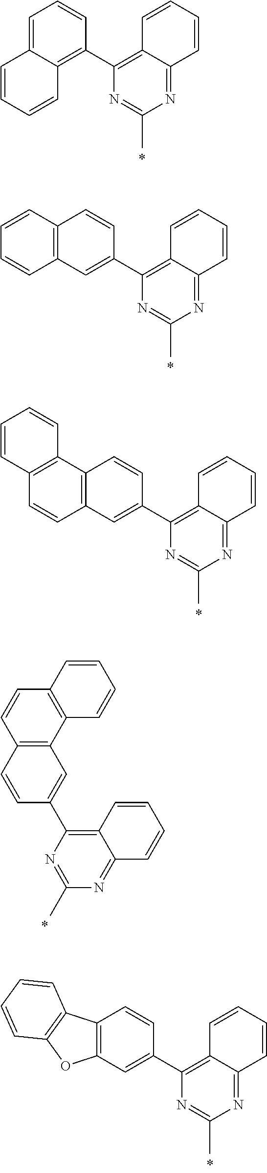


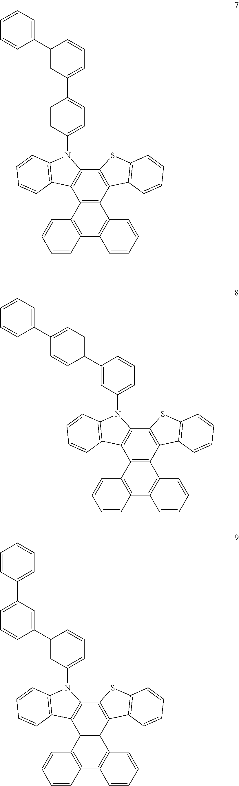


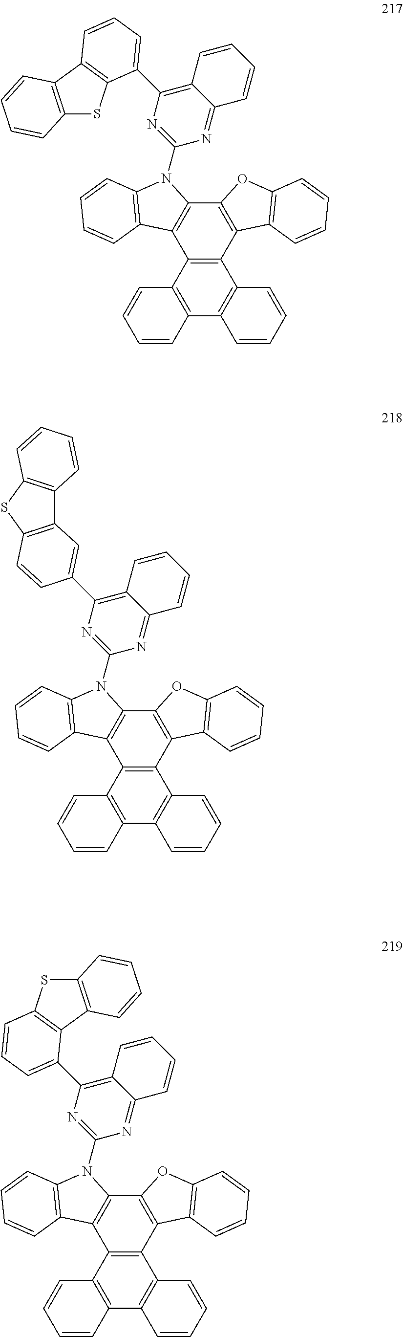


Applications Claiming Priority (2)
| Application Number | Priority Date | Filing Date | Title |
|---|---|---|---|
| KR10-2016-0120645 | 2016-09-21 | ||
| KR1020160120645A KR102018238B1 (en) | 2016-09-21 | 2016-09-21 | Compound for organic optoelectric device, composition for organic optoelectric device and organic optoelectric device and display device |
Publications (2)
| Publication Number | Publication Date |
|---|---|
| US20180083202A1 US20180083202A1 (en) | 2018-03-22 |
| US10096784B2 true US10096784B2 (en) | 2018-10-09 |
Family
ID=61621378
Family Applications (1)
| Application Number | Title | Priority Date | Filing Date |
|---|---|---|---|
| US15/677,491 Active US10096784B2 (en) | 2016-09-21 | 2017-08-15 | Compound for organic optoelectric device, composition for organic optoelectric device and organic optoelectric device and display device |
Country Status (3)
| Country | Link |
|---|---|
| US (1) | US10096784B2 (en) |
| KR (1) | KR102018238B1 (en) |
| CN (1) | CN107857772B (en) |
Families Citing this family (3)
| Publication number | Priority date | Publication date | Assignee | Title |
|---|---|---|---|---|
| CN112262135B (en) * | 2018-07-13 | 2023-10-24 | 株式会社Lg化学 | Heterocyclic compound and organic light-emitting device comprising same |
| CN110759850A (en) * | 2018-07-26 | 2020-02-07 | 北京鼎材科技有限公司 | Compound and application thereof |
| KR102193015B1 (en) | 2020-03-11 | 2020-12-18 | 주식회사 엘지화학 | Organic light emitting device |
Citations (7)
| Publication number | Priority date | Publication date | Assignee | Title |
|---|---|---|---|---|
| KR20120072784A (en) | 2010-12-24 | 2012-07-04 | 에스에프씨 주식회사 | Heterocyclic compounds and organic light-emitting diode including the same |
| KR101196093B1 (en) | 2010-05-06 | 2012-11-01 | 주식회사 두산 | Organic electroluminescence derivative and device using the phenanthrocarbazole |
| KR101219492B1 (en) | 2009-12-11 | 2013-01-28 | 삼성디스플레이 주식회사 | Compound Containing 5-Membered Heterocycle And Organic Electronic Element Using The Same, Terminal Thereof |
| KR20130050237A (en) | 2011-11-07 | 2013-05-15 | 덕산하이메탈(주) | Compound for organic electronic element, organic electronic element using the same, and a electronic device thereof |
| KR20130057397A (en) | 2011-11-23 | 2013-05-31 | 덕산하이메탈(주) | Compound for organic electronic element, organic electronic element using the same, and a electronic device thereof |
| KR101456521B1 (en) | 2008-07-14 | 2014-10-31 | 롬엔드하스전자재료코리아유한회사 | Novel organic electroluminescent compounds and organic electroluminescent device using the same |
| KR101470055B1 (en) | 2011-07-11 | 2014-12-08 | 주식회사 두산 | Organic electroluminescence device using the triphenylene derivative |
Family Cites Families (5)
| Publication number | Priority date | Publication date | Assignee | Title |
|---|---|---|---|---|
| KR101498278B1 (en) * | 2012-01-18 | 2015-03-06 | 덕산네오룩스 주식회사 | Compound for organic electronic element, organic electronic element using the same, and an electronic device thereof |
| WO2015178732A1 (en) * | 2014-05-23 | 2015-11-26 | Rohm And Haas Electronic Materials Korea Ltd. | Multi-component host material and an organic electroluminescence device comprising the same |
| KR102321377B1 (en) * | 2014-06-09 | 2021-11-04 | 삼성디스플레이 주식회사 | Organic light- emitting devices |
| JP6181116B2 (en) * | 2014-07-24 | 2017-08-16 | ドク サン ネオルクス カンパニー リミテッド | Organic electronic device and electronic device including the same |
| KR102291492B1 (en) * | 2015-01-16 | 2021-08-20 | 삼성디스플레이 주식회사 | Organic light-emitting device |
-
2016
- 2016-09-21 KR KR1020160120645A patent/KR102018238B1/en active IP Right Grant
-
2017
- 2017-08-15 US US15/677,491 patent/US10096784B2/en active Active
- 2017-09-01 CN CN201710778673.3A patent/CN107857772B/en active Active
Patent Citations (8)
| Publication number | Priority date | Publication date | Assignee | Title |
|---|---|---|---|---|
| KR101456521B1 (en) | 2008-07-14 | 2014-10-31 | 롬엔드하스전자재료코리아유한회사 | Novel organic electroluminescent compounds and organic electroluminescent device using the same |
| KR101219492B1 (en) | 2009-12-11 | 2013-01-28 | 삼성디스플레이 주식회사 | Compound Containing 5-Membered Heterocycle And Organic Electronic Element Using The Same, Terminal Thereof |
| KR101196093B1 (en) | 2010-05-06 | 2012-11-01 | 주식회사 두산 | Organic electroluminescence derivative and device using the phenanthrocarbazole |
| US9017829B2 (en) * | 2010-05-06 | 2015-04-28 | Doosan Corporation | Phenanthrocarbazole compound, and organic electroluminescent device using same |
| KR20120072784A (en) | 2010-12-24 | 2012-07-04 | 에스에프씨 주식회사 | Heterocyclic compounds and organic light-emitting diode including the same |
| KR101470055B1 (en) | 2011-07-11 | 2014-12-08 | 주식회사 두산 | Organic electroluminescence device using the triphenylene derivative |
| KR20130050237A (en) | 2011-11-07 | 2013-05-15 | 덕산하이메탈(주) | Compound for organic electronic element, organic electronic element using the same, and a electronic device thereof |
| KR20130057397A (en) | 2011-11-23 | 2013-05-31 | 덕산하이메탈(주) | Compound for organic electronic element, organic electronic element using the same, and a electronic device thereof |
Also Published As
| Publication number | Publication date |
|---|---|
| KR20180032021A (en) | 2018-03-29 |
| KR102018238B1 (en) | 2019-09-04 |
| CN107857772A (en) | 2018-03-30 |
| CN107857772B (en) | 2020-06-26 |
| US20180083202A1 (en) | 2018-03-22 |
Similar Documents
| Publication | Publication Date | Title |
|---|---|---|
| US20230209997A1 (en) | Organic alloy for organic optoelectronic device, organic optoelectronic device, and display device | |
| US10538510B2 (en) | Compound for organic optoelectronic device, composition for organic optoelectronic device and organic optoelectronic device and display device | |
| US10050212B2 (en) | Organic optoelectric device and display device | |
| US20190198780A1 (en) | Organic compound and composition and organic optoelectronic device and display device | |
| US10276804B2 (en) | Compound for organic optoelectronic element, organic optoelectronic element comprising same, and display device | |
| US20230255109A1 (en) | Compound, composition and organic optoelectronic device and display device | |
| US11450813B2 (en) | Organic optoelectronic diode and display device | |
| US10873033B2 (en) | Organic compound, composition, organic optoelectronic diode, and display device | |
| US20160163995A1 (en) | Organic optoelectric device and display device | |
| US11362281B2 (en) | Compound for organic optoelectronic diode, composition for organic optoelectronic diode, organic optoelectronic diode, and display apparatus | |
| US20170104163A1 (en) | Composition for organic optoelectric diode, organic optoelectric diode, and display device | |
| US20170084845A1 (en) | Organic optoelectronic device and display device | |
| US20190198775A1 (en) | Composition and organic optoelectronic device and display device | |
| US20170309829A1 (en) | Composition for organic optoelectronic element, organic optoelectronic element, and display device | |
| US20190280211A1 (en) | Organic optoelectronic device and display device | |
| US11926603B2 (en) | Compound, composition, organic optoelectronic diode, and display device | |
| US11158817B2 (en) | Compound for organic optoelectronic device, composition for organic optoelectronic device and organic optoelectronic device and display device | |
| US20210098704A1 (en) | Compound for organic optoelectronic device, composition for organic optoelectronic device, organic optoelectronic device and display device | |
| US11839152B2 (en) | Compound for organic photoelectronic element, organic photoelectronic element, and display device | |
| US10096784B2 (en) | Compound for organic optoelectric device, composition for organic optoelectric device and organic optoelectric device and display device | |
| US10032999B2 (en) | Compound for organic optoelectric device, composition for organic optoelectric device and organic optoelectric device and display device | |
| US10505125B2 (en) | Compound for organic optoelectronic diode, organic optoelectronic diode comprising same, and display device | |
| US10096777B2 (en) | Composition for organic optoelectric device and organic optoelectric device and display device | |
| US10505126B2 (en) | Composition for organic optoelectric device and organic optoelectric device and display device | |
| US20210104684A1 (en) | Compound for organic optoelectronic device, organic optoelectronic device and display device |
Legal Events
| Date | Code | Title | Description |
|---|---|---|---|
| AS | Assignment |
Owner name: SAMSUNG SDI CO., LTD., KOREA, REPUBLIC OF Free format text: ASSIGNMENT OF ASSIGNORS INTEREST;ASSIGNORS:KIM, BYUNGKU;KANG, DONG MIN;LUI, JINHYUN;AND OTHERS;REEL/FRAME:043297/0453 Effective date: 20170804 Owner name: SAMSUNG ELECTRONICS CO., LTD., KOREA, REPUBLIC OF Free format text: ASSIGNMENT OF ASSIGNORS INTEREST;ASSIGNORS:KIM, BYUNGKU;KANG, DONG MIN;LUI, JINHYUN;AND OTHERS;REEL/FRAME:043297/0453 Effective date: 20170804 |
|
| STCF | Information on status: patent grant |
Free format text: PATENTED CASE |
|
| AS | Assignment |
Owner name: SAMSUNG ELECTRONICS CO., LTD., KOREA, REPUBLIC OF Free format text: ASSIGNMENT OF ASSIGNORS INTEREST;ASSIGNORS:SAMSUNG SDI CO., LTD.;SAMSUNG ELECTRONICS CO., LTD.;REEL/FRAME:051338/0532 Effective date: 20191216 Owner name: SAMSUNG SDI CO., LTD., KOREA, REPUBLIC OF Free format text: ASSIGNMENT OF ASSIGNORS INTEREST;ASSIGNORS:SAMSUNG SDI CO., LTD.;SAMSUNG ELECTRONICS CO., LTD.;REEL/FRAME:051338/0532 Effective date: 20191216 |
|
| MAFP | Maintenance fee payment |
Free format text: PAYMENT OF MAINTENANCE FEE, 4TH YEAR, LARGE ENTITY (ORIGINAL EVENT CODE: M1551); ENTITY STATUS OF PATENT OWNER: LARGE ENTITY Year of fee payment: 4 |