US10078922B2 - Eye tracking for display resolution adjustment in a virtual reality system - Google Patents

Eye tracking for display resolution adjustment in a virtual reality system Download PDF

Info

Publication number
US10078922B2
US10078922B2 US15/068,380 US201615068380A US10078922B2 US 10078922 B2 US10078922 B2 US 10078922B2 US 201615068380 A US201615068380 A US 201615068380A US 10078922 B2 US10078922 B2 US 10078922B2
Authority
US
United States
Prior art keywords
resolution
region
virtual reality
data
rows
Prior art date
Legal status (The legal status is an assumption and is not a legal conclusion. Google has not performed a legal analysis and makes no representation as to the accuracy of the status listed.)
Active
Application number
US15/068,380
Other versions
US20160267716A1 (en
Inventor
Nirav Rajendra Patel
Current Assignee (The listed assignees may be inaccurate. Google has not performed a legal analysis and makes no representation or warranty as to the accuracy of the list.)
Meta Platforms Technologies LLC
Original Assignee
Oculus VR Inc
Priority date (The priority date is an assumption and is not a legal conclusion. Google has not performed a legal analysis and makes no representation as to the accuracy of the date listed.)
Filing date
Publication date
Application filed by Oculus VR Inc filed Critical Oculus VR Inc
Priority to US15/068,380 priority Critical patent/US10078922B2/en
Assigned to OCULUS VR, LLC reassignment OCULUS VR, LLC ASSIGNMENT OF ASSIGNORS INTEREST (SEE DOCUMENT FOR DETAILS). Assignors: PATEL, NIRAV RAJENDRA
Publication of US20160267716A1 publication Critical patent/US20160267716A1/en
Assigned to FACEBOOK TECHNOLOGIES, LLC reassignment FACEBOOK TECHNOLOGIES, LLC CHANGE OF NAME (SEE DOCUMENT FOR DETAILS). Assignors: OCULUS VR, LLC
Application granted granted Critical
Publication of US10078922B2 publication Critical patent/US10078922B2/en
Assigned to META PLATFORMS TECHNOLOGIES, LLC reassignment META PLATFORMS TECHNOLOGIES, LLC CHANGE OF NAME (SEE DOCUMENT FOR DETAILS). Assignors: FACEBOOK TECHNOLOGIES, LLC
Active legal-status Critical Current
Anticipated expiration legal-status Critical

Links

Images

Classifications

    • GPHYSICS
    • G06COMPUTING; CALCULATING OR COUNTING
    • G06TIMAGE DATA PROCESSING OR GENERATION, IN GENERAL
    • G06T19/00Manipulating 3D models or images for computer graphics
    • G06T19/20Editing of 3D images, e.g. changing shapes or colours, aligning objects or positioning parts
    • GPHYSICS
    • G06COMPUTING; CALCULATING OR COUNTING
    • G06FELECTRIC DIGITAL DATA PROCESSING
    • G06F3/00Input arrangements for transferring data to be processed into a form capable of being handled by the computer; Output arrangements for transferring data from processing unit to output unit, e.g. interface arrangements
    • G06F3/01Input arrangements or combined input and output arrangements for interaction between user and computer
    • G06F3/011Arrangements for interaction with the human body, e.g. for user immersion in virtual reality
    • G06F3/013Eye tracking input arrangements
    • GPHYSICS
    • G06COMPUTING; CALCULATING OR COUNTING
    • G06FELECTRIC DIGITAL DATA PROCESSING
    • G06F3/00Input arrangements for transferring data to be processed into a form capable of being handled by the computer; Output arrangements for transferring data from processing unit to output unit, e.g. interface arrangements
    • G06F3/01Input arrangements or combined input and output arrangements for interaction between user and computer
    • G06F3/048Interaction techniques based on graphical user interfaces [GUI]
    • G06F3/0484Interaction techniques based on graphical user interfaces [GUI] for the control of specific functions or operations, e.g. selecting or manipulating an object, an image or a displayed text element, setting a parameter value or selecting a range
    • GPHYSICS
    • G09EDUCATION; CRYPTOGRAPHY; DISPLAY; ADVERTISING; SEALS
    • G09GARRANGEMENTS OR CIRCUITS FOR CONTROL OF INDICATING DEVICES USING STATIC MEANS TO PRESENT VARIABLE INFORMATION
    • G09G3/00Control arrangements or circuits, of interest only in connection with visual indicators other than cathode-ray tubes
    • G09G3/20Control arrangements or circuits, of interest only in connection with visual indicators other than cathode-ray tubes for presentation of an assembly of a number of characters, e.g. a page, by composing the assembly by combination of individual elements arranged in a matrix no fixed position being assigned to or needed to be assigned to the individual characters or partial characters
    • G09G3/22Control arrangements or circuits, of interest only in connection with visual indicators other than cathode-ray tubes for presentation of an assembly of a number of characters, e.g. a page, by composing the assembly by combination of individual elements arranged in a matrix no fixed position being assigned to or needed to be assigned to the individual characters or partial characters using controlled light sources
    • G09G3/30Control arrangements or circuits, of interest only in connection with visual indicators other than cathode-ray tubes for presentation of an assembly of a number of characters, e.g. a page, by composing the assembly by combination of individual elements arranged in a matrix no fixed position being assigned to or needed to be assigned to the individual characters or partial characters using controlled light sources using electroluminescent panels
    • G09G3/32Control arrangements or circuits, of interest only in connection with visual indicators other than cathode-ray tubes for presentation of an assembly of a number of characters, e.g. a page, by composing the assembly by combination of individual elements arranged in a matrix no fixed position being assigned to or needed to be assigned to the individual characters or partial characters using controlled light sources using electroluminescent panels semiconductive, e.g. using light-emitting diodes [LED]
    • G09G3/3208Control arrangements or circuits, of interest only in connection with visual indicators other than cathode-ray tubes for presentation of an assembly of a number of characters, e.g. a page, by composing the assembly by combination of individual elements arranged in a matrix no fixed position being assigned to or needed to be assigned to the individual characters or partial characters using controlled light sources using electroluminescent panels semiconductive, e.g. using light-emitting diodes [LED] organic, e.g. using organic light-emitting diodes [OLED]
    • G09G3/3225Control arrangements or circuits, of interest only in connection with visual indicators other than cathode-ray tubes for presentation of an assembly of a number of characters, e.g. a page, by composing the assembly by combination of individual elements arranged in a matrix no fixed position being assigned to or needed to be assigned to the individual characters or partial characters using controlled light sources using electroluminescent panels semiconductive, e.g. using light-emitting diodes [LED] organic, e.g. using organic light-emitting diodes [OLED] using an active matrix
    • G09G3/3258Control arrangements or circuits, of interest only in connection with visual indicators other than cathode-ray tubes for presentation of an assembly of a number of characters, e.g. a page, by composing the assembly by combination of individual elements arranged in a matrix no fixed position being assigned to or needed to be assigned to the individual characters or partial characters using controlled light sources using electroluminescent panels semiconductive, e.g. using light-emitting diodes [LED] organic, e.g. using organic light-emitting diodes [OLED] using an active matrix with pixel circuitry controlling the voltage across the light-emitting element
    • GPHYSICS
    • G09EDUCATION; CRYPTOGRAPHY; DISPLAY; ADVERTISING; SEALS
    • G09GARRANGEMENTS OR CIRCUITS FOR CONTROL OF INDICATING DEVICES USING STATIC MEANS TO PRESENT VARIABLE INFORMATION
    • G09G5/00Control arrangements or circuits for visual indicators common to cathode-ray tube indicators and other visual indicators
    • G09G5/36Control arrangements or circuits for visual indicators common to cathode-ray tube indicators and other visual indicators characterised by the display of a graphic pattern, e.g. using an all-points-addressable [APA] memory
    • G09G5/37Details of the operation on graphic patterns
    • G09G5/373Details of the operation on graphic patterns for modifying the size of the graphic pattern
    • GPHYSICS
    • G09EDUCATION; CRYPTOGRAPHY; DISPLAY; ADVERTISING; SEALS
    • G09GARRANGEMENTS OR CIRCUITS FOR CONTROL OF INDICATING DEVICES USING STATIC MEANS TO PRESENT VARIABLE INFORMATION
    • G09G5/00Control arrangements or circuits for visual indicators common to cathode-ray tube indicators and other visual indicators
    • G09G5/36Control arrangements or circuits for visual indicators common to cathode-ray tube indicators and other visual indicators characterised by the display of a graphic pattern, e.g. using an all-points-addressable [APA] memory
    • G09G5/39Control of the bit-mapped memory
    • G09G5/395Arrangements specially adapted for transferring the contents of the bit-mapped memory to the screen
    • GPHYSICS
    • G06COMPUTING; CALCULATING OR COUNTING
    • G06TIMAGE DATA PROCESSING OR GENERATION, IN GENERAL
    • G06T2219/00Indexing scheme for manipulating 3D models or images for computer graphics
    • G06T2219/20Indexing scheme for editing of 3D models
    • G06T2219/2016Rotation, translation, scaling
    • GPHYSICS
    • G09EDUCATION; CRYPTOGRAPHY; DISPLAY; ADVERTISING; SEALS
    • G09GARRANGEMENTS OR CIRCUITS FOR CONTROL OF INDICATING DEVICES USING STATIC MEANS TO PRESENT VARIABLE INFORMATION
    • G09G2310/00Command of the display device
    • G09G2310/02Addressing, scanning or driving the display screen or processing steps related thereto
    • G09G2310/0224Details of interlacing
    • GPHYSICS
    • G09EDUCATION; CRYPTOGRAPHY; DISPLAY; ADVERTISING; SEALS
    • G09GARRANGEMENTS OR CIRCUITS FOR CONTROL OF INDICATING DEVICES USING STATIC MEANS TO PRESENT VARIABLE INFORMATION
    • G09G2310/00Command of the display device
    • G09G2310/02Addressing, scanning or driving the display screen or processing steps related thereto
    • G09G2310/0264Details of driving circuits
    • G09G2310/0291Details of output amplifiers or buffers arranged for use in a driving circuit
    • GPHYSICS
    • G09EDUCATION; CRYPTOGRAPHY; DISPLAY; ADVERTISING; SEALS
    • G09GARRANGEMENTS OR CIRCUITS FOR CONTROL OF INDICATING DEVICES USING STATIC MEANS TO PRESENT VARIABLE INFORMATION
    • G09G2310/00Command of the display device
    • G09G2310/04Partial updating of the display screen
    • GPHYSICS
    • G09EDUCATION; CRYPTOGRAPHY; DISPLAY; ADVERTISING; SEALS
    • G09GARRANGEMENTS OR CIRCUITS FOR CONTROL OF INDICATING DEVICES USING STATIC MEANS TO PRESENT VARIABLE INFORMATION
    • G09G2340/00Aspects of display data processing
    • G09G2340/04Changes in size, position or resolution of an image
    • G09G2340/0407Resolution change, inclusive of the use of different resolutions for different screen areas
    • GPHYSICS
    • G09EDUCATION; CRYPTOGRAPHY; DISPLAY; ADVERTISING; SEALS
    • G09GARRANGEMENTS OR CIRCUITS FOR CONTROL OF INDICATING DEVICES USING STATIC MEANS TO PRESENT VARIABLE INFORMATION
    • G09G2354/00Aspects of interface with display user

Definitions

  • the present disclosure generally relates to virtual reality systems and display operation in a virtual reality system.
  • Electronic displays include a plurality of pixels, which may each include a plurality of sub-pixels (e.g., a red sub-pixel, a green sub-pixel, etc.). Most displays are designed for use with cellphones, tablets and televisions. However, the characteristics of most displays are not ideal for use in a virtual reality (VR) headset where performance requirements (e.g. resolution and refresh rate) are more stringent than in typical displays.
  • VR virtual reality
  • a display device comprises a display screen.
  • the display screen includes a first pixel row of first pixels having respective storage capacitors, the first pixels connected to a first scan line, a second pixel row of second pixels having respective storage capacitors, the second pixels connected to a second scan line, first data lines connected to the first pixel row, and second data lines connected to the second pixel row.
  • a first data driver circuit drives the first pixel row via the first data lines.
  • a second data driver circuit drives the second pixel row via the second data lines.
  • a display device comprises a display screen having a plurality of pixels organized into pixel columns and pixel rows.
  • a resolution circuit stores resolution configuration data indicative of a location of a first region of the display screen operating in reduced resolution and indicative of a location of a second region of the display screen operating in full resolution.
  • a selective scaling circuit receives image data and processes the image data based on the resolution configuration data, the selective scaling circuit upscaling a first portion of the image data for the first region of the display screen and not upscaling a second portion of the image data for the second region of the display screen.
  • a virtual reality system comprises a virtual reality headset.
  • the headset comprises a display having a first region operating in reduced resolution and a second region operating in full resolution.
  • the headset also comprises an eye tracking sensor to generate gaze data indicative of a gaze direction of the eye.
  • the virtual reality system adjusts a location of the second region operating in full resolution based on the gaze direction of the eye.
  • FIG. 1 is a block diagram of a virtual reality system environment, according to an embodiment.
  • FIG. 2A is a wire diagram of a virtual reality headset, in accordance with an embodiment.
  • FIG. 2B is a cross section of the front rigid body of the embodiment of a VR headset shown in FIG. 2A .
  • FIG. 3 is an electronic display with dual row drivers, according to an embodiment.
  • FIG. 3A is the display from FIG. 3 where only the odd pixel rows are illustrated, according to an embodiment.
  • FIG. 3B is the display from FIG. 3 where only the even pixel rows are illustrated, according to an embodiment.
  • FIG. 4 is circuit diagram of a pixel P, according to an embodiment.
  • FIG. 5 is a timing diagram illustrating operation of the scan driver and data drivers, according to an embodiment.
  • FIG. 6A is a diagram illustrating a display screen, according to an embodiment.
  • FIG. 6B is a diagram illustrating a display screen with configurable effective resolution.
  • FIG. 7 illustrates a timing controller and data drivers supporting configurable effective resolution, according to an embodiment.
  • FIG. 8A illustrates selective scaling circuitry supporting configurable vertical resolution, according to one specific embodiment.
  • FIG. 8B illustrates selective scaling circuitry supporting configurable horizontal and vertical resolution, according to another embodiment.
  • FIG. 9A-9H illustrate operation of the display when operating in different resolution modes, according to an embodiment.
  • FIGS. 10A and 10B are diagrams illustrating the use of eye tracking to control a full resolution region of the display, according to an embodiment.
  • FIG. 11 is an interaction diagram for a virtual reality system that uses eye tracking to control a full resolution region of the display, according to an embodiment.
  • FIG. 12 illustrates the hardware architecture of computing device, according to one embodiment.
  • FIG. 1 is a block diagram of a virtual reality (VR) system environment 100 , according to an embodiment.
  • the system environment 100 shown by FIG. 1 comprises a VR headset 105 and a VR input interface 140 that are each coupled to the VR console 110 through wired connections 190 and 192 .
  • the wired connection 190 can be a video cable coupling the VR headset 105 to the VR console 110 .
  • the devices may communicate wirelessly instead of through wired connections.
  • FIG. 1 shows an example system 100 including one VR headset 105 and one VR input interface 140
  • any number of these components may be included in the system 100 .
  • different and/or additional components may be included in the system environment 100 .
  • the VR headset 105 is a head-mounted device that presents media to a user and is an example of a display device. Examples of media presented by the VR head set include one or more images, video, audio, or some combination thereof. In some embodiments, audio is presented via an external device (e.g., speakers and/or headphones) that receives audio information from the VR headset 105 , the VR console 110 , or both, and presents audio data based on the audio information.
  • An embodiment of the VR headset 105 is further described below in conjunction with FIGS. 2A and 2B .
  • the VR headset 105 may comprise one or more rigid bodies, which may be rigidly or non-rigidly coupled to each other together. A rigid coupling between rigid bodies causes the coupled rigid bodies to act as a single rigid entity. In contrast, a non-rigid coupling between rigid bodies allows the rigid bodies to move relative to each other.
  • the VR headset 105 includes an electronic display 115 , eye tracking sensor 118 , and communication interface 125 .
  • the VR headset 105 may include other components not shown in FIG. 100 , such as position sensors and location sensors (not shown).
  • the interface 125 sends data to and receives data from the virtual reality console via the wired connection 190 .
  • the electronic display 115 displays images to the user in accordance with image data received from the VR console 110 .
  • the electronic display 115 may comprise a single electronic display or multiple electronic displays (e.g., a display for each eye of a user).
  • Examples of the electronic display 115 include: an organic light emitting diode (OLED) display, a liquid crystal display (LCD), or other types of displays.
  • OLED organic light emitting diode
  • LCD liquid crystal display
  • the electronic display 115 includes a display screen having a matrix of pixels organized into pixel columns and pixel rows.
  • the electronic display 115 also includes display circuitry that receives image data from the virtual reality console 110 and generates pixel driving signals in order to produce visual images on the display screen from the image data.
  • the electronic display 115 includes twice the number of data lines and data drivers of a typical display.
  • the increased data lines and connection of the data lines to the pixels allows the refresh rate of the electronic display 115 to be doubled in frequency.
  • the higher refresh rates increase the realism of moving images shown on the electronic display 115 .
  • the refresh rate can be maintained while increasing the time allowed per row to charge the pixel capacitors.
  • the electronic display 115 can be selectively configured to have a higher effective resolution in a section of the screen that matches the direction of the user's gaze, while having a lower effective resolution in other sections of the screen not being viewed by a user. This reduces the required bandwidth needed to provide image data from the virtual reality console 110 to the virtual reality headset 105 via the wired connection 190 without any perceptible loss in image quality.
  • Eye tracking sensor 118 tracks the gaze of a user's eye and generates gaze data indicative of gaze direction of the user's eye.
  • an eye tracking sensor 118 is a camera that captures infrared light reflected off the pupil of the eye with an image sensor, and which generates gaze data in the form of captured images.
  • the gaze data is then transmitted to the virtual reality console 110 , where the images are processed by the eye tracking module 150 to extract gaze direction from changes in reflections.
  • the gaze direction is then used to selectively adjust the region of the display 115 that is to have higher resolution. The higher resolution region is continuously moved to track the user's gaze direction.
  • the eye tracking module 150 may be located within the virtual reality headset 105 such that the gaze direction is determined within the headset 105 itself.
  • Other examples of eye tracking sensors 118 are also possible, such as eye-attached tracking sensors and electric potential measurement sensors.
  • the VR input interface 140 is a device that allows a user to send action requests to the VR console 110 .
  • An action request is a request to perform a particular action.
  • An action request may be to start or end an application or to perform a particular action within the application.
  • the VR input interface 140 may include one or more input devices.
  • Example input devices include: a keyboard, a mouse, a game controller, or any other suitable device for receiving action requests and communicating the received action requests to the VR console 110 .
  • An action request received by the VR input interface 140 is communicated to the VR console 110 , which performs an action corresponding to the action request.
  • the VR input interface 140 may provide haptic feedback to the user in accordance with instructions received from the VR console 110 . For example, haptic feedback is provided when an action request is received, or the VR console 110 communicates instructions to the VR input interface 140 causing the VR input interface 140 to generate haptic feedback when the VR console 110 performs an action.
  • the VR console 110 provides media to the VR headset 105 for presentation to the user in accordance with information received from one or more of: the VR headset 105 , and the VR input interface 140 .
  • Examples of VR consoles 110 include computers, video game consoles, and other computing devices.
  • the VR console 110 includes an interface 142 , an application store 145 , an eye tracking module 150 , and a virtual reality (VR) engine module 155 .
  • the interface 142 sends data to and receives data (e.g. image data, gaze data) from the virtual reality headset 105 via the wired connection 190 .
  • the application store 145 stores one or more applications for execution by the VR console 110 .
  • An application is a group of instructions, that when executed by a processor, generates content for presentation to the user. Content generated by an application may be in response to inputs received from the user via movement of the HR headset 105 or the VR interface device 140 . Examples of applications include: gaming applications, conferencing applications, video playback application, or other suitable applications.
  • the VR engine module 155 executes applications within the system environment 100 and receives gaze direction information from the eye tracking module 150 . Based on the received information, the VR engine 155 determines how content images are to be processed and provided to the VR headset 105 .
  • the VR engine 155 determines, from the user's gaze direction, which region of the display 105 should be high resolution in order to match the user's gaze. For example, the VR engine 155 can estimate which pixels of the display 115 the gaze is focused on, and use those pixels as the center of the high resolution region (e.g. full resolution region). The VR engine 155 then generates resolution configuration data that specifies the location of the reduced resolution and full resolution regions of the display 115 . This resolution configuration data is provided to the VR headset 105 via interface 142 so that the display 115 can be configured to support reduced and full resolution regions. The VR engine 155 then generates and provides image data to the virtual reality headset 105 for display in the reduced and full resolution versions. The location of the full resolution window is adjusted to match the user's gaze such that the portion of the display 115 being viewed by the user always appears to be clear and sharp.
  • the VR engine module 155 performs an action within an application executing on the VR console 110 in response to an action request received from the VR input interface 140 and provides feedback to the user that the action was performed.
  • the provided feedback may be visual or audible feedback via the VR headset 105 or haptic feedback via the VR input interface 140 .
  • FIG. 2A is a wire diagram of a virtual reality (VR) headset 105 , in accordance with an embodiment.
  • the VR headset 105 includes a front rigid body 205 and a band 210 .
  • the front rigid body 205 includes one or more electronic display elements of the electronic display 115 (not shown) and the eye tracking sensors 118 (not shown).
  • the front rigid body 205 includes a front side 220 a , a top side 220 b , a bottom side 220 c , a right side 220 d , and a left side 220 e.
  • FIG. 2B is a cross section of the front rigid body 205 of the embodiment of a VR headset 105 shown in FIG. 2A .
  • the front rigid body 205 includes an electronic display 115 , and an eye tracking sensor 118 that generates gaze data indicative of the direction of the eye's 245 gaze.
  • the eye tracking sensor 118 is pointed at the pupil 250 such that movements of the pupil 118 can be captured.
  • Some components may not be shown in FIG. 2B , such as an optical block between the eye 245 and display 115 that bends the light from the display 115 .
  • FIG. 3 is an electronic display 115 with dual row drivers, according to an embodiment.
  • the electronic display 115 includes an active matrix display screen 310 and display circuitry 320 .
  • the display screen 310 includes an active matrix of pixels P organized in pixel rows (R 1 -R 4 ) and pixel columns. Although not shown in FIG. 3 , generally each pixel P includes multiple sub-pixels producing red, green, and blue light and there would be additional data lines DL connected to each of the sub-pixels.
  • the display screen 310 includes data lines DL and scan lines SL connected to the pixels P.
  • Data lines DL carry data voltages to the pixels P that represent target brightness levels of the pixels.
  • Scan lines SL carry scan pulses to the pixels P that scan the data voltages into the pixels P.
  • Scan lines SL may also be referred to as gate lines. Only 16 pixels P, 4 scan lines SL and 8 data lines DL are shown in FIG. 3 for ease of illustration. However, the display screen 310 typically has a larger number of pixels P (e.g. millions of pixels P), scan lines SL and data lines DL.
  • Pixel P can represent any of the pixels P from FIG. 3 .
  • the pixel P is an OLED pixel.
  • the pixel P includes a scan transistor T 1 , a storage capacitor C, a driving transistor Td and an OLED D 1 .
  • scan transistor T 1 When a scan pulse is applied from the scan line SL to the gate of scan transistor T 1 , scan transistor T 1 turns on and the data voltage on the data line DL is latched or scanned into the storage capacitor C.
  • the data voltage stored in capacitor C turns on the driving transistor T 2 , which drives current through the OLED D 1 in accordance with the level of the data voltage and causes the OLED D 1 to emit light.
  • the pixel P may have a different structure that uses additional transistors and electrical components other than those shown in FIG. 4 .
  • each data line DL is connected to only half the pixel rows (R 1 -R 4 ).
  • the data lines DL can be divided into two subsets: odd data lines (DL- 1 , DL 3 , etc) and even data lines (DL- 2 , DL- 4 , etc).
  • the two odd and even data lines alternate with each other.
  • Odd data lines (DL- 1 , DL- 3 , etc) are connected only to odd pixel rows (R 1 , R 3 ).
  • the odd data lines (DL- 1 -DL 3 , etc) are not connected to even pixel rows (R 2 , R 4 ), and are therefore electrically isolated from the even pixel rows (R 2 , R 4 ).
  • Even data lines (DL- 2 , DL- 4 , etc) are connected only to even pixels rows (R 2 , R 4 ) but not odd pixels rows (R 2 , R 4 ), and are therefore electrically isolated from the even pixel rows (R 2 , R 4 ).
  • each pixel column is driven by a pair of data lines DL, and the pixels P in the column are connected in alternating manner between the pair of data lines DL.
  • data line DL- 1 is connected to the pixels P in the odd rows (e.g. SL- 1 , SL- 3 ).
  • Data line DL- 2 is only connected to the pixels P in the even rows (e.g. SL- 2 , SL- 4 ).
  • the display screen 310 includes two data drivers and twice as many data lines DL as conventional displays because each data line DL is only connected to half the pixels P in a column, such as the odd pixel rows or the even pixel rows, but not both.
  • the refresh rate of the display can be doubled because each subsequent pixel row can be scanned before the previous pixel row has completed its scanning.
  • the scan time for each pixel row can be increased while maintaining the same refresh rate.
  • FIG. 3A is the display from FIG. 3 where only the odd pixel rows are illustrated, according to an embodiment.
  • the even pixel rows are hidden for ease of explanation.
  • Odd scan line SL- 1 is connected to all of the pixels in one odd pixel row R 1 .
  • Odd scan line SL- 3 is connected to all of the pixels in another odd pixel row R 3 .
  • the odd data lines (DL- 1 , DL- 3 , etc) are connected to all of the odd pixel rows (R 1 , R 3 ), but are not connected to any of the even pixel rows.
  • FIG. 3B is the display from FIG. 3 where only the even pixel rows are illustrated, according to an embodiment.
  • the odd pixel rows are hidden for ease of explanation.
  • Even scan line SL- 2 is connected to all of the pixels in one even pixel row R 2 .
  • Even scan line SL- 4 is connected to all of the pixels in another even pixel row R 4 .
  • the even data lines (DL- 2 , DL- 4 , etc) are connected to all of the even pixel rows (R 2 , R 4 ), but are not connected to any of the odd pixel rows.
  • the display circuitry 320 includes a timing controller 330 , an odd row data driver 350 , an even row data driver 352 and a scan driver 340 .
  • the timing controller 330 , odd row data driver 350 , even row data driver 352 , and scan driver 340 may all reside on a single integrated circuit (IC), or on separate ICs.
  • the scan driver 340 may be fabricated with thin film transistors and be separate from the other circuits.
  • odd row data driver 350 and even row data driver 352 are located on opposite sides of the display screen 310 . Odd row data driver 350 is located at the top of the display screen, and even row data driver 352 is located on the bottom side of the display screen 310 .
  • the timing controller 330 receives image data 370 and allocates rows of the image data 370 between the odd data driver 350 and even data driver 352 . Odd rows of image data 372 are delivered to the odd data driver 450 . Even rows of image data 374 are delivered to the even data driver 352 .
  • the odd row data driver 350 converts the image data 372 into data voltages that are driven onto the data lines DL connected to the odd pixel rows (R 1 , R 3 ).
  • the even row data driver 352 converts the image data 374 into data voltages that are driven onto the data lines DL connected to the even pixel rows (R 2 , R 4 ).
  • the timing controller 330 also provides gate timing control signals 376 to control the operation of the scan driver 340 .
  • the scan driver 340 generates scan pulses that are driven onto the scan lines SL. Each scan pulse scans in the data voltages to a pixel row. The pixels of a pixel row hold the data voltages in their respective storage capacitors.
  • the timing diagram includes signal waveforms for scan lines SL- 1 through SL- 4 , and also for data lines DL- 1 and DL 2 .
  • Data voltages d 1 and d 3 are driven onto data line DL- 1 at different times.
  • Scan pulse sc 1 scans data voltage d 1 into a pixel P in the first pixel row R 1 .
  • Scan pulse sc 3 scans data voltage d 3 into a pixel P of the third pixel row R 3 .
  • Data voltages d 2 and d 4 are driven onto data line DL- 2 at different times.
  • Scan pulse sc 2 scans data voltage d 2 into a pixel P in the second pixel row R 2 .
  • Scan pulse sc 4 scans a data voltage d 4 into a pixel P of the fourth pixel row R 4 .
  • Scan pulses sc 1 -sc 4 are driven sequentially onto the scan lines SL.
  • Each scan pulse overlaps with a previous scan pulse and next scan pulse in time.
  • scan pulse sc 2 overlaps with scan pulse sc 1 and scan pulse sc 3 .
  • the scanning of each even pixel row thus overlaps with the scanning of each odd pixel row.
  • Each pixel row can begin scanning before a previous pixel row has completed scanning. This scanning overlap allows the refresh rate of the display to be increased because the scanning of one row does not need to be completed before scanning of the next row begins. Similarly, the refresh rate can be maintained while increasing the time allowed per row to charge the pixel capacitors.
  • FIG. 6A is a diagram illustrating pixels of an electronic display 115 , according to an embodiment.
  • the display screen has a fixed native resolution of 1080 ⁇ 1080 (i.e. 1080 pixels wide, 1080 pixels tall).
  • a frame of image data provided to the virtual reality headset 105 should match the native resolution of the display screen.
  • transferring a video stream to the virtual reality headset 105 in a resolution that matches the native resolution of the display screen 310 can consume a large amount of bandwidth that exceeds the limits of the wired connection 190 .
  • the electronic display 115 uses full resolution image frame data for one portion of the display screen, and uses reduced resolution image frame data for another portion of the display screen, thereby reducing the data bandwidth requirements of the wired connection 190 .
  • FIG. 6B is a diagram illustrating a display screen of a display 115 with configurable effective resolution.
  • the display 115 can be operated in a manner that causes it to have different effective resolutions in different regions of the display 115 .
  • Effective resolution may also be referred to herein as a supported resolution.
  • the display 115 uses full resolution image data to display a full resolution image in one portion of the display, resulting in a full resolution region 610 .
  • the display uses partial resolution image data to display a partial resolution image in another portion of the display, resulting in a reduced resolution region 620 .
  • the full resolution region 610 is shown as a window within and surrounded by the reduced resolution region 620 .
  • Image data 370 B provided for the full resolution region 610 matches the native resolution of the full resolution region 610 and can be directly applied to the display screen 310 without upscaling.
  • the full resolution region 610 can have a native resolution of 400 ⁇ 400. It has an effective resolution of 400 ⁇ 400 because the image displayed in that region is generated from image frame data 370 B having 400 ⁇ 400 resolution.
  • Image frame data 370 A provided for the reduced resolution region 620 is lower than the native resolution of the reduced resolution region 620 .
  • the driver circuit 320 receives the reduced resolution image data 370 A and upscales the image data before applying the upscaled image data to the display screen.
  • the reduced resolution region 620 can have a native resolution of 1080 ⁇ 1080. It has an effective resolution of 540 ⁇ 540 because the image displayed in that region is generated from image frame data 370 A having 540 ⁇ 540 resolution.
  • the image frame data 370 A is upscaled by 2 ⁇ in both the horizontal and vertical directions before it is displayed in the reduced resolution region 620 .
  • the full resolution region 610 and reduced resolution region 620 may be different in size and shape.
  • the upper pixel rows of the display 115 may be the full resolution region while the lower pixel rows of the display 115 is the reduced resolution region.
  • the sizes of the regions can be configured in any manner from the entire panel down to a single color in a row. Beneficially, operating only a portion of the display 115 in full resolution reduces the required bandwidth for image data transferred from the virtual reality console 110 to the virtual reality headset 105 .
  • FIG. 7 illustrates a timing controller 330 and data drivers 350 and 352 supporting configurable resolution, according to an embodiment.
  • the timing controller 330 is shown with a resolution register 705 and scaling circuitry 710 .
  • the resolution register 705 can be a portion of a memory dedicated to storing configuration data, or can be a dedicated circuit for storing resolution configuration data.
  • the resolution register 705 stores resolution configuration data 706 describing regions of the display 115 that are to be operated in full resolution and regions of the display 115 that are to operate in reduced resolution.
  • the resolution configuration data 706 may include row/column coordinates of the boundaries of the full resolution region 610 and row/column coordinates of the boundaries of the reduced resolution region 620 .
  • the resolution configuration data 706 may be provided by the VR console 110 and then stored in the resolution register 705 .
  • the resolution configuration data 706 may also include information describing whether the resolution is being reduced in a vertical direction, horizontal direction, or both.
  • the resolution configuration data 706 may also include information describing an amount of upscaling (e.g. 2 ⁇ , 4 ⁇ , none) that should be applied in each region of the display.
  • the selective scaling circuitry 710 receives image data 370 provided by the VR console 110 , and also reads the resolution configuration data 706 from the resolution register 705 .
  • the image data 370 can include both reduced resolution image data 370 A and full resolution image data 370 B.
  • the scaling circuitry 710 uses the resolution configuration data 706 in determining which portions of the image data 370 are reduced resolution image data 370 A intended for the reduced resolution region and which are full resolution image data 370 B intended for the full resolution region.
  • the data does not need upscaling and is directly passed on to the odd row data driver or even row data driver 352 .
  • the scaling circuitry 720 upscales the image data 370 in the vertical direction, horizontal direction, or both.
  • the upscaling allows low resolution image data 370 A to properly fill all of the pixels in the reduced resolution region 620 .
  • upscaling involves duplicating image pixel data without using interpolation.
  • Duplicating image pixel data in the vertical direction can include providing the same row of image data 370 to both the odd row data driver 350 and even row data driver 352 , which results in the same image being displayed in two adjacent pixel rows.
  • Duplicating image pixel data in the horizontal direction can include duplicating image pixel data across columns such that the same image pixel data is provided to adjacent pixels in a row.
  • the upscaling can include interpolation between adjacent pixels.
  • FIG. 8A illustrates selective scaling circuitry 710 supporting configurable vertical resolution, according to one specific embodiment.
  • the selective scaling circuitry 710 includes a de-multiplexer 804 , row buffers 806 and 808 , routing circuit 810 and control circuit 812 .
  • This embodiment of the selective scaling circuitry 710 can duplicate rows of image data and provide the duplicated rows to both the odd row data driver 350 and even row data driver 352 , which allows for adjustment of vertical resolution.
  • the circuitry shown in FIG. 8 is just one example of circuitry for adjusting vertical resolution, and in other embodiments other types of circuitry are possible.
  • De-multiplexer 804 receives the image data 370 and directs rows of the image data 370 to row buffer 806 or row buffer 808 .
  • De-multiplexer 804 is controlled by multiplexer control signal 802 .
  • Multiplexer control signal 802 switches states under control of the image data row clock (i.e. with each image data row) such that rows of image data are stored in alternating manner between row buffer 806 and row buffer 808 .
  • Routing circuit 810 selectively directs rows of image data stored in row buffer 806 and 808 to odd row data driver 350 or even row data driver 352 .
  • Control circuit 812 generates one or more routing control signals 813 that control the routing of rows through the routing circuit 810 .
  • Control circuit 812 generally changes the configuration of the routing circuit 810 at a rate that matches the scan frequency of the display.
  • the register configuration data 706 sets at which row to switch from reduced resolution mode to full resolution mode and back.
  • the state of the routing control signals 813 is controlled depending on whether an incoming row of the image data 370 is supposed to be handled in reduced resolution or full resolution mode, as indicated by the resolution configuration data 706 read from the resolution register 705 . This is explained in greater detail by reference to FIG. 9A-9H .
  • FIG. 9A-9H illustrate operation of the display 115 supporting different resolutions for different display regions, according to an embodiment.
  • the reduced resolution region of the display occupies pixel rows 1 - 4 and that the full resolution region of the display occupies pixel rows 5 - 7 .
  • FIG. 9A-9E illustrate operation of the display when operating in reduced resolution mode for the first four pixel rows of the display, which is the reduced resolution region.
  • FIG. 9F-9H illustrate operation of the display when operating in full resolution mode for pixel rows five through seven, which is the full resolution region.
  • an image data row IDR 1 is received and stored into row buffer 806 .
  • an image data row IDR 2 is received and stored into row buffer 808 .
  • image data row IDR 1 is routed from row buffer 806 to odd row data driver 350 and scanned into the first pixel row of the display screen 310 .
  • image data row IDR 1 is now routed from row buffer 806 to even row data driver 352 and scanned into the second pixel row of the display screen 310 .
  • an image data row IDR 3 is received and stored into row buffer 806 .
  • image data row IDR 2 is routed from row buffer 808 to the odd row data driver 350 and scanned into the third pixel row of the display screen 310 .
  • image data row IDR 2 is still being stored into row buffer 806 , image data row IDR 2 is now routed from row buffer 808 to the even row data driver 352 and scanned into the fourth pixel row of the display screen 310 .
  • an image data row IDR 4 is received and stored into row buffer 808 .
  • image data row IDR 3 is routed from row buffer 806 to the odd row data driver 350 and scanned into the fifth pixel row of the display screen 310 .
  • an image data row IDR 5 is received and stored into row buffer 806 .
  • image data row IDR 4 is routed from row buffer 808 to the even row data driver 352 and scanned into the sixth pixel row of the display screen 310 .
  • an image data row IDR 6 is received and stored into row buffer 808 .
  • image data row IDR 5 is routed from row buffer 806 to the odd row data driver 350 and scanned into the seventh pixel row of the display screen 310 .
  • the incoming image row clock is half the speed of the scan clock scanning the rows into the display screen. In full resolution mode, the incoming row image row clock is the same as the scan clock scanning the rows into the display screen.
  • FIG. 8B illustrates selective scaling circuitry 710 supporting configurable horizontal and vertical resolution, according to another embodiment.
  • the selective scaling circuitry 710 of FIG. 8B is similar to the selective scaling circuitry 710 of FIG. 8A , but now includes a column upscaling circuit 820 , which allows for adjustment of effective horizontal resolution.
  • the column upscaling circuit 820 can selectively duplicate pixels of the image data 370 across pixel columns so that reduced resolution image data can be upscaled to the native resolution of the display screen.
  • Control circuit 812 generates one or more control signals 816 that control whether the column upscaler 820 should upscale the incoming data 370 .
  • the control circuit 812 When the register configuration data indicates that incoming data is intended for the reduced resolution region 620 of the screen, the control circuit 812 generates the control signal 816 in one state (e.g. logic high) to enable horizontal upscaling.
  • the control circuit 812 When the register configuration data indicates that incoming data is intended for the reduced resolution region 610 of the screen, the control circuit 812 generates the control signal 816 in another state (e.g. logic low) to disable horizontal upscaling.
  • the state of the control signals 816 is controlled depending on whether an incoming portion of the image data 370 is supposed to be handled in reduced resolution or full resolution mode, as indicated by the resolution configuration data read from the resolution register 705 .
  • the column upscaler 820 outputs image data 822 that may or may not be horizontally upscaled, depending on whether upscaling was needed. In any case, a row of the image data 822 now includes data for a number of pixels that matches a number of pixels in a pixel row of the display screen 310 .
  • De-multiplexer 804 receives the image data 370 and directs rows of the image data 370 to row buffer 806 or row buffer 808 .
  • different amounts of upscaling may be applied to different portions of the image data 370 .
  • a high amount of upscaling e.g. 4 ⁇
  • a low amount of upscaling e.g. 2 ⁇ , no upscaling
  • FIGS. 10A and 10B are diagrams illustrating the use of eye tracking to control a full resolution region 710 of the display 115 , according to an embodiment.
  • FIG. 10A includes an eye 245 having a gaze 1000 directed to a portion of the display 115 .
  • the display 115 is controlled such that the full resolution region 610 tracks the user's gaze 1000 .
  • the gaze direction 1000 has moved to the left.
  • the full resolution region 610 is moved to the left to match the user's new gaze 1000 .
  • the foveal region of the retina is the only part of the retina that permits 100% visual acuity.
  • a VR headset 105 where the display 115 is placed close to the user's eye 245 , only a small portion of the display 100 is viewed by foveal region anyways while the rest of the display 115 is viewed by other parts of the retina.
  • there is no loss in clarity if the portion of the display outside of the foveal region is not in full resolution.
  • FIG. 11 is an interaction diagram for using eye tracking to control a full resolution region of the display 115 , according to an embodiment.
  • the VR headset 105 tracks the eye and generates gaze data indicative of a gaze direction of the user's eye.
  • the VR headset 105 transmits 1105 the gaze data to the VR console 110 .
  • the VR console 110 receives the gaze data and analyzes the gaze data to determine 1115 the user's gaze direction.
  • the VR console 110 determines, from the gaze direction, the region of the display that is to be full resolution and the region that is to have reduced resolution.
  • the VR console 110 attempts to match the full resolution region with the gaze direction of the user in order to track the user's eye movements.
  • the VR console 110 transmits 1125 resolution configuration data describing the adjusted location of the full resolution region, the adjusted location of the reduced resolution region or both sets of locations to the VR headset.
  • the VR headset 105 receives the resolution configuration data and stores 1130 the resolution configuration data in a resolution register.
  • steps 1120 , 1125 , and 1130 result are steps involved in the adjustment of the location of the full resolution region 620 .
  • the VR console 110 then generates 1135 image data for display at the VR headset 105 .
  • part of the image data is for the reduced resolution region 620 of the display, and part of the image data is for the full resolution region 610 of the display.
  • the VR console 110 transmits 1140 the image data to the VR headset 105 .
  • the VR headset 105 processes 1145 the image data in accordance with the resolution configuration data.
  • the processing includes upscaling portions of the image data corresponding to the reduced resolution region 620 of the display, and not upscaling portions of the image data corresponding to the full resolution region 610 of the display.
  • the VR headset 105 displays 1150 an image that has a full resolution region 610 and a partial resolution region 620 by providing the image data to the data drivers 350 and 352 .
  • the process also repeats 1155 continuously at periodic intervals so that the full resolution region 610 is periodically adjusted to track the user's gaze.
  • FIG. 12 illustrates the hardware architecture of computing device 1200 , according to one embodiment.
  • the computing device 1200 may be used as VR console 110 .
  • the computing device includes components such as a processor 1202 , a memory 1203 , a storage module 1204 , an input module (e.g., keyboard, mouse, and the like) 1206 , a display module 1207 and a communication interface 1205 , exchanging data and control signals with one another through a bus 1201 .
  • the storage module 1204 is implemented as one or more non-transitory computer readable storage media (e.g., hard disk drive), and stores software instructions 1240 that are executed by the processor 1202 in conjunction with the memory 1203 to implement the operations of the eye tracking module 150 , virtual reality engine module 155 , or other operations described herein. Operating system software and other application software may also be stored in the storage module 1204 to run on the processor 1202 .

Landscapes

  • Engineering & Computer Science (AREA)
  • Theoretical Computer Science (AREA)
  • Physics & Mathematics (AREA)
  • General Physics & Mathematics (AREA)
  • General Engineering & Computer Science (AREA)
  • Computer Hardware Design (AREA)
  • Human Computer Interaction (AREA)
  • Computer Graphics (AREA)
  • Software Systems (AREA)
  • Architecture (AREA)
  • Control Of Indicators Other Than Cathode Ray Tubes (AREA)

Abstract

A virtual reality system and a display device that can be used, for example, as part of the virtual reality system. The display device can have more than one data driver, such as an even row data driver and an odd row data driver. The display device can have a configurable resolution such that one region of the display device operates at full resolution while another region of the display device operates at a reduced resolution. The virtual reality system can also track an eye gaze and adjust the full resolution region of the display device to track the eye gaze.

Description

CROSS REFERENCE TO RELATED APPLICATIONS
The present application claims priority from U.S. Provisional Patent Application No. 62/131,705, filed on Mar. 11, 2015, the contents of which are incorporated by reference herein in their entirety.
BACKGROUND
The present disclosure generally relates to virtual reality systems and display operation in a virtual reality system.
Electronic displays include a plurality of pixels, which may each include a plurality of sub-pixels (e.g., a red sub-pixel, a green sub-pixel, etc.). Most displays are designed for use with cellphones, tablets and televisions. However, the characteristics of most displays are not ideal for use in a virtual reality (VR) headset where performance requirements (e.g. resolution and refresh rate) are more stringent than in typical displays.
SUMMARY
In one embodiment, a display device comprises a display screen. The display screen includes a first pixel row of first pixels having respective storage capacitors, the first pixels connected to a first scan line, a second pixel row of second pixels having respective storage capacitors, the second pixels connected to a second scan line, first data lines connected to the first pixel row, and second data lines connected to the second pixel row. Additionally, a first data driver circuit drives the first pixel row via the first data lines. A second data driver circuit drives the second pixel row via the second data lines.
In one embodiment, a display device comprises a display screen having a plurality of pixels organized into pixel columns and pixel rows. A resolution circuit stores resolution configuration data indicative of a location of a first region of the display screen operating in reduced resolution and indicative of a location of a second region of the display screen operating in full resolution. A selective scaling circuit receives image data and processes the image data based on the resolution configuration data, the selective scaling circuit upscaling a first portion of the image data for the first region of the display screen and not upscaling a second portion of the image data for the second region of the display screen.
In one embodiment, a virtual reality system, comprises a virtual reality headset. The headset comprises a display having a first region operating in reduced resolution and a second region operating in full resolution. The headset also comprises an eye tracking sensor to generate gaze data indicative of a gaze direction of the eye. The virtual reality system adjusts a location of the second region operating in full resolution based on the gaze direction of the eye.
BRIEF DESCRIPTION OF THE DRAWINGS
FIG. 1 is a block diagram of a virtual reality system environment, according to an embodiment.
FIG. 2A is a wire diagram of a virtual reality headset, in accordance with an embodiment.
FIG. 2B is a cross section of the front rigid body of the embodiment of a VR headset shown in FIG. 2A.
FIG. 3 is an electronic display with dual row drivers, according to an embodiment.
FIG. 3A is the display from FIG. 3 where only the odd pixel rows are illustrated, according to an embodiment.
FIG. 3B is the display from FIG. 3 where only the even pixel rows are illustrated, according to an embodiment.
FIG. 4 is circuit diagram of a pixel P, according to an embodiment.
FIG. 5 is a timing diagram illustrating operation of the scan driver and data drivers, according to an embodiment.
FIG. 6A is a diagram illustrating a display screen, according to an embodiment.
FIG. 6B is a diagram illustrating a display screen with configurable effective resolution.
FIG. 7 illustrates a timing controller and data drivers supporting configurable effective resolution, according to an embodiment.
FIG. 8A illustrates selective scaling circuitry supporting configurable vertical resolution, according to one specific embodiment.
FIG. 8B illustrates selective scaling circuitry supporting configurable horizontal and vertical resolution, according to another embodiment.
FIG. 9A-9H illustrate operation of the display when operating in different resolution modes, according to an embodiment.
FIGS. 10A and 10B are diagrams illustrating the use of eye tracking to control a full resolution region of the display, according to an embodiment.
FIG. 11 is an interaction diagram for a virtual reality system that uses eye tracking to control a full resolution region of the display, according to an embodiment.
FIG. 12 illustrates the hardware architecture of computing device, according to one embodiment.
The figures depict embodiments of the present disclosure for purposes of illustration only. One skilled in the art will readily recognize from the following description that alternative embodiments of the structures and methods illustrated herein may be employed without departing from the principles, or benefits touted, of the disclosure described herein.
DETAILED DESCRIPTION
System Overview
FIG. 1 is a block diagram of a virtual reality (VR) system environment 100, according to an embodiment. The system environment 100 shown by FIG. 1 comprises a VR headset 105 and a VR input interface 140 that are each coupled to the VR console 110 through wired connections 190 and 192. For example, the wired connection 190 can be a video cable coupling the VR headset 105 to the VR console 110. In other embodiments the devices may communicate wirelessly instead of through wired connections.
While FIG. 1 shows an example system 100 including one VR headset 105 and one VR input interface 140, in other embodiments any number of these components may be included in the system 100. For example, there may be multiple VR headsets 105 each having an associated VR input interface 140, with each VR headset 105 and VR input interface 140 communicating with the VR console 110. In alternative configurations, different and/or additional components may be included in the system environment 100.
The VR headset 105 is a head-mounted device that presents media to a user and is an example of a display device. Examples of media presented by the VR head set include one or more images, video, audio, or some combination thereof. In some embodiments, audio is presented via an external device (e.g., speakers and/or headphones) that receives audio information from the VR headset 105, the VR console 110, or both, and presents audio data based on the audio information. An embodiment of the VR headset 105 is further described below in conjunction with FIGS. 2A and 2B. The VR headset 105 may comprise one or more rigid bodies, which may be rigidly or non-rigidly coupled to each other together. A rigid coupling between rigid bodies causes the coupled rigid bodies to act as a single rigid entity. In contrast, a non-rigid coupling between rigid bodies allows the rigid bodies to move relative to each other.
The VR headset 105 includes an electronic display 115, eye tracking sensor 118, and communication interface 125. The VR headset 105 may include other components not shown in FIG. 100, such as position sensors and location sensors (not shown). The interface 125 sends data to and receives data from the virtual reality console via the wired connection 190.
The electronic display 115 displays images to the user in accordance with image data received from the VR console 110. In various embodiments, the electronic display 115 may comprise a single electronic display or multiple electronic displays (e.g., a display for each eye of a user). Examples of the electronic display 115 include: an organic light emitting diode (OLED) display, a liquid crystal display (LCD), or other types of displays.
The electronic display 115 includes a display screen having a matrix of pixels organized into pixel columns and pixel rows. The electronic display 115 also includes display circuitry that receives image data from the virtual reality console 110 and generates pixel driving signals in order to produce visual images on the display screen from the image data.
In one embodiment, the electronic display 115 includes twice the number of data lines and data drivers of a typical display. The increased data lines and connection of the data lines to the pixels allows the refresh rate of the electronic display 115 to be doubled in frequency. The higher refresh rates increase the realism of moving images shown on the electronic display 115. Similarly, the refresh rate can be maintained while increasing the time allowed per row to charge the pixel capacitors.
In one embodiment, the electronic display 115 can be selectively configured to have a higher effective resolution in a section of the screen that matches the direction of the user's gaze, while having a lower effective resolution in other sections of the screen not being viewed by a user. This reduces the required bandwidth needed to provide image data from the virtual reality console 110 to the virtual reality headset 105 via the wired connection 190 without any perceptible loss in image quality.
Eye tracking sensor 118 tracks the gaze of a user's eye and generates gaze data indicative of gaze direction of the user's eye. One example of an eye tracking sensor 118 is a camera that captures infrared light reflected off the pupil of the eye with an image sensor, and which generates gaze data in the form of captured images. The gaze data is then transmitted to the virtual reality console 110, where the images are processed by the eye tracking module 150 to extract gaze direction from changes in reflections. The gaze direction is then used to selectively adjust the region of the display 115 that is to have higher resolution. The higher resolution region is continuously moved to track the user's gaze direction. In another embodiment, the eye tracking module 150 may be located within the virtual reality headset 105 such that the gaze direction is determined within the headset 105 itself. Other examples of eye tracking sensors 118 are also possible, such as eye-attached tracking sensors and electric potential measurement sensors.
The VR input interface 140 is a device that allows a user to send action requests to the VR console 110. An action request is a request to perform a particular action. For example, an action request may be to start or end an application or to perform a particular action within the application. The VR input interface 140 may include one or more input devices. Example input devices include: a keyboard, a mouse, a game controller, or any other suitable device for receiving action requests and communicating the received action requests to the VR console 110. An action request received by the VR input interface 140 is communicated to the VR console 110, which performs an action corresponding to the action request. In some embodiments, the VR input interface 140 may provide haptic feedback to the user in accordance with instructions received from the VR console 110. For example, haptic feedback is provided when an action request is received, or the VR console 110 communicates instructions to the VR input interface 140 causing the VR input interface 140 to generate haptic feedback when the VR console 110 performs an action.
The VR console 110 provides media to the VR headset 105 for presentation to the user in accordance with information received from one or more of: the VR headset 105, and the VR input interface 140. Examples of VR consoles 110 include computers, video game consoles, and other computing devices.
In the example shown in FIG. 1, the VR console 110 includes an interface 142, an application store 145, an eye tracking module 150, and a virtual reality (VR) engine module 155. The interface 142 sends data to and receives data (e.g. image data, gaze data) from the virtual reality headset 105 via the wired connection 190.
The application store 145 stores one or more applications for execution by the VR console 110. An application is a group of instructions, that when executed by a processor, generates content for presentation to the user. Content generated by an application may be in response to inputs received from the user via movement of the HR headset 105 or the VR interface device 140. Examples of applications include: gaming applications, conferencing applications, video playback application, or other suitable applications.
The VR engine module 155 executes applications within the system environment 100 and receives gaze direction information from the eye tracking module 150. Based on the received information, the VR engine 155 determines how content images are to be processed and provided to the VR headset 105.
In one embodiment, the VR engine 155 determines, from the user's gaze direction, which region of the display 105 should be high resolution in order to match the user's gaze. For example, the VR engine 155 can estimate which pixels of the display 115 the gaze is focused on, and use those pixels as the center of the high resolution region (e.g. full resolution region). The VR engine 155 then generates resolution configuration data that specifies the location of the reduced resolution and full resolution regions of the display 115. This resolution configuration data is provided to the VR headset 105 via interface 142 so that the display 115 can be configured to support reduced and full resolution regions. The VR engine 155 then generates and provides image data to the virtual reality headset 105 for display in the reduced and full resolution versions. The location of the full resolution window is adjusted to match the user's gaze such that the portion of the display 115 being viewed by the user always appears to be clear and sharp.
Additionally, the VR engine module 155 performs an action within an application executing on the VR console 110 in response to an action request received from the VR input interface 140 and provides feedback to the user that the action was performed. The provided feedback may be visual or audible feedback via the VR headset 105 or haptic feedback via the VR input interface 140.
FIG. 2A is a wire diagram of a virtual reality (VR) headset 105, in accordance with an embodiment. The VR headset 105 includes a front rigid body 205 and a band 210. The front rigid body 205 includes one or more electronic display elements of the electronic display 115 (not shown) and the eye tracking sensors 118 (not shown). The front rigid body 205 includes a front side 220 a, a top side 220 b, a bottom side 220 c, a right side 220 d, and a left side 220 e.
FIG. 2B is a cross section of the front rigid body 205 of the embodiment of a VR headset 105 shown in FIG. 2A. The front rigid body 205 includes an electronic display 115, and an eye tracking sensor 118 that generates gaze data indicative of the direction of the eye's 245 gaze. The eye tracking sensor 118 is pointed at the pupil 250 such that movements of the pupil 118 can be captured. Some components may not be shown in FIG. 2B, such as an optical block between the eye 245 and display 115 that bends the light from the display 115.
Dual Data Driver Display
FIG. 3 is an electronic display 115 with dual row drivers, according to an embodiment. The electronic display 115 includes an active matrix display screen 310 and display circuitry 320. The display screen 310 includes an active matrix of pixels P organized in pixel rows (R1-R4) and pixel columns. Although not shown in FIG. 3, generally each pixel P includes multiple sub-pixels producing red, green, and blue light and there would be additional data lines DL connected to each of the sub-pixels.
The display screen 310 includes data lines DL and scan lines SL connected to the pixels P. Data lines DL carry data voltages to the pixels P that represent target brightness levels of the pixels. Scan lines SL carry scan pulses to the pixels P that scan the data voltages into the pixels P. Scan lines SL may also be referred to as gate lines. Only 16 pixels P, 4 scan lines SL and 8 data lines DL are shown in FIG. 3 for ease of illustration. However, the display screen 310 typically has a larger number of pixels P (e.g. millions of pixels P), scan lines SL and data lines DL.
Referring briefly to FIG. 4, shown is a pixel P of the active matrix display screen 310, according to an embodiment. Pixel P can represent any of the pixels P from FIG. 3. The pixel P is an OLED pixel. The pixel P includes a scan transistor T1, a storage capacitor C, a driving transistor Td and an OLED D1. When a scan pulse is applied from the scan line SL to the gate of scan transistor T1, scan transistor T1 turns on and the data voltage on the data line DL is latched or scanned into the storage capacitor C. The data voltage stored in capacitor C turns on the driving transistor T2, which drives current through the OLED D1 in accordance with the level of the data voltage and causes the OLED D1 to emit light. In other embodiments the pixel P may have a different structure that uses additional transistors and electrical components other than those shown in FIG. 4.
Referring back to FIG. 3, each data line DL is connected to only half the pixel rows (R1-R4). The data lines DL can be divided into two subsets: odd data lines (DL-1, DL3, etc) and even data lines (DL-2, DL-4, etc). The two odd and even data lines alternate with each other. Odd data lines (DL-1, DL-3, etc) are connected only to odd pixel rows (R1, R3). The odd data lines (DL-1-DL3, etc) are not connected to even pixel rows (R2, R4), and are therefore electrically isolated from the even pixel rows (R2, R4). Even data lines (DL-2, DL-4, etc) are connected only to even pixels rows (R2, R4) but not odd pixels rows (R2, R4), and are therefore electrically isolated from the even pixel rows (R2, R4).
In other words, each pixel column is driven by a pair of data lines DL, and the pixels P in the column are connected in alternating manner between the pair of data lines DL. For example, data line DL-1 is connected to the pixels P in the odd rows (e.g. SL-1, SL-3). Data line DL-2 is only connected to the pixels P in the even rows (e.g. SL-2, SL-4).
The display screen 310 includes two data drivers and twice as many data lines DL as conventional displays because each data line DL is only connected to half the pixels P in a column, such as the odd pixel rows or the even pixel rows, but not both. By including twice as many data lines DL, the refresh rate of the display can be doubled because each subsequent pixel row can be scanned before the previous pixel row has completed its scanning. Alternatively, the scan time for each pixel row can be increased while maintaining the same refresh rate.
FIG. 3A is the display from FIG. 3 where only the odd pixel rows are illustrated, according to an embodiment. The even pixel rows are hidden for ease of explanation. Odd scan line SL-1 is connected to all of the pixels in one odd pixel row R1. Odd scan line SL-3 is connected to all of the pixels in another odd pixel row R3. The odd data lines (DL-1, DL-3, etc) are connected to all of the odd pixel rows (R1, R3), but are not connected to any of the even pixel rows.
FIG. 3B is the display from FIG. 3 where only the even pixel rows are illustrated, according to an embodiment. The odd pixel rows are hidden for ease of explanation. Even scan line SL-2 is connected to all of the pixels in one even pixel row R2. Even scan line SL-4 is connected to all of the pixels in another even pixel row R4. The even data lines (DL-2, DL-4, etc) are connected to all of the even pixel rows (R2, R4), but are not connected to any of the odd pixel rows.
Referring back to FIG. 3, the display circuitry 320 includes a timing controller 330, an odd row data driver 350, an even row data driver 352 and a scan driver 340. The timing controller 330, odd row data driver 350, even row data driver 352, and scan driver 340 may all reside on a single integrated circuit (IC), or on separate ICs. In some embodiments the scan driver 340 may be fabricated with thin film transistors and be separate from the other circuits. In one embodiment, odd row data driver 350 and even row data driver 352 are located on opposite sides of the display screen 310. Odd row data driver 350 is located at the top of the display screen, and even row data driver 352 is located on the bottom side of the display screen 310.
The timing controller 330 receives image data 370 and allocates rows of the image data 370 between the odd data driver 350 and even data driver 352. Odd rows of image data 372 are delivered to the odd data driver 450. Even rows of image data 374 are delivered to the even data driver 352. The odd row data driver 350 converts the image data 372 into data voltages that are driven onto the data lines DL connected to the odd pixel rows (R1, R3). The even row data driver 352 converts the image data 374 into data voltages that are driven onto the data lines DL connected to the even pixel rows (R2, R4).
The timing controller 330 also provides gate timing control signals 376 to control the operation of the scan driver 340. The scan driver 340 generates scan pulses that are driven onto the scan lines SL. Each scan pulse scans in the data voltages to a pixel row. The pixels of a pixel row hold the data voltages in their respective storage capacitors.
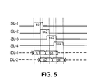
Referring now to FIG. 5, illustrated is a timing diagram illustrating operation of the scan driver 340 and data drivers 350 and 352, according to an embodiment. The timing diagram includes signal waveforms for scan lines SL-1 through SL-4, and also for data lines DL-1 and DL2.
Data voltages d1 and d3 are driven onto data line DL-1 at different times. Scan pulse sc1 scans data voltage d1 into a pixel P in the first pixel row R1. Scan pulse sc3 scans data voltage d3 into a pixel P of the third pixel row R3.
Data voltages d2 and d4 are driven onto data line DL-2 at different times. Scan pulse sc2 scans data voltage d2 into a pixel P in the second pixel row R2. Scan pulse sc4 scans a data voltage d4 into a pixel P of the fourth pixel row R4.
Scan pulses sc1-sc4 are driven sequentially onto the scan lines SL. Each scan pulse overlaps with a previous scan pulse and next scan pulse in time. For example, scan pulse sc2 overlaps with scan pulse sc1 and scan pulse sc3. The scanning of each even pixel row thus overlaps with the scanning of each odd pixel row. Each pixel row can begin scanning before a previous pixel row has completed scanning. This scanning overlap allows the refresh rate of the display to be increased because the scanning of one row does not need to be completed before scanning of the next row begins. Similarly, the refresh rate can be maintained while increasing the time allowed per row to charge the pixel capacitors.
Configurable Resolution in Dual Driver Display
FIG. 6A is a diagram illustrating pixels of an electronic display 115, according to an embodiment. The display screen has a fixed native resolution of 1080×1080 (i.e. 1080 pixels wide, 1080 pixels tall). To achieve the best image quality, a frame of image data provided to the virtual reality headset 105 should match the native resolution of the display screen. However, transferring a video stream to the virtual reality headset 105 in a resolution that matches the native resolution of the display screen 310 can consume a large amount of bandwidth that exceeds the limits of the wired connection 190. In one embodiment, the electronic display 115 uses full resolution image frame data for one portion of the display screen, and uses reduced resolution image frame data for another portion of the display screen, thereby reducing the data bandwidth requirements of the wired connection 190.
FIG. 6B is a diagram illustrating a display screen of a display 115 with configurable effective resolution. The display 115 can be operated in a manner that causes it to have different effective resolutions in different regions of the display 115. Effective resolution may also be referred to herein as a supported resolution. The display 115 uses full resolution image data to display a full resolution image in one portion of the display, resulting in a full resolution region 610. The display uses partial resolution image data to display a partial resolution image in another portion of the display, resulting in a reduced resolution region 620.
The full resolution region 610 is shown as a window within and surrounded by the reduced resolution region 620. Image data 370B provided for the full resolution region 610 matches the native resolution of the full resolution region 610 and can be directly applied to the display screen 310 without upscaling. For example, the full resolution region 610 can have a native resolution of 400×400. It has an effective resolution of 400×400 because the image displayed in that region is generated from image frame data 370B having 400×400 resolution.
Image frame data 370A provided for the reduced resolution region 620 is lower than the native resolution of the reduced resolution region 620. The driver circuit 320 receives the reduced resolution image data 370A and upscales the image data before applying the upscaled image data to the display screen. For example, the reduced resolution region 620 can have a native resolution of 1080×1080. It has an effective resolution of 540×540 because the image displayed in that region is generated from image frame data 370A having 540×540 resolution. The image frame data 370A is upscaled by 2× in both the horizontal and vertical directions before it is displayed in the reduced resolution region 620.
In other embodiments the full resolution region 610 and reduced resolution region 620 may be different in size and shape. For example, the upper pixel rows of the display 115 may be the full resolution region while the lower pixel rows of the display 115 is the reduced resolution region. The sizes of the regions can be configured in any manner from the entire panel down to a single color in a row. Beneficially, operating only a portion of the display 115 in full resolution reduces the required bandwidth for image data transferred from the virtual reality console 110 to the virtual reality headset 105.
FIG. 7 illustrates a timing controller 330 and data drivers 350 and 352 supporting configurable resolution, according to an embodiment. The timing controller 330 is shown with a resolution register 705 and scaling circuitry 710. In one embodiment, the resolution register 705 can be a portion of a memory dedicated to storing configuration data, or can be a dedicated circuit for storing resolution configuration data.
The resolution register 705 stores resolution configuration data 706 describing regions of the display 115 that are to be operated in full resolution and regions of the display 115 that are to operate in reduced resolution. For example, the resolution configuration data 706 may include row/column coordinates of the boundaries of the full resolution region 610 and row/column coordinates of the boundaries of the reduced resolution region 620. The resolution configuration data 706 may be provided by the VR console 110 and then stored in the resolution register 705. The resolution configuration data 706 may also include information describing whether the resolution is being reduced in a vertical direction, horizontal direction, or both. The resolution configuration data 706 may also include information describing an amount of upscaling (e.g. 2×, 4×, none) that should be applied in each region of the display.
The selective scaling circuitry 710 receives image data 370 provided by the VR console 110, and also reads the resolution configuration data 706 from the resolution register 705. For a single image frame, the image data 370 can include both reduced resolution image data 370A and full resolution image data 370B. The scaling circuitry 710 uses the resolution configuration data 706 in determining which portions of the image data 370 are reduced resolution image data 370A intended for the reduced resolution region and which are full resolution image data 370B intended for the full resolution region. For portions of the image data 370 intended for the full resolution region 610 (i.e. full resolution image data 370A), the data does not need upscaling and is directly passed on to the odd row data driver or even row data driver 352. For portions of the image data 370 intended for the low resolution region (i.e. reduced resolution image data 370A), the scaling circuitry 720 upscales the image data 370 in the vertical direction, horizontal direction, or both.
The upscaling allows low resolution image data 370A to properly fill all of the pixels in the reduced resolution region 620. Typically upscaling involves duplicating image pixel data without using interpolation. Duplicating image pixel data in the vertical direction can include providing the same row of image data 370 to both the odd row data driver 350 and even row data driver 352, which results in the same image being displayed in two adjacent pixel rows. Duplicating image pixel data in the horizontal direction can include duplicating image pixel data across columns such that the same image pixel data is provided to adjacent pixels in a row. In other embodiments, the upscaling can include interpolation between adjacent pixels.
FIG. 8A illustrates selective scaling circuitry 710 supporting configurable vertical resolution, according to one specific embodiment. The selective scaling circuitry 710 includes a de-multiplexer 804, row buffers 806 and 808, routing circuit 810 and control circuit 812. This embodiment of the selective scaling circuitry 710 can duplicate rows of image data and provide the duplicated rows to both the odd row data driver 350 and even row data driver 352, which allows for adjustment of vertical resolution. The circuitry shown in FIG. 8 is just one example of circuitry for adjusting vertical resolution, and in other embodiments other types of circuitry are possible.
De-multiplexer 804 receives the image data 370 and directs rows of the image data 370 to row buffer 806 or row buffer 808. De-multiplexer 804 is controlled by multiplexer control signal 802. Multiplexer control signal 802 switches states under control of the image data row clock (i.e. with each image data row) such that rows of image data are stored in alternating manner between row buffer 806 and row buffer 808. Routing circuit 810 selectively directs rows of image data stored in row buffer 806 and 808 to odd row data driver 350 or even row data driver 352.
Control circuit 812 generates one or more routing control signals 813 that control the routing of rows through the routing circuit 810. Control circuit 812 generally changes the configuration of the routing circuit 810 at a rate that matches the scan frequency of the display. The register configuration data 706 sets at which row to switch from reduced resolution mode to full resolution mode and back. Thus, the state of the routing control signals 813 is controlled depending on whether an incoming row of the image data 370 is supposed to be handled in reduced resolution or full resolution mode, as indicated by the resolution configuration data 706 read from the resolution register 705. This is explained in greater detail by reference to FIG. 9A-9H.
FIG. 9A-9H illustrate operation of the display 115 supporting different resolutions for different display regions, according to an embodiment. In FIG. 9A-9H, the reduced resolution region of the display occupies pixel rows 1-4 and that the full resolution region of the display occupies pixel rows 5-7. FIG. 9A-9E illustrate operation of the display when operating in reduced resolution mode for the first four pixel rows of the display, which is the reduced resolution region. FIG. 9F-9H illustrate operation of the display when operating in full resolution mode for pixel rows five through seven, which is the full resolution region.
Initially the display is in reduced region mode of operation for pixel rows one through four where pixel duplication is needed. In FIG. 9A, an image data row IDR1 is received and stored into row buffer 806.
In FIG. 9B, an image data row IDR2 is received and stored into row buffer 808. At the same time, image data row IDR1 is routed from row buffer 806 to odd row data driver 350 and scanned into the first pixel row of the display screen 310.
In FIG. 9C, while image data row IDR2 is still being stored into row buffer 808, image data row IDR1 is now routed from row buffer 806 to even row data driver 352 and scanned into the second pixel row of the display screen 310.
In FIG. 9D, an image data row IDR3 is received and stored into row buffer 806. At the same time, image data row IDR2 is routed from row buffer 808 to the odd row data driver 350 and scanned into the third pixel row of the display screen 310.
In FIG. 9E, while image data row IDR2 is still being stored into row buffer 806, image data row IDR2 is now routed from row buffer 808 to the even row data driver 352 and scanned into the fourth pixel row of the display screen 310.
The display now switches to full resolution mode of operation for pixel rows five through seven where pixel duplication is not needed. In FIG. 9F, an image data row IDR4 is received and stored into row buffer 808. At the same time, image data row IDR3 is routed from row buffer 806 to the odd row data driver 350 and scanned into the fifth pixel row of the display screen 310.
In FIG. 9G, an image data row IDR5 is received and stored into row buffer 806. At the same time, image data row IDR4 is routed from row buffer 808 to the even row data driver 352 and scanned into the sixth pixel row of the display screen 310.
In FIG. 9H, an image data row IDR6 is received and stored into row buffer 808. At the same time, image data row IDR5 is routed from row buffer 806 to the odd row data driver 350 and scanned into the seventh pixel row of the display screen 310.
It should be noted that, in reduced resolution mode, the incoming image row clock is half the speed of the scan clock scanning the rows into the display screen. In full resolution mode, the incoming row image row clock is the same as the scan clock scanning the rows into the display screen.
FIG. 8B illustrates selective scaling circuitry 710 supporting configurable horizontal and vertical resolution, according to another embodiment. The selective scaling circuitry 710 of FIG. 8B is similar to the selective scaling circuitry 710 of FIG. 8A, but now includes a column upscaling circuit 820, which allows for adjustment of effective horizontal resolution. The column upscaling circuit 820 can selectively duplicate pixels of the image data 370 across pixel columns so that reduced resolution image data can be upscaled to the native resolution of the display screen.
Control circuit 812 generates one or more control signals 816 that control whether the column upscaler 820 should upscale the incoming data 370. When the register configuration data indicates that incoming data is intended for the reduced resolution region 620 of the screen, the control circuit 812 generates the control signal 816 in one state (e.g. logic high) to enable horizontal upscaling. When the register configuration data indicates that incoming data is intended for the reduced resolution region 610 of the screen, the control circuit 812 generates the control signal 816 in another state (e.g. logic low) to disable horizontal upscaling. Thus, the state of the control signals 816 is controlled depending on whether an incoming portion of the image data 370 is supposed to be handled in reduced resolution or full resolution mode, as indicated by the resolution configuration data read from the resolution register 705.
The column upscaler 820 outputs image data 822 that may or may not be horizontally upscaled, depending on whether upscaling was needed. In any case, a row of the image data 822 now includes data for a number of pixels that matches a number of pixels in a pixel row of the display screen 310. De-multiplexer 804 receives the image data 370 and directs rows of the image data 370 to row buffer 806 or row buffer 808.
In another embodiment, different amounts of upscaling may be applied to different portions of the image data 370. For example, a high amount of upscaling (e.g. 4×) may be applied to image data intended for one display region, while a low amount of upscaling (e.g. 2×, no upscaling) may be applied to image data intended for another display region.
Eye Tracking Control of Display Resolution
FIGS. 10A and 10B are diagrams illustrating the use of eye tracking to control a full resolution region 710 of the display 115, according to an embodiment. FIG. 10A includes an eye 245 having a gaze 1000 directed to a portion of the display 115. The display 115 is controlled such that the full resolution region 610 tracks the user's gaze 1000. For example, in FIG. 10B, the gaze direction 1000 has moved to the left. As a result, the full resolution region 610 is moved to the left to match the user's new gaze 1000.
In a human eye, the foveal region of the retina is the only part of the retina that permits 100% visual acuity. In a VR headset 105 where the display 115 is placed close to the user's eye 245, only a small portion of the display 100 is viewed by foveal region anyways while the rest of the display 115 is viewed by other parts of the retina. Thus, to the human eye, there is no loss in clarity if the portion of the display outside of the foveal region is not in full resolution.
FIG. 11 is an interaction diagram for using eye tracking to control a full resolution region of the display 115, according to an embodiment. The VR headset 105 tracks the eye and generates gaze data indicative of a gaze direction of the user's eye. The VR headset 105 transmits 1105 the gaze data to the VR console 110. The VR console 110 receives the gaze data and analyzes the gaze data to determine 1115 the user's gaze direction.
The VR console 110 determines, from the gaze direction, the region of the display that is to be full resolution and the region that is to have reduced resolution. The VR console 110 attempts to match the full resolution region with the gaze direction of the user in order to track the user's eye movements. The VR console 110 transmits 1125 resolution configuration data describing the adjusted location of the full resolution region, the adjusted location of the reduced resolution region or both sets of locations to the VR headset. The VR headset 105 receives the resolution configuration data and stores 1130 the resolution configuration data in a resolution register. In one embodiment, steps 1120, 1125, and 1130 result are steps involved in the adjustment of the location of the full resolution region 620.
The VR console 110 then generates 1135 image data for display at the VR headset 105. In each image frame, part of the image data is for the reduced resolution region 620 of the display, and part of the image data is for the full resolution region 610 of the display. The VR console 110 transmits 1140 the image data to the VR headset 105. The VR headset 105 processes 1145 the image data in accordance with the resolution configuration data. The processing includes upscaling portions of the image data corresponding to the reduced resolution region 620 of the display, and not upscaling portions of the image data corresponding to the full resolution region 610 of the display. The VR headset 105 then displays 1150 an image that has a full resolution region 610 and a partial resolution region 620 by providing the image data to the data drivers 350 and 352.
The process also repeats 1155 continuously at periodic intervals so that the full resolution region 610 is periodically adjusted to track the user's gaze.
Other Considerations
FIG. 12 illustrates the hardware architecture of computing device 1200, according to one embodiment. In some embodiments, the computing device 1200 may be used as VR console 110. The computing device includes components such as a processor 1202, a memory 1203, a storage module 1204, an input module (e.g., keyboard, mouse, and the like) 1206, a display module 1207 and a communication interface 1205, exchanging data and control signals with one another through a bus 1201. The storage module 1204 is implemented as one or more non-transitory computer readable storage media (e.g., hard disk drive), and stores software instructions 1240 that are executed by the processor 1202 in conjunction with the memory 1203 to implement the operations of the eye tracking module 150, virtual reality engine module 155, or other operations described herein. Operating system software and other application software may also be stored in the storage module 1204 to run on the processor 1202.
The foregoing description of the embodiments of the disclosure has been presented for the purpose of illustration; it is not intended to be exhaustive or to limit the disclosure to the precise forms disclosed. Persons skilled in the relevant art can appreciate that many modifications and variations are possible in light of the above disclosure.
The language used in the specification has been principally selected for readability and instructional purposes, and it may not have been selected to delineate or circumscribe the inventive subject matter. It is therefore intended that the scope of the disclosure be limited not by this detailed description, but rather by any claims that issue on an application based hereon. Accordingly, the disclosed embodiments are intended to be illustrative, but not limiting, of the scope of the disclosure, which is set forth in the following claims.

Claims (12)

What is claimed is:
1. A virtual reality system, comprising:
a virtual reality headset comprising:
a display screen comprising a plurality of rows, and having a first region having a first native resolution and operating in reduced resolution by having an effective resolution lower than the first native resolution, and a second region having a second native resolution and operating in full resolution by having an effective resolution that is same as the second native resolution;
a selective scaling circuit configured to receive incoming rows of image data to be displayed on the display screen, and to scan the received rows of image data into rows of the display screen, wherein:
for the first region of the display screen, the rate at which incoming rows of image data are received is less than the rate at which the received rows are scanned into rows of the display screen, and
for the second region of the display screen, the rate at which the incoming rows of image data are received is the same as the rate at which the received rows are scanned into rows of the display screen; and
an eye tracking sensor to generate gaze data indicative of a gaze direction of the eye,
wherein a location of the second region operating in full resolution is adjusted based on the gaze direction of the eye.
2. The virtual reality system of claim 1, wherein the eye tracking sensor is a camera that generates gaze data in the form of an image of the eye.
3. The virtual reality system of claim 1, the location of the second region operating in full resolution is adjusted to match the gaze direction of the eye.
4. The virtual reality system of claim 1, further comprising:
a virtual reality console to receive the gaze data from the virtual reality headset, and to adjust the location of the second region operating in full resolution by transmitting resolution configuration data to the virtual reality headset indicative of an adjusted location of the second region of the display screen operating in full resolution.
5. The virtual reality system of claim 1, wherein the virtual reality console transmits image data to the virtual reality headset, and the virtual reality headset displays the image data on the display screen based on the resolution configuration data.
6. The virtual reality system of claim 1, wherein the second region is surrounded by the first region.
7. A method of operation in a virtual reality system, comprising:
displaying an image in a display of the virtual reality system, the display comprising a plurality of rows and including a first region having a first native resolution and operating in reduced resolution by having an effective resolution lower than the first native resolution, and a second region having a second native resolution and operating in full resolution by having an effective resolution that is same as the second native resolution, and wherein displaying the image comprises:
receiving incoming rows of the image to be displayed, and scanning the received image rows into rows of the display, wherein:
for the first region of the display, the rate at which incoming rows of the image are received is less than the rate at which the received rows are scanned into rows of the display, and
for the second region of the display, the rate at which the incoming rows of the image are received is the same as the rate at which the received rows are scanned into rows of the display;
generating gaze data indicative of a gaze direction of an eye; and
adjusting a location of the second region operating in full resolution based on the gaze direction of the eye.
8. The method of claim 7, wherein the gaze data is an image of the eye generated from a camera.
9. The method of claim 7, wherein the location of the second region operating in full resolution is adjusted to match the gaze direction of the eye.
10. The method of claim 7, further comprising:
receiving, at a virtual reality console, the gaze data from a virtual reality headset, and
wherein the location of the second region operating in full resolution is adjusted by transmitting resolution configuration data from the virtual reality console to the virtual reality headset indicative of an adjusted location of the second region of the display screen operating in full resolution.
11. The method of claim 7, wherein the virtual reality console transmits image data to the virtual reality headset, and the virtual reality headset displays the image data on the display screen based on the resolution configuration data.
12. The method of claim 7, wherein the second region is surrounded by the first region.
US15/068,380 2015-03-11 2016-03-11 Eye tracking for display resolution adjustment in a virtual reality system Active US10078922B2 (en)

Priority Applications (1)

Application Number Priority Date Filing Date Title
US15/068,380 US10078922B2 (en) 2015-03-11 2016-03-11 Eye tracking for display resolution adjustment in a virtual reality system

Applications Claiming Priority (2)

Application Number Priority Date Filing Date Title
US201562131705P 2015-03-11 2015-03-11
US15/068,380 US10078922B2 (en) 2015-03-11 2016-03-11 Eye tracking for display resolution adjustment in a virtual reality system

Publications (2)

Publication Number Publication Date
US20160267716A1 US20160267716A1 (en) 2016-09-15
US10078922B2 true US10078922B2 (en) 2018-09-18

Family

ID=56888097

Family Applications (3)

Application Number Title Priority Date Filing Date
US15/067,566 Active 2036-07-08 US10290156B2 (en) 2015-03-11 2016-03-11 Display device with dual data drivers
US15/068,326 Active 2036-08-19 US10417832B2 (en) 2015-03-11 2016-03-11 Display device supporting configurable resolution regions
US15/068,380 Active US10078922B2 (en) 2015-03-11 2016-03-11 Eye tracking for display resolution adjustment in a virtual reality system

Family Applications Before (2)

Application Number Title Priority Date Filing Date
US15/067,566 Active 2036-07-08 US10290156B2 (en) 2015-03-11 2016-03-11 Display device with dual data drivers
US15/068,326 Active 2036-08-19 US10417832B2 (en) 2015-03-11 2016-03-11 Display device supporting configurable resolution regions

Country Status (1)

Country Link
US (3) US10290156B2 (en)

Cited By (1)

* Cited by examiner, † Cited by third party
Publication number Priority date Publication date Assignee Title
US10636340B2 (en) * 2018-04-16 2020-04-28 Facebook Technologies, Llc Display with gaze-adaptive resolution enhancement

Families Citing this family (85)

* Cited by examiner, † Cited by third party
Publication number Priority date Publication date Assignee Title
US10269839B2 (en) * 2015-03-26 2019-04-23 Carestream Health, Inc. Apparatus and method using a dual gate TFT structure
US9704217B2 (en) 2015-04-20 2017-07-11 Intel Corporation Apparatus and method for non-uniform frame buffer rasterization
GB2548853B (en) * 2016-03-30 2020-09-23 Advanced Risc Mach Ltd Data processing
US20190335164A1 (en) * 2016-06-21 2019-10-31 Philips Lighting Holding B.V. Display system and method
JP6805603B2 (en) * 2016-07-26 2020-12-23 セイコーエプソン株式会社 Electro-optics, control methods for electro-optics and electronic devices
CN115064110A (en) * 2016-08-15 2022-09-16 苹果公司 Display with variable resolution
US11210990B2 (en) * 2016-08-16 2021-12-28 Apple Inc. Foveated display
US10482822B2 (en) 2016-09-09 2019-11-19 Apple Inc. Displays with multiple scanning modes
US10109240B2 (en) 2016-09-09 2018-10-23 Apple Inc. Displays with multiple scanning modes
KR102593456B1 (en) * 2016-09-30 2023-10-24 엘지디스플레이 주식회사 Virtual reality display device and method for driving the same
US10928638B2 (en) 2016-10-31 2021-02-23 Dolby Laboratories Licensing Corporation Eyewear devices with focus tunable lenses
KR20180057101A (en) * 2016-11-21 2018-05-30 엘지디스플레이 주식회사 Gate driving circuit and display panel using the same
CN107066079A (en) 2016-11-29 2017-08-18 阿里巴巴集团控股有限公司 Service implementation method and device based on virtual reality scenario
US9905143B1 (en) * 2016-12-01 2018-02-27 Varjo Technologies Oy Display apparatus and method of displaying using image renderers and optical combiners
WO2017036429A2 (en) * 2016-12-01 2017-03-09 Viewtrix Technology Co., Ltd. Zone-based display data processing and transmission
US9990037B1 (en) * 2016-12-01 2018-06-05 Varjo Technologies Oy Display apparatus and method using portable electronic device
KR20180066338A (en) * 2016-12-07 2018-06-19 삼성디스플레이 주식회사 Display device
US11290699B2 (en) 2016-12-19 2022-03-29 Dolby Laboratories Licensing Corporation View direction based multilevel low bandwidth techniques to support individual user experiences of omnidirectional video
WO2018140287A1 (en) 2017-01-25 2018-08-02 Apple Inc. Electronic device with foveated display system
KR102606976B1 (en) * 2017-02-15 2023-11-29 삼성전자주식회사 Electronic device and method for transmitting and receiving image data in electronic device
CN106710508B (en) 2017-02-17 2020-07-10 京东方科技集团股份有限公司 Shift register, grid line driving method, array substrate and display device
CN106782278B (en) 2017-02-17 2020-03-03 京东方科技集团股份有限公司 Shift register, grid line driving method, array substrate and display device
KR102544062B1 (en) 2017-02-21 2023-06-16 삼성전자주식회사 Method for displaying virtual image, storage medium and electronic device therefor
CN106597673B (en) * 2017-02-28 2020-04-03 京东方科技集团股份有限公司 Virtual reality display device and driving method and driving module thereof
CN107122642A (en) * 2017-03-15 2017-09-01 阿里巴巴集团控股有限公司 Identity identifying method and device based on reality environment
JP2020515895A (en) 2017-03-27 2020-05-28 エイヴギャント コーポレイション Operable fovea display
CN108665805B (en) * 2017-04-01 2020-09-25 北京京东方显示技术有限公司 Display panel, display device and virtual reality equipment
US11452444B2 (en) * 2017-04-03 2022-09-27 Hewlett-Packard Development Company, L.P. Moving image rendering using eye-tracking sensor signal
KR102441686B1 (en) 2017-04-19 2022-09-13 삼성전자주식회사 Head mounted device
FR3065607B1 (en) * 2017-04-20 2019-06-14 Viaccess METHOD FOR READING A VIDEO STREAM
CN107153519A (en) * 2017-04-28 2017-09-12 北京七鑫易维信息技术有限公司 Image transfer method, method for displaying image and image processing apparatus
CN106920501B (en) * 2017-05-12 2019-07-09 京东方科技集团股份有限公司 Display device and its driving method and driving circuit
JP6909286B2 (en) * 2017-05-18 2021-07-28 株式会社ソニー・インタラクティブエンタテインメント Image generator, image display system, and image generation method
US10665209B2 (en) 2017-05-18 2020-05-26 Synaptics Incorporated Display interface with foveal compression
US10281977B2 (en) * 2017-05-25 2019-05-07 Acer Incorporated Virtual reality systems with human interface device emulation and related methods
CN108965847B (en) * 2017-05-27 2020-04-14 华为技术有限公司 Method and device for processing panoramic video data
CN109040740A (en) * 2017-06-08 2018-12-18 瑞鼎科技股份有限公司 Virtual reality display system and display drive apparatus
DE102017129795A1 (en) * 2017-06-30 2019-01-03 Lg Display Co., Ltd. DISPLAY DEVICE AND GATE-DRIVER CONTROL CIRCUIT THEREOF, CONTROL METHOD AND VIRTUAL-REALITY DEVICE
CN107393465B (en) * 2017-07-24 2019-02-19 武汉华星光电技术有限公司 OLED display and its driving method
US20220138901A1 (en) * 2017-08-09 2022-05-05 Beijing Boe Optoelectronics Technology Co., Ltd. Image display method, image processing method, image processing device, display system and computer-readable storage medium
CN109388448B (en) * 2017-08-09 2020-08-04 京东方科技集团股份有限公司 Image display method, display system, and computer-readable storage medium
CN107590859A (en) * 2017-09-01 2018-01-16 广州励丰文化科技股份有限公司 A kind of mixed reality picture processing method and service equipment
CN109511004B (en) * 2017-09-14 2023-09-01 中兴通讯股份有限公司 Video processing method and device
WO2019067157A1 (en) * 2017-09-27 2019-04-04 Apple Inc. Visual artifact mitigation of dynamic foveated displays
US10930709B2 (en) 2017-10-03 2021-02-23 Lockheed Martin Corporation Stacked transparent pixel structures for image sensors
US10510812B2 (en) 2017-11-09 2019-12-17 Lockheed Martin Corporation Display-integrated infrared emitter and sensor structures
US10395624B2 (en) 2017-11-21 2019-08-27 Nvidia Corporation Adjusting an angular sampling rate during rendering utilizing gaze information
GB2569176B (en) * 2017-12-08 2022-04-13 Displaylink Uk Ltd Processing visual information for display on a screen
US10529276B2 (en) 2018-01-05 2020-01-07 Facebook Technologies, Llc Apparatus, systems, and methods for preventing display flicker
US10540930B1 (en) 2018-01-05 2020-01-21 Facebook Technologies, Llc Apparatus, systems, and methods for temperature-sensitive illumination of liquid crystal displays
US10951883B2 (en) 2018-02-07 2021-03-16 Lockheed Martin Corporation Distributed multi-screen array for high density display
US10838250B2 (en) 2018-02-07 2020-11-17 Lockheed Martin Corporation Display assemblies with electronically emulated transparency
US10594951B2 (en) 2018-02-07 2020-03-17 Lockheed Martin Corporation Distributed multi-aperture camera array
US10690910B2 (en) 2018-02-07 2020-06-23 Lockheed Martin Corporation Plenoptic cellular vision correction
US11616941B2 (en) 2018-02-07 2023-03-28 Lockheed Martin Corporation Direct camera-to-display system
US10652529B2 (en) 2018-02-07 2020-05-12 Lockheed Martin Corporation In-layer Signal processing
US10979699B2 (en) 2018-02-07 2021-04-13 Lockheed Martin Corporation Plenoptic cellular imaging system
US10129984B1 (en) 2018-02-07 2018-11-13 Lockheed Martin Corporation Three-dimensional electronics distribution by geodesic faceting
JP6673388B2 (en) * 2018-03-09 2020-03-25 セイコーエプソン株式会社 Driving method of electro-optical device
US11410632B2 (en) 2018-04-24 2022-08-09 Hewlett-Packard Development Company, L.P. Display devices including switches for selecting column pixel data
US11250819B2 (en) 2018-05-24 2022-02-15 Lockheed Martin Corporation Foveated imaging system
US10770023B2 (en) 2018-05-29 2020-09-08 Synaptics Incorporated Dynamic overdrive for liquid crystal displays
US11030960B2 (en) * 2018-05-29 2021-06-08 Synaptics Incorporated Host content adaptive backlight control (CABC) and local dimming
US20200058715A1 (en) * 2018-08-16 2020-02-20 Int Tech Co., Ltd. Light emitting device and manufacturing method thereof
CN108828779B (en) * 2018-08-28 2020-01-21 北京七鑫易维信息技术有限公司 Head-mounted display equipment
US10762866B2 (en) * 2018-08-30 2020-09-01 Synaptics Incorporated Display rescan
US11721307B1 (en) * 2018-11-02 2023-08-08 Meta Platforms Technologies, Llc Beam-racing pixel generation in a display engine
US10866413B2 (en) 2018-12-03 2020-12-15 Lockheed Martin Corporation Eccentric incident luminance pupil tracking
CA3122089A1 (en) 2018-12-07 2020-06-11 Avegant Corp. Steerable positioning element
US11126261B2 (en) * 2019-01-07 2021-09-21 Avegant Corp. Display control system and rendering pipeline
CN109886876A (en) * 2019-02-25 2019-06-14 昀光微电子(上海)有限公司 A kind of nearly eye display methods based on visual characteristics of human eyes
WO2020205784A1 (en) 2019-03-29 2020-10-08 Avegant Corp. Steerable hybrid display using a waveguide
US10698201B1 (en) 2019-04-02 2020-06-30 Lockheed Martin Corporation Plenoptic cellular axis redirection
US11481026B2 (en) 2019-08-22 2022-10-25 Samsung Electronics Co., Ltd. Immersive device and method for streaming of immersive media
US11875695B2 (en) * 2019-09-13 2024-01-16 Guangdong Midea Kitchen Appliances Manufacturing., Co., Ltd. System and method for providing intelligent assistance for food preparation
KR102118334B1 (en) * 2019-10-18 2020-06-04 전자부품연구원 Electronic device supporting for Live Streaming Service of Virtual Contents based on Tiled Encoding image
CN110853566B (en) * 2019-11-29 2023-06-13 京东方科技集团股份有限公司 Driving method of silicon-based driving backboard and display device
WO2021122902A1 (en) * 2019-12-17 2021-06-24 Tobii Ab Method and system for applying adapted colour rendering on a display
CN111178307A (en) * 2019-12-31 2020-05-19 联想(北京)有限公司 Gaze direction identification method and device, electronic equipment and storage medium
EP4062225A4 (en) 2020-01-06 2023-12-27 Avegant Corp. A head mounted system with color specific modulation
KR20210158144A (en) * 2020-06-23 2021-12-30 엘지디스플레이 주식회사 Gate driver, data driver and display apparatus using the same
US11355043B1 (en) * 2021-02-18 2022-06-07 Facebook Technologies, Llc Dynamically driving multiple portions of display device with different duty cycles
US11545072B2 (en) * 2021-06-08 2023-01-03 Huizhou China Star Optoelectronics Display Co., Ltd. Driving device of display panel and display device
WO2023176166A1 (en) * 2022-03-18 2023-09-21 ソニーセミコンダクタソリューションズ株式会社 Display device and electronic apparatus
WO2024051694A1 (en) * 2022-09-08 2024-03-14 北京字跳网络技术有限公司 Display apparatus and extended reality device

Citations (9)

* Cited by examiner, † Cited by third party
Publication number Priority date Publication date Assignee Title
US20020167461A1 (en) 2001-05-09 2002-11-14 Barry Bronson Wearable display and method of displaying images using a wearable display
US20080278682A1 (en) 2005-01-06 2008-11-13 University Of Rochester Systems and methods For Improving Visual Discrimination
US20100253708A1 (en) 2009-04-01 2010-10-07 Seiko Epson Corporation Electro-optical apparatus, driving method thereof and electronic device
US8004540B1 (en) * 2006-10-10 2011-08-23 Adobe Systems Incorporated Display resolution boundary
US20140077725A1 (en) 2012-09-18 2014-03-20 Lg Display Co., Ltd. Organic electroluminescent display device and method for driving the same
US20150348232A1 (en) 2012-01-19 2015-12-03 Hewlett-Packard Development Company, L.P. Right sizing enhanced content to generate optimized source content
US20160063961A1 (en) 2014-09-03 2016-03-03 Samsung Display Co., Ltd. Organic light emitting display device
US20160155405A1 (en) 2014-12-01 2016-06-02 Samsung Display Co., Ltd. Display device and driving method thereof
US20160240013A1 (en) * 2015-02-12 2016-08-18 Google Inc. Combining a high resolution narrow field display and a mid resolution wide field display

Family Cites Families (7)

* Cited by examiner, † Cited by third party
Publication number Priority date Publication date Assignee Title
KR101055203B1 (en) 2004-08-19 2011-08-08 엘지디스플레이 주식회사 Liquid crystal display
KR101393628B1 (en) * 2007-02-14 2014-05-12 삼성디스플레이 주식회사 Liquid crystal display
JP6078946B2 (en) * 2011-11-08 2017-02-15 セイコーエプソン株式会社 Electro-optical device and electronic apparatus
CN103021369A (en) * 2012-12-21 2013-04-03 北京京东方光电科技有限公司 Method for driving liquid crystal display
KR102084231B1 (en) * 2013-08-29 2020-03-04 삼성디스플레이 주식회사 Organic light emitting display device and driving method thereof
KR102243267B1 (en) 2013-11-26 2021-04-23 삼성디스플레이 주식회사 Display apparatus
KR102335113B1 (en) * 2014-12-22 2021-12-03 삼성디스플레이 주식회사 Display device and driving method thereof

Patent Citations (9)

* Cited by examiner, † Cited by third party
Publication number Priority date Publication date Assignee Title
US20020167461A1 (en) 2001-05-09 2002-11-14 Barry Bronson Wearable display and method of displaying images using a wearable display
US20080278682A1 (en) 2005-01-06 2008-11-13 University Of Rochester Systems and methods For Improving Visual Discrimination
US8004540B1 (en) * 2006-10-10 2011-08-23 Adobe Systems Incorporated Display resolution boundary
US20100253708A1 (en) 2009-04-01 2010-10-07 Seiko Epson Corporation Electro-optical apparatus, driving method thereof and electronic device
US20150348232A1 (en) 2012-01-19 2015-12-03 Hewlett-Packard Development Company, L.P. Right sizing enhanced content to generate optimized source content
US20140077725A1 (en) 2012-09-18 2014-03-20 Lg Display Co., Ltd. Organic electroluminescent display device and method for driving the same
US20160063961A1 (en) 2014-09-03 2016-03-03 Samsung Display Co., Ltd. Organic light emitting display device
US20160155405A1 (en) 2014-12-01 2016-06-02 Samsung Display Co., Ltd. Display device and driving method thereof
US20160240013A1 (en) * 2015-02-12 2016-08-18 Google Inc. Combining a high resolution narrow field display and a mid resolution wide field display

Non-Patent Citations (1)

* Cited by examiner, † Cited by third party
Title
Reingold; Eyal; 2003; Gaze-Contingent Multiresolutional Displays: An Integrative Review; pp. 307-327. *

Cited By (1)

* Cited by examiner, † Cited by third party
Publication number Priority date Publication date Assignee Title
US10636340B2 (en) * 2018-04-16 2020-04-28 Facebook Technologies, Llc Display with gaze-adaptive resolution enhancement

Also Published As

Publication number Publication date
US20160267715A1 (en) 2016-09-15
US10290156B2 (en) 2019-05-14
US10417832B2 (en) 2019-09-17
US20160267716A1 (en) 2016-09-15
US20160267713A1 (en) 2016-09-15

Similar Documents

Publication Publication Date Title
US10078922B2 (en) Eye tracking for display resolution adjustment in a virtual reality system
US10504442B2 (en) Display device and gate driving circuit thereof, control method and virtual reality device
KR102488538B1 (en) Foveally-rendered display
US11210990B2 (en) Foveated display
EP3538986B1 (en) Dual-path foveated graphics pipeline
EP3529795A1 (en) Low resolution rgb rendering for efficient transmission
CN109427283B (en) Image generating method and display device using the same
US20180137598A1 (en) Early sub-pixel rendering
US20100295844A1 (en) Display control apparatus and display control method
WO2018205593A1 (en) Display control device and method, and display system
US20180308438A1 (en) Display panel, display device and display method thereof
JP2009217142A (en) Liquid crystal display device
US20140092145A1 (en) Display device and driving method thereof
CN101933081A (en) Image display apparatus and image display method
KR20160037637A (en) Display driver ic for selective controlling 3-dimensional mode
CN114783360A (en) Grid driving control method and system, display driving system and display device
CN113570992A (en) Display device and control method thereof
US8675052B2 (en) Pixel circuit, device and method for displaying stereoscopic image
JP2016218341A (en) Image signal generation device, and display device
US20120113319A1 (en) Display device and display method
US9615077B2 (en) Display apparatus and a method of driving the same
US20230245633A1 (en) Display apparatus and control method thereof
KR20220165131A (en) Display apparatus and control method thereof

Legal Events

Date Code Title Description
AS Assignment

Owner name: OCULUS VR, LLC, CALIFORNIA

Free format text: ASSIGNMENT OF ASSIGNORS INTEREST;ASSIGNOR:PATEL, NIRAV RAJENDRA;REEL/FRAME:038913/0751

Effective date: 20160330

STCF Information on status: patent grant

Free format text: PATENTED CASE

AS Assignment

Owner name: FACEBOOK TECHNOLOGIES, LLC, CALIFORNIA

Free format text: CHANGE OF NAME;ASSIGNOR:OCULUS VR, LLC;REEL/FRAME:047178/0616

Effective date: 20180903

CC Certificate of correction
MAFP Maintenance fee payment

Free format text: PAYMENT OF MAINTENANCE FEE, 4TH YEAR, LARGE ENTITY (ORIGINAL EVENT CODE: M1551); ENTITY STATUS OF PATENT OWNER: LARGE ENTITY

Year of fee payment: 4

AS Assignment

Owner name: META PLATFORMS TECHNOLOGIES, LLC, CALIFORNIA

Free format text: CHANGE OF NAME;ASSIGNOR:FACEBOOK TECHNOLOGIES, LLC;REEL/FRAME:060315/0224

Effective date: 20220318