US10033097B2 - Integrated antenna beam steering system - Google Patents
Integrated antenna beam steering system Download PDFInfo
- Publication number
- US10033097B2 US10033097B2 US14/930,651 US201514930651A US10033097B2 US 10033097 B2 US10033097 B2 US 10033097B2 US 201514930651 A US201514930651 A US 201514930651A US 10033097 B2 US10033097 B2 US 10033097B2
- Authority
- US
- United States
- Prior art keywords
- conductor
- antenna
- antenna system
- conductors
- communication device
- Prior art date
- Legal status (The legal status is an assumption and is not a legal conclusion. Google has not performed a legal analysis and makes no representation as to the accuracy of the status listed.)
- Active, expires
Links
Images


Classifications
-
- H—ELECTRICITY
- H01—ELECTRIC ELEMENTS
- H01Q—ANTENNAS, i.e. RADIO AERIALS
- H01Q3/00—Arrangements for changing or varying the orientation or the shape of the directional pattern of the waves radiated from an antenna or antenna system
- H01Q3/22—Arrangements for changing or varying the orientation or the shape of the directional pattern of the waves radiated from an antenna or antenna system varying the orientation in accordance with variation of frequency of radiated wave
-
- H—ELECTRICITY
- H01—ELECTRIC ELEMENTS
- H01Q—ANTENNAS, i.e. RADIO AERIALS
- H01Q1/00—Details of, or arrangements associated with, antennas
- H01Q1/12—Supports; Mounting means
- H01Q1/22—Supports; Mounting means by structural association with other equipment or articles
- H01Q1/24—Supports; Mounting means by structural association with other equipment or articles with receiving set
- H01Q1/241—Supports; Mounting means by structural association with other equipment or articles with receiving set used in mobile communications, e.g. GSM
- H01Q1/242—Supports; Mounting means by structural association with other equipment or articles with receiving set used in mobile communications, e.g. GSM specially adapted for hand-held use
- H01Q1/243—Supports; Mounting means by structural association with other equipment or articles with receiving set used in mobile communications, e.g. GSM specially adapted for hand-held use with built-in antennas
-
- H—ELECTRICITY
- H01—ELECTRIC ELEMENTS
- H01Q—ANTENNAS, i.e. RADIO AERIALS
- H01Q23/00—Antennas with active circuits or circuit elements integrated within them or attached to them
-
- H—ELECTRICITY
- H01—ELECTRIC ELEMENTS
- H01Q—ANTENNAS, i.e. RADIO AERIALS
- H01Q3/00—Arrangements for changing or varying the orientation or the shape of the directional pattern of the waves radiated from an antenna or antenna system
- H01Q3/24—Arrangements for changing or varying the orientation or the shape of the directional pattern of the waves radiated from an antenna or antenna system varying the orientation by switching energy from one active radiating element to another, e.g. for beam switching
- H01Q3/247—Arrangements for changing or varying the orientation or the shape of the directional pattern of the waves radiated from an antenna or antenna system varying the orientation by switching energy from one active radiating element to another, e.g. for beam switching by switching different parts of a primary active element
-
- H—ELECTRICITY
- H01—ELECTRIC ELEMENTS
- H01Q—ANTENNAS, i.e. RADIO AERIALS
- H01Q3/00—Arrangements for changing or varying the orientation or the shape of the directional pattern of the waves radiated from an antenna or antenna system
- H01Q3/44—Arrangements for changing or varying the orientation or the shape of the directional pattern of the waves radiated from an antenna or antenna system varying the electric or magnetic characteristics of reflecting, refracting, or diffracting devices associated with the radiating element
-
- H—ELECTRICITY
- H04—ELECTRIC COMMUNICATION TECHNIQUE
- H04W—WIRELESS COMMUNICATION NETWORKS
- H04W16/00—Network planning, e.g. coverage or traffic planning tools; Network deployment, e.g. resource partitioning or cells structures
- H04W16/24—Cell structures
- H04W16/28—Cell structures using beam steering
Definitions
- This invention relates to antenna systems integrated into wireless mobile devices, and in particular, to antenna systems capable of dynamically changing radiation modes which result in variable radiation patterns.
- antenna performance needs to be optimized and characterized for several use cases such as against the user's head, in hand, and against the body. These multiple use cases result in a variation in antenna total efficiency as well as a variation in radiation pattern characteristics (pattern shape and polarization properties).
- Beam steering techniques have been implemented for many years on the base station side of the cellular communication link, with the beam steering providing improvements in radiated field strength on the transmit function and RSSI on the receive function. Inherent improvements in interference can also realized by beam forming and steering techniques by better spatial distribution of the radiated signal.
- Beam steering on the base station typically takes the form of a traditional array where multiple antenna elements are connected to a feed network and amplitude and phase at each element is controlled to provide the preferred antenna beamwidth and directivity.
- beam steering techniques have not been implemented in mobile devices due to limitations in volume available for multiple antenna elements that can be arrayed to provide a more directive radiation pattern. Another issue restricting the implementation of beam steering in mobile devices is the potential for a two element array providing little or no benefit when one of the two elements is covered by a user's hand or otherwise degraded by body loading.
- a beam steering system which utilizes a single antenna with a single feed port is capable of generating multiple radiation patterns is described in U.S. Pat. No. 7,911,402, entitled “ANTENNA AND METHOD FOR STEERING ANTENNA BEAM DIRECTION,” issued on Mar. 22, 2011, the contents of which are hereby incorporated by reference.
- This technique lends itself well to small mobile devices which are volume constrained. This technique relies on an offset parasitic element to alter the current distribution on the radiating element and a second parasitic element more closely coupled to the radiator to adjust the frequency response of the antenna.
- This beam steering technique is implemented on a planar structure which is elevated above a ground plane, making this a good option for an internal antenna in a cell phone.
- Another antenna technique involves the use of coupling gaps in a ring type structure to allow for use of the ring structure encompassing a mobile device to be used as an antenna, and is further described in U.S. application Ser. No. 13/609,138, entitled “ACTIVE ANTENNA STRUCTURE MAXIMIZING APERTURE AND ANCHORING RF BEHAVIOR” filed on Sep. 10, 2012, the contents of which are hereby incorporated by reference.
- the coupling regions designed into the gaps assist in minimizing the de-tuning effects in the ring to hand or body loading.
- the overall structure can be considered as a capacitively loaded inductive loop.
- the capacitance is formed by the coupling between the two parallel conductors with the inductive loop formed by connecting the second element to ground.
- the length of the overlap region between the two conductors along with the separation between conductors is used to adjust the resonant frequency of the antenna.
- a wider bandwidth can be obtained by increasing the separation between the conductors, with an increase in overlap region used to compensate for the frequency shift that results from the increased separation.
- An advantage of this type of antenna structure is the method in which the antenna is fed or excited.
- the impedance matching section is almost independent from the resonant portion of the antenna. This leaves great flexibility for reduced space integration.
- a cylindrical current going back and forth around the loop is formed. This generates a magnetic field along the axis of the loop which is the main mechanism of radiation.
- the electrical field remains highly confined between the two elements. This reduces the interaction with surrounding metallic objects and is essential in obtaining high isolation.
- FIG. 1 shows an antenna arranged to extend about a periphery of a wireless communication device, the antenna includes a first conductor and a second conductor, wherein coupling regions are formed between overlapping terminal ends of the first and second conductors.
- FIG. 2A show an active beam steering antenna in accordance with one embodiment.
- FIG. 2B shows a plot of the frequency responses of the antenna as the radiation mode is varied about the active beam steering antenna.
- FIG. 2C shows a first radiation pattern associated with the active beam steering antenna.
- FIG. 2D shows a second radiation pattern associated with the active beam steering antenna.
- FIG. 3A shows an antenna with an offset parasitic element used to vary a frequency response of the antenna.
- FIG. 3B shows a plot of antenna frequency response with respect to the antenna in each of the antenna modes associated therewith.
- FIG. 4A shows an active beam steering antenna configured about a periphery of a wireless communication device, the antenna being configured in a first mode, wherein the offset parasitic element is configured in an open circuit configuration when in the first mode.
- FIG. 4B shows a plot of the frequency response of the antenna of FIG. 4A when in the first mode.
- FIG. 4C shows a radiation pattern of the antenna of FIG. 4A when in the first mode.
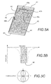
- FIG. 5A shows the active beam steering antenna of FIG. 4A configured being configured in a second mode, wherein the offset parasitic element is configured in a short circuit configuration when in the second mode.
- FIG. 5B shows a plot of the frequency response of the antenna of FIG. 5A when in the second mode.
- FIG. 5C shows a radiation pattern of the antenna of FIG. 5A when in the second mode.
- FIG. 6A shows the antenna of FIGS. 4A and 5A , with a tunable component being coupled to a feed junction of the antenna.
- FIG. 6B shows a plot of the frequency response of the antenna of FIG. 6A , as the offset parasitic element is switched between configuration modes (open circuit, short circuit) the tunable component is reconfigured to shift the frequency response of the antenna into the frequency band of interest.
- FIG. 6C shows a radiation pattern of the antenna of FIG. 6A in one mode.
- FIG. 7A shows an antenna similar to that shown in FIG. 6A , however, the tunable component is shown coupled to the second conductor for shifting a frequency response of the antenna.
- FIG. 7B shows a plot of the frequency response of the antenna of FIG. 7A , as the offset parasitic element is switched between configuration modes (open circuit, short circuit) the tunable component is reconfigured to shift the frequency response of the antenna into the frequency band of interest.
- FIG. 7C shows a radiation pattern of the antenna of FIG. 6A in one mode.
- FIGS. 8A-8B each shows an active beam steering antenna configured to adjust low band resonances of the antenna.
- FIG. 9 shows an alternative beam steering antenna configured for varying the low frequency resonance of the antenna system.
- FIG. 10 shows an antenna system wherein a planar parasitic conductor is implemented as the offset parasitic element to generate a beam steering function.
- FIG. 11 shows an antenna system wherein two planar conductors are implemented as offset parasitic elements to generate a beam steering function in the antenna at each of a low frequency band and a high frequency band.
- FIG. 12A shows an active beam steering antenna configured about a periphery of a wireless communication device.
- FIG. 12B shows a plot of the frequency response of the antenna of FIG. 12A in each of a first mode and a second mode.
- FIG. 13 illustrates a MIMO beam steering antenna system wherein the antenna system described in FIG. 12 is duplicated such that two of these antenna systems are co-located within the same device.
- FIG. 14 shows an active beam steering antenna having tuning slots between conductors, the tuning slots provide an overlapping region of the conductors that is confined within the conductor plane.
- FIG. 15 shows an active beam steering antenna with stacked rings.
- FIG. 16 shows another embodiment of an active beam steering antenna with stacked rings, the bottom and top rings can be grounded or ungrounded to alter the radiation mode of the antenna system.
- FIG. 17 shows a beam steering antenna system with an algorithm located in a processor, the algorithm accesses one or multiple metrics from the baseband of a communication system, the processor then implements a radiation mode selection process based upon one or multiple metrics from the baseband unit.
- FIG. 18 describes the functional use of a beam steering system in a mobile device in a cellular network wherein N radiation modes can be sampled and chosen from to improve the communication link quality between the mobile communication device and the Base Terminal.
- FIG. 19 shows a beam steering system and algorithm located in a processor, the algorithm accesses one or multiple metrics from the baseband of a communication system, the processor implements a radiation mode selection process based upon one or multiple metrics from the baseband unit, wherein control signals to drive the switches and tunable component are provided by the baseband/processor sub-system.
- three conductors are each positioned along the perimeter (or “periphery”) of a communication device to form an antenna system.
- One end of the first conductor is connected to a transceiver, with the transceiver providing an RF signal to the first conductor.
- a portion of the second conductor is positioned in proximity to a portion of the first conductor to form a first coupling region disposed therebetween. The characteristics of this first coupling region such as distance between conductors and length or amount of overlap of the conductors used to form this first coupling region are adjusted to control the resonant frequency and/or impedance properties of the antenna.
- the third conductor is positioned to form a second coupling region with the antenna formed by the first and second conductor, with this third conductor used to alter the current mode on the antenna.
- the third conductor can alter the current mode on the antenna formed by the first two conductors by short circuiting one end of the third conductor to ground or open circuit the third conductor. Transitioning from an open circuit condition to a short circuit condition on this third conductor will alter the current mode on the first and second conductors, resulting in an altering of the radiation pattern associated with the antenna.
- This third conductor is also referred to herein as an “offset parasitic element”.
- a switch can be used to connect or disconnect one end of the third conductor to ground.
- three conductors are positioned along the perimeter of a communication device to form an antenna system.
- One end of a first conductor of the three conductors is connected to a transceiver, with the transceiver providing an RF signal to the first conductor.
- a portion of the second conductor is positioned in proximity to a portion of the first conductor to form a first coupling region disposed therebetween. The characteristics of this first coupling region such as distance between conductors and length of overlap of the conductors forming this coupling region are adjusted to control the resonant frequency and/or impedance properties of the antenna.
- the space between the first and second conductors can be increased or decreased, and the length of overlapping portions of the first and second conductors can similarly be increased or decreased.
- the third conductor is positioned to form a second coupling region with the antenna formed by the first and second conductor, with this third conductor used to alter the current mode on the antenna.
- a multi-port switch can be connected to one end of the third conductor to provide additional impedances that can be connected between this end of the third conductor and the common ground.
- the impedance loads used to connect between the switch ports and the common ground can be chosen to provide additional radiation patterns from the single antenna formed by the first and second conductors.
- a tunable component such as a tunable capacitor can be implemented in a matching circuit at the feed point located at the junction of the first conductor and the transceiver port.
- the tunable component is configured to adjust the frequency response and/or impedance of the antenna system as the radiation modes are variably implemented. This tuning function is important to correct for frequency shifts that can be generated when the offset parasitic element used to alter current modes on the antenna elements switches or changes states.
- a fourth conductor can be implemented to form an additional coupling region such that two coupling regions are formed using three conductors positioned around the periphery of a device to form an antenna.
- the two coupling regions provide additional design flexibility in setting up additional frequency resonances from the antenna system.
- the fourth conductor can be used to couple to one or multiple regions of the three conductor antenna system to generate multiple radiation patterns by applying multiple impedance loads to this fourth conductor between one end of the conductor and the common ground.
- a three conductor antenna system as described above can be implemented around the perimeter of a communication device, and constrained to one half of the perimeter.
- a second antenna system of the same or similar design can be implemented around the perimeter of said communication device, with this second antenna system constrained to the half of the perimeter not occupied by the first antenna system.
- This two-antenna system with each antenna capable of beam steering, can be used for Multiple Input Multiple Output (MIMO) operation.
- MIMO Multiple Input Multiple Output
- the two-antenna systems can be used to implement a main antenna for 2G/3G cellular applications and the second antenna system used as a diversity antenna for 3G frequency bands.
- FIG. 1 illustrates an improved method of integrating an antenna external to a mobile device.
- An isolated magnetic dipole (IMD) antenna is formed which contains two coupled conductor sections 11 ; 12 , respectively; the first conductor 11 is used to form a low frequency resonance and the second conductor 12 is used to form a high frequency resonance.
- a tuning loop 15 is integrated internal to the mobile device, with the tuning loop coupled to the IMD antenna at the feed junction. The loop is used to feed the IMD antenna and can be adjusted to impedance match the IMD antenna to the transceiver.
- the internal loop is dimensioned such that the loop radiates or receives RF signals.
- the resonant frequency of the loop is adjusted such that the resonance is offset from the resonance of the external IMD antenna.
- An antenna encompassing the periphery of a device with integrated coupling regions for frequency control and to minimize effects of hand loading on antenna performance is shown.
- FIG. 2A illustrates an active beam steering antenna including a radiating element 21 positioned above a ground plane (circuit board) 26 forming an antenna volume therebetween, a first parasitic element 24 and a first active tuning element 25 coupled therewith is positioned within the antenna volume, and a second parasitic element 22 and second active tuning element 23 coupled therewith is positioned outside of the antenna volume and adjacent to the radiating element.
- a single resonance 27 having frequency f 0 is created when both parasitic elements 22 ; 24 are NOT shorted to ground. Dual resonances at f 0 and f 4 , respectively, are created when a parasitic element 22 is shorted to ground.
- Parasitic element 24 is then tuned to shift the frequency of the antenna f 0 into the band of interest.
- the parasitic and active tuning elements are tuned either by varactor diodes or variable elements that are voltage driven.
- a modal antenna capable of generating multiple radiation patterns from a single port antenna is shown.
- FIG. 2C shows a first radiation pattern associated with the active beam steering antenna.
- FIG. 2D shows a second radiation pattern associated with the active beam steering antenna.
- FIGS. 2 A-D
- the active beam steering antenna of FIGS. 2 (A-D) is further described in commonly owned U.S. Pat. No. 7,911,402, issued Mar. 22, 2011, the contents of which is hereby incorporated by reference.
- FIGS. 3 illustrate an improvement in bandwidth achieved when an additional conductor is coupled to an external IMD antenna.
- An additional resonance at the upper frequency band can be generated by coupling an additional conductor to one of the conductors in the IMD antenna. The coupling of the additional conductor effectuates a change in frequency response of the antenna.
- an additional conductor can be applied to generate another coupling region for frequency control.
- a tunable component can be added to develop an embodiment which tunes the frequency response.
- the antenna includes a first conductor 121 and a second conductor 122 collectively extending about a periphery 120 of the wireless communication device.
- An offset parasitic element 123 is positioned near a first coupling region (region of overlap of the first and second conductors) and connected to ground.
- An active tunable component 125 and a tuning loop 124 are each coupled to a feed junction of the antenna.
- FIG. 3B shows the frequency response of the antenna of FIG. 3A , wherein the offset parasitic element forms a split resonance in the high band.
- FIG. 4 illustrates an antenna system comprised of four conductors, three of which are positioned around the periphery of a ground plane associated with a wireless communication device.
- a first conductor 41 is fed with a signal source and the first end of a second conductor 42 is positioned such that a region of the second conductor forms a first coupling region 49 a with a portion of the first conductor.
- the second end of the second conductor is grounded to the ground plane 44 .
- a third conductor 43 is positioned to form a second coupling region 49 b with the second conductor at a region of overlap therebetween, with this third conductor traversing the remainder of the perimeter of the ground plane.
- a fourth conductor 46 provides the offset parasitic and is positioned in proximity to the first coupling region formed by the first and second conductors.
- This offset parasitic element 46 is not ground to the ground plane or connected to any other features in this antenna system, thus the antenna is said to be configured in a “first mode”.
- FIG. 4B a frequency response of the antenna is shown along with a frequency band of interest 48 .
- FIG. 4C a two dimensional representation of the radiation pattern of the antenna formed by these four conductors at the resonant frequency.
- FIG. 5 illustrates the antenna system described in FIG. 4 with the exception that the offset parasitic is grounded to the ground plane and the antenna is said to be in a “second mode”.
- the antenna includes a first conductor 41 , and second conductor 42 overlapping at first coupling region 49 a .
- a third conductor 43 overlaps with the second conductor 42 at a second coupling region 49 b .
- the first through third conductors expand about the perimeter of a circuit board 44 .
- a feed and tuning circuit 45 is coupled to the first conductor.
- Offset parasitic element 46 is shown with a connection 47 b coupling to ground.
- FIG. 5B shows a split resonant frequency response associated with the antenna system of FIG. 5A .
- FIG. 5C shows a two dimensional representation of the radiation pattern of the antenna formed by these four conductors at the resonant frequency.
- the radiation pattern has rotated with respect to the radiation pattern shown in FIG. 4C , with this pattern rotation due to the connecting of the offset parasitic to the ground plane.
- FIG. 6 illustrates the antenna system described in FIG. 4 with the exceptions of one port of a switch 61 connected to one end of the offset parasitic 46 , with the second port of the switch 61 connected to the ground plane 44 .
- a second exception is that a tunable component 62 is connected in shunt to the signal source feeding the antenna at the junction 63 with the first conductor 41 . Otherwise, the components are similar to that of the antenna in FIG. 4A . Thus, here a tunable component is used to shift the antenna frequency response lower to provide a good return loss in the frequency band of interest.
- FIG. 6B shows the frequency response of the antenna system before and after tuning using the tunable component.
- a frequency band of interest 48 is shown, along with the radiation pattern of the antenna in the first mode 64 and that of the antenna in the second mode 65 .
- the radiation pattern is the same as shown in FIG. 5 .
- FIG. 7A illustrates the antenna system described in FIG. 6 with the exception that the tunable component used in shunt with the signal source feeding the antenna has been moved wherein one end of the tunable component 62 is connected to the second end of the second conductor, with the other port of the tunable component connected to the ground plane.
- the tuning circuit and feed 45 are coupled to the first conductor.
- Switch 61 is shown for coupling and decoupling the offset parasitic element to ground. Accordingly, an alternative method is shown for shifting the frequency response lower to provide a good return loss in the frequency band of interest.
- FIG. 7B shows the frequency response of the antenna system of FIG. 7A before and after tuning using the tunable component 62 .
- FIG. 7C the radiation pattern is the same as shown in FIG. 6C .
- FIGS. 8 illustrate two methods of beam steering at the low frequency resonance formed by the antenna system.
- the first method referring to the antenna of FIG. 8A , shows an extended offset parasitic 46 a in an “L” shape, which allows for a longer coupling region between the parasitic element and the first and second conductors 41 ; 42 , respectively.
- the offset parasitic element is coupled to a switch 61 a for connecting and disconnecting the parasitic element to ground 44 .
- the tuning and feed circuit 45 is coupled to the first conductor 41 .
- the tunable component 62 is shown coupled to the second conductor 42 .
- a third conductor 43 along with the first and second conductors are configured to extend about a perimeter of the device or circuit board.
- the second method shows a pair of offset parasitic elements 46 b ; 46 c , one designated for “high frequency bands” and the other designated “low frequency bands”. These two offset parasitic elements can be optimized for low band and high band operation. Each is coupled to a respective switch 61 b ; 61 c . the remainder of the antenna is similar in configuration to that shown in FIG. 8A .
- FIG. 9 illustrates an alternate scheme for beam steering (or “null steering”) at the low frequency resonance of the antenna system.
- This method is similar to the first method illustrated in FIG. 8 with the exception that the third conductor shown in FIG. 8 has been separated into two conductors, a third conductor 93 and fourth conductor 94 here in FIG. 9 .
- One end of the third conductor is positioned in proximity to a portion of the second conductor 92 and forms a second coupling region with this second conductor.
- the opposing end of the third conductor is grounded to the ground plane 44 .
- the fourth conductor is positioned to traverse the remainder of the periphery of the ground plane.
- the first coupling region is formed between the overlapping first conductor 91 and second conductor 92 .
- a tuning and feed circuit 45 is coupled to the first conductor 91 .
- the offset parasitic element 46 is coupled to a switch 61 for connecting and disconnecting to the ground plane 44 .
- FIG. 10 illustrates an antenna system wherein a planar conductor is implemented as an offset parasitic element 101 to generate a beam steering function. Otherwise, the antenna system of FIG. 10 is similar to the embodiment as illustrated in FIG. 6 .
- FIG. 11 illustrates an antenna system wherein two planar conductors 101 ; 111 are implemented as offset parasitic elements to generate a beam steering function at a low frequency band and a high frequency band.
- the first offset parasitic element 101 is coupled to a first switch 61 which is further coupled to ground.
- the second offset parasitic element 111 is coupled to a second switch 112 which is further coupled to ground.
- the first and second parasitic elements are configured to produce low band and high band resonances, with the first offset parasitic element as shown being configured for the high band resonance and the second offset parasitic element as shown being configured for the low band resonance.
- FIGS. 12 illustrate a scheme for beam steering at both a low frequency and a high frequency by implementing an offset parasitic element which has a section of conductor which is shaped to bend back to increase the physical length of conductor within a confined area.
- the single offset parasitic element 121 couples to two coupling regions formed by the first, second, and third conductors 41 ; 42 ; 43 , respectively, that are used to form an antenna. Otherwise, the antenna is structured and configured similar to that of FIG. 9 .
- FIG. 12B shows a frequency response of the antenna of FIG. 12A , wherein both the low and high frequency band resonances are shown for both the open circuited 122 and short circuited 123 states for the offset parasitic. Frequency bands of interest 121 in the low band and high bands are shown.
- FIG. 13 illustrates a MIMO beam steering antenna system wherein the antenna system described in FIG. 12 is duplicated such that two of these antenna systems are co-located within the same device, the device in this case shown being a common ground plane.
- FIG. 14 illustrates a beam steering antenna system wherein the conductor used to form the antenna is in a planar fashion.
- the conductors are cut to form an overlap region in the conductor plane.
- the conductors are configured with slotted regions for creating an overlap.
- the length, thickness, and space between conductors can be configured for optimizing the performance of the antenna.
- the antenna comprises a first conductor 141 , a second conductor 142 , and a third conductor 143 extending about a periphery of the device circuit board 148 .
- An active tunable component 146 is coupled to a feed 147 and tuning circuit, which is further coupled to the first conductor.
- An offset parasitic element 144 is coupled to a switch 145 which is further coupled to ground 148 .
- FIG. 15 illustrates a beam steering antenna system wherein two conductors are stacked to form a two conductor assembly. Both conductors are planar, with one conductor fed with an RF signal with this conductor forming the radiating element.
- the second conductor is positioned above the first conductor, with this second conductor containing a fixed ground point and a switch.
- the switch provides a method of dynamically grounding or un-grounding the second conductor to the common ground plane.
- stacked rings are in planar alignment, a switch is coupled to the bottom ring to connect and disconnect the second ring from the ground plane.
- the antenna includes a first conductor 151 , a second conductor 152 and a third conductor 153 extending about a periphery of the device forming a first ring.
- a second ring includes a fourth conductor 154 .
- the first ring is positioned above the second ring about the periphery.
- a tuning and feed circuit is coupled to the first conductor with a tunable component 158 coupled therewith.
- An offset parasitic element 155 is coupled to a switch 156 which is further coupled to ground 159 .
- a second switch 157 is used to couple and disconnect the second ring to the ground plane 159 .
- FIG. 16 illustrates a beam steering antenna system wherein three rings are stacked to form a three ring assembly. All three rings are planar, with one conductor fed with an RF signal with this conductor forming the radiating element. The two additional rings are positioned above and below the first ring, with these additional two rings containing fixed ground points and switches 167 ; 168 . The switches provide a method of dynamically grounding or un-grounding the two additional conductors to the common ground plane.
- FIG. 17 illustrates a beam steering system along with an algorithm located in a processor.
- the algorithm accesses one or multiple metrics from the baseband of a communication system, with these metrics being Channel Quality Indicator (CQI), Receive Signal Strength Indicator (RSSI), Signal to Interference and Noise Ratio (SINR), or other metric.
- CQI Channel Quality Indicator
- RSSI Receive Signal Strength Indicator
- SINR Signal to Interference and Noise Ratio
- the algorithm in the processor implements a radiation mode selection process based upon one or multiple metrics from the baseband unit.
- FIG. 18 describes the functional use of a beam steering system in a mobile device in a cellular network wherein N radiation modes can be sampled and chosen from to improve the communication link quality between the mobile communication device and the Base Terminal.
- FIG. 19 illustrates a beam steering system along with an algorithm located in a processor.
- the algorithm accesses one or multiple metrics from the baseband of a communication system, with these metrics being Channel Quality Indicator (CQI), Receive Signal Strength Indicator (RSSI), Signal to Interference and Noise Ratio (SINR), or other metric.
- CQI Channel Quality Indicator
- RSSI Receive Signal Strength Indicator
- SINR Signal to Interference and Noise Ratio
- the algorithm in the processor implements a radiation mode selection process based upon one or multiple metrics from the baseband unit. Control signals to drive the switches and tunable component are provided by the Baseband/Processor sub-system.
Landscapes
- Engineering & Computer Science (AREA)
- Computer Networks & Wireless Communication (AREA)
- Signal Processing (AREA)
- Variable-Direction Aerials And Aerial Arrays (AREA)
Abstract
Description
Claims (26)
Priority Applications (1)
| Application Number | Priority Date | Filing Date | Title |
|---|---|---|---|
| US14/930,651 US10033097B2 (en) | 2008-03-05 | 2015-11-02 | Integrated antenna beam steering system |
Applications Claiming Priority (8)
| Application Number | Priority Date | Filing Date | Title |
|---|---|---|---|
| US12/043,090 US7911402B2 (en) | 2008-03-05 | 2008-03-05 | Antenna and method for steering antenna beam direction |
| US13/029,564 US8362962B2 (en) | 2008-03-05 | 2011-02-17 | Antenna and method for steering antenna beam direction |
| US201161532822P | 2011-09-09 | 2011-09-09 | |
| US13/609,138 US9859617B1 (en) | 2011-09-09 | 2012-09-10 | Active antenna structure maximizing aperture and anchoring RF behavior |
| US13/726,477 US8648755B2 (en) | 2008-03-05 | 2012-12-24 | Antenna and method for steering antenna beam direction |
| US14/144,461 US9240634B2 (en) | 2007-08-17 | 2013-12-30 | Antenna and method for steering antenna beam direction |
| US201462073609P | 2014-10-31 | 2014-10-31 | |
| US14/930,651 US10033097B2 (en) | 2008-03-05 | 2015-11-02 | Integrated antenna beam steering system |
Related Parent Applications (2)
| Application Number | Title | Priority Date | Filing Date |
|---|---|---|---|
| US13/609,138 Continuation-In-Part US9859617B1 (en) | 2008-03-05 | 2012-09-10 | Active antenna structure maximizing aperture and anchoring RF behavior |
| US14/144,461 Continuation-In-Part US9240634B2 (en) | 2007-08-17 | 2013-12-30 | Antenna and method for steering antenna beam direction |
Related Child Applications (1)
| Application Number | Title | Priority Date | Filing Date |
|---|---|---|---|
| US14/144,461 Continuation US9240634B2 (en) | 2007-08-17 | 2013-12-30 | Antenna and method for steering antenna beam direction |
Publications (2)
| Publication Number | Publication Date |
|---|---|
| US20160190685A1 US20160190685A1 (en) | 2016-06-30 |
| US10033097B2 true US10033097B2 (en) | 2018-07-24 |
Family
ID=56165358
Family Applications (1)
| Application Number | Title | Priority Date | Filing Date |
|---|---|---|---|
| US14/930,651 Active 2029-05-02 US10033097B2 (en) | 2008-03-05 | 2015-11-02 | Integrated antenna beam steering system |
Country Status (1)
| Country | Link |
|---|---|
| US (1) | US10033097B2 (en) |
Cited By (1)
| Publication number | Priority date | Publication date | Assignee | Title |
|---|---|---|---|---|
| US10297906B2 (en) * | 2017-05-02 | 2019-05-21 | Lg Electronics Inc. | Mobile terminal |
Families Citing this family (3)
| Publication number | Priority date | Publication date | Assignee | Title |
|---|---|---|---|---|
| CN107181045B (en) * | 2017-06-19 | 2024-02-20 | 上海传英信息技术有限公司 | Antenna of mobile terminal and mobile terminal with same |
| CN111052501B (en) * | 2018-05-08 | 2021-10-22 | 华为技术有限公司 | Antenna device and mobile terminal |
| CN115775973A (en) * | 2021-09-07 | 2023-03-10 | 富泰京精密电子(烟台)有限公司 | Antenna structure and wireless communication device with same |
Citations (35)
| Publication number | Priority date | Publication date | Assignee | Title |
|---|---|---|---|---|
| US2236102A (en) | 1938-04-28 | 1941-03-25 | Internat Telephone Dev Co Inc | High frequency wave transmission system |
| US2761134A (en) | 1952-01-18 | 1956-08-28 | Bendix Aviat Corp | Means for operating antennas |
| US3971031A (en) | 1975-10-31 | 1976-07-20 | Burke Emmett F | Loaded quad antenna |
| US5235343A (en) | 1990-08-21 | 1993-08-10 | Societe D'etudes Et De Realisation De Protection Electronique Informatique Electronique | High frequency antenna with a variable directing radiation pattern |
| US5568155A (en) | 1992-12-07 | 1996-10-22 | Ntt Mobile Communications Network Incorporation | Antenna devices having double-resonance characteristics |
| US5598169A (en) | 1995-03-24 | 1997-01-28 | Lucent Technologies Inc. | Detector and modulator circuits for passive microwave links |
| US5777581A (en) | 1995-12-07 | 1998-07-07 | Atlantic Aerospace Electronics Corporation | Tunable microstrip patch antennas |
| US5874919A (en) | 1997-01-09 | 1999-02-23 | Harris Corporation | Stub-tuned, proximity-fed, stacked patch antenna |
| US5943016A (en) | 1995-12-07 | 1999-08-24 | Atlantic Aerospace Electronics, Corp. | Tunable microstrip patch antenna and feed network therefor |
| US6198943B1 (en) * | 1999-05-17 | 2001-03-06 | Ericsson Inc. | Parasitic dual band matching of an internal looped dipole antenna |
| US6326921B1 (en) | 2000-03-14 | 2001-12-04 | Telefonaktiebolaget Lm Ericsson (Publ) | Low profile built-in multi-band antenna |
| US20040027286A1 (en) | 2001-06-26 | 2004-02-12 | Gregory Poilasne | Multi frequency magnetic dipole antenna structures and methods of reusing the volume of an antenna |
| US6765536B2 (en) | 2002-05-09 | 2004-07-20 | Motorola, Inc. | Antenna with variably tuned parasitic element |
| US20040227667A1 (en) | 2003-05-12 | 2004-11-18 | Hrl Laboratories, Llc | Meta-element antenna and array |
| US6876329B2 (en) * | 2002-08-30 | 2005-04-05 | Filtronic Lk Oy | Adjustable planar antenna |
| US6903686B2 (en) | 2002-12-17 | 2005-06-07 | Sony Ericsson Mobile Communications Ab | Multi-branch planar antennas having multiple resonant frequency bands and wireless terminals incorporating the same |
| US20050192727A1 (en) | 1994-05-09 | 2005-09-01 | Automotive Technologies International Inc. | Sensor Assemblies |
| US20050275596A1 (en) | 2004-06-14 | 2005-12-15 | Nec Corporation | Antenna device and portable radio terminal |
| US20050285541A1 (en) | 2003-06-23 | 2005-12-29 | Lechevalier Robert E | Electron beam RF amplifier and emitter |
| US7081854B2 (en) | 2002-05-02 | 2006-07-25 | Sony Ericsson Mobile Communications Ab | Printed built-in antenna for use in a portable electronic communication apparatus |
| US20060220966A1 (en) | 2005-03-29 | 2006-10-05 | Ethertronics | Antenna element-counterpoise arrangement in an antenna |
| US7132989B1 (en) | 2005-05-04 | 2006-11-07 | Kyocera Wireless Corp. | Apparatus, system, and method for adjusting antenna characteristics using tunable parasitic elements |
| US7180464B2 (en) | 2004-07-29 | 2007-02-20 | Interdigital Technology Corporation | Multi-mode input impedance matching for smart antennas and associated methods |
| US20070069958A1 (en) | 2005-09-29 | 2007-03-29 | Sony Ericsson Mobile Communications Ab | Multi-band bent monopole antenna |
| US20070176824A1 (en) | 2002-09-30 | 2007-08-02 | Nanosys Inc. | Phased array systems and methods |
| US7265720B1 (en) * | 2006-12-29 | 2007-09-04 | Motorola, Inc. | Planar inverted-F antenna with parasitic conductor loop and device using same |
| US20080001829A1 (en) | 2006-06-30 | 2008-01-03 | Nokia Corporation | Mechanically tunable antenna for communication devices |
| US7330156B2 (en) | 2004-08-20 | 2008-02-12 | Nokia Corporation | Antenna isolation using grounded microwave elements |
| US7528783B2 (en) * | 2007-01-15 | 2009-05-05 | Panasonic Corporation | Antenna |
| US7728785B2 (en) * | 2006-02-07 | 2010-06-01 | Nokia Corporation | Loop antenna with a parasitic radiator |
| US7830320B2 (en) | 2007-08-20 | 2010-11-09 | Ethertronics, Inc. | Antenna with active elements |
| US7903034B2 (en) | 2005-09-19 | 2011-03-08 | Fractus, S.A. | Antenna set, portable wireless device, and use of a conductive element for tuning the ground-plane of the antenna set |
| US7911402B2 (en) | 2008-03-05 | 2011-03-22 | Ethertronics, Inc. | Antenna and method for steering antenna beam direction |
| US9444130B2 (en) * | 2013-04-10 | 2016-09-13 | Apple Inc. | Antenna system with return path tuning and loop element |
| US9711858B1 (en) * | 2013-02-28 | 2017-07-18 | Amazon Technologies, Inc. | Impedance-controlled dual-feed antenna |
-
2015
- 2015-11-02 US US14/930,651 patent/US10033097B2/en active Active
Patent Citations (36)
| Publication number | Priority date | Publication date | Assignee | Title |
|---|---|---|---|---|
| US2236102A (en) | 1938-04-28 | 1941-03-25 | Internat Telephone Dev Co Inc | High frequency wave transmission system |
| US2761134A (en) | 1952-01-18 | 1956-08-28 | Bendix Aviat Corp | Means for operating antennas |
| US3971031A (en) | 1975-10-31 | 1976-07-20 | Burke Emmett F | Loaded quad antenna |
| US5235343A (en) | 1990-08-21 | 1993-08-10 | Societe D'etudes Et De Realisation De Protection Electronique Informatique Electronique | High frequency antenna with a variable directing radiation pattern |
| US5568155A (en) | 1992-12-07 | 1996-10-22 | Ntt Mobile Communications Network Incorporation | Antenna devices having double-resonance characteristics |
| US20050192727A1 (en) | 1994-05-09 | 2005-09-01 | Automotive Technologies International Inc. | Sensor Assemblies |
| US5598169A (en) | 1995-03-24 | 1997-01-28 | Lucent Technologies Inc. | Detector and modulator circuits for passive microwave links |
| US5777581A (en) | 1995-12-07 | 1998-07-07 | Atlantic Aerospace Electronics Corporation | Tunable microstrip patch antennas |
| US5943016A (en) | 1995-12-07 | 1999-08-24 | Atlantic Aerospace Electronics, Corp. | Tunable microstrip patch antenna and feed network therefor |
| US5874919A (en) | 1997-01-09 | 1999-02-23 | Harris Corporation | Stub-tuned, proximity-fed, stacked patch antenna |
| US6198943B1 (en) * | 1999-05-17 | 2001-03-06 | Ericsson Inc. | Parasitic dual band matching of an internal looped dipole antenna |
| US6326921B1 (en) | 2000-03-14 | 2001-12-04 | Telefonaktiebolaget Lm Ericsson (Publ) | Low profile built-in multi-band antenna |
| US20040027286A1 (en) | 2001-06-26 | 2004-02-12 | Gregory Poilasne | Multi frequency magnetic dipole antenna structures and methods of reusing the volume of an antenna |
| US7081854B2 (en) | 2002-05-02 | 2006-07-25 | Sony Ericsson Mobile Communications Ab | Printed built-in antenna for use in a portable electronic communication apparatus |
| US6765536B2 (en) | 2002-05-09 | 2004-07-20 | Motorola, Inc. | Antenna with variably tuned parasitic element |
| US6876329B2 (en) * | 2002-08-30 | 2005-04-05 | Filtronic Lk Oy | Adjustable planar antenna |
| US20070176824A1 (en) | 2002-09-30 | 2007-08-02 | Nanosys Inc. | Phased array systems and methods |
| US6903686B2 (en) | 2002-12-17 | 2005-06-07 | Sony Ericsson Mobile Communications Ab | Multi-branch planar antennas having multiple resonant frequency bands and wireless terminals incorporating the same |
| US20040227667A1 (en) | 2003-05-12 | 2004-11-18 | Hrl Laboratories, Llc | Meta-element antenna and array |
| US7068234B2 (en) | 2003-05-12 | 2006-06-27 | Hrl Laboratories, Llc | Meta-element antenna and array |
| US20050285541A1 (en) | 2003-06-23 | 2005-12-29 | Lechevalier Robert E | Electron beam RF amplifier and emitter |
| US20050275596A1 (en) | 2004-06-14 | 2005-12-15 | Nec Corporation | Antenna device and portable radio terminal |
| US7180464B2 (en) | 2004-07-29 | 2007-02-20 | Interdigital Technology Corporation | Multi-mode input impedance matching for smart antennas and associated methods |
| US7330156B2 (en) | 2004-08-20 | 2008-02-12 | Nokia Corporation | Antenna isolation using grounded microwave elements |
| US20060220966A1 (en) | 2005-03-29 | 2006-10-05 | Ethertronics | Antenna element-counterpoise arrangement in an antenna |
| US7132989B1 (en) | 2005-05-04 | 2006-11-07 | Kyocera Wireless Corp. | Apparatus, system, and method for adjusting antenna characteristics using tunable parasitic elements |
| US7903034B2 (en) | 2005-09-19 | 2011-03-08 | Fractus, S.A. | Antenna set, portable wireless device, and use of a conductive element for tuning the ground-plane of the antenna set |
| US20070069958A1 (en) | 2005-09-29 | 2007-03-29 | Sony Ericsson Mobile Communications Ab | Multi-band bent monopole antenna |
| US7728785B2 (en) * | 2006-02-07 | 2010-06-01 | Nokia Corporation | Loop antenna with a parasitic radiator |
| US20080001829A1 (en) | 2006-06-30 | 2008-01-03 | Nokia Corporation | Mechanically tunable antenna for communication devices |
| US7265720B1 (en) * | 2006-12-29 | 2007-09-04 | Motorola, Inc. | Planar inverted-F antenna with parasitic conductor loop and device using same |
| US7528783B2 (en) * | 2007-01-15 | 2009-05-05 | Panasonic Corporation | Antenna |
| US7830320B2 (en) | 2007-08-20 | 2010-11-09 | Ethertronics, Inc. | Antenna with active elements |
| US7911402B2 (en) | 2008-03-05 | 2011-03-22 | Ethertronics, Inc. | Antenna and method for steering antenna beam direction |
| US9711858B1 (en) * | 2013-02-28 | 2017-07-18 | Amazon Technologies, Inc. | Impedance-controlled dual-feed antenna |
| US9444130B2 (en) * | 2013-04-10 | 2016-09-13 | Apple Inc. | Antenna system with return path tuning and loop element |
Cited By (2)
| Publication number | Priority date | Publication date | Assignee | Title |
|---|---|---|---|---|
| US10297906B2 (en) * | 2017-05-02 | 2019-05-21 | Lg Electronics Inc. | Mobile terminal |
| US10658733B2 (en) * | 2017-05-02 | 2020-05-19 | Lg Electronics Inc. | Mobile terminal |
Also Published As
| Publication number | Publication date |
|---|---|
| US20160190685A1 (en) | 2016-06-30 |
Similar Documents
| Publication | Publication Date | Title |
|---|---|---|
| US20220231418A1 (en) | Reconfigurable Multi-Mode Active Antenna System | |
| US9660348B2 (en) | Multi-function array for access point and mobile wireless systems | |
| US8988289B2 (en) | Antenna system for interference supression | |
| US9680514B2 (en) | Methods for reducing near-field radiation and specific absorption rate (SAR) values in communications devices | |
| US9755305B2 (en) | Active antenna adapted for impedance matching and band switching using a shared component | |
| US7688275B2 (en) | Multimode antenna structure | |
| US9160074B2 (en) | Modal antenna with correlation management for diversity applications | |
| US8780002B2 (en) | Multiple-input multiple-output (MIMO) multi-band antennas with a conductive neutralization line for signal decoupling | |
| KR101475295B1 (en) | multimode antenna structure | |
| US6900773B2 (en) | Active configurable capacitively loaded magnetic diploe | |
| JP3211445U (en) | Modal antenna with correlation adjustment for diversity applications | |
| US20130120200A1 (en) | Multi leveled active antenna configuration for multiband mimo lte system | |
| KR20130125361A (en) | Smart antenna for wireless communications | |
| US10033097B2 (en) | Integrated antenna beam steering system | |
| KR20120015352A (en) | Methods for reducing near-field radiation and specific absorption rate(sar) values in communications devices | |
| US9654230B2 (en) | Modal adaptive antenna for mobile applications | |
| US9634404B1 (en) | Beam steering multiband architecture | |
| US20190214723A1 (en) | Beam-steerable antenna devices, systems, and methods | |
| US9692122B2 (en) | Multi leveled active antenna configuration for multiband MIMO LTE system |
Legal Events
| Date | Code | Title | Description |
|---|---|---|---|
| AS | Assignment |
Owner name: NH EXPANSION CREDIT FUND HOLDINGS LP, NEW YORK Free format text: SECURITY INTEREST;ASSIGNOR:ETHERTRONICS, INC.;REEL/FRAME:040464/0245 Effective date: 20161013 |
|
| AS | Assignment |
Owner name: ETHERTRONICS, INC., CALIFORNIA Free format text: ASSIGNMENT OF ASSIGNORS INTEREST;ASSIGNORS:DESCLOS, LAURENT;SINGH, ABHISHEK;SHAMBLIN, JEFFREY;SIGNING DATES FROM 20170321 TO 20170327;REEL/FRAME:042108/0202 |
|
| AS | Assignment |
Owner name: SILICON VALLEY BANK, CALIFORNIA Free format text: SECURITY INTEREST;ASSIGNOR:ETHERTRONICS, INC.;REEL/FRAME:044106/0829 Effective date: 20080911 |
|
| AS | Assignment |
Owner name: ETHERTRONICS, INC., CALIFORNIA Free format text: RELEASE BY SECURED PARTY;ASSIGNOR:NH EXPANSION CREDIT FUND HOLDINGS LP;REEL/FRAME:045210/0725 Effective date: 20180131 |
|
| FEPP | Fee payment procedure |
Free format text: ENTITY STATUS SET TO UNDISCOUNTED (ORIGINAL EVENT CODE: BIG.); ENTITY STATUS OF PATENT OWNER: LARGE ENTITY |
|
| STCF | Information on status: patent grant |
Free format text: PATENTED CASE |
|
| MAFP | Maintenance fee payment |
Free format text: PAYMENT OF MAINTENANCE FEE, 4TH YEAR, LARGE ENTITY (ORIGINAL EVENT CODE: M1551); ENTITY STATUS OF PATENT OWNER: LARGE ENTITY Year of fee payment: 4 |
|
| AS | Assignment |
Owner name: KYOCERA AVX COMPONENTS (SAN DIEGO), INC., CALIFORNIA Free format text: CHANGE OF NAME;ASSIGNOR:AVX ANTENNA, INC.;REEL/FRAME:063543/0302 Effective date: 20211001 |
|
| AS | Assignment |
Owner name: AVX ANTENNA, INC., CALIFORNIA Free format text: CHANGE OF NAME;ASSIGNOR:ETHERTRONICS, INC.;REEL/FRAME:063549/0336 Effective date: 20180206 |