US10027358B2 - Harmonic selective full-band capture receiver with digital harmonic rejection calibration - Google Patents
Harmonic selective full-band capture receiver with digital harmonic rejection calibration Download PDFInfo
- Publication number
- US10027358B2 US10027358B2 US15/240,344 US201615240344A US10027358B2 US 10027358 B2 US10027358 B2 US 10027358B2 US 201615240344 A US201615240344 A US 201615240344A US 10027358 B2 US10027358 B2 US 10027358B2
- Authority
- US
- United States
- Prior art keywords
- harmonic
- spectrum segments
- circuitry
- tias
- received signal
- Prior art date
- Legal status (The legal status is an assumption and is not a legal conclusion. Google has not performed a legal analysis and makes no representation as to the accuracy of the status listed.)
- Active, expires
Links
Images


Classifications
-
- H—ELECTRICITY
- H03—ELECTRONIC CIRCUITRY
- H03D—DEMODULATION OR TRANSFERENCE OF MODULATION FROM ONE CARRIER TO ANOTHER
- H03D7/00—Transference of modulation from one carrier to another, e.g. frequency-changing
- H03D7/16—Multiple-frequency-changing
- H03D7/165—Multiple-frequency-changing at least two frequency changers being located in different paths, e.g. in two paths with carriers in quadrature
-
- H—ELECTRICITY
- H04—ELECTRIC COMMUNICATION TECHNIQUE
- H04B—TRANSMISSION
- H04B1/00—Details of transmission systems, not covered by a single one of groups H04B3/00 - H04B13/00; Details of transmission systems not characterised by the medium used for transmission
- H04B1/06—Receivers
- H04B1/10—Means associated with receiver for limiting or suppressing noise or interference
- H04B1/109—Means associated with receiver for limiting or suppressing noise or interference by improving strong signal performance of the receiver when strong unwanted signals are present at the receiver input
-
- H—ELECTRICITY
- H03—ELECTRONIC CIRCUITRY
- H03D—DEMODULATION OR TRANSFERENCE OF MODULATION FROM ONE CARRIER TO ANOTHER
- H03D7/00—Transference of modulation from one carrier to another, e.g. frequency-changing
- H03D7/14—Balanced arrangements
- H03D7/1425—Balanced arrangements with transistors
- H03D7/1466—Passive mixer arrangements
-
- H—ELECTRICITY
- H04—ELECTRIC COMMUNICATION TECHNIQUE
- H04B—TRANSMISSION
- H04B1/00—Details of transmission systems, not covered by a single one of groups H04B3/00 - H04B13/00; Details of transmission systems not characterised by the medium used for transmission
- H04B1/06—Receivers
- H04B1/10—Means associated with receiver for limiting or suppressing noise or interference
- H04B1/1018—Means associated with receiver for limiting or suppressing noise or interference noise filters connected between the power supply and the receiver
-
- H—ELECTRICITY
- H04—ELECTRIC COMMUNICATION TECHNIQUE
- H04B—TRANSMISSION
- H04B1/00—Details of transmission systems, not covered by a single one of groups H04B3/00 - H04B13/00; Details of transmission systems not characterised by the medium used for transmission
- H04B1/06—Receivers
- H04B1/10—Means associated with receiver for limiting or suppressing noise or interference
- H04B1/1027—Means associated with receiver for limiting or suppressing noise or interference assessing signal quality or detecting noise/interference for the received signal
- H04B1/1036—Means associated with receiver for limiting or suppressing noise or interference assessing signal quality or detecting noise/interference for the received signal with automatic suppression of narrow band noise or interference, e.g. by using tuneable notch filters
-
- H—ELECTRICITY
- H03—ELECTRONIC CIRCUITRY
- H03D—DEMODULATION OR TRANSFERENCE OF MODULATION FROM ONE CARRIER TO ANOTHER
- H03D2200/00—Indexing scheme relating to details of demodulation or transference of modulation from one carrier to another covered by H03D
- H03D2200/0041—Functional aspects of demodulators
- H03D2200/0066—Mixing
- H03D2200/0074—Mixing using a resistive mixer or a passive mixer
-
- H—ELECTRICITY
- H03—ELECTRONIC CIRCUITRY
- H03D—DEMODULATION OR TRANSFERENCE OF MODULATION FROM ONE CARRIER TO ANOTHER
- H03D2200/00—Indexing scheme relating to details of demodulation or transference of modulation from one carrier to another covered by H03D
- H03D2200/0041—Functional aspects of demodulators
- H03D2200/0086—Reduction or prevention of harmonic frequencies
-
- H04W4/008—
-
- H—ELECTRICITY
- H04—ELECTRIC COMMUNICATION TECHNIQUE
- H04W—WIRELESS COMMUNICATION NETWORKS
- H04W4/00—Services specially adapted for wireless communication networks; Facilities therefor
- H04W4/80—Services using short range communication, e.g. near-field communication [NFC], radio-frequency identification [RFID] or low energy communication
Definitions
- the present disclosure is directed to radio frequency (RF) receivers and more specifically to RF receiver front ends.
- RF radio frequency
- Wideband receivers are configured to provide filtering to most out-of-band blocker signals before any baseband amplification.
- Wideband receivers can employ passive mixers that immediately down-convert an input current to baseband.
- a transimpedance amplifier (TIA) then converts any baseband current in the receive band to voltage.
- RF radio frequency
- RF radio frequency
- FIG. 1 is a block diagram of an exemplary wireless communication device
- FIG. 2A illustrates exemplary graphs of local oscillator (LO) signal and gain waveforms for a mixer
- FIG. 2B illustrates exemplary graphs LO signal and gain waveforms for a mixer
- FIG. 3A is a diagram of a mixer with associated LO clock waveforms
- FIG. 3B illustrates exemplary graphs of LO signal waveforms for a mixer
- FIG. 4 is an exemplary diagram of a receiver front end
- FIG. 5A illustrates an exemplary diagram of a portion of a harmonic selective full band capture (FBC) receiver front end
- FIG. 5B illustrates exemplary graphs of LO signal and gain waveforms for a harmonic selective FBC receiver front end
- FIG. 6 illustrates exemplary graphs of LO signal and gain waveforms for a harmonic selective FBC receiver front end
- FIG. 7 illustrates exemplary graphs of LO signal and gain waveforms for a harmonic selective FBC receiver front end
- FIG. 8 is an exemplary diagram of a harmonic selective FBC receiver front end
- FIG. 9 is an exemplary diagram of a harmonic selective FBC receiver front end
- FIG. 10 illustrates exemplary graphs of gain and noise figure for a harmonic selective FBC receiver
- FIG. 11A illustrates exemplary graphs of gain and noise figure for a harmonic selective FBC receiver
- FIG. 11B illustrates exemplary graphs of gain and noise figure for a harmonic selective FBC receiver
- FIG. 12 is an exemplary flowchart of a process for selecting and processing one or more spectrum segments of a harmonic selective FBC receiver.
- FIG. 13 is an exemplary flowchart of a process for performing calibration of a harmonic selective FBC receiver.
- a device includes circuitry configured to determine one or more first local oscillator (LO) harmonics that correspond to one or more first spectrum segments of a down-converted received signal based on characteristics of the received signal.
- the one or more first LO harmonics of the received signal are amplified by applying one or more first transconductance coefficients to one or more first harmonic selective transinductance amplifiers (TIAs) corresponding to the one or more first spectrum segments.
- TIAs first harmonic selective transinductance amplifiers
- a process includes tuning, at a device with circuitry, a first local oscillator (LO) of a plurality of non-overlapping LOs of a receiver to a fundamental frequency based on at least one frequency band of a received signal; converting, via the circuitry, the received signal via the plurality of non-overlapping LOs into one or more spectrum segments that correspond to one or more harmonics of the fundamental frequency; amplifying, via the circuitry, one or more first spectrum segments of the one or more spectrum segments that correspond to the at least one frequency band of the received signal; and calibrating, via the circuitry, one or more digitized spectrum segments based on an amount of signal leakage between the one or more spectrum segments of the down-converted received signal.
- LO local oscillator
- a receiver includes circuitry configured to tune a first local oscillator (LO) of a plurality of non-overlapping LOs of a receiver to a fundamental frequency based on at least one frequency band of a received signal, convert the received signal via the plurality of non-overlapping LOs into one or more spectrum segments that correspond to one or more harmonics of the fundamental frequency, and amplify one or more first spectrum segments of the one or more spectrum segments that correspond to the at least one frequency band of the received signal.
- LO local oscillator
- aspects of the present disclosure are directed to a harmonic selective full-band capture (FBC) receiver in an electronic device that employs a multi-phase non-overlapping local oscillator (LO) and selectively receives one or more spectrum segments associated with LO harmonics based on properties of received signals and interferers (e.g., blockers).
- the receiver is a mixer-first receiver that uses noise-cancellation and harmonic selective transimpedance amplifiers (TIAs) to achieve high linearity and low noise.
- TIAs noise-cancellation and harmonic selective transimpedance amplifiers
- the receiver can receive multiple wireless signals over a large frequency range from 800 MHz to 2.5 GHz with a 2-4 dB noise figure (NF) that can tolerate up to ⁇ 10 dBm out-of-band blockers.
- NF noise figure
- the receiver also performs digital harmonic rejection calibration to reduce the effects of phase and amplitude mismatches in the LO down-conversion. Because the harmonic selective FBC receiver processes a subset of the received LO channels and provides filtering to blockers prior to digitization, the analog-to-digital converters (ADCs) can have a smaller dynamic range than ADCs associated with a direct sampling (DS) FBC receiver, which can provide significant power savings.
- ADCs analog-to-digital converters
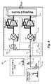
- FIG. 1 illustrates a block diagram of a wireless communication device 100 in which the subject technology may be used in accordance with one or more implementations.
- the wireless communication device 100 includes an antenna 102 , a receiver front end 104 , a baseband processing module 106 , a processor 108 , a memory 110 , and a LO generation module (LOGEN) 112 .
- the blocks represented in FIG. 1 may be integrated on semiconductor substrates.
- the blocks 104 - 112 may be realized in a single system-on-chip, or realized in a multi-chip chipset.
- the antenna 102 is configured to transmit and/or receive wireless signals over a range of frequencies. Although a single antenna is illustrated, the subject disclosure is not so limited.
- the receiver front end 104 includes logic, circuitry and/or interfaces that are configured to receive and process signals from the antenna 102 .
- the receiver front end 104 may be configured to amplify and/or down-covert received wireless signals.
- the receiver front end 104 also may be configured to cancel noise arising from impedance matching and may be linear over a wide range of frequencies.
- the receiver front end 104 may receive signals in accordance with a variety of wireless standards.
- the receiver front end 104 may be applicable to standards, including but not limited to, Wi-Fi, WiMAX, Bluetooth, and various cellular standards. Details regarding the receiver front end 104 are discussed further herein.
- the baseband processing module 106 includes logic, circuitry and/or interfaces that are configured to perform processing of baseband signals.
- the baseband processing module 106 may, for example, analyze received signals and generate control and/or feedback signals for configuring various components of the wireless communication device 100 such as the receiver front end 104 .
- the baseband processing module 106 is configured to encode, decode, transcode, modulate, demodulate, encrypt, decrypt, scramble, descramble, and/or otherwise process data in accordance with wireless standards.
- the baseband processing module 106 may be configured to determine frequency bands associated with desired received signals as well as frequency bands associated with blockers, determine conductance gain coefficients for down-converted spectrum segments that correspond to the desired received signals, and determine calibration coefficients for the one or more digitized spectrum segments based on an amount of interference between the LO harmonics. Details regarding the processes performed by the baseband processing module 106 are discussed further herein.
- the processor 108 includes logic, circuitry and/or interfaces that are configured to process data and/or control operations of the wireless communication device 100 .
- the processor 108 is configured to provide control signals to various other portions of the wireless communication device 100 .
- the processor 108 may control transfers of data between various portions of the wireless communication device 100 .
- the processor 108 may provide for implementation of an operating system or otherwise execute code to manage operations of the wireless communication device 100 .
- the processes performed by the baseband processing module 106 and the processor 108 can be performed by a single processing device, or processes performed by the baseband processing module 106 can also be performed by the processor 108 . Therefore, references to the baseband processing module 106 and the processor 108 throughout the disclosure can be used interchangeably.
- the memory 110 includes logic, circuitry and/or interfaces for storage of various types of information such as received data, generated data, code, and/or configuration information.
- the memory 110 may include a non-transitory storage medium, including but not limited to, RAM, ROM, flash, and/or magnetic storage. According to some implementations of the subject disclosure, information stored in the memory 110 is utilized for configuring the receiver front end 104 and/or the baseband processing module 106 .
- the LOGEN 112 includes logic, circuitry and/or interfaces that are configured to generate oscillating signals at multiple frequencies.
- the LOGEN 112 may be configured to generate digital and/or analog signals.
- the LOGEN 112 is configured to generate clock signals and/or sinusoidal signals. Characteristics of the oscillating signals such as the frequency and duty cycle may be determined based on control signals from the processor 108 and/or the baseband processing module 106 .
- the processor 108 configures the various components of the wireless communication device 100 based on a wireless standard according to which it is desired to receive signals.
- Wireless signals are received via the antenna 102 , amplified and down-converted by the receiver front end 104 .
- the baseband processing module 106 may perform noise estimation and/or noise cancellation, decoding, and/or demodulation of the baseband signals.
- information in the received signal is recovered and utilized appropriately.
- the information may be audio and/or video to be presented to a user of the wireless communication device 100 , data to be stored to the memory 110 , and/or information affecting and/or enabling operation of the wireless communication device 100 .
- FIGS. 2A and 2B illustrate exemplary graphs of local oscillator (LO) signal and gain waveforms for I/Q mixers.
- An ideal mixer multiplies an incoming RF signal with a complex LO sinusoid, which frequency shifts a desired frequency channel to DC.
- an ideal I/Q hard-switched mixer approximates the complex sinusoid by two square waves that are offset by a quarter period, however, this approximation results in aliasing of signals around the 3 rd , 5 th and 7 th harmonics, and so on. Although attenuated relative to the desired frequency, this undesired signal folding may be unacceptable for a true wideband receiver.
- this signal folding also applies to noise, and can limit the noise figure (NF) to 0.9 dB because of antenna noise folding alone.
- the I/Q mixer shown in FIG. 2A can be viewed as a multiplication of the RF signal with a complex sinewave that is sampled-and-held at twice the Nyquist frequency. Therefore, to shift these aliasing terms to higher frequencies, the sampling rate can be increased. For instance, if the LO waveform is sampled-and-held at eight times the receive frequency, the first alias is moved to 7th harmonic and is attenuated by 17 dB relative to the desired signal, as shown in FIG. 2B . Also, increasing the sampling rate also improves conversion loss, and the minimum achievable noise figure also improves to 0.2 dB. In some implementations, the oversampling may come at the cost of an increased burden on LO generation circuitry.
- FIG. 3A is a diagram of a mixer 300 for the RF front end 104 with associated LO clock waveforms
- FIG. 3B illustrates exemplary graphs of LO signal waveforms for the mixer 300
- the oversampling mixer 300 is a passive-mixer-based mixer with eight phases.
- a RF current is first down-converted by mixer switches 302 driven by non-overlapping clocks, sw(t ⁇ x/MT)), x ⁇ [0, . . . , M ⁇ 1].
- the down-converted currents are then scaled to voltages at transinductance amplifiers (TIAs) 304 , appropriately weighted at weighting blocks 306 and summed at summing block 308 .
- the TIA output is given by:
- These constants can be determined by the processor 108 so that the output of the summation block 308 generates a sampled version of an ideal complex sinusoid, which becomes the effective LO that down-converts the incoming RF signal. For example, by setting
- the output around base-band is given by
- g ARB
- e j ⁇ g ARB is an predetermined baseband gain
- ⁇ LO is a clock frequency
- ⁇ is some carrier offset. Therefore, as well as receiving desired signals around ⁇ LO + ⁇ , signals at offsets of integer multiples of M ⁇ LO are also down-converted.
- phase of the clock pulses are modified by changing the baseband weighting constants, which results in an complex periodic waveform being generated with a predetermined amount of phase offset.
- graphs 310 and 312 illustrate a time shift and magnitude change for the output of the summation block 308 that can be achieved by modifying the complex weighting constants for the phases of the mixer 300 .
- the time shift and magnitude modification allows for a correction in phase (and magnitude) variations between two down-conversion paths in a noise-cancelling receiver without employing two separate LO chains. Details regarding the down-conversion paths of the noise-cancelling receiver are discussed further herein.
- FIG. 4 illustrates a mixer-first receiver front end 400 in accordance with embodiments of the present disclosure that utilizes noise canceling techniques.
- the mixer-first receiver front end 400 can be implemented in various devices to receive wireless RF signals, such as cell phones, wireless modems, wireless routers and access points, etc.
- the mixer-first receiver front end 400 can be implemented in the RF front end 104 of the communication device 100 .
- the mixer-first receiver front end 400 includes an antenna 402 , two down-conversion paths 404 and 406 , and a baseband processing block 408 that performs weighting and recombination of the outputs of the two down-conversion paths 404 and 406 .
- the receiver front end 400 also includes a transconductance cell 422 , passive mixers 416 and 420 , and transimpedance amplifiers 424 and 426 .
- the antenna 402 can be represented by a voltage source 410 in series with a source output resistance (RS) 412 , which can be, for example, 50 Ohms.
- RS source output resistance
- the source output resistance 412 can be matched by an input matching resistance in main down-conversion path 404 to avoid signal reflections and maximize power transfer from the antenna 402 to the other down-stream elements of the mixer-first receiver front end 400 .
- the transconductance cell (G M ) 422 is included in the auxiliary down-conversion path 406 to convert an RF signal input (e.g., V R IN ) into a corresponding current signal.
- the transconductance cell 422 can be implemented, for example, as an inverter.
- the transconductance cell 422 includes logic, circuitry and/or interfaces that are configured to output a current that is proportional to a voltage input to the transconductance cell 422 .
- the passive mixers 416 and 420 each include logic and/or circuitry that may provide for generation of inter-modulation products resulting from mixing the RF signal input 205 with LO signals (e.g., LO 0 , LO 1 , . . . , LOM ⁇ 1) generated by the LOGEN 112 ( FIG. 1 ).
- the passive mixers 416 and 420 are metal-oxide semiconductor field effect transistors (MOSFETs).
- the passive mixers 416 and 420 may be n-channel MOSFETs (e.g., NMOS).
- the passive mixers 416 and 420 can be implemented using other switching devices.
- the passive mixers 416 and 420 are configured to operate in their linear region when powered on.
- the transimpedance amplifier (TIA) 426 includes logic, circuitry and/or interfaces that are configured to output a voltage that is proportional to a current input to the TIA 426 .
- the TIA 424 includes logic, circuitry and/or interfaces that are configured to output a voltage that is proportional to a current input to the TIA 424 .
- the two down-conversion paths 404 and 406 down-convert an RF signal received by the antenna 402 to baseband or some IF and to substantially cancel thermal noise generated by the input matching resistance R SW , while substantially avoiding voltage gain of the RF signal.
- the main down-conversion path 404 includes passive mixers 416 to down-convert the current signal I R IN flowing through an input matching resistance by an amount substantially equal to the frequency of a LO signal 418 (e.g., LO 0 -LOM ⁇ 1).
- the current signal I R IN includes both the RF signal received by the antenna 402 and the thermal noise signal generated by the input matching resistance R SW .
- the auxiliary down-conversion path 406 includes a passive mixer 420 to down-convert the voltage signal V R IN measured between the source output resistance 412 and the input matching resistance R SW by an amount substantially equal to the frequency of the same LO signal 418 used by passive mixer 416 .
- the frequency of the LO signal 418 can be tuned, for example, over a wide frequency range based on a position of a desired channel in the spectrum of the received RF signal.
- the voltage signal V R IN includes both the RF signal received by the antenna 402 and the thermal noise signal generated by the input matching resistance R SW .
- the thermal noise signal and the RF signal appear in both the current signal I R IN and the voltage signal V R IN , the thermal noise signal in V R IN is 180 degrees out of phase with the thermal noise signal in I R IN , while the RF signal in V R IN is in-phase with the RF signal in I R IN .
- the TIAs 424 and 426 can be respectively used to convert and scale the down-converted current signals at the output of passive mixers 418 and 420 , into two voltage signals V OUT1 and V OUT2 such that, when V OUT1 and V OUT2 are added together (or potentially sensed differentially depending on the relative polarities of the gains applied by the transfer functions), the thermal noise generated by input matching resistance is substantially canceled, while the RF signal received by antenna 402 is reinforced.
- the voltage signals V OUT1 and V OUT2 define the In-phase (I) and Quadrature (Q) components of the RF signal input.
- the transfer functions of the TIAs 424 and 426 are determined based on their feedback networks.
- the feedback networks for the TIAs 224 and 226 include impedance elements Z MAIN and Z AUX that can have a resistive element and a capacitive element in parallel.
- the capacitive elements of the impedance elements Z MAIN and Z AUX can be included for stability purposes and the resistive elements of the impedance elements Z MAIN and Z AUX can be included to set a current-to-voltage conversion gain for the TIAs 224 and 226 , respectively.
- the magnitude of the two voltage signals V OUT1 and V OUT2 can be adjusted such that, when V OUT1 and V OUT2 are added together (or potentially sensed differentially depending on the relative polarities of ⁇ and r m ), the thermal noise generated by input matching resistance is substantially canceled, while the RF signal received by antenna 402 is reinforced.
- other settings for the resistance elements are possible and can be used for other RF receiver front end configurations.
- a virtual ground at the negative summing nodes of TIAs 424 and 426 appears ideally at the RF side of passive mixers 416 and 420 where the RF signal from the antenna 402 is received, thereby suppressing voltage swing prior to baseband or IF filtering to remove blockers.
- mixer-first receiver front end 400 suppresses noise, while minimizing voltage gain, the mixer-first receiver front end 400 can be considered blocker-tolerant.
- passive mixer 416 is bidirectional, the noise of the TIA 224 is up-converted at the input of the mixer-first receiver front end 400 and is canceled along with the thermal noise generated by input matching resistance in the main down-conversion path 404 .
- the noise of the TIA 226 contributes negligibly when driven by a current source-like transconductance cell 222 .
- baseband processing block 408 processes V OUT1 and V OUT2 using one or more processors and/or circuits.
- the processor 108 and/or baseband processing module 106 of the communication device 100 executes one or more software processes associated with the functionality of the baseband processing block 408 .
- baseband processing block 408 can low-pass filter V OUT1 and V OUT2 , either separately or after having been added (or subtracted) together, to remove blockers and other interference.
- baseband processing block 408 can further perform digitization of V OUT1 and V OUT2 , either separately or after having been added (or subtracted) together, using one or more analog-to-digital converters (ADCs).
- the ADCs can be, for example, delta-sigma ADCs.
- baseband processing block 408 can perform low-pass filtering and digitization of V OUT1 and V OUT2 in any order relative to each other. Further, baseband processing block 408 can demodulate the down-converted RF signal contained within V OUT1 and V OUT2 to recover information.
- the LO signal 418 used by passive mixers 416 and 420 in FIG. 4 to down-convert a received RF signal typically approximates a square waveform. Unlike a single-tone sinusoidal waveform, a square waveform contains harmonics at specific multiples of the fundamental frequency of the LO signal. Consequently, undesired portions of the RF signal located at these harmonics can be down-converted by the passive mixers 416 and 420 and interfere with a desired portion of the RF signal at baseband.
- the mixer-first receiver front end 400 can be designed to limit interference caused by these higher-order harmonic effects.
- the mixers 416 and 420 respectively included in down-conversion paths 404 and 406 can be implemented as a multi-phase passive harmonic rejection mixer.
- the mixers 416 and 420 can be an eight-phase passive harmonic rejection mixer constructed from four single-balanced passive mixers.
- the TIAs 224 and 226 can be implemented by multiple TIAs (e.g., four) that are each coupled to a respective one of the single-balanced passive mixers that correspond to each of the LO phases. It should be noted that, in other embodiments, lower or higher order passive harmonic rejection mixers can be used.
- the single-balanced passive mixers included in each down-conversion path 404 and 406 receive a respective set of LO signals. For example, for an eight-phase LO mixer (with phases 0 through 7 ), a first respective passive mixer in down-conversion paths 404 and 406 receives LO signals 0 and 4 , a second respective passive mixer in down-conversion paths 404 and 406 receives LO signals 1 and 5 , a third respective passive mixer in down-conversion paths 404 and 406 receives LO signals 2 and 6 , and a fourth respective passive mixer in down-conversion paths 404 and 406 receives LO signals 3 and 7 .
- the exemplary LO signals are non-overlapping and have a duty-cycle substantially equal to 12.5%. It can be shown that, by using appropriately weighted combinations of the outputs of the four TIAs in each down-conversion path 404 and 406 , the amount of noise that folds down to baseband as a result of the higher-order harmonic effects discussed above can be reduced and/or nulled.
- the weighting and recombination can be performed by baseband processing block 408 .
- the receiver front end 400 can be further constructed as a fully differential receiver front end.
- the receiver front end 400 can be further constructed to process a differential RF signal received by the antenna 402 by replacing the transconductance cell 422 with a differential transconductance cell and by replacing the passive mixers in each down-conversion path 404 and 406 with differential passive mixers.
- the receiver front end can selectively receive one or more down-converted RF spectrum segments by modifying weighting factors of transconductance cells associated with the TIAs for each of the non-overlapping LO phases.
- the dynamic range and sampling speed of the ADCs can be reduced while still achieving wideband frequency coverage.
- FIG. 5A illustrates an exemplary diagram of a harmonic selective full band capture (FBC) receiver front end 500 .
- the receiver front end 500 includes a multi-phase mixer 502 that is tuned by non-overlapping LO signals 504 that correspond to each of the M phases.
- the mixer 502 is a 32-phase mixer that is tuned by 32 non-overlapping LO signals 504 .
- the receiver front end 500 can also include TIAs 506 at the outputs of each phase of the mixer 502 that can be configured to receive M down-conversion signals from the respective phases of the mixer 502 .
- Each of the TIAs 506 includes one or more transconductance cells with a particular transconductance weighting to output a weighted current signal.
- Outputs of the TIAs 506 are coupled to a common feedback impedance, which is coupled to an input of a respective one of the TIAs 506 to convert the weighted current signal into a voltage output with a voltage gain such that a desired signal associated with one or more selected harmonics realizes the voltage gain and undesired signals corresponding to harmonics at blocker or other undesired signal locations are rejected without amplification.
- Each of the outputs of the multi-phase mixer 502 contains down-converted spectrums corresponding to the ⁇ 1 st to the ⁇ (M/2 ⁇ 1) th harmonics of a fundamental LO frequency.
- the received signals around the k-th harmonic e.g. k*F LO
- one or more harmonics from the ⁇ 1st and ⁇ (M/2 ⁇ 1) th harmonic can be selectively received by weighting coefficients that correspond to spectrum segments associated with each of the harmonics in the received signal spectrum.
- the broadband spectrum is channelized into M/2 narrower spectrum segments or channels and can therefore be sampled by ADCs with a speed that is M times slower than high-speed ADCs that are used in DS receivers.
- baseband processing module 508 controls the weighting coefficients for each of the received spectrum segments for the ⁇ 1 st to the ⁇ (M/2 ⁇ 1) th harmonics of the fundamental LO frequency.
- the spectrum segments associated with the 1 st , 4 th , and 7 th harmonics of the fundamental LO frequency correspond to the desired spectrum segments, and all of the other received spectrum segments are undesired spectrum segments. Therefore, the processing circuitry of the baseband processing module 508 determines the weighting coefficients so that the spectrum segments associated with the 1 st , 4 th , and 7 th harmonics are amplified, and all other spectrum segments are rejected. For example, FIGS.
- FIG. 5B, 6, and 7 illustrate exemplary graphs of LO signals and gain waveforms for the receiver front end 500 .
- the graphs in FIG. 5B correspond to the mixer output for the 1 st harmonic
- the graphs in FIG. 6 correspond to the mixer output for the 4 th harmonic
- the graphs in FIG. 7 correspond to the mixer output for the 7 th harmonic.
- the processing circuitry determines the desired spectrum segments to be amplified based on frequency bands associated with the received signal.
- the frequency bands of the received signal can be determined based on frequency channels associated with a wireless signal protocol of the received signals that can include Long Term Evolution (LTE), Wireless Local Area Network (WLAN), Global System for Mobile Communication (GSM), Global Positioning System (GPS), Blutetooth (BT), or any other type of wireless signal protocol that is known.
- LTE Long Term Evolution
- WLAN Wireless Local Area Network
- GSM Global System for Mobile Communication
- GPS Global Positioning System
- BT Blutetooth
- the processing circuitry can also determine the undesired spectrum segments to be rejected based on frequency locations of blockers or any other type of interference signal.
- the receiver receives a limited number of signals in predetermined frequency bands.
- the baseband processing module 508 can tune the LO frequency according to the frequency of the signals such that after down-conversion, the baseband frequencies of the received signal are reduced or minimized, which can also further reduce a sampling speed of the ADCs.
- the LO frequency can be tuned such that the blockers are attenuated by low pass filters in the baseband paths.
- the baseband processing module 508 can also apply anti-aliasing filter 702 in the RF domain to remove out-of-band blockers at the 25 th and 39 th harmonics while retaining the signal information at the desired 7 th harmonic.
- the filtering of the blockers results in a relaxation of the dynamic range specifications of sampling ADCs. For instance, if two arbitrary LTE/WLAN/GPS/BT signals (800 MHz to 1 GHz, 1.4 GHz to 1.6 GHz, or 1800 GHz to 2500 GHz) are received, the LO frequency is tunable around 150 MHz with 32 phases and 30% tuning range, and blockers may be as close as 80 MHz away from the signals. By tuning the LO frequency, the baseband blocker frequency, F b,out , to signal frequency, F s,out , a harmonic rejection ratio is greater than 2.5 and F s,out is less than 50 MHz.
- the blockers can be attenuated by at least 30 dB, which leads to a reduction by twenty times in the power consumption of the sampling ADCs under Schreier FOM.
- the sampling speed of the ADCs under Nyquist criteria can also be reduced from 300 MHz to 100 MHz.
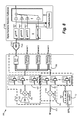
- FIG. 8 illustrates a schematic diagram of a harmonic selective FBC receiver front end 800 .
- a source of interference in the harmonic selective receiver with the receiver front end 800 is that blockers that are present at undesired harmonics associated with down-converted spectrum segments, which can be down-converted within the pass-band at the baseband.
- the receiver front end 800 implements noise-cancelling techniques and harmonic rejection TIAs while amplifying one or more desired spectrum segments that correspond to a received signal spectrum and rejecting one or more undesired spectrum segments that correspond to blocker frequencies.
- the mixer-first receiver front end 800 can be implemented in various devices to receive wireless RF signals, such as cell phones, wireless modems, wireless routers and access points, etc.
- the mixer-first receiver front end 800 can be implemented in the RF front end 104 of the communication device 100 .
- the receiver front end 800 has some structural elements that are similar to the receiver front end 400 ; however, the receiver front end 800 provides the ability to amplify the desired spectrum segments while rejecting the undesired spectrum segments.
- the receiver front end 800 also has similar structural elements to the receiver front end 500 but also includes two down-conversion paths 804 and 806 to provide improved noise cancelling along with a digital calibration block 840 to reduce the effects of phase and amplitude mismatches that may occur in the LO down-conversion.
- the receiver front end 800 is a mixer-first receiver front end that includes two down-conversion paths 804 and 806 , and a baseband processing block 808 that performs weighting and recombination of the outputs of the two down-conversion paths 804 and 806 that results in amplification of one or more desired spectrum segments.
- the receiver front end 800 also includes a transconductance cell 822 , multi-phase mixers 816 and 820 , and transimpedance amplifiers 824 and 826 .
- the transconductance cell (G M ) 822 is included in the auxiliary down-conversion path 806 to convert an RF signal input (e.g., V R IN ) into a corresponding current signal.
- the transconductance cell 822 can be implemented, for example, as an inverter.
- the transconductance cell 822 includes logic, circuitry and/or interfaces that are configured to output a current that is proportional to a voltage input to the transconductance cell 822 .
- the passive mixers 816 and 820 each include logic and/or circuitry that may provide for generation of inter-modulation products resulting from mixing the RF signal input 805 with LO signals 818 (e.g., LO 0 , LO 1 , . . . , LOM ⁇ 1) generated by the LOGEN 112 ( FIG. 1 ).
- the mixers 816 and 420 are metal-oxide semiconductor field effect transistors (MOSFETs).
- the passive mixers 816 and 820 may be n-channel MOSFETs (e.g., NMOS).
- the passive mixers 816 and 820 can be implemented using other switching devices.
- the passive mixers 816 and 820 are configured to operate in their linear region when powered on.
- the receiver front end 800 includes the mixers 816 and 820 in both down-conversion paths 804 and 806 , which are multi-phase mixers that are tuned by non-overlapping LO signals 818 that correspond to each of the M phases.
- the mixers 816 and 820 are 32-phase mixers that are tuned by 32 non-overlapping LO signals 504 .
- the down-conversion paths 804 and 806 also include TIAs 824 and 826 at the outputs of each phase of the mixers 816 and 820 that can be configured to receive M down-conversion signals from the respective phases of the mixers 816 and 820 .
- Each of the TIAs 824 and 826 includes one or more transconductance cells with a particular transconductance weighting to output a weighted current signal. Outputs of the TIAs 824 and 826 are coupled to a common feedback impedance, which is coupled to an input of a respective one of the TIAs 824 and 826 to convert the weighted current signal into a voltage output with a voltage gain such that a desired signal associated with one or more selected harmonics realizes the voltage gain and undesired signals corresponding to harmonics at blocker or other undesired signal locations are rejected without amplification.
- the TIAs 824 and 826 are referred to as harmonic selective TIAs.
- baseband processing module 808 determines and controls the weighting coefficients for each of the received spectrum segments for the ⁇ 1 st to the ⁇ (M/2 ⁇ 1) th harmonics of the fundamental LO frequency. In one implementation, the baseband processing module 808 determines the weighting coefficients for the spectrum segments associated with the three harmonics (e.g., Channel 1 , Channel 2 , Channel 3 ) of the fundamental LO frequency that correspond to the desired spectrum segments, and all of the other received spectrum segments are undesired spectrum segments.
- the baseband processing module 808 determines and controls the weighting coefficients for each of the received spectrum segments for the ⁇ 1 st to the ⁇ (M/2 ⁇ 1) th harmonics of the fundamental LO frequency. In one implementation, the baseband processing module 808 determines the weighting coefficients for the spectrum segments associated with the three harmonics (e.g., Channel 1 , Channel 2 , Channel 3 ) of the fundamental LO frequency that correspond to the desired spectrum segments, and all of the other received spectrum segments are undesired spectrum segments
- the effective transconductance value (G m,EFF ) for the TIAs 824 in the main down-conversion path 804 is large for the desired harmonics and zero for the undesired harmonics. Therefore, only desired harmonics are amplified by the TIAs 824 .
- a DC offset is introduced to the transconductance (G M ) units for the TIAs to maintain positive values for the transconductance (G M ) weighting coefficients, which may result in the 0 th harmonic not being rejected as well as increased power consumption.
- the 0 th harmonic can be rejected if desired with filtering by DC block capacitors at the RF input 805 .
- the increased power consumption may result in higher noise from the transconductance (G M ) stages of the TIAs.
- the amount of DC offset applied to maintain positive values for the transconductance (G M ) weighting coefficients decreases, which reduces the power consumption.
- no harmonic rejection is performed and the harmonic selective TIAs 824 becomes single-input single-output TIAs.
- the main down-conversion path 804 may not saturated by harmonic blockers.
- the transconductance (G M ) weighting coefficients for the harmonic selective TIAs 826 vary slightly from the transconductance (G M ) weighting coefficients for the main down-conversion path 804 . If the values for the transconductance (G M ) weighting coefficients in the main down-conversion path 804 are adopted for the TIAs 826 in the auxiliary down-conversion path 806 , an input impedance seen by the undesired harmonic blockers can be large, which can result in large voltage swings at the output of the transconductance cell 822 and the input of the TIAs 826 .
- an effective G M value is determined for the undesired harmonics, G m,EFF,off , that is less than the effective G M value for the desired harmonics G m,EFF,on , such that the voltage gain across the transconductance cell 822 is less than 10 dB. If k d,i and k u,i are sets of desired and undesired harmonics for the TIAs 826 , respectively, then the G M values for the TIAs 826 in the auxiliary down-conversion path 806 can be described by:
- ⁇ aux G m , EFF , on ⁇ ⁇ i ⁇ ⁇ cos ⁇ 2 ⁇ ⁇ ⁇ ⁇ k d , i ⁇ n M + G m , EFF , off ⁇ ⁇ i ⁇ ⁇ cos ⁇ 2 ⁇ ⁇ ⁇ ⁇ k u , i ⁇ n M ( Eq . ⁇ 5 )
- G M value for the undesired harmonics, G m,EFF,off increases from zero, the voltage gain at the output of the TIAs 826 increases, thus trading off a reduced gain at the output of the transconductance cell 822 .
- G m , EFF , off G m , EFF , on 5 , such that voltage gains at for both the main down-conversion path 804 and the auxiliary down-conversion path 806 are less than 10 dB so that a ⁇ 10 dBm harmonic blocker can be tolerated.
- the analog output of the baseband processing block 808 is digitized by M ADCs 842 with a sampling rate F ADC , where M corresponds to the number of non-overlapping phases of the LO.
- M corresponds to the number of non-overlapping phases of the LO.
- a harmonic rejection ratio at the analog baseband outputs may be limited to 40 ⁇ 50 dB. Therefore, although the harmonic blockers may not saturate the receiver, the received signal can still become corrupted if the blockers fall on top of the desired signals after down-conversion is performed.
- the harmonic rejection ratio can be further improved by performing a digital calibration at digital calibration block 840 .
- the digital calibration block 840 includes logic, circuitry and/or interfaces that are configured to receive and process signals, and the functions associated with the digital calibration block 840 may be executed as software processes by processing circuitry of the processor 108 .
- a signal-to-noise ratio (SNR) specification for the M ADCs 842 can be relaxed by M times, resulting in a reduction in total power consumption.
- SNR signal-to-noise ratio
- the mismatch information from the LO can be retained and digitally corrected at the digital calibration block 840 by applying amplitude corrections on each of the M outputs, so that the undesired harmonics between the ⁇ (M/2 ⁇ 1) th and (M/2 ⁇ 1) th can be fully rejected.
- the ⁇ (M/2 ⁇ 1) th to the (M/2 ⁇ 1) th harmonic includes all of the harmonics within a captured spectrum, e.g. the Nyquist bandwidth in an equivalent DS system.
- Higher order harmonics can be filtered in the RF domain because the higher order harmonics also cause aliasing issues and are outside the capturing range.
- the filtering of the higher order harmonics in the RF domain can be performed by the filter 702 ( FIG. 7 ).
- calibration coefficients, ⁇ ij can be determined at the digital calibration block 840 by injecting a single test tone at the i th harmonic, monitoring the output power at the i th and j th harmonic outputs, P(i,j) and P(i,i). Any phase and/or amplitude mismatches during the LO down-conversion may result in signal leakage between the received LO harmonics. The signal leakage may be caused by signals from the desired spectrum segments or the undesired spectrum segments.
- the 4 th harmonic of the received signal may correspond to a blocker signal frequency, which is rejected based on the transconductance values (GM) applied to the TIAs 824 and 826 , but may still cause signal leakage into other desired spectrum segments associated with other harmonics.
- the digital calibration block 840 can measure the amount of signal leakage from the 4 th harmonic into other received harmonics.
- the output power can be measured at the harmonics other than the 4 th harmonic caused by the test tone inserted at the 4 th harmonic and compared to the output power at the 4 th harmonic, and the calibration coefficient, ⁇ 4j , can be calculated for each of the other harmonics.
- the digital calibration block 808 can then apply the calibration coefficient to the harmonics of the received signal to remove the effects of any phase and/or amplitude mismatches that may have occurred during the LO down-conversion.
- the calibration coefficient for the test tone inserted i th harmonic can be described by the following equation:
- the receiver front end 800 can be implemented on a test chip that is fabricated in 28 nm CMOS, and the core area of the harmonic selective FBC receiver is 3 mm 2 .
- the LO is in 32-phase, thus 16 harmonics can be received with I/Q outputs, and the fundamental LO frequency is tunable from 127.5 MHz to 172.5 MHz.
- the 32 TIA outputs are digitized by external low-speed ADCs (ADAS1126).
- harmonic recombination blocks can also implemented on the chip.
- FIG. 9 is an exemplary diagram of a harmonic selective FBC receiver front end 900 .
- the structure and function of the receiver front end 900 is substantially similar to the receiver front end 500 described previously.
- the receiver front end 900 includes a multi-phase mixer 902 that is tuned by non-overlapping LO signals 904 that correspond to each of the M phases.
- the mixer 902 is a 64-phase mixer that is tuned by 64 non-overlapping LO signals 904 .
- the receiver front end 900 can also include TIAs 906 at the outputs of each phase of the mixer 902 that can be configured to receive M down-conversion signals from the respective phases of the mixer 902 .
- Each of the TIAs 906 includes one or more transconductance cells with a particular transconductance weighting to output a weighted current signal. Outputs of the TIAs 906 are coupled to a common feedback impedance, which is coupled to an input of a respective one of the TIAs 906 to convert the weighted current signal into a voltage output with a voltage gain such that a desired signal associated with one or more selected harmonics realizes the voltage gain and undesired signals corresponding to harmonics at blocker or other undesired signal locations are rejected without amplification.
- baseband processing module 908 controls the weighting coefficients for each of the received spectrum segments for the ⁇ 1 st to the ⁇ (M/2 ⁇ 1) th harmonics of the fundamental LO frequency.
- the baseband processing module 908 can determine the weighting coefficients for up to thirty-one 50 MHz I/Q channels (e.g., spectrum segments).
- FIG. 10 illustrates exemplary graphs of gain and noise figure for a harmonic selective FBC receiver that includes the receiver front end 900 where the desired spectrum segments correspond to the 3 rd (300 MHz) and 9 th (900 MHz) LO harmonics output from the multi-phase mixer 902 with a LO fundamental frequency of 100 Mhz.
- the gain at the 3 rd and 9 th harmonics is greater than the gain for the other harmonics in the received spectrum, which can be achieved by determining and applying the transconductance G M weighting coefficients as described previously herein for the receiver front end 500 and the receiver front end 800 .
- the noise figure associated with the 3 rd and 9 th harmonics is less than for the other harmonics, which indicates that the 3 rd and 9 th harmonics have greater sensitivity than the other harmonics in the received spectrum.
- FIG. 11A shows a measured small signal gain and noise figure for reception of 4 th (800 MHz) and 9 th harmonics (1800 MHz) as desired spectrum segments based on a LO fundamental frequency of 200 MHz.
- the 10 th harmonic (2000 MHz) is an undesired harmonic so the gain for the 10 th harmonic is much lower than for the 4 th and 9 th harmonics (e.g., 35-45 dB rejection).
- the noise figure is 2-4 dB depending on the received harmonics, as higher harmonics have worse noise aliasing from their images.
- a worst case 80 MHz blocker occurs when the signal frequencies are 2100 MHz and 2190 MHz, while the blocker is at 2270 MHz.
- the LO frequency is tuned to 153.5 MHz to achieve a greatest amount of attenuation of the blocker, and both signals are down-converted from the 14th harmonic.
- the blocker resides at 121 MHz, while the output bandwidth is 49 MHz in order to pass both signals.
- the gain and noise figure versus blocker power is plotted in FIG. 11B .
- the blocker is also down-converted to 32.5 MHz at the 15th harmonic of the LO, which is within the baseband output bandwidth. The measurement result shows that the receiver could tolerate both large blockers that are close to baseband as well as harmonic blockers.
- the harmonic rejection calibration can also be applied, which results in an improvement in the harmonic rejection ratio from 50 dB to >80 dB for all the harmonics within the capturing range.
- the calibration results reduces the effects of random or systematic mismatches in the 32-phase LO, mixers, baseband TIAs, and the sampling ADCs.
- Table 1 provides a comparison between the harmonic selective FBC receiver described herein and other DS and wideband receivers. Compared to existing solutions, the harmonic selective FBC receiver architecture achieves superior sensitivity and dynamic range, uses narrower LO tuning range to cover the wide bandwidth, and leads to significant power savings for wireless FBC applications.
- FIG. 12 is an exemplary flowchart of a process 1200 for selecting and processing one or more spectrum segments of a harmonic selective FBC receiver.
- the process 1200 is described with respect to the receiver front end 800 , but it can be understood that one or more steps of the process 1200 can be applied to harmonic selective FBC receivers having structures that differ from the receiver front end 800 .
- the non-overlapping LO signals 818 for the multi-phase mixers 816 and 820 are tuned so that the baseband frequencies of the desired received signal are less than a predetermined threshold.
- the LO signals 818 can also be tuned so that a baseband blocker frequency corresponds to a low-pass filter frequency, such as a frequency within a filtering band of an anti-aliasing filter.
- the receiver receives a limited number of signals in predetermined frequency bands so the baseband processing module 508 can tune the LO frequencies according to the frequency of the signals such that after down-conversion, the baseband frequencies of the received signal are reduced or minimized, which can also further reduce a sampling speed of the ADCs.
- the LO frequency can be tuned such that the blockers are attenuated by low-pass filters in the baseband paths.
- the processing circuitry of the baseband processing block 808 determines the desired and undesired spectrum segments based on frequency bands associated with the received signal and blockers.
- the processing circuitry determines the desired spectrum segments to be amplified based on frequency bands associated with the received signal.
- the frequency bands of the received signal can be determined based on frequency channels associated with a wireless signal protocol of the received signals that can include LTE, WLAN, GSM, GPS, BT, or any other type of wireless signal protocol that is known.
- the processing circuitry can also determine the undesired spectrum segments to be rejected based on frequency locations of blockers or any other type of interference signal.
- a received signal is down-converted into one or more spectrum segments at the multi-phase mixers 816 and 820 in the main and auxiliary down-conversion paths 804 and 806 of the receiver front end 800 .
- Each of the outputs of the multi-phase mixer 816 and 820 contains down-converted spectrums corresponding to the ⁇ 1 st to the ⁇ (M/2 ⁇ 1) th harmonics of the fundamental LO frequency.
- the received signals around the k-th harmonic e.g. k*F LO , have a phase shift of 2 ⁇ kn/M.
- transconductance (GM) weighting coefficients are applied to the desired and undesired spectrum segments so that the desired spectrum segments are amplified and the undesired spectrum segments are rejected.
- the baseband processing module 808 determines and controls the weighting coefficients for each of the received spectrum segments for the ⁇ 1 st to the ⁇ (M/2 ⁇ 1) th harmonics of the fundamental LO frequency.
- the effective transconductance value (G m,EFF ) for the TIAs 824 in the main down-conversion path 804 is large for the desired harmonics and zero for the undesired harmonics. Therefore, only desired harmonics are amplified by the TIAs 824 .
- a DC offset is introduced to the transconductance (G M ) units for the TIAs to maintain positive values for the transconductance (G M ) weighting coefficients, which may result in the 0 th harmonic not being rejected as well as increased power consumption.
- the 0 th harmonic can be rejected if desired with filtering by DC block capacitors at the RF input 805 .
- the increased power consumption may result in higher noise from the transconductance (G M ) stages of the TIAs.
- the amount of DC offset applied to maintain positive values for the transconductance (G M ) weighting coefficients decreases, which reduces the power consumption.
- no harmonic rejection is performed and the harmonic selective TIAs 824 becomes single-input single-output TIAs.
- the main down-conversion path 804 may not saturated by harmonic blockers.
- the transconductance (G M ) weighting coefficients for the harmonic selective TIAs 826 vary slightly from the transconductance (G M ) weighting coefficients for the main down-conversion path 804 . If the values for the transconductance (G M ) weighting coefficients in the main down-conversion path 804 are adopted for the TIAs 826 in the auxiliary down-conversion path 806 , an input impedance seen by the undesired harmonic blockers can be large, which can result in large voltage swings at the output of the transconductance cell 822 and the input of the TIAs 826 .
- an effective G M value is determined for the undesired harmonics, G m,EFF,off , that is less than the effective G M value for the desired harmonics G m,EFF,on , such that the voltage gain across the transconductance cell 822 is less than 10 dB. If k d,i and k u,i are sets of desired and undesired harmonics for the TIAs 826 , respectively, then the G M values for the TIAs 826 in the auxiliary down-conversion path 806 can be described by Eq. 5.
- a digital calibration process is performed on a digitized output of the baseband processing block 808 to reduce the effects of signal leakage between spectrum segments due to phase and/or amplitude mismatches that may occur during LO down-conversion. Due to the phase and amplitude mismatches in the LO signals 818 , a harmonic rejection ratio at the analog baseband outputs may be limited to 40 ⁇ 50 dB. Therefore, although the harmonic blockers may not saturate the receiver, the received signal can still become corrupted if the blockers fall on top of the desired signals after down-conversion is performed. In one example, the harmonic rejection ratio can be further improved by performing the digital calibration process at digital calibration block 840 . Details regarding the digital calibration process are discussed further herein.
- FIG. 13 is an exemplary flowchart of a process 1300 for performing calibration of a harmonic selective FBC receiver.
- the process 1300 is an implementation of the digital calibration process that is performed at step S 1210 of the process 1200 .
- a test tone is inserted at a harmonic that correspond to one of the down-converted spectrum segments.
- the 4 th harmonic of the received signal may correspond to a blocker signal frequency, which is rejected based on the transconductance values (GM) applied to the TIAs 824 and 826 , but may still cause signal leakage into other desired spectrum segments associated with other harmonics.
- the digital calibration block 840 can insert the test tone at the 4 th harmonic in order to determine how much of the signal content at the 4 th harmonic leaks into the other harmonics of the received signal spectrum.
- the amount of interference at other harmonics of the down-converted signal spectrum due to the inserted test tone is measured. If the test tone is inserted at the i th harmonic, then the output power is measured at the i th and j th harmonic outputs, (i,) and (i,).
- the j th harmonic outputs can correspond to the power outputs at each harmonic other than the i th harmonic where the test tone is inserted. For example, if the test tone is inserted at the 4 th harmonic, then the output power is measured at the harmonics other than the 4 th harmonic caused by the test tone inserted at the 4 th harmonic and compared to the output power at the 4 th harmonic.
- the calibration coefficient is for the test tone inserted i th harmonic, which is described by Eq. 5.
- steps S 1302 , S 1304 , and S 1306 of the process 1300 are performed for each down-converted harmonic in the received signal spectrum so that the effects of signal leakage from each of the spectrum segments into the other down-converted spectrum segments can be measured and removed by the determined calibration coefficients.
- the calculated calibration coefficients are applied to the digitalized signal by the digital calibration block 840 effects of signal leakage between spectrum segments due to phase and/or amplitude mismatches that may occur during LO down-conversion.
Landscapes
- Engineering & Computer Science (AREA)
- Computer Networks & Wireless Communication (AREA)
- Signal Processing (AREA)
- Power Engineering (AREA)
- Noise Elimination (AREA)
Abstract
Description
which corresponds to the RF current multiplied by a summation of the product of the complex weighting constants, [K0, . . . , KM-1], and their associated clock waveforms, as shown in
an oversampled complex LO with a predetermined magnitude of |gARB| down-converts the RF signal. In the frequency domain, the output around base-band is given by
where gARB=|gARB|ej∠g
such that voltage gains at for both the main down-
| TABLE 1 | |||
| Direct | Wideband | Harmonic Selective | |
| Topology | Sampling FBC | SDR | |
| CMOS Technology | |||
| 28 nm | 65 |
28 nm | |
| Capturing Band | 0-2500 | 0-3200 | 700-2500 |
| [MHz] | |||
| Number of |
8 | 8 | 32 |
| NF [dB] | 30 (w/o extra | 3 | 2~4 |
| LNA) | |||
| Blocker Dynamic | 86.1 | 95.8 | 95.8 |
| Range [dB] | |||
| |
0% | 200% | 30% |
| HR Ratio [dB] | 54.7 | 52 | >80 (with calibration) |
| Power [mW] | 150 | 36 | 25 |
| Active Area | 0.45 | 5.0 | 3.0 |
Claims (19)
Priority Applications (1)
| Application Number | Priority Date | Filing Date | Title |
|---|---|---|---|
| US15/240,344 US10027358B2 (en) | 2016-08-15 | 2016-08-18 | Harmonic selective full-band capture receiver with digital harmonic rejection calibration |
Applications Claiming Priority (2)
| Application Number | Priority Date | Filing Date | Title |
|---|---|---|---|
| US201662375188P | 2016-08-15 | 2016-08-15 | |
| US15/240,344 US10027358B2 (en) | 2016-08-15 | 2016-08-18 | Harmonic selective full-band capture receiver with digital harmonic rejection calibration |
Publications (2)
| Publication Number | Publication Date |
|---|---|
| US20180048339A1 US20180048339A1 (en) | 2018-02-15 |
| US10027358B2 true US10027358B2 (en) | 2018-07-17 |
Family
ID=61159467
Family Applications (1)
| Application Number | Title | Priority Date | Filing Date |
|---|---|---|---|
| US15/240,344 Active 2036-08-31 US10027358B2 (en) | 2016-08-15 | 2016-08-18 | Harmonic selective full-band capture receiver with digital harmonic rejection calibration |
Country Status (1)
| Country | Link |
|---|---|
| US (1) | US10027358B2 (en) |
Cited By (6)
| Publication number | Priority date | Publication date | Assignee | Title |
|---|---|---|---|---|
| US11240070B1 (en) * | 2020-10-30 | 2022-02-01 | Feature Integration Technology Inc. | Digital isolator |
| US11356136B2 (en) * | 2020-09-08 | 2022-06-07 | Shenzhen GOODIX Technology Co., Ltd. | Harmonic rejection in multiphase signals |
| US11431379B1 (en) * | 2021-03-31 | 2022-08-30 | Teradyne, Inc. | Front-end module |
| US20220286151A1 (en) * | 2021-03-05 | 2022-09-08 | Motorola Solutions, Inc. | Linearizing narrowband carriers with low resolution predistorters |
| US20230039029A1 (en) * | 2020-08-28 | 2023-02-09 | Rockwell Automation Technologies, Inc. | Safety Rated Input Module for an Industrial Controller |
| US11750427B1 (en) * | 2022-05-04 | 2023-09-05 | L3Harris Technologies, Inc. | Low-noise highly-linear wideband vector modulators |
Families Citing this family (18)
| Publication number | Priority date | Publication date | Assignee | Title |
|---|---|---|---|---|
| US10027358B2 (en) * | 2016-08-15 | 2018-07-17 | Avago Technologies General Ip (Singapore) Pte. Ltd. | Harmonic selective full-band capture receiver with digital harmonic rejection calibration |
| EP3336561A1 (en) * | 2016-12-13 | 2018-06-20 | Nxp B.V. | Method and apparatus for generating a frequency estimation signal |
| US10142137B2 (en) | 2017-03-02 | 2018-11-27 | Micron Technology, Inc. | Wireless devices and systems including examples of full duplex transmission |
| US11941516B2 (en) | 2017-08-31 | 2024-03-26 | Micron Technology, Inc. | Cooperative learning neural networks and systems |
| US10554375B2 (en) | 2017-09-11 | 2020-02-04 | Micron Technology, Inc. | Full duplex device-to-device cooperative communication |
| US11206050B2 (en) * | 2018-02-06 | 2021-12-21 | Micron Technology, Inc. | Self interference noise cancellation to support multiple frequency bands |
| CN110299951B (en) * | 2018-03-23 | 2022-04-22 | 中兴通讯股份有限公司 | Phase calibration method and device |
| US10432242B1 (en) * | 2018-05-09 | 2019-10-01 | Morse Micro Pty Ltd | Low noise broadband amplifier with resistive matching |
| US10523182B1 (en) | 2018-08-22 | 2019-12-31 | Rockwell Collins, Inc. | Adaptive harmonic cancellation |
| US10778188B1 (en) * | 2019-02-22 | 2020-09-15 | Qualcomm Incorporated | Harmonic rejection filter with transimpedence amplifiers |
| US10938428B2 (en) | 2019-02-25 | 2021-03-02 | Huawei Technologies Co., Ltd. | Wireless receiver system for neutralizing blocking signals |
| CN110731054B (en) * | 2019-04-29 | 2020-10-09 | Oppo广东移动通信有限公司 | Method and apparatus for controlling harmonic interference |
| US10979097B2 (en) | 2019-09-05 | 2021-04-13 | Micron Technology, Inc. | Wireless devices and systems including examples of full duplex transmission using neural networks or recurrent neural networks |
| US11177988B2 (en) * | 2020-01-23 | 2021-11-16 | Shenzhen GOODIX Technology Co., Ltd. | Receiver circuits with blocker attenuating mixer |
| US11258473B2 (en) | 2020-04-14 | 2022-02-22 | Micron Technology, Inc. | Self interference noise cancellation to support multiple frequency bands with neural networks or recurrent neural networks |
| US20210105031A1 (en) * | 2020-12-17 | 2021-04-08 | Amichay Israel | Mitigating receiver oscillator leakage between coexisting wireless technologies |
| GB202101010D0 (en) * | 2021-01-26 | 2021-03-10 | Nordic Semiconductor Asa | Multiband radio receivers |
| CN116184043B (en) * | 2023-03-15 | 2023-08-29 | 北京航空航天大学 | Broadband electromagnetic environment monitoring system for unmanned aerial vehicle platform |
Citations (22)
| Publication number | Priority date | Publication date | Assignee | Title |
|---|---|---|---|---|
| US20050239430A1 (en) * | 2004-03-12 | 2005-10-27 | Rf Magic, Inc. | Harmonic suppression mixer and tuner |
| US7139544B2 (en) * | 2003-09-22 | 2006-11-21 | Intel Corporation | Direct down-conversion receiver with transconductance-capacitor filter and method |
| US20060293017A1 (en) * | 2003-04-28 | 2006-12-28 | Young-Jin Kim | Circuit and method for receiving and mixing radio frequencies in a direct conversion receiver |
| US20080284487A1 (en) * | 2005-09-06 | 2008-11-20 | Rajasekhar Pullela | Passive Mixer And High Q RF Filter Using A Passive Mixer |
| US20090143031A1 (en) * | 2005-03-11 | 2009-06-04 | Peter Shah | Harmonic suppression mixer and tuner |
| US7570936B2 (en) * | 2006-10-27 | 2009-08-04 | Avago Technologies Wireless Ip (Singapore) Pte. Ltd. | Sub-harmonically pumped mixer |
| US20100019848A1 (en) * | 2008-07-28 | 2010-01-28 | Paolo Rossi | Complementary Low Noise Transductor with Active Single Ended to Differential Signal Conversion |
| US20110222633A1 (en) * | 2010-01-05 | 2011-09-15 | Maxlinear, Inc. | High dynamic range radio architecture with enhanced image rejection |
| US8081937B2 (en) * | 2007-11-29 | 2011-12-20 | Broadcom Corporation | Gain-control methods of transmitter modulators |
| US20130169378A1 (en) * | 2011-12-30 | 2013-07-04 | Avago Technologies Wireless Ip (Singapore) Pte. Ltd. | Apparatus having double phase-matched configuration for reducing magnitude of intermodulation products |
| US20140112418A1 (en) * | 2012-10-22 | 2014-04-24 | Gct Semiconductor, Inc. | Receiver using impedance shaping |
| US8761710B2 (en) * | 2010-06-03 | 2014-06-24 | Broadcom Corporation | Portable computing device with a saw-less transceiver |
| US20150063509A1 (en) * | 2013-08-30 | 2015-03-05 | Qualcomm Incorporated | Blocker filtering for noise-cancelling receiver |
| US9014653B2 (en) * | 2012-09-16 | 2015-04-21 | Technische Universiteit Delft | High-IF superheterodyne receiver incorporating high-Q complex band pass filter |
| US9088471B1 (en) * | 2014-02-19 | 2015-07-21 | Qualcomm Incorporated | Quadrature combining and adjusting |
| US9124335B1 (en) * | 2012-12-13 | 2015-09-01 | Broadcom Corporation | Wideband receiver robust to radio frequency harmonics |
| US20150304155A1 (en) * | 2014-04-16 | 2015-10-22 | University Of Macau | ZigBee Receiver Exploiting an RF-to-BB Current-Reuse Blixer and Hybrid Filter Topology |
| US9219507B2 (en) * | 2012-08-13 | 2015-12-22 | Broadcom Corporation | Blocker-tolerant wideband noise-canceling receivers |
| US20160142085A1 (en) * | 2014-11-14 | 2016-05-19 | Qualcomm Incorporated | Sawless architecture for receivers |
| US9595985B1 (en) * | 2015-10-01 | 2017-03-14 | Broadcom Corporation | Power reduction in noise-cancelling receivers |
| US9729119B1 (en) * | 2016-03-04 | 2017-08-08 | Atmel Corporation | Automatic gain control for received signal strength indication |
| US20180048339A1 (en) * | 2016-08-15 | 2018-02-15 | Broadcom Corporation | Harmonic selective full-band capture receiver with digital harmonic rejection calibration |
-
2016
- 2016-08-18 US US15/240,344 patent/US10027358B2/en active Active
Patent Citations (27)
| Publication number | Priority date | Publication date | Assignee | Title |
|---|---|---|---|---|
| US20060293017A1 (en) * | 2003-04-28 | 2006-12-28 | Young-Jin Kim | Circuit and method for receiving and mixing radio frequencies in a direct conversion receiver |
| US7139544B2 (en) * | 2003-09-22 | 2006-11-21 | Intel Corporation | Direct down-conversion receiver with transconductance-capacitor filter and method |
| US20050239430A1 (en) * | 2004-03-12 | 2005-10-27 | Rf Magic, Inc. | Harmonic suppression mixer and tuner |
| US20090143031A1 (en) * | 2005-03-11 | 2009-06-04 | Peter Shah | Harmonic suppression mixer and tuner |
| US20080284487A1 (en) * | 2005-09-06 | 2008-11-20 | Rajasekhar Pullela | Passive Mixer And High Q RF Filter Using A Passive Mixer |
| US7570936B2 (en) * | 2006-10-27 | 2009-08-04 | Avago Technologies Wireless Ip (Singapore) Pte. Ltd. | Sub-harmonically pumped mixer |
| US8275332B2 (en) * | 2007-11-29 | 2012-09-25 | Broadcom Corporation | Gain-control methods of transmitter modulators |
| US8081937B2 (en) * | 2007-11-29 | 2011-12-20 | Broadcom Corporation | Gain-control methods of transmitter modulators |
| US20120071119A1 (en) * | 2007-11-29 | 2012-03-22 | Broadcom Corporation | Gain-control methods of transmitter modulators |
| US20100019848A1 (en) * | 2008-07-28 | 2010-01-28 | Paolo Rossi | Complementary Low Noise Transductor with Active Single Ended to Differential Signal Conversion |
| US20110222633A1 (en) * | 2010-01-05 | 2011-09-15 | Maxlinear, Inc. | High dynamic range radio architecture with enhanced image rejection |
| US8798216B2 (en) * | 2010-01-05 | 2014-08-05 | Maxlinear, Inc. | High dynamic range radio architecture with enhanced image rejection |
| US9246719B2 (en) * | 2010-01-05 | 2016-01-26 | Maxliner, Inc. | High dynamic range radio architecture with enhanced image rejection |
| US8761710B2 (en) * | 2010-06-03 | 2014-06-24 | Broadcom Corporation | Portable computing device with a saw-less transceiver |
| US20130169378A1 (en) * | 2011-12-30 | 2013-07-04 | Avago Technologies Wireless Ip (Singapore) Pte. Ltd. | Apparatus having double phase-matched configuration for reducing magnitude of intermodulation products |
| US9083311B2 (en) * | 2011-12-30 | 2015-07-14 | Avago Technologies General Ip (Singapore) Pte. Ltd. | Apparatus having double phase-matched configuration for reducing magnitude of intermodulation products |
| US9219507B2 (en) * | 2012-08-13 | 2015-12-22 | Broadcom Corporation | Blocker-tolerant wideband noise-canceling receivers |
| US9014653B2 (en) * | 2012-09-16 | 2015-04-21 | Technische Universiteit Delft | High-IF superheterodyne receiver incorporating high-Q complex band pass filter |
| US20140112418A1 (en) * | 2012-10-22 | 2014-04-24 | Gct Semiconductor, Inc. | Receiver using impedance shaping |
| US9124335B1 (en) * | 2012-12-13 | 2015-09-01 | Broadcom Corporation | Wideband receiver robust to radio frequency harmonics |
| US20150063509A1 (en) * | 2013-08-30 | 2015-03-05 | Qualcomm Incorporated | Blocker filtering for noise-cancelling receiver |
| US9088471B1 (en) * | 2014-02-19 | 2015-07-21 | Qualcomm Incorporated | Quadrature combining and adjusting |
| US20150304155A1 (en) * | 2014-04-16 | 2015-10-22 | University Of Macau | ZigBee Receiver Exploiting an RF-to-BB Current-Reuse Blixer and Hybrid Filter Topology |
| US20160142085A1 (en) * | 2014-11-14 | 2016-05-19 | Qualcomm Incorporated | Sawless architecture for receivers |
| US9595985B1 (en) * | 2015-10-01 | 2017-03-14 | Broadcom Corporation | Power reduction in noise-cancelling receivers |
| US9729119B1 (en) * | 2016-03-04 | 2017-08-08 | Atmel Corporation | Automatic gain control for received signal strength indication |
| US20180048339A1 (en) * | 2016-08-15 | 2018-02-15 | Broadcom Corporation | Harmonic selective full-band capture receiver with digital harmonic rejection calibration |
Non-Patent Citations (3)
| Title |
|---|
| David Murphy, et al., "A Blocker-Tolerant, Noise-Cancelling Receiver Suitable for Wideband Wireless Applications", IEEE Journal of Solid-State Circuits, vol. 47, No. 12, Dec. 2012, pp. 2943-2963. |
| David Murphy, et al., "A Noise-Cancelling Receiver with Enhanced Resilience to Harmonic Blockers", IEEE International Solid-State Circuits Conference, ISSCC, Digest of Technical Papers, Session 3, Feb. 10, 2014, pp. 68-70. |
| Jiangfeng Wu, et al., "A 2.7 mW/Channel 48/1000 MHz Direct Sampling Full-Band Cable Receiver", IEEE Journal of Solid-State Circuits, vol. 51, No. 4, Apr. 2016, pp. 845-859. |
Cited By (8)
| Publication number | Priority date | Publication date | Assignee | Title |
|---|---|---|---|---|
| US20230039029A1 (en) * | 2020-08-28 | 2023-02-09 | Rockwell Automation Technologies, Inc. | Safety Rated Input Module for an Industrial Controller |
| US11716178B2 (en) * | 2020-08-28 | 2023-08-01 | Rockwell Automation Technologies, Inc. | Safety rated input module for an industrial controller |
| US11356136B2 (en) * | 2020-09-08 | 2022-06-07 | Shenzhen GOODIX Technology Co., Ltd. | Harmonic rejection in multiphase signals |
| US11240070B1 (en) * | 2020-10-30 | 2022-02-01 | Feature Integration Technology Inc. | Digital isolator |
| US20220286151A1 (en) * | 2021-03-05 | 2022-09-08 | Motorola Solutions, Inc. | Linearizing narrowband carriers with low resolution predistorters |
| US11456760B1 (en) * | 2021-03-05 | 2022-09-27 | Motorola Solutions, Inc. | Linearizing narrowband carriers with low resolution predistorters |
| US11431379B1 (en) * | 2021-03-31 | 2022-08-30 | Teradyne, Inc. | Front-end module |
| US11750427B1 (en) * | 2022-05-04 | 2023-09-05 | L3Harris Technologies, Inc. | Low-noise highly-linear wideband vector modulators |
Also Published As
| Publication number | Publication date |
|---|---|
| US20180048339A1 (en) | 2018-02-15 |
Similar Documents
| Publication | Publication Date | Title |
|---|---|---|
| US10027358B2 (en) | Harmonic selective full-band capture receiver with digital harmonic rejection calibration | |
| US9219507B2 (en) | Blocker-tolerant wideband noise-canceling receivers | |
| US9124335B1 (en) | Wideband receiver robust to radio frequency harmonics | |
| US10014894B2 (en) | Down-conversion circuit | |
| US8520786B2 (en) | Programmable discrete digital receiver components | |
| US9325360B2 (en) | Reducing non-linearities in a differential receiver path prior to a mixer using calibration | |
| US8670739B1 (en) | Frequency-translational bandpass filter with harmonic rejection | |
| Wu et al. | A harmonic-selective multi-band wireless receiver with digital harmonic rejection calibration | |
| US10111280B2 (en) | Multi-carrier base station receiver | |
| US9037106B2 (en) | Baseband harmonic rejection circuit | |
| US9525447B1 (en) | Radio receiver co-existence | |
| Tripathi et al. | Characterization of hardware impairments in software defined radio | |
| Mailand et al. | Compensation of DC-offsets and RF-self-mixing products in six-port-based analog direct receivers | |
| Gao et al. | Transceiver II: Receiver Architectures |
Legal Events
| Date | Code | Title | Description |
|---|---|---|---|
| AS | Assignment |
Owner name: BROADCOM CORPORATION, CALIFORNIA Free format text: ASSIGNMENT OF ASSIGNORS INTEREST;ASSIGNORS:WU, HAO;MURPHY, DAVID PATRICK;DARABI, HOOMAN;REEL/FRAME:039476/0057 Effective date: 20160817 |
|
| AS | Assignment |
Owner name: AVAGO TECHNOLOGIES GENERAL IP (SINGAPORE) PTE. LTD., SINGAPORE Free format text: ASSIGNMENT OF ASSIGNORS INTEREST;ASSIGNOR:BROADCOM CORPORATION;REEL/FRAME:041706/0001 Effective date: 20170120 Owner name: AVAGO TECHNOLOGIES GENERAL IP (SINGAPORE) PTE. LTD Free format text: ASSIGNMENT OF ASSIGNORS INTEREST;ASSIGNOR:BROADCOM CORPORATION;REEL/FRAME:041706/0001 Effective date: 20170120 |
|
| STCF | Information on status: patent grant |
Free format text: PATENTED CASE |
|
| AS | Assignment |
Owner name: AVAGO TECHNOLOGIES INTERNATIONAL SALES PTE. LIMITE Free format text: MERGER;ASSIGNOR:AVAGO TECHNOLOGIES GENERAL IP (SINGAPORE) PTE. LTD.;REEL/FRAME:047422/0464 Effective date: 20180509 |
|
| AS | Assignment |
Owner name: AVAGO TECHNOLOGIES INTERNATIONAL SALES PTE. LIMITE Free format text: CORRECTIVE ASSIGNMENT TO CORRECT THE EXECUTION DATE PREVIOUSLY RECORDED AT REEL: 047422 FRAME: 0464. ASSIGNOR(S) HEREBY CONFIRMS THE MERGER;ASSIGNOR:AVAGO TECHNOLOGIES GENERAL IP (SINGAPORE) PTE. LTD.;REEL/FRAME:048883/0702 Effective date: 20180905 |
|
| MAFP | Maintenance fee payment |
Free format text: PAYMENT OF MAINTENANCE FEE, 4TH YEAR, LARGE ENTITY (ORIGINAL EVENT CODE: M1551); ENTITY STATUS OF PATENT OWNER: LARGE ENTITY Year of fee payment: 4 |