TWI733246B - Electro-optic displays - Google Patents
Electro-optic displays Download PDFInfo
- Publication number
- TWI733246B TWI733246B TW108140715A TW108140715A TWI733246B TW I733246 B TWI733246 B TW I733246B TW 108140715 A TW108140715 A TW 108140715A TW 108140715 A TW108140715 A TW 108140715A TW I733246 B TWI733246 B TW I733246B
- Authority
- TW
- Taiwan
- Prior art keywords
- display
- electro
- pixel
- optical
- display pixels
- Prior art date
Links
Images


Classifications
-
- G—PHYSICS
- G09—EDUCATION; CRYPTOGRAPHY; DISPLAY; ADVERTISING; SEALS
- G09G—ARRANGEMENTS OR CIRCUITS FOR CONTROL OF INDICATING DEVICES USING STATIC MEANS TO PRESENT VARIABLE INFORMATION
- G09G3/00—Control arrangements or circuits, of interest only in connection with visual indicators other than cathode-ray tubes
- G09G3/20—Control arrangements or circuits, of interest only in connection with visual indicators other than cathode-ray tubes for presentation of an assembly of a number of characters, e.g. a page, by composing the assembly by combination of individual elements arranged in a matrix no fixed position being assigned to or needed to be assigned to the individual characters or partial characters
- G09G3/34—Control arrangements or circuits, of interest only in connection with visual indicators other than cathode-ray tubes for presentation of an assembly of a number of characters, e.g. a page, by composing the assembly by combination of individual elements arranged in a matrix no fixed position being assigned to or needed to be assigned to the individual characters or partial characters by control of light from an independent source
- G09G3/3433—Control arrangements or circuits, of interest only in connection with visual indicators other than cathode-ray tubes for presentation of an assembly of a number of characters, e.g. a page, by composing the assembly by combination of individual elements arranged in a matrix no fixed position being assigned to or needed to be assigned to the individual characters or partial characters by control of light from an independent source using light modulating elements actuated by an electric field and being other than liquid crystal devices and electrochromic devices
- G09G3/344—Control arrangements or circuits, of interest only in connection with visual indicators other than cathode-ray tubes for presentation of an assembly of a number of characters, e.g. a page, by composing the assembly by combination of individual elements arranged in a matrix no fixed position being assigned to or needed to be assigned to the individual characters or partial characters by control of light from an independent source using light modulating elements actuated by an electric field and being other than liquid crystal devices and electrochromic devices based on particles moving in a fluid or in a gas, e.g. electrophoretic devices
-
- G—PHYSICS
- G02—OPTICS
- G02F—OPTICAL DEVICES OR ARRANGEMENTS FOR THE CONTROL OF LIGHT BY MODIFICATION OF THE OPTICAL PROPERTIES OF THE MEDIA OF THE ELEMENTS INVOLVED THEREIN; NON-LINEAR OPTICS; FREQUENCY-CHANGING OF LIGHT; OPTICAL LOGIC ELEMENTS; OPTICAL ANALOGUE/DIGITAL CONVERTERS
- G02F1/00—Devices or arrangements for the control of the intensity, colour, phase, polarisation or direction of light arriving from an independent light source, e.g. switching, gating or modulating; Non-linear optics
- G02F1/01—Devices or arrangements for the control of the intensity, colour, phase, polarisation or direction of light arriving from an independent light source, e.g. switching, gating or modulating; Non-linear optics for the control of the intensity, phase, polarisation or colour
- G02F1/165—Devices or arrangements for the control of the intensity, colour, phase, polarisation or direction of light arriving from an independent light source, e.g. switching, gating or modulating; Non-linear optics for the control of the intensity, phase, polarisation or colour based on translational movement of particles in a fluid under the influence of an applied field
- G02F1/1675—Constructional details
- G02F1/1676—Electrodes
-
- G—PHYSICS
- G09—EDUCATION; CRYPTOGRAPHY; DISPLAY; ADVERTISING; SEALS
- G09G—ARRANGEMENTS OR CIRCUITS FOR CONTROL OF INDICATING DEVICES USING STATIC MEANS TO PRESENT VARIABLE INFORMATION
- G09G3/00—Control arrangements or circuits, of interest only in connection with visual indicators other than cathode-ray tubes
- G09G3/20—Control arrangements or circuits, of interest only in connection with visual indicators other than cathode-ray tubes for presentation of an assembly of a number of characters, e.g. a page, by composing the assembly by combination of individual elements arranged in a matrix no fixed position being assigned to or needed to be assigned to the individual characters or partial characters
- G09G3/34—Control arrangements or circuits, of interest only in connection with visual indicators other than cathode-ray tubes for presentation of an assembly of a number of characters, e.g. a page, by composing the assembly by combination of individual elements arranged in a matrix no fixed position being assigned to or needed to be assigned to the individual characters or partial characters by control of light from an independent source
- G09G3/3433—Control arrangements or circuits, of interest only in connection with visual indicators other than cathode-ray tubes for presentation of an assembly of a number of characters, e.g. a page, by composing the assembly by combination of individual elements arranged in a matrix no fixed position being assigned to or needed to be assigned to the individual characters or partial characters by control of light from an independent source using light modulating elements actuated by an electric field and being other than liquid crystal devices and electrochromic devices
- G09G3/344—Control arrangements or circuits, of interest only in connection with visual indicators other than cathode-ray tubes for presentation of an assembly of a number of characters, e.g. a page, by composing the assembly by combination of individual elements arranged in a matrix no fixed position being assigned to or needed to be assigned to the individual characters or partial characters by control of light from an independent source using light modulating elements actuated by an electric field and being other than liquid crystal devices and electrochromic devices based on particles moving in a fluid or in a gas, e.g. electrophoretic devices
- G09G3/3446—Control arrangements or circuits, of interest only in connection with visual indicators other than cathode-ray tubes for presentation of an assembly of a number of characters, e.g. a page, by composing the assembly by combination of individual elements arranged in a matrix no fixed position being assigned to or needed to be assigned to the individual characters or partial characters by control of light from an independent source using light modulating elements actuated by an electric field and being other than liquid crystal devices and electrochromic devices based on particles moving in a fluid or in a gas, e.g. electrophoretic devices with more than two electrodes controlling the modulating element
-
- G—PHYSICS
- G02—OPTICS
- G02F—OPTICAL DEVICES OR ARRANGEMENTS FOR THE CONTROL OF LIGHT BY MODIFICATION OF THE OPTICAL PROPERTIES OF THE MEDIA OF THE ELEMENTS INVOLVED THEREIN; NON-LINEAR OPTICS; FREQUENCY-CHANGING OF LIGHT; OPTICAL LOGIC ELEMENTS; OPTICAL ANALOGUE/DIGITAL CONVERTERS
- G02F1/00—Devices or arrangements for the control of the intensity, colour, phase, polarisation or direction of light arriving from an independent light source, e.g. switching, gating or modulating; Non-linear optics
- G02F1/01—Devices or arrangements for the control of the intensity, colour, phase, polarisation or direction of light arriving from an independent light source, e.g. switching, gating or modulating; Non-linear optics for the control of the intensity, phase, polarisation or colour
- G02F1/13—Devices or arrangements for the control of the intensity, colour, phase, polarisation or direction of light arriving from an independent light source, e.g. switching, gating or modulating; Non-linear optics for the control of the intensity, phase, polarisation or colour based on liquid crystals, e.g. single liquid crystal display cells
- G02F1/133—Constructional arrangements; Operation of liquid crystal cells; Circuit arrangements
- G02F1/136—Liquid crystal cells structurally associated with a semi-conducting layer or substrate, e.g. cells forming part of an integrated circuit
- G02F1/1362—Active matrix addressed cells
- G02F1/136213—Storage capacitors associated with the pixel electrode
-
- G—PHYSICS
- G02—OPTICS
- G02F—OPTICAL DEVICES OR ARRANGEMENTS FOR THE CONTROL OF LIGHT BY MODIFICATION OF THE OPTICAL PROPERTIES OF THE MEDIA OF THE ELEMENTS INVOLVED THEREIN; NON-LINEAR OPTICS; FREQUENCY-CHANGING OF LIGHT; OPTICAL LOGIC ELEMENTS; OPTICAL ANALOGUE/DIGITAL CONVERTERS
- G02F1/00—Devices or arrangements for the control of the intensity, colour, phase, polarisation or direction of light arriving from an independent light source, e.g. switching, gating or modulating; Non-linear optics
- G02F1/01—Devices or arrangements for the control of the intensity, colour, phase, polarisation or direction of light arriving from an independent light source, e.g. switching, gating or modulating; Non-linear optics for the control of the intensity, phase, polarisation or colour
- G02F1/13—Devices or arrangements for the control of the intensity, colour, phase, polarisation or direction of light arriving from an independent light source, e.g. switching, gating or modulating; Non-linear optics for the control of the intensity, phase, polarisation or colour based on liquid crystals, e.g. single liquid crystal display cells
- G02F1/133—Constructional arrangements; Operation of liquid crystal cells; Circuit arrangements
- G02F1/136—Liquid crystal cells structurally associated with a semi-conducting layer or substrate, e.g. cells forming part of an integrated circuit
- G02F1/1362—Active matrix addressed cells
- G02F1/136286—Wiring, e.g. gate line, drain line
-
- G—PHYSICS
- G02—OPTICS
- G02F—OPTICAL DEVICES OR ARRANGEMENTS FOR THE CONTROL OF LIGHT BY MODIFICATION OF THE OPTICAL PROPERTIES OF THE MEDIA OF THE ELEMENTS INVOLVED THEREIN; NON-LINEAR OPTICS; FREQUENCY-CHANGING OF LIGHT; OPTICAL LOGIC ELEMENTS; OPTICAL ANALOGUE/DIGITAL CONVERTERS
- G02F1/00—Devices or arrangements for the control of the intensity, colour, phase, polarisation or direction of light arriving from an independent light source, e.g. switching, gating or modulating; Non-linear optics
- G02F1/01—Devices or arrangements for the control of the intensity, colour, phase, polarisation or direction of light arriving from an independent light source, e.g. switching, gating or modulating; Non-linear optics for the control of the intensity, phase, polarisation or colour
- G02F1/15—Devices or arrangements for the control of the intensity, colour, phase, polarisation or direction of light arriving from an independent light source, e.g. switching, gating or modulating; Non-linear optics for the control of the intensity, phase, polarisation or colour based on an electrochromic effect
-
- G—PHYSICS
- G02—OPTICS
- G02F—OPTICAL DEVICES OR ARRANGEMENTS FOR THE CONTROL OF LIGHT BY MODIFICATION OF THE OPTICAL PROPERTIES OF THE MEDIA OF THE ELEMENTS INVOLVED THEREIN; NON-LINEAR OPTICS; FREQUENCY-CHANGING OF LIGHT; OPTICAL LOGIC ELEMENTS; OPTICAL ANALOGUE/DIGITAL CONVERTERS
- G02F1/00—Devices or arrangements for the control of the intensity, colour, phase, polarisation or direction of light arriving from an independent light source, e.g. switching, gating or modulating; Non-linear optics
- G02F1/01—Devices or arrangements for the control of the intensity, colour, phase, polarisation or direction of light arriving from an independent light source, e.g. switching, gating or modulating; Non-linear optics for the control of the intensity, phase, polarisation or colour
- G02F1/165—Devices or arrangements for the control of the intensity, colour, phase, polarisation or direction of light arriving from an independent light source, e.g. switching, gating or modulating; Non-linear optics for the control of the intensity, phase, polarisation or colour based on translational movement of particles in a fluid under the influence of an applied field
- G02F1/166—Devices or arrangements for the control of the intensity, colour, phase, polarisation or direction of light arriving from an independent light source, e.g. switching, gating or modulating; Non-linear optics for the control of the intensity, phase, polarisation or colour based on translational movement of particles in a fluid under the influence of an applied field characterised by the electro-optical or magneto-optical effect
- G02F1/167—Devices or arrangements for the control of the intensity, colour, phase, polarisation or direction of light arriving from an independent light source, e.g. switching, gating or modulating; Non-linear optics for the control of the intensity, phase, polarisation or colour based on translational movement of particles in a fluid under the influence of an applied field characterised by the electro-optical or magneto-optical effect by electrophoresis
-
- G—PHYSICS
- G02—OPTICS
- G02F—OPTICAL DEVICES OR ARRANGEMENTS FOR THE CONTROL OF LIGHT BY MODIFICATION OF THE OPTICAL PROPERTIES OF THE MEDIA OF THE ELEMENTS INVOLVED THEREIN; NON-LINEAR OPTICS; FREQUENCY-CHANGING OF LIGHT; OPTICAL LOGIC ELEMENTS; OPTICAL ANALOGUE/DIGITAL CONVERTERS
- G02F1/00—Devices or arrangements for the control of the intensity, colour, phase, polarisation or direction of light arriving from an independent light source, e.g. switching, gating or modulating; Non-linear optics
- G02F1/01—Devices or arrangements for the control of the intensity, colour, phase, polarisation or direction of light arriving from an independent light source, e.g. switching, gating or modulating; Non-linear optics for the control of the intensity, phase, polarisation or colour
- G02F1/165—Devices or arrangements for the control of the intensity, colour, phase, polarisation or direction of light arriving from an independent light source, e.g. switching, gating or modulating; Non-linear optics for the control of the intensity, phase, polarisation or colour based on translational movement of particles in a fluid under the influence of an applied field
- G02F1/1675—Constructional details
- G02F1/16757—Microcapsules
-
- G—PHYSICS
- G02—OPTICS
- G02F—OPTICAL DEVICES OR ARRANGEMENTS FOR THE CONTROL OF LIGHT BY MODIFICATION OF THE OPTICAL PROPERTIES OF THE MEDIA OF THE ELEMENTS INVOLVED THEREIN; NON-LINEAR OPTICS; FREQUENCY-CHANGING OF LIGHT; OPTICAL LOGIC ELEMENTS; OPTICAL ANALOGUE/DIGITAL CONVERTERS
- G02F1/00—Devices or arrangements for the control of the intensity, colour, phase, polarisation or direction of light arriving from an independent light source, e.g. switching, gating or modulating; Non-linear optics
- G02F1/01—Devices or arrangements for the control of the intensity, colour, phase, polarisation or direction of light arriving from an independent light source, e.g. switching, gating or modulating; Non-linear optics for the control of the intensity, phase, polarisation or colour
- G02F1/165—Devices or arrangements for the control of the intensity, colour, phase, polarisation or direction of light arriving from an independent light source, e.g. switching, gating or modulating; Non-linear optics for the control of the intensity, phase, polarisation or colour based on translational movement of particles in a fluid under the influence of an applied field
- G02F1/1675—Constructional details
- G02F1/1676—Electrodes
- G02F1/16766—Electrodes for active matrices
-
- G—PHYSICS
- G02—OPTICS
- G02F—OPTICAL DEVICES OR ARRANGEMENTS FOR THE CONTROL OF LIGHT BY MODIFICATION OF THE OPTICAL PROPERTIES OF THE MEDIA OF THE ELEMENTS INVOLVED THEREIN; NON-LINEAR OPTICS; FREQUENCY-CHANGING OF LIGHT; OPTICAL LOGIC ELEMENTS; OPTICAL ANALOGUE/DIGITAL CONVERTERS
- G02F1/00—Devices or arrangements for the control of the intensity, colour, phase, polarisation or direction of light arriving from an independent light source, e.g. switching, gating or modulating; Non-linear optics
- G02F1/01—Devices or arrangements for the control of the intensity, colour, phase, polarisation or direction of light arriving from an independent light source, e.g. switching, gating or modulating; Non-linear optics for the control of the intensity, phase, polarisation or colour
- G02F1/165—Devices or arrangements for the control of the intensity, colour, phase, polarisation or direction of light arriving from an independent light source, e.g. switching, gating or modulating; Non-linear optics for the control of the intensity, phase, polarisation or colour based on translational movement of particles in a fluid under the influence of an applied field
- G02F1/1685—Operation of cells; Circuit arrangements affecting the entire cell
-
- G—PHYSICS
- G09—EDUCATION; CRYPTOGRAPHY; DISPLAY; ADVERTISING; SEALS
- G09G—ARRANGEMENTS OR CIRCUITS FOR CONTROL OF INDICATING DEVICES USING STATIC MEANS TO PRESENT VARIABLE INFORMATION
- G09G3/00—Control arrangements or circuits, of interest only in connection with visual indicators other than cathode-ray tubes
- G09G3/20—Control arrangements or circuits, of interest only in connection with visual indicators other than cathode-ray tubes for presentation of an assembly of a number of characters, e.g. a page, by composing the assembly by combination of individual elements arranged in a matrix no fixed position being assigned to or needed to be assigned to the individual characters or partial characters
- G09G3/2003—Display of colours
-
- G—PHYSICS
- G09—EDUCATION; CRYPTOGRAPHY; DISPLAY; ADVERTISING; SEALS
- G09G—ARRANGEMENTS OR CIRCUITS FOR CONTROL OF INDICATING DEVICES USING STATIC MEANS TO PRESENT VARIABLE INFORMATION
- G09G3/00—Control arrangements or circuits, of interest only in connection with visual indicators other than cathode-ray tubes
- G09G3/20—Control arrangements or circuits, of interest only in connection with visual indicators other than cathode-ray tubes for presentation of an assembly of a number of characters, e.g. a page, by composing the assembly by combination of individual elements arranged in a matrix no fixed position being assigned to or needed to be assigned to the individual characters or partial characters
- G09G3/2007—Display of intermediate tones
-
- G—PHYSICS
- G02—OPTICS
- G02F—OPTICAL DEVICES OR ARRANGEMENTS FOR THE CONTROL OF LIGHT BY MODIFICATION OF THE OPTICAL PROPERTIES OF THE MEDIA OF THE ELEMENTS INVOLVED THEREIN; NON-LINEAR OPTICS; FREQUENCY-CHANGING OF LIGHT; OPTICAL LOGIC ELEMENTS; OPTICAL ANALOGUE/DIGITAL CONVERTERS
- G02F2201/00—Constructional arrangements not provided for in groups G02F1/00 - G02F7/00
- G02F2201/12—Constructional arrangements not provided for in groups G02F1/00 - G02F7/00 electrode
- G02F2201/123—Constructional arrangements not provided for in groups G02F1/00 - G02F7/00 electrode pixel
-
- G—PHYSICS
- G09—EDUCATION; CRYPTOGRAPHY; DISPLAY; ADVERTISING; SEALS
- G09G—ARRANGEMENTS OR CIRCUITS FOR CONTROL OF INDICATING DEVICES USING STATIC MEANS TO PRESENT VARIABLE INFORMATION
- G09G2300/00—Aspects of the constitution of display devices
- G09G2300/04—Structural and physical details of display devices
- G09G2300/0421—Structural details of the set of electrodes
- G09G2300/0426—Layout of electrodes and connections
-
- G—PHYSICS
- G09—EDUCATION; CRYPTOGRAPHY; DISPLAY; ADVERTISING; SEALS
- G09G—ARRANGEMENTS OR CIRCUITS FOR CONTROL OF INDICATING DEVICES USING STATIC MEANS TO PRESENT VARIABLE INFORMATION
- G09G2300/00—Aspects of the constitution of display devices
- G09G2300/08—Active matrix structure, i.e. with use of active elements, inclusive of non-linear two terminal elements, in the pixels together with light emitting or modulating elements
-
- G—PHYSICS
- G09—EDUCATION; CRYPTOGRAPHY; DISPLAY; ADVERTISING; SEALS
- G09G—ARRANGEMENTS OR CIRCUITS FOR CONTROL OF INDICATING DEVICES USING STATIC MEANS TO PRESENT VARIABLE INFORMATION
- G09G2320/00—Control of display operating conditions
- G09G2320/02—Improving the quality of display appearance
- G09G2320/0209—Crosstalk reduction, i.e. to reduce direct or indirect influences of signals directed to a certain pixel of the displayed image on other pixels of said image, inclusive of influences affecting pixels in different frames or fields or sub-images which constitute a same image, e.g. left and right images of a stereoscopic display
-
- G—PHYSICS
- G09—EDUCATION; CRYPTOGRAPHY; DISPLAY; ADVERTISING; SEALS
- G09G—ARRANGEMENTS OR CIRCUITS FOR CONTROL OF INDICATING DEVICES USING STATIC MEANS TO PRESENT VARIABLE INFORMATION
- G09G2320/00—Control of display operating conditions
- G09G2320/02—Improving the quality of display appearance
- G09G2320/0219—Reducing feedthrough effects in active matrix panels, i.e. voltage changes on the scan electrode influencing the pixel voltage due to capacitive coupling
-
- G—PHYSICS
- G09—EDUCATION; CRYPTOGRAPHY; DISPLAY; ADVERTISING; SEALS
- G09G—ARRANGEMENTS OR CIRCUITS FOR CONTROL OF INDICATING DEVICES USING STATIC MEANS TO PRESENT VARIABLE INFORMATION
- G09G2320/00—Control of display operating conditions
- G09G2320/02—Improving the quality of display appearance
- G09G2320/0223—Compensation for problems related to R-C delay and attenuation in electrodes of matrix panels, e.g. in gate electrodes or on-substrate video signal electrodes
Landscapes
- Physics & Mathematics (AREA)
- Nonlinear Science (AREA)
- General Physics & Mathematics (AREA)
- Engineering & Computer Science (AREA)
- Optics & Photonics (AREA)
- Chemical & Material Sciences (AREA)
- Theoretical Computer Science (AREA)
- Computer Hardware Design (AREA)
- Microelectronics & Electronic Packaging (AREA)
- Mathematical Physics (AREA)
- Crystallography & Structural Chemistry (AREA)
- Molecular Biology (AREA)
- Electrochemistry (AREA)
- Health & Medical Sciences (AREA)
- Chemical Kinetics & Catalysis (AREA)
- Life Sciences & Earth Sciences (AREA)
- Power Engineering (AREA)
- Control Of Indicators Other Than Cathode Ray Tubes (AREA)
- Electrochromic Elements, Electrophoresis, Or Variable Reflection Or Absorption Elements (AREA)
Abstract
Description
本申請案係關於2018年11月9日提出之美國臨時申請案62/757,818且主張對其之優先權。This application is related to the U.S. Provisional Application 62/757,818 filed on November 9, 2018 and its priority is claimed.
前述申請案之全文以參照方式併入本文。The full text of the aforementioned application is incorporated herein by reference.
本發明係關於電光顯示器設備,尤其是包含薄膜電晶體陣列之顯示器背板。The present invention relates to electro-optical display devices, especially display backplanes containing thin film transistor arrays.
粒子系之電泳顯示器已成為密集研發主題多年。在此類顯示器中,複數個帶電粒子(有時稱之為顏料粒子)在電場影響下移動經過流體。電場一般係由導電膜或電晶體如場效電晶體提供。相較於液晶顯示器,電泳顯示器具有高亮度及對比度、廣視角、雙穩態及低功耗。但此類電泳顯示器較LCD顯示器之切換速度慢,且電泳顯示器一般在顯示即時視頻時過慢。此外,電泳顯示器在低溫下會因流體黏度限制了電泳粒子移動而遲緩。雖有這些缺點,電泳顯示器見於日常產品如電子書(電子閱讀器)、行動電話及行動電話蓋、智慧卡、標誌、錶、貨架標籤及快閃驅動器。Particle-based electrophoretic displays have been the subject of intensive research and development for many years. In this type of display, a plurality of charged particles (sometimes called pigment particles) move through the fluid under the influence of an electric field. The electric field is generally provided by a conductive film or a transistor such as a field-effect transistor. Compared with liquid crystal displays, electrophoretic displays have high brightness and contrast, wide viewing angles, bi-stable state and low power consumption. However, the switching speed of this type of electrophoretic display is slower than that of the LCD display, and the electrophoretic display is generally too slow when displaying real-time video. In addition, the electrophoretic display is slow at low temperatures due to the fluid viscosity restricting the movement of electrophoretic particles. Despite these shortcomings, electrophoretic displays are found in everyday products such as e-books (e-readers), mobile phones and mobile phone covers, smart cards, signs, watches, shelf labels and flash drives.
許多市售電泳介質基本上僅顯示兩種顏色,以介於黑與白色極端間之漸變,已知為「灰階」。此電泳介質使用具第一顏色之單一類型電泳粒子於具第二不同顏色之有色流體中(在此情況下,當粒子鄰近顯示器觀看表面時顯示第一種顏色,及當粒子遠離顯示器觀看表面時顯示第二種顏色),或是具第一與第二顏色之第一與第二型電泳粒子於無色流體中。在後者情況下,當第一類粒子鄰近顯示器觀看表面時顯示第一種顏色,及當第二類粒子鄰近顯示器觀看表面時顯示第二種顏色。一般這兩種顏色係黑與白。Many commercially available electrophoretic media basically display only two colors, with a gradient between the extremes of black and white, known as "gray scale." This electrophoretic medium uses a single type of electrophoretic particles with a first color in a colored fluid with a second different color (in this case, the first color is displayed when the particles are adjacent to the viewing surface of the display, and when the particles are far away from the viewing surface of the display Display the second color), or first and second type electrophoretic particles with first and second colors in a colorless fluid. In the latter case, the first type of particles display the first color when they are adjacent to the display viewing surface, and the second type of particles display the second color when they are adjacent to the display viewing surface. Generally these two colors are black and white.
雖然看似簡單,電泳介質及電泳裝置顯示複雜行為。例如已發現單純的「導通/關閉」電壓脈衝不足以在電子閱讀器中達成高品質文字。反之,需要以複雜「波形」驅動狀態間之粒子,並確保新顯示的文字未保留先前文字記憶,亦即「鬼影」。Although seemingly simple, electrophoresis media and electrophoresis devices show complex behavior. For example, it has been found that a simple "on/off" voltage pulse is not enough to achieve high-quality text in an e-reader. On the contrary, it is necessary to drive the particles between states with complex "waveforms" and ensure that the newly displayed text does not retain the memory of the previous text, that is, "ghosting".
本發明提供一種電光顯示器,其具有間隔之第一與第二裝置層及顯示像素的一第一與第二列,每一列包括:複數個顯示像素,每一顯示像素具有位於該第一裝置層上用於驅動該顯示像素之一像素電極;位於該第二裝置層上且與該複數個顯示像素之一部分之像素電極重疊之一傳導線;及至少一個傳導路徑,其連接該第一列之傳導線至該等顯示像素的第二列之一傳導線。The present invention provides an electro-optical display, which has spaced first and second device layers and a first and second row of display pixels. Each row includes a plurality of display pixels, and each display pixel has a first device layer located on the first device layer. A pixel electrode on the display pixel; a conductive line located on the second device layer and overlapping with the pixel electrode of a part of the plurality of display pixels; and at least one conductive path connected to the first row The conductive line is connected to a conductive line of the second row of the display pixels.
如前述,此處呈現之主題提供用以降低電容耦合且改善電光顯示器性能之方法及手段。As mentioned above, the subject presented here provides methods and means to reduce capacitive coupling and improve the performance of electro-optical displays.
術語「電光」適用於材料或顯示器,此處採用其在成像技術中的習知意義,係指具有至少一光學性質相異之第一與第二顯示狀態之材料,藉由施加電場至該材料使其自第一顯示狀態變為第二顯示狀態。雖然一般人眼可見的光學性質是顏色,但亦可係其他光學性質如光學穿透性、反射率、照度,或是對於供機器讀取之顯示器而言,在可見光範圍外之電磁波長之 反射率變化意義上的假色(pseudo-color)。The term "electro-optics" is applicable to materials or displays, and its conventional meaning in imaging technology is used here, which refers to materials with at least one first and second display state with different optical properties, by applying an electric field to the material Make it change from the first display state to the second display state. Although the optical property visible to the human eye is color, it can also be other optical properties such as optical penetration, reflectance, illuminance, or reflectance of electromagnetic wavelengths outside the visible range for machine-readable displays Pseudo-color in the sense of change.
術語「灰階狀態」在此處採用其在成像技術中的習知意義,係指介於像素之兩極端光學狀態間的狀態,且非必意指兩極端狀態間之黑白過渡。例如,以下參考之數個E Ink專利與公開申請案中所述電泳顯示器之極端狀態係白與深藍,故中間的「灰階狀態」實際係指淡藍。如前述,光學狀態變化確實可非顏色變化。術語「黑」與「白」在此後可用以指稱顯示器之兩極端光學狀態,且應被視於一般包含非僅黑與白之極端光學狀態,例如前述的白與深藍狀態。術語「單色」在此後可指稱僅將像素驅動至無中間灰階狀態之兩極端光學狀態之驅動機制。The term "gray-scale state" is used here in its conventional meaning in imaging technology, and refers to the state between the two extreme optical states of the pixel, and does not necessarily mean the black and white transition between the two extreme states. For example, the extreme states of the electrophoretic displays described in several E Ink patents and published applications referred to below are white and dark blue, so the "gray state" in the middle actually refers to light blue. As mentioned above, the change of optical state can indeed be non-color change. The terms "black" and "white" can hereinafter be used to refer to the two extreme optical states of the display, and should be regarded as the extreme optical states that generally include not only black and white, such as the aforementioned white and deep blue states. The term "monochrome" can hereinafter refer to a driving mechanism that only drives the pixel to the two extreme optical states without intermediate gray scales.
術語「雙穩的」及「雙穩態」在此處採用其在此技術中的習知意義,係指顯示器包括具有至少一光學性質相異之第一與第二顯示狀態之顯示單元(display elements),且使得在以有限期程定址脈衝驅動任何給定單元後,假定其處於第一或第二顯示狀態,在終止定址脈衝後,該狀態將持續至少數倍(例如至少4倍)於改變顯示單元狀態所需定址脈衝最低期程。在美國專利申請案號2002/0180687(亦參照對應的國際專利申請案公開號WO 02/079869)中顯示有些具灰階之粒子系之電泳顯示器,不僅在極端黑白狀態下穩定,在其中間的灰階狀態亦然,且此對於一些其他類型的電光顯示器亦同。此類顯示器適合稱之為「多穩態」而非雙穩態,然為便利之故,術語「雙穩態」在此可用以涵蓋雙穩態及多穩態顯示器。The terms "bistable" and "bistable" are used here in their conventional meanings in this technology, and mean that the display includes a display unit having at least one first and second display state with different optical properties (display elements), so that after driving any given unit with a finite-period addressing pulse, it is assumed to be in the first or second display state. After the addressing pulse is terminated, the state will last at least several times (for example, at least 4 times). The minimum duration of the address pulse required to change the state of the display unit. In the US Patent Application No. 2002/0180687 (also refer to the corresponding International Patent Application Publication No. WO 02/079869), it shows that some electrophoretic displays with gray-scale particle systems are not only stable under extreme black and white conditions, but also in the middle The same is true for the gray-scale state, and this is also true for some other types of electro-optical displays. This type of display is suitable to be called "multi-stable" rather than bistable. However, for convenience, the term "bistable" can be used here to cover both bistable and multi-stable displays.
術語「突波(impulse)」在此處採用其習知意義,係指電壓對時間之積分。但有些雙穩態電光介質充作電荷傳感器,且具此介質可採用突波之一替代定義,亦即電流對時間的積分(其等於所施加的總電荷)。應視介質是否充做電壓-時間突波傳感器或電荷突波傳感器而採適當突波定義。The term "impulse" is used here in its conventional meaning and refers to the integration of voltage over time. However, some bistable electro-optical media are used as charge sensors, and with this media, an alternative definition of surge can be used, that is, the integral of current over time (which is equal to the total applied charge). Appropriate surge definitions should be adopted depending on whether the medium is charged as a voltage-time surge sensor or a charge surge sensor.
受讓予或在麻省理工學院(MIT)及E Ink Corporation名下之多個專利及申請案中描述囊封型電泳介質。此囊封型介質包括多個小膠囊,其每一者本身包括一內相及圍繞該內相之一膠囊壁,該內相包含懸浮在流體懸浮介質中之電泳行動粒子。膠囊一般本身固定於聚合物黏合劑中,形成位於兩電極間之相干層。這些專利及申請案中所述技術包含:Encapsulated electrophoretic media is described in multiple patents and applications assigned to or in the names of Massachusetts Institute of Technology (MIT) and E Ink Corporation. The encapsulated medium includes a plurality of small capsules, each of which itself includes an internal phase and a capsule wall surrounding the internal phase. The internal phase contains electrophoretic particles suspended in a fluid suspension medium. The capsule itself is generally fixed in a polymer adhesive to form a coherent layer between the two electrodes. The technologies described in these patents and applications include:
(a)電泳粒子、流體及流體添加物;詳見如美國專利案號7,002,728及7,679,814;(a) Electrophoretic particles, fluids and fluid additives; see, for example, US Patent Nos. 7,002,728 and 7,679,814;
(b)膠囊、黏合劑及囊封處理;詳見如美國專利案號6,922,276及7,411,719;(b) Capsules, adhesives and encapsulation treatments; see, for example, US Patent Nos. 6,922,276 and 7,411,719;
(c)微胞結構、壁材料及形成微胞之方法;詳見如美國專利案號7,072,095及9,279,906;(c) The structure of micelles, wall materials and methods of forming micelles; see, for example, US Patent Nos. 7,072,095 and 9,279,906;
(d)用於填充及密封微胞之方法;詳見如美國專利案號7,144,942及7,715,088;(d) Methods for filling and sealing micelles; see, for example, US Patent Nos. 7,144,942 and 7,715,088;
(e)包含電光材料之膜及子總成;詳見如美國專利案號6,982,178及7,839,564;(e) Films and sub-assemblies containing electro-optical materials; see, for example, US Patent Nos. 6,982,178 and 7,839,564;
(f)用於顯示器之背板、黏著層及其他輔助層及方法;詳見如美國專利案號D485,294; 6,124,851; 6,130,773; 6,177,921; 6,232,950; 6,252,564; 6,312,304; 6,312,971; 6,376,828; 6,392,786; 6,413,790; 6,422,687; 6,445,374; 6,480,182; 6,498,114; 6,506,438; 6,518,949; 6,521,489; 6,535,197; 6,545,291; 6,639,578; 6,657,772; 6,664,944; 6,680,725; 6,683,333; 6,724,519; 6,750,473; 6,816,147; 6,819,471; 6,825,068; 6,831,769; 6,842,167; 6,842,279; 6,842,657; 6,865,010; 6,873,452; 6,909,532; 6,967,640; 6,980,196; 7,012,735; 7,030,412; 7,075,703; 7,106,296; 7,110,163; 7,116,318; 7,148,128; 7,167,155; 7,173,752; 7,176,880; 7,190,008; 7,206,119; 7,223,672; 7,230,751; 7,256,766; 7,259,744; 7,280,094; 7,301,693; 7,304,780; 7,327,511; 7,347,957; 7,349,148; 7,352,353; 7,365,394; 7,365,733; 7,382,363; 7,388,572; 7,401,758; 7,442,587; 7,492,497; 7,535,624; 7,551,346; 7,554,712; 7,583,427; 7,598,173; 7,605,799; 7,636,191; 7,649,674; 7,667,886; 7,672,040; 7,688,497; 7,733,335; 7,785,988; 7,830,592; 7,843,626; 7,859,637; 7,880,958; 7,893,435; 7,898,717; 7,905,977; 7,957,053; 7,986,450; 8,009,344; 8,027,081; 8,049,947; 8,072,675; 8,077,141; 8,089,453; 8,120,836; 8,159,636; 8,208,193; 8,237,892; 8,238,021; 8,362,488; 8,373,211; 8,389,381; 8,395,836; 8,437,069; 8,441,414; 8,456,589; 8,498,042; 8,514,168; 8,547,628; 8,576,162; 8,610,988; 8,714,780; 8,728,266; 8,743,077; 8,754,859; 8,797,258; 8,797,633; 8,797,636; 8,830,560; 8,891,155; 8,969,886; 9,147,364; 9,025,234; 9,025,238; 9,030,374; 9,140,952; 9,152,003; 9,152,004;9,201,279;9,223,164;9,285,648;及9,310,661;及美國專利申請案公開號2002/0060321;2004/0008179; 2004/0085619; 2004/0105036; 2004/0112525; 2005/0122306; 2005/0122563; 2006/0215106; 2006/0255322; 2007/0052757; 2007/0097489; 2007/0109219; 2008/0061300; 2008/0149271; 2009/0122389; 2009/0315044; 2010/0177396; 2011/0140744; 2011/0187683; 2011/0187689; 2011/0292319; 2013/0250397; 2013/0278900; 2014/0078024; 2014/0139501; 2014/0192000; 2014/0210701; 2014/0300837; 2014/0368753; 2014/0376164; 2015/0171112; 2015/0205178; 2015/0226986; 2015/0227018; 2015/0228666; 2015/0261057; 2015/0356927; 2015/0378235; 2016/077375; 2016/0103380;及2016/0187759;及國際申請案公開號WO 00/38000;歐洲專利號1,099,207 B1及1,145,072 B1;(f) Backplanes, adhesive layers and other auxiliary layers and methods for displays; for details, see, for example, US Patent Nos. D485,294; 6,124,851; 6,130,773; 6,177,921; 6,232,950; 6,252,564; 6,312,304; 6,312,971; 6,376,828; 6,422,687; 6,445,374; 6,480,182; 6,498,114; 6,506,438; 6,518,949; 6,521,489; 6,535,197; 6,545,291; 6,639,578; 6,657,772; 6,664,944; 6,680,725; 6,683,333; 6,724,519; 6,750,473; 6,909,532; 6,967,640; 6,980,196; 7,012,735; 7,030,412; 7,075,703; 7,106,296; 7,110,163; 7,116,318; 7,148,128; 7,167,155; 7,173,752; 7,176,880; 7,190,008; 7,206,119; 7,223,672; 7,352,353; 7,365,394; 7,365,733; 7,382,363; 7,388,572; 7,401,758; 7,442,587; 7,492,497; 7,535,624; 7,551,346; 7,554,712; 7,583,427; 7,598,173; 7,605,799; 7,636,191; 7,649,674; 7,893,435; 7,898,717; 7,905,977; 7,957,053; 7,986,450; 8,009,344; 8,027,081; 8,049,947; 8,072,675; 8,077,141; 8,089,453; 8,120,836; 8,159,636; 8,208,193; 8,237,892; 8,238,021; 8,362,488; 8,373,211; 8,610,988; 8,714,780; 8,728,266; 8,743,077; 8,754,859; 8,797,258; 8,797,633; 8,797,636; 8,830,560; 8,891,155; 8,969,886; 9,147,364; 9,025,234; 9,025,238; 9,030,374; 9,140,952; 9,152,003; 9,152,004; 9,201,279; Publication No. 2002/0060321; 2004/0008179; 2004/0085619; 2004/0105036; 2004/0112525; 2005/0122306; 2005/0122563; 2006/0215106; 2006/0255322; 2007/0052757; 2007/0097489; 2007/0109219; 2008/0061300; 2008/0149271; 2009/0122389; 2009/0315044; 2010/0177396; 2011/0140744; 2011/0187683; 2011/0187689; 2011/0292319; 2013/0250397; 2013/0278900; 2014/0078024; 2014/ 0139501; 2014/0192000; 2014/0210701; 2014/0300837; 2014/0368753; 2014/0376164; 2015/0171112; 2015/0205178; 2015/0226986; 2015/0227018; 2015/0228666; 2015/0261057; 2015/0356927; 2015/0378235; 2016/077375; 2016/0103380; and 2016/0187759; and international application publication number WO 00/38000; European patent numbers 1,099,207 B1 and 1,145,072 B1;
(g)顏色形成及顏色調整;詳見如美國專利案號7,075,502及7,839,564;(g) Color formation and color adjustment; see, for example, US Patent Nos. 7,075,502 and 7,839,564;
(h)用於驅動顯示器之方法;詳見如美國專利案號7,012,600及7,453,445;(h) Methods for driving displays; see, for example, US Patent Nos. 7,012,600 and 7,453,445;
(i)顯示器之應用;詳見如美國專利案號7,312,784及8,009,348;(i) The application of the display; see, for example, US Patent Nos. 7,312,784 and 8,009,348;
(j)非電泳顯示器;見於美國專利案號6,241,921及美國專利申請公開案號2015/0277160;及美國專利申請公開案號2015/0005720及2016/0012710。(j) Non-electrophoretic displays; see U.S. Patent No. 6,241,921 and U.S. Patent Application Publication No. 2015/0277160; and U.S. Patent Application Publication No. 2015/0005720 and 2016/0012710.
所有上述專利及專利申請案之全文均以參照的方式併入本文。The full texts of all the above-mentioned patents and patent applications are incorporated herein by reference.
許多前述專利及申請案咸認在囊封式電泳介質中圍繞離散微膠囊的壁可以連續相取代,因而產生所謂的聚合物分散式電泳顯示器,其中電泳介質包括電泳流體之複數個離散液滴及聚合材料之一連續相,及在聚合物分散式電泳顯示器內之電泳流體之離散液滴可視為膠囊或微膠囊,即使並無與每一個別液滴相關聯之離散膠囊薄膜亦然;詳見如美國公開案號2002/0131147。因此,為達 本申請案之目的,將此聚合物分散式電泳介質視為囊封是電泳介質之亞種。Many of the aforementioned patents and applications have recognized that the walls surrounding the discrete microcapsules in the encapsulated electrophoretic medium can be replaced by a continuous phase, resulting in a so-called polymer dispersion electrophoretic display, where the electrophoretic medium includes a plurality of discrete droplets of electrophoretic fluid and A continuous phase of the polymer material and the discrete droplets of the electrophoretic fluid in the polymer dispersed electrophoretic display can be regarded as capsules or microcapsules, even if there is no discrete capsule film associated with each individual drop; see details Such as the US Open Case No. 2002/0131147. Therefore, for the purpose of this application, this polymer dispersion electrophoresis medium is regarded as a subspecies of the encapsulated electrophoresis medium.
囊封型電泳顯示器一般不受傳統電泳裝置之叢集與定型錯誤模式之擾,且提供進一步的優點如在多種撓性及剛性基板上印刷或塗布顯示器之能力。(使用字眼「印刷」係為涵括所有形式之印刷及塗布,包含但不限於:預計量塗層如貼片模頭塗層、狹縫或擠出塗層、滑動或級聯塗層、幕簾塗層;輥塗如刮刀式輥塗、正向和反向輥塗;凹版塗層;浸塗;噴塗;彎月面塗層;旋塗;刷塗;氣刀塗層;絲網印刷處理;靜電印刷處理;熱印刷處理;噴墨印刷處理;及其他類似技術。)因此,所得顯示器可具撓性。此外,由於可印刷(利用多種方法)顯示器介質,故顯示器本身造價不高。Encapsulated electrophoretic displays are generally not disturbed by the clustering and stereotype error modes of traditional electrophoretic devices, and provide further advantages such as the ability to print or coat displays on a variety of flexible and rigid substrates. (The word "printing" is used to cover all forms of printing and coating, including but not limited to: expected amount of coating such as chip die coating, slit or extrusion coating, sliding or cascade coating, curtain Curtain coating; roller coating such as knife roller coating, forward and reverse roller coating; gravure coating; dip coating; spray coating; meniscus coating; spin coating; brush coating; air knife coating; screen printing treatment ; Electrostatic printing process; thermal printing process; inkjet printing process; and other similar technologies.) Therefore, the resulting display can be flexible. In addition, since the display medium can be printed (using a variety of methods), the display itself is not expensive.
一種相關類型之電泳顯示器係所謂的「微胞」電泳顯示器。在一微胞電泳顯示器中,帶電粒子與懸浮流體並未囊封於微膠囊內,而係維持在一載體介質如聚合膜內形成之複數個孔穴內。見如國際申請案公開號WO 02/01281及公開之美國申請案號2002/0075556,兩案均受讓予Sipix Imaging, Inc.。A related type of electrophoretic display is the so-called "microcell" electrophoretic display. In a microcell electrophoretic display, the charged particles and the suspended fluid are not encapsulated in the microcapsules, but are maintained in a plurality of cavities formed in a carrier medium such as a polymer film. See, for example, International Application Publication No. WO 02/01281 and published US Application No. 2002/0075556, both of which were assigned to Sipix Imaging, Inc..
前述類型之電光顯示器係雙穩態且一般用於反射模式,但在部分前述專利及申請案中的描述指出此類顯示器可於「快門模式」下操作,其中電光介質用於調變光傳輸,使得顯示器在傳輸模式下操作。液晶(包含聚合物分散液晶)當然亦係電光介質,但一般非雙穩態且於傳輸模式下操作。下述本發明之特定實施例經限定使用反射型顯示器,但其他可併用反射型與傳輸型顯示器,包含習知液晶顯示器。The aforementioned types of electro-optical displays are bistable and generally used in reflective mode, but the descriptions in some of the aforementioned patents and applications indicate that such displays can be operated in "shutter mode", where electro-optical media is used to modulate light transmission. Make the display operate in transmission mode. Liquid crystals (including polymer dispersed liquid crystals) are of course also electro-optical media, but they are generally non-bistable and operate in transmission mode. The following specific embodiments of the present invention are limited to the use of reflective displays, but other reflective and transmissive displays can be used in combination, including conventional liquid crystal displays.
顯示器是反射型或傳輸型及是否採用電光介質,均係雙穩態,以獲得高解析度顯示,顯示器之個別像素須可定址而不受鄰近像素干擾。一種達成此目的之方式係提供非線性單元如電晶體或二極體之陣列,具有與每一像素相關聯之至少一個非線性單元,以產生「主動矩陣型」顯示器。定址一像素之一定址或像素電極以相關非線性單元連接至一適當電壓源。一般當非線性單元係電晶體時,像素電極連接至電晶體汲極,且在下述中均假定按此配置,但基本上可任意且像素電極可連接至電晶體源極。習知在高解析度陣列中,像素以列與行之二維陣列配置,使得任何特定像素均專由一特定列與一特定行之交點界定。在每一行中所有電晶體的源極均連接至單一行電極,而在每一列中所有電晶體的閘極均連接至單一列電極;對列之源極及對行之閘極指定以往基本上係任意,且若需要可相反。列電極連接至列驅動器,其基本上確保在任何給定時刻僅選擇一列,亦即施加電壓至所選列電極,使得以確保所選列中的所有電晶體均導通,同時對所有其他列施加之電壓使得以確保在這些未選列中的所有電晶體均不導通。行電極連接至行驅動器,選擇施加於各行電極之電壓以驅動所選列中的像素至所要的光學狀態。(前述電壓係相對於共用前電極,其設置於非線性陣列之電光介質之相對側上且涵蓋整個顯示器而延伸。)在已知為「線定址時間」之預選時段後,所選列被斷選,選擇次一列,且改變行驅動器上的電壓至寫入顯示器之次一線之電壓。重複此處理使得逐列寫入整個顯示器。Whether the display is reflective or transmissive, and whether it uses electro-optical media, it is bistable to obtain a high-resolution display. Individual pixels of the display must be addressable without interference from neighboring pixels. One way to achieve this is to provide an array of non-linear units such as transistors or diodes, with at least one non-linear unit associated with each pixel to produce an "active matrix" display. Address a certain address of a pixel or connect the pixel electrode to an appropriate voltage source with related non-linear units. Generally, when the non-linear unit is a transistor, the pixel electrode is connected to the drain of the transistor, and this configuration is assumed in the following, but basically it can be arbitrary and the pixel electrode can be connected to the source of the transistor. Conventionally, in a high-resolution array, pixels are arranged in a two-dimensional array of columns and rows, so that any specific pixel is exclusively defined by the intersection of a specific column and a specific row. The sources of all transistors in each row are connected to a single row electrode, and the gates of all transistors in each column are connected to a single column electrode; the source of the column and the gate of the row are basically designated in the past The system is arbitrary, and the opposite can be done if necessary. The column electrode is connected to the column driver, which basically ensures that only one column is selected at any given moment, that is, a voltage is applied to the selected column electrode, so as to ensure that all transistors in the selected column are turned on, while applying to all other columns The voltage is to ensure that all transistors in these unselected columns are not conducting. The row electrode is connected to the row driver, and the voltage applied to each row electrode is selected to drive the pixels in the selected column to the desired optical state. (The aforementioned voltage is relative to the common front electrode, which is arranged on the opposite side of the electro-optical medium of the non-linear array and extends across the entire display.) After a preselected period known as the "line addressing time", the selected column is broken Select, select the next column, and change the voltage on the row driver to the voltage of the next line written to the display. Repeating this process causes the entire display to be written column by column.
製造主動矩陣型顯示器之處理業已完備。例如可利用個沉積及微影技術製造薄膜電晶體。電晶體包含一閘極電極、一絕緣介電質、一半導體層及源極與汲極電極。施加電壓至閘極電極提供跨介電層之電場,其大幅增加半導體層之源極至汲極導電率。此改變使得源極與極極電極間導電。一般而言,閘極電極、源極電極與汲極電極經圖案化。概言之,半導體層亦經圖案化使得相鄰電路單元間之雜散傳導(亦即串擾)最小化。The process of manufacturing active matrix displays is complete. For example, a deposition and lithography technique can be used to manufacture thin film transistors. The transistor includes a gate electrode, an insulating dielectric, a semiconductor layer, and source and drain electrodes. Applying voltage to the gate electrode provides an electric field across the dielectric layer, which greatly increases the source-to-drain conductivity of the semiconductor layer. This change makes the source and pole electrodes conductive. Generally speaking, the gate electrode, the source electrode and the drain electrode are patterned. In general, the semiconductor layer is also patterned to minimize stray conduction (ie, crosstalk) between adjacent circuit units.
液晶顯示器通常採用非晶矽(「a-Si」)薄膜電晶體(「TFT」)做為顯示器像素之切換裝置。此等TFT一般具有下閘極構造。在一像素內,薄膜電容器一般保持由切換TFT轉移之電荷。電泳顯示器可利用具電容器之類似TFT,但電容器功能與液晶顯示器中的電容器具些許差異;詳見前述同時待審之申請案序號09/565,413及公開案2002/0106847與2002/0060321。可製造具高性能之薄膜電晶體。但製程耗費不貲。Liquid crystal displays usually use amorphous silicon ("a-Si") thin film transistors ("TFT") as the switching device for display pixels. These TFTs generally have a bottom gate structure. In a pixel, the film capacitor generally holds the charge transferred by the switching TFT. Electrophoretic displays can use similar TFTs with capacitors, but the functions of capacitors are slightly different from those in liquid crystal displays. For details, please refer to the aforementioned simultaneous pending application serial numbers 09/565,413 and publications 2002/0106847 and 2002/0060321. Can manufacture high-performance thin film transistors. However, the manufacturing process is expensive.
在TFT定址陣列中,在線定址時間期間經由TFT將像素電極充電。在線定址時間期間,藉由改變所施加之閘極電壓將TFT切換至導電狀態。例如對於n型TFT,切換閘極電壓至「高」狀態以切換TFT至導電狀態。In the TFT addressing array, the pixel electrodes are charged via the TFT during the online addressing time. During the online addressing time, the TFT is switched to a conductive state by changing the applied gate voltage. For example, for an n-type TFT, switch the gate voltage to a "high" state to switch the TFT to a conductive state.
此外,可能因供應驅動波形至顯示器像素之資料線與像素電極間發生的串擾導致非所欲效應如電壓偏移。與前述電壓偏移類似,即使顯示像素未被定址(例如相關像素TFT空乏),亦會因資料線與像素電極間電容性耦合導致兩者間的串擾。此串擾會造成非所欲之電壓偏移,因其導致光學假影如影像條紋。In addition, undesired effects such as voltage shifts may be caused by crosstalk between the data lines and the pixel electrodes that supply the driving waveforms to the pixels of the display. Similar to the aforementioned voltage shift, even if the display pixel is not addressed (for example, the related pixel TFT is empty), the capacitive coupling between the data line and the pixel electrode will cause crosstalk between the two. This crosstalk can cause undesired voltage shifts, as it causes optical artifacts such as image streaks.
在一些實施例中,電泳顯示器或EPD 100可包含兩基板(例如塑膠或玻璃),其中前板疊層或FPL位於兩基板間。在一些實施例中,上基板底部可塗布透光導電材料,以作用為導電電極(亦即Vcom
板)。下基板頂部可包含電極單元陣列(例如每一顯示像素用之導電電極)。半導體開關如薄膜電晶體或TFT可與這些像素電極之每一者相關聯。施加偏壓至像素電極與Vcom
板可造成FPL之電光轉換。此電光轉換可做為EPD上文字或圖像資訊顯示的基礎。為了顯示所要影像,需施加適當電壓至每一像素電極。為達成此舉,每一TFT 102可具有一閘極線信號、一資料線信號、Vcom
線信號及一儲存電容器。在一實施例中,如圖1所示,每一TFT 102之閘極可電耦合至一掃描線104,且電晶體之源極或汲極可連接至一資料線106,及儲存電容器之兩端子可分別連接至Vcom
線108及像素電極。在一些實施例中,在上基板底部上之Vcom
及下基板頂部上之Vcom
線柵格可連接至相同DC源。In some embodiments, the electrophoretic display or
[EPD操作與串擾][EPD operation and crosstalk]
在操作中,施加驅動信號(例如電壓脈衝)至每一資料線以更新顯示像素。為選擇更新的顯示像素,可選擇性啟動掃描線(例如掃描線104),使得可將來自資料線(例如資料線106)的驅動信號施加至像素電極而更新對應的顯示像素。在一些實施例中,可依序啟動每一掃描線直到更新完成EPD 100的所有顯示像素。在此更新處理中,Vcom
信號可能因非所欲的電容耦合效應而受擾或偏移所欲位準。In operation, a driving signal (such as a voltage pulse) is applied to each data line to update the display pixel. To select updated display pixels, scan lines (such as scan lines 104) can be selectively activated, so that driving signals from data lines (such as data lines 106) can be applied to the pixel electrodes to update the corresponding display pixels. In some embodiments, each scan line may be activated sequentially until all the display pixels of the
圖2例示依此處所示主題之顯示像素200之頂視圖。顯示像素200包含經構造成驅動顯示像素之一像素電極204。使用時,顯示像素200將會被感應至像素電極204上之一系列電壓脈衝驅動。該系列電壓脈衝可經電晶體208施加至像素電極204。電晶體208可作用為開關,切換導向像素電極204之信號路徑導通與關閉。例如電晶體208之閘極216可連接至信號選擇閘極線202。使用時,此閘極線202可藉由施加電壓至電晶體208之閘極216與否而選擇性開關電晶體208。此外,可經由資料線206供應該等系列電壓脈衝。此資料線206亦電耦合至電晶體208,示如圖2。操作時,可透過閘極線202傳輸信號(例如電脈衝)以啟動或開啟電晶體208,且一旦開啟電晶體208,則透過資料線206施加之電信號可透過電晶體208傳輸至像素電極204。圖2中亦顯示Vcom線210。在一些實施列中,此Vcom線210可電耦合至顯示器之上電極(圖2中未顯示),以維持上電極於恆定電壓位準(例如Vcom)。此Vcom線210一般處於較像素電極204低之裝置位準。亦連接至此Vcom線210者係儲存電容器之電極214,其中電極214可位於與Vcom線210相同之裝置層上。
Figure 2 illustrates a top view of a
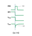
現參考圖3A,在電容耦合之來源中,一種可能的來源可係在資料線304與Vcom線306間之電容(亦即CDC 302)。例如當經由資料線304施加電壓信號時,資料線304中的電壓位準變化可造成資料線304與Vcom線306間的電容耦合效應。另一可能的電容耦合源可發生於儲存電容器之電極與像素電極間。Referring now to FIG. 3A, among the sources of capacitive coupling, one possible source may be the capacitance between the data line 304 and the V com line 306 (ie, C DC 302). For example, when a voltage signal is applied through the data line 304, the change of the voltage level in the data line 304 can cause a capacitive coupling effect between the data line 304 and the V com line 306. Another possible source of capacitive coupling can occur between the electrode of the storage capacitor and the pixel electrode.
操作時,Vcom
電壓值可於選擇顯示像素(亦即掃描線308選擇像素310)且經由資料線304施加驅動電壓信號時經歷擾動(例如電壓值驟降)。在此情況下,部分受前述電容效應影響,Vcom
電壓值可偏移目標值(例如+15、-15或0V)。若當掃描線308關閉時Vcom
無法回到此目標電壓值(亦即將所選顯示像素置於浮動狀態),則所選像素電極之電壓位準將概略偏移目標值至較推估值低,導致沿著Vcom
線方向之可見帶狀。可利用電荷守恆原理計算像素電壓(ΔVPIXEL
)之偏移
其中ΔVCOM 係在掃描線關閉時之Vcom 電壓偏移值,Ctotal 係像素電極的總電容,且Ctotal 除了前述電容耦合效應外,亦可包含任何金屬層與材料層間引發之電容耦合效應。Where ΔV COM is the offset value of the V com voltage when the scan line is turned off , C total is the total capacitance of the pixel electrode, and C total can also include any capacitive coupling effect induced between the metal layer and the material layer in addition to the aforementioned capacitive coupling effect. .
此像素電壓偏移(ΔVPIXEL
)有時可稱之為串擾或雜散。一種緩解這些非所欲效應的方式可降低Vcom
信號之RC延遲,以確保VCOM
值在掃描線啟動期間回到目標值或位準。圖3B例示隨著開啟像素(亦即開啟像素310)之掃描電壓314升高, Vcom
電壓312歷經驟降。This pixel voltage shift ( ΔV PIXEL ) can sometimes be referred to as crosstalk or spurious. A way to alleviate these undesired effects can reduce the RC delay of the V com signal to ensure that the V COM value returns to the target value or level during the start of the scan line. FIG. 3B illustrates that as the
為降低前述RC延遲以確保快速V位準恢復,圖4B中呈現一種新的顯示器背板設計。但首先參考圖4A,其中呈現習知背板400。如圖4A所示,顯示像素的每一列受VCOM
線402偏壓,藉此施加VCOM
電壓至每一像素。圖4A中顯示每一列之VCOM
信號線彼此獨立。在此構造中,當VCOM
值受儲存電容器及資料線導致之電容耦合效應(亦即CDC
)影響或偏移時,可僅藉由在像素陣列兩端施加電壓而恢復VCOM
值,但可能不夠快。In order to reduce the aforementioned RC delay to ensure fast V-level recovery, a new display backplane design is presented in FIG. 4B. But first, referring to FIG. 4A, a
現參考圖4B,在依此處所揭示之主題之設計410中,一VCOM
線412可利用傳導路徑416電耦合至相鄰列之另一VCOM
線414,其中可利用習知用於此技術中之材料建構該傳導路徑416,以建構一導電線(例如銅、金等)。在此構造中,VCOM
電流現可自像素陣列的四側抵達像素,導致RC延遲降低,造成較快速的VCOM
恢復時間。Referring now to FIG. 4B, in the
實際上,一EPD可具有顯示像素之兩相鄰列,其中每一列可包含複數個顯示像素,且每一顯示像素具有用於驅動顯示像素之一像素電極。且每一列亦可具有連接至複數個顯示像素之每一像素電極之第一信號線,及連接顯示像素之第一列之第一信號線至第二列之第二信號線之至少一個傳導路徑。或如圖4B所示,顯示像素之相鄰列間具有超過1個,例如2或3或4個此類傳導路徑。In fact, an EPD may have two adjacent columns of display pixels, where each column may include a plurality of display pixels, and each display pixel has a pixel electrode for driving the display pixels. And each row can also have a first signal line connected to each pixel electrode of a plurality of display pixels, and at least one conductive path connecting the first signal line of the first row of the display pixels to the second signal line of the second row . Or, as shown in FIG. 4B, there are more than one, for example, 2 or 3 or 4 such conduction paths between adjacent rows of display pixels.
在另一實施例中,示如上述的圖2,一EPD可具有相間隔之第一與第二裝置層,及顯示像素之第一與第二列,其中每一列可具有複數個顯示像素,且每一顯示像素具有位於第一裝置層上用於驅動顯示像素之像素電極。此外,一信號線位於第二裝置層上且與複數個顯示像素之像素電極的一部份重疊,及至少一個傳導路徑連接顯示像素之第一列之信號線至第二列之信號線。In another embodiment, as shown in FIG. 2 above, an EPD may have spaced apart first and second device layers, and first and second rows of display pixels, where each row may have a plurality of display pixels, And each display pixel has a pixel electrode located on the first device layer for driving the display pixel. In addition, a signal line is located on the second device layer and overlaps a part of the pixel electrodes of the plurality of display pixels, and at least one conductive path connects the signal line of the first row of the display pixels to the signal line of the second row.
圖5A例示利用圖4A所示背板顯示之影像,其中具串擾效應。經比較,圖5B例示利用圖4B所示背板顯示之影像,其中串擾效應降低。FIG. 5A illustrates an image displayed using the backplane shown in FIG. 4A, which has a crosstalk effect. By comparison, FIG. 5B illustrates an image displayed using the back panel shown in FIG. 4B, in which the crosstalk effect is reduced.
自前述可見本發明可提供用以降低串擾及顯示像素電壓偏移之背板。熟悉此技術者將顯見可在不背離本發明之範疇下,對本發明之特定實施例進行多種改變與變化。因此,前述整體係例示性而無限制之意。From the foregoing, it can be seen that the present invention can provide a backplane for reducing crosstalk and display pixel voltage deviation. Those skilled in the art will obviously be able to make various changes and changes to the specific embodiments of the present invention without departing from the scope of the present invention. Therefore, the aforementioned whole is illustrative and not restrictive.
100:電泳顯示器 102:薄膜電晶體 104:掃描線 106:資料線 108:Vcom 線 200:顯示像素 202:閘極線 204:像素電極 206:資料線 208:電晶體 210:Vcom 線 214:電極 216:閘極 302:CDC 304:資料線 306:Vcom 線 308:掃描線 310:像素 312:Vcom 電壓 314:掃描電壓 400:背板 402:VCOM 線 410:設計 412:VCOM 線 414:VCOM 線 416:傳導路徑100: electrophoretic display 102: thin film transistor 104: scanning line 106: data line 108: V com line 200: display pixel 202: gate line 204: pixel electrode 206: data line 208: transistor 210: V com line 214: Electrode 216: Gate 302: C DC 304: Data line 306: V com line 308: Scan line 310: Pixel 312: V com voltage 314: Scan voltage 400: Backplane 402: V COM line 410: Design 412: V COM Line 414: V COM Line 416: Conduction path
圖1例示依此處所揭示之主題之背板電路; 圖2例示依此處所揭示之主題之顯示像素頂視圖; 圖3A例示依此處所揭示之主題之顯示像素之等效電路實施例; 圖3B例示依此處所揭示之主題之樣本驅動機制; 圖4A例示依此處所揭示之主題之一背板電路; 圖4B例示依此處所揭示之主題之另一背板電路; 圖5A例示依此處所揭示之主題之具串擾(crosstalk)之顯示影像; 圖5B例示利用此處所揭示之主題之具降低串擾之顯示影像。Figure 1 illustrates the backplane circuit according to the subject disclosed here; Figure 2 illustrates a top view of display pixels according to the subject disclosed here; FIG. 3A illustrates an embodiment of an equivalent circuit of a display pixel according to the subject disclosed herein; Figure 3B illustrates a sample-driven mechanism based on the theme disclosed here; FIG. 4A illustrates a backplane circuit according to one of the topics disclosed herein; FIG. 4B illustrates another backplane circuit according to the subject disclosed herein; FIG. 5A illustrates a display image with crosstalk according to the theme disclosed here; FIG. 5B illustrates a display image with crosstalk reduction using the theme disclosed herein.
無。none.
Claims (9)
Applications Claiming Priority (2)
| Application Number | Priority Date | Filing Date | Title |
|---|---|---|---|
| US201862757818P | 2018-11-09 | 2018-11-09 | |
| US62/757,818 | 2018-11-09 |
Publications (2)
| Publication Number | Publication Date |
|---|---|
| TW202103133A TW202103133A (en) | 2021-01-16 |
| TWI733246B true TWI733246B (en) | 2021-07-11 |
Family
ID=70551796
Family Applications (1)
| Application Number | Title | Priority Date | Filing Date |
|---|---|---|---|
| TW108140715A TWI733246B (en) | 2018-11-09 | 2019-11-08 | Electro-optic displays |
Country Status (7)
| Country | Link |
|---|---|
| US (2) | US11145262B2 (en) |
| EP (1) | EP3877808A4 (en) |
| JP (2) | JP7250921B2 (en) |
| KR (2) | KR20230128588A (en) |
| CN (1) | CN112955817A (en) |
| TW (1) | TWI733246B (en) |
| WO (1) | WO2020097462A1 (en) |
Families Citing this family (1)
| Publication number | Priority date | Publication date | Assignee | Title |
|---|---|---|---|---|
| KR20230128588A (en) * | 2018-11-09 | 2023-09-05 | 이 잉크 코포레이션 | Electro-optic displays |
Citations (6)
| Publication number | Priority date | Publication date | Assignee | Title |
|---|---|---|---|---|
| TW200516334A (en) * | 2003-09-08 | 2005-05-16 | Koninkl Philips Electronics Nv | Electrophoretic display activation with blanking frames |
| US20110298727A1 (en) * | 2010-06-07 | 2011-12-08 | Marduke Yousefpor | Touch-display crosstalk |
| TWI394119B (en) * | 2006-12-23 | 2013-04-21 | Lg Display Co Ltd | Electrophoresis display and driving method thereof |
| US8614654B2 (en) * | 2009-07-30 | 2013-12-24 | Apple Inc. | Crosstalk reduction in LCD panels |
| CN104020881A (en) * | 2014-05-29 | 2014-09-03 | 京东方科技集团股份有限公司 | Touch display panel, driving method thereof and display device |
| CN104280969A (en) * | 2014-11-03 | 2015-01-14 | 友达光电股份有限公司 | Liquid crystal panel and manufacturing method thereof |
Family Cites Families (172)
| Publication number | Priority date | Publication date | Assignee | Title |
|---|---|---|---|---|
| US3058659A (en) | 1958-12-31 | 1962-10-16 | Ibm | Add address to memory instruction |
| US3009344A (en) | 1959-12-31 | 1961-11-21 | Claude J Falconer | Diaper washer |
| US7106296B1 (en) | 1995-07-20 | 2006-09-12 | E Ink Corporation | Electronic book with multiple page displays |
| US7411719B2 (en) | 1995-07-20 | 2008-08-12 | E Ink Corporation | Electrophoretic medium and process for the production thereof |
| US7327511B2 (en) | 2004-03-23 | 2008-02-05 | E Ink Corporation | Light modulators |
| US7259744B2 (en) | 1995-07-20 | 2007-08-21 | E Ink Corporation | Dielectrophoretic displays |
| US7167155B1 (en) | 1995-07-20 | 2007-01-23 | E Ink Corporation | Color electrophoretic displays |
| US6639578B1 (en) | 1995-07-20 | 2003-10-28 | E Ink Corporation | Flexible displays |
| US6120588A (en) | 1996-07-19 | 2000-09-19 | E Ink Corporation | Electronically addressable microencapsulated ink and display thereof |
| US7352353B2 (en) | 1995-07-20 | 2008-04-01 | E Ink Corporation | Electrostatically addressable electrophoretic display |
| US6124851A (en) | 1995-07-20 | 2000-09-26 | E Ink Corporation | Electronic book with multiple page displays |
| US6664944B1 (en) | 1995-07-20 | 2003-12-16 | E-Ink Corporation | Rear electrode structures for electrophoretic displays |
| US8089453B2 (en) | 1995-07-20 | 2012-01-03 | E Ink Corporation | Stylus-based addressing structures for displays |
| US6866760B2 (en) | 1998-08-27 | 2005-03-15 | E Ink Corporation | Electrophoretic medium and process for the production thereof |
| CA2260947A1 (en) | 1996-07-19 | 1998-01-29 | E Ink Corporation | Electronically addressable microencapsulated ink and display thereof |
| US5930026A (en) | 1996-10-25 | 1999-07-27 | Massachusetts Institute Of Technology | Nonemissive displays and piezoelectric power supplies therefor |
| US6980196B1 (en) | 1997-03-18 | 2005-12-27 | Massachusetts Institute Of Technology | Printable electronic display |
| US6177921B1 (en) | 1997-08-28 | 2001-01-23 | E Ink Corporation | Printable electrode structures for displays |
| US6232950B1 (en) | 1997-08-28 | 2001-05-15 | E Ink Corporation | Rear electrode structures for displays |
| US7002728B2 (en) | 1997-08-28 | 2006-02-21 | E Ink Corporation | Electrophoretic particles, and processes for the production thereof |
| US6252564B1 (en) | 1997-08-28 | 2001-06-26 | E Ink Corporation | Tiled displays |
| US7075502B1 (en) | 1998-04-10 | 2006-07-11 | E Ink Corporation | Full color reflective display with multichromatic sub-pixels |
| JP4664501B2 (en) | 1998-04-10 | 2011-04-06 | イー インク コーポレイション | Electronic display using organic field effect transistors |
| US6241921B1 (en) | 1998-05-15 | 2001-06-05 | Massachusetts Institute Of Technology | Heterogeneous display elements and methods for their fabrication |
| DE69907744T2 (en) | 1998-06-22 | 2003-11-20 | E Ink Corp | METHOD FOR ADDRESSING MICROCAPSULATED DISPLAY MEDIA |
| EP1099207B1 (en) | 1998-07-22 | 2002-03-27 | E-Ink Corporation | Electronic display |
| USD485294S1 (en) | 1998-07-22 | 2004-01-13 | E Ink Corporation | Electrode structure for an electronic display |
| US7256766B2 (en) | 1998-08-27 | 2007-08-14 | E Ink Corporation | Electrophoretic display comprising optical biasing element |
| CA2346167C (en) | 1998-10-07 | 2007-05-22 | E Ink Corporation | Illumination system for nonemissive electronic displays |
| US6506438B2 (en) | 1998-12-15 | 2003-01-14 | E Ink Corporation | Method for printing of transistor arrays on plastic substrates |
| US6312304B1 (en) | 1998-12-15 | 2001-11-06 | E Ink Corporation | Assembly of microencapsulated electronic displays |
| US6724519B1 (en) | 1998-12-21 | 2004-04-20 | E-Ink Corporation | Protective electrodes for electrophoretic displays |
| WO2000038000A1 (en) | 1998-12-22 | 2000-06-29 | E Ink Corporation | Method of manufacturing of a discrete electronic device |
| TW521241B (en) * | 1999-03-16 | 2003-02-21 | Sony Corp | Liquid crystal display apparatus, its driving method, and liquid crystal display system |
| US6842657B1 (en) | 1999-04-09 | 2005-01-11 | E Ink Corporation | Reactive formation of dielectric layers and protection of organic layers in organic semiconductor device fabrication |
| US6498114B1 (en) | 1999-04-09 | 2002-12-24 | E Ink Corporation | Method for forming a patterned semiconductor film |
| US7012600B2 (en) | 1999-04-30 | 2006-03-14 | E Ink Corporation | Methods for driving bistable electro-optic displays, and apparatus for use therein |
| US8009348B2 (en) | 1999-05-03 | 2011-08-30 | E Ink Corporation | Machine-readable displays |
| US7030412B1 (en) | 1999-05-05 | 2006-04-18 | E Ink Corporation | Minimally-patterned semiconductor devices for display applications |
| US6392786B1 (en) | 1999-07-01 | 2002-05-21 | E Ink Corporation | Electrophoretic medium provided with spacers |
| AU7137800A (en) | 1999-07-21 | 2001-02-13 | E-Ink Corporation | Preferred methods for producing electrical circuit elements used to control an electronic display |
| AU6365900A (en) | 1999-07-21 | 2001-02-13 | E-Ink Corporation | Use of a storage capacitor to enhance the performance of an active matrix drivenelectronic display |
| AU7094400A (en) | 1999-08-31 | 2001-03-26 | E-Ink Corporation | A solvent annealing process for forming a thin semiconductor film with advantageous properties |
| EP1208603A1 (en) | 1999-08-31 | 2002-05-29 | E Ink Corporation | Transistor for an electronically driven display |
| US6672921B1 (en) | 2000-03-03 | 2004-01-06 | Sipix Imaging, Inc. | Manufacturing process for electrophoretic display |
| US7715088B2 (en) | 2000-03-03 | 2010-05-11 | Sipix Imaging, Inc. | Electrophoretic display |
| US6788449B2 (en) | 2000-03-03 | 2004-09-07 | Sipix Imaging, Inc. | Electrophoretic display and novel process for its manufacture |
| AU2001253575A1 (en) | 2000-04-18 | 2001-10-30 | E-Ink Corporation | Process for fabricating thin film transistors |
| US7893435B2 (en) | 2000-04-18 | 2011-02-22 | E Ink Corporation | Flexible electronic circuits and displays including a backplane comprising a patterned metal foil having a plurality of apertures extending therethrough |
| US20020060321A1 (en) | 2000-07-14 | 2002-05-23 | Kazlas Peter T. | Minimally- patterned, thin-film semiconductor devices for display applications |
| US6816147B2 (en) | 2000-08-17 | 2004-11-09 | E Ink Corporation | Bistable electro-optic display, and method for addressing same |
| AU2002250304A1 (en) | 2001-03-13 | 2002-09-24 | E Ink Corporation | Apparatus for displaying drawings |
| US7679814B2 (en) | 2001-04-02 | 2010-03-16 | E Ink Corporation | Materials for use in electrophoretic displays |
| CN1282027C (en) | 2001-04-02 | 2006-10-25 | 伊英克公司 | Electrophoretic medium with improved image stability |
| US20020188053A1 (en) | 2001-06-04 | 2002-12-12 | Sipix Imaging, Inc. | Composition and process for the sealing of microcups in roll-to-roll display manufacturing |
| US6982178B2 (en) | 2002-06-10 | 2006-01-03 | E Ink Corporation | Components and methods for use in electro-optic displays |
| US7110163B2 (en) | 2001-07-09 | 2006-09-19 | E Ink Corporation | Electro-optic display and lamination adhesive for use therein |
| EP1407320B1 (en) | 2001-07-09 | 2006-12-20 | E Ink Corporation | Electro-optic display and adhesive composition |
| EP1415193B1 (en) | 2001-07-09 | 2012-03-14 | E Ink Corporation | Electro-optical display having a lamination adhesive layer |
| US7535624B2 (en) | 2001-07-09 | 2009-05-19 | E Ink Corporation | Electro-optic display and materials for use therein |
| US6967640B2 (en) | 2001-07-27 | 2005-11-22 | E Ink Corporation | Microencapsulated electrophoretic display with integrated driver |
| JP4353660B2 (en) * | 2001-07-27 | 2009-10-28 | 三洋電機株式会社 | Active matrix display device |
| US6819471B2 (en) | 2001-08-16 | 2004-11-16 | E Ink Corporation | Light modulation by frustration of total internal reflection |
| AU2002357842A1 (en) | 2001-12-13 | 2003-06-23 | E Ink Corporation | Electrophoretic electronic displays with films having a low index of refraction |
| US6885146B2 (en) * | 2002-03-14 | 2005-04-26 | Semiconductor Energy Laboratory Co., Ltd. | Display device comprising substrates, contrast medium and barrier layers between contrast medium and each of substrates |
| US7223672B2 (en) | 2002-04-24 | 2007-05-29 | E Ink Corporation | Processes for forming backplanes for electro-optic displays |
| US7190008B2 (en) | 2002-04-24 | 2007-03-13 | E Ink Corporation | Electro-optic displays, and components for use therein |
| US7116318B2 (en) | 2002-04-24 | 2006-10-03 | E Ink Corporation | Backplanes for display applications, and components for use therein |
| TWI240842B (en) | 2002-04-24 | 2005-10-01 | Sipix Imaging Inc | Matrix driven electrophoretic display with multilayer back plane |
| TW574538B (en) | 2002-04-24 | 2004-02-01 | Sipix Imaging Inc | Compositions and processes for format flexible roll-to-roll manufacturing of electrophoretic displays |
| TW583497B (en) | 2002-05-29 | 2004-04-11 | Sipix Imaging Inc | Electrode and connecting designs for roll-to-roll format flexible display manufacturing |
| US8049947B2 (en) | 2002-06-10 | 2011-11-01 | E Ink Corporation | Components and methods for use in electro-optic displays |
| US7554712B2 (en) | 2005-06-23 | 2009-06-30 | E Ink Corporation | Edge seals for, and processes for assembly of, electro-optic displays |
| US7583427B2 (en) | 2002-06-10 | 2009-09-01 | E Ink Corporation | Components and methods for use in electro-optic displays |
| US7649674B2 (en) | 2002-06-10 | 2010-01-19 | E Ink Corporation | Electro-optic display with edge seal |
| US6842279B2 (en) | 2002-06-27 | 2005-01-11 | E Ink Corporation | Illumination system for nonemissive electronic displays |
| US8547628B2 (en) | 2002-07-17 | 2013-10-01 | Sipix Imaging, Inc. | Methods and compositions for improved electrophoretic display performance |
| US20060255322A1 (en) | 2002-07-17 | 2006-11-16 | Wu Zarng-Arh G | Methods and compositions for improved electrophoretic display performance |
| TWI314237B (en) | 2002-07-17 | 2009-09-01 | Sipix Imaging Inc | Novel methods and compositions for improved electrophoretic display performance |
| US7347957B2 (en) | 2003-07-10 | 2008-03-25 | Sipix Imaging, Inc. | Methods and compositions for improved electrophoretic display performance |
| EP1527371B1 (en) | 2002-08-06 | 2012-10-03 | E Ink Corporation | Protection of electro-optic displays against thermal effects |
| US7839564B2 (en) | 2002-09-03 | 2010-11-23 | E Ink Corporation | Components and methods for use in electro-optic displays |
| TW575646B (en) | 2002-09-04 | 2004-02-11 | Sipix Imaging Inc | Novel adhesive and sealing layers for electrophoretic displays |
| TWI229230B (en) | 2002-10-31 | 2005-03-11 | Sipix Imaging Inc | An improved electrophoretic display and novel process for its manufacture |
| AU2003299673A1 (en) | 2002-12-16 | 2004-07-22 | E Ink Corporation | Backplanes for electro-optic displays |
| US6922276B2 (en) | 2002-12-23 | 2005-07-26 | E Ink Corporation | Flexible electro-optic displays |
| EP1616217B1 (en) | 2003-03-27 | 2010-10-20 | E Ink Corporation | Electro-optic assemblies |
| WO2005002305A2 (en) | 2003-06-06 | 2005-01-06 | Sipix Imaging, Inc. | In mold manufacture of an object with embedded display panel |
| US20050122563A1 (en) | 2003-07-24 | 2005-06-09 | E Ink Corporation | Electro-optic displays |
| US8514168B2 (en) | 2003-10-07 | 2013-08-20 | Sipix Imaging, Inc. | Electrophoretic display with thermal control |
| US20050122306A1 (en) | 2003-10-29 | 2005-06-09 | E Ink Corporation | Electro-optic displays with single edge addressing and removable driver circuitry |
| US20110187683A1 (en) | 2003-10-30 | 2011-08-04 | E Ink Corporation | Electro-optic displays with single edge addressing and removable driver circuitry |
| US7551346B2 (en) | 2003-11-05 | 2009-06-23 | E Ink Corporation | Electro-optic displays, and materials for use therein |
| US8177942B2 (en) | 2003-11-05 | 2012-05-15 | E Ink Corporation | Electro-optic displays, and materials for use therein |
| US7672040B2 (en) | 2003-11-05 | 2010-03-02 | E Ink Corporation | Electro-optic displays, and materials for use therein |
| US20110164301A1 (en) | 2003-11-05 | 2011-07-07 | E Ink Corporation | Electro-optic displays, and materials for use therein |
| EP2487674B1 (en) | 2003-11-05 | 2018-02-21 | E Ink Corporation | Electro-optic displays |
| US7206119B2 (en) | 2003-12-31 | 2007-04-17 | E Ink Corporation | Electro-optic displays, and method for driving same |
| US7075703B2 (en) | 2004-01-16 | 2006-07-11 | E Ink Corporation | Process for sealing electro-optic displays |
| US7388572B2 (en) | 2004-02-27 | 2008-06-17 | E Ink Corporation | Backplanes for electro-optic displays |
| US7453445B2 (en) | 2004-08-13 | 2008-11-18 | E Ink Corproation | Methods for driving electro-optic displays |
| US7301693B2 (en) | 2004-08-13 | 2007-11-27 | Sipix Imaging, Inc. | Direct drive display with a multi-layer backplane and process for its manufacture |
| US7304780B2 (en) | 2004-12-17 | 2007-12-04 | Sipix Imaging, Inc. | Backplane design for display panels and processes for their manufacture |
| US7230751B2 (en) | 2005-01-26 | 2007-06-12 | E Ink Corporation | Electrophoretic displays using gaseous fluids |
| US8576162B2 (en) | 2005-03-14 | 2013-11-05 | Sipix Imaging, Inc. | Manufacturing processes of backplane for segment displays |
| US8159636B2 (en) | 2005-04-08 | 2012-04-17 | Sipix Imaging, Inc. | Reflective displays and processes for their manufacture |
| US7880958B2 (en) | 2005-09-23 | 2011-02-01 | Sipix Imaging, Inc. | Display cell structure and electrode protecting layer compositions |
| US8610988B2 (en) | 2006-03-09 | 2013-12-17 | E Ink Corporation | Electro-optic display with edge seal |
| US20150005720A1 (en) | 2006-07-18 | 2015-01-01 | E Ink California, Llc | Electrophoretic display |
| US7492497B2 (en) | 2006-08-02 | 2009-02-17 | E Ink Corporation | Multi-layer light modulator |
| US8362488B2 (en) | 2006-09-12 | 2013-01-29 | Sipix Imaging, Inc. | Flexible backplane and methods for its manufacture |
| US7986450B2 (en) | 2006-09-22 | 2011-07-26 | E Ink Corporation | Electro-optic display and materials for use therein |
| US7905977B2 (en) | 2006-11-17 | 2011-03-15 | Sipix Imaging, Inc. | Post conversion methods for display devices |
| US8018428B2 (en) | 2006-11-27 | 2011-09-13 | Samsung Electronics Co., Ltd. | Electrophoretic display panel, electrophoretic display device having the same and method for driving the same |
| KR101362389B1 (en) * | 2006-11-27 | 2014-02-12 | 삼성디스플레이 주식회사 | Electro-phoretic display panel, electro-phoretic display device having the same and method for driving the same |
| US7688497B2 (en) | 2007-01-22 | 2010-03-30 | E Ink Corporation | Multi-layer sheet for use in electro-optic displays |
| CN101836167B (en) | 2007-01-22 | 2013-11-06 | 伊英克公司 | Multi-layer sheet for use in electro-optic displays |
| US7826129B2 (en) | 2007-03-06 | 2010-11-02 | E Ink Corporation | Materials for use in electrophoretic displays |
| JP2008233149A (en) * | 2007-03-16 | 2008-10-02 | Seiko Epson Corp | Electrooptical device, electronic equipment, and method for manufacturing electrooptical device |
| JP2008293405A (en) | 2007-05-28 | 2008-12-04 | Fuji Xerox Co Ltd | Data input system |
| US8034209B2 (en) | 2007-06-29 | 2011-10-11 | E Ink Corporation | Electro-optic displays, and materials and methods for production thereof |
| US8743077B1 (en) | 2007-08-01 | 2014-06-03 | Sipix Imaging, Inc. | Front light system for reflective displays |
| US20090122389A1 (en) | 2007-11-14 | 2009-05-14 | E Ink Corporation | Electro-optic assemblies, and adhesives and binders for use therein |
| US7830592B1 (en) | 2007-11-30 | 2010-11-09 | Sipix Imaging, Inc. | Display devices having micro-reflectors |
| US8237892B1 (en) | 2007-11-30 | 2012-08-07 | Sipix Imaging, Inc. | Display device with a brightness enhancement structure |
| US8437069B2 (en) | 2008-03-11 | 2013-05-07 | Sipix Imaging, Inc. | Luminance enhancement structure for reflective display devices |
| CN105137643A (en) | 2008-03-11 | 2015-12-09 | 希毕克斯影像有限公司 | Luminance enhancement structure for reflective display devices |
| US8072675B2 (en) | 2008-05-01 | 2011-12-06 | Sipix Imaging, Inc. | Color display devices |
| US8441414B2 (en) | 2008-12-05 | 2013-05-14 | Sipix Imaging, Inc. | Luminance enhancement structure with Moiré reducing design |
| KR101309364B1 (en) | 2008-12-24 | 2013-09-17 | 엘지디스플레이 주식회사 | Electrophoretic Display Device and Method for manufacturing the same and Method for Repairing the same |
| US8797258B2 (en) | 2008-12-30 | 2014-08-05 | Sipix Imaging, Inc. | Highlight color display architecture using enhanced dark state |
| US20160077375A1 (en) | 2009-01-13 | 2016-03-17 | E Ink California, Llc | Asymmetrical luminance enhancement structure for reflective display devices |
| US20100177396A1 (en) | 2009-01-13 | 2010-07-15 | Craig Lin | Asymmetrical luminance enhancement structure for reflective display devices |
| US9025234B2 (en) | 2009-01-22 | 2015-05-05 | E Ink California, Llc | Luminance enhancement structure with varying pitches |
| US8120836B2 (en) | 2009-03-09 | 2012-02-21 | Sipix Imaging, Inc. | Luminance enhancement structure for reflective display devices |
| US8714780B2 (en) | 2009-04-22 | 2014-05-06 | Sipix Imaging, Inc. | Display devices with grooved luminance enhancement film |
| US8797633B1 (en) | 2009-07-23 | 2014-08-05 | Sipix Imaging, Inc. | Display device assembly and manufacture thereof |
| US8456589B1 (en) | 2009-07-27 | 2013-06-04 | Sipix Imaging, Inc. | Display device assembly |
| US8754859B2 (en) | 2009-10-28 | 2014-06-17 | E Ink Corporation | Electro-optic displays with touch sensors and/or tactile feedback |
| WO2011097228A2 (en) | 2010-02-02 | 2011-08-11 | E Ink Corporation | Method for driving electro-optic displays |
| US8633889B2 (en) | 2010-04-15 | 2014-01-21 | Semiconductor Energy Laboratory Co., Ltd. | Display device, driving method thereof, and electronic appliance |
| US9140952B2 (en) | 2010-04-22 | 2015-09-22 | E Ink California, Llc | Electrophoretic display with enhanced contrast |
| US9030374B2 (en) | 2010-05-06 | 2015-05-12 | E Ink California, Llc | Composite display modules |
| TW201207535A (en) | 2010-05-27 | 2012-02-16 | E Ink Corp | Dual mode electro-optic displays |
| WO2012063830A1 (en) * | 2010-11-09 | 2012-05-18 | シャープ株式会社 | Liquid crystal display device, display device, and gate signal line drive method |
| TW201235758A (en) | 2011-02-24 | 2012-09-01 | Ind Tech Res Inst | Pixel structure, driving method and driving system of hybrid display device |
| TWI582509B (en) | 2012-03-26 | 2017-05-11 | 達意科技股份有限公司 | Electrophoretic display and structure thereof |
| WO2013159093A1 (en) | 2012-04-20 | 2013-10-24 | E Ink Corporation | Illumination systems for reflective displays |
| KR102022698B1 (en) * | 2012-05-31 | 2019-11-05 | 삼성디스플레이 주식회사 | Display panel |
| WO2013191983A1 (en) | 2012-06-20 | 2013-12-27 | Sipix Imaging, Inc. | Piezo electrophoretic display |
| US8797636B2 (en) | 2012-07-17 | 2014-08-05 | Sipix Imaging, Inc. | Light-enhancing structure for electrophoretic display |
| EP2877895B1 (en) | 2012-07-27 | 2017-09-06 | E Ink Corporation | Processes for the production of electro-optic displays |
| US9279906B2 (en) | 2012-08-31 | 2016-03-08 | E Ink California, Llc | Microstructure film |
| TWI478327B (en) | 2012-11-01 | 2015-03-21 | Sipix Technology Inc | Display device |
| US10037735B2 (en) | 2012-11-16 | 2018-07-31 | E Ink Corporation | Active matrix display with dual driving modes |
| TW201428569A (en) | 2013-01-10 | 2014-07-16 | Sipix Technology Inc | Display system having electrophoretic touch panel |
| TWI502265B (en) | 2013-01-25 | 2015-10-01 | Sipix Technology Inc | Electrophoretic display |
| US9666142B2 (en) | 2013-02-20 | 2017-05-30 | Sipix Technology, Inc. | Display capable of reducing passive matrix coupling effect |
| TWI502266B (en) | 2013-02-20 | 2015-10-01 | Sipix Technology Inc | Electrophoretic display capable of reducing passive matrix coupling effect |
| TWI502429B (en) | 2013-06-13 | 2015-10-01 | Sipix Technology Inc | Touch-control display and fabrication method thereof |
| TWI532599B (en) | 2013-06-21 | 2016-05-11 | 達意科技股份有限公司 | Display panel and manufacturing method of display panel |
| US9223164B2 (en) | 2013-08-02 | 2015-12-29 | Sipix Technology, Inc. | Display |
| TWI502574B (en) | 2013-10-09 | 2015-10-01 | Sipix Technology Inc | Electro-optical apparatus and driving method thereof |
| KR101883582B1 (en) | 2014-01-17 | 2018-07-30 | 이 잉크 코포레이션 | Electro-optic display with a two-phase electrode layer |
| CN106133816A (en) | 2014-02-07 | 2016-11-16 | 伊英克公司 | The back board structure of electro-optic displays |
| US10446585B2 (en) | 2014-03-17 | 2019-10-15 | E Ink Corporation | Multi-layer expanding electrode structures for backplane assemblies |
| US10444553B2 (en) | 2014-03-25 | 2019-10-15 | E Ink California, Llc | Magnetophoretic display assembly and driving scheme |
| TWI613498B (en) | 2014-06-27 | 2018-02-01 | 電子墨水加利福尼亞有限責任公司 | Anisotropic conductive dielectric layer for electrophoretic display |
| US20160012710A1 (en) | 2014-07-10 | 2016-01-14 | Sipix Technology Inc. | Smart medication device |
| US20160018710A1 (en) * | 2014-07-21 | 2016-01-21 | Li Chai | Display panel, array substrate and method for manufacturing the same |
| KR101958587B1 (en) * | 2015-01-05 | 2019-03-14 | 이 잉크 코포레이션 | Electro-optic displays, and methods for driving same |
| KR20230128588A (en) * | 2018-11-09 | 2023-09-05 | 이 잉크 코포레이션 | Electro-optic displays |
-
2019
- 2019-11-08 KR KR1020237029211A patent/KR20230128588A/en not_active Application Discontinuation
- 2019-11-08 EP EP19882567.1A patent/EP3877808A4/en active Pending
- 2019-11-08 WO PCT/US2019/060470 patent/WO2020097462A1/en unknown
- 2019-11-08 KR KR1020217016478A patent/KR102576895B1/en active IP Right Grant
- 2019-11-08 US US16/678,323 patent/US11145262B2/en active Active
- 2019-11-08 TW TW108140715A patent/TWI733246B/en active
- 2019-11-08 CN CN201980070491.8A patent/CN112955817A/en active Pending
- 2019-11-08 JP JP2021522394A patent/JP7250921B2/en active Active
-
2021
- 2021-10-07 US US17/496,749 patent/US11450287B2/en active Active
-
2022
- 2022-10-03 JP JP2022159462A patent/JP2022173518A/en not_active Withdrawn
Patent Citations (6)
| Publication number | Priority date | Publication date | Assignee | Title |
|---|---|---|---|---|
| TW200516334A (en) * | 2003-09-08 | 2005-05-16 | Koninkl Philips Electronics Nv | Electrophoretic display activation with blanking frames |
| TWI394119B (en) * | 2006-12-23 | 2013-04-21 | Lg Display Co Ltd | Electrophoresis display and driving method thereof |
| US8614654B2 (en) * | 2009-07-30 | 2013-12-24 | Apple Inc. | Crosstalk reduction in LCD panels |
| US20110298727A1 (en) * | 2010-06-07 | 2011-12-08 | Marduke Yousefpor | Touch-display crosstalk |
| CN104020881A (en) * | 2014-05-29 | 2014-09-03 | 京东方科技集团股份有限公司 | Touch display panel, driving method thereof and display device |
| CN104280969A (en) * | 2014-11-03 | 2015-01-14 | 友达光电股份有限公司 | Liquid crystal panel and manufacturing method thereof |
Also Published As
| Publication number | Publication date |
|---|---|
| US11145262B2 (en) | 2021-10-12 |
| US11450287B2 (en) | 2022-09-20 |
| JP2022173518A (en) | 2022-11-18 |
| KR20230128588A (en) | 2023-09-05 |
| KR102576895B1 (en) | 2023-09-08 |
| US20200152140A1 (en) | 2020-05-14 |
| WO2020097462A1 (en) | 2020-05-14 |
| TW202103133A (en) | 2021-01-16 |
| JP2022505740A (en) | 2022-01-14 |
| KR20210068596A (en) | 2021-06-09 |
| JP7250921B2 (en) | 2023-04-03 |
| EP3877808A1 (en) | 2021-09-15 |
| CN112955817A (en) | 2021-06-11 |
| US20220028347A1 (en) | 2022-01-27 |
| EP3877808A4 (en) | 2022-07-27 |
Similar Documents
| Publication | Publication Date | Title |
|---|---|---|
| JP7438314B2 (en) | electro-optical display | |
| TWI728631B (en) | Electro-optic displays | |
| US20170343876A1 (en) | Backplanes for Electro-Optic Displays | |
| TWI733246B (en) | Electro-optic displays | |
| US20220398956A1 (en) | Methods and apparatuses for driving electro-optic displays | |
| US20180102081A1 (en) | Driving methods for electro-optic displays | |
| RU2783032C1 (en) | Electro-optical displays |