RU2661891C2 - Driver circuit between electromagnetic ballast and light-emitting diode - Google Patents
Driver circuit between electromagnetic ballast and light-emitting diode Download PDFInfo
- Publication number
- RU2661891C2 RU2661891C2 RU2015102286A RU2015102286A RU2661891C2 RU 2661891 C2 RU2661891 C2 RU 2661891C2 RU 2015102286 A RU2015102286 A RU 2015102286A RU 2015102286 A RU2015102286 A RU 2015102286A RU 2661891 C2 RU2661891 C2 RU 2661891C2
- Authority
- RU
- Russia
- Prior art keywords
- current signal
- circuit
- value
- parameter
- diode elements
- Prior art date
Links
Images
Classifications
-
- H—ELECTRICITY
- H05—ELECTRIC TECHNIQUES NOT OTHERWISE PROVIDED FOR
- H05B—ELECTRIC HEATING; ELECTRIC LIGHT SOURCES NOT OTHERWISE PROVIDED FOR; CIRCUIT ARRANGEMENTS FOR ELECTRIC LIGHT SOURCES, IN GENERAL
- H05B45/00—Circuit arrangements for operating light-emitting diodes [LED]
- H05B45/50—Circuit arrangements for operating light-emitting diodes [LED] responsive to malfunctions or undesirable behaviour of LEDs; responsive to LED life; Protective circuits
- H05B45/56—Circuit arrangements for operating light-emitting diodes [LED] responsive to malfunctions or undesirable behaviour of LEDs; responsive to LED life; Protective circuits involving measures to prevent abnormal temperature of the LEDs
-
- H—ELECTRICITY
- H05—ELECTRIC TECHNIQUES NOT OTHERWISE PROVIDED FOR
- H05B—ELECTRIC HEATING; ELECTRIC LIGHT SOURCES NOT OTHERWISE PROVIDED FOR; CIRCUIT ARRANGEMENTS FOR ELECTRIC LIGHT SOURCES, IN GENERAL
- H05B44/00—Circuit arrangements for operating electroluminescent light sources
-
- H—ELECTRICITY
- H05—ELECTRIC TECHNIQUES NOT OTHERWISE PROVIDED FOR
- H05B—ELECTRIC HEATING; ELECTRIC LIGHT SOURCES NOT OTHERWISE PROVIDED FOR; CIRCUIT ARRANGEMENTS FOR ELECTRIC LIGHT SOURCES, IN GENERAL
- H05B47/00—Circuit arrangements for operating light sources in general, i.e. where the type of light source is not relevant
- H05B47/20—Responsive to malfunctions or to light source life; for protection
- H05B47/25—Circuit arrangements for protecting against overcurrent
-
- H—ELECTRICITY
- H05—ELECTRIC TECHNIQUES NOT OTHERWISE PROVIDED FOR
- H05B—ELECTRIC HEATING; ELECTRIC LIGHT SOURCES NOT OTHERWISE PROVIDED FOR; CIRCUIT ARRANGEMENTS FOR ELECTRIC LIGHT SOURCES, IN GENERAL
- H05B41/00—Circuit arrangements or apparatus for igniting or operating discharge lamps
- H05B41/14—Circuit arrangements
- H05B41/26—Circuit arrangements in which the lamp is fed by power derived from dc by means of a converter, e.g. by high-voltage dc
- H05B41/28—Circuit arrangements in which the lamp is fed by power derived from dc by means of a converter, e.g. by high-voltage dc using static converters
- H05B41/295—Circuit arrangements in which the lamp is fed by power derived from dc by means of a converter, e.g. by high-voltage dc using static converters with semiconductor devices and specially adapted for lamps with preheating electrodes, e.g. for fluorescent lamps
- H05B41/298—Arrangements for protecting lamps or circuits against abnormal operating conditions
- H05B41/2981—Arrangements for protecting lamps or circuits against abnormal operating conditions for protecting the circuit against abnormal operating conditions
- H05B41/2983—Arrangements for protecting lamps or circuits against abnormal operating conditions for protecting the circuit against abnormal operating conditions against abnormal power supply conditions
-
- Y—GENERAL TAGGING OF NEW TECHNOLOGICAL DEVELOPMENTS; GENERAL TAGGING OF CROSS-SECTIONAL TECHNOLOGIES SPANNING OVER SEVERAL SECTIONS OF THE IPC; TECHNICAL SUBJECTS COVERED BY FORMER USPC CROSS-REFERENCE ART COLLECTIONS [XRACs] AND DIGESTS
- Y02—TECHNOLOGIES OR APPLICATIONS FOR MITIGATION OR ADAPTATION AGAINST CLIMATE CHANGE
- Y02B—CLIMATE CHANGE MITIGATION TECHNOLOGIES RELATED TO BUILDINGS, e.g. HOUSING, HOUSE APPLIANCES OR RELATED END-USER APPLICATIONS
- Y02B20/00—Energy efficient lighting technologies, e.g. halogen lamps or gas discharge lamps
- Y02B20/30—Semiconductor lamps, e.g. solid state lamps [SSL] light emitting diodes [LED] or organic LED [OLED]
Landscapes
- Physics & Mathematics (AREA)
- Engineering & Computer Science (AREA)
- Microelectronics & Electronic Packaging (AREA)
- Optics & Photonics (AREA)
- Circuit Arrangement For Electric Light Sources In General (AREA)
- Rectifiers (AREA)
- Led Devices (AREA)
- Electroluminescent Light Sources (AREA)
Abstract
Description
ОБЛАСТЬ ТЕХНИКИ, К КОТОРОЙ ОТНОСИТСЯ ИЗОБРЕТЕНИЕFIELD OF THE INVENTION
Изобретение относится к схеме возбуждения для подключения электромагнитного балласта к осветительной схеме, содержащей один или более светодиодов. Изобретение также относится к устройству, содержащему схему возбуждения и дополнительно содержащему электромагнитный балласт и/или осветительную схему.The invention relates to an excitation circuit for connecting an electromagnetic ballast to a lighting circuit comprising one or more LEDs. The invention also relates to a device comprising an excitation circuit and further comprising an electromagnetic ballast and / or a lighting circuit.
Примерами такой схемы возбуждения являются мостовые выпрямители. Примерами такого устройства являются электромагнитные балласты, лампы и их части.Examples of such a drive circuit are bridge rectifiers. Examples of such a device are electromagnetic ballasts, lamps, and parts thereof.
УРОВЕНЬ ТЕХНИКИBACKGROUND
При замене газоразрядных ламп, например люминесцентных ламп, осветительными схемами, содержащими один или более светодиодов, иногда электромагнитные балласты, необходимые для возбуждения газоразрядных ламп, нельзя заменять или удалять или не следует заменять или удалять. В этом случае, схема возбуждения, возможно, вызовет повреждение этого электромагнитного балласта, когда схема возбуждения возбуждает осветительную схему, содержащую один или более светодиодов.When replacing discharge lamps, such as fluorescent lamps, with lighting circuits containing one or more LEDs, sometimes the electromagnetic ballasts necessary to drive the discharge lamps cannot be replaced or removed, or should not be replaced or removed. In this case, the excitation circuit may cause damage to this electromagnetic ballast when the excitation circuit excites an illumination circuit containing one or more LEDs.
В WO 2006/102355 A2 раскрыт преобразователь мощности для возбуждения, по меньшей мере, одного светодиода. Преобразователь мощности принимает переменный ток от источника питания и включает в себя фильтр электромагнитных помех (ФЭМП), выпрямитель и силовой блок. Силовой блок содержит защитную схему для защиты силового блока от сверхтока или условий короткого замыкания. Защитная схема не обеспечивает защиты электромагнитного балласта, который может быть подключен к входу выпрямителя или к входу фильтра электромагнитных помех.WO 2006/102355 A2 discloses a power converter for driving at least one LED. The power converter receives alternating current from the power source and includes an electromagnetic interference filter (FEMP), a rectifier and a power unit. The power unit contains a protective circuit to protect the power unit from overcurrent or short circuit conditions. The protective circuit does not protect the electromagnetic ballast, which can be connected to the input of the rectifier or to the input of the electromagnetic interference filter.
РАСКРЫТИЕ ИЗОБРЕТЕНИЯSUMMARY OF THE INVENTION
Задачей изобретения является обеспечение усовершенствованной схемы возбуждения. Еще одной задачей изобретения является обеспечение усовершенствованного устройства.The objective of the invention is to provide an improved excitation circuit. Another objective of the invention is the provision of an improved device.
Согласно первому аспекту, предусмотрена схема возбуждения для подключения электромагнитного балласта к осветительной схеме содержащая один или более светодиодов, причем схема возбуждения содержитAccording to a first aspect, an excitation circuit is provided for connecting an electromagnetic ballast to a lighting circuit comprising one or more LEDs, the excitation circuit comprising
- мостовой выпрямитель, имеющий вход для обмена первым сигналом тока с электромагнитным балластом и выход для подачи второго сигнала тока на осветительную схему, иa bridge rectifier having an input for exchanging a first current signal with an electromagnetic ballast and an output for supplying a second current signal to a lighting circuit, and
- защитную схему для защиты электромагнитного балласта от получения одним или более параметрами первого сигнала тока значения, превышающего пороговое значение.- a protective circuit for protecting the electromagnetic ballast from receiving by one or more parameters of the first current signal a value that exceeds a threshold value.
Благодаря снабжению схемы возбуждения, помимо выпрямительной схемы, защитной схемой, электромагнитный балласт защищается от получения параметром первого сигнала тока значения, превышающего пороговое значение.Thanks to the supply of the excitation circuit, in addition to the rectifier circuit, a protective circuit, the electromagnetic ballast is protected from receiving the parameter of the first current signal of a value exceeding the threshold value.
Следует понимать, что получение параметром первого сигнала тока значения, превышающего пороговое значение, может вызывать повреждение электромагнитного балласта.It should be understood that the receipt by the parameter of the first current signal of a value exceeding the threshold value may cause damage to the electromagnetic ballast.
Основная идея состоит в том, что схема возбуждения должна быть снабжена защитной схемой для защиты электромагнитного балласта от получения параметром первого сигнала тока значения, превышающего пороговое значение.The main idea is that the excitation circuit should be equipped with a protective circuit to protect the electromagnetic ballast from receiving the parameter of the first current signal of a value exceeding the threshold value.
Осветительная схема содержит один или более светодиодов любого вида и в любой комбинации.The lighting circuit contains one or more LEDs of any kind and in any combination.
Вариант осуществления схемы возбуждения определяется тем, что параметр является составляющей постоянного тока первого сигнала тока. Слишком большая составляющая постоянного тока или DC-составляющая в первом сигнале тока может приводить к насыщению и, таким образом, к перегреву электромагнитного балласта. Это может приводить к повреждению электромагнитного балласта и его окружения.An embodiment of the drive circuit is determined by the fact that the parameter is a DC component of the first current signal. Too large a DC component or DC component in the first current signal can lead to saturation and, thus, to overheating of the electromagnetic ballast. This can damage the electromagnetic ballast and its surroundings.
Вариант осуществления схемы возбуждения определяется тем, что мостовой выпрямитель содержит четыре первых диодных элемента, защитная схема содержит четыре вторых диодных элемента, причем соответствующие первые диодные элементы последовательно подключены к соответствующим вторым диодным элементам. Выпрямительная схема, состоящая из четырежды два или более последовательно соединенных диодных элемента, образует хорошую защиту от выхода из строя одного из диодных элементов, при котором он превращается в так называемый короткозамыкатель. Диодный элемент, который, в результате выхода из строя, превращается в короткозамыкатель, обладает слишком низким значением импеданса в своем запирающем направлении. В случае, когда один из последовательно соединенных диодных элементов обладает слишком низким значением импеданса в своем запирающем направлении, другой из последовательно соединенных диодных элементов будет сохранять свою нормальную импедансную характеристику и будет блокировать обратный ток. В результате, комбинация мостового выпрямителя и защитной схемы сохранит свою выпрямительную функцию. При этом первый и/или второй сигнал тока приобретет слегка асимметричную форму вследствие аномальной импедансной характеристики отказавшего диодного элемента, и, в результате, DC-составляющая в этом сигнале тока приобретет значение, чуть большее нуля, но это значение все еще будет не настолько велико, чтобы вызвать повреждение электромагнитного балласта.An embodiment of the drive circuit is determined by the fact that the bridge rectifier contains four first diode elements, the protective circuit contains four second diode elements, and the corresponding first diode elements are connected in series to the corresponding second diode elements. The rectifier circuit, consisting of four times two or more series-connected diode elements, forms good protection against the failure of one of the diode elements, in which it turns into a so-called short circuit. The diode element, which, as a result of failure, turns into a short circuit, has an too low impedance value in its locking direction. In the case when one of the series-connected diode elements has an too low impedance value in its blocking direction, the other of the series-connected diode elements will maintain its normal impedance characteristic and will block the reverse current. As a result, the combination of a bridge rectifier and a protective circuit will retain its rectifier function. In this case, the first and / or second current signal will acquire a slightly asymmetric shape due to the anomalous impedance characteristic of the failed diode element, and, as a result, the DC component in this current signal will acquire a value slightly greater than zero, but this value will still not be so large. to cause damage to the electromagnetic ballast.
Диодный элемент содержит диод, или стабилитрон, или транзистор, или его часть. В случае двух или более последовательно соединенных диодных элемента, каждый из них может содержать диод или стабилитрон или транзистор или его часть.The diode element contains a diode, or a zener diode, or a transistor, or part thereof. In the case of two or more series-connected diode elements, each of them may contain a diode or a zener diode or transistor or part thereof.
Вариант осуществления схемы возбуждения определяется тем, что параметр является средним значением выпрямленной версии первого сигнала тока. Слишком большое среднее значение выпрямленной версии первого сигнала тока может приводить к перегреву электромагнитного балласта. Это может приводить к повреждению электромагнитного балласта и его окружения. Среднее значение выпрямленного первого сигнала тока может представлять среднеквадратическое значение этого первого сигнала тока.An embodiment of the drive circuit is determined by the fact that the parameter is the average value of the rectified version of the first current signal. Too large an average value of the rectified version of the first current signal can lead to overheating of the electromagnetic ballast. This can damage the electromagnetic ballast and its surroundings. The average value of the rectified first current signal may represent the rms value of this first current signal.
Вариант осуществления схемы возбуждения определяется тем, что защитная схема содержит детектор для детектирования среднего значения выпрямленной версии первого сигнала тока или среднего значения второго сигнала тока и содержит переключатель для прерывания второго сигнала тока в соответствии с результатом детектирования. Детектирование среднего значения второго сигнала тока является альтернативой детектированию среднего значения выпрямленной версии первого сигнала тока.An embodiment of the drive circuit is determined by the fact that the protective circuit includes a detector for detecting the average value of the rectified version of the first current signal or the average value of the second current signal and comprises a switch for interrupting the second current signal in accordance with the detection result. Detecting the average value of the second current signal is an alternative to detecting the average value of the rectified version of the first current signal.
Вариант осуществления схемы возбуждения определяется тем, что параметр является пиковым значением первого сигнала тока. Слишком большое пиковое значение первого сигнала тока может приводить к перегреву электромагнитного балласта. Это может приводить к повреждению электромагнитного балласта и его окружения.An embodiment of the drive circuit is determined by the fact that the parameter is a peak value of the first current signal. Too high peak value of the first current signal can lead to overheating of the electromagnetic ballast. This can damage the electromagnetic ballast and its surroundings.
Вариант осуществления схемы возбуждения определяется тем, что защитная схема содержит детектор для детектирования пикового значения первого сигнала тока или пикового значения второго сигнала тока и содержит переключатель для прерывания второго сигнала тока в соответствии с результатом детектирования. Слишком большое пиковое значение первого и/или второго сигнала тока может быть обусловлено выходом из строя диодного элемента, при котором он превращается в так называемый разрыв. Диодный элемент, который, в результате выхода из строя, превращается в разрыв, обладает чрезмерно большим значением импеданса в своем проводящем направлении. Детектирование пикового значения второго сигнала тока является альтернативой детектированию пикового значения первого сигнала тока.An embodiment of the drive circuit is determined by the fact that the protective circuit includes a detector for detecting the peak value of the first current signal or the peak value of the second current signal and comprises a switch for interrupting the second current signal in accordance with the detection result. Too large a peak value of the first and / or second current signal may be due to the failure of the diode element, in which it turns into a so-called gap. The diode element, which, as a result of failure, turns into a gap, has an excessively large impedance value in its conducting direction. Detecting the peak value of the second current signal is an alternative to detecting the peak value of the first current signal.
Вариант осуществления схемы возбуждения определяется тем, что детектор содержит последовательно соединенные резистор, диод и конденсатор, причем детектор дополнительно содержит компаратор для сравнения амплитуды сигнала напряжения, присутствующего на конденсаторе, с пороговым значением напряжения и для управления переключателем в соответствии с результатом сравнения. Это простой, недорогой и надежный детектор пикового значения.An embodiment of the drive circuit is determined by the fact that the detector comprises a series-connected resistor, diode and capacitor, the detector further comprising a comparator for comparing the amplitude of the voltage signal present on the capacitor with a threshold voltage value and for controlling the switch in accordance with the comparison result. It is a simple, inexpensive and reliable peak value detector.
Вариант осуществления схемы возбуждения определяется тем, что комбинация значения сопротивления резистора и значения емкости конденсатора позволяет определять время реакции детектора. Предпочтительно, время реакции должно быть короче заранее заданного интервала времени, например, одной секунды, или двух секунд, или пяти секунд, или десяти секунд и т.д.An embodiment of the drive circuit is determined by the fact that the combination of the resistance value of the resistor and the capacitance value of the capacitor makes it possible to determine the response time of the detector. Preferably, the reaction time should be shorter than a predetermined time interval, for example, one second, or two seconds, or five seconds, or ten seconds, etc.
Вариант осуществления схемы возбуждения определяется тем, что один или более параметров содержат первый параметр, второй параметр и третий параметр, причем первый параметр является составляющей постоянного тока первого сигнала тока, второй параметр является средним значением выпрямленной версии первого сигнала тока, и третий параметр является пиковым значением первого сигнала тока.An embodiment of the drive circuit is determined by the fact that one or more parameters comprise a first parameter, a second parameter and a third parameter, the first parameter being a direct current component of the first current signal, the second parameter being the average value of the rectified version of the first current signal, and the third parameter being a peak value first current signal.
Вариант осуществления схемы возбуждения определяется тем, что мостовой выпрямитель содержит четыре первых диодных элемента, защитная схема содержит четыре вторых диодных элемента, причем соответствующие первые диодные элементы последовательно подключены к соответствующим вторым диодным элементам, защитная схема дополнительно содержит один или более детекторов для детектирования среднего значения выпрямленной версии первого сигнала тока или среднего значения второго сигнала тока и для детектирования пикового значения первого сигнала тока или пикового значения второго сигнала тока, и дополнительно содержит переключатель для прерывания второго сигнала тока в соответствии с одним или более результатами детектирования.An embodiment of the excitation circuit is determined by the fact that the bridge rectifier contains four first diode elements, the protective circuit contains four second diode elements, the corresponding first diode elements being connected in series to the corresponding second diode elements, the protective circuit further comprising one or more detectors for detecting the average value of the rectified version of the first current signal or the average value of the second current signal and for detecting the peak value of the first signal the current or peak value of the second current signal, and further comprises a switch for interrupting the second current signal in accordance with one or more detection results.
Вариант осуществления схемы возбуждения определяется тем, что параметр является среднеквадратическим значением первого сигнала тока. Слишком большое среднеквадратическое значение первого сигнала тока может приводить к насыщению и, таким образом, к перегреву электромагнитного балласта. Это может приводить к повреждению электромагнитного балласта и его окружения. В этом случае защитная схема может быть снабжена детектором для детектирования среднеквадратического значения первого сигнала тока или среднеквадратического значения второго сигнала тока и переключателем для прерывания второго сигнала тока в соответствии с результатом детектирования.An embodiment of the drive circuit is determined by the fact that the parameter is the rms value of the first current signal. Too large a rms value of the first current signal can lead to saturation and, thus, to overheating of the electromagnetic ballast. This can damage the electromagnetic ballast and its surroundings. In this case, the protective circuit may be equipped with a detector for detecting the rms value of the first current signal or the rms value of the second current signal and a switch for interrupting the second current signal in accordance with the detection result.
Согласно второму аспекту, предусмотрено устройство, содержащее схему возбуждения и дополнительно содержащее электромагнитный балласт и/или осветительную схему.According to a second aspect, an apparatus is provided comprising an excitation circuit and further comprising an electromagnetic ballast and / or a lighting circuit.
Задача обеспечения усовершенствованной схемы возбуждения решена. Дополнительное преимущество может состоять в том, что схема возбуждения является простой, недорогой и надежной.The task of providing an improved excitation circuit is solved. An additional advantage may be that the drive circuit is simple, inexpensive and reliable.
Эти и другие аспекты изобретения явствуют из и поясняются со ссылкой на варианты осуществления, описанные ниже.These and other aspects of the invention are apparent from and are explained with reference to the embodiments described below.
КРАТКОЕ ОПИСАНИЕ ЧЕРТЕЖЕЙBRIEF DESCRIPTION OF THE DRAWINGS
В чертежах:In the drawings:
фиг. 1 демонстрирует вариант осуществления схемы возбуждения,FIG. 1 shows an embodiment of an excitation circuit,
фиг. 2 демонстрирует вариант осуществления детектора пикового значения,FIG. 2 shows an embodiment of a peak value detector,
фиг. 3 демонстрирует формы волны в нормальном состоянии, иFIG. 3 shows waveforms in a normal state, and
фиг. 4 демонстрирует формы волны в состоянии отказа.FIG. 4 shows waveforms in a failed state.
ОСУЩЕСТВЛЕНИЕ ИЗОБРЕТЕНИЯDETAILED DESCRIPTION OF THE INVENTION
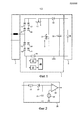
На фиг. 1 показан вариант осуществления схемы 1 возбуждения. Схема 1 возбуждения выполнена с возможностью подключения электромагнитного балласта 2, например пассивного балласта, который содержит, например, последовательный дроссель, к осветительной схеме 3, которая содержит один или более светодиодов. Схема 1 возбуждения содержит мостовой выпрямитель 11-14, имеющий вход для обмена первым сигналом тока с электромагнитным балластом 2 и выход для подачи второго сигнала тока на осветительную схему 3. Схема 1 возбуждения дополнительно содержит защитную схему 21-24, 25-27 для защиты электромагнитного балласта 2 от получения параметром первого сигнала тока значения, превышающего пороговое значение.In FIG. 1 shows an embodiment of an
Таким образом, первый входной разъем схемы 1 возбуждения подключен к первому выходному разъему электромагнитного балласта 2, причем первый выходной разъем подключен, например, к последовательному дросселю. Первый входной разъем схемы 1 возбуждения подключен к первому последовательному соединению двух диодных элементов 21 и 11 (его аноду), и к третьему последовательному соединению двух диодных элементов 23 и 13 (его катоду). Второй входной разъем схемы 1 возбуждения подключен ко второму выходному разъему электромагнитного балласта 2. Второй входной разъем схемы 1 возбуждения подключен ко второму последовательному соединению двух диодных элементов 22 и 12 (его аноду), и к четвертому последовательному соединению двух диодных элементов 24 и 14 (его катоду).Thus, the first input connector of the
Диодные элементы 11 и 12 (их катоды) подключены друг к другу и к первому главному контакту переключателя 27, в данном случае, к первому главному электроду транзистора. Диодные элементы 13 и 14 (их аноды) подключены друг к другу и к первой стороне резистора 29 и к входам детектора 25 среднего значения и детектора 26 пикового значения. Другая сторона резистора 29 подключена к земле. Выходы детекторов 25 и 26 подключены к входам объединительной схемы 28, например, вентиля ИЛИ, который выдает сигнал управления на управляющий контакт переключателя 27, в данном случае управляющий электрод транзистора. Второй главный контакт переключателя 27, в данном случае, второй главный электрод транзистора, подключен к аноду диода 32 и к первому главному контакту дополнительного переключателя 31, в данном случае, первому главному электроду дополнительного транзистора. Второй главный контакт дополнительного переключателя 31, в данном случае, второй главный электрод дополнительного транзистора, подключен к земле. Катод диода 32 образует первый выходной разъем схемы 1 возбуждения и подключен к одной стороне конденсатора 33 и к первому входному разъему осветительной схемы 3. Другая сторона конденсатора 33 образует второй выходной разъем схемы 1 возбуждения и подключен к земле и ко второму входному разъему осветительной схемы 3.The
В первом случае, когда требуется защита от получения параметром в форме составляющей постоянного тока первого сигнала тока значения, превышающего пороговое значение, в схеме 1 возбуждения диодные элементы 11-14 и 21-24 присутствуют, и все остальные элементы 25-29 можно опустить. В случае, когда один из диодных элементов 11-14 обладает слишком низким значением импеданса в своем запирающем направлении (стал так называемым короткозамыкателем), другой из диодных элементов 21-24 в том же последовательном соединении будет сохранять свою нормальную импедансную характеристику, и, в результате, комбинация мостового выпрямителя 11-14 и защитной схемы 21-24 сохраняет свою выпрямительную функцию. При этом первый и/или второй сигнал тока приобретет слегка асимметричную форму, и, в результате, составляющая постоянного тока или DC-составляющая в этом сигнале тока приобретет значение, чуть большее нуля, но это значение все еще будет не настолько велико, чтобы вызвать повреждение электромагнитного балласта 2.In the first case, when protection is required from a parameter in the form of a DC component of the first current signal receiving a value that exceeds a threshold value, diode elements 11-14 and 21-24 are present in the
DC-составляющая в сигнале тока будет, например, в сто раз меньше в случае, когда один из восьми диодных элементов становится короткозамыкателем, по сравнению со случаем, когда один из четырех диодных элементов становится короткозамыкателем в традиционной выпрямительной схеме.The DC component in the current signal will, for example, be one hundred times smaller in the case when one of the eight diode elements becomes a short-circuit, compared with the case when one of the four diode elements becomes a short-circuit in a traditional rectifier circuit.
Во втором случае, когда требуется защита от получения параметром в форме среднего значения выпрямленной версии первого сигнала тока значения, превышающего пороговое значение, в схеме 1 возбуждения диодные элементы 11-14 (или 21-24) присутствуют, и детектор 25 среднего значения, переключатель 27 и, например, резистор 29 присутствуют. На резисторе 29 присутствует сигнал напряжения, который позволяет детектору 25 среднего значения осуществлять детектирование, но специалист в данной области техники может предложить многочисленные другие альтернативы такому резистору. Так, в этом случае, защитная схема 25, 27 содержит детектор 25 для детектирования среднего значения второго сигнала тока, и это детектирование является альтернативой детектированию среднего значения выпрямленной версии первого сигнала тока, и содержит переключатель 27 для прерывания второго сигнала тока в соответствии с результатом детектирования.In the second case, when protection is required from the parameter in the form of the average value of the rectified version of the first current signal receiving a value that exceeds the threshold value, in the
В третьем случае, когда требуется защита от получения параметром в форме пикового значения первого сигнала тока значения, превышающего пороговое значение, в схеме 1 возбуждения диодные элементы 11-14 (или 21-24) присутствуют, и детектор 26 пикового значения, переключатель 27 и, например, резистор 29 присутствуют. На резисторе 29 присутствует сигнал напряжения, который позволяет детектору 26 пикового значения осуществлять детектирование, но специалист в данной области техники может предложить многочисленные другие альтернативы такому резистору. Так, в этом случае, защитная схема 26, 27 содержит детектор 26 для детектирования пикового значения второго сигнала тока, и это детектирование является альтернативой детектированию пикового значения первого сигнала тока, и содержит переключатель 27 для прерывания второго сигнала тока в соответствии с результатом детектирования.In the third case, when protection against receiving a parameter in the form of a peak value of the first current signal of a value exceeding the threshold value is required, in the
Пиковое значение сигнала тока становится чрезмерно высоким в случае, когда один из диодных элементов имеет слишком высокое значение импеданса в своем проводящем направлении (становится так называемым разрывом).The peak value of the current signal becomes excessively high when one of the diode elements has too high an impedance value in its conducting direction (becomes the so-called gap).
Дополнительный переключатель 31 позволяет управлять величиной мощности, подаваемой на осветительную схему 3. Таким образом, в непроводящем состоянии дополнительного переключателя 31, второй сигнал тока течет через диод 32 на осветительную схему 3 и также используется для зарядки конденсатора 33. В проводящем состоянии дополнительного переключателя 31, второй сигнал тока течет через этот дополнительный переключатель 31 на землю, и осветительная схема 3 получает свою мощность только от заряженного конденсатора 33. Диод 32 препятствует разряду этого конденсатора 33 через проводящий дополнительный переключатель 31. Специалист в данной области техники должен понимать, как управлять таким дополнительным переключателем 31. Альтернативно, некоторые или все из элементов 31-33 могут составлять часть осветительной схемы 3.An additional switch 31 allows you to control the amount of power supplied to the
В качестве альтернативы детектированию среднего значения выпрямленной версии первого сигнала тока или среднего значения второго сигнала тока, можно детектировать среднеквадратическое значение первого или второго сигнала тока. Однако среднеквадратические детекторы (в настоящее время) довольно сложны и довольно дороги. Детекторы среднего значения, например, RC-фильтры сравнительно просты и сравнительно дешевы.As an alternative to detecting the average value of the rectified version of the first current signal or the average value of the second current signal, the root mean square value of the first or second current signal can be detected. However, RMS detectors (currently) are quite complex and quite expensive. Medium detectors, such as RC filters, are relatively simple and relatively cheap.
На фиг. 2 показан вариант осуществления детектора 26 пикового значения. Детектор 26 содержит последовательно соединенные резистор 41, диод 42 и конденсатор 43, и дополнительно содержит компаратор 44 для сравнения амплитуды сигнала напряжения, присутствующего на конденсаторе 43, с пороговым значением напряжения, генерируемого источником 45, и для управления переключателем 27 в соответствии с результатом сравнения. Предпочтительно, комбинация значения сопротивления резистора 41 и значения емкости конденсатора 43 позволяет задавать время реакции детектора 26.In FIG. 2 shows an embodiment of a
Диодный элемент содержит диод, или стабилитрон, или транзистор, или его часть. Каждый из двух или более последовательно соединенных диодных элементов может содержать диод, или стабилитрон, или транзистор, или его часть. Каждый переключатель 27, 31 может представлять собой транзистор или переключатель любого другого рода. Детекторы 25 и 26 можно объединять, возможно, с помощью объединительной схемы 28. В случае использования только одного детектора 25, 26, объединительная схема 28 не нужна. Специалист в данной области техники может предложить многочисленные альтернативы объединительной схемы и многочисленные варианты осуществления для детекторов 25 и 26.The diode element contains a diode, or a zener diode, or a transistor, or part thereof. Each of two or more series-connected diode elements may contain a diode, or a zener diode, or a transistor, or a part thereof. Each
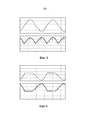
На фиг. 3 показаны формы волны для нормального состояния. Верхний график: первый сигнал тока. Нижний график: второй сигнал тока. По вертикальной оси отложен ток от -1 до 1 А. По горизонтальной оси отложено время от 0 до 33,3 мс.In FIG. 3 shows waveforms for a normal state. Upper graph: first current signal. Bottom graph: second current signal. A current from -1 to 1 A is plotted along the vertical axis. A time from 0 to 33.3 ms is plotted along the horizontal axis.
На фиг. 4 показаны формы волны для состояния отказа (один диодный элемент стал разрывом - детектор 26 пикового значения управляет переключатель 27 для прерывания второго сигнала тока). Верхний график: первый сигнал тока. Нижний график: второй сигнал тока. По вертикальной оси отложен ток от -1 до 1 А. По горизонтальной оси отложено время от 0 до 33,3 мс.In FIG. Figure 4 shows the waveforms for the failure state (one diode element became a gap - the
В итоге, для защиты электромагнитных балластов 2 от повреждения, схемы 1 возбуждения для подключения электромагнитных балластов 2 к осветительным схемам 3, содержащим светодиоды, снабжены мостовыми выпрямителями 11-14 для обмена первыми сигналами тока с электромагнитными балластами 2 и для подачи вторых сигналов тока на осветительные схемы 3, и защитными схемами 21-24, 25-27 для защиты электромагнитных балластов 3 от получения параметрами первых сигналов тока значений, превышающих пороговые значения. Параметры могут представлять собой составляющие постоянного тока первых сигналов тока и могут представлять собой средние значения выпрямленных версий первых сигналов тока/пиковые значения первых сигналов тока. Мостовые выпрямители 11-14 могут содержать первые диодные элементы. Защитные схемы 21-24, 25-27 могут содержать вторые диодные элементы, последовательно подключенные к первым диодным элементам. Защитная схема может содержать детекторы 25 среднего значения/детекторы 26 пикового значения, и может содержать переключатели 27 для прерывания вторых сигналов тока в соответствии с результатами детектирования.As a result, to protect
Хотя изобретение проиллюстрировано и подробно описано в чертежах и вышеприведенном описании, такие иллюстрация и описание следует рассматривать в порядке иллюстрации или примера, но не ограничения; изобретение не ограничивается раскрытыми вариантами осуществления. Специалисты в данной области техники могут понять и осуществить при практической реализации заявленного изобретения другие разновидности раскрытых вариантов осуществления, изучив чертежи, раскрытие и зависимые пункты формулы изобретения. В формуле изобретения, слово "содержащий" не исключает наличия других элементов или этапов, и употребление их наименований в единственном числе не исключает наличия их множества. Лишь тот факт, что определенные меры упомянуты во взаимно различных зависимых пунктах, не говорит о том, что нельзя выгодно использовать комбинацию этих мер. Никакие ссылочные позиции в нижеследующей формуле изобретения не следует рассматривать в порядке ограничения ее объема.Although the invention is illustrated and described in detail in the drawings and the above description, such illustration and description should be considered by way of illustration or example, but not limitation; the invention is not limited to the disclosed embodiments. Specialists in the art can understand and implement in the practical implementation of the claimed invention other varieties of the disclosed embodiments by studying the drawings, disclosure and dependent claims. In the claims, the word “comprising” does not exclude the presence of other elements or steps, and the use of their names in the singular does not exclude the presence of many of them. The mere fact that certain measures are mentioned in mutually different dependent clauses does not mean that a combination of these measures cannot be used to advantage. No reference position in the following claims should not be construed in order to limit its scope.
Claims (15)
Applications Claiming Priority (3)
| Application Number | Priority Date | Filing Date | Title |
|---|---|---|---|
| US201261664817P | 2012-06-27 | 2012-06-27 | |
| US61/664,817 | 2012-06-27 | ||
| PCT/IB2013/055236 WO2014002021A1 (en) | 2012-06-27 | 2013-06-26 | Driver circuit between electromagnetic ballast and led |
Publications (2)
| Publication Number | Publication Date |
|---|---|
| RU2015102286A RU2015102286A (en) | 2016-08-20 |
| RU2661891C2 true RU2661891C2 (en) | 2018-07-20 |
Family
ID=49165794
Family Applications (1)
| Application Number | Title | Priority Date | Filing Date |
|---|---|---|---|
| RU2015102286A RU2661891C2 (en) | 2012-06-27 | 2013-06-26 | Driver circuit between electromagnetic ballast and light-emitting diode |
Country Status (8)
| Country | Link |
|---|---|
| US (1) | US9426861B2 (en) |
| EP (1) | EP2868163B1 (en) |
| JP (1) | JP6346176B2 (en) |
| CN (1) | CN104429160B (en) |
| BR (1) | BR112014032079A2 (en) |
| PL (1) | PL2868163T3 (en) |
| RU (1) | RU2661891C2 (en) |
| WO (1) | WO2014002021A1 (en) |
Families Citing this family (7)
| Publication number | Priority date | Publication date | Assignee | Title |
|---|---|---|---|---|
| KR101247208B1 (en) * | 2012-08-07 | 2013-03-26 | 엠티엔시 (주) | Earth leakage breaker |
| CN103929858B (en) * | 2014-04-15 | 2015-11-25 | 刘坚 | The LED fluorescent lamp tube utilizing electronic ballast for fluoresent lamp to drive and lighting |
| EP3257329B1 (en) | 2015-02-13 | 2020-01-01 | Signify Holding B.V. | Device fed via ballast for producing light |
| US10305279B2 (en) | 2015-05-21 | 2019-05-28 | Lutron Technology Company Llc | Load control device having a reduced leakage through ground |
| CN106612129B (en) * | 2015-10-22 | 2022-11-15 | 从兴技术有限公司 | Low-voltage direct-current carrier circuit |
| CN107567150B (en) * | 2017-10-10 | 2019-06-14 | 矽力杰半导体技术(杭州)有限公司 | Input power sense circuit and detection method and the LED drive circuit comprising it |
| CN113170558B (en) * | 2018-12-04 | 2024-03-22 | 昕诺飞控股有限公司 | Retrofit lamp, lighting system using the same and protection method |
Citations (5)
| Publication number | Priority date | Publication date | Assignee | Title |
|---|---|---|---|---|
| US20040004446A1 (en) * | 2002-07-05 | 2004-01-08 | Hun-Huang Liu | Drive circuit for an led lighting apparatus |
| WO2006102355A2 (en) * | 2005-03-22 | 2006-09-28 | Fairchild Semiconductor Corporation | Single-stage digital power converter for driving leds |
| US20070267981A1 (en) * | 2006-05-16 | 2007-11-22 | Junzhong Peng | Power-Saving and Stabilizing Ballast |
| US20100033095A1 (en) * | 2008-02-08 | 2010-02-11 | Innosys, Inc. | Solid State Semiconductor LED Replacement for Fluorescent Lamps |
| WO2011155712A2 (en) * | 2010-06-08 | 2011-12-15 | 박성진 | Electronic ballast-type led fluorescent lamp |
Family Cites Families (5)
| Publication number | Priority date | Publication date | Assignee | Title |
|---|---|---|---|---|
| US7507001B2 (en) * | 2002-11-19 | 2009-03-24 | Denovo Lighting, Llc | Retrofit LED lamp for fluorescent fixtures without ballast |
| US7102297B2 (en) * | 2005-03-31 | 2006-09-05 | Osram Sylvania, Inc. | Ballast with end-of-lamp-life protection circuit |
| US20080290814A1 (en) * | 2006-02-07 | 2008-11-27 | Leong Susan J | Power Controls for Tube Mounted Leds With Ballast |
| JP2009026544A (en) * | 2007-07-18 | 2009-02-05 | Showa Denko Kk | Light-control device for light-emitting diode and led lighting device |
| CN103181241B (en) * | 2010-10-19 | 2016-06-08 | 皇家飞利浦电子股份有限公司 | The method of LED retrofit lamp, illuminator and operation LED retrofit lamp |
-
2013
- 2013-06-26 PL PL13762232T patent/PL2868163T3/en unknown
- 2013-06-26 CN CN201380034179.6A patent/CN104429160B/en active Active
- 2013-06-26 US US14/409,105 patent/US9426861B2/en active Active
- 2013-06-26 BR BR112014032079A patent/BR112014032079A2/en not_active Application Discontinuation
- 2013-06-26 RU RU2015102286A patent/RU2661891C2/en not_active Application Discontinuation
- 2013-06-26 WO PCT/IB2013/055236 patent/WO2014002021A1/en active Application Filing
- 2013-06-26 EP EP13762232.0A patent/EP2868163B1/en active Active
- 2013-06-26 JP JP2015519440A patent/JP6346176B2/en active Active
Patent Citations (5)
| Publication number | Priority date | Publication date | Assignee | Title |
|---|---|---|---|---|
| US20040004446A1 (en) * | 2002-07-05 | 2004-01-08 | Hun-Huang Liu | Drive circuit for an led lighting apparatus |
| WO2006102355A2 (en) * | 2005-03-22 | 2006-09-28 | Fairchild Semiconductor Corporation | Single-stage digital power converter for driving leds |
| US20070267981A1 (en) * | 2006-05-16 | 2007-11-22 | Junzhong Peng | Power-Saving and Stabilizing Ballast |
| US20100033095A1 (en) * | 2008-02-08 | 2010-02-11 | Innosys, Inc. | Solid State Semiconductor LED Replacement for Fluorescent Lamps |
| WO2011155712A2 (en) * | 2010-06-08 | 2011-12-15 | 박성진 | Electronic ballast-type led fluorescent lamp |
Also Published As
| Publication number | Publication date |
|---|---|
| BR112014032079A2 (en) | 2017-06-27 |
| CN104429160B (en) | 2017-08-25 |
| RU2015102286A (en) | 2016-08-20 |
| US20150195886A1 (en) | 2015-07-09 |
| EP2868163A1 (en) | 2015-05-06 |
| JP2015525949A (en) | 2015-09-07 |
| EP2868163B1 (en) | 2020-05-06 |
| PL2868163T3 (en) | 2020-11-16 |
| WO2014002021A1 (en) | 2014-01-03 |
| JP6346176B2 (en) | 2018-06-20 |
| CN104429160A (en) | 2015-03-18 |
| US9426861B2 (en) | 2016-08-23 |
Similar Documents
| Publication | Publication Date | Title |
|---|---|---|
| RU2661891C2 (en) | Driver circuit between electromagnetic ballast and light-emitting diode | |
| US10091858B2 (en) | Retrofit light emitting diode tube | |
| US9433055B2 (en) | Lighting device and illumination apparatus including same | |
| US8779679B2 (en) | LED lamp, illumination device including the LED lamp and current control method of the LED lamp | |
| RU2609130C2 (en) | Driver for connecting light-emitting diode to electronic ballast | |
| CN105979661A (en) | Time delay illumination circuit and device | |
| KR20150013314A (en) | Method, apparatus and system for controlling an electrical load | |
| JP2015156382A (en) | Led illumination | |
| CN102801308A (en) | Power supply device and lamp and vehicle including same | |
| US11770886B2 (en) | LED driving circuit, light tube and illumination device | |
| JP2017513184A (en) | Fluorescent lamp compatible type LED lighting device and electric shock protection device therefor | |
| CN109196953B (en) | Method of lighting driver protection and lighting driver comprising such protection | |
| WO2018024035A1 (en) | Indicating circuit for switching power supply, and using method therefor | |
| CN102622968A (en) | Multi-tube driving system | |
| JP2015158983A (en) | Lighting device and illuminating fixture | |
| US9480126B1 (en) | Method to detect uneven AC load or parallel load removal | |
| JP5785673B2 (en) | Output circuit for magnetic / electronic transformer |
Legal Events
| Date | Code | Title | Description |
|---|---|---|---|
| HZ9A | Changing address for correspondence with an applicant | ||
| FA92 | Acknowledgement of application withdrawn (lack of supplementary materials submitted) |
Effective date: 20180326 |
|
| FZ9A | Application not withdrawn (correction of the notice of withdrawal) |
Effective date: 20180326 |