RU2490615C2 - Multilayer arrays of colour sensors - Google Patents
Multilayer arrays of colour sensors Download PDFInfo
- Publication number
- RU2490615C2 RU2490615C2 RU2011148028/28A RU2011148028A RU2490615C2 RU 2490615 C2 RU2490615 C2 RU 2490615C2 RU 2011148028/28 A RU2011148028/28 A RU 2011148028/28A RU 2011148028 A RU2011148028 A RU 2011148028A RU 2490615 C2 RU2490615 C2 RU 2490615C2
- Authority
- RU
- Russia
- Prior art keywords
- analyte
- sublayer
- sensitive
- appearance
- thickness
- Prior art date
Links
Images


Classifications
-
- G—PHYSICS
- G01—MEASURING; TESTING
- G01N—INVESTIGATING OR ANALYSING MATERIALS BY DETERMINING THEIR CHEMICAL OR PHYSICAL PROPERTIES
- G01N21/00—Investigating or analysing materials by the use of optical means, i.e. using sub-millimetre waves, infrared, visible or ultraviolet light
- G01N21/75—Systems in which material is subjected to a chemical reaction, the progress or the result of the reaction being investigated
- G01N21/77—Systems in which material is subjected to a chemical reaction, the progress or the result of the reaction being investigated by observing the effect on a chemical indicator
- G01N21/78—Systems in which material is subjected to a chemical reaction, the progress or the result of the reaction being investigated by observing the effect on a chemical indicator producing a change of colour
-
- G—PHYSICS
- G01—MEASURING; TESTING
- G01N—INVESTIGATING OR ANALYSING MATERIALS BY DETERMINING THEIR CHEMICAL OR PHYSICAL PROPERTIES
- G01N21/00—Investigating or analysing materials by the use of optical means, i.e. using sub-millimetre waves, infrared, visible or ultraviolet light
- G01N21/17—Systems in which incident light is modified in accordance with the properties of the material investigated
- G01N21/25—Colour; Spectral properties, i.e. comparison of effect of material on the light at two or more different wavelengths or wavelength bands
-
- G—PHYSICS
- G01—MEASURING; TESTING
- G01N—INVESTIGATING OR ANALYSING MATERIALS BY DETERMINING THEIR CHEMICAL OR PHYSICAL PROPERTIES
- G01N31/00—Investigating or analysing non-biological materials by the use of the chemical methods specified in the subgroup; Apparatus specially adapted for such methods
- G01N31/22—Investigating or analysing non-biological materials by the use of the chemical methods specified in the subgroup; Apparatus specially adapted for such methods using chemical indicators
-
- G—PHYSICS
- G01—MEASURING; TESTING
- G01N—INVESTIGATING OR ANALYSING MATERIALS BY DETERMINING THEIR CHEMICAL OR PHYSICAL PROPERTIES
- G01N21/00—Investigating or analysing materials by the use of optical means, i.e. using sub-millimetre waves, infrared, visible or ultraviolet light
- G01N21/75—Systems in which material is subjected to a chemical reaction, the progress or the result of the reaction being investigated
- G01N21/77—Systems in which material is subjected to a chemical reaction, the progress or the result of the reaction being investigated by observing the effect on a chemical indicator
- G01N21/7703—Systems in which material is subjected to a chemical reaction, the progress or the result of the reaction being investigated by observing the effect on a chemical indicator using reagent-clad optical fibres or optical waveguides
- G01N2021/7706—Reagent provision
- G01N2021/7723—Swelling part, also for adsorption sensor, i.e. without chemical reaction
-
- G—PHYSICS
- G01—MEASURING; TESTING
- G01N—INVESTIGATING OR ANALYSING MATERIALS BY DETERMINING THEIR CHEMICAL OR PHYSICAL PROPERTIES
- G01N21/00—Investigating or analysing materials by the use of optical means, i.e. using sub-millimetre waves, infrared, visible or ultraviolet light
- G01N21/17—Systems in which incident light is modified in accordance with the properties of the material investigated
- G01N21/41—Refractivity; Phase-affecting properties, e.g. optical path length
- G01N21/45—Refractivity; Phase-affecting properties, e.g. optical path length using interferometric methods; using Schlieren methods
Landscapes
- Life Sciences & Earth Sciences (AREA)
- Physics & Mathematics (AREA)
- Chemical & Material Sciences (AREA)
- Health & Medical Sciences (AREA)
- General Physics & Mathematics (AREA)
- Pathology (AREA)
- Biochemistry (AREA)
- General Health & Medical Sciences (AREA)
- Analytical Chemistry (AREA)
- Immunology (AREA)
- Chemical Kinetics & Catalysis (AREA)
- Biophysics (AREA)
- Molecular Biology (AREA)
- Engineering & Computer Science (AREA)
- Plasma & Fusion (AREA)
- Spectroscopy & Molecular Physics (AREA)
- Investigating Or Analysing Materials By Optical Means (AREA)
- Investigating Or Analysing Materials By The Use Of Chemical Reactions (AREA)
Abstract
Description
Уровень техникиState of the art
Обнаружение определяемых при анализе веществ (аналитов), например, органических химических веществ, является важным компонентом во многих приложениях, например, при мониторинге состояния окружающей среды и ему подобных. Обнаружение и/или мониторинг аналитов может проводиться, например, приборами индивидуального пользования (переносными или носимыми на теле или одежде), и/или зональными приборами (которые, например, могут быть установлены в исследуемом окружении).The detection of substances (analytes) defined in the analysis, for example, organic chemicals, is an important component in many applications, for example, when monitoring the state of the environment and the like. Detection and / or monitoring of analytes can be carried out, for example, by devices for personal use (portable or worn on the body or clothes), and / or zonal devices (which, for example, can be installed in the studied environment).
Разработано множество способов обнаружения химических аналитов, включая оптические, гравиметрические, микроэлектромеханические и колориметрические способы. И хотя в настоящее время разработаны колориметрические приборы для широкого спектра аналитов, большинство из них основано на использовании красителей или окрашенных химических веществ-индикаторов. Такие вещества, как правило, являются высоко специфичными, что означает, что для обнаружения различных классов соединений необходимо иметь большой набор датчиков. Более того, большинство таких систем имеет ограниченный срок эксплуатации из-за эффекта фотоотбеливания или побочных химических реакций. Большинство таких систем требует также использования сложного и громоздкого оптико-электронного оборудования для считывания оптических показаний таких датчиков.Many methods have been developed for detecting chemical analytes, including optical, gravimetric, microelectromechanical, and colorimetric methods. Although colorimetric instruments have been developed for a wide range of analytes, most of them are based on the use of dyes or colored indicator chemicals. Such substances, as a rule, are highly specific, which means that for the detection of various classes of compounds it is necessary to have a large set of sensors. Moreover, most of these systems have a limited life due to the effect of photobleaching or adverse chemical reactions. Most of these systems also require the use of complex and bulky optoelectronic equipment to read the optical readings of such sensors.
Сущность изобретенияSUMMARY OF THE INVENTION
В настоящем изобретении предлагаются способы и устройства для обнаружения присутствия определяемого вещества (аналита). Такие способы и устройства могут содержать матрицу, содержащую по меньшей мере два чувствительных элемента, по-разному реагирующих на присутствие исследуемого аналита. Каждый из упомянутых чувствительных элементов содержит по меньшей мере один оптически реагирующий слой, содержащий по меньшей мере один высоко чувствительный к данному аналиту подслой. По меньшей мере один чувствительный элемент матрицы дополнительно содержит минимально чувствительный к данному аналиту подслой, составляющий часть толщины оптически реагирующего слоя.The present invention provides methods and devices for detecting the presence of a detectable substance (analyte). Such methods and devices may contain a matrix containing at least two sensing elements that respond differently to the presence of the analyte under study. Each of these sensitive elements contains at least one optically reactive layer containing at least one sublayer highly sensitive to this analyte. At least one sensor element of the matrix further comprises a sublayer that is minimally sensitive to a given analyte, which is part of the thickness of the optically reactive layer.
В одном из воплощений изобретения предлагается матрица для оптического обнаружения аналита, содержащая по меньшей мере два отдельно считываемых чувствительных элемента, причем каждый из упомянутых чувствительных элементов содержит оптически реагирующий слой, расположенный между двумя отражающими слоями, причем оптически реагирующий слой каждого из чувствительных элементов содержит по меньшей мере высоко чувствительный к аналиту первый подслой, и причем оптически реагирующий слой по меньшей мере одного из чувствительных элементов дополнительно содержит минимально чувствительный к аналиту второй подслой, причем первый подслой и второй подслой каждого из чувствительных элементов имеют толщину, и причем толщина первого подслоя и второго подслоя одного чувствительного элемента значительного отличаются от толщины соответственно первого и второго подслоя другого чувствительного элемента.In one embodiment of the invention, there is provided an optical analyte detection matrix comprising at least two separately readable sensing elements, each of said sensing elements comprising an optically reactive layer located between two reflective layers, the optically reacting layer of each of the sensitive elements comprising at least the first sublayer is at least highly sensitive to analyte, and wherein the optically reactive layer of at least one of the sensitive elements additionally contains a second sublayer that is minimally sensitive to analyte, the first sublayer and the second sublayer of each of the sensitive elements have a thickness, and the thickness of the first sublayer and the second sublayer of one sensitive element differ significantly from the thickness of the first and second sublayer of the other sensitive element, respectively.
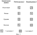
Во втором воплощении изобретения предлагается оптический способ обнаружения аналита в исследуемой атмосфере, содержащий этапы: обеспечения матрицы, содержащей по меньшей мере первый чувствительный элемент, изменяющий внешний вид от первого внешнего вида на второй внешний вид при первой, низкой концентрации аналита в исследуемой атмосфере, и изменяющий внешний вид от второго внешнего вида обратно на первый внешний вид при второй, высокой концентрации аналита; и по меньшей мере второй чувствительный элемент, который при первой, низкой концентрации аналита не меняет внешнего вида с первого внешнего вида на второй внешний вид, при третьей, промежуточной концентрации (большей первой концентрации и меньшей второй концентрации) меняет внешний вид с первого внешнего вида на второй внешний вид; а при второй, высокой концентрации не меняет внешнего вида со второго внешнего вида обратно на первый внешний вид; и воздействия на матрицу из чувствительных элементов атмосферы, потенциально содержащей данный аналит.In a second embodiment of the invention, there is provided an optical method for detecting analyte in a test atmosphere, comprising the steps of: providing a matrix comprising at least a first sensing element, changing the appearance from the first appearance to the second appearance at the first, low analyte concentration in the studied atmosphere, and changing appearance from the second appearance back to the first appearance with a second, high analyte concentration; and at least a second sensitive element, which at the first, low analyte concentration does not change the appearance from the first appearance to the second appearance, at the third, intermediate concentration (greater than the first concentration and lower second concentration) changes the appearance from the first appearance to second appearance; and in the second, high concentration does not change the appearance from the second appearance back to the first appearance; and effects on the matrix of sensitive elements of the atmosphere, potentially containing the analyte.
Данные, а также прочие воплощения изобретения будут более ясны из приведенного ниже подробного описания изобретения. Кроме того, приведенные выше краткие описания воплощений изобретения ни в коей мере не следует рассматривать как ограничения предмета изобретения, так как предмет изобретения определяется исключительно прилагаемой формулой изобретения, которая может быть скорректирована в процессе рассмотрения заявки.Data, as well as other embodiments of the invention, will be more apparent from the following detailed description of the invention. In addition, the above brief descriptions of embodiments of the invention should in no way be construed as limiting the subject of the invention, since the subject of the invention is determined solely by the attached claims, which may be adjusted during the consideration of the application.
Краткое описание чертежейBrief Description of the Drawings
Фиг.1. Сечение фрагмента одного из возможных воплощений чувствительного элемента.Figure 1. A section of a fragment of one of the possible embodiments of the sensing element.
Фиг.2. Примерный вид спектра отражения чувствительного элемента в соответствии с воплощениями настоящего изобретения.Figure 2. An exemplary view of the reflection spectrum of a sensor in accordance with embodiments of the present invention.
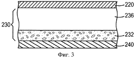
Фиг.3. Сечение фрагмента чувствительного элемента в соответствии с еще одним воплощением изобретения.Figure 3. A cross-section of a fragment of a sensing element in accordance with another embodiment of the invention.
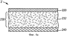
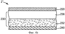
Фиг.4a, 4b и 4c. Сечение фрагмента чувствительного элемента в соответствии с различными воплощениями изобретения.Figa, 4b and 4c. A cross-section of a fragment of a sensing element in accordance with various embodiments of the invention.
Фиг.5. Схематическое отображение реакции матрицы из двух чувствительных элементов на различные концентрации аналита в исследуемой атмосфере.Figure 5. Schematic representation of the reaction of a matrix of two sensitive elements to various analyte concentrations in the atmosphere under study.
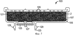
Фиг.6. Аксонометрический вид респиратора со сменными картриджами с сорбентом, содержащего матрицу из чувствительных элементов.6. Axonometric view of a respirator with replaceable cartridges with a sorbent containing a matrix of sensitive elements.
Фиг.7. Сечение сменного картриджа, используемого в респираторе, изображенном на фиг.6.7. The cross-section of a replaceable cartridge used in the respirator shown in Fig.6.
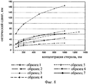
Фиг.8. График полученной на основании экспериментальных данных зависимости наблюдаемого оптического сдвига различных чувствительных элементов, находящихся под воздействием различных концентраций исследуемого аналита.Fig. 8. A graph of the dependence of the observed optical shift of various sensitive elements under the influence of different concentrations of the analyte studied, obtained on the basis of experimental data.
Аналогичные номера позиций на чертежах обозначают аналогичные элементы. Если явно не указано иное, все чертежи в настоящей заявке не обязательно выполнены в масштабе, и приводятся с целью иллюстрации различных воплощений изобретения. В частности, размеры различных компонентов на чертежах являются только лишь иллюстративными, и никаких выводов о пропорциях размеров различных компонентов из данных чертежей делать не следует. Несмотря на то, что в настоящей заявке могут использоваться такие термины, как «верх», «низ», «верхний», «нижний», «вверх», «вниз», «под», «над», «передний», «задний», «наружу», «вовнутрь», «первый» и «второй», следует понимать, что данные термины используются только в их относительном смысле, если явно не указано иное. В частности, такие характеристики, как «низкий», «средний» и «высокий», употребляемые в отношении определенных параметров (например, концентрации), следует понимать как относительные (сравнительные) в рамках данного контекста (так, например, «средней» считается концентрация между «низкой» и «высокой» в рамках одного и того же контекста).Similar item numbers in the drawings indicate like elements. Unless explicitly stated otherwise, all of the drawings in this application are not necessarily made to scale, and are provided to illustrate various embodiments of the invention. In particular, the dimensions of the various components in the drawings are merely illustrative, and no conclusions should be drawn about the proportions of sizes of the various components from these drawings. Although the terms “top”, “bottom”, “top”, “bottom”, “up”, “down”, “under”, “above”, “front”, can be used in this application “Back”, “out”, “in”, “first” and “second”, it should be understood that these terms are used only in their relative sense, unless explicitly stated otherwise. In particular, characteristics such as “low”, “medium” and “high”, used in relation to certain parameters (for example, concentration), should be understood as relative (comparative) in the context of this context (for example, “medium” is considered concentration between “low” and “high” within the same context).
Подробное описание изобретенияDETAILED DESCRIPTION OF THE INVENTION
В соответствии с одним из воплощений изобретения предлагается матрица 1, содержащая по меньшей мере первый чувствительный элемент 2' и второй чувствительный элемент 2'' (смотри, например, фиг.5 и 6). Каждый из чувствительных элементов содержит оптически реагирующий слой 230, который будет подробно описан ниже. Слой 230 во втором чувствительном элементе 2'' отличается от слоя 230 в первом чувствительном элементе 2' тем, что второй чувствительный элемент 2'' иным образом реагирует по меньшей мере на некоторую концентрацию исследуемого аналита. (В контексте настоящей заявки описания данное, а также прочие упоминания концентрации относятся к концентрации аналита в атмосфере, воздействию которой подвержены чувствительные элементы.)In accordance with one embodiment of the invention, there is provided a matrix 1 comprising at least a first sensor 2 'and a second sensor 2' '(see, for example, FIGS. 5 and 6). Each of the sensing elements comprises an optically
В частности, второй чувствительный элемент 2'' оптически не реагирует (например, в виде сдвига спектра отражения по меньшей мере на 15 нм, или в форме визуально заметного изменения; оба данных типа реагирования будут подробно описаны ниже) на определенную, низкую концентрацию аналита, на которую оптически реагирует первый чувствительный элемент 2', и в то же время второй чувствительный элемент 2'' оптически реагирует на иную, более высокую концентрацию аналита. За счет того, что первый чувствительный элемент 2' является чувствительным к низкой концентрации аналита, а второй чувствительный элемент 2'' является чувствительным к высокой концентрации аналита, матрица, содержащая по меньшей мере два таких чувствительных элемента, может оптически реагировать на более широкий диапазон концентраций аналита, чем это может делать единичный чувствительный элемент. В некоторых воплощениях матрица 1 содержит множество чувствительных элементов (например, три, четыре, пять, шесть или более), которые могут обеспечивать реагирование матрицы на еще более широкий диапазон концентраций аналита. Использование матриц в соответствии с настоящим изобретением может также обеспечивать и прочие дополнительные преимущества, которые будут более подробно описаны ниже.In particular, the
На фиг.1 изображен чувствительный элемент 2 (данного типа общее упоминание чувствительного элемента здесь и далее включает элементы 2', 2'' и прочие им подобные, упоминаемые в настоящем описании), в соответствии с одним из воплощений настоящего изобретения. Чувствительный элемент 2 представляет собой многослойную структуру, содержащую по меньшей мере оптически реагирующий слой 230, расположенный между отражающим слоем 240 и полу-отражающим слоем 220, так что упомянутые слои в сочетании образуют так называемый интерференционный фильтр, характеризующийся спектром отражения, который может меняться в присутствии аналита. Чувствительный слой 2 имеет спектр отражения, примерный вид которого изображен на фиг.2. Данный спектр содержит один или более пиков (например, пики 181, 183 и 184) и впадин (например, 185), соответствующие различным длинам волны отраженного света и которые могут меняться в присутствии аналита. Так, например, присутствие достаточного количества аналита может вызывать сдвиг пиков и впадин спектра отражения, изображенного на фиг.2, в сторону большей длины волны. Спектр отражения чувствительного элемента 2 может быть определен визуально, то есть по его внешнему виду (например, по относительно преобладающему цвету или оттенку), который может меняться в присутствии достаточного количества аналита. То есть, при воздействии на него достаточной концентрации аналита внешний вид чувствительного элемента 2 может меняться от первого (исходного внешнего вида) ко второму внешнему виду, визуально отличимому от первого внешнего вида.Figure 1 shows the sensor 2 (of this type, a common reference to the sensor hereinafter includes elements 2 ', 2' 'and the like, mentioned in the present description), in accordance with one embodiment of the present invention. The
Чувствительный элемент 2 может быть оптически считан при воздействии на него лучей 40 падающего света (как показано на фиг.1) и наблюдении за светом, отраженным от чувствительного элемента 2. Для обеспечения лучей 40 не требуется специального внешнего источника света (хотя при необходимости могут использоваться один или более специальных источников света). Лучи 40 света могут исходить из единственного дискретного источника света; или же в качестве источника лучей 40 света может использоваться внешнее освещение (которое в свою очередь может исходить от нескольких дискретных источников света, представлять собой сочетание света, исходящего непосредственно от источников света, и отраженного света, может быть солнечным светом и прочими видами освещения).The
В воплощениях, содержащих конструкцию, изображенную на фиг.1, чувствительный элемент 2 содержит (по порядку): основу 210 (дополнительно возможную), полу-отражающий слой 220, оптически реагирующий слой 230 и отражающий слой 240. Лучи 40 света падают на основу 210 и проходят через нее. Некоторая часть лучей 40 света может отражаться от полу-отражающего слоя 220 и выходить из чувствительного элемента 2 в виде лучей 41 света. Еще одна часть лучей 40 света может проходить через полу-отражающий слой 220 и далее через оптически реагирующий слой 230 к отражающему слою 240. По меньшей мере часть данных лучей может отразиться от отражающего слоя 240 и выйдет из чувствительного элемента 2 в виде лучей 42 света. Лучи 41 и 42 могут взаимодействовать (интерферировать конструктивно и/или деструктивно), в совокупности формируя спектр отражения чувствительного элемента, который может меняться в присутствии аналита или при изменении концентрации аналита.In embodiments containing the structure shown in FIG. 1, the
В конструкции, изображенной на фиг.1, аналит может проникать через отражающий слой 240 и попадать в оптически реагирующий слой 230. Это может приводить к изменению оптических свойств (например, оптической толщины по меньшей мере части слоя 230 (например, подслоя 230, как будет более подробно описано ниже), в результате чего спектральный состав света, отраженного от чувствительного элемента 2, может значительно меняться, что может позволить зафиксировать присутствие аналита и/или изменение его концентрации. В воплощениях, в которых используется конструкция, изображенная на фиг.1, отражающий слой 240 является проницаемым для аналита, и связан с оптически реагирующий слоем 230 по исследуемой среде. В конструкции, изображенной на фиг.1, полу-отражающий слой 220 может быть проницаемым или непроницаемым для аналита. В конструкции, изображенной на фиг.1, свет может беспрепятственно проходить через основу 210, то есть основа 210 может быть оптически прозрачной в соответствующем диапазоне длины волны.In the structure of FIG. 1, the analyte can penetrate through the
Возможны и прочие варианты конструкции. Так, например, проницаемым для аналита может быть полуотражающий слой 220, а не отражающий слой 240. Свойства оптически реагирующего слоя 230, основы 210 (если таковая имеется), полуотражающего слоя 22 и/или отражающего слоя 240, как будет более подробно описано ниже, подразумеваются как таковые, что из них в целом может быть изготовлен отражающий чувствительный элемент (работающий по принципу интерференции света). Сведущим в данной области техники будет понятно, что хотя на чертежах в различных чувствительных элементах матрицы могут использоваться одни и те же номера позиций для обозначения вышеупомянутых слоев, слои, обозначенные такими номерами позиций, могут иметь одинаковые или различные конфигурации и/или состав.Other design options are also possible. So, for example, the analyte can be permeable to the
Оптически реагирующий слой 230 определяется как слой, имеющий оптическую толщину (физическая толщина, умноженная на коэффициент преломления), по меньшей мере часть которой может меняться в присутствии аналита, в результате чего спектр отражения, определяемый сочетанием оптически реагирующего слоя 230, отражающего слоя 240 и полуотражающего слоя 220, может значительно сдвигаться (где под термином «значительно» понимается, что в обычных условиях эксплуатации чувствительного элемента 2 может быть зафиксировано изменение внешнего вида чувствительного элемента 2) при воздействии на чувствительный элемент 2 определенной концентрации аналита. В частности, оптически реагирующий слой 230, будучи расположен между подходящими отражающим слоем 240 и полу-отражающим слоем 220, может характеризоваться сдвигом спектра отражения по меньшей мере на 15 нм при воздействии на чувствительный элемент 2 атмосферы, содержащей 1000 ppm стирола как достаточно представительного типа исследуемого органического аналита. Здесь и далее все упоминания о сдвиге спектра относятся к результатам измерений в соответствии с процедурой измерений, описанной в разделе «Реакция образцов на тестовый аналит» ниже. Термин «оптически реагирующий», употребляемый в отношении слоя 230 дополнительно означает, что суммарная (физическая) толщина слоя 230, считая все его подслои в целом, по порядку величины равна длине волны видимого света или близка к ней (то есть составляет от примерно 100 нм до примерно 2000 нм). В различных воплощениях суммарная физическая толщина слоя 230 может составлять от примерно 200 нм до примерно 1500 нм, о примерно 400 нм до примерно 1000 нм, или от примерно 500 нм до примерно 800 нм (все вышеупомянутые значения толщины относятся к физической толщине, а не к оптической толщине, если явно не указано иное.)An optically
Оптически реагирующий слой 230 может содержать по меньшей мере два подслоя 232 и 236, как показано на фиг.3. Подслой 232 является высокочувствительным к аналиту подслоем (в контексте настоящего описания), а подслой 236 является подслоем, минимально чувствительным к аналиту подслоем (также в контексте настоящего описания). В различных воплощениях толщина высокочувствительного к аналиту подслоя 232 может составлять от примерно 100 нм до примерно 800 нм. Толщина минимально чувствительного к аналиту подслоя 236 в различных воплощениях может составлять от примерно 700 нм до примерно 0 нм (последнее означает, что в одном или более чувствительных элементах 2 матрицы 1 может вовсе отсутствовать минимально чувствительный к аналиту подслой 236). В различных воплощениях суммарная толщина подслоев 232 и 236 может составлять от примерно 200 нм до примерно 1500 нм. В некоторых воплощениях суммарная толщина подслоев 232 и 236 может составлять от примерно 400 нм до примерно 1000 нм, или от примерно 500 нм до примерно 800 нм.The optically
Итак, матрица 1 в соответствии с настоящим изобретением содержит по меньшей мере два чувствительных элемента 2, по меньшей мере два из которых: 2' и 2'' - содержат подслои 232, значительно различающиеся по толщине, и/или подслои 236, значительно различающиеся по толщине. В контексте настоящего описания разность толщины высокочувствительных к аналиту подслоев 232 первого и второго чувствительных элементов считается значительной, если она составляет по меньшей мере 20 нм. Так, например, для двух чувствительных элементов, в одном из которых подслой 232 имеет толщину 600 нм, а в другом из которых подслой 232 имеет толщину 580 нм, разность толщины подслоев считается значительной. Подобным образом, разность между толщиной минимально чувствительных к аналиту подслоев 236 двух чувствительных элементов считается значительной, если она также превышает 20 нм. Так, например, для двух чувствительных элементов, в одном из которых подслой 236 имеет толщину 130 нм, а в другом из которых подслой 236 имеет толщину 150 нм, разность толщины подслоев считается значительной. В различных воплощениях разность толщины соответствующих подслоев 236 двух чувствительных элементов 2 может составлять по меньшей мере примерно 50 нм, или по меньшей мере 100 нм.So, the matrix 1 in accordance with the present invention contains at least two
На фиг.4 представлены поперечные сечения трех возможных типов чувствительных элементов 2', 2'' и 2''', сочетание из двух или более из которых может использоваться в матрице 1. Каждый из чувствительных элементов содержит оптически реагирующий слой 230 примерно одинаковой физической толщины (в контексте настоящего описания одинаковой считается толщина в пределах ±15%), и примерно одинаковой оптической толщины в отсутствии аналита, так что каждый из данных элементов в отсутствии аналита имеет примерно одинаковый внешний вид. Оптически реагирующий слой 230 чувствительного элемента 2', изображенного на фиг.4a, содержит высоко чувствительный к аналиту подслой 232 и не содержит минимально чувствительного слоя 236. Оптически реагирующий слой воплощения чувствительного элемента 2'', изображенного на фиг.4b., содержит подслои 232 и 236 примерно одинаковой толщины. Оптически реагирующий слой воплощения чувствительного элемента 2''', изображенного на фиг.4c, содержит подслои 232 и 236, причем толщина подслоя 236 примерно вдвое больше толщины подслоя 232.4 shows cross sections of three possible types of sensors 2 ', 2' 'and 2' '', a combination of two or more of which can be used in matrix 1. Each of the sensors contains an optically
Подслой 232 является высокочувствительным по отношению к исследуемому аналиту, что достигается за счет выбора подходящих материалов, которые содержит подслой 232. В данном контексте «высоко чувствительный к аналиту» означает, что подслой 232 является достаточно проницаемым для аналита, и что присутствие аналита в слое 232 приводит к изменению оптической толщины подслоя 232, а следовательно, и оптической толщины всего слоя 230, достаточному для того, чтобы произошел заметный сдвиг спектра отражения чувствительного элемента 2. В частности, термин «высоко чувствительный к аналиту» означает, что подслой 232 изготовлен из материала, который, будучи помещен между подходящим отражающим слоем и полу-отражающим слоем в виде слоя толщиной 400-800 нм, имеет спектр отражения, который сдвинется по меньшей мере примерно на 15 нм под воздействием атмосферы, содержащей примерно 50 ppm стирола. (Как было указано выше, здесь, до этого и далее стирол упоминается как полезный представительный органический аналит, то есть как аналит, удобный для описания характеристик чувствительности материалов, используемых в настоящем изобретении. Упоминание в данном контексте стирола ни коим образом не следует рассматривать как ограничение настоящего изобретения приложениями, связанными с наблюдением за концентрацией стирола). В различных воплощениях высоко чувствительный к аналиту подслой 232 может быть изготовлен из материала, который, будучи помещен между подходящим отражающим слоем и полу-отражающим слоем в виде слоя толщиной 400-800 нм, имеет спектр отражения, который под воздействием атмосферы, содержащей примерно 50 ppm стирола, сдвинется по меньшей мере примерно на 25 нм, по меньшей мере примерно на 35 мм или по меньшей мере примерно на 45 нм.
Подслой 236 является минимально чувствительным к исследуемому аналиту, что достигается за счет выбора материалов, которые содержит подслой 236. В данном контексте «минимально чувствительный к аналиту» означает или что подслой 236 является достаточно непроницаемым по отношению к аналиту, и/или что присутствие аналита в слое 236 не приводит к изменению оптической толщины подслоя 236, которая проявилась бы в изменении оптических свойств слоя 230 в виде заметного сдвига спектра отражения чувствительного элемента 2. В частности, термин «минимально чувствительный к аналиту» означает, что подслой 236 изготовлен из материала, который, будучи помещен между подходящим отражающим слоем и полуотражающим слоем в виде слоя толщиной 400-800 нм, имеет спектр отражения, который под воздействием атмосферы, содержащей примерно 20 ppm стирола, сдвинется не более чем примерно на 10 нм. В различных воплощениях минимально чувствительный к аналиту подслой 236 изготовлен из материала, который, будучи помещен между подходящим отражающим слоем и полу-отражающим слоем в виде слоя толщиной 400-800 нм, имеет спектр отражения, который под воздействием атмосферы, содержащей примерно 20 ppm стирола, сдвинется не более чем примерно на 5 нм, не более чем примерно на 3 нм, не более чем примерно на 1 нм.
За счет использования в оптически реагирующем слое 230 подслоя 230, содержащего высоко чувствительный к аналиту материал, и подслоя 236, содержащего минимально чувствительный к аналиту материал, общей чувствительностью слоя 230 (а следовательно, и всего чувствительного элемента 2) к данному уровню концентрации аналита можно управлять, меняя вклад в слой 230 от каждого из подслоев. Так, например, чувствительный элемент, содержащий оптически реагирующий слой 230, содержащий минимально чувствительный к аналиту подслой 236, может требовать присутствия аналита в более высокой концентрации, чтобы произошел сдвиг спектра отражения, сравнимый со сдвигом спектра отражения элемента, содержащего оптически реагирующий слой 230 примерно такой же толщины, но не содержащего подслоя 236.Due to the use in the optically
Так, например, в одном из воплощений изобретения чувствительный элемент 2 может содержать оптически реагирующий слой 230, содержащий высоко чувствительный к аналиту подслой 232 и минимально чувствительный к аналиту подслой 236 в такой конфигурации, что (даже несмотря на то, что высоко чувствительный к аналиту подслой 232 может быть изготовлен из материала, который, будучи помещен между подходящим отражающим слоем и полу-отражающим слоем в виде слоя толщиной 400-800 нм, имеет спектр отражения, сдвигающийся, например, на 100 мм под воздействием атмосферы, содержащей 200 ppm стирола) сдвиг спектра отражения чувствительного элемента 2 под воздействием атмосферы, содержащей 200 ppm стирола, составит не более чем примерно 40 нм. В различных воплощениях чувствительный элемент 2 может содержать высоко чувствительный к аналиту слой 232 и минимально чувствительный к аналиту подслой 236 в такой конфигурации, что сдвиг спектра отражения чувствительного элемента 2 под воздействием атмосферы, содержащей 200 ppm стирола, составит не более чем примерно 30 нм, или не более чем примерно 20 нм.So, for example, in one embodiment of the invention, the
Матрица, содержащая множество отдельных чувствительных элементов 2, каждый из которых характеризуется различной толщиной подслоя 232 и/или подслоя 236, может таким образом быть «динамически» чувствительной к широкому диапазону концентраций аналита, что дает преимущества, которые будут подробно описаны ниже.A matrix containing a plurality of
Кроме того, путем выбора подходящей толщины минимально чувствительного к аналиту подслоя 236 в сочетании с подходящей толщиной высоко чувствительного к аналиту подслоя 232, что обеспечивает определенную суммарную толщину оптически реагирующего слоя 230, может быть получен исходный спектр отражения чувствительного элемента 2 (то есть его спектр отражения в отсутствии аналита или в присутствии аналита в необнаружимой концентрации), который может, например, придавать чувствительному элементу 2 определенный внешний вид при визуальном осмотре (например, определенный цвет). За счет такой конфигурации может быть изготовлен чувствительный элемент 2, содержащий подслои 232 и 236 и имеющий такой же внешний вид, который имел бы чувствительный элемент 2, содержащий только высоко чувствительный к аналиту материал (и не содержащий подслоя 236), и в то же время чувствительный к другой (более высокой) концентрации аналита, чем чувствительный элемент 2, содержащий только высоко чувствительный к аналиту материал. Таким образом, в матрице, содержащей множество отдельных чувствительных элементов 2, некоторые или все из упомянутых чувствительных элементов могут иметь практический одинаковый внешний вид, и тем не менее быть чувствительными к различным уровням концентрации аналита, что может обеспечивать преимущества, которые будут обсуждаться ниже.In addition, by choosing the appropriate thickness of the analyte-
Итак, использование оптически реагирующего слоя 230, содержащего подслои 232 и 236, позволяет получить чувствительный элемент 2, чувствительный к требуемому диапазону концентраций аналита, а также имеющий требуемый цвет или другой внешний признак.Thus, the use of an optically
Такое сочетание высоко чувствительного к аналиту подслоя 232 и минимально чувствительного к аналиту подслоя 236 может обеспечивать преимущества, важные по меньшей мере для некоторых приложений. В частности, сведущим в данной области техники известно, что отражательные датчики общего типа, используемые в настоящее время, могут быть подвержены явлению, именуемому «циклический переход». Циклический переход означает, что под воздействием достаточно высокой концентрации аналита спектр отражения датчика может меняться настолько, что датчик примет внешний вид, близкий к его исходному внешнему виду, который он имел в отсутствие аналита. (При воздействии еще более высоких концентраций аналита возможны и дальнейшие превращения внешнего вида датчика). К своему удивлению изобретатели обнаружили, что использование оптически реагирующего слоя 230, содержащего высоко чувствительный к аналиту подслой 232 в сочетании с минимально чувствительным к аналиту подслоем 236 позволяет получить чувствительный элемент 2, менее подверженный эффекту циклического перехода. В различных воплощениях свойства и толщина подслоев 232 и 236 могут быть подобраны таким образом, что чувствительный элемент 2 может не быть подверженным эффекту циклического перехода даже при чрезвычайно высоких концентрациях аналита. Так, например, различные воплощения чувствительного элемента 2 могут не иметь эффекта циклического перехода даже при концентрациях органического аналита, например, стирола, вплоть до 200, 400 или даже 1000 ppm.Such a combination of a highly analyte
В различных воплощениях изобретения такая способность не испытывать циклического перехода может быть обеспечена для чувствительных элементов, характеризующихся сдвигом спектра отражения, составляющим менее чем примерно 100 нм, менее чем примерно 80 нм или менее чем примерно 60 нм под воздействием атмосферы, содержащей 200 ppm органического аналита, например, стирола. В некоторых воплощениях изобретения такая способность не испытывать циклического перехода может быть обеспечена для чувствительных элементов, характеризующихся сдвигом спектра отражения, составляющим менее чем примерно 100 нм, менее чем примерно 80 нм или менее чем примерно 60 нм под воздействием атмосферы, содержащей 400 ppm органического аналита, например, стирола. В некоторых воплощениях изобретения такая способность не испытывать циклического перехода может быть обеспечена для чувствительных элементов, характеризующихся сдвигом спектра отражения, составляющим менее чем примерно 100 нм, менее чем примерно 80 нм или менее чем примерно 60 нм под воздействием атмосферы, содержащей 1000 ppm органического аналита, например, стирола. Таким образом может быть изготовлена матрица, в которой один или более чувствительных элементов 2 не будут подвержены эффекту циклического перехода даже в присутствии максимальных ожидаемых концентраций органического аналита. Такие устройства могут обеспечивать преимущества, которые будут описаны ниже.In various embodiments of the invention, this ability to not experience a cyclic transition can be provided for sensitive elements characterized by a shift in the reflection spectrum of less than about 100 nm, less than about 80 nm, or less than about 60 nm when exposed to an atmosphere containing 200 ppm organic analyte, for example styrene. In some embodiments of the invention, this ability to not experience a cyclic transition can be provided for sensitive elements characterized by a shift in the reflection spectrum of less than about 100 nm, less than about 80 nm, or less than about 60 nm when exposed to an atmosphere containing 400 ppm organic analyte, for example styrene. In some embodiments of the invention, this ability to not experience a cyclic transition can be provided for sensitive elements characterized by a shift in the reflection spectrum of less than about 100 nm, less than about 80 nm, or less than about 60 nm when exposed to an atmosphere containing 1000 ppm of organic analyte, for example styrene. In this way, a matrix can be made in which one or more of the
Высокочувствительный к аналиту подслой 232 может содержать любой материал, обладающий достаточно высокой чувствительностью к аналиту, по сравнению с минимально чувствительным к аналиту подслоем 236, в сочетании с которым он используется. Как было указано выше, подслой 232 является достаточно проницаемым по отношению к исследуемому аналиту и имеет оптическую толщину, которая под воздействием требуемой концентрации аналита может меняться в достаточной степени для функционирования чувствительного элемента 2 в смысле, описанном выше. И хотя теоретически это не обязательно, оптическая толщина подслоя 232 может меняться при его реакции на аналит, проникающий, например, за счет заполнения пор в материале, по меньшей мере частью которого является подслой 232, что может приводить к увеличению оптической толщины по меньшей мере за счет увеличения коэффициента преломления. Оптическая толщина подслоя 232 может также меняться при проникновении аналита в подслой и его набухании, то есть в данном случае оптическая толщина может увеличиваться по меньшей мере за счет увеличения физической толщины слоя. В некоторых материалах реакция на аналит может быть смешанной, то есть представлять собой сочетание упомянутых выше способов реакции на аналит. В некоторых материалах при некоторых концентрациях аналита может преобладать один из упомянутых выше типов реакции, а при других концентрациях - второй из упомянутых типов реакции; и так далее.The analyte-
В некоторых воплощениях подслой 232 содержит пористый материал. В данном контексте «пористый» означает, что материал содержит внутренние поры, которые по меньшей мере частично сообщаются между собой. Могут быть, например, выбраны материалы со средним размером пор (определяемым, например, методом изотермической сорбции) менее чем примерно 100 нм. В некоторых воплощениях могут быть, например, выбраны материалы со средним размером пор менее чем примерно 20 нм, менее чем примерно 10 нм или менее чем примерно 2 нм. Подслой 232 может быть гомогенным или гетерогенным и может быть, например, изготовлен из одного или более неорганических компонентов, одного или более органических компонентов, или из смеси органических и неорганических компонентов. Типичные неорганические материалы, которые могут быть использованы для изготовления подслоя 232, включают оксиды металлов, нитриды металлов, оксинитриды металлов и прочие неорганические материалы, из которых могут быть сформированы прозрачные (и при необходимости пористые слои) подходящей толщины, имеющие подходящую оптическую чувствительность.In some embodiments, the
Особенно подходящим неорганическим материалом, чувствительным к аналиту, может быть пористый кремнезем. Пористые кремнеземы могут быть, например, изготовлены путем обработки золево-гельных смесей с преобразованием их в силикат, содержащий сеть из пор в толще кремнезема. Для получения неорганических пористых материалов, чувствительных к аналиту, может также использоваться плазменно-химическое осаждение паров. Данный способ в целом основан на формировании плазмы из газообразных предшественников, нанесении слоя плазмы на основу с образованием аморфного слоя с неупорядоченной сетью ковалентных связей и последующем нагревании аморфного слоя с неупорядоченной сетью ковалентных связей с образованием пористого аморфного слоя с неупорядоченной сетью ковалентных связей. Такие способы и материалы более подробно описаны в патентной заявке США 2008/078281 («Датчики для обнаружения органических химических веществ, содержащие микропористый слой, полученный способом плазменного осаждения, способы их изготовления и использования»), упоминаемой в настоящей заявке для ссылки.Porous silica may be a particularly suitable inorganic material sensitive to the analyte. Porous silicas can, for example, be made by treating sol-gel mixtures with converting them to silicate containing a network of pores in the bulk of silica. To obtain inorganic porous materials sensitive to the analyte, plasma-chemical vapor deposition can also be used. This method is generally based on the formation of plasma from gaseous precursors, the deposition of a plasma layer on the base with the formation of an amorphous layer with an disordered network of covalent bonds and the subsequent heating of the amorphous layer with an disordered network of covalent bonds with the formation of a porous amorphous layer with an disordered network of covalent bonds. Such methods and materials are described in more detail in US patent application 2008/078281 ("Sensors for the detection of organic chemicals containing a microporous layer obtained by the plasma deposition method, methods for their manufacture and use"), referred to in this application for reference.
В некоторых воплощениях оптически реагирующий слой 230 содержит, по меньшей мере частично, кремний-органические материалы, под которым в контексте настоящей заявки понимаются гибридные соединения, содержащие ковалентно связанную трехмерную сетку из атомов кислорода и кремния (-Si-O-Si-) и некоторое количество органических функциональных групп R (где R обозначает углеводородную группу, возможно, содержащую гетероатомы), связанных с кремний-кислородной сеткой по меньшей мере одной связью Si-C. Такие материалы и способы их изготовления более подробно описаны в предварительной патентной заявке США 61/140131 («Аморфные микропористые кремний-органические соединения»).In some embodiments, the optically
В некоторых воплощениях высоко чувствительный к аналиту подслой 232 по меньшей мере частично изготовлен из компонентов, выбранных из семейства материалов, содержащих так называемые «полимеры с присущей микропористостью» (PIM). Описание и характеристики полимеров данного семейства приводятся, например, в публикациях "Polymers of Intrinsic Microporosity (PIMs): Robust, Solution-Processable, Organic Microporous Materials," Budd et al., Chem. Commun., 2004, pp.230-231; "Polymers of Intrinsic Microporosity (PIMs)," McKeown et al., Chem. Eur. J., 2005, 11, No.9, 2610-2620; в опубликованной патентной заявке США 2006/0246273 (McKeown с соавторами); а также в международной патентной публикации WO 2005/012397А2 (McKeown с соавторами); все упомянутые выше публикации упоминаются в настоящей заявке для ссылки.In some embodiments, the analyte-
Полимеры с присущей микропористостью могут быть получены из любых сочетаний мономеров, которые приводят к образованию очень жесткого полимера, в котором имеются достаточные структурные черты, придающему ему сильно закрученную структуру. В некоторых воплощениях полимеры с присущей микропористостью могут содержать органические макромолекулы, содержащие в целом плоские группы, связанные жесткими связующими группами, содержащими точку скручивания, в результате чего две смежные группы, связанные такой связующей группой, не будут находиться в одной плоскости. В некоторых воплощениях такие материалы могут содержать органические макромолекулы, содержащие первые в целом плоские группы, связанные жесткими связующими группами максимум с двумя другими упомянутыми первыми группами, причем упомянутые связующие группы имеют точку скручивания, в результате чего две смежные первые плоские группы не будут находиться в одной плоскости. В некоторых воплощениях такая точка скручивания может содержать вращающую группу, кольцо с мостиком или стерически стесненную одиночную ковалентную связь, вращение вокруг которой ограничено.Polymers with inherent microporosity can be obtained from any combination of monomers, which lead to the formation of a very rigid polymer, in which there are sufficient structural features, giving it a strongly twisted structure. In some embodiments, polymers with inherent microporosity may contain organic macromolecules containing generally planar groups linked by rigid linking groups containing a torsion point, as a result of which two adjacent groups linked by such a linking group will not be in the same plane. In some embodiments, such materials may contain organic macromolecules containing the first generally planar groups bonded by rigid linking groups to a maximum of two other said first groups, said linking groups having a torsion point, whereby two adjacent first planar groups will not be in the same the plane. In some embodiments, such a torsion point may comprise a rotational group, a ring with a bridge, or a sterically constrained single covalent bond, the rotation around which is limited.
Полимерные цепи такого полимера, имеющего жесткую и скрученную структуру, не могут упаковаться друг с другом достаточно плотно, в результате чего и возникает присущая такому полимеру микропористость. Преимуществом полимеров с присущей микропористостью является то, что их микропористость не зависит существенно от тепловой предыстории материала. Прочими преимуществами полимеров с присущей микропористостью могут быть, например, воспроизводимость в больших количествах и отсутствие свойств, меняющихся со временем (например, в течение времени выдержки или в течение срока хранения изделия), и прочие.The polymer chains of such a polymer having a rigid and twisted structure cannot be packed densely enough with each other, as a result of which the inherent microporosity of such a polymer arises. The advantage of polymers with inherent microporosity is that their microporosity does not depend significantly on the thermal background of the material. Other advantages of polymers with inherent microporosity can be, for example, reproducibility in large quantities and the absence of properties that change over time (for example, during the exposure time or during the shelf life of the product), and others.
В некоторых воплощениях оптически реагирующий слой 230 содержит, по меньшей мере частично, пористый полимерный материал с большим количеством поперечных связей. Примерами таких материалов являются стирольные смолы со сверхвысоким количеством поперечных связей типа «стиросорб» (описаны, например, в публикациях V.A. Davankov and P. Tsyurupa, Pure and Appl. Chem., vol. 61, pp.1881-89 (1989); L.D. Belyakova, T.I. Schevchenko, V.A. Davankov and M.P. Tsyurupa, Adv. in Colloid and Interface Sci. vol.25, pp.249-66, (1986)), включая материалы производства Purolite (Бала-Цинвид, штат Пенсильвания, США), предлагаемые под торговым наименованием Styrosorb.In some embodiments, the optically
Во многих приложениях может быть предпочтительно, чтобы подслой 232 был гидрофобным. Это может, например, уменьшать вероятность влияния воды (в жидком состоянии) или водяного пара на чувствительность подслоя 232 и его способность обнаруживать аналит, например, обнаруживать пары органических растворителей. В некоторых воплощениях высоко чувствительный к аналиту подслой 232 изготовлен из материала, который, будучи помещен между подходящим отражающим слоем и полуотражающим слоем в виде слоя толщиной 400-800 нм, будет иметь спектр отражения, который будет сдвигаться не более чем примерно на 15 нм под воздействием атмосферы, относительная влажность которой составляет 90%.In many applications, it may be preferable that
Дополнительные свойства и характеристики подходящих материалов для изготовления высоко чувствительного к аналиту подслоя 232, а также способы изготовления подслоя 232 из таких материалов подробно описаны, например, в патентной заявке США 2008/0063874, упоминаемой в настоящей заявке для ссылки.Additional properties and characteristics of suitable materials for the manufacture of analyte highly sensitive to the
Минимально чувствительный к аналиту подслой 236 может содержать любой материал, который, во-первых, имеет достаточно низкую (включая нулевую и/или неизмеримо малую) оптическую чувствительность к аналиту (а также к любым другим веществам, которые могут препятствовать обнаружению исследуемого аналита), по сравнению с высоко чувствительным к аналиту подслоем 232, в сочетании с которым он используется; во-вторых, совместим со способами обработки, применяемыми для изготовления подслоя 232 (которые будут более подробно описаны ниже); и в-третьих, оптически совместим с высоко чувствительным к аналиту подслоем 232. Под «оптически совместимым» понимается, что подслой 236 содержит материал или материалы, в достаточной степени оптически прозрачные, и имеющие показатели преломления, достаточно близкие к показателю преломления подслоя 232, в результате чего обеспечивается функционирование чувствительного элемента 2. То есть, разность между показателями преломления подслоев 232 и, 236 не должна быть настолько большой, чтобы свет, отраженный от границы раздела между подслоями 232 и 236, оказывал существенное негативное влияние на функционирование чувствительного элемента 2 (например, за счет того, что будет существенно уменьшаться количество света, который должен пройти через 236 и попасть в высоко чувствительный к аналиту подслой 232). Кроме того, термин «оптически совместимый» в отношении подслоя 232 дополнительно означает, что подслой 236 не содержит каких-либо границ раздела, частиц, наполнителей, полостей и прочего, что могло бы отражать, поглощать и/или рассеивать свет в степени, неприемлемо искажающей спектр отражения чувствительного элемента 2.The
Подслой 236 может быть минимально чувствительным к аналиту за счет того, что он является относительно непроницаемым для исследуемого аналита, то есть за счет того, что в подслой 236 не может проникнуть достаточное количество аналита для возникновения в подслое реакции на него. В некоторых воплощениях подслой 236 может содержать материалы, обладающие усиленными барьерными свойствами. (В таком случае подслой 236 предпочтительно должен быть расположен на стороне высоко чувствительного к аналиту подслоя 232, противоположной по отношению к стороне, через которую аналит проникает в чувствительный элемент 2, то есть чтобы аналит мог проникнуть внутрь подслоя 232). Подслой 236 может по меньшей мере частично содержать полукристаллический полимерный материал (например, имеющий высокую температуру плавления Tm), и/или стекловидный материал (например, имеющий высокую температуру остекления Tg), неорганический материал с сетчатой структурой (не имеющий сообщающихся друг с другом пор) и им подобные материалы. В некоторых воплощениях подслой 236 может быть по меньшей мере в некоторой степени проницаемым для аналита, но может при этом обладать такими свойствами, что присутствие аналита (по меньшей мере в концентрации, меньшей некоторого уровня) внутри подслоя 236 не вызовет оптической реакции со стороны данного подслоя (то есть не вызовет изменения оптической толщины подслоя 236). Например, для изготовления подслоя 236 могут быть выбраны материалы, имеющие достаточное количество поперечных связей, то есть мало склонные к набуханию в присутствии тех или иных материалов (например, воды, органических растворителей и прочих материалов).The
В некоторых воплощениях подслой 236 содержит непористый материал. В других воплощениях подслой 236 содержит материал, который является пористым, но в котором пористость не препятствует тому, чтобы материал оставался минимально чувствительным к аналиту. Так, например, такой материал может иметь очень низкий уровень пористости и/или может содержать поры, не сообщающиеся друг с другом (в результате чего способность аналита проникать в данный материал является низкой), или он может содержать поры настолько большие, что исследуемый аналит не будет конденсироваться в порах, пока его концентрация не превысит некоторой заданной концентрации.In some embodiments, the
В некоторых воплощениях подслой 236 содержит гидрофобный материал или материалы (что может уменьшать вероятность негативного влияния воды на обнаружение определенных аналитов). В некоторых воплощениях минимально чувствительный к аналиту подслой 236 изготовлен из материала, который, будучи помещен между подходящим отражающим слоем и полу-отражающим слоем в виде слоя толщиной 400-800 нм, будет иметь спектр отражения, который будет сдвигаться не более чем примерно на 15 нм под воздействием атмосферы, относительная влажность которой составляет 90%. В частности, в воплощениях, в которых высоко чувствительный к аналиту подслой 232 наносится на минимально чувствительный к аналиту подслой 236 из раствора (данный способ будет подробно описан ниже), может быть предпочтительно, чтобы материал подслоя 236 был устойчив против растворения, разложения или иного вида разрушения под действием растворителя, используемого для нанесения подслоя 232. В случае, если подслой 232 содержит вышеупомянутый полимер с присущей микропористостью, может быть предпочтительно, чтобы материал подслоя 236 был устойчив против растворителей, традиционно используемых для растворения полимеров с присущей микропористостью (таких, как, например, хлоробензол, хлороформ, тетрагидропиран, тетрагидрофуран и/или их смеси).In some embodiments, the
В некоторых воплощениях подслой 236 содержит органический полимерный материал без поперечных связей. В таком случае используемый полимерный материал может быть выбран из числа устойчивых к поглощению исследуемого аналита (аналитов), и/или набуханию в результате поглощения исследуемого аналита (аналитов), например, органических паров. Примеры подходящих материалов включают поли(метакрилонитрил), его сополимеры и смеси. Примеры чувствительных элементов, в которых используются такие материалы, приводятся ниже в примерах 1-5. Прочие подходящие полимерные материалы (например, благодаря высоким значениям Tm и/или Tg и относительно большой гидрофобности) могут включать поли(цианометил акрилат), поли(3,5-диметиладамантил кротонат), поли(1-адамантил акрилат), поли(адамантил кротонат), поли(пентабромобензил акрилат), поли(пентахлорофенил акрилат), поли(адамантил метакрилат), поли(4-цианофенил метакрилат), поли(3,5-диадамантил метакрилат), поли(3-тетрациклододецил метакрилат), поли(2,6-ксиленил метакрилат), поли(метил β-хлороакрилат), поли[4-(4-бифенилил)стирол], поли[3-(4- бифенилил)стирол], поли(2-карбоксистирол), поли(2,4-диизопропилстирол), поли(2,5-диизопропилстирол), поли[4-(1-гидрокси-1-метилэтил)стирол], поли[4-(1-гидрокси-1-метилпропил)стирол], поли(2-гидроксиметилстирол), поли(4-гидроксиметилстирол), поли(4-иодостирол), поли(α-метилстирол), поли(перфторостирол) и поли(4-фенилстирол).In some embodiments, the
В некоторых воплощениях подслой 236 содержит органический полимерный материал с поперечными связями. Наличие поперечных связей может обеспечивать повышенную устойчивость материала к поглощению исследуемого аналита (аналитов), и/или набуханию в результате поглощения исследуемого аналита (аналитов). Таким образом, для изготовления подслоя 236 может использоваться целый ряд материалов. Так, например, подслой 236 может содержать материал на основе полистирола с поперечными связями. Пример чувствительного элемента, в котором используется такой материал, приводится в Примере 7. Кроме того, может использоваться и любой другой подходящий полимерный материал, любого требуемого состава или любой требуемой структуры, возможно, содержащий также добавки, из известных сведущим в данной области техники.In some embodiments, the
В некоторых воплощениях подслой 236 содержит органическую полимерную сетку с поперечными связями, полученную в результате полимеризации и/или реакции между многофункциональными мономерами, хорошо известными примерами которых являются акрилатные и метакрилатные мономеры. Смеси таких мономеров наноситься в виде слоя (в виде жидкостей или способом осаждения паров, как описано, например, в патенте США 5877895), после чего компоненты таких смесей могут вступать в реакцию между собой (например, отвердевать под действием облучения), в результате чего из них может образовываться слой с поперечными связями. Подходящие мономеры, олигомеры и прочие компоненты, которые могут использоваться для данной цели, описаны, например, в патенте США 7449146, упоминаемом в настоящей заявке для ссылки. Как было указано выше, такие слои должны готовиться в условиях, обеспечивающих выход продукта, обладающего свойствами, которые (например, высокое содержание поперечных связей) делают его подходящим для использования в качестве подслоя 236. В подслое 236 могут использоваться и прочие полимерные материалы с покрытиями, полученными осаждением паров, включая, например, хорошо известные покрытия, предлагаемые многими производителями под торговым названием Parylene. Независимо от того, содержит ли он поперечные связи или не содержит, может быть предпочтительно, чтобы подслой 236 был гидрофобным, как упоминалось выше.In some embodiments, the
Подслой 236 может также содержать неорганический материал, например, материал, не обладающий пористостью. Как обсуждалось выше, коэффициент преломления неорганического материала должен быть достаточно близким к коэффициенту преломления подслоя 232, чтобы чувствительный элемент 2 мог функционировать должным образом. Так, например, подслой 236 может содержать оксид кремния (например, нанесенный осаждением из паров). Такой неорганический материал может составлять всю толщину подслоя 236. В иных воплощениях подслой 236 может содержать барьерный подслой органического материала, расположенный в непосредственной близости к подслою 232, и фоновой подслой (например, из органического полимерного материала), расположенный за неорганическим барьерным подслоем и предназначенный для обеспечения требуемой суммарной толщины подслоя 236. (Чувствительный элемент, в котором используется такой подход, описан в Примере 6.) Если неорганический материал является достаточно непроницаемым по отношению к аналиту, то фоновой слой может содержать любой подходящий материал (не обязательно непроницаемый по отношению к аналиту), так как при такой конструкции он служит просто заполнителем объема, и поэтому его барьерные свойства и/или чувствительность к аналиту могут не иметь значения.The
В различных воплощениях подслой 236 может содержать сочетания (например, в виде смесей, композитов и прочие) вышеупомянутых материалов, и/или множество слоев таких материалов.In various embodiments, the
Чувствительный элемент 2 может содержать отражающий слой 240. В некоторых воплощениях отражающий слой 240 может быть нанесен (например, любым известными способами) на поверхность ранее сформированного оптически реагирующего слоя 230; или же отражающий слой 240 может быть нанесен на основу 210, после чего на него может быть нанесен прочий слой (или прочие слои) чувствительного элемента 2.The
Отражающий слой 240 может содержать любой подходящий материал, который может обеспечивать достаточную отражающую способность. Подходящие материалы для изготовления отражающего слоя могут включать металлы или полуметаллы, такие как алюминий, хром, золото, никель, кремний, титан, платину, палладий и серебро. Прочие подходящие материалы, которые могут быть включены в отражающий слой, могут включать оксиды металлов. В некоторых воплощениях отражающий слой может иметь отражающую способность, составляющую по меньшей мере 90% (то есть пропускать не более 10% света), а в отдельных воплощениях - по меньшей мере 99% (то есть пропускать не более 1% света) на длине волны примерно 500 нм.The
В некоторых воплощениях (например, в которых используется конструкция, изображенная на фиг.2) может быть предпочтительным, чтобы отражающий слой 240 был проницаемым по отношению к исследуемому аналиту. Это может быть обеспечено, например, путем формирования отражающего слоя 240 из наночастиц, уложенных в виде структуры, напоминающей россыпь бисерных шариков, через которые может проникать аналит и попадать в оптически реагирующий слой 230. Отражающий слой 240 может быть сформирован в виде покрытия, наносимого в форме раствора или суспензии металлических наночастиц на оптически реагирующий слой 230 с последующим высыханием раствора или суспензии, в результате чего образуется проницаемый отражающий слой 240. Металлические наночастицы могут переноситься различными носителями, включая воду и органические растворители (например, метанол, гептан, декан и прочие). Носителем металлических наночастиц может быть также полимеризуемое мономерное связующее, однако в таких случаях предпочтительно, чтобы такое связующее удалялось из нанесенного покрытия, например, способом экстракции растворителем или спеканием), чтобы мог быть получен проницаемый слой из наночастиц.In some embodiments (for example, using the structure depicted in FIG. 2), it may be preferable that the
Дополнительные свойства и характеристики подходящих материалов, проницаемых для аналита, и которые могут быть использованы для изготовления отражающего слоя 240, в частности, материалов из наночастиц металлов, описаны, например, в опубликованной патентной заявке США 2008/0063874, упоминаемой в настоящей заявке для ссылки.Additional properties and characteristics of suitable materials that are permeable to the analyte, and which can be used to make the
Чувствительный элемент 2 может содержать полу-отражающий слой 220. В различных воплощениях полу-отражающий слой 220 может быть нанесен (например, любыми известными способами) на поверхность ранее сформированного оптически реагирующего слоя 230; или же полу-отражающий слой 220 может быть нанесен на основу 210, после чего на него может быть нанесен прочий слой (или прочие слои) чувствительного элемента 2.The
Полу-отражающий слой 220 может иметь отражающую способность, близкую к отражающей способности отражающего слоя 240 или меньшую отражающей способности отражающего слоя 240. Полу-отражающий слой 220 может содержать любой подходящий материал, обеспечивающие требуемую полу-отражательную способность (например, при заданной толщине слоя материала). Подходящие материалы для изготовления полу-отражающего слоя могут включать металлы или полуметаллы, такие как алюминий, хром, золото, никель, кремний, титан, платину, палладий и серебро. Прочие подходящие материалы могут включать оксиды металлов.The
В различных воплощениях полу-отражающий слой 220 может иметь отражающую способность от примерно 30% до примерно 70%, или от примерно 40% до примерно 60% на длине волны около 500 нм. В некоторых воплощениях может быть предпочтительно, чтобы полу-отражающий слой 220 был проницаемым для исследуемого аналита. В таких случаях может быть предпочтительно, чтобы полу-отражающий слой 220 имел подходящую толщину, с одной стороны, обеспечивающую достаточную отражательную способность, а с другой стороны, позволяющую исследуемому аналиту проникать через 220 к оптически реагирующему слою 230. В некоторых случаях может требоваться толщина слоя 220 в диапазоне 5-10 нм (например, если полу-отражающий слой 220 наносится способом осаждения паров с образованием металлического покрытия). Конкретная требуемая толщина полуотражающего слоя 220 будет зависеть от материала, используемого для формирования данного слоя, и она может быть выполнена различной исходя из потребностей приложения.In various embodiments, the
Дополнительные свойства и характеристики подходящих материалов, которые могут быть использованы для изготовления отражающих и полу-отражающих слоев, а также способы их изготовления, описаны, например, в опубликованной патентной заявке США 2008/0063874, упоминаемой в настоящей заявке для ссылки.Additional properties and characteristics of suitable materials that can be used to make reflective and semi-reflective layers, as well as methods for their manufacture, are described, for example, in published patent application US 2008/0063874, referred to in this application for reference.
Основа 210, если имеется, может содержать любой подходящий материал (например, стекло, пластмассу и прочие), который может обеспечить опорную поверхность для чувствительного элемента. В воплощениях, в которых для считывания оптических показаний с чувствительного элемента 2 требуется прохождение через него света, основа 210 должна быть оптически прозрачной (то есть, должна обладать достаточной прозрачностью на требуемой длине волны), и не должна обладать прочими свойствами (например, флуоресценцией), которые быть оказывали недопустимое влияние на оптический сигнал. Подходящие материалы для основы 210 могут, например, включать, широко известные полимеры семейства полиэфиров (например, полиэтилентерефталат и полиэтиленнафталат).The base 210, if present, may contain any suitable material (eg, glass, plastic, etc.) that can provide a support surface for the sensing element. In embodiments in which reading light through the
Перед их использованием чувствительные элементы в соответствии с настоящим изобретением могут храниться (например, в упаковке), в атмосфере, в сущности не содержащей исследуемого аналита. В такой атмосфере, и/или до воздействия на него аналита в концентрации, достаточной для возникновения в чувствительном элементе реакции, чувствительный элемент может иметь первый внешний вид (например, цвет). После воздействия на него атмосферы, содержащей достаточно высокую концентрацию исследуемого аналита, спектр отражения чувствительного элемента может измениться (например, сдвинуться на несколько нанометров, как правило, в сторону большей длины волны), в результате чего чувствительный элемент претерпит визуально заметное изменение внешнего вида, с первого внешнего вида на второй внешний вид, отличный от первого внешнего вида.Before using them, the sensing elements in accordance with the present invention can be stored (for example, in packaging), in an atmosphere essentially free of the analyte under study. In such an atmosphere, and / or before the analyte is exposed to it in a concentration sufficient to cause a reaction in the sensitive element, the sensitive element may have a first appearance (for example, color). After exposure to an atmosphere containing a sufficiently high concentration of the analyte under study, the reflection spectrum of the sensitive element can change (for example, shift by a few nanometers, usually toward a longer wavelength), as a result of which the sensitive element undergoes a visually noticeable change in appearance, with a first appearance to a second appearance different from the first appearance.
Оптическая реакция чувствительного элемента, как правило, заметна в диапазоне видимого света и может быть зафиксирована человеческим глазом в виде изменения внешнего вида. Такое изменение внешнего вида может, например, содержать, изменение с первого цвета на второй цвет, изменение видимой яркости чувствительного элемента (например, практически при отсутствии изменения цвета), изменение от практически бесцветного внешнего вида к более окрашенному внешнему виду, изменение от в целом однородного внешнего вида к более неоднородному внешнему виду (например, к разноцветному), и прочие изменения. В некоторых воплощениях может быть предпочтительно, чтобы матрица 1 содержала чувствительные элементы 2, все имеющие практически одинаковый первый внешний вид и второй внешний вид, в то время как в иных воплощениях может быть желательным, чтобы некоторые чувствительные элементы матрицы 1 имели первый или второй внешний вид, отличный от соответствующего внешнего вида других чувствительных элементов матрицы 1. В некоторых воплощениях оптическое считывание показаний матрицы может проводиться путем визуального ее осмотра (например, человеком), в то время как в иных воплощениях могут использоваться иные способы оптического считывания, например, с помощью внешних считывающих устройств, таких, как спектрофотометр, фотодетектор, полупроводниковая светочувствительная матрица, фотодиод, цифровой фотоаппарат и прочие. Использование таких электронно-оптических способов считывания показаний чувствительного элемента 2 обсуждается в патентной заявке США 61/164496, упоминаемой в настоящей заявке для ссылки.The optical response of the sensing element, as a rule, is noticeable in the range of visible light and can be recorded by the human eye in the form of a change in appearance. Such a change in appearance may, for example, comprise a change from the first color to the second color, a change in the visible brightness of the sensitive element (for example, in the absence of a color change), a change from an almost colorless appearance to a more colored appearance, a change from a generally uniform appearance to a more heterogeneous appearance (for example, to multi-colored), and other changes. In some embodiments, it may be preferable that the matrix 1 contains the
Дополнительные свойства и элементы конструкции некоторых возможных типов чувствительных элементов 2 обсуждаются в предварительной патентной заявке США «Многослойные колориметрические датчики», поданной в один день с настоящей заявкой и упоминаемой в настоящей заявке для ссылки.Additional properties and structural elements of some of the possible types of
Матрица, содержащая множество чувствительных элементов в соответствии с настоящим изобретением, может использоваться для обнаружения или наблюдения за одним или более исследуемыми аналитами в более широком диапазоне их концентраций, чем это возможно с использованием единственного чувствительного элемента. Аналит может содержать газ или пар, присутствующий в окружающей среде (как правило, в воздушной среде), за содержанием которого в данной среде требуется наблюдать. В некоторых воплощениях аналитом является органический пар (например, летучее органическое соединение). В некоторых воплощениях аналитом является органическое соединение, имеющее высокую температуру кипения (в контексте настоящей заявки под таковым понимается органическое соединение, имеющее температуру кипения 100°C или выше. Типичные аналиты могут включать замещенные или незамещенные углеводородные соединения, включающие алканы, циклоалканы, ароматические соединения, спирты, альдегиды, эфиры, кетоны, галогенуглеродные соединения, амины, органические кислоты, цианаты, тиолы, нитраты и нитрилы, например, п-октан, циклогексан, метил-этил-кетон, ацетон, этилацетат, дисульфид углерода, тетрахлорид углерода, бензол, толуол, стирол, ксилол и его производные, хлороформ, тетрагидрофуран, метанол, этанол, изопропиловый спирт, n-бутиловый спирт, t-бутиловый спирт, 2-этоксиэтанол, уксусную кислоту, 2-аминопиридин, этиленгликоль-монометиловый спирт, толуол-2,4-дизоцианат, нитрометан, ацетонитрил и им подобные. (Из них стирол может служить представительным органическим аналитом, полезным для охарактеризования реакции чувствительного элемента 2, оптически реагирующего слоя 230, высоко чувствительного к аналиту подслоя 232 и/или минимально чувствительного к аналиту подслоя 236, как будет подробно обсуждаться ниже. В качестве представительных могут также использоваться и другие аналиты).An array containing a plurality of sensing elements in accordance with the present invention can be used to detect or monitor one or more analytes to be studied in a wider range of concentrations than is possible using a single sensing element. The analyte may contain gas or steam present in the environment (usually in air), the content of which in this environment must be monitored. In some embodiments, the analyte is organic vapor (e.g., volatile organic compound). In some embodiments, the analyte is an organic compound having a high boiling point (as used herein, an organic compound having a boiling point of 100 ° C or higher. Typical analytes may include substituted or unsubstituted hydrocarbon compounds including alkanes, cycloalkanes, aromatic compounds, alcohols, aldehydes, esters, ketones, halocarbon compounds, amines, organic acids, cyanates, thiols, nitrates and nitriles, for example, p-octane, cyclohexane, methyl ethyl tone, acetone, ethyl acetate, carbon disulfide, carbon tetrachloride, benzene, toluene, styrene, xylene and its derivatives, chloroform, tetrahydrofuran, methanol, ethanol, isopropyl alcohol, n-butyl alcohol, t-butyl alcohol, 2-ethoxyethanol, acetic acid , 2-aminopyridine, ethylene glycol monomethyl alcohol, toluene-2,4-disocyanate, nitromethane, acetonitrile and the like. (Of these, styrene can serve as a representative organic analyte, useful for characterizing the reaction of
В некоторых приложениях матрица 1 может использоваться для обнаружения воды (например, использоваться как датчик влажности). В иных воплощениях некоторые или все чувствительные элементы 2 матрицы 1 могут иметь такую конструкцию (например, за счет выбора гидрофобных материалов для изготовления подслоя 232 и/или 236), что они будут минимально чувствительными к присутствию воды.In some applications, the matrix 1 can be used to detect water (for example, used as a humidity sensor). In other embodiments, some or all of the
Как упоминалось выше, матрица в соответствии с настоящим изобретением может обеспечивать динамическую реакцию на широкий диапазон концентраций исследуемого аналита (в атмосфере, за которой проводится наблюдение). То есть, в матрице может быть выполнено несколько чувствительных элементов, каждый из которых оптически реагирует на различные диапазоны концентраций исследуемого аналита. (Диапазоны динамического реагирования отдельных чувствительных элементов могут по меньшей мере частично перекрываться, как будет обсуждаться ниже.). Так, например, первый оптический элемент может оптически реагировать на концентрацию 20 ppm исследуемого аналита, второй чувствительный элемент может оптически реагировать на концентрацию 40 ppm исследуемого аналита, третий чувствительный элемент может оптически реагировать на концентрацию 80 ppm исследуемого аналита, четвертый чувствительный элемент может оптически реагировать на концентрацию 100 ppm исследуемого аналита и так далее. Кроме того, как упоминалось выше, матрица может содержать множество чувствительных элементов, каждый их которых может иметь практически одинаковый исходный внешний вид или цвет (в отсутствии аналита или в присутствии аналита в концентрации, не регистрируемой данным чувствительным элементом).As mentioned above, the matrix in accordance with the present invention can provide a dynamic response to a wide range of concentrations of the analyte under study (in the atmosphere that is being monitored). That is, several sensitive elements can be made in the matrix, each of which optically responds to different concentration ranges of the analyte under study. (The dynamic response ranges of individual sensors may at least partially overlap, as will be discussed below.). So, for example, the first optical element can optically respond to a concentration of 20 ppm of the analyte under investigation, the second sensitive element can optically respond to a concentration of 40 ppm of the analyte under investigation, the third sensitive element may optically respond to a concentration of 80 ppm of the analyte under investigation, and the fourth sensor may optically respond to a concentration of 100 ppm of the analyte under study, and so on. In addition, as mentioned above, the matrix can contain many sensitive elements, each of which can have almost the same initial appearance or color (in the absence of an analyte or in the presence of an analyte in a concentration not detected by this sensitive element).
В некоторых воплощениях матрица 1 содержит по меньшей мере один чувствительный элемент 2, который может быть не подвержен упомянутому выше явлению циклического перехода в присутствии наивысшей ожидаемой концентрации аналита, под воздействие которой может попасть данная матрица. Наличие по меньшей мере одного такого чувствительного элемента, не подверженного эффекту циклического перехода, может гарантировать, что даже в случае воздействия на матрицу очень высокой концентрации аналита (например, наивысшей концентрации, которая ожидается для того или иного практического приложения), широкий диапазон динамического реагирования матрицы обеспечит обнаружение аналита.In some embodiments, matrix 1 contains at least one
В некоторых воплощениях чувствительные элементы могут иметь такую конструкцию, что диапазоны динамического реагирования по меньшей мере двух элементов могут перекрываться. То есть могут быть обеспечены по меньшей мере два чувствительных элемента, из которых первый предназначен для оптического реагирования на более низкую концентрацию аналита, а второй может быть предназначен для оптического реагирования на более высокую концентрацию аналита, причем первый чувствительный элемент может быть подвержен эффекту циклического перехода при определенной концентрации аналита. Второй чувствительный элемент может иметь такую конструкцию, что он будет менять внешний вид (например, от первого цвета ко второму цвету) при концентрации аналита, более низкой, чем концентрация, при которой наступает эффект циклического перехода для первого чувствительного элемента, то есть диапазон динамического реагирования второго чувствительного элемента в данном случае будет перекрываться с диапазоном динамического реагирования первого элемента. (При этом второй чувствительный элемент может не быть подверженным эффекту циклического перехода даже при максимально возможных ожидаемых концентрациях аналита; или же он может быть «средне-чувствительным» элементом, для которого может наступать эффект циклического перехода при определенной концентрации аналита.)In some embodiments, the sensing elements may be designed such that the dynamic response ranges of at least two elements may overlap. That is, at least two sensing elements can be provided, of which the first is designed to optically respond to a lower analyte concentration, and the second can be designed to optically respond to a higher analyte concentration, the first sensing element being susceptible to a cyclic transition effect when a certain concentration of analyte. The second sensitive element may have such a design that it will change the appearance (for example, from the first color to the second color) at an analyte concentration lower than the concentration at which the cyclic transition effect occurs for the first sensitive element, that is, the range of dynamic response the second sensitive element in this case will overlap with the dynamic response range of the first element. (In this case, the second sensitive element may not be subject to the effect of the cyclic transition even at the highest possible expected analyte concentrations; or it may be a “medium-sensitive” element for which the cyclic transition effect may occur at a certain analyte concentration.)
Описанные в настоящей заявке способы могут обеспечить прорыв в области применения чувствительных элементов, основанных на эффектах отражения (например, на интерференционных эффектах). Использование массивов из чувствительных элементов, каждый из которых может реагировать на различные концентрации аналита, позволяет изготовить устройства, имеющие исключительно широкий диапазон динамического реагирования (основанный на коллективном реагировании входящих в его состав чувствительных элементов). Более того, наличие в матрице по меньшей мере одного чувствительного элемента, который может быть не подвержен эффекту циклического перехода при максимально высокой ожидаемой концентрации аналита, в сочетании с упомянутым выше перекрыванием диапазонов динамического реагирования по меньшей мере некоторых пар чувствительных элементов, обеспечивает очень удобный вид оптической чувствительности.The methods described in this application can provide a breakthrough in the field of application of sensitive elements based on reflection effects (for example, interference effects). The use of arrays of sensitive elements, each of which can respond to different analyte concentrations, makes it possible to manufacture devices having an exceptionally wide range of dynamic response (based on the collective response of its sensitive elements). Moreover, the presence in the matrix of at least one sensitive element, which may not be subject to the effect of cyclic transition at the highest possible analyte concentration, in combination with the above-mentioned overlapping of the dynamic response ranges of at least some pairs of sensitive elements, provides a very convenient optical appearance sensitivity.
Так, например, может быть обеспечена матрица, в которой все отдельные чувствительные элементы имеют аналогичный первый (исходный) внешний вид (например, цвет) в отсутствии обнаружимых уровней концентрации аналита. При воздействии на матрицу «более низкого» уровня концентрации исследуемого аналита может измениться внешний вид по меньшей мере первого чувствительного элемента (то есть элемента, который может реагировать на более низкий уровень концентрации аналита.) При воздействии на матрицу средней концентрации аналита второй чувствительный элемент может изменить внешний вид на второй внешний вид, но при этом первый чувствительный элемент еще не будет подвержен эффекту циклического перехода и не поменяет своего внешнего вида обратно на первый внешний вид. При воздействии более высокой концентрации аналита еще один (третий) чувствительный элемент может поменять внешний вид на второй внешний вид, но при этом второй чувствительный элемент еще не будет подвержен эффекту циклического перехода, и не поменяет внешнего вида со второго обратно на первый. При воздействии на матрицу наивысшей ожидаемой концентрации аналита по меньшей мере один из чувствительных элементов, конструкция которого обеспечивает не подверженность его эффекту циклического перехода, останется иметь второй внешний вид. Таким образом может быть обеспечена матрица, в которой, в присутствии любой обнаружимой концентрации аналита, по меньшей мере один из чувствительных элементов будет иметь второй внешний вид. Пользователю такого массива будет понятно, что наличие второго внешнего вида по меньшей мере у одного из чувствительных элементов массива (независимо от внешнего вида прочих чувствительных элементов массива) и/или наличие разности внешнего вида между любыми двумя чувствительными элементами массива может указывать на присутствие аналита в некоторой обнаружимой концентрации. Такая матрица может использоваться для полуколичественной или количественной индикации концентрации аналита в наблюдаемой атмосфере.So, for example, a matrix can be provided in which all the individual sensing elements have a similar first (initial) appearance (for example, color) in the absence of detectable levels of analyte concentration. When exposed to a “lower” level of analyte concentration on a matrix, the appearance of at least the first sensitive element (that is, an element that can respond to a lower level of analyte concentration) may change. When exposed to a medium analyte concentration matrix, the second sensitive element may change the appearance of the second appearance, but the first sensitive element will not yet be subject to the effect of a cyclic transition and will not change its appearance back to the first External Expansion appearance. When exposed to a higher analyte concentration, another (third) sensitive element can change the appearance to the second appearance, but the second sensitive element will not yet be subject to the effect of a cyclic transition, and will not change the appearance from the second back to the first. When exposed to the matrix of the highest expected analyte concentration, at least one of the sensitive elements, the design of which ensures that it is not subject to the cyclic transition effect, will have a second appearance. In this way, a matrix can be provided in which, in the presence of any detectable analyte concentration, at least one of the sensing elements will have a second appearance. It will be clear to the user of such an array that the presence of a second appearance of at least one of the sensitive elements of the array (regardless of the appearance of the other sensitive elements of the array) and / or the presence of a difference in appearance between any two sensitive elements of the array may indicate the presence of an analyte in some detectable concentration. Such a matrix can be used for semi-quantitative or quantitative indication of analyte concentration in the observed atmosphere.
Конкретные уровни концентрации аналита, при которых происходит изменение внешнего вида различных чувствительных элементов, могут быть изменены путем изменения конструкции соответствующих чувствительных элементов, в зависимости от исследуемого аналита, особенностей окружающей среды, в которой проводится наблюдение за концентрацией аналита и прочих факторов. В матрице может быть обеспечено множество чувствительных элементов, диапазоны чувствительности которых перекрываются описанным выше образом между несколькими чувствительными элементами.The specific levels of analyte concentration at which a change in the appearance of various sensitive elements occurs can be changed by changing the design of the corresponding sensitive elements, depending on the analyte being studied, the environmental features in which the analyte concentration is monitored, and other factors. A plurality of sensing elements can be provided in the matrix, the sensitivity ranges of which overlap as described above between several sensing elements.
Оптическая реакция матрицы 1 в соответствии с настоящим изобретением, содержащей первый чувствительный элемент 2' и второй чувствительный элемент 2'' (которые не обязательно должны в точности соответствовать чувствительным элементам 2' и 2'', описанным выше и изображенным на фиг.4a и 4b, и/или иметь точно такую же конструкцию), схематически изображена на фиг.5. Как показано на фиг.5, в отсутствие обнаружимого уровня концентрации аналита оба чувствительных элемента могут находиться в первом состоянии (например, иметь первый внешний вид). Под воздействием первой, более низкой концентрации аналита первый чувствительный элемент 2' может перейти во второе состояние, но второй чувствительный элемент 2'' при этом останется в первом состоянии. Под воздействием среднего уровня концентрации аналита (большего первого, низкого уровня), второй чувствительный элемент 2'' может перейти во второе состояние, а первый чувствительный элемент 2' при этом останется во втором состоянии (то есть, имеет место выше описанное перекрывание диапазонов динамического реагирования чувствительных элементов матрицы). Под воздействием высокого уровня концентрации аналита (еще более высокого, чем средний уровень) для первого чувствительного элемента 2' может наступить эффект циклического перехода, и он вернется в первое состояние, но для второго чувствительного элемента 2'' эффект циклического перехода может не наступить, и данный элемент останется во втором состоянии. Нахождение во втором состоянии какого либо из чувствительных элементов указывает на то, что аналит присутствует в обнаружимой концентрации.The optical response of the matrix 1 in accordance with the present invention containing the
Приведенный выше простой пример показывает, какие возможности увеличения диапазона динамической чувствительности, надежности и точности могут обеспечить способы, описанные в настоящей заявке. Использование дополнительных чувствительных элементов (то есть более двух), выбор подходящей конструкции чувствительных элементов и прочие решения - могут обеспечить дальнейшее повышение динамической чувствительности, надежности и точности. И хотя в приводимых примерах первое и второе состояния соответствуют первому и второму внешнему виду, наблюдаемому визуально, или первому и второму спектру (между которыми происходит сдвиг), наблюдаемым с помощью электронно-оптических приборов и методов, используемые термины «состояния» и «способы определения состояния» могут в общем относиться и к другим типам состояний и способам их определения.The above simple example shows what possibilities the methods described in this application can provide for increasing the range of dynamic sensitivity, reliability, and accuracy. The use of additional sensitive elements (that is, more than two), the choice of an appropriate design of sensitive elements and other solutions can provide a further increase in dynamic sensitivity, reliability and accuracy. And although in the examples cited the first and second states correspond to the first and second appearance, observed visually, or the first and second spectrum (between which there is a shift) observed using electron-optical devices and methods, the terms “states” and “methods for determining states ”can generally relate to other types of states and methods for their determination.
Дальнейшие воплощения предлагаемых способов могут содержать дополнительные черты. Так, например, в матрице могут быть предусмотрены один или более контрольных элементов (то есть не изменяющих своего внешнего вида, предназначенных для помощи пользователю в определении изменений цвета. Такой контрольный элемент может содержать, например, цветной или окрашенный материал, или область материала, или чувствительный элемент (например, в целом предлагаемого в настоящей заявке типа), конструкция которого такова, что он не будет реагировать на определенную (например, низкую) концентрацию аналита. Следует также отметить, что использование матрицы с множеством чувствительных элементов, имеющих практически одинаковый исходный внешний вид, обеспечивает преимущество в виде функции встроенного контроля, то есть отсутствие необходимости в отдельно поставляемых контрольных чувствительных элементах. Независимо от способа достижения данного результата в некоторых воплощениях матрица 1 может иметь такую конструкцию, что в присутствии обнаружимой концентрации аналита пользователь может увидеть разницу внешнего вида по меньшей мере двух отдельных чувствительных элементов матрицы 1 (вместо, или в дополнение к осознанию разницы между внешним видом какого-либо чувствительного элемента в настоящее время и внешним видом того же элемента, который он имел до этого).Further embodiments of the proposed methods may contain additional features. Thus, for example, one or more control elements (that is, not changing their appearance, designed to assist the user in determining color changes, may be provided in the matrix. Such a control element may comprise, for example, colored or colored material, or a region of material, or a sensitive element (for example, of the type generally proposed in this application), the design of which is such that it will not respond to a certain (for example, low) analyte concentration. The use of a matrix with many sensing elements having practically the same initial appearance provides an advantage in the form of a built-in control function, that is, there is no need for separately supplied control sensing elements. in the presence of a detectable analyte concentration, the user can see the difference in appearance of at least two separate sensitive ele cops of matrix 1 (instead of, or in addition to understanding the difference between the appearance of a sensitive element at the present time and the appearance of the same element that it had before).
Предлагаемые в соответствии с настоящим изобретением матрицы и способы их использования могут использоваться в средствах индивидуальной защиты органов дыхания (например, респираторах, которые могут содержать фильтрующий элемент, сорбирующую среду и прочие компоненты для удаления тех или иных загрязняющих веществ из атмосферы), например, как индикатор окончания срока службы, который может наблюдать за составом воздуха, проходящего по меньшей мере через часть фильтрующего элемента, абсорбирующей среды или прочего компонента устройства защиты органов дыхания. Регистрируемое повышение концентрации аналита может указывать на то, что фильтрующий элемент или абсорбирующая среда скоро утратит свою способность удалять аналит из потока воздуха. В таких случаях может быть целесообразным обнаружение аналита (например, в потоке воздуха, прошедшем или проходящем через фильтрующий элемент или сорбент), в концентрации, уровень которой соответствует так называемой предельно допустимой концентрации (ПДК). Кроме того, такого рода средства индивидуальной защиты органов дыхания могут давать дополнительные преимущества при их использовании в случаях, когда концентрация аналита в атмосфере в 10 раз, или даже в 50 раз превышает ПДК. В таких случаях использование единичного чувствительного элемента позволило бы, например, обнаружить низкую концентрацию аналита, но при гораздо более высокой концентрации аналита для такого элемента может наступить эффект циклического перехода (например, в случае конденсации аналита в сорбенте, или насыщения сорбента аналитом, в результате чего может наступить прорыв аналита через сорбент в большой концентрации). Поэтому использование единичного элемента может быть не настолько эффективным, как использование матрицы, содержащей множество чувствительных элементов. То есть, сохраняется способность обнаружения низких концентраций аналита, и обеспечивается также способность к обнаружению высоких концентраций аналита.The matrices proposed in accordance with the present invention and methods of their use can be used in personal respiratory protection equipment (for example, respirators, which may contain a filter element, a sorbing medium and other components for removing certain pollutants from the atmosphere), for example, as an indicator end of life, which can monitor the composition of the air passing through at least a portion of the filter element, absorbent medium or other device component respiratory protection. A recorded increase in analyte concentration may indicate that the filter element or absorbent medium will soon lose its ability to remove analyte from the air stream. In such cases, it may be advisable to detect the analyte (for example, in an air stream passing or passing through a filter element or sorbent), in a concentration whose level corresponds to the so-called maximum permissible concentration (MPC). In addition, this type of personal protective equipment for respiratory organs can provide additional benefits when they are used in cases where the concentration of the analyte in the atmosphere is 10 times, or even 50 times higher than the MPC. In such cases, the use of a single sensing element would allow, for example, to detect a low analyte concentration, but at a much higher analyte concentration for such an element, a cyclic transition effect may occur (for example, in the case of condensation of the analyte in the sorbent, or saturation of the sorbent with analyte, as a result of which analyte breakthrough through a sorbent in a high concentration may occur). Therefore, the use of a single element may not be as effective as the use of a matrix containing many sensitive elements. That is, the ability to detect low analyte concentrations is maintained, and the ability to detect high analyte concentrations is also provided.
Как показано на фиг.6, в некоторых воплощениях респиратор 101 индивидуального пользования, в котором может использоваться матрица 1, включает лицевую маску 102, на которой установлена пара сменных воздухоочищающих картриджей 103. Каждый из картриджей 103 работает как контейнер, в который заключен сорбируюший материал (например, активированный уголь (на фиг.6 не показан). Передняя крышка 104 каждого из картриджей 103 включает множество отверстий 105, служащих входными отверстиями для газа, через которые в картридж 103 может заходить атмосферный воздух, который затем проходит через сорбирующий материал и через патрубок (на фиг.6 не обозначен), который служит устройством выхода для картриджа 103 и входа для лицевой маски 102. Выдыхаемый воздух выходит через респиратор 101 через выдыхательный клапан 109. Такой индикатор может использоваться в различных устройствах защиты органов дыхания. Так, например, такой индикатор может использоваться респираторе с одним картриджем или в респираторе с воздухоочистителем, работающим от внешнего источника питания. Боковая стенка 106 каждого картриджа 103 может включать одно или более смотровых окон 107, через которые можно видеть чувствительные элементы 2 матрицы 1. В альтернативных воплощениях вся боковая стенка 106, или весь картридж 103 может быть выполнен прозрачным (то есть может содержать оптически прозрачный пластический материал).As shown in FIG. 6, in some embodiments, the individual respirator 101, in which the matrix 1 can be used, includes a
На фиг.7 представлено поперечное сечение респиратора 103. При необходимости отверстия 105 могут быть плотно закрыты до использования картриджа, например, съемной крышкой (на фиг.6 и 7 не показана), которая может быть удалена непосредственно перед использованием картриджа. Слой сорбента 121 абсорбирует или адсорбирует по меньшей мере часть одного или более аналитов, например, органических паров, проходящих от отверстий 105 к выходному патрубку 123. Одноходовой выдыхательный клапан, установленный на штифте 127, предотвращает попадание выдыхаемого воздуха в картридж 103. Для разъемного соединения картриджа 103 с маской 102 могут использоваться один или несколько соединительных элементов 129 резьбового, или, что более предпочтительно, байонетного типа. Боковая стенка 106 может включать одно или более прозрачных смотровых окон 107, упомянутых выше. Смотровое окно 107 может содержать оптически прозрачную часть боковой стенки 106; или же смотровое окно 107 может представлять собой проем в боковой стенке 106, в который установлены один или более чувствительных элементов 2, перекрывающих смотровое окно 107 (например, за счет того, что основа 210 чувствительного элемента 2 может работать как барьер, перекрывающий смотровое окно 107). Окно 107 позволяет свету (например, внешнему освещению) попадать на чувствительные элементы 2, а отраженному от них свету выходить из картриджа 103. При необходимости для дополнительной защиты окна 107 от краски, брызг, пыли и прочих затемняющих частиц может использоваться удаляемый или сменный экран (на фиг.7 не показан). В некоторых воплощениях картридж 103 может подлежать замене, когда видимое изменение внешнего вида по меньшей мере одного чувствительного элемента 2 укажет на повышенный уровень концентрации аналита во вдыхаемом потоке воздуха (после прохождения воздуха через сорбирующий материал 121), например, вследствие насыщения сорбирующего материала аналитом в данных атмосферных условиях. Чувствительные элементы 2 могут быть расположены в картридже 103 в любой подходящей конфигурации, и в любом положении относительно сорбирующего материала 121, при условии что они должны объективно отражать концентрацию аналита в воздухе, прошедшем, или проходящем через сорбирующий материал 121. В некоторых воплощениях может быть предпочтительно использование чувствительного элемента 2 типа, изображенного на фиг.1, например, содержащего проницаемый для аналита отражающий слой 240. В таком случае чувствительный элемент 2 может быть расположен так, что проницаемый для аналита отражающий слой 240 будет обращен вовнутрь картриджа 103 (так, чтобы аналит, содержащийся в воздушном потоке внутри, картриджа 103, мог эффективно попадать в чувствительный элемент 2), а (оптически прозрачная) основа 210 будет обращена наружу (то есть будет расположена в непосредственной близости или в контакте с оптически прозрачным материалом смотрового окна 107), так чтобы с чувствительных элементов можно было снимать оптические показания. В некоторых воплощениях чувствительные элементы 2 могут быть расположены так, что их плоскость будет параллельна потоку воздуха через картридж 103, и, возможно, так, что их длина будет протяженной вдоль всей длины пути воздушного потока, так что «фронт» изменения внешнего вида может продвигаться вместе с потоком аналита через сорбирующий материал 121. Возможны также и прочие конфигурации. Так, например, чувствительные элементы 2 могут быть расположены ближе к концу пути воздушного потока (ближе к его выходу из сорбирующего материала 121).Figure 7 shows the cross section of the
Чувствительные элементы 2 матрицы 1 могут удерживаться на своих местах на картридже 103 (или внутри картриджа 104) любым подходящим способом или устройством. Так, например, каждый из отдельных чувствительных элементов 2 может удерживаться на своем месте, будучи прижатым к внутренней поверхности прозрачного смотрового окна 107 боковой стенки 106) давлением со стороны сорбирующего материала 121. В качестве альтернативы чувствительный элемент 2 может быть прикреплен (к боковой стенке 106 или какой-либо иной части картриджа 103) посредством одного или более устройств механического крепления, таких, как винт, зажим, скоба, «липучка» и им подобные. В некоторых воплощениях датчик 99 может быть прикреплен сваркой растворителем, ультразвуковой сваркой, жидким адгезивом (например, адгезивом, отвердевающим под действием облучения, цианоакрилатным, эпоксидным адгезивом или им подобными). Для удержания чувствительного элемента 2 в картридже 103 могут быть предусмотрены формованные пазы, рамка или иная удерживающая структура.The
В некоторых воплощениях чувствительный элемент 2 может быть прикреплен с помощью оптически прозрачного двухстороннего адгезива, чувствительного к давлению. В некоторых воплощениях такой адгезив может быть выполнен в виде слоя между по меньшей мере частью чувствительного элемента 2 (например, находящегося в контакте с оптически прозрачной основой 210) и по меньшей мере частью прозрачного смотрового окна 107. В таком случае считывание оптических показаний чувствительного элемента 2 может проводиться за счет света, прошедшего через прозрачное смотровое окно 107, оптически прозрачный адгезив и оптически прозрачную основу 210. В некоторых воплощениях один или более чувствительных элементов могут быть выполнены на оптически прозрачном носителе (например, ламинированы со слоем стекла, пластмассы или другого материала), который может быть ощутимо толще, чем оптически прозрачная основа 210, и который может быть расположен в непосредственной близости, и/или прикреплен, к части прозрачного смотрового окна 107.In some embodiments, the
Чувствительные элементы 2 матрицы 1 могут быть расположены в непосредственной близости друг к другу или могут быть пространственно разнесены друг с другом (например, могут быть расположены на различных боковых стенках 106 картриджа 103, и просматриваться через различные смотровые окна 107). Чувствительные элементы 2 могут быть расположены в ряд, в узлах решетки или любым другим образом. При необходимости чувствительные элементы 2 могут быть расположены таким образом, чтобы усиливалась возможность пользователя видеть разницу между внешним видом различных чувствительных элементов. Так, например, чувствительные элементы могут быть расположены в непосредственной близости друг к другу, один чувствительный элемент может окружать другой чувствительный элемент, и так далее.The
Дополнительная информация об устройствах и способах включения предлагаемых чувствительных элементов и/или матриц в картриджи респираторов приводится в патентных заявках США «Фильтрующий картридж с крышкой, прикрывающей индикатор срока службы», «Фильтрующий картридж с окошком, совмещенным с индикатором срока службы» и «Фильтрующий картридж с полем зрения для обзора индикатора окончания срока службы», поданных в один день с настоящей заявкой и упоминаемых в настоящей заявке для ссылки.Additional information on devices and methods for incorporating the proposed sensitive elements and / or matrices into respirator cartridges is provided in US patent applications “Filter Cartridge with a Cover Covering the Life Indicator,” “Filter Cartridge with a Window Combined with a Life Indicator,” and “Filter Cartridge” with a field of view for the review of the indicator of the end of life ”, filed on the same day with this application and referred to in this application for reference.
В некоторых воплощениях респиратор 101 индивидуального пользования, в котором может быть использована матрица 1, содержит маску одноразового пользования (общий тип которой описан в патенте США 6234171), измененную таким образом, чтобы в нее могла быть включена матрица 1 с чувствительными элементами 2. В таких воплощениях маска, имеющая в целом чашеобразную форму и представляющая собой корпус респиратора, может содержать слой сорбирующего материала. Маска может включать прозрачное смотровое окно, через которое можно видеть чувствительные элементы 2, расположенные после абсорбирующего материала по ходу вдыхаемого воздуха. Прочие элементы конструкции такого респиратора хорошо знакомы сведущим в данной области техники.In some embodiments, the individual respirator 101, in which matrix 1 can be used, contains a disposable mask (the general type of which is described in US Pat. No. 6,234,171), modified so that matrix 1 with
Матрица 1, содержащая чувствительные элементы 2, может также использоваться в индивидуальных и/или зонных приборах наблюдения, примеры которых описаны в предварительной патентной заявке США 61/148228, упоминаемой в настоящей заявке для ссылки.Matrix 1 containing the
ПримерыExamples
Все реактивы и материалы, использованные в описанных ниже примерах, приобретали у Sigma-Aldrich (Сент-Луис, штат Миссури, США), если не указано иное.All reagents and materials used in the examples described below were purchased from Sigma-Aldrich (St. Louis, Missouri, USA), unless otherwise indicated.
Приготовление 1-го образца полимера с присущей пористостью на основе тетрафтортерефталонитрила (ТФТН-PIM 1)Preparation of a first polymer sample with inherent porosity based on tetrafluoroterephthalonitrile (TFTN-PIM 1)
В двухлитровой трехгорлой колбе с круглым дном 33,4357 г 3,3,3',3'-тетраметил-1,1'-спиробисиндан-5,5',6,6'-тетрола (далее «тетрол») и 19,8016 г тетрафтортерефталонитрила (далее «ТФТН») растворяли в 900 мл обезвоженного N,N-диметил формамида (далее «ДМФ»). Раствор размешивали механической мешалкой, после чего через раствор в течение часа продували азот. В раствор добавляли 81,4491 г карбоната калия (EMD Chemicals, Гиббстаун, штат Нью-Джерси, США). Колбу помещали в масляную ванну с температурой 68°C. При данной повышенной температуре смесь мешали в атмосфере азота в течение 65 часов. После этого полимеризационную смесь выливали в 9 л воды. Образовавшийся осадок фильтровали с помощью вакуума, промывали в 600 мл МеОН (VWR, Вест-Честер, штат Пенсильвания, США), и сушили на воздухе, распределив по плоской поверхности, в течение ночи. Полученный твердый осадок помещали в склянку и сушили под вакуумом при 68°C в течение 4 часов. Полученный желтый порошок растворяли в 450 мл тетрагидрофурана (производства EMD). Полученный раствор медленно вливали в 9 л метанола. Образовавшийся осадок отделяли фильтрацией под вакуумом, распределяли по плоской поверхности и сушили на воздухе в течение ночи. Полученный твердый осадок помещали в склянку и сушили под вакуумом при 68°C в течение 4 часов. Осаждение в метаноле повторяли еще раз. В результате было получено 42,8 г сухого полимера ярко-желтого цвета. Анализ полученного полимера методом гель-проникающей хроматографии со светорассеянием показал, что материал имеет показатель Mn примерно 30900.In a two-liter, three-necked round-bottomed flask, 33.4357 g of 3.3.3 ', 3'-tetramethyl-1,1'-spirobisindan-5.5', 6.6'-tetrol (hereinafter “tetrol”) and 19, 8016 g of tetrafluoroterephthalonitrile (hereinafter “TFTN”) was dissolved in 900 ml of anhydrous N, N-dimethyl formamide (hereinafter “DMF”). The solution was stirred with a mechanical stirrer, after which nitrogen was purged through the solution for an hour. 81.4491 g of potassium carbonate (EMD Chemicals, Gibbstown, NJ, USA) was added to the solution. The flask was placed in an oil bath with a temperature of 68 ° C. At this elevated temperature, the mixture was stirred under nitrogen for 65 hours. After that, the polymerization mixture was poured into 9 l of water. The precipitate formed was filtered by vacuum, washed with 600 ml of MeOH (VWR, West Chester, PA, USA), and dried in air, spread over a flat surface, overnight. The resulting solid precipitate was placed in a flask and dried under vacuum at 68 ° C for 4 hours. The resulting yellow powder was dissolved in 450 ml of tetrahydrofuran (manufactured by EMD). The resulting solution was slowly poured into 9 L of methanol. The precipitate formed was suction filtered, distributed over a flat surface and dried in air overnight. The resulting solid precipitate was placed in a flask and dried under vacuum at 68 ° C for 4 hours. Precipitation in methanol was repeated once more. As a result, 42.8 g of a bright yellow dry polymer were obtained. Analysis of the polymer by gel permeation chromatography with light scattering showed that the material has an index of M n about 30900.
Приготовление 2-го образца полимера с присущей пористостью на основе тетрафтортерефталонитрила (ТФТН-PIM 2)Preparation of a 2nd polymer sample with inherent porosity based on tetrafluoroterephthalonitrile (TFTN-PIM 2)
В двухлитровой трехгорлой колбе с круглым дном 33,4365 г тетрола и 19,8016 г ТФТН растворяли в 900 мл обезвоженного ДМФ. Раствор размешивали механической мешалкой, после чего через раствор в течение часа продували азот. В раствор добавляли 81,4480 г карбоната калия. Колбу помещали в масляную ванну, в которой поддерживали температуру 68°C. При данной повышенной температуре смесь мешали в атмосфере азота в течение 67,5 часов. После этого полимеризационную смесь выливали в 9 л воды. Образовавшийся осадок фильтровали с помощью вакуума, промывали в 600 мл МеОН, и сушили на воздухе, распределив по плоской поверхности, в течение ночи. Полученный твердый осадок помещали в склянку и сушили под вакуумом при 68°C в течение 4 часов. Полученный желтый порошок растворяли в 450 мл тетрагидрофурана. Полученный раствор медленно вливали в 9 л метанола. Образовавшийся осадок отделяли фильтрацией под вакуумом, распределяли по плоской поверхности и сушили на воздухе в течение ночи. Полученный твердый осадок помещали в склянку и сушили под вакуумом при 68°C в течение 4 часов. Осаждение в метаноле повторяли еще раз. В результате было получено 43,22 г сухого полимера ярко-желтого цвета. Анализ полученного полимера методом гель-проникающей хроматографии со светорассеянием показал, что материал имеет показатель Mn примерно 35800.In a two-liter, three-necked round-bottomed flask, 33.4365 g of tetrol and 19.8016 g of TFTN were dissolved in 900 ml of anhydrous DMF. The solution was stirred with a mechanical stirrer, after which nitrogen was purged through the solution for an hour. 81.4480 g of potassium carbonate was added to the solution. The flask was placed in an oil bath in which the temperature was maintained at 68 ° C. At this elevated temperature, the mixture was stirred under nitrogen for 67.5 hours. After that, the polymerization mixture was poured into 9 l of water. The precipitate formed was filtered with vacuum, washed with 600 ml of MeOH, and dried in air, spreading over a flat surface, overnight. The resulting solid precipitate was placed in a flask and dried under vacuum at 68 ° C for 4 hours. The resulting yellow powder was dissolved in 450 ml of tetrahydrofuran. The resulting solution was slowly poured into 9 L of methanol. The precipitate formed was suction filtered, distributed over a flat surface and dried in air overnight. The resulting solid precipitate was placed in a flask and dried under vacuum at 68 ° C for 4 hours. Precipitation in methanol was repeated once more. The result was 43.22 g of a dry polymer of a bright yellow color. Analysis of the polymer by gel permeation chromatography with light scattering showed that the material has an index of M n about 35800.
Приготовление 3-го образца полимера с присущей пористостью на основе тетрафтортерефталонитрила (ТФТН-PIM 3)Preparation of a 3rd polymer sample with inherent porosity based on tetrafluoroterephthalonitrile (TFTN-PIM 3)
В двухлитровой трехгорлой колбе с круглым дном 33,4366 г 3,3,3',3'-тетраметил-1,1'-спиробисиндан-5,5',6,6'-тетрола и 19,8008 г тетрафтортерефталонитрила растворяли в 900 мл обезвоженного N,N-диметил формамида. Раствор размешивали механической мешалкой, после чего через раствор в течение часа продували азот. В раствор добавляли 81,4480 г карбоната калия (EMD Chemicals, Гиббстаун, штат Нью-Джерси, США). Колбу помещали в масляную ванну, в которой поддерживали температуру 68°C. При данной повышенной температуре смесь мешали в атмосфере азота в течение 65 часов. После этого полимеризационную смесь выливали в 9 л воды. Образовавшийся осадок фильтровали с помощью вакуума, промывали в 600 мл МеОН (VWR, Вест-Честер, штат Пенсильвания, США), и сушили на воздухе, распределив по плоской поверхности, в течение ночи. Полученный твердый осадок помещали в склянку и сушили под вакуумом при 68°C в течение 4 часов. Полученный желтый порошок растворяли в 450 мл тетрагидрофурана (EMD). Полученный раствор медленно вливали в 9 л метанола. Образовавшийся осадок отделяли фильтрацией под вакуумом, распределяли по плоской поверхности и сушили на воздухе в течение ночи. Полученный твердый осадок помещали в склянку и сушили под вакуумом при 68°C в течение 4 часов. Осаждение в метаноле повторяли еще раз. В результате было получено 42,90 г сухого полимера ярко-желтого цвета. Анализ полученного полимера методом гель-проникающей хроматографии со светорассеянием показал, что материал имеет показатель Mn примерно 40000.In a two-liter, three-necked round-bottomed flask, 33.4366 g of 3.3.3 ', 3'-tetramethyl-1,1'-spirobisindan-5.5', 6.6'-tetrol and 19.8008 g of tetrafluoroterephthalonitrile were dissolved in 900 ml of dehydrated N, N-dimethyl formamide. The solution was stirred with a mechanical stirrer, after which nitrogen was purged through the solution for an hour. 81.4480 g of potassium carbonate (EMD Chemicals, Gibbstown, NJ, USA) was added to the solution. The flask was placed in an oil bath in which the temperature was maintained at 68 ° C. At this elevated temperature, the mixture was stirred under nitrogen for 65 hours. After that, the polymerization mixture was poured into 9 l of water. The precipitate formed was filtered by vacuum, washed with 600 ml of MeOH (VWR, West Chester, PA, USA), and dried in air, spread over a flat surface, overnight. The resulting solid precipitate was placed in a flask and dried under vacuum at 68 ° C for 4 hours. The resulting yellow powder was dissolved in 450 ml of tetrahydrofuran (EMD). The resulting solution was slowly poured into 9 L of methanol. The precipitate formed was suction filtered, distributed over a flat surface and dried in air overnight. The resulting solid precipitate was placed in a flask and dried under vacuum at 68 ° C for 4 hours. Precipitation in methanol was repeated once more. As a result, 42.90 g of a bright yellow dry polymer was obtained. Analysis of the polymer by gel permeation chromatography with light scattering showed that the material has an index M n of about 40,000.
Изготовление Образца 1Sample 1
Основу из металлизированного полиэтилен-терефталата готовили путем нанесения металлического слоя никеля толщиной 10 нм способом осаждения паров на чистый полиэтилен-терефталат (Dupont Teijin). Готовили 4%-ный раствор (по весу) ТФТН-PIM 1 в хлоробензоле (Alfa Aesar, Ворд-Хилл, штат Массачусетс, США) и наносили его на основу из полиэтилен-терефталата с никелевым покрытием с помощью щелевой головки до толщины примерно 600 нм. После этого на слой ТФТН-PIM с помощью щелевой головки наносили слой наночастиц серебра, используя раствор, полученный разбавлением 100 г суспензии наносеребра (DGP-40LT-15C производства Advanced Nanoproducts, Корея, содержание серебра 40% по весу) в 150 г 1-метокси-2-пропанола (Dow Chemical, Мидлэнд, Мичиган). После нанесения покрытий полученный образец датчика выдерживали при температуре 150°C в течение 1 часа для спекания наночастиц серебра.A base of metallized polyethylene terephthalate was prepared by applying a 10 nm thick nickel metal layer by vapor deposition onto pure polyethylene terephthalate (Dupont Teijin). A 4% solution (by weight) of TFTN-PIM 1 in chlorobenzene (Alfa Aesar, Word Hill, Massachusetts, USA) was prepared and applied to a nickel-coated polyethylene terephthalate base with a slot head to a thickness of about 600 nm . After that, a layer of silver nanoparticles was applied to the TFTN-PIM layer using a slit head using a solution obtained by diluting 100 g of a suspension of nanosilver (DGP-40LT-15C manufactured by Advanced Nanoproducts, Korea,
Изготовление Образца 2
Основу из ПЭТ с никелевым покрытием готовили, как для Образца 1. Готовили 6%-ный раствор (по весу) поли(метакрилонитрила) (далее «ПМАН») (Scientific Polymer Products, Inc., Онтарио, штат Нью-Йорк, молекулярный вес примерно 20 000) в нитрометане (EMD) и полученный раствор наносили в виде покрытия на основу из Ni-PET способом центрифугирования при 2100 об/мин в течение 2 минут в центрифуге WS-400B-8NPP-Lite Single Wafer производства Laurell Technologies, Corp., (Северный Уэлс, штат Пенсильвания, США). Готовили 2%-ный раствор (по весу) ТФТН-PIM 2 в хлоробензоле и наносили его поверх слоя поли(метакрилонитрила) центрифугированием при 1500 об/мин. 0,5 г поставляемой в готовом виде суспензии наночастиц серебра (смотри описание Образца 1) разбавляли в 1 мл метанола. Разбавленную суспензию наночастиц серебра наносили поверх слоя ТФТН-PIM с помощью центрифугирования при 1000 об/мин. После нанесения покрытий полученный образец датчика выдерживали при температуре 150°C в течение 1 часа для спекания наночастиц серебра. Суммарная толщина слоев ПМАН/ТФТН-PIM составляла примерно 600 нм, из них толщина слоя ТФТН-PIM составляла примерно 100 нм.A nickel-coated PET base was prepared as for Sample 1. A 6% solution (by weight) of poly (methacrylonitrile) (hereinafter “PMAN”) was prepared (Scientific Polymer Products, Inc., Ontario, NY, molecular weight approximately 20,000) in nitromethane (EMD) and the resulting solution was coated onto a Ni-PET base by centrifugation at 2100 rpm for 2 minutes in a WS-400B-8NPP-Lite Single Wafer centrifuge manufactured by Laurell Technologies, Corp. , (North Wales, PA, USA). A 2% solution (by weight) of TFTN-
Изготовление Образца 3Sample Production 3
Основу из ПЭТ с никелевым покрытием готовили, как для Образца 1. Готовили 6%-ный раствор (по весу) поли(метакрилонитрила) в циклогексаноне (EMD) и полученный раствор наносили в виде покрытия на основу из Ni-ПЭТ центрифугированием 1100 об/мин. Готовили 3%-ный раствор (по весу) ТФТН-PIM 2 в хлоробензоле и наносили его поверх слоя поли(метакрилонитрила) центрифугированием при 1500 об/мин. 0,5 г поставляемой в готовом виде суспензии наночастиц серебра (смотри описание Образца 1) разбавляли в 1 мл метанола. Разбавленную суспензию наночастиц серебра наносили поверх слоя ТФТН-PIM с помощью центрифугирования при 1000 об/мин. После нанесения покрытий полученный образец датчика выдерживали при температуре 150°C в течение 1 часа для спекания наночастиц серебра. Суммарная толщина слоев ПМАН/ТФТН-PIM составляла примерно 600 нм, из них толщина слоя ТФТН-Р1М составляла примерно 200 нм.A nickel-coated PET base was prepared as for Sample 1. A 6% solution (by weight) of poly (methacrylonitrile) in cyclohexanone (EMD) was prepared and the resulting solution was coated onto a Ni-PET base by centrifugation at 1100 rpm . A 3% solution (by weight) of TFTN-
Изготовление Образца 4Sample 4
Основу из ПЭТ с никелевым покрытием готовили, как для Образца 1. Готовили 6%-ный раствор (по весу) поли(метакрилонитрила) в циклогексаноне и полученный раствор наносили в виде покрытия на основу из Ni-ПЭТ центрифугированием при 1500 об/мин. Готовили 4%-ный раствор (по весу) ТФТН-PIM 2 в хлоробензоле и наносили его поверх слоя поли(метакрилонитрила) центрифугированием при 3000 об/мин. 0,5 г поставляемой в готовом виде суспензии наночастиц серебра (смотри приготовление Образца 1) разбавляли в 1 мл метанола. Разбавленную суспензию наночастиц серебра наносили поверх слоя ТФТН-PIM с помощью центрифугирования при 1000 об/мин. После нанесения покрытий полученный образец датчика выдерживали при температуре 150°C в течение 1 часа для спекания наночастиц серебра. Суммарная толщина слоев ПМАН/ТФТН-PIM составляла примерно 600 нм, из них толщина слоя ТФТН-PIM составляла примерно 250 нм.A nickel-coated PET base was prepared as for Sample 1. A 6% solution (by weight) of poly (methacrylonitrile) in cyclohexanone was prepared and the resulting solution was coated onto a Ni-PET base by centrifugation at 1500 rpm. A 4% solution (by weight) of TFTN-
Изготовление Образца 5Sample Production 5
Основу из ПЭТ с никелевым покрытием готовили, как для Образца 1. Готовили 6%-ный раствор (по весу) поли(метакрилонитрила) в циклогексаноне и полученный раствор наносили в виде покрытия на основу из Ni-ПЭТ центрифугированием при 1 900 об/мин. Готовили 4%-ный раствор (по весу) ТФТН-PIM 2 в хлоробензоле и наносили его поверх слоя поли(метакрилонитрила) центрифугированием при 2000 об/мин. 0,5 г поставляемой в готовом виде суспензии наночастиц серебра (смотри приготовление Образца 1) разбавляли в 1 мл метанола. Разбавленную суспензию наночастиц серебра наносили поверх слоя ТФТН-PIM с помощью центрифугирования при 1000 об/мин. После нанесения покрытий весь образец датчика выдерживали при температуре 150°C в течение 1 часа для спекания наночастиц серебра. Суммарная толщина слоев ПМАН/ТФТН-PIM составляла примерно 600 нм, из них толщина слоя ТФТН-PIM составляла примерно 300 нм.A nickel-coated PET base was prepared as for Sample 1. A 6% solution (by weight) of poly (methacrylonitrile) in cyclohexanone was prepared and the resulting solution was coated onto a Ni-PET base by centrifugation at 1,900 rpm. A 4% solution (by weight) of TFTN-
Изготовление Образца 6Sample Production 6
Основу из ПЭТ с никелевым покрытием готовили, как для Образца 1. Готовили 10%-ный раствор (по весу) поли(винилиден хлорид-со-акрилонитрил-со-метил метакрилата) (Sigma-Aldrich, молекулярный вес примерно 13000, Mn примерно 84000, далее «PVnCl») в циклогексаноне и полученный раствор наносили в виде покрытия на основу из Ni-ПЭТ центрифугированием при 1500 об/мин. Поверх слоя PVnCl наносили слой SiOx осаждением из газовой фазы. Готовили 4%-ный раствор (по весу) ТФТН-PIM 2 в хлоробензоле и наносили его поверх слоя SiOx центрифугированием при 3000 об/мин. 0,5 г поставляемой в готовом виде суспензии наночастиц серебра (смотри приготовление Образца 1) разбавляли в 1 мл метанола. Разбавленную суспензию наночастиц серебра наносили поверх слоя ТФТН-PIM с помощью центрифугирования при 1000 об/мин. После нанесения покрытий весь образец датчика выдерживали при температуре 150°C в течение 1 часа для спекания наночастиц серебра. Суммарная толщина слоев PVnCl/SiOx/ТФТН-PIM составляла примерно 600 нм, из них толщина слоя ТФТН-PIM составляла примерно 250 нм.A nickel-coated PET base was prepared as for Sample 1. A 10% (by weight) solution of poly (vinylidene chloride-co-acrylonitrile-co-methyl methacrylate) (Sigma-Aldrich, molecular weight about 13000, M n about 84000, hereinafter “PVnCl") in cyclohexanone, and the resulting solution was applied as a coating onto a Ni-PET base by centrifugation at 1500 rpm. A SiO x layer was deposited over the PVnCl layer by vapor deposition. A 4% solution (by weight) of TFTN-
Изготовление Образца 7Sample Production 7
Основу из ПЭТ с никелевым покрытием готовили, как для Образца 1. Готовили 7%-ный раствор (по весу) полистирола (Sigma-Aldrich, молекулярный вес примерно 280000) в толуоле, и полученный раствор наносили в виде покрытия на основу из Ni-ПЭТ центрифугированием при 2500 об/мин. Образец помещали под бактерицидную лампу и облучали в течение 18 часов. Готовили 4%-ный раствор (по весу) TFTN-PIM 2 в хлоробензоле и наносили его поверх слоя полистирола с образовавшимися поперечными связями центрифугированием при 3000 об/мин. 0,5 г поставляемой в готовом виде суспензии наночастиц серебра (смотри приготовление Образца 1) разбавляли в 1 мл метанола. Разбавленную суспензию наночастиц серебра наносили поверх слоя ТФТН-PIM с помощью центрифугирования при 1000 об/мин. После нанесения покрытий весь образец датчика выдерживали при температуре 150°C в течение 1 часа для спекания наночастиц серебра. Суммарная толщина слоев полистирол/ТФТН-PIM составляла примерно 600 нм, из них толщина слоя ТФТН-PIM составляла примерно 250 нм.A nickel-coated PET base was prepared as for Sample 1. A 7% solution (by weight) of polystyrene (Sigma-Aldrich, molecular weight about 280,000) in toluene was prepared, and the resulting solution was coated onto a Ni-PET base centrifugation at 2500 rpm A sample was placed under a bactericidal lamp and irradiated for 18 hours. A 4% solution (by weight) of TFTN-
Изготовление Образца 8
Основу из ПЭТ с никелевым покрытием готовили, как для Образца 1. Полимер ТФТН-PIM-3 растворяли до концентрации 4% в хлоробензоле и наносили на металлизированную ПЭТ-основу, как при изготовлении образца 1. После этого на слой ТФТН-Р1М-3 наносили слой наночастиц серебра, как при изготовлении образца 1.A nickel-coated PET base was prepared as for Sample 1. The TFTN-PIM-3 polymer was dissolved to a concentration of 4% in chlorobenzene and applied to a metallized PET base, as in the manufacture of sample 1. Then, a TFTN-P1M-3 layer was applied a layer of silver nanoparticles, as in the manufacture of sample 1.
Изготовление Образца 9
Образец готовили таким же образом, как образец 4.A sample was prepared in the same manner as sample 4.
Реакция образцов 1-7 на тестовый аналитThe reaction of samples 1-7 to test analyte
Для подачи тестового аналита (стирола) в известной концентрации на чувствительный элемент использовали простое самодельное продувочное устройство. Во всех частях устройства использовали тефлоновые трубки. На нагретую пластину подавали жидкий стирол (Alfa Aesar, номер продукта А1 8481, содержание стирола 99%) с известным расходом с помощью шприцевого насоса производства Harvard Apparatus. Пластина располагалась в колбе объемом 500 мл с круглым дном, через которую пропускали сухой воздух (относительной влажностью менее 5%), расход которого поддерживали на уровне 20 л/мин. Точную концентрацию стирола в газовом потоке определяли с помощью инфракрасного спектрометра Miran Sapphire производства ThermoElectron (Вольтхэм, штат Массачусетс, США). Поток газообразного стирола подавали в испытательную камеру, содержащую образец чувствительного элемента, в которой поддерживалась комнатная температура.To supply a test analyte (styrene) in a known concentration to the sensing element, a simple home-made blowing device was used. Teflon tubes were used in all parts of the device. Liquid styrene (Alfa Aesar, product number A1 8481, styrene content 99%) was fed to the heated plate at a known rate using a Harvard Apparatus syringe pump. The plate was located in a 500 ml round-bottom flask through which dry air was passed (relative humidity less than 5%), the flow rate of which was maintained at 20 l / min. The exact concentration of styrene in the gas stream was determined using a Miran Sapphire infrared spectrometer manufactured by ThermoElectron (Waltham, Massachusetts, USA). A stream of styrene gas was introduced into a test chamber containing a sample of the sensor in which room temperature was maintained.
С помощью такого устройства изготовленные образцы чувствительного элемента последовательно подвергали воздействию газовых потоков, содержащих стирол в диапазоне концентраций от 50 до 1300 частиц на миллион. Длительность нахождения каждого образца в камере под воздействием данной концентрации стирола составляла 50-60 минут. Во время такого воздействия с образца считывали оптические показания с помощью спектрометра USB 2000 производства Ocean Optics с вольфрам-галогенной лампой LS-I в качестве источника света и оптоволоконным зондом, и записывали спектр отражения (общий вид которого показан на фиг.3). При каждой концентрации стирола, воздействующей на элемент, записывали значение сдвига спектра в нанометрах (обычно сдвиг определяется по пику, соответствующему длине волны примерно 570 нм, по отношению к исходному расположению пика, то есть в отсутствие аналита в атмосфере). Результаты испытаний образцов 1-7 отложены на графике на фиг.5. До воздействия на них аналита образцы 1-7 имели практически одинаковый внешний вид (зеленый цвет, при их наблюдении под одним и тем же углом). Для данных образцов сдвиг спектра примерно на 25 нм (измеренный, как указано выше) сопровождался визуально заметным изменением внешнего вида чувствительного элемента, а именно, изменением его цвета с зеленого на красный. Для образца 1 изменение цвета с зеленого на красный происходило при воздействии на него атмосферы, содержащей примерно 20 ppm стирола, для образца 5 - примерно 50 ppm стирола, для образца 4 - примерно 80 ppm стирола, для образца 3 - примерно 300 ppm стирола, и для образца 2 - примерно 800 ppm стирола.Using such a device, the manufactured samples of the sensing element were sequentially exposed to gas streams containing styrene in the concentration range from 50 to 1300 ppm. The duration of each sample in the chamber under the influence of a given styrene concentration was 50-60 minutes. During this exposure, optical readings were read from a sample using an Ocean Optics USB 2000 spectrometer with a LS-I tungsten halogen lamp as a light source and an optical fiber probe, and the reflection spectrum (a general view of which is shown in FIG. 3) was recorded. For each styrene concentration acting on the element, the shift of the spectrum in nanometers was recorded (usually the shift is determined by the peak corresponding to a wavelength of about 570 nm, with respect to the initial location of the peak, that is, in the absence of analyte in the atmosphere). The test results of samples 1-7 are plotted in the graph in figure 5. Before the analyte was exposed to them, samples 1–7 had almost the same appearance (green, when observed at the same angle). For these samples, a shift of the spectrum by approximately 25 nm (measured as indicated above) was accompanied by a visually noticeable change in the appearance of the sensitive element, namely, a change in its color from green to red. For sample 1, the color change from green to red occurred when exposed to an atmosphere containing about 20 ppm styrene, for sample 5, about 50 ppm styrene, for sample 4, about 80 ppm styrene, for sample 3, about 300 ppm styrene, and for
Изобретателями было обнаружено, что для чувствительных элементов такого типа, имеющих суммарную толщину (оптически реагирующего слоя 230) от примерно 400 нм до примерно 800 нм при сдвиге спектра примерно на 80 нм наступал эффект циклического перехода (то есть чувствительный элемент изменял цвет с красного обратно на зеленый, который он имел изначально в отсутствии аналита. Поэтому можно ожидать, что образец 1 (в котором оптически реагирующий слой содержал только слой PIM, чувствительный к высокой концентрации аналита и имеющий толщину примерно 600 нм, и не содержащий слоя, минимально чувствительного к аналиту) под воздействием атмосферы, содержащей примерно 100 ppm стирола, будет подвержен эффекту циклического перехода. Примечательно, что никакой из образцов 2-7, все из которых содержали PIM-слой толщиной не более чем примерно 300 нм, и каждый из них содержал минимально чувствительный к аналиту слой такой толщины, чтобы суммарная толщина оптически реагирующего слоя составила 600 нм, не достигал сдвига спектра на величину 80 нм (после чего мог бы наступить эффект циклического перехода) даже под воздействием относительно высоких концентраций стирола. Так, например, даже образец 4 под воздействием стирола в концентрации 1300 ppm стирола не достигал сдвига спектра 80 нм.The inventors found that for sensitive elements of this type having a total thickness (optically reactive layer 230) of from about 400 nm to about 800 nm, a cyclic transition effect occurred (i.e., the sensitive element changed color from red back to green, which he initially had in the absence of analyte. Therefore, it can be expected that sample 1 (in which the optically reactive layer contained only a PIM layer sensitive to a high analyte concentration and having a thickness of about 60 0 nm, and which does not contain a layer that is minimally sensitive to the analyte) under the influence of an atmosphere containing approximately 100 ppm styrene will undergo the effect of a cyclic transition. approximately 300 nm, and each of them contained a layer that was minimally sensitive to the analyte so thick that the total thickness of the optically reacting layer was 600 nm, did not reach a shift of the spectrum by 80 nm (after which the cyclic transition effect could occur) even by d exposure to relatively high concentrations of styrene. So, for example, even sample 4 under the influence of styrene at a concentration of 1300 ppm styrene did not reach a shift of the spectrum of 80 nm.
Реакция образцов 8-9 на тестовый аналитThe reaction of samples 8-9 to test analyte
Образцы 8 и 9 приклеивали с помощью оптически прозрачного адгезива 3М 8172 к внутренней боковой стенке картриджа, общий вид которого изображен на фиг.6, и который был изготовлен из прозрачной пластмассы. Проницаемый по отношению к аналиту слой наночастиц серебра был обращен вовнутрь картриджа. После этого картридж заполняли 45,8 г сорбента (активированного угля) GG 12X20 производства Kuraray. Образцы располагали в конце пакета сорбирующего материала, так, что их длина была параллельна направлению потока воздуха через сорбирующий материал. После этого картридж плотно закрывали и подвергали воздействию потока осушенного воздуха (относительная влажность менее 5%), содержащего 1000 ppm стирола (что в 50 раз превышает предельно допустимую концентрацию (20 ppm стирола), установленную Американской Конференцией промышленных гигиенистов), с расходом 32 л/мин. Наблюдения за чувствительными элементами проводили при внешнем освещении с помощью камеры Zarbeco MiScope-MP, через прозрачную боковую стенку картриджа и через прозрачный адгезив. До пропускания через них воздуха с парами аналита оба чувствительных элемента имели зеленый внешний вид. Спустя 153 после начала воздействия в образце 8 чувствительные элементы имели зеленый и красный цвет (при этом зеленый цвет преобладал в части образца, находившейся ближе к месту входа испытуемого воздуха, в то время как часть образца 9, расположенная ближе ко входу воздуха, была преимущественно красной, а часть, расположенная ближе к выходу воздуха - преимущественно зеленой. На оснований данных показаний можно предположить, что образец 9 отображал прохождение через картридж «фронта» аналита, в то время как в образце 8 по меньшей мере частично (например, локально) происходил эффект циклического перехода. Спустя 228 минут после начала воздействия образец 8 принимал равномерную зеленую окраску (то есть в нем полностью происходил эффект циклического перехода, а образец 9 теперь имел однородный красный цвет (то есть не испытывал циклического перехода.
Описанные выше испытания и результаты испытаний являются чисто иллюстративными, и не подразумеваются как точно прогнозируемые для всех случаев, и можно ожидать, что при изменении процедур испытаний могут быть получены результаты, отличающиеся от приведенных. Подразумевается, что все количественные значения в разделе «Примеры» являются приблизительными в пределах обычно допустимых для соответствующих процедур отклонений. Вышеприведенные подробное описание изобретения и примеры приведены только для ясности понимания. Никаких ограничений изобретения в них не подразумевается.The tests described above and the test results are purely illustrative, and are not meant to be accurately predicted for all cases, and it can be expected that by changing the test procedures, results other than those given can be obtained. It is understood that all quantitative values in the Examples section are approximate within the range of deviations that are usually acceptable for the respective procedures. The above detailed description of the invention and examples are provided for clarity of understanding only. No limitations of the invention are implied in them.
Сведущим в данной области техники будет очевидно, что описанные конкретные структурные элементы, черты, детали, конфигурации и прочее, могут быть изменены и/или использоваться в различных сочетаниях в многочисленных возможных воплощениях изобретения. Все такие изменения и сочетания рассматриваются изобретателем как находящиеся в масштабах настоящего изобретения. Поэтому масштаб изобретения не следует рассматривать как ограниченный конкретными, приведенными в качестве иллюстраций структурами, описанными выше, а скорее подразумевается, что масштаб изобретения ограничивается структурами, описанными в формуле изобретения, и им эквивалентными. В случае расхождения межу настоящим документом и содержанием документа, на который дается ссылка, следует руководствоваться содержанием настоящего документа.It will be obvious to a person skilled in the art that the described specific structural elements, features, parts, configurations and the like may be modified and / or used in various combinations in numerous possible embodiments of the invention. All such changes and combinations are considered by the inventor as being within the scope of the present invention. Therefore, the scope of the invention should not be construed as limited to the specific, illustrative structures described above, but rather, it is understood that the scope of the invention is limited to and equivalent to the structures described in the claims. In the event of a discrepancy between this document and the contents of the referenced document, the contents of this document should be guided by.
Claims (15)
причем каждый из чувствительных элементов содержит оптически реагирующий слой, расположенный между двумя отражающими слоями, причем оптически реагирующий слой каждого из чувствительных элементов содержит по меньшей мере высокочувствительный к аналиту первый подслой, и причем оптически реагирующий слой по меньшей мере одного из чувствительных элементов дополнительно содержит минимально чувствительный к аналиту второй подслой,
причем первый подслой и второй подслой каждого из чувствительных элементов имеют толщину, причем толщина первого подслоя и толщина второго подслоя одного чувствительного элемента значительно отличаются от толщины первого подслоя и второго подслоя другого чувствительного элемента соответственно.1. The matrix for optical detection of the analyte, containing at least two separate optically readable sensing elements,
moreover, each of the sensitive elements contains an optically reactive layer located between two reflective layers, the optically reactive layer of each of the sensitive elements contains at least a first sublayer highly sensitive to analyte, and the optically reactive layer of at least one of the sensitive elements further comprises a minimally sensitive to the analyte the second sublayer,
moreover, the first sublayer and the second sublayer of each of the sensitive elements have a thickness, and the thickness of the first sublayer and the thickness of the second sublayer of one sensitive element are significantly different from the thickness of the first sublayer and the second sublayer of the other sensitive element, respectively.
Applications Claiming Priority (3)
| Application Number | Priority Date | Filing Date | Title |
|---|---|---|---|
| US18049209P | 2009-05-22 | 2009-05-22 | |
| US61/180,492 | 2009-05-22 | ||
| PCT/US2010/035387 WO2010135417A2 (en) | 2009-05-22 | 2010-05-19 | Multilayer colorimetric sensor arrays |
Publications (2)
| Publication Number | Publication Date |
|---|---|
| RU2011148028A RU2011148028A (en) | 2013-06-27 |
| RU2490615C2 true RU2490615C2 (en) | 2013-08-20 |
Family
ID=43126746
Family Applications (1)
| Application Number | Title | Priority Date | Filing Date |
|---|---|---|---|
| RU2011148028/28A RU2490615C2 (en) | 2009-05-22 | 2010-05-19 | Multilayer arrays of colour sensors |
Country Status (9)
| Country | Link |
|---|---|
| US (1) | US8537358B2 (en) |
| EP (1) | EP2433122A4 (en) |
| JP (1) | JP5572210B2 (en) |
| KR (2) | KR101777078B1 (en) |
| CN (1) | CN102460157B (en) |
| AU (1) | AU2010249636B2 (en) |
| BR (1) | BRPI1009628A2 (en) |
| RU (1) | RU2490615C2 (en) |
| WO (1) | WO2010135417A2 (en) |
Cited By (1)
| Publication number | Priority date | Publication date | Assignee | Title |
|---|---|---|---|---|
| RU2661053C1 (en) * | 2014-12-24 | 2018-07-11 | Конинклейке Филипс Н.В. | Measurements and calibration using colorimetric sensitive elements |
Families Citing this family (13)
| Publication number | Priority date | Publication date | Assignee | Title |
|---|---|---|---|---|
| WO2011123403A1 (en) | 2010-04-02 | 2011-10-06 | 3M Innovative Properties Company | Filter systems including optical analyte sensors and optical readers |
| JP6071873B2 (en) | 2010-04-02 | 2017-02-01 | スリーエム イノベイティブ プロパティズ カンパニー | Alignment alignment mechanism for specimen sensor optical reader |
| KR20130014564A (en) | 2010-04-02 | 2013-02-07 | 쓰리엠 이노베이티브 프로퍼티즈 컴파니 | Filter systems including patterned optical analyte sensors and optical readers |
| JP6049686B2 (en) * | 2011-03-28 | 2016-12-21 | スリーエム イノベイティブ プロパティズ カンパニー | Sensor with masking layer adhesive |
| EP2718706B1 (en) | 2011-06-08 | 2015-03-11 | 3M Innovative Properties Company | Humidity sensor and sensor element therefor |
| US9110028B2 (en) * | 2013-01-18 | 2015-08-18 | Kirollos Salama Kirollos | Sorbent media exhaustion indicator |
| WO2015094652A1 (en) | 2013-12-17 | 2015-06-25 | 3M Innovative Properties Company | Air quality indicator |
| GB2554301B (en) * | 2015-05-20 | 2020-12-02 | Brady Worldwide Inc | Universal solvent indicating system |
| KR102603881B1 (en) * | 2019-10-24 | 2023-11-17 | 서강대학교산학협력단 | Photonic crystal composite sensor using additional thin layer and method of manufacturing the same |
| TWI712785B (en) * | 2019-11-15 | 2020-12-11 | 台灣奈米碳素股份有限公司 | Chemical sensor |
| JP7386725B2 (en) | 2020-02-25 | 2023-11-27 | 株式会社Nsテクノロジーズ | Method for checking the status of electronic component transport equipment, electronic component inspection equipment, and electronic component transport equipment |
| KR102603882B1 (en) * | 2020-11-19 | 2023-11-17 | 서강대학교산학협력단 | Identification marker using photonic crystal composite |
| CN114018843B (en) * | 2022-01-05 | 2022-04-08 | 北京新煜达石油勘探开发有限公司 | Method, device, electronic equipment and medium for evaluating formation hydrocarbon source physical property based on spectral data |
Citations (3)
| Publication number | Priority date | Publication date | Assignee | Title |
|---|---|---|---|---|
| RU2181487C2 (en) * | 2000-05-11 | 2002-04-20 | Никитин Петр Иванович | Process of optical detection of attachment of real component to sensor material based on biological, chemical or physical coupling and device for its implementation ( variants ) |
| RU2315999C2 (en) * | 2004-11-24 | 2008-01-27 | Александр Иванович Арчаков | Nanodiagnosis test-system for detecting hepatitis b virus |
| US7449146B2 (en) * | 2002-09-30 | 2008-11-11 | 3M Innovative Properties Company | Colorimetric sensor |
Family Cites Families (35)
| Publication number | Priority date | Publication date | Assignee | Title |
|---|---|---|---|---|
| US4641524A (en) | 1985-08-15 | 1987-02-10 | Kms Fusion, Inc. | Optical humidity sensor |
| JP2545387B2 (en) * | 1987-04-20 | 1996-10-16 | 帝人株式会社 | Biological component detection method |
| CA1317206C (en) * | 1986-09-22 | 1993-05-04 | Takeyuki Kawaguchi | Method for detecting a component of a biological system and detection device and kit therefor |
| JPH0737947B2 (en) * | 1987-06-30 | 1995-04-26 | 帝人株式会社 | Biological component detection method |
| US5321265A (en) | 1992-07-15 | 1994-06-14 | Block Myron J | Non-invasive testing |
| AT403746B (en) | 1994-04-12 | 1998-05-25 | Avl Verbrennungskraft Messtech | OPTOCHEMICAL SENSOR AND METHOD FOR THE PRODUCTION THEREOF |
| US6083628A (en) * | 1994-11-04 | 2000-07-04 | Sigma Laboratories Of Arizona, Inc. | Hybrid polymer film |
| JPH08184560A (en) | 1994-12-28 | 1996-07-16 | Hoechst Japan Ltd | Optical sensor for detecting vapor of organic solvent |
| US5877895A (en) * | 1995-03-20 | 1999-03-02 | Catalina Coatings, Inc. | Multicolor interference coating |
| DE19545414C2 (en) | 1995-12-06 | 2002-11-14 | Inst Physikalische Hochtech Ev | Optical sensor element |
| DE19608428C2 (en) | 1996-03-05 | 2000-10-19 | Forschungszentrum Juelich Gmbh | Chemical sensor |
| US5854078A (en) * | 1996-11-06 | 1998-12-29 | University Of Pittsburgh | Polymerized crystalline colloidal array sensor methods |
| DE19849000A1 (en) * | 1998-10-23 | 2000-04-27 | Roche Diagnostics Gmbh | Functional layers with high precision, processes for their production and test strips containing these functional layers |
| WO2000029830A1 (en) | 1998-11-13 | 2000-05-25 | Leica Microsystems, Inc. | Refractometer and method for qualitative and quantitative measurements |
| JP2000162129A (en) * | 1998-11-30 | 2000-06-16 | Shinku Riko Kk | Evaluating method and evaluating device of photocatalyst function |
| PT1192448E (en) * | 1999-07-05 | 2007-01-31 | Novartis Ag | Process of using a sensor platform |
| US6573305B1 (en) * | 1999-09-17 | 2003-06-03 | 3M Innovative Properties Company | Foams made by photopolymerization of emulsions |
| WO2003014740A1 (en) * | 2001-08-09 | 2003-02-20 | Matsushita Electric Industrial Co., Ltd. | Biosensors and measurement method |
| US7063946B2 (en) * | 2001-09-10 | 2006-06-20 | Meso Scale Technologies, Llc. | Methods, reagents, kits and apparatus for protein function analysis |
| US6551788B1 (en) * | 2001-11-28 | 2003-04-22 | Beckman Coulter, Inc. | Particle-based ligand assay with extended dynamic range |
| US20040062682A1 (en) | 2002-09-30 | 2004-04-01 | Rakow Neal Anthony | Colorimetric sensor |
| EP1742053A1 (en) * | 2004-04-16 | 2007-01-10 | Ngk Insulators, Ltd. | Test piece for analysis |
| US8293340B2 (en) * | 2005-12-21 | 2012-10-23 | 3M Innovative Properties Company | Plasma deposited microporous analyte detection layer |
| US7556774B2 (en) * | 2005-12-21 | 2009-07-07 | 3M Innovative Properties Company | Optochemical sensor and method of making the same |
| CN101346650B (en) * | 2005-12-23 | 2010-09-29 | 3M创新有限公司 | Multilayer films including thermoplastic silicone block copolymers |
| US7767143B2 (en) | 2006-06-27 | 2010-08-03 | 3M Innovative Properties Company | Colorimetric sensors |
| US8067110B2 (en) | 2006-09-11 | 2011-11-29 | 3M Innovative Properties Company | Organic vapor sorbent protective device with thin-film indicator |
| US7906223B2 (en) * | 2006-09-11 | 2011-03-15 | 3M Innovative Properties Company | Permeable nanoparticle reflector |
| US8350451B2 (en) * | 2008-06-05 | 2013-01-08 | 3M Innovative Properties Company | Ultrathin transparent EMI shielding film comprising a polymer basecoat and crosslinked polymer transparent dielectric layer |
| US8647884B2 (en) | 2008-12-23 | 2014-02-11 | 3M Innovative Properties Company | Organic chemical sensor with microporous organosilicate material |
| JP5791517B2 (en) | 2008-12-23 | 2015-10-07 | スリーエム イノベイティブ プロパティズ カンパニー | Amorphous microporous organosilicate composition |
| JP5662945B2 (en) | 2008-12-23 | 2015-02-04 | スリーエム イノベイティブ プロパティズ カンパニー | Organic chemical sensor with microporous organosilicate material |
| BRPI1009623A2 (en) * | 2009-05-22 | 2016-06-28 | 3M Innovative Properties Co | optically questionable sensing element and method for sensing element manufacturing |
| US8163561B2 (en) * | 2009-11-30 | 2012-04-24 | Corning Incorporated | Method for depth resolved sensing of biological entities based on surface plasmon resonance sensors |
| US9254506B2 (en) * | 2010-07-02 | 2016-02-09 | 3M Innovative Properties Company | Moisture resistant coating for barrier films |
-
2010
- 2010-05-19 KR KR1020167036176A patent/KR101777078B1/en active IP Right Grant
- 2010-05-19 US US13/320,948 patent/US8537358B2/en not_active Expired - Fee Related
- 2010-05-19 BR BRPI1009628A patent/BRPI1009628A2/en not_active IP Right Cessation
- 2010-05-19 RU RU2011148028/28A patent/RU2490615C2/en not_active IP Right Cessation
- 2010-05-19 KR KR1020117030461A patent/KR20120016286A/en active Application Filing
- 2010-05-19 AU AU2010249636A patent/AU2010249636B2/en not_active Ceased
- 2010-05-19 CN CN201080032488.6A patent/CN102460157B/en not_active Expired - Fee Related
- 2010-05-19 WO PCT/US2010/035387 patent/WO2010135417A2/en active Application Filing
- 2010-05-19 EP EP20100778320 patent/EP2433122A4/en not_active Ceased
- 2010-05-19 JP JP2012511988A patent/JP5572210B2/en not_active Expired - Fee Related
Patent Citations (3)
| Publication number | Priority date | Publication date | Assignee | Title |
|---|---|---|---|---|
| RU2181487C2 (en) * | 2000-05-11 | 2002-04-20 | Никитин Петр Иванович | Process of optical detection of attachment of real component to sensor material based on biological, chemical or physical coupling and device for its implementation ( variants ) |
| US7449146B2 (en) * | 2002-09-30 | 2008-11-11 | 3M Innovative Properties Company | Colorimetric sensor |
| RU2315999C2 (en) * | 2004-11-24 | 2008-01-27 | Александр Иванович Арчаков | Nanodiagnosis test-system for detecting hepatitis b virus |
Cited By (1)
| Publication number | Priority date | Publication date | Assignee | Title |
|---|---|---|---|---|
| RU2661053C1 (en) * | 2014-12-24 | 2018-07-11 | Конинклейке Филипс Н.В. | Measurements and calibration using colorimetric sensitive elements |
Also Published As
| Publication number | Publication date |
|---|---|
| US20120062893A1 (en) | 2012-03-15 |
| US8537358B2 (en) | 2013-09-17 |
| RU2011148028A (en) | 2013-06-27 |
| JP5572210B2 (en) | 2014-08-13 |
| CN102460157B (en) | 2014-05-28 |
| AU2010249636B2 (en) | 2013-01-10 |
| WO2010135417A2 (en) | 2010-11-25 |
| CN102460157A (en) | 2012-05-16 |
| BRPI1009628A2 (en) | 2016-06-28 |
| KR101777078B1 (en) | 2017-09-08 |
| AU2010249636A1 (en) | 2011-12-08 |
| JP2012527625A (en) | 2012-11-08 |
| KR20120016286A (en) | 2012-02-23 |
| EP2433122A2 (en) | 2012-03-28 |
| EP2433122A4 (en) | 2015-05-06 |
| KR20170001728A (en) | 2017-01-04 |
| WO2010135417A3 (en) | 2011-02-24 |
Similar Documents
| Publication | Publication Date | Title |
|---|---|---|
| RU2490615C2 (en) | Multilayer arrays of colour sensors | |
| RU2490616C2 (en) | Multilayer colour sensors | |
| AU2007297046B2 (en) | Organic vapor sorbent protective device with thin film indicator | |
| KR101720364B1 (en) | Optoelectronic Methods and Devices for Detection of Analytes | |
| JP5832514B2 (en) | Filter system including a patterned optical analyte sensor and an optical reader | |
| US6254831B1 (en) | Optical sensors with reflective materials | |
| JP4391944B2 (en) | Reflective colorimetric sensing element | |
| RU2446391C2 (en) | Permable reflector made fron nanoparticles | |
| US9291484B2 (en) | Method for correlating a monitoring device to the end of service life of a filter cartridge | |
| KR20130032870A (en) | Alignment registration feature for analyte sensor optical reader | |
| US10656091B2 (en) | Optical sensor for detecting a chemical species |
Legal Events
| Date | Code | Title | Description |
|---|---|---|---|
| MM4A | The patent is invalid due to non-payment of fees |
Effective date: 20180520 |