RU2433526C1 - Capacitance variation detection circuit, tactile panel and method of detection - Google Patents
Capacitance variation detection circuit, tactile panel and method of detection Download PDFInfo
- Publication number
- RU2433526C1 RU2433526C1 RU2010118585/08A RU2010118585A RU2433526C1 RU 2433526 C1 RU2433526 C1 RU 2433526C1 RU 2010118585/08 A RU2010118585/08 A RU 2010118585/08A RU 2010118585 A RU2010118585 A RU 2010118585A RU 2433526 C1 RU2433526 C1 RU 2433526C1
- Authority
- RU
- Russia
- Prior art keywords
- resistor
- signal
- electrode
- contact
- detection means
- Prior art date
Links
- 238000001514 detection method Methods 0.000 title claims description 154
- 238000000034 method Methods 0.000 title claims description 9
- 230000003321 amplification Effects 0.000 claims description 62
- 238000003199 nucleic acid amplification method Methods 0.000 claims description 62
- 239000003990 capacitor Substances 0.000 claims description 30
- 238000009499 grossing Methods 0.000 claims description 4
- 230000000694 effects Effects 0.000 abstract description 3
- 239000000126 substance Substances 0.000 abstract description 2
- 230000005611 electricity Effects 0.000 abstract 1
- 239000002131 composite material Substances 0.000 description 8
- 238000010586 diagram Methods 0.000 description 4
- 230000010354 integration Effects 0.000 description 4
- 230000010355 oscillation Effects 0.000 description 4
- 238000006243 chemical reaction Methods 0.000 description 3
- 230000007423 decrease Effects 0.000 description 2
- 230000003111 delayed effect Effects 0.000 description 2
- 238000005516 engineering process Methods 0.000 description 2
- 230000007257 malfunction Effects 0.000 description 2
- 239000000470 constituent Substances 0.000 description 1
- 239000011810 insulating material Substances 0.000 description 1
- 238000000926 separation method Methods 0.000 description 1
- 230000002459 sustained effect Effects 0.000 description 1
Images

Classifications
-
- G—PHYSICS
- G01—MEASURING; TESTING
- G01R—MEASURING ELECTRIC VARIABLES; MEASURING MAGNETIC VARIABLES
- G01R27/00—Arrangements for measuring resistance, reactance, impedance, or electric characteristics derived therefrom
- G01R27/02—Measuring real or complex resistance, reactance, impedance, or other two-pole characteristics derived therefrom, e.g. time constant
- G01R27/26—Measuring inductance or capacitance; Measuring quality factor, e.g. by using the resonance method; Measuring loss factor; Measuring dielectric constants ; Measuring impedance or related variables
- G01R27/2605—Measuring capacitance
-
- G—PHYSICS
- G01—MEASURING; TESTING
- G01R—MEASURING ELECTRIC VARIABLES; MEASURING MAGNETIC VARIABLES
- G01R31/00—Arrangements for testing electric properties; Arrangements for locating electric faults; Arrangements for electrical testing characterised by what is being tested not provided for elsewhere
- G01R31/28—Testing of electronic circuits, e.g. by signal tracer
- G01R31/282—Testing of electronic circuits specially adapted for particular applications not provided for elsewhere
-
- G—PHYSICS
- G06—COMPUTING; CALCULATING OR COUNTING
- G06F—ELECTRIC DIGITAL DATA PROCESSING
- G06F3/00—Input arrangements for transferring data to be processed into a form capable of being handled by the computer; Output arrangements for transferring data from processing unit to output unit, e.g. interface arrangements
- G06F3/01—Input arrangements or combined input and output arrangements for interaction between user and computer
- G06F3/03—Arrangements for converting the position or the displacement of a member into a coded form
- G06F3/041—Digitisers, e.g. for touch screens or touch pads, characterised by the transducing means
- G06F3/044—Digitisers, e.g. for touch screens or touch pads, characterised by the transducing means by capacitive means
-
- H—ELECTRICITY
- H03—ELECTRONIC CIRCUITRY
- H03K—PULSE TECHNIQUE
- H03K17/00—Electronic switching or gating, i.e. not by contact-making and –breaking
- H03K17/94—Electronic switching or gating, i.e. not by contact-making and –breaking characterised by the way in which the control signals are generated
- H03K17/945—Proximity switches
- H03K17/955—Proximity switches using a capacitive detector
-
- H—ELECTRICITY
- H03—ELECTRONIC CIRCUITRY
- H03K—PULSE TECHNIQUE
- H03K2217/00—Indexing scheme related to electronic switching or gating, i.e. not by contact-making or -breaking covered by H03K17/00
- H03K2217/94—Indexing scheme related to electronic switching or gating, i.e. not by contact-making or -breaking covered by H03K17/00 characterised by the way in which the control signal is generated
- H03K2217/96—Touch switches
- H03K2217/9607—Capacitive touch switches
- H03K2217/96071—Capacitive touch switches characterised by the detection principle
- H03K2217/96072—Phase comparison, i.e. where a phase comparator receives at one input the signal directly from the oscillator, at a second input the same signal but delayed, with a delay depending on a sensing capacitance
Landscapes
- Engineering & Computer Science (AREA)
- General Engineering & Computer Science (AREA)
- Physics & Mathematics (AREA)
- General Physics & Mathematics (AREA)
- Theoretical Computer Science (AREA)
- Human Computer Interaction (AREA)
- Electronic Switches (AREA)
- Position Input By Displaying (AREA)
- Geophysics And Detection Of Objects (AREA)
Abstract
Description
Область техники, к которой относится изобретениеFIELD OF THE INVENTION
Изобретение относится к схеме обнаружения изменения емкости, тактильной панели и способу определения.The invention relates to a circuit for detecting changes in capacitance, a tactile panel, and a determination method.
Уровень техникиState of the art
В последние годы тактильные панели, используемые в различном промышленном оборудовании, используют тактильные датчики, которые обнаруживают то, какой части тактильной панели человек касался или контактировал. Когда человек касается электрода на панели, достигается состояние, идентичное состоянию, при котором конденсатор, имеющий электростатическую емкость, эквивалентную электростатической емкости человеческого тела, контактирует с электродом. С использованием этого явления тактильный датчик обнаруживает изменение электростатической емкости, формируемой между этим электродом и землей (заземлением) как электрической емкостью и определяет, есть или нет касание либо контакт.In recent years, tactile panels used in various industrial equipment have used tactile sensors that detect which part of the tactile panel a person has touched or contacted. When a person touches the electrode on the panel, a state identical to that in which a capacitor having an electrostatic capacitance equivalent to the electrostatic capacitance of the human body is in contact with the electrode is reached. Using this phenomenon, the tactile sensor detects a change in the electrostatic capacitance formed between this electrode and the ground (ground) as an electric capacitance and determines whether or not there is contact or contact.
В качестве такого тактильного датчика известен датчик, имеющий контактный электрод, выступающий наружу, и схему осциллятора, подключенную к контактному электроду (см. патентный документ 1). Когда человек не контактирует с контактным электродом, схема осциллятора в этом тактильном датчике выполняет устойчивое колебание. Тактильный датчик задает такую точку прекращения колебания, что когда человек контактирует с контактным электродом, и эквивалентное полное сопротивление человеческого тела превышает установленное значение, конкретное для схемы, устойчивое колебание прекращается. Тактильный датчик также задает такую точку начала колебания, что когда человек контактирует с контактным электродом, и эквивалентное полное сопротивление объекта, который должен быть обнаружен, превышает установленное значение, конкретное для схемы, начинается колебание. Таким образом, тактильный датчик выводит состояния контакта и отделения человеческого тела согласно наличию и отсутствию устойчивого колебания.As such a tactile sensor, a sensor is known having a contact electrode protruding outward and an oscillator circuit connected to the contact electrode (see Patent Document 1). When a person is not in contact with the contact electrode, the oscillator circuit in this tactile sensor performs a steady oscillation. The tactile sensor sets such a cessation point that when a person contacts the contact electrode and the equivalent impedance of the human body exceeds the set value specific to the circuit, the stable vibration stops. The tactile sensor also sets such an oscillation start point that when a person contacts the contact electrode and the equivalent impedance of the object to be detected exceeds the set value specific to the circuit, the oscillation starts. Thus, the tactile sensor displays the state of contact and separation of the human body according to the presence and absence of sustained oscillation.
В качестве другого тактильного датчика известен датчик, имеющий электрод обнаружения в дополнение к контактному электроду и выполненный с возможностью обнаруживать разность емкости между этими электродами (см. патентный документ 2). Этот тактильный датчик имеет корпус датчика, содержащий изоляционный материал; электрод обнаружения, расположенный на внутренней поверхности корпуса датчика; тактильный электрод, расположенный на внешней поверхности корпуса датчика, напротив электрода обнаружения, при этом тактильный электрод емкостным образом соединен с электродом обнаружения; схему обнаружения, подключенную к электроду обнаружения, для обнаружения контакта объекта с тактильным электродом на основе изменения электростатической емкости между электродом обнаружения и землей и вывода сигнала обнаружения.As another tactile sensor, a sensor is known having a detection electrode in addition to a contact electrode and configured to detect a capacitance difference between these electrodes (see Patent Document 2). This tactile sensor has a sensor housing comprising insulating material; a detection electrode located on the inner surface of the sensor housing; a tactile electrode located on the outer surface of the sensor housing, opposite the detection electrode, while the tactile electrode is capacitively connected to the detection electrode; a detection circuit connected to a detection electrode for detecting contact of an object with a tactile electrode based on a change in electrostatic capacitance between the detection electrode and ground and outputting the detection signal.
Патентный документ 1. JP-A-2003-46383 (см. п.1 и фиг.2),
Патентный документ 2. JP-A-2004-340662 (см. п.1 и фиг.1),
Раскрытие изобретенияDisclosure of invention
Проблемы, разрешаемые изобретениемProblems Solved by the Invention
Для вышеуказанных схем, необходимо использовать множество элементов схемы для построения схемы осциллятора. Таким образом, они являются дорогостоящими и приводят к такой проблеме, что по мере того как число электродов увеличивается, интеграция становится трудной.For the above circuits, it is necessary to use many circuit elements to build the oscillator circuit. Thus, they are expensive and lead to such a problem that as the number of electrodes increases, integration becomes difficult.
В случае схемы, имеющей контактный электрод и электрод обнаружения, в частности, возникает проблема, что происходит ошибочная реакция вследствие прилипания диэлектрического вещества между контактным электродом и электродом обнаружения.In the case of a circuit having a contact electrode and a detection electrode, in particular, a problem arises that an erroneous reaction occurs due to sticking of the dielectric substance between the contact electrode and the detection electrode.
Притязание настоящего изобретения состоит в том, чтобы разрешить вышеописанные проблемы традиционных технологий. Цель настоящего изобретения состоит в том, чтобы предоставлять схему обнаружения изменения емкости, имеющую небольшое количество элементов схемы, допускающую интеграцию и практически не имеющую ошибочных реакций, а также предоставлять тактильную панель с использованием этой схемы обнаружения изменения емкости. Другая цель настоящего изобретения заключается в том, чтобы обеспечить способ определения с использованием этой схемы обнаружения изменения емкости.The claim of the present invention is to solve the above problems of traditional technologies. An object of the present invention is to provide a capacitance change detection circuit having a small number of circuit elements capable of integration and practically no erroneous reactions, and also provide a tactile panel using this capacitance change detection circuit. Another objective of the present invention is to provide a method for determining using this detection circuit capacitance changes.
Средство разрешения проблемProblem Solver
Схема обнаружения изменения емкости согласно настоящему изобретению содержит: по меньшей мере, один набор контактных электродов, включающий в себя набор из первого контактного электрода, на который подается импульсный сигнал из блока ввода для импульсного сигнала посредством инверсии фазы, и второго контактного электрода, на который подается импульсный сигнал из блока ввода; одно средство усиления, подключенное к одному набору контактных электродов; первое средство обнаружения для обнаружения сигнала, показывающего состояние первого контактного электрода; второе средство обнаружения для обнаружения сигнала, показывающего состояние второго контактного электрода; блоки вывода, подключенные к первому средству обнаружения и второму средству обнаружения, соответственно.The capacitance change detection circuit according to the present invention comprises: at least one set of contact electrodes, including a set of a first contact electrode, to which a pulse signal is supplied from the input unit for the pulse signal by phase inversion, and a second contact electrode, to which pulse signal from the input unit; one gain means connected to one set of contact electrodes; first detection means for detecting a signal indicating a state of the first contact electrode; second detection means for detecting a signal indicating a state of the second contact electrode; output units connected to the first detection means and the second detection means, respectively.
Схема обнаружения изменения емкости настоящего изобретения имеет очень простую конфигурацию, в которой одно средство усиления и два средства обнаружения предусмотрены для одного набора контактных электродов, и число элементов или устройств может быть уменьшено. Эта конфигурация стала возможной посредством использования средства инверсии фазы и подачи первого контактного электрода сигналом с фазой, противоположной фазе сигнала второго контактного электрода. Таким образом, сигналы, показывающие состояния этих двух электродов, имеют противоположные фазы. Даже когда эти сигналы комбинированы и результирующий композитный сигнал усилен посредством одного средства усиления, следовательно, первое средство обнаружения уравновешивает сигнал, показывающий состояние второго контактного электрода с фазой, противоположной фазе сигнала, показывающего состояние первого контактного электрода, и обнаруживает только сигнал, показывающий состояние первого контактного электрода, тогда как второе средство обнаружения уравновешивает сигнал, показывающий состояние первого контактного электрода с фазой, противоположной фазе сигнала, показывающего состояние второго контактного электрода, и обнаруживает только сигнал, показывающий состояние второго контактного электрода. В результате, схема обнаружения изменения емкости настоящего изобретения выполнена таким образом, что одно средство усиления и два средства обнаружения могут обнаруживать соответствующие сигналы для одного набора контактных электродов. Дополнительно, схема обнаружения изменения емкости настоящего изобретения использует только контактные электроды в качестве электродов, тем самым уменьшая ошибочные реакции.The capacitance change detection circuit of the present invention has a very simple configuration in which one amplification means and two detection means are provided for one set of contact electrodes, and the number of elements or devices can be reduced. This configuration was made possible by using phase inversion means and supplying the first contact electrode with a signal with a phase opposite to that of the second contact electrode. Thus, signals showing the states of these two electrodes have opposite phases. Even when these signals are combined and the resulting composite signal is amplified by one gain means, therefore, the first detection means balances the signal showing the state of the second contact electrode with a phase opposite to the phase of the signal showing the state of the first contact electrode, and only detects the signal showing the state of the first contact the electrode, while the second detection means balances a signal showing the state of the first contact electrode with zoe opposite the phase of the signal indicating the state of the second contact electrode, and only the signal indicating the state of the second contact electrode is detected. As a result, the capacitance change detection circuit of the present invention is configured such that one amplification means and two detection means can detect corresponding signals for one set of contact electrodes. Additionally, the capacitance change detection circuit of the present invention uses only contact electrodes as electrodes, thereby reducing erroneous reactions.
В схеме обнаружения изменения емкости, предпочтительно, средство усиления содержит инвертор, конденсатор, предусмотренный на входной стороне инвертора, и резистор, параллельный с инвертором; выходная сторона инвертора подключена к входным сторонам средства обнаружения; и инвертор, и резистор составляют схему инвертирующего усиления с отрицательной обратной связью. Поскольку средство усиления состоит из конденсатора, инвертора и резистора, можно сформировать схему с простой конфигурацией и при меньших затратах.In the capacitance change detection circuit, preferably, the amplification means comprises an inverter, a capacitor provided on the input side of the inverter, and a resistor parallel to the inverter; the output side of the inverter is connected to the input sides of the detection means; both the inverter and the resistor form a negative feedback inverting amplification circuit. Since the amplification means consists of a capacitor, an inverter and a resistor, it is possible to form a circuit with a simple configuration and at a lower cost.
Предпочтительно, средством инверсии фазы является инвертор. Поскольку средство инверсии фазы состоит из инвертора, можно сформировать схему с простой конфигурацией и при меньших затратах.Preferably, the phase inversion means is an inverter. Since the phase inversion means consists of an inverter, it is possible to form a circuit with a simple configuration and at a lower cost.
Предпочтительно, каждое из первого и второго средства обнаружения содержит диод, резистор и конденсатор; диод первого средства обнаружения имеет сторону катода, подключенную к первой точке соединения, на которую подается импульсный сигнал из средства инверсии фазы, и имеет сторону анода, подключенную ко второй точке соединения, предусмотренной между выходной стороной средства усиления и резистором первого средства обнаружения; диод второго средства обнаружения имеет сторону катода, подключенную к третьей точке соединения, на которую подается импульсный сигнал из блока ввода, и имеет сторону анода, подключенную к четвертой точке соединения, предусмотренной между выходной стороной средства усиления и резистором второго средства обнаружения; и резистор, и конденсатор каждого средства обнаружения составляют сглаживающую схему. Если первое средство обнаружения выполнено таким образом, то сигнал, подаваемый во вторую точку соединения через диод, который является сигналом, идентичным сигналу, подаваемому в первый контактный электрод, имеет фазу, противоположную фазе сигнала, показывающего состояние второго контактного электрода. Во второй точке соединения, следовательно, этот сигнал подавляет сигнал, показывающий состояние второго контактного электрода, из сигнала, выведенного из средства усиления. Как результат, может обнаруживаться только сигнал в первом контактном электроде. Если второе средство обнаружения выполнено вышеприведенным способом, кроме того, сигнал, показывающий состояние первого контактного электрода, нейтрализуется, в четвертой точке соединения, посредством сигнала, подаваемого в четвертую точку соединения через диод, который является сигналом, идентичным сигналу, введенному во второй контактный электрод. Как результат, может обнаруживаться только сигнал во втором контактном электроде.Preferably, each of the first and second detection means comprises a diode, a resistor, and a capacitor; the diode of the first detection means has a cathode side connected to a first connection point to which a pulse signal from the phase inversion means is supplied, and has an anode side connected to a second connection point provided between an output side of the amplification means and a resistor of the first detection means; the diode of the second detection means has a cathode side connected to a third connection point to which a pulse signal is supplied from the input unit, and has an anode side connected to a fourth connection point provided between the output side of the amplification means and the resistor of the second detection means; and the resistor and capacitor of each detection means constitute a smoothing circuit. If the first detection means is configured in this way, then the signal supplied to the second connection point through the diode, which is a signal identical to the signal supplied to the first contact electrode, has a phase opposite to that of the signal indicating the state of the second contact electrode. At the second connection point, therefore, this signal suppresses a signal showing the state of the second contact electrode from the signal output from the amplification means. As a result, only a signal in the first contact electrode can be detected. If the second detection means is performed in the above manner, in addition, a signal indicating the state of the first contact electrode is neutralized at the fourth connection point by a signal supplied to the fourth connection point through a diode, which is a signal identical to the signal input to the second contact electrode. As a result, only a signal can be detected in the second contact electrode.
Предпочтительно, чтобы первый резистор, предусмотренный между средством инверсии фазы и первым контактным электродом, и второй резистор, предусмотренный между модулем ввода и вторым контактным электродом, имели одинаковое значение сопротивления. Поскольку для этих резисторов задается одинаковое значение сопротивления, настоящая схема обнаружения изменения емкости может быть сформирована более простым способом.Preferably, the first resistor provided between the phase inversion means and the first contact electrode and the second resistor provided between the input module and the second contact electrode have the same resistance value. Since the same resistance value is set for these resistors, the present capacitance change detection circuit can be formed in a simpler way.
Предпочтительно, чтобы третий резистор был предусмотрен между первым контактным электродом и средством усиления, четвертый резистор был предусмотрен между вторым контактным электродом и средством усиления, и третий резистор, и четвертый резистор имели одинаковое значение сопротивления. Также предпочтительно, чтобы первый резистор, второй резистор, третий резистор и четвертый резистор имели одинаковое значение сопротивления. Посредством задания одинакового сопротивления этим резисторам настоящая схема обнаружения изменения емкости может быть сконструирована более простым способом.Preferably, a third resistor is provided between the first contact electrode and the amplification means, a fourth resistor is provided between the second contact electrode and the amplification means, and the third resistor and the fourth resistor have the same resistance value. It is also preferred that the first resistor, second resistor, third resistor, and fourth resistor have the same resistance value. By defining the same resistance to these resistors, the present capacitance change detection circuit can be constructed in a simpler way.
Предпочтительно, пятый резистор предусмотрен между средством усиления и первым средством обнаружения, шестой резистор предусмотрен между средством усиления и вторым средством обнаружения, и пятый резистор, и шестой резистор имеют одинаковое значение сопротивления. Поскольку одинаковое значение сопротивления задается для этих резисторов, настоящая схема определения изменения емкости может быть сформирована более простым способом.Preferably, a fifth resistor is provided between the amplification means and the first detection means, a sixth resistor is provided between the amplification means and the second detection means, and the fifth resistor and the sixth resistor have the same resistance value. Since the same resistance value is set for these resistors, the present circuit for determining the change in capacitance can be formed in a simpler way.
Тактильная панель настоящего изобретения - это тактильная панель, содержащая вышеуказанную схему обнаружения изменения емкости, секцию панели; блок управления, при этом тактильная панель отличается тем, что контактные электроды схемы обнаружения изменения емкости предусмотрены в секции панели и блоки вывода схемы обнаружения изменения емкости подключены к блоку управления. Настоящая схема обнаружения изменения емкости имеет простую конфигурацию, меньшее число устройств или элементов и упрощает интеграцию. Таким образом, использование настоящей схемы обнаружения изменения емкости позволяет создавать тактильную панель со многими входами.A tactile panel of the present invention is a tactile panel comprising the aforementioned capacitance change detection circuit, a panel section; the control unit, while the tactile panel is characterized in that the contact electrodes of the capacitance change detection circuit are provided in the panel section and the output units of the capacitance change detection circuit are connected to the control unit. The present capacitance change detection circuitry has a simple configuration, fewer devices or elements, and simplifies integration. Thus, the use of this capacitance change detection circuitry allows the creation of a tactile panel with many inputs.
Способ определения настоящего изобретения - это способ определения для определения того, имеется или нет контакт с контактным электродом, посредством использования вышеуказанной схемы обнаружения изменения емкости, при этом способ содержит: обнаружения сигнала, показывающего разность между сигналом, показывающим состояние первого контактного электрода, и сигналом, показывающим состояние второго контактного электрода; определение, на основе сигнала, показывающего разность, того, имеется или нет контакт с каким-либо из контактных электродов. Согласно этому способу определения наличие или отсутствие контакта с контактным электродом может быть определено простым способом.The determination method of the present invention is a determination method for determining whether or not contact is made with the contact electrode by using the above capacitance change detection circuit, the method comprising: detecting a signal showing a difference between a signal showing a state of the first contact electrode and a signal, showing the state of the second contact electrode; determining, based on the signal showing the difference, whether or not there is contact with any of the contact electrodes. According to this determination method, the presence or absence of contact with the contact electrode can be determined in a simple manner.
Преимущества изобретенияAdvantages of the Invention
Схема обнаружения изменения емкости настоящего изобретения демонстрирует превосходные результаты в том, что число устройств или элементов может быть сокращено, ее конфигурация является простой, и в ней практически не возникает сбоев. Тактильная панель настоящего изобретения демонстрирует превосходный результат в том, что тактильная панель со многими входами может быть легко сконструирована. Способ определения настоящего изобретения демонстрирует превосходный результат в том, что точно может быть определено, имеется или нет контакт с контактным электродом.The capacitance change detection circuit of the present invention shows excellent results in that the number of devices or elements can be reduced, its configuration is simple, and there is virtually no malfunction. The tactile panel of the present invention shows an excellent result in that a tactile panel with many inputs can be easily constructed. The method for determining the present invention shows an excellent result in that it can be accurately determined whether or not contact is made with the contact electrode.
Краткое описание чертежейBrief Description of the Drawings
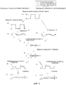
Фиг.1(a), (b) являются блок-схемами для иллюстрации схемы обнаружения изменения емкости настоящего изобретения.1 (a), (b) are block diagrams for illustrating a capacitance change detection circuit of the present invention.
Фиг.2 является принципиальной схемой для иллюстрации схемы обнаружения изменения емкости настоящего изобретения.2 is a circuit diagram for illustrating a capacitance change detection circuit of the present invention.
Фиг.3(a)-(j) являются графиками для иллюстрации действий схемы, показанной на фиг.2.Figure 3 (a) - (j) are graphs for illustrating the actions of the circuit shown in figure 2.
Описание номеров ссылокDescription of reference numbers
1 - схема обнаружения определения изменения емкости,1 is a detection circuit for determining a change in capacitance,
2 - блок ввода,2 - input unit,
3 - средство инверсии фазы,3 - phase inversion means,
41 - средство усиления,41 - means of amplification,
5А, 5В - средства обнаружения,5A, 5B - detection means,
6А, 6В - средства вывода.6A, 6B are output means.
Лучший вариант осуществления изобретенияThe best embodiment of the invention
Схема обнаружения изменения емкости настоящего изобретения описывается с использованием фиг.1(a), (b).The capacitance change detection circuit of the present invention is described using FIGS. 1 (a), (b).
Фиг.1(a), (b) являются блок-схемами для иллюстрации схемы обнаружения изменения емкости настоящего изобретения. Схема 1 обнаружения изменения емкости (в дальнейшем может упоминаться просто как схема 1 обнаружения) согласно настоящему изобретению оснащена набором контактных электродов (в дальнейшем могут упоминаться просто как электроды) А и В. Схема 1 обнаружения также оснащена одним блоком 2 ввода для ввода входного сигнала; одним средством 3 инверсии фазы для инвертирования фазы сигнала (задержки фазы на половину периода); средством 41 усиления для усиления амплитуды введенного сигнала; средством 5А обнаружения для выявления сигнала, показывающего состояние электрода А, из введенного сигнала; средством 5В обнаружения для выявления сигнала, показывающего состояние электрода В, из введенного сигнала; блоками 6А, 6В вывода.1 (a), (b) are block diagrams for illustrating a capacitance change detection circuit of the present invention. The capacitance change detection circuit 1 (hereinafter simply referred to as detection circuit 1) according to the present invention is equipped with a set of contact electrodes (hereinafter simply referred to as electrodes) A and B. The
В схеме 1 обнаружения электроды А и В выполнены, например, на поверхности тактильной панели, и человек может касаться или контактировать с ними. Блок 2 ввода подключен к электроду А и также подключен к электроду В через точку X1 соединения. Одно средство 3 инверсии фазы для инвертирования фазы сигнала подключено только между электродом А и точкой X1 соединения. Также, электрод А подключен к входной стороне средства 41 усиления. Электрод В также подключен к входной стороне средства 41 усиления через точку Х2 соединения между электродом А и средством 41 усиления. Это средство 41 усиления подключено на своей выходной стороне к входным сторонам двух средств 5А и 5В обнаружения через точку Х3 соединения. Кроме того, соответствующие средства 5А, 5В обнаружения подключены на своих выходных сторонах к соответствующим блокам 6А, 6В вывода.In the
Таким образом, схема 1 обнаружения настоящего изобретения имеет очень простую конфигурацию, в которой одно средство усиления и два средства обнаружения предусмотрены для одного набора электродов.Thus, the
Для вышеуказанной схемы 1 обнаружения, как показано на фиг.1(a), при отсутствии контакта или касания от человека, входной сигнал из блока ввода вводится в электрод А через средство 3 инверсии фазы и в электрод В непосредственно, после чего эти введенные сигналы комбинируются в точке Х2 соединения. В этом случае сигнал, подаваемый в электрод А, и сигнал, подаваемый в электрод В, сдвигаются по фазе на половину периода. После комбинирования в точке Х2 соединения амплитуды сигналов нейтрализуются для удержания постоянного напряжения. Даже когда это напряжение подается на средство 41 усиления, усиление результирующего композитного сигнала не осуществляется. Этот сигнал постоянного напряжения ветвится в точке Х3 соединения, и результирующие ответвленные сигналы вводятся в средства 5А и 5В обнаружения. Средство 5А обнаружения уравновешивает сигнал, показывающий состояние электрода В, с фазой, противоположной фазе сигнала, показывающего состояние электрода А, обнаруживает только сигнал, показывающий состояние электрода А, и выводит его в блок 6А вывода (подробности поясняются ниже). Средство 5В обнаружения уравновешивает сигнал, показывающий состояние электрода А, с фазой, противоположной фазе сигнала, показывающего состояние электрода В, обнаруживает только сигнал, показывающий состояние электрода В, из сигнала, выведенного из средства 41 усиления, и выводит его в блок. 6В вывода (подробности поясняются ниже). Соответствующие блоки 6А и 6В вывода определяют то, что контакт не осуществлен.For the
Когда человек контактирует или касается электрода А, как показано на фиг.1(b), достигается состояние, идентичное подключению конденсатора С к электроду А, посредством чего емкости в электродах А и В изменяются. В этом случае входной сигнал из блока 2 ввода вводится в электрод А через средство 3 инверсии фазы и вводится в электрод В непосредственно, после чего эти введенные сигналы комбинируются в точке Х2 соединения. В отличие от вышеописанного случая по фиг.1(a), тем не менее, их амплитуды не уравновешены, так что амплитуда композитного сигнала усиливается посредством средства 41 усиления. Затем, в средстве 5А обнаружения, только сигнал, показывающий состояние электрода А, выявляется из одного усиленного сигнала, выведенного из средства 41 усиления, и выводится в блок 6А вывода (подробности поясняются ниже). В средстве 5В обнаружения только сигнал, показывающий состояние электрода В, выявляется из одного усиленного сигнала и выводится в модуль блок 6В вывода (подробности поясняются ниже).When a person contacts or touches electrode A, as shown in FIG. 1 (b), a state is achieved that is identical to the connection of capacitor C to electrode A, whereby the capacitances in electrodes A and B are changed. In this case, the input signal from the
Таким образом, схема 1 обнаружения настоящего изобретения выполнена таким образом, что сигнал с фазой, противоположной фазе сигнала для электрода В, вводится в электрод А посредством средства 3 инверсии фазы. Вследствие этой конфигурации в средствах 5А, 5В обнаружения, сигналы, показывающие состояния электродов противоположных фаз, подавляются из одного композитного сигнала, и только сигналы, показывающие состояния соответствующих электродов А и В с одной фазой (сигналы, связанные с изменениями емкости), могут извлекаться. Как результат, может быть реализована простая конфигурация, в которой только одно средство усиления предусмотрено для набора электродов.Thus, the
Подробное пояснение для этой схемы 1 обнаружения с использованием фиг.2. Фиг.2 - это принципиальная схема для иллюстрации конкретной конфигурации вышеописанной схемы обнаружения изменения емкости. На фиг.2 идентичным составляющим элементам, показанным на фиг.1(a), 1(b), назначаются ссылки с номером или обозначения, идентичные показанным на фиг.1(a), 1(b).A detailed explanation for this
Фиг.2 показывает три набора электродов, а именно случай, где выбрано 6 электродов, например, когда все соответствующие электроды A-F являются одинаковыми.Figure 2 shows three sets of electrodes, namely the case where 6 electrodes are selected, for example, when all the respective electrodes A-F are the same.
Конфигурация схемы описывается просто в отношении электродов А и В.The configuration of the circuit is described simply with respect to electrodes A and B.
Блок 2 ввода подключен к электроду А и, между электродом А и блоком 2 ввода, одно средство 3 инверсии фазы и резистор R1 подключены в этой последовательности со стороны блока 2 ввода. Средство 3 инверсии фазы выполнено с возможностью инвертировать фазу введенного сигнала и содержит, например, инвертор IN31 на C-MOS. Инвертор IN31 имеет входную сторону, подключенную к блоку 2 ввода, и имеет выходную сторону, подключенную к резистору Ri.The
Блок 2 ввода также подключен к электроду В только через резистор R2 через точку X1 соединения, находящуюся между блоком 2 ввода и средством 3 инверсии фазы. Таким образом, электрод А и электрод В выполнены с возможностью принимать сигналы, имеющие фазы, сдвинутые относительно друг друга на половину периода.The
Кроме того, резистор R11 подключен к электроду А, а резистор R12 подключен к электроду В. Резистор R11 подключен к входной стороне одного средства 41 усиления, а резистор R12 подключен к входной стороне средства 41 усиления через точку Х2 соединения, находящуюся между резистором R11 и входной стороной одного средства 41 усиления. В этой точке Х2 соединения сигнал, показывающий состояние электрода А, и сигнал, показывающий состояние электрода В, комбинируются, и результирующий композитный сигнал вводится в одно средство 41 усиления.In addition, resistor R 11 is connected to electrode A, and resistor R12 is connected to electrode B. Resistor R 11 is connected to the input side of one amplification means 41, and resistor R 12 is connected to the input side of amplification means 41 through a connection point X 2 located between resistor R 11 and the input side of one means 41 gain. At this connection point X 2 , a signal indicating the state of electrode A and a signal showing the state of electrode B are combined, and the resulting composite signal is input into one amplification means 41.
Средство 41 усиления содержит конденсатор С41, инвертор IN41 и резистор R41. Конденсатор С41 подключен к точке Х2 соединения и входной стороне инвертора IN41, и резистор R41 подключен параллельно с инвертором IN41. Инвертор IN41 и резистор R41 составляют схему инвертирующего усиления с отрицательной обратной связью. Вследствие такой конфигурации сигнал, введенный в средство 41 усиления, имеет инвертированную фазу и усиленную амплитуду для вывода.The gain means 41 comprises a capacitor C 41 , an inverter IN 41, and a resistor R 41 . The capacitor C 41 is connected to the connection point X 2 and the input side of the inverter IN 41 , and the resistor R 41 is connected in parallel with the inverter IN 41 . The IN 41 inverter and the R 41 resistor form a negative feedback inverting amplification circuit. Due to this configuration, the signal input to the amplification means 41 has an inverted phase and an amplified amplitude for output.
Выходная сторона средства 41 усиления подключена к двум средствам 5А и 5В обнаружения посредством точки Х3 соединения, находящейся на выходной стороне. Таким образом, сигнал, выведенный из средства 41 усиления, разветвляется снова в точке Х3 соединения, чтобы вводиться в соответствующее средство 5А и 5В обнаружения. Резистор R21 подключен между средством 41 усиления и средством 5А обнаружения, тогда как резистор R22 подключен между средством 41 усиления и средством 5В обнаружения.The output side of the amplification means 41 is connected to the two detection means 5A and 5B via the connection point X 3 located on the output side. Thus, the signal outputted from the amplification means 41 branches out again at the connection point X 3 so as to be input to the corresponding detection means 5A and 5B. A resistor R 21 is connected between the amplification means 41 and the detection means 5A, while a resistor R 22 is connected between the amplification means 41 and the detection means 5B.
В соответствующих средствах 5А и 5В обнаружения, сигналы, показывающие состояния соответствующих электродов А и В, выявляются из одного сигнала, выведенного из средства 41 усиления. С этой целью средства 5А и 5В обнаружения выполнены таким образом, что средство 5А обнаружения должно принимать сигнал для уравновешивания сигнала, показывающего состояние в электроде В, с фазой, противоположной фазе сигнала, подаваемого в электрод А, тогда как средство 5В обнаружения должно принимать сигнал для уравновешивания сигнала, показывающего состояние электрода А, с фазой, противоположной фазе сигнала, подаваемого в электрод В. Таким образом, средство 5А обнаружения выполнено с возможностью обнаруживать только сигнал, показывающий состояние электрода А, тогда как средство 5В обнаружения выполнено с возможностью обнаруживать только сигнал, показывающий состояние электрода В. Как описано выше, средства обнаружения выполнены с возможностью извлекать сигналы в соответствующих электродах. Таким образом, число средств обнаружения соответствует числу электродов.In the respective detection means 5A and 5B, signals showing the states of the respective electrodes A and B are detected from one signal output from the amplification means 41. To this end, the detection means 5A and 5B are configured such that the detection means 5A must receive a signal to balance the signal showing the state of the electrode B with a phase opposite to that of the signal supplied to the electrode A, while the detection means 5B must receive a signal for balancing a signal indicating the state of electrode A with a phase opposite to that of the signal supplied to electrode B. Thus, the detection means 5A is configured to detect only a signal showing the first state of the electrode A, while the detection means 5B is configured to detect only a signal indicating the state of the electrode B. As described above, the detection means are configured to extract signals in the respective electrodes. Thus, the number of detection means corresponds to the number of electrodes.
В частности, средство 5А обнаружения содержит диод D51, резистор R51 и конденсатор С51. Резистор R51 подключен к резистору R21. Диод D51 имеет сторону анода, подключенную к точке X51 соединения, находящейся между резистором R51 и резистором R21, и имеет сторону катода, подключенную к точке Х4 соединения, предусмотренной на выходной стороне средства 3 инверсии фазы. Конденсатор C51 и резистор R51 составляют сглаживающую схему.In particular, the detection means 5A comprises a diode D 51 , a resistor R 51, and a capacitor C 51 . Resistor R 51 is connected to resistor R 21 . The diode D 51 has an anode side connected to the connection point X 51 located between the resistor R 51 and the resistor R 21 , and has a cathode side connected to the connection point X 4 provided on the output side of the phase inversion means 3. Capacitor C 51 and resistor R 51 constitute a smoothing circuit.
В средстве 5А обнаружения сконструированном таким образом сигнал с фазой, идентичной фазе сигнала, подаваемого в электрод А, подается через диод D51. Из этого сигнала только сигнал части низкого напряжения комбинируется в точке X51 соединения с сигналом, выведенным из средства 41 усиления. Этот сигнал части низкого напряжения имеет фазу, противоположную фазе сигнала, показывающего состояние электрода В. Таким образом, из сигнала, выведенного из средства 41 усиления, сигнал, показывающий состояние электрода В, нейтрализуется посредством этого компонента сигнала. Таким образом, этот сигнал части низкого напряжения является сигналом для уравновешивания сигнала, показывающего состояние электрода В. Вследствие этого сигнала только сигнал, показывающий состояние электрода А, может извлекаться в средстве 5А обнаружения. Этот извлеченный сигнал сглаживается посредством резистора R51 и конденсатора C51, и выявляется амплитуда в электроде А.In the
Средство 5В обнаружения, конкретно, содержит диод D52, резистор R52 и конденсатор С52. Резистор R52 подключен к резистору R22. Диод D52 имеет сторону анода, подключенную к точке Х52 соединения, находящейся между резистором R52 и резистором R22, и имеет сторону катода, подключенную к точке Х5 соединения, предусмотренной между блоком 2 ввода и точкой X1 соединения. Конденсатор С52 и резистор R52 составляют сглаживающую схему.The detection means 5B specifically comprises a diode D 52 , a resistor R 52, and a capacitor C 52 . Resistor R 52 is connected to resistor R 22 . The diode D 52 has an anode side connected to the connection point X 52 located between the resistor R 52 and the resistor R 22 , and has a cathode side connected to the connection point X 5 provided between the
В средстве 5В обнаружения, сконструированном таким образом, сигнал с фазой, идентичной фазе сигнала, подаваемого в электрод В, подается через диод D52. Из этого сигнала только сигнал части низкого напряжения комбинируется в точке Х52 соединения с сигналом, выведенным из средства 41 усиления. Сигнал части низкого напряжения сдвинут на половину периода от фазы сигнала, показывающего состояние электрода А. Таким образом, из сигнала, выведенного из средства 41 усиления, сигнал, показывающий состояние электрода А, нейтрализуется посредством сигнала части низкого напряжения. Таким образом, этот сигнал части низкого напряжения является сигналом для уравновешивания сигнала, показывающего состояние электрода А. Вследствие этого сигнала только сигнал, показывающий состояние электрода В, может извлекаться в средстве 5В обнаружения. Этот извлеченный сигнал сглаживается посредством резистора R52 и конденсатора С52, и выявляется амплитуда в электроде В.In the detection means 5B thus constructed, a signal with a phase identical to that of the signal supplied to the electrode B is supplied through the diode D 52 . From this signal, only the signal of the low-voltage part is combined at the connection point X 52 with the signal output from the amplification means 41. The signal of the low voltage part is shifted half the period from the phase of the signal indicating the state of electrode A. Thus, from the signal output from the amplification means 41, the signal showing the state of electrode A is neutralized by the signal of the low voltage part. Thus, this signal of the low voltage portion is a signal for balancing a signal indicating the state of the electrode A. Due to this signal, only a signal indicating the state of the electrode B can be extracted in the detection means 5B. This extracted signal is smoothed out by a resistor R 52 and a capacitor C 52 , and an amplitude is detected in the electrode B.
Выходные стороны средств 5А, 5В обнаружения подключены к блокам 6А, 6В вывода соответственно. Блоки 6А, 6В вывода выполнены с возможностью сравнивания сигналов, выведенных из средств 5А, 5В обнаружения, с опорным сигналом. Когда сигнал, идентичный опорному сигналу, вводится в блоки 6А, 6В вывода, выполняется определение отсутствия контакта. Когда сигналы, отличающиеся от опорного сигнала, вводятся, определяется то, что контакт установлен. Здесь, опорный сигнал является сигналом, идентичным, сигналу, введенному из средства 5А, 5В обнаружения в блоки 6А, 6В вывода, когда контакт с электродами А и В отсутствует.The output sides of the detection means 5A, 5B are connected to
Вышеуказанные пояснения ограничены электродами А и В, но электроды С и D и электроды Е и F также выполнены идентично электродам А и В.The above explanations are limited to electrodes A and B, but electrodes C and D and electrodes E and F are also identical to electrodes A and B.
Электрод С и электрод D, параллельный с электродом С, и будут описаны кратко. Блок 2 ввода подключен к электроду С через средство 3 инверсии фазы, а резистор R3 и блок 2 ввода подключены к электроду D через резистор R4. Электроды С и D подключены к входной стороне одного средства 42 усиления через резисторы R13 и R14 соответственно. Средство 42 усиления содержит конденсатор С42, резистор R42 и инвертор IN42 и имеет конфигурацию, идентичную средству 41 усиления. К выходной стороне средства 42 усиления подключены резистор R23 и входная сторона средства 5С обнаружения, и резистор R24, и входная сторона средства 5D обнаружения также подключены. Выходные стороны средства 5С и 5D обнаружения подключены к блокам 6С и 6D вывода соответственно. Средство 5С обнаружения содержит диод D53, резистор R53 и конденсатор С53 и имеет конфигурацию, идентичную средству 5А обнаружения. Средство 5D обнаружения содержит диод D54, резистор R54 и конденсатор C54 и имеет конфигурацию, идентичную средству 5В обнаружения.The electrode C and the electrode D parallel with the electrode C will be described briefly. The
Электрод Е и электрод F, параллельный с электродом Е, будут описаны кратко. Блок 2 ввода подключен к электроду Е через средство 3 инверсии фазы, а резистор R5 и блок 2 ввода подключены к электроду D через резистор R6. Электроды Е и F подключены к входной стороне одного средства 43 усиления через резисторы R15 и R16 соответственно. Средство 43 усиления содержит конденсатор С43, резистор R43 и инвертор IN43 и имеет конфигурацию, идентичную средству 41 усиления. К выходной стороне средства 43 усиления подключены резистор R25 и входная сторона средства 5Е обнаружения, и также подключены резистор R26 и входная сторона средства 5F обнаружения. Выходные стороны средства 5Е и 5F обнаружения подключены к блокам 6Е и 6F вывода соответственно. Средство 5Е обнаружения содержит диод D55, резистор R55 и конденсатор С55 и имеет конфигурацию, идентичную средству 5А обнаружения. Средство 5F обнаружения содержит диод D56, резистор R56 и конденсатор С56 и имеет конфигурацию, идентичную средству 5В обнаружения.Electrode E and electrode F parallel to electrode E will be described briefly. The
Действия схемы 1 обнаружения изменения емкости, показанной на фиг.2, описываются с использованием фиг.3(a)-3(j), причем описания ограничены электродами А и В. Фиг.3(a)-3(j) являются графиками, показывающими формы волны сигналов в позициях (a)-(j) на фиг.2.The actions of the capacitance
Сперва описываются действия при отсутствии контакта в любом из электродов. Начальные прямоугольные импульсы, введенные из блока 2 ввода, имеют амплитуду с максимальным значением VH и минимальным значением VL (см. фиг.3(a)). Этот входной сигнал разветвляется в точке X1 соединения, после чего один из разветвленных сигналов вводится в инвертор IN31 как средство 3 инверсии фазы и задерживается на половину периода в инверторе IN3i (см. фиг.3(b)). Затем задержанный сигнал подается в электрод А через резистор R1. Таким образом, амплитуда прямоугольных импульсов уменьшается до V2-V1 (см. сигнал, указанный посредством сплошной линии на фиг.3(c)). С другой стороны, входной сигнал, ответвленный в точке X1 соединения, подается в электрод В через резистор R2, так что амплитуда прямоугольных импульсов уменьшается до V1-V3 (см. сигнал, указанный посредством сплошной линии на фиг.3(d)). Здесь, значения резисторов R1 и R2 задаются таким образом, что соответствующие напряжения удовлетворяют соотношениям V1=(VH+VL)/2, V2=3(VH+VL)/4 и V3=(VH+VL)/4, и, предпочтительно, значения резистора R1 и резистора R2 являются одинаковыми.First, actions are described in the absence of contact in any of the electrodes. The initial rectangular pulses introduced from the
Затем сигналы, подаваемые в соответствующие электроды А и В, комбинируются в точке Х2 соединения. Поскольку эти сигналы имеют инвертированные фазы относительно друг друга, результирующий композитный сигнал становится постоянным при напряжении V1 (неизменяющемся постоянном напряжении), как указано сплошной линией на фиг.3(e). Композитный сигнал не имеет амплитуды и, даже когда введен в средство 41 усиления, становится постоянным при напряжении Vi без изменения е* напряжения в позиции (е) (см. фиг.3(f)).Then, the signals supplied to the respective electrodes A and B are combined at the connection point X 2 . Since these signals have inverted phases relative to each other, the resulting composite signal becomes constant at voltage V 1 (constant voltage), as indicated by the solid line in Fig. 3 (e). The composite signal has no amplitude and, even when introduced into the amplification means 41, becomes constant at the voltage Vi without changing the voltage e * at the position (e) (see Fig. 3 (f)).
Затем сигнал вводится в средствах 5А, 5В обнаружения. Действия средства 5А обнаружения описываются далее. В точке Х51 соединения средства 5А обнаружения комбинируются, сигнал, который введен из блока 2 ввода, прошел через инвертор IN31 для инверсии фазы, и затем подан через диод D51, и который состоит только из части напряжения VL, и сигнал, выведенный из средства 41 усиления (см. фиг.3(f)). После комбинирования сигнал, показывающий состояние электрода В, удаляется из сигнала, выведенного из средства 41 усиления, посредством чего только сигнал, показывающий состояние электрода А, извлекается. В позиции (g), получается сигнал с прямоугольной формой импульса, имеющий амплитуду VL-V1, показанный на фиг.3(g) и имеющий период, идентичный периоду сигнала, подаваемого в электрод А.Then, the signal is inputted to the detection means 5A, 5B. The actions of the detection means 5A are described below. At the connection point X 51, the detection means 5A are combined, the signal that is input from the
Когда этот сигнал сглаживается посредством резистора R51 и конденсатора С51, обнаруживается постоянное напряжение, постоянное при напряжении V3 (см. фиг.3(h)). В этом случае только напряжение, идентичное опорному напряжению, вводится в блок 6А вывода. Таким образом, определяется то, что контакт с электродом А отсутствует.When this signal is smoothed out by the resistor R 51 and the capacitor C 51 , a constant voltage is detected, constant at voltage V3 (see FIG. 3 (h)). In this case, only a voltage identical to the reference voltage is inputted to the
В средстве 5В обнаружения, в точке Х52 соединения, комбинируются сигнал, выводимый из средства 41 усиления, и сигнал, который состоит только из части напряжения VL и который подан через диод D52 после ввода входного сигнала (см. фиг.3(b)). В позиции (i), следовательно, получается сигнал с прямоугольной формой импульса, имеющий амплитуду VL-V1, показанный на фиг.3(i).In the detection means 5B, at the connection point X 52 , a signal output from the amplification means 41 and a signal that consists of only part of the voltage V L and which is supplied through the diode D 52 after the input signal is input are combined (see FIG. 3 (b )). At position (i), therefore, a rectangular waveform is obtained having an amplitude V L −V 1 shown in FIG. 3 (i).
Когда этот сигнал сглаживается посредством резистора R52 и конденсатора С52, обнаруживается постоянное напряжение, постоянное при напряжении V3 (см. фиг.3(j)). В этом случае только напряжение, идентичное опорному напряжению, вводится в блок 6В вывода. Таким образом, определяется то, что контакт с электродом В отсутствует.When this signal is smoothed out by means of a resistor R 52 and a capacitor C 52 , a constant voltage is detected, constant at a voltage of V 3 (see FIG. 3 (j)). In this case, only a voltage identical to the reference voltage is input to the
Случай, где человек касается или контактирует с электродом А или В, описывается далее.A case where a person touches or contacts the electrode A or B is described below.
При наличии контакта человека с электродом А или В достигается состояние, идентичное подключению конденсатора С к электроду, как показано на фиг.1(b). В результате, электрический ток протекает в этом конденсаторе С и затем напряжение достигает насыщения. Таким образом, формы волны входных сигналов в электродах А и В становятся сигналами с непрямоугольной формой импульса, как указано посредством пунктирных линий на фиг.3(c) и 3(d).In the presence of human contact with the electrode A or B, a state is achieved that is identical to the connection of the capacitor C to the electrode, as shown in figure 1 (b). As a result, an electric current flows in this capacitor C and then the voltage reaches saturation. Thus, the waveforms of the input signals in the electrodes A and B become signals with a non-rectangular pulse shape, as indicated by the dashed lines in FIGS. 3 (c) and 3 (d).
Когда сигналы форм, указанных посредством пунктирных линий на фиг.3(c) и 3(d), комбинированы в точке Х2 соединения, в качестве центра, формируется сигнал с непрямоугольной формой импульса, имеющий амплитуду со значениями, варьирующимися вверх и вниз от напряжения V1, как указано посредством пунктирных линий на фиг.3(e).When the waveforms indicated by the dashed lines in FIGS. 3 (c) and 3 (d) are combined at the connection point X 2 , as a center, a signal with a non-rectangular waveform having an amplitude with values varying up and down from the voltage is formed V 1 , as indicated by dashed lines in FIG. 3 (e).
Когда результирующий композитный сигнал, указанный посредством пунктирных линий на фиг.3(e), вводится в средство 41 усиления, он имеет инвертированную фазу и усиленную амплитуду, становясь сигналом, имеющим амплитуду VL-VH, с центром в напряжении V1 (см. части с пунктирными линиями на фиг.3(f)). Затем усиленный сигнал разветвляется в точке Х3 соединения и результирующие разветвленные сигналы вводятся в средства 5А и 5В обнаружения через резисторы R21 и R22.When the resulting composite signal indicated by dashed lines in FIG. 3 (e) is input to the amplification means 41, it has an inverted phase and amplified amplitude, becoming a signal having an amplitude V L −V H centered on voltage V 1 (cm parts with dashed lines in Fig. 3 (f)). Then, the amplified signal branches out at the connection point X3 and the resulting branched signals are input to the detection means 5A and 5B through the resistors R 21 and R 22 .
Действия средства 5А обнаружения при наличии контакта с электродом А описываются далее. В точке X51 соединения комбинируются сигнал, который получен из начального входного сигнала, прошел через инвертор IN31 для инверсии фазы, за которым следует прохождение через диод D51, и который состоит только из части напряжения VL, и сигнал, выведенный из средства 41 усиления. Следовательно, сигнал, показывающий состояние электрода В, с фазой, противоположной фазе сигнала в электроде А, уравновешивается посредством сигнала, состоящего только из части напряжения VL. В позиции (g), отображается только сигнал, показывающий состояние электрода А, имеющего большую амплитуду на величину усиленного сигнала, чем тогда, когда контакт отсутствует, как показано посредством пунктирной линии на фиг.3(g).The actions of the detection means 5A in the presence of contact with the electrode A are described below. At connection point X 51, the signal that is obtained from the initial input signal is passed through the inverter IN 31 to phase invert, followed by passing through the diode D 51 , and which consists of only part of the voltage V L , and the signal output from means 41 gain. Therefore, a signal showing the state of the electrode B, with a phase opposite to that of the signal in the electrode A, is balanced by a signal consisting of only part of the voltage V L. At position (g), only a signal is displayed showing the state of electrode A having a larger amplitude by the magnitude of the amplified signal than when there is no contact, as shown by the dashed line in FIG. 3 (g).
Когда этот сигнал сглаживается посредством конденсатора С51, обнаруживается постоянное напряжение (V3+VA), превышающее напряжение V3 на величину усиленного сигнала (см. фиг.3(h)). Как результат, напряжение, превышающее опорное напряжение (V3) на VA, вводится в блок 6А вывода. Таким образом, определяется то, что контакт с электродом А осуществлен.When this signal is smoothed by capacitor C 51 , a constant voltage (V 3 + V A ) is detected that exceeds the voltage V 3 by the magnitude of the amplified signal (see FIG. 3 (h)). As a result, a voltage exceeding the reference voltage (V 3 ) by V A is inputted to the
Действия средства 5В обнаружения при наличии контакта с электродом В описываются далее. В точке Х52 соединения комбинируются сигнал, выводимый из средства 41 усиления, и сигнал, который получен из начального входного сигнала, введенного через диод D51, и который состоит только из части напряжения VL. Сигнал, показывающий состояние электрода А, с фазой, противоположной фазе сигнала, подаваемого в электрод В, из сигнала, выведенного из средства 41 усиления, уравновешивается посредством сигнала, состоящего только из части напряжения VL. В позиции (i) получается сигнал, показывающий состояние электрода В, с формой волны, указанной посредством пунктирной линии на фиг.3(i). Когда эта форма волны сглаживается посредством конденсатора С52, обнаруживается постоянное напряжение (V3+VB), превышающее напряжение V3 на величину усиленного сигнала (см. фиг.3(j)). Следовательно, напряжение, превышающее опорное напряжение (V3) на VB, выводится в блок 6В вывода. Таким образом, определяется то, что контакт с электродом В осуществлен.The actions of the detection means 5B in the presence of contact with the electrode B are described below. At connection point X 52, the signal output from the amplification means 41 is combined with a signal that is obtained from the initial input signal input through the diode D 51 and which consists of only part of the voltage V L. A signal showing the state of the electrode A, with a phase opposite to that of the signal supplied to the electrode B, from the signal output from the amplification means 41 is balanced by a signal consisting of only part of the voltage V L. At position (i), a signal is obtained showing the state of electrode B with the waveform indicated by the dashed line in FIG. 3 (i). When this waveform is smoothed by the capacitor C 52 , a constant voltage (V 3 + V B ) is detected, which exceeds the voltage V 3 by the magnitude of the amplified signal (see FIG. 3 (j)). Therefore, a voltage exceeding the reference voltage (V 3 ) by V B is output to the
Вышеприведенные описания ограничены электродами А и В, но электроды С и D и электроды Е и F также демонстрируют идентичные действия.The above descriptions are limited to electrodes A and B, but electrodes C and D and electrodes E and F also exhibit identical actions.
Для схемы 1 обнаружения, как описано выше, сигналы, которые должны подаваться на два электрода, сдвигаются по фазе относительно друг друга на половину периода посредством средства 3 инверсии фазы и затем комбинируются. При отсутствии контакта амплитуда входных импульсов игнорируется. При наличии контакта амплитуда входных импульсов усиливается посредством одного средства 41 усиления.For the
Средства 5А, 5В обнаружения извлекают только сигналы, показывающие состояния соответствующих электродов. Затем блоки 6А, 6В вывода определяют, обнаружены или нет напряжения выше на усиление входных импульсов, т.е. выше на VA или VB, чем опорное напряжение V3. На основе этого определения, изменения емкости в контактных электродах А и В могут независимо обнаруживаться, и определение может быть выполнено.Detection means 5A, 5B only extract signals indicative of the states of the respective electrodes. Then, the output blocks 6A, 6B determine whether or not the voltage is higher by amplifying the input pulses, i.e. higher by V A or V B than the reference voltage V 3 . Based on this determination, capacitance changes in contact electrodes A and B can be independently detected, and determination can be made.
Следовательно, схема 1 обнаружения настоящего изобретения может обнаруживать наличие или отсутствие контакта с электродом на основе очень простой конфигурации, в которой одно средство усиления и два средства обнаружения предусмотрены для двух электродов.Therefore, the
Для настоящей схемы 1 обнаружения изменения емкости каждое средство не использует сам транзистор, а состоит из только одного диода, инвертора, резистора, конденсатора.For the
Для настоящей схемы 1 обнаружения изменения емкости, кроме того, может быть логически определено то, присутствует контакт или нет, в зависимости от того, какой из двух уровней напряжения выводится в блоках 6А-6F вывода, а именно, напряжение, идентичное опорному напряжению, или более высокое напряжение, чем опорное напряжение, как в цифровой схеме. Таким образом, настоящая схема 1 обнаружения изменения емкости имеет преимущество в том, что сбои практически не возникают.For the current capacitance
Для вышеуказанной схемы 1 обнаружения предпочтительно, чтобы значения резисторов R1-R6 были одинаковыми. Также предпочтительно, чтобы значения R11-R16 были одинаковыми, и значения R21-R26 тоже были одинаковыми. Также предпочтительно, чтобы значения R1-R6 и R11-R16 также были одинаковыми.For the
На фиг.2, электроды А и В, электроды С и D и электроды Е и F разделены на пары и подключены к каждому средству 41 усиления. Тем не менее, комбинация электродов может быть любой комбинацией, которая дает возможность подачи сигналов различных фаз в электроды.In FIG. 2, electrodes A and B, electrodes C and D, and electrodes E and F are paired and connected to each amplification means 41. However, the combination of electrodes can be any combination that allows signals of various phases to be supplied to the electrodes.
Кроме того, если требуется такая операция, как осуществление одновременного контакта с двумя или более контактными электродами, например, если требуется такая операция для одновременного включения электродов А и В как переключателей, электроды А и С и электроды В и D могут быть выполнены с возможностью становиться набором контактных электродов, соответственно. Таким образом, конфигурируется так, что сигнал из блока 2 ввода разветвляется в точке X1 соединения и вводится в электроды С и D, а сигнал, имеющий фазу, инвертированную посредством средства 3 инверсии фазы, вводится в электроды А и В. Затем конфигурируется так, что сигнал, показывающий состояние электрода А, и сигнал, показывающего состояние электрода С, вводятся в средство 41 усиления, и сигнал, показывающий состояние электрода В, и сигнал, показывающий состояние электрода D, вводятся в средство 42 усиления.In addition, if an operation such as simultaneous contact with two or more contact electrodes is required, for example, if such an operation is required to simultaneously turn on the electrodes A and B as switches, the electrodes A and C and the electrodes B and D can be made to become a set of contact electrodes, respectively. Thus, it is configured so that the signal from the
Посредством такого конфигурирования схемы обнаружения одновременный контакт может быть обнаружен. В этом случае может быть получен идентичный эффект, даже если компоновка электродов А и В изменяется. Таким образом, если контактные электроды А, С, В и D размещаются в этой последовательности на фиг.2, может быть получен эффект, идентичный упомянутому выше. Если одновременный контакт с электродами А и В возникает в случае, где не требуется такая операция, как выполнение одновременного контакта с двумя или более контактными электродами, то в точке Х2 соединения комбинация сигналов, показывающих состояния соответствующих электродов, приводит к постоянному напряжению. Этот результат идентичен результату, возникающему при отсутствии контакта с электродами А и В. В этом случае, следовательно, результирующие данные могут быть обнаружены, например, как ошибка ввода, при условии, что контакт отсутствует.By such configuration of the detection circuit, simultaneous contact can be detected. In this case, an identical effect can be obtained even if the arrangement of the electrodes A and B changes. Thus, if the contact electrodes A, C, B, and D are arranged in this sequence in FIG. 2, an effect identical to that mentioned above can be obtained. If simultaneous contact with electrodes A and B occurs in the case where an operation such as simultaneous contact with two or more contact electrodes is not required, then at point X 2 the combination of signals showing the state of the respective electrodes leads to a constant voltage. This result is identical to the result that occurs when there is no contact with electrodes A and B. In this case, therefore, the resulting data can be detected, for example, as an input error, provided that there is no contact.
Если вышеописанная настоящая схема обнаружения 1 используется в качестве тактильной панели, например тактильной панели как переключателя для аудиосистемы в автомобиле, электроды предусмотрены только на поверхности секции панели тактильной панели так, чтобы человек мог касаться или контактировать с ними, и блоки вывода подключены к блоку управления аудио. Настоящая схема 1 обнаружения проста в настройке и упрощает интеграцию, даже если число электродов увеличивается. Таким образом, настоящая схема 1 обнаружения является подходящей для конструирования схем со многими входами, таких как переключатель для аудиосистемы. Соответствующие электроды могут быть предусмотрены, например, в позиции, допускающей косвенный контакт, к примеру на тыловой поверхности секции панели или внутри тактильной панели, без расположения на поверхности секции панели.If the above-described
В вышеописанном варианте осуществления контакты в контактных электродах были обнаружены в соответствующем средстве обнаружения. Тем не менее, схема 1 обнаружения может быть настроена, например, таким образом, чтобы разность напряжений между блоками 6А и 6В вывода обнаруживалась, и на основе этой разности напряжений может быть определено то, присутствуют или нет контакты в контактных электродах А, В.In the above embodiment, the contacts in the contact electrodes were detected in an appropriate detection means. However, the
Промышленная применимостьIndustrial applicability
Настоящая схема может использоваться как тактильный датчик в органических EL-пластинах, тактильных панелях (например, в дисплейных панелях оборудования и переключателях для аудиосистем, установленных на автомобилях) и т.д. Таким образом, настоящая схема может быть использована в области техники промышленного оборудования.This circuit can be used as a tactile sensor in organic EL plates, tactile panels (for example, in equipment display panels and switches for car audio systems), etc. Thus, the present scheme can be used in the field of industrial equipment technology.
Claims (10)
по меньшей мере, один набор контактных электродов, включающий в себя набор из первого контактного электрода, на который подается импульсный сигнал из блока ввода для импульсного сигнала через средство инверсии фазы, и второго контактного электрода, на который подается импульсный сигнал из блока ввода;
одно средство усиления, подключенное к одному набору контактных электродов;
первое средство обнаружения для обнаружения сигнала, показывающего состояние первого контактного электрода;
второе средство обнаружения для обнаружения сигнала, показывающего состояние второго контактного электрода; и
блоки вывода, подключенные к первому средству обнаружения и второму средству обнаружения, соответственно.1. A circuit for detecting a change in capacitance comprising:
at least one set of contact electrodes, including a set of a first contact electrode, to which a pulse signal is supplied from an input unit for a pulse signal through phase inversion means, and a second contact electrode, to which a pulse signal is supplied from an input unit;
one gain means connected to one set of contact electrodes;
first detection means for detecting a signal indicating a state of the first contact electrode;
second detection means for detecting a signal indicating a state of the second contact electrode; and
output units connected to the first detection means and the second detection means, respectively.
средство усиления содержит инвертор, конденсатор, предусмотренный на входной стороне инвертора, и резистор, параллельный с инвертором, выходная сторона инвертора подключена к входным сторонам средства обнаружения, и
инвертор и резистор составляют схему инвертирующего усиления с отрицательной обратной связью.2. The detection circuit of the change in capacity according to claim 1, in which:
the amplification means comprises an inverter, a capacitor provided on the input side of the inverter, and a resistor parallel to the inverter, the output side of the inverter is connected to the input sides of the detection means, and
the inverter and resistor form a negative feedback inverting amplification circuit.
средство инверсии фазы содержит инвертор.3. The detection circuit of the change in capacity according to claim 1, in which:
the phase inversion means comprises an inverter.
каждое из первого и второго средства обнаружения содержит диод, резистор и конденсатор,
диод первого средства обнаружения имеет сторону катода, подключенную к первой точке соединения, на которую подается импульсный сигнал из средства инверсии фазы, и имеет сторону анода, подключенную ко второй точке соединения, предусмотренной между выходной стороной средства усиления и резистором первого средства обнаружения,
диод второго средства обнаружения имеет сторону катода, подключенную к третьей точке соединения, на которую подается импульсный сигнал из блока ввода, и имеет сторону анода, подключенную к четвертой точке соединения, предусмотренной между выходной стороной средства усиления и резистором второго средства обнаружения, и
резистор и конденсатор каждого средства обнаружения составляют сглаживающую схему.4. The detection circuit of the change in capacity according to claim 1, in which:
each of the first and second detection means comprises a diode, a resistor and a capacitor,
the diode of the first detection means has a cathode side connected to a first connection point to which a pulse signal from the phase inversion means is supplied, and has an anode side connected to a second connection point provided between an output side of the amplification means and a resistor of the first detection means,
the diode of the second detection means has a cathode side connected to a third connection point to which a pulse signal is supplied from the input unit, and has an anode side connected to a fourth connection point provided between the output side of the amplification means and the resistor of the second detection means, and
the resistor and capacitor of each detection means constitute a smoothing circuit.
первый резистор предусмотрен между средством инверсии фазы и первым контактным электродом,
второй резистор предусмотрен между блоком ввода и вторым контактным электродом, и
первый резистор и второй резистор имеют одинаковое значение сопротивления.5. The detection circuit of the change in capacity according to claim 1, in which:
a first resistor is provided between the phase inversion means and the first contact electrode,
a second resistor is provided between the input unit and the second contact electrode, and
the first resistor and the second resistor have the same resistance value.
третий резистор предусмотрен между первым контактным электродом и средством усиления,
четвертый резистор предусмотрен между вторым контактным электродом и средством усиления, и
третий резистор и четвертый резистор имеют одинаковое значение сопротивления.6. The detection circuit of the change in capacity according to claim 1, in which:
a third resistor is provided between the first contact electrode and the amplification means,
a fourth resistor is provided between the second contact electrode and the amplification means, and
the third resistor and the fourth resistor have the same resistance value.
в которой:
первый резистор, второй резистор, третий резистор и четвертый резистор имеют одинаковое значение сопротивления.7. The detection circuit changes capacitance according to claim 6,
wherein:
the first resistor, the second resistor, the third resistor and the fourth resistor have the same resistance value.
пятый резистор предусмотрен между средством усиления и первым средством обнаружения,
шестой резистор предусмотрен между средством усиления и вторым средством обнаружения, и
пятый резистор и шестой резистор имеют одинаковое значение сопротивления.8. The detection circuit of the change in capacity according to claim 1, in which:
a fifth resistor is provided between the amplification means and the first detection means,
a sixth resistor is provided between the amplification means and the second detection means, and
the fifth resistor and the sixth resistor have the same resistance value.
схему обнаружения изменения емкости по п.1;
секцию панели; и
блок управления, и
в котором контактные электроды схемы обнаружения изменения емкости предусмотрены в секции панели, и
блоки вывода схемы обнаружения изменения емкости подключены к блоку управления.9. A tactile panel comprising:
a capacitance change detection circuit according to claim 1;
panel section; and
control unit, and
in which the contact electrodes of the capacitance change detection circuit are provided in the panel section, and
the output blocks of the capacitance change detection circuit are connected to the control unit.
обнаружение сигнала, показывающего разность между сигналом, показывающим состояние первого контактного электрода, и сигналом, показывающим состояние второго контактного электрода; и
определение, на основе сигнала, показывающего разность, того, имеется или нет контакт с каким-либо из контактных электродов. 10. A determination method for determining whether or not there is contact with a contact electrode by using a capacitance change detection circuit according to claim 1, comprising
detecting a signal showing a difference between a signal showing a state of the first contact electrode and a signal showing a state of the second contact electrode; and
determining, based on the signal showing the difference, whether or not there is contact with any of the contact electrodes.
Applications Claiming Priority (2)
| Application Number | Priority Date | Filing Date | Title |
|---|---|---|---|
| JP2007264112A JP4941938B2 (en) | 2007-10-10 | 2007-10-10 | Capacitance change detection circuit, touch panel, and determination method |
| JP2007-264112 | 2007-10-10 |
Publications (1)
| Publication Number | Publication Date |
|---|---|
| RU2433526C1 true RU2433526C1 (en) | 2011-11-10 |
Family
ID=40549221
Family Applications (1)
| Application Number | Title | Priority Date | Filing Date |
|---|---|---|---|
| RU2010118585/08A RU2433526C1 (en) | 2007-10-10 | 2008-10-08 | Capacitance variation detection circuit, tactile panel and method of detection |
Country Status (7)
| Country | Link |
|---|---|
| US (1) | US8587553B2 (en) |
| JP (1) | JP4941938B2 (en) |
| KR (1) | KR101126508B1 (en) |
| CN (1) | CN101821947B (en) |
| DE (1) | DE112008002731B4 (en) |
| RU (1) | RU2433526C1 (en) |
| WO (1) | WO2009048077A1 (en) |
Families Citing this family (6)
| Publication number | Priority date | Publication date | Assignee | Title |
|---|---|---|---|---|
| KR101499024B1 (en) * | 2012-11-28 | 2015-03-06 | 에이디반도체(주) | Electrostatic Capacitance Sensor |
| JP6115888B2 (en) * | 2013-03-29 | 2017-04-19 | Toto株式会社 | Capacitive touch sensor |
| JP6168470B2 (en) * | 2013-03-29 | 2017-07-26 | Toto株式会社 | Capacitive touch sensor |
| DE102017105957B3 (en) | 2017-03-20 | 2018-09-13 | Hochschule Osnabrück | Operating element for switching an electronic device |
| WO2019092953A1 (en) * | 2017-11-10 | 2019-05-16 | アルプスアルパイン株式会社 | Input device |
| CN110612508B (en) * | 2018-02-05 | 2023-06-23 | 深圳市汇顶科技股份有限公司 | Touch controller, demodulation method and touch system |
Family Cites Families (17)
| Publication number | Priority date | Publication date | Assignee | Title |
|---|---|---|---|---|
| US3761736A (en) * | 1971-05-12 | 1973-09-25 | Godwin Warren Engin Ltd | Proximity switches |
| US3781736A (en) * | 1972-10-26 | 1973-12-25 | Gen Electric | Shield for permanent magnet structure |
| JPS629423A (en) * | 1985-07-05 | 1987-01-17 | Seiko Epson Corp | Input and display device |
| JP2733300B2 (en) * | 1989-04-28 | 1998-03-30 | 松下電器産業株式会社 | Key input device |
| GB9209364D0 (en) | 1992-04-30 | 1992-06-17 | Varitronix Ltd | A touch sensitive device |
| US5963277A (en) * | 1996-08-24 | 1999-10-05 | Lg Electronics Inc. | Position sensible liquid crystal display device |
| JP2000295183A (en) * | 1999-03-29 | 2000-10-20 | Gsl Research Technology Ltd | Touch link |
| JP4830228B2 (en) * | 2001-07-30 | 2011-12-07 | オムロン株式会社 | Touch sensor |
| JP2004028719A (en) | 2002-06-25 | 2004-01-29 | Tdk Corp | Electrostatic capacity sensor |
| CN1287522C (en) * | 2002-12-20 | 2006-11-29 | 阿尔卑斯电气株式会社 | Inputting device with electrostatic sensor |
| JP2004206288A (en) * | 2002-12-24 | 2004-07-22 | Alps Electric Co Ltd | Electronic equipment with input device |
| JP4009953B2 (en) | 2003-05-14 | 2007-11-21 | オムロン株式会社 | Object detection sensor |
| DE102005063023A1 (en) * | 2005-12-14 | 2007-06-21 | Gerd Reime | Arrangement for monitoring an object |
| CN100370402C (en) * | 2005-08-05 | 2008-02-20 | 鸿富锦精密工业(深圳)有限公司 | Touch type inductor |
| US8279180B2 (en) * | 2006-05-02 | 2012-10-02 | Apple Inc. | Multipoint touch surface controller |
| US7812827B2 (en) * | 2007-01-03 | 2010-10-12 | Apple Inc. | Simultaneous sensing arrangement |
| DE102007048402A1 (en) * | 2007-10-09 | 2009-04-16 | Gerd Reime | Control unit and method for triggering a function |
-
2007
- 2007-10-10 JP JP2007264112A patent/JP4941938B2/en not_active Expired - Fee Related
-
2008
- 2008-10-08 RU RU2010118585/08A patent/RU2433526C1/en not_active IP Right Cessation
- 2008-10-08 KR KR1020107010056A patent/KR101126508B1/en active IP Right Grant
- 2008-10-08 DE DE112008002731.5T patent/DE112008002731B4/en not_active Expired - Fee Related
- 2008-10-08 WO PCT/JP2008/068300 patent/WO2009048077A1/en active Application Filing
- 2008-10-08 US US12/680,390 patent/US8587553B2/en not_active Expired - Fee Related
- 2008-10-08 CN CN2008801111875A patent/CN101821947B/en not_active Expired - Fee Related
Also Published As
| Publication number | Publication date |
|---|---|
| JP4941938B2 (en) | 2012-05-30 |
| CN101821947B (en) | 2012-09-05 |
| DE112008002731B4 (en) | 2014-07-10 |
| CN101821947A (en) | 2010-09-01 |
| US20100230180A1 (en) | 2010-09-16 |
| KR20100080554A (en) | 2010-07-08 |
| JP2009094849A (en) | 2009-04-30 |
| DE112008002731T5 (en) | 2010-08-26 |
| KR101126508B1 (en) | 2012-03-29 |
| WO2009048077A1 (en) | 2009-04-16 |
| US8587553B2 (en) | 2013-11-19 |
Similar Documents
| Publication | Publication Date | Title |
|---|---|---|
| RU2433526C1 (en) | Capacitance variation detection circuit, tactile panel and method of detection | |
| US10003334B2 (en) | Capacitative sensor system | |
| KR101749540B1 (en) | Capacitive key touch sensing using analog inputs and digital outputs | |
| US9354758B2 (en) | Mutual capacitive touch panel | |
| US10073574B2 (en) | Methods and apparatus for a capacitive sensor | |
| US9551738B2 (en) | Robust capacitive measurement system | |
| CN110286787B (en) | Control chip for touch panel and operation method thereof | |
| TW201243686A (en) | Touch sensing circuit | |
| ES2729379T3 (en) | Minimum impedance variation detection device | |
| TW201635124A (en) | Capacitive touch device with high sensitivity and operating method thereof | |
| JP2011007753A5 (en) | ||
| KR100992278B1 (en) | ?? emitting type touch switch | |
| US20120062500A1 (en) | Adaptive high dynamic range surface capacitive touchscreen controller | |
| US11592936B2 (en) | Capacitive touch device with high sensitivity and low power consumption | |
| EP2687961B1 (en) | Input device | |
| US9886143B2 (en) | Multi-function sensing apparatus | |
| TW201619791A (en) | Test apparatus for touch panel and test method thereof | |
| JP2009094849A5 (en) | ||
| US9035894B2 (en) | Touch sensing and feedback apparatuses and methods | |
| US20100013355A1 (en) | "push button switch" | |
| US20120139867A1 (en) | Capacitive touch apparatus | |
| JP5033489B2 (en) | Capacitance change detection circuit | |
| JP2008198063A (en) | Coordinate position detector | |
| US8711123B2 (en) | Multi-touch recognition resistive touch screen for recognizing multi-touch coordinates through capacitor charging time | |
| JP4811987B2 (en) | CV conversion circuit |
Legal Events
| Date | Code | Title | Description |
|---|---|---|---|
| MM4A | The patent is invalid due to non-payment of fees |
Effective date: 20201009 |