RU2127946C1 - Transceiver switching circuit and its functioning process - Google Patents
Transceiver switching circuit and its functioning process Download PDFInfo
- Publication number
- RU2127946C1 RU2127946C1 RU94046113A RU94046113A RU2127946C1 RU 2127946 C1 RU2127946 C1 RU 2127946C1 RU 94046113 A RU94046113 A RU 94046113A RU 94046113 A RU94046113 A RU 94046113A RU 2127946 C1 RU2127946 C1 RU 2127946C1
- Authority
- RU
- Russia
- Prior art keywords
- circuit
- transceiver
- transmitter
- control signal
- receiver
- Prior art date
Links
Images
Classifications
-
- H—ELECTRICITY
- H04—ELECTRIC COMMUNICATION TECHNIQUE
- H04B—TRANSMISSION
- H04B1/00—Details of transmission systems, not covered by a single one of groups H04B3/00 - H04B13/00; Details of transmission systems not characterised by the medium used for transmission
- H04B1/38—Transceivers, i.e. devices in which transmitter and receiver form a structural unit and in which at least one part is used for functions of transmitting and receiving
- H04B1/40—Circuits
- H04B1/44—Transmit/receive switching
- H04B1/48—Transmit/receive switching in circuits for connecting transmitter and receiver to a common transmission path, e.g. by energy of transmitter
Abstract
Description
Настоящее изобретение относится, главным образом, к схемам коммутации и, более конкретно, к коммутационной цепи приемопередатчика, например приемопередатчика, выполненного с возможностью передавать и принимать коммуникационные сигналы в течение чередующихся периодов времени. The present invention relates mainly to switching circuits and, more specifically, to a switching circuit of a transceiver, for example a transceiver, configured to transmit and receive communication signals for alternating periods of time.
Система связи состоит, как минимум, из передатчика и приемника, соединенных между собой каналом связи. Коммуникационный сигнал передается передатчиком по каналу связи для приема приемником. Система радиосвязи является системой связи, в которой канал связи содержит радиочастотный канал, определяемый границами частот электромагнитного частотного спектра. Радиопередатчик, работающий в системе радиосвязи, должен преобразовать коммуникационный сигнал в форму, приемлемую для передачи по радиочастотному каналу. A communication system consists, at a minimum, of a transmitter and a receiver, interconnected by a communication channel. The communication signal is transmitted by the transmitter over the communication channel for reception by the receiver. A radio communication system is a communication system in which a communication channel comprises a radio frequency channel defined by frequency boundaries of the electromagnetic frequency spectrum. A radio transmitter operating in a radio communication system must convert the communication signal into a form suitable for transmission over the radio frequency channel.
Преобразование коммуникационного сигнала в форму, пригодную для передачи по радиочастотному каналу, осуществляется с помощью модуляции. При модуляции передаваемый сигнал накладывается на электромагнитное колебание, электромагнитное колебание называется "несущим сигналом". Результирующим сигнал, промодулированный коммуникационным сигналом, обычно называется модулированным несущим сигналом. Передатчик содержит схемы, позволяющие осуществить модуляцию. The conversion of the communication signal into a form suitable for transmission over the radio frequency channel is carried out using modulation. When modulated, the transmitted signal is superimposed on the electromagnetic wave, the electromagnetic wave is called the "carrier signal". The resulting signal modulated by the communication signal is usually called a modulated carrier signal. The transmitter contains circuits that allow modulation.
Так как модулированный несущий сигнал может передаваться в пространстве на большие расстояния, системы радиосвязи широко используются для осуществления связи между передатчиком и удаленным приемником. Since the modulated carrier signal can be transmitted in space over long distances, radio communication systems are widely used to communicate between a transmitter and a remote receiver.
Приемник системы радиосвязи, которым принимает модулированный несущий сигнал, содержит схемы, аналогичные схемам передатчика, но действующие инверсно по сравнению с ними и реализующие процесс демодуляции. The receiver of the radio communication system, which receives the modulated carrier signal, contains circuits similar to those of the transmitter, but acting inversely compared to them and implementing the demodulation process.
Многочисленные модулированные несущие сигналы могут одновременно передаваться по различным радиочастотным каналам электромагнитного частотного спектра. Специальные регуляторы делят части электромагнитного частотного спектра на полосы частот и регулируют передачу модулированных несущих сигналов по различным частотным полосам. (Частотные полосы далее делятся на каналы, и такие каналы формируют радиочастотные каналы системы радиосвязи. Такие каналы иногда будут называться ниже термином "стандартно определенные частотные каналы".)
Система двухсторонней радиосвязи является системой связи, подобной вышеописанной системе радиосвязи, но обеспечивает как передачу и прием модулированного несущего сигнала в некоторой точке, так и прием модулированного несущего сигнала в указанной точке. Каждый пункт такой двухсторонней системы радиосвязи содержит и передатчик, и приемник. Передатчик и приемник, размещаемые в одной точке, обычно содержат блок, называемый радиоприемопередатчиком, или, проще говоря, приемопередатчиком.Numerous modulated carrier signals can be transmitted simultaneously on various radio frequency channels of the electromagnetic frequency spectrum. Special regulators divide parts of the electromagnetic frequency spectrum into frequency bands and regulate the transmission of modulated carrier signals over different frequency bands. (Frequency bands are further divided into channels, and such channels form the radio frequency channels of a radio communication system. Such channels will sometimes be referred to below as the term "standardly defined frequency channels".)
A two-way radio communication system is a communication system similar to the above-described radio communication system, but provides both transmission and reception of a modulated carrier signal at some point, and reception of a modulated carrier signal at a specified point. Each point of such a two-way radio communication system contains both a transmitter and a receiver. A transmitter and a receiver located at one point typically contain a unit called a radio transceiver, or, more simply, a transceiver.
Сотовая система связи является одним из типов систем двухсторонней радиосвязи, в котором разрешена связь с приемопередатчиком, размещенным в любой точке географической зоны, охваченной сотовой системой связи. A cellular communication system is one type of two-way radio communication system in which communication with a transceiver located anywhere in the geographical area covered by a cellular communication system is allowed.
Сотовая система связи создается размещением множества зафиксированных на одном месте радиоприемопередатчиков, называемых базовыми станциями или базовыми позициями на разнесенных в пространстве пунктах по географической зоне. Базовые станции соединены с обычной проводной телефонной сетью. Все, что связано с каждой базовой станцией множества базовых станций, является частью географической зоны, охваченном сотовой системой связи. Такие части называются ячейками. Каждая из множества ячеек определяется одной из базовых станции множества базовых станций, а все множество ячеек определяет площадь покрытия сотовой системы связи. A cellular communication system is created by placing a plurality of radio transmitters fixed in one place, called base stations or base positions at spatially separated points in a geographical area. Base stations are connected to a regular wired telephone network. Everything associated with each base station of a plurality of base stations is part of a geographical area covered by a cellular communication system. Such parts are called cells. Each of the plurality of cells is determined by one of the base stations of the plurality of base stations, and the entire plurality of cells determines the coverage area of the cellular communication system.
Радиоприемопередатчик, называемый в сотовой системе связи сотовым радиотелефоном, или, проще, сотовым телефоном, размещенным в любой точке в пределах площади покрытия сотовой системы связи, способен связываться с пользователем обычной проводной телефонной сети при помощи базовой станции. Модулированные несущие сигналы, вырабатываемые радиотелефоном, передаются базовой станции, а модулированные несущие сигналы, вырабатываемые базовой станцией, передаются радиотелефону. Тем самым, обеспечивается двухсторонняя связь между ними. (Сигнал, принятый базовой станцией, затем передается в требуемую точку расположения обычной проводной сети при помощи методов обычной телефонии. Сигналы, вырабатываемые в точке расположения проводной сети, передаются на базовую станцию с использованием методов телефонии, после чего передаются базовой станцией на радиотелефон). A radio transceiver, called a cellular radiotelephone in a cellular communication system, or, more simply, a cellular telephone located anywhere within the coverage area of a cellular communication system, is capable of communicating with a user of a conventional wired telephone network using a base station. Modulated carrier signals generated by the radiotelephone are transmitted to the base station, and modulated carrier signals produced by the base station are transmitted to the radiotelephone. Thus, a two-way communication between them is provided. (The signal received by the base station is then transmitted to the desired location of the conventional wired network using conventional telephony methods. The signals generated at the location of the wired network are transmitted to the base station using telephony methods, and then transmitted by the base station to the radiotelephone).
Возросшее использование сотовых систем связи в некоторых случаях привело к полному использованию каждого доступного канала передачи частотной полосы, предназначенной для сотовой радиотелефонной связи. В результате, предлагались различные идеи более эффективного использования частотной полосы, предназначенной для радиотелефонной связи. При помощи более эффективного использования частотной, полосы, отведенной для радиотелефонной связи, может быть увеличена пропускная способность существующих сотовых систем связи. The increased use of cellular communication systems in some cases has led to the full use of each available transmission channel of the frequency band intended for cellular radiotelephone communication. As a result, various ideas were proposed for more efficient use of the frequency band for radiotelephone communications. By making better use of the frequency band allocated for radiotelephone communications, the throughput of existing cellular communication systems can be increased.
Пропускная способность сотовой системы связи может быть увеличена путем минимизации спектра модуляции модулированного сигнала, передаваемого передатчиком, с целью осуществления одновременной передачи большего числа модулированных сигналов. Кроме того, путем минимизации количества времени, необходимого для передачи модулированного сигнала, может последовательно передаваться большее количество модулированных сигналов. The throughput of a cellular communication system can be increased by minimizing the modulation spectrum of the modulated signal transmitted by the transmitter in order to simultaneously transmit more modulated signals. In addition, by minimizing the amount of time required to transmit the modulated signal, more modulated signals can be transmitted sequentially.
Посредством преобразования коммуникационного сигнала в дискретную форму до его передачи результирующий модулированный сигнал обычно получается более узкого спектра, чем соответствующий модулированный сигнал, содержащий коммуникационный сигнал, не преобразованный в дискретную форму. К тому же, когда коммуникационный сигнал преобразуется в дискретную форму до модуляции, результирующий модулированный сигнал может передаваться короткими пачками импульсов и по одному стандартно определенному частотному каналу может последовательно передаваться более одного модулированного сигнала. (Так как по одному стандартно определенному частотному каналу может передаваться более одного модулированного сигнала, термин "частотный канал" иногда относится к части стандартно определенного частотного канала, в которой отдельный передатчик передает модулированный сигнал отдельному приемнику. Следовательно, в коммуникационной схеме, в которой модулированные сигналы передаются в дискретных пачках импульсов, на одном стандартно определенном частотном канале могут быть определены два или более частотных каналов.)
Так как один частотный канал используется для передачи двух или более отдельных сигналов в течение непересекающихся периодов времени, способ передачи сигнала определяется как способ разделения во времени. Система связи, использующая такой способ разделения во времени передачи сигналов, содержат систему связи множественного многостанционного доступа с разделением времени или, проще, систему связи МДРВ.By converting a communication signal into a discrete form prior to transmission, the resulting modulated signal usually produces a narrower spectrum than the corresponding modulated signal containing a communication signal that is not converted to a discrete form. In addition, when a communication signal is converted to a discrete form before modulation, the resulting modulated signal can be transmitted in short bursts of pulses and more than one modulated signal can be transmitted sequentially through one standardly defined frequency channel. (Since more than one modulated signal can be transmitted over one standardly defined frequency channel, the term “frequency channel” sometimes refers to the part of a standardly defined frequency channel in which a single transmitter transmits a modulated signal to an individual receiver. Therefore, in a communication circuit in which modulated signals transmitted in discrete bursts of pulses, two or more frequency channels can be defined on one standardly defined frequency channel.)
Since a single frequency channel is used to transmit two or more separate signals over non-overlapping time periods, a signal transmission method is defined as a time division method. A communication system using such a time division method of transmitting signals comprises a multi-station access communication system with time division or, more simply, an MDRV communication system.
Система связи МДРВ содержит передатчик, способный передавать сигналы приемнику в перемежающихся пачках в течение дискретных периодов времени. Такой сигнал, передаваемый отдельному приемнику, действующему в системе связи МДРВ, будет называться далее сигналом МДРВ. The communication system MDRV contains a transmitter capable of transmitting signals to the receiver in intermittent packets for discrete periods of time. Such a signal transmitted to an individual receiver operating in an MDRV communication system will hereinafter be referred to as an MDRV signal.
Система связи МДРВ имеет преимущества при использовании в качестве сотовой системы связи, так как в течение периода времени, когда базовая станция не передает сигнал МДРВ отдельному радиотелефону, могут передаваться другие сигналы МДРВ. В частности, радиотелефон, которому базовая станция передает сигнал МДРВ, может, в свою очередь, передавать сигнал МДРВ базовой станции, тем самым обеспечивая двухстороннюю связь между базовой станцией и радиотелефоном по одному стандартно определенному частотному каналу, поскольку сигналы, посылаемые базовой станцией радиотелефону и радиотелефоном базовой станции, могут быть разделены во времени так, чтобы появляться в чередующиеся периоды времени. The TDMA communication system has advantages when used as a cellular communication system, because during the time period when the base station does not transmit the TDMA signal to a separate radiotelephone, other TDMA signals can be transmitted. In particular, the radiotelephone to which the base station transmits the TDMA signal can, in turn, transmit the TDMA signal to the base station, thereby providing two-way communication between the base station and the radiotelephone via one standard frequency channel, since the signals sent by the base station to the radiotelephone and radiotelephone base stations can be divided in time so as to appear in alternating periods of time.
Так как схемы передатчика и приемника, действующего в подобной системе связи МДВР, должны работать только в прерывистом режиме, некоторые части схемы радиотелефонов, действующих в обычных сотовых системах связи, не требуются. К примеру, фильтры дуплексера, установленные для соединения между собой передатчика и приемника обычного сотового радиотелефона с радиотелефонной антенной, не требуются в системах связи МДРВ, так как передающая и приемная части схемы такого радиотелефона не должны работать одновременно. Since the transmitter and receiver circuits operating in such a TDMA communication system should only operate in intermittent mode, some parts of the radiotelephone circuit operating in conventional cellular communication systems are not required. For example, duplexer filters installed to connect a transmitter and a receiver of a conventional cellular radiotelephone to a radiotelephone antenna are not required in MDRV communication systems, since the transmitting and receiving parts of the circuit of such a radiotelephone should not work simultaneously.
Вместо этого может использоваться коммутационная цепь для соединения приемной части схемы с радиотелефонной антенной или передающей части схемы с радиотелефонной антенной. Instead, a switching circuit may be used to connect the receiving portion of the circuit to a radiotelephone antenna or the transmitting portion of the circuit to a radiotelephone antenna.
Стандартные коммутационные схемы, используемые для поочередного соединения приемной или передающей частей схемы с радиотелефонной антенной, состоят из дискретных компонентов или дискретных компонентов вместе со стандартными линиями передачи. В целом, такие коммутационные цепи действуют для поочередного электрического соединения либо приемной, либо передающей частей схемы радиотелефона с радиотелефонной антенной при электрическом изолировании другой части схемы радиотелефона от радиотелефонной антенны. The standard switching circuits used to alternately connect the receiving or transmitting parts of the circuit with a radiotelephone antenna consist of discrete components or discrete components together with standard transmission lines. In general, such switching circuits act to alternately electrically connect either the receiving or transmitting parts of the radiotelephone circuit with the radiotelephone antenna while electrically isolating the other part of the radiotelephone circuit from the radiotelephone antenna.
Однако любая из таких конструкций коммутационных цепей содержит схемные элементы с низкими относительными добротностями (значениями добротности Q) и, следовательно, проявляет значительные вносимые потери. Следовательно, из-за того, что такие цепи часто представлены идеализированными элементами, паразитные эффекты, возникающие из-за наличия паразитных емкостей и индуктивностей, делают такие коммутационные цепи изначально неэффективными. Для преодоления подобной неэффективности традиционных коммутационных цепей усилительные части передающей части радиотелефона должны усиливать сигналы, подлежащие передаче при больших уровнях усиления. Такие большие уровни усиления, однако, дают увеличение потребления энергии радиотелефоном. However, any of these designs of switching circuits contains circuit elements with low relative Q factors (Q values Q) and, therefore, exhibits significant insertion loss. Therefore, due to the fact that such circuits are often represented by idealized elements, parasitic effects arising from the presence of parasitic capacitances and inductances make such switching circuits initially ineffective. To overcome this inefficiency of traditional switching circuits, the amplifying parts of the transmitting part of the radiotelephone must amplify the signals to be transmitted at high amplification levels. Such large gain levels, however, give an increase in energy consumption by the radiotelephone.
Коммутационная цепь с меньшей величиной вносимых потерь обеспечила бы потребление меньших количеств энергии в процессе работы радиотелефона. A switching circuit with a lower insertion loss would allow less energy to be consumed during the operation of the radiotelephone.
Поэтому, необходима коммутационная цепь с меньшей величиной вносимых потерь, чем у стандартных коммутационных цепей. Therefore, you need a switching circuit with a lower insertion loss than standard switching circuits.
Соответственно, в настоящем изобретении раскрыта коммутационная цепь и соответствующий способ, обеспечивающие минимальные вносимые потери. Accordingly, in the present invention, a switching circuit and a corresponding method are disclosed that provide minimal insertion loss.
В настоящем изобретении дополнительно раскрыта коммутационная цепь для приемопередатчика, поочередно соединяющего схемы приемника или передатчика в приемопередатчике с антенной приемопередатчика. The present invention further discloses a switching circuit for a transceiver that alternately connects a receiver or transmitter circuit in a transceiver to a transceiver antenna.
В настоящем изобретении дополнительно приведен радиотелефон с коммутационной цепью для поочередного соединения частей приемника или передатчика схемы радиотелефона с антенной радиотелефона. The present invention further provides a switched telephone radiotelephone for alternately connecting parts of a receiver or transmitter of a radiotelephone circuit to an antenna of a radiotelephone.
Другие преимущества и характеристики заявленного изобретения приведены в описании предпочтительных вариантов выполнения. Other advantages and characteristics of the claimed invention are given in the description of preferred embodiments.
В соответствии с настоящим изобретением описываются коммутационная цепь и соответствующий способ для приемопередатчика со схемами приемника и передатчика. Коммутационная цепь способна переключаться в зависимости от уровня приложенного к ней управляющего сигнала. Коммутационная цепь поочередно соединяет схему передатчика с антенной приемопередатчика или схему приемника с антенной приемопередатчика. Первый участок (элемент) цепи соединяет между собой схему передатчика и первую часть антенны приемопередатчика, причем первый элемент цепи имеет электрические характеристики, зависящие от уровней управляющего сигнала. Второй участок цепи соединяет между собой схему приемника и первую часть антенны приемопередатчика, причем, в зависимости от уровней управляющего сигнала, второй участок цепи содержит как свою часть шунтирующую цепочку. Передающая линия управляющего сигнала расположена по крайней мере на одной керамической подложке, соединенной с первым участком цепи, для приложения по этой линии управляющего сигнала к первому участку цепи. Первый участок цепи формирует замыкание для электрического соединения схемы передатчика и антенны приемопередатчика, а также шунтирование для формирования части второго участка цепи, чтобы тем самым электрически отключить схему приемника от антенны приемопередатчика только на то время, когда управляющий сигнал превышает первый уровень сигнала. В противном случае, первый участок цепи формирует размыкание для электрического отключения схемы передатчика и антенны приемопередатчика, а также для отключения шунта от второго участка цепи, чтобы, тем самым, электрически соединить схему приемника и антенну приемопередатчика. In accordance with the present invention, a switching circuit and a corresponding method for a transceiver with receiver and transmitter circuits are described. The switching circuit is capable of switching depending on the level of the control signal applied to it. A switching circuit alternately connects the transmitter circuit to the transceiver antenna or the receiver circuit to the transceiver antenna. The first section (element) of the circuit interconnects the transmitter circuit and the first part of the transceiver antenna, and the first circuit element has electrical characteristics that depend on the levels of the control signal. The second section of the circuit connects the receiver circuit and the first part of the antenna of the transceiver, and, depending on the levels of the control signal, the second section of the circuit contains as part of a shunt chain. The transmission line of the control signal is located on at least one ceramic substrate connected to the first section of the circuit, for application along this line of the control signal to the first section of the circuit. The first section of the circuit forms a short circuit for the electrical connection of the transmitter circuit and the transceiver antenna, as well as shunting to form part of the second section of the circuit, thereby electrically disconnecting the receiver circuit from the transceiver antenna only for a time when the control signal exceeds the first signal level. Otherwise, the first section of the circuit forms an opening to electrically disconnect the transmitter circuit and the transceiver antenna, as well as to disconnect the shunt from the second circuit section, thereby electrically connecting the receiver circuit and the transceiver antenna.
Настоящее изобретение в дальнейшем поясняется описанием предпочтительных вариантов выполнения изобретения со ссылками на сопровождающие чертежи, на которых:
Фиг.1 изображает электрическую принципиальную схему коммутационной цепи, состоящей из дискретных компонентов, образующей эквивалентную схему, соответствующую электрической принципиальной схеме коммутационной цепи согласно предпочтительному варианту выполнения настоящего изобретения.The present invention is further illustrated by the description of preferred embodiments of the invention with reference to the accompanying drawings, in which:
Figure 1 depicts an electrical circuit diagram of a switching circuit consisting of discrete components forming an equivalent circuit corresponding to an electrical circuit diagram of a switching circuit according to a preferred embodiment of the present invention.
Фиг.2 - электрическую принципиальную схему коммутационной цепи, подобную цепи по фиг. 1, но в которой часть коммутационной цепи содержит передающую линию. FIG. 2 is an electrical circuit diagram of a switching circuit similar to that of FIG. 1, but in which a part of the switching circuit comprises a transmission line.
Фиг. 3 - электрическую принципиальную схему коммутационной цепи согласно предпочтительному варианту выполнения настоящего изобретения. FIG. 3 is an electrical circuit diagram of a switching circuit according to a preferred embodiment of the present invention.
Фиг.4 - схематический вид множества размещенных друг за другом элементов керамической платы, которые вместе образуют коммутационную цепь согласно предпочтительному варианту выполнения изобретения. Figure 4 is a schematic view of a plurality of ceramic board elements arranged one after another, which together form a switching circuit according to a preferred embodiment of the invention.
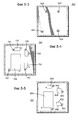
Фиг. 5-1 - вид сверху первого элемента керамической платы из множества элементов керамической платы коммутационной цепи, показанной на фиг.4, с частью размещенной на нем коммутационной цепи по фиг.3. FIG. 5-1 is a plan view of a first element of a ceramic board from a plurality of elements of a ceramic board of the switching circuit shown in FIG. 4, with a portion of the switching circuit of FIG. 3 placed thereon.
Фиг.5-2 - вид сверху, подобный приведенному на фиг.5-1, но второго элемента керамической платы из множества элементов керамической платы коммутационной цепи, показанной на фиг.4, с частью размещенной на нем коммутационной цепи по фиг.3. Fig. 5-2 is a top view similar to that shown in Fig. 5-1, but the second element of the ceramic board of the plurality of ceramic circuit board elements shown in Fig. 4, with a part of the switching circuit located on it in Fig. 3.
Фиг.5-3 - вид сверху, подобный приведенному на фиг.5-1 и 5-2, но третьего элемента керамической платы коммутационной цепи, показанной на фиг.4, с частью размещенной на нем коммутационной цепи. Fig.5-3 is a top view similar to that shown in Fig.5-1 and 5-2, but the third element of the ceramic circuit board circuit shown in Fig.4, with part of the circuit located on it.
Фиг. 5-4 - вид сверху, подобный приведенному на фиг.5-1 - 5-3, но четвертого элемента керамической платы из множества элементов керамической платы коммутационной цепи по фиг.3 и 4. FIG. 5-4 is a plan view similar to that shown in FIGS. 5-1 to 5-3, but of the fourth element of the ceramic board from the plurality of elements of the ceramic circuit board of FIG. 3 and 4.
Фиг. 5-5 - вид сверху, подобный приведенному на фиг.5-1 - 5-4, но пятого элемента керамической платы из множества элементов керамической платы коммутационной цепи по фиг.3 и 4. FIG. 5-5 is a plan view similar to that shown in FIGS. 5-1 to 5-4, but of the fifth element of the ceramic board from the plurality of elements of the ceramic circuit board of the switching circuit of FIGS. 3 and 4.
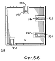
Фиг.5-6 - вид сверху, подобный приведенному на фиг.5-1 - 5-5, но шестого элемента керамической платы из множества элементов керамической платы коммутационной цепи по фиг.3 и 4. Fig.5-6 is a top view similar to that shown in Fig.5-1 to 5-5, but the sixth element of the ceramic board of the many elements of the ceramic circuit board of the switching circuit of Fig.3 and 4.
На фиг.1 изображена электрическая принципиальная схема, в которую входит радиоприемопередатчик, обозначенный позицией 100. Радиоприемопередатчик 100 может, к примеру, содержать радиотелефон, работающий в сотовой системе связи. Figure 1 shows an electrical circuit diagram, which includes a radio transceiver, indicated by the position 100. The radio transceiver 100 may, for example, contain a radiotelephone operating in a cellular communication system.
Радиоприемопередатчик 100 содержит коммутационную цепь 106, состоящую из элементов, содержащихся внутри пунктирного блока, обозначенного позицией 106, для поочередного соединения схемы 112 передатчика с антенной 118 приемопередатчика. В зависимости от установки коммутационной цепи 106 радиоприемопередатчик 100 работает либо на передачу сигнала, вырабатываемого схемой 112 передатчика, через антенну 118 приемопередатчика, либо на подачу сигнала, переданного на антенну 118 приемопередатчика (извне), на схему 124 приемника. Поскольку приемопередатчик поочередно передает и принимает сигналы, приемопередатчик 100 использует схему связи МДРВ. The radio transceiver 100 comprises a switching circuit 106 consisting of elements contained within a dotted block, indicated by 106, for alternately connecting the transmitter circuit 112 to the transceiver antenna 118. Depending on the installation of the switching circuit 106, the radio transceiver 100 operates either to transmit a signal generated by the transmitter circuit 112 through the transceiver antenna 118, or to provide a signal transmitted to the transceiver antenna 118 (from the outside) to the receiver circuit 124. Since the transceiver alternately transmits and receives signals, the transceiver 100 uses a TDMA communication scheme.
Элементы, составляющие коммутационную цепь 106, показаны в виде дискретных элементов. Последовательно соединенные конденсатор 130 и диод 136 образуют вместе первый участок цепи, представленный блоком 142 в пунктирной рамке, который соединяет между собой схему 112 передатчика и антенну 118 приемопередатчика. Конденсатор 130 имеет такую емкость, чтобы получался блокирующий конденсатор постоянного тока, который формирует разомкнутую цепь для сигналов постоянного тока, но который шунтирует высокочастотные сигналы. Анодный вывод диода 136 соединен с конденсатором 130, а катодный вывод диода 136 - с антенной 118 приемопередатчика с помощью конденсатора 146. Конденсатор 146 имеет емкость, позволяющую осуществлять замыкание для высоких частот и размыкание на уровнях постоянного тока. Диод 136 образует замкнутую цепь, только если на диод подают положительное смещение. В остальных случаях диод 136 образует разомкнутую цепь. The elements making up the switching circuit 106 are shown as discrete elements. The series-connected capacitor 130 and diode 136 together form a first section of the circuit, represented by a dotted frame in block 142, which connects the transmitter circuit 112 and the transceiver antenna 118 to each other. The capacitor 130 has such a capacity that a blocking DC capacitor is obtained, which forms an open circuit for DC signals, but which shunts high-frequency signals. The anode terminal of the diode 136 is connected to the capacitor 130, and the cathode terminal of the diode 136 is connected to the transceiver antenna 118 using the capacitor 146. The capacitor 146 has a capacitance that allows short circuiting at high frequencies and opening at DC levels. Diode 136 forms a closed circuit only if a positive bias is applied to the diode. In other cases, the diode 136 forms an open circuit.
Коммутационная цепь 106, кроме того, содержит последовательно соединенные индуктивность 148 и конденсатор 152, а также шунтирующие конденсаторы 158 и 164 и диод 170. Конденсатор 152, сходный с конденсатором 130, имеет такую емкость, чтобы образовать блокирующий постоянный ток конденсатор. Конденсатор 152 образует разомкнутую цепь для сигналов постоянного тока, формируя в то же время замкнутую цепь для высокочастотных сигналов. Диод 170 формирует замкнутую цепь, если к его анодному выводу приложено положительное напряжение, тем самым диод 170 формирует шунтирующую цепь для заземления в случае приложения положительного напряжения; в остальных случаях диод 170 формирует разомкнутую цепь. The switching circuit 106 further comprises a series-connected inductance 148 and a capacitor 152, as well as shunt capacitors 158 and 164 and a diode 170. The capacitor 152, similar to the capacitor 130, has such a capacitance to form a DC blocking capacitor. The capacitor 152 forms an open circuit for DC signals, while at the same time forming a closed circuit for high-frequency signals. The diode 170 forms a closed circuit if a positive voltage is applied to its anode terminal, thereby the diode 170 forms a shunt circuit for grounding if a positive voltage is applied; in other cases, the diode 170 forms an open circuit.
Индуктивность 148, конденсаторы 152, 158 и 164 и диод 170 вместе образуют второй участок 176 цепи, соединяющий между собой схему 124 приемника и антенну 118 приемопередатчика. Inductance 148, capacitors 152, 158, and 164 and diode 170 together form a second circuit portion 176 connecting the receiver circuit 124 and the transceiver antenna 118.
Коммутационная цепь 106 дополнительно содержит индуктивность 182, образующую высокочастотный дроссель. Первый вывод индуктивности 182 соединен с узлом между конденсатором 130 и диодом 136 первого плеча 142 цепи. Второй вывод индуктивности 182 соединен с источником напряжения, показанным блоком 188, идентифицируемым как управляющее напряжение. Величина управляющего напряжения от источника питания определяет, подключена ли к антенне 118 приемопередатчика схема 112 передатчика или схема 124 приемника. Величина управляющего напряжения определяется, к примеру, процессором (не показан на чертеже) приемопередатчика 100. Если определено, что приемопередатчик 100 должен передавать сигнал, такой процессор вырабатывает сигнал, чтобы сделать управляющее напряжение напряжением высокого уровня, а если определено, что приемопередатчик 100 должен принимать переданный ему сигнал, процессор вырабатывает сигнал, чтобы сделать управляющее напряжение низким. (Т.е. высокий уровень напряжения является уровнем, достаточным для прямого смещения диодов 136 и 170.)
В процессе работы, когда приемопередатчик 100 должен передавать сигнал, управляющее напряжение, подаваемое на индуктивность 182, имеет большую положительную величину. Указанное напряжение заставляет диоды 136 и 170 иметь очень низкий импеданс (полное внутреннее сопротивление), а следовательно, эффективно формировать замкнутые цепи. (Для простоты диоды далее будут обозначаться либо как замкнутые, либо как разомкнутые цепи, хотя такие элементы и имеют очень низкие или очень высокие текущие значения импедансов). Тем самым, первое плечо 142 цепи электрически соединяет схему 112 передатчика с антенной 118 приемопередатчика, а шунтовая цепь, сформированная диодом 170, заземляет схему 124 приемника. Узел, сформированный соединением индуктивности 148 и конденсатора 158, также имеет высокий импеданс, тогда как узел, сформированный соединением индуктивности 148, конденсаторов 152 и 164 и диода 170, имеет низкий импеданс. Сигналы, вырабатываемые схемой 112 передатчика (модулированные на высоких частотах), тем самым, подаются на антенну 118 приемопередатчика для передачи с нее.The switching circuit 106 further comprises an inductance 182 forming a high-frequency inductor. The first inductance 182 is connected to a node between the capacitor 130 and the diode 136 of the first arm 142 of the circuit. The second inductance terminal 182 is connected to a voltage source shown by block 188, identified as a control voltage. The magnitude of the control voltage from the power source determines whether the transmitter circuit 112 or the receiver circuit 124 is connected to the transceiver antenna 118. The magnitude of the control voltage is determined, for example, by the processor (not shown in the drawing) of the transceiver 100. If it is determined that the transceiver 100 should transmit a signal, such a processor generates a signal to make the control voltage a high level voltage, and if it is determined that the transceiver 100 should receive the signal transmitted to him, the processor generates a signal to make the control voltage low. (That is, a high voltage level is a level sufficient to direct bias the diodes 136 and 170.)
In operation, when the transceiver 100 is to transmit a signal, the control voltage supplied to the inductance 182 has a large positive value. The specified voltage makes the diodes 136 and 170 have a very low impedance (total internal resistance), and therefore, effectively form closed circuits. (For simplicity, diodes will hereinafter be referred to as either closed or open circuits, although such elements have very low or very high current impedance values). Thus, the first arm 142 of the circuit electrically connects the transmitter circuit 112 to the transceiver antenna 118, and the shunt circuit formed by the diode 170 ground the receiver circuit 124. The assembly formed by connecting the inductance 148 and the capacitor 158 also has a high impedance, while the assembly formed by connecting the inductance 148, the capacitors 152 and 164 and the diode 170 has a low impedance. The signals generated by the transmitter circuit 112 (modulated at high frequencies) are thereby supplied to the transceiver antenna 118 for transmission from it.
Наоборот, если управляющее напряжение имеет низкую величину (к примеру, ноль вольт или близко к нулю), диоды 136 и 170 являются разомкнутыми цепями. Тем самым, схема 112 передатчика электрически изолирована от антенны 118 приемопередатчика. Поскольку диод 170 не образует шунтовой цепи, схема 124 приемника электрически соединяется при помощи второго плеча 176 цепи с антенной 118. Conversely, if the control voltage is low (for example, zero volts or close to zero), the diodes 136 and 170 are open circuits. Thus, the transmitter circuit 112 is electrically isolated from the transceiver antenna 118. Since the diode 170 does not form a shunt circuit, the receiver circuit 124 is electrically connected via the second circuit arm 176 to the antenna 118.
Как отмечено ранее, вследствие того, что цепи состоят из дискретных элементов с низкими значениями Q (т.е. относительными добротностями, кратко отмеченными выше), такие цепи вносят потери на высоких частотах, радиоприемопередатчик типа приемопередатчика 100, имеющий коммутационную цепь типа коммутационной цепи 106, состоящей только из дискретных компонентов, неэффективен из-за больших вносимых потерь на высоких частотах. As noted earlier, due to the fact that the circuits are composed of discrete elements with low Q values (i.e., relative Q factors briefly noted above), such circuits introduce high-frequency losses, a radio transceiver such as transceiver 100, having a switching circuit such as a switching circuit 106 , consisting only of discrete components, is inefficient due to the large insertion loss at high frequencies.
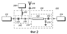
На фиг.2 показан радиоприемопередатчик, обозначенный позицией 200. Радиоприемопередатчик 200 действует подобно радиоприемопередатчику 100 на фиг.1 и содержит коммутационную цепь, в данном случае, коммутационную цепь 206 (состоящую из элементов, показанных в блоке), схему 212 передатчика, антенну 218 приемопередатчика и схему 224 приемника. Figure 2 shows a radio transceiver, indicated by 200.
Коммутационная цепь 206 поочередно соединяет схему 212 передатчика или схему 224 приемника с антенной 218 приемопередатчика. Коммутационная цепь 206 содержит последовательно соединенные конденсатор 230 и диод 236, вместе образующие первый участок 242 цепи, представленный в виде блоков в пунктирной рамке. Первый участок 242 цепи и формирующие его элементы цепи аналогичны первому участку 142 цепи радиоприемопередатчика 100 по фиг.1. Конденсатор 246, аналогичный конденсатору 146 приемопередатчика 100 по фиг.1, также образует часть приемопередатчика 200. The
Коммутационная цепь 206 дополнительно содержит последовательно соединенные передающую линию 250 и конденсатор 252, а также диод 270, размещенный в шунтовой конфигурации. Передающая линия 250, конденсатор 252 и диод 270 вместе образуют второй участок цепи, представленный блоком 276 в пунктирной рамке. Второй участок 276 цепи и составляющие его элементы аналогичны второму участку 176 цепи приемопередатчика 100 по фиг.1. Участки 276 и 176 отличаются лишь тем, что передающая линия 250 заменяет дискретные элементы 148, 158 и 164 второго участка 176 цепи. The
Коммутационная цепь 206 дополнительно содержит индуктивность 282, образующую высокочастотный дроссель. Первый вывод индуктивности 282 соединен с первым участком 242 цепи в узле, образованном между конденсатором 230 и диодом 236. Второй вывод индуктивности 282 соединен с источником напряжения, в данном случае управляющего напряжения, представленным блоком 280. Источник напряжения, представленный блоком 288 управляющего напряжения, и индуктивность 282 аналогичны блоку 188 управляющего напряжения и индуктивности 182 радиоприемопередатчика 100 по фиг.1. The
Работа коммутационной цепи 206 радиоприемопередатчика 200 аналогична работе коммутационной цепи 106 радиоприемопередатчика 100 по фиг.1, поэтому подробности работы цепи 206 детально не описываются. The operation of the
Следует отметить, что передающая линия 250 функционально эквивалентна комбинации конденсаторов 158 и 164 и индуктивности 148 второго участка 176 цепи и может быть альтернативно представлена этими дискретными компонентами. Передающую линию 250 предпочтительно использовать вместо дискретных компонентов ввиду того, что передающая линия дает меньшие вносимые потери, чем соответствующие дискретные компоненты, а вследствие меньшего количества вносимых потерь у линии 250 достигается более эффективное действие коммутационной цепи. Обычно передающая линия 250 состоит из обычной полосковой линии либо из микрополосковой линии. Передающая линия 250 имеет длину, по существу, соответствующую четверти длины волны сигналов, подлежащих передаче антенной 218 приемопередатчика. (Следует отметить, что передающая линия 250 образует открытую цепь на высоких частотах в местоположении четвертьволновой длины высокой частоты, на которой схемой 212 передатчика генерируется передаваемый сигнал, от местоположения короткого замыкания на землю, которое имеет место, когда диод 270 образует короткозамкнутую цепь). Когда диод 270 образует короткозамкнутую цепь, а передающая линия 250 образует разомкнутую цепь на расстоянии четверти длины волны от диода 270, т.е. на выводе передающей линии 250, удаленном от диода 270, антенна 218 приемопередатчика становится изолированной от схемы 224 приемника. It should be noted that the
Однако, хотя передающая линия 250 имеет более высокую величину Q, чем соответствующие дискретные компоненты ключа 106 на фиг.1, и потому вносит меньше потерь, чем соответствующие дискретные компоненты ключа 106 на фиг.1, обычная передающая линия также вносит значительные потери, соответственно, радиоприемопередатчик, подобный радиоприемопередатчику 200, с коммутационной цепью, подобной коммутационной цепи 206, часть которой образована передающей линией, также изначально неэффективен (хотя и в меньшей степени, нежели коммутационная цепь, состоящая только из дискретных компонентов) вследствие большой величины вносимых потерь, связанных с элементами коммутационной цепи. However, although the
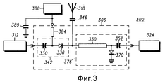
Фиг. 3, представляющая предпочтительный вариант выполнения, иллюстрирует электрическую принципиальную схему радиоприемопередатчика 300, который содержит коммутационную цепь 306, состоящую из элементов, показанных внутри пунктирного блока, схему 312 передатчика и схему 324 приемника. Ключ 306 поочередно подключает схему 312 передатчика к антенне 318 приемопередатчика или схему 324 приемника к антенне 318 приемопередатчика. Коммутационная цепь 306, аналогичная вышеописанным коммутационным цепям, содержит последовательно соединенные конденсатор 330 и диод 336. Конденсатор 330 и диод 336 составляют вместе первый участок 342 цепи, аналогичный первым участкам 242 и 142 из фиг.1, 2. Конденсатор 346, блокирующий постоянный ток, дополнительно показан на чертеже и аналогичен конденсаторам 246 и 146 предыдущих чертежей. FIG. 3, representing a preferred embodiment, illustrates an electrical circuit diagram of a
Коммутационная цепь 306 содержит далее последовательно соединенные передающую линию 350 и конденсатор 352. Конденсатор 352 имеет такую величину емкости, чтобы образовать блокировочный конденсатор, а передающая линия 350 имеет длину, по существу, соответствующую четверти длины волны сигналов, подлежащих передаче антенной 318 приемопередатчика и приему схемой 324 приемника. Кроме того, диод 370 включен в шунтовую конфигурацию таким же образом, как и установка диодов 270 и 170 на предыдущих чертежах. Передающая линия 350, конденсатор 352 и диод 370 образуют вместе второй участок 376 цепи, представленный обведенным пунктиром блоком и функционирующий аналогично вторым участкам 276 и 176 на предыдущих чертежах. The
Коммутационная цепь 306 дополнительно содержит передающую линию 384 с первым выводом, подключенным к узлу, образованному соединением между конденсатором 330 и диодом 336. Второй вывод передающей линии 384 соединен с источником напряжения, которым вновь является управляющее напряжение, представленное блоком 388. Управляющее напряжение также изолировано от земли при помощи конденсатора 389. Подача управляющего напряжения на передающую линию 350 осуществляется тем же образом, что и подача управляющего сигнала на индуктивности 282 и 182 предыдущих чертежей. Передающая линия 384 имеет длину, по существу, соответствующую четверти длины волны сигналов, вырабатываемых схемой 312 передатчика. Конденсатор 389 имеет такую величину, чтобы образовать цепь короткого замыкания на землю на высоких частотах. Передающая линия 384 образует разомкнутую цепь на высоких частотах в положении, расположенном на расстоянии в четверть длины волны высокой частоты переданного сигнала, выработанного схемой 312 передатчика, от положения короткого замыкания на землю. Передающая линия 384 не образует разомкнутой цепи для постоянного тока при управляющем напряжении, выработанном блоком 388 управляющего напряжения. The
Радиоприемопередатчик 300 отличается от радиоприемопередатчика 200 по фиг. 2 не только вследствие замены передающей линией 384 индуктивности 284, но также потому, что передающие линии 350 и 384 сформированы на подложках керамикоподобного материала, а не состоят из обычных полосковых линий или микрополосковых передающих линий. Передающие линии, размещенные на керамикоподобных материалах, вносят существенно меньшие потери, чем соответствующие передающие линии обычной конструкции. Поэтому, радиоприемопередатчик 300 изначально более эффективен, чем радиоприемопередатчики 200 и 100 по предыдущим фигурам. The
Тогда как в предпочтительном варианте выполнения по фиг.3 передающие линии 350 и 384 размещены на керамикоподобных материалах, элементы, составляющие первый и второй участки 342 и 376 цепи, могут быть размещены на одной или более керамических подложках. While in the preferred embodiment of FIG. 3, the
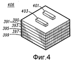
На фиг.4 схематически показана обозначенная позицией 406 коммутационная цепь по предпочтительному варианту выполнения настоящего изобретения. Коммутационная цепь 406 эквивалентна коммутационной цепи 306 по фиг.3, в которой многие элементы, составляющие первый и второй участки 342 и 376 цепи, также (в дополнение к передающим линиям 350 и 384) размещены на керамикоподобных подложках. В варианте выполнения по фиг.4 ключ 406 состоит из шести расположенных друг за другом керамических подложек. Передающие линии 350 и 384 и компоненты первого и второго участков 342 и 376 цепи размещены на различных подложках. 4 schematically shows the switching circuit indicated at 406 according to a preferred embodiment of the present invention. The
Верхняя керамическая подложка 390 расположена над второй керамической подложкой 391, которая в свою очередь расположена над третьей керамической подложкой 393. В свою очередь третья керамическая подложка 393 расположена над четвертой керамической подложкой 395, которая в свою очередь расположена над пятой керамической подложкой 397. Пятая керамическая подложка 397 в свою очередь расположена над донной керамической подложкой 399. The upper
Различные части различных компонентов, соответствующих первому и второму участкам 342 и 376, а также передающая линия 384 коммутационной цели 306 радиоприемопередатчика 300 размещены на различных керамических подложках 390 - 399. Перемычки, образованные дорожками проводящего материала, проходящими через части различных керамических подложек 390 - 399, обеспечивают соединения между компонентами, размещенными на различных подложках 390 - 399. Дискретные диоды (предпочтительно, PIN-диоды) 401 и 403 установлены на верхней поверхности первой керамической подложки 390. Диоды 401 и 403 соответствуют диодам 336 и 370 по фиг.3. После установки керамических подложек 390 - 399 друг за другом в требуемом порядке, показанном на фиг.3 (диоды 401 и 403 установлены на подложке 390), несколько расположенных друг за другом подложек спекаются (т. е. , керамические подложки спекаются в печи) в течение времени, необходимом для получения жесткой конструкции нескольких керамических подложек 390 - 399. The various parts of the various components corresponding to the first and
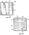
На виде сверху фиг.5-1 показана верхняя поверхность керамической подложки 390. Расположенные на верхней поверхности керамической подложки 390 покрытия из электропроводных материалов отмечены штриховкой частей лицевой поверхности. Как показано, на верхней лицевой поверхности керамической подложки 390 размещены три площадки 412, 414 и 418. Верхние концы перемычек 420, 422 и 426 расположены внутри соответствующей одной из площадок 412 - 418. Площадки 412 и 414 образуют места установки, позволяющие установить на них диод 401 (показанный на фиг.4), а площадка 418 образует место установки, позволяющее установить на нем диод 403 (также показанный на фиг.4). Второй вывод диода 403 установлен на лицевой поверхности подложки 390, которая покрыта электропроводным материалом и задает плоскость заземления. Верхние концы перемычек 420 и 422 обеспечивают подключение диода 401, после его установки в положение на площадках 412 и 414, к остальной схеме, размещенной на других керамических подложках 391 - 399. А перемычка 426 обеспечивает подключение диода 403 после его позиционирования к схеме, размещенной на других керамических пластинах 391 - 399. In the top view of FIGS. 5-1, the upper surface of the
Фиг. 5-2 является видом сверху верхней поверхности второй керамической подложки 391. Подобно предыдущему чертежу, покрытия электропроводного материала на верхней поверхности керамической подложки 391 помечены штриховкой. На лицевой поверхности второй подложки 391 сформированы змеевидные дорожки 550 и 584. Такие дорожки образуют передающие линии, аналогичные передающим линиям 350 и 384 коммутационной цепи 306 по фиг.3. Длины каждой из дорожек соответствуют четверти длины волны сигналов, передаваемых приемопередатчиком, включающим в себя коммутационную цепь 406, частями которой являются дорожки 550 и 584. (В процессе экспериментирования установлено слабое влияние изменений в протяженности змеевидной формы передающих линий на изменения их характеристик; такое изменение может незначительно изменять рабочие данные сформированной таким образом цепи). FIG. 5-2 is a top view of the upper surface of the second
Верхние концы перемычек 586, 588, 590 и 592, которые проходят через подложку 391, также показаны на чертеже. Перемычка 586 размещена с возможностью обеспечить связь с перемычкой 422, перемычка 588 установлена с возможностью обеспечения связи с перемычкой 420. Когда керамические подложки 390 и 391 соединяются друг с другом и устанавливаются вслед друг другу, конец дорожки 584 становится электрически подключенным к диоду 401, установленному на площадку 412 подложки 390, вывод дорожки 550 подобным же образом соединен с диодом 401, установленным на площадке 414, а второй вывод дорожки 550 соединен с диодом 403, установленным на площадке 418. Как отмечено ранее, выполнение передающих линий, образованных дорожками 550 и 584 на керамической подложке, является выгодным, т.к. вносимые потери таким образом выполненной передающей линии значительно ниже, чем вносимые потери обычных передающих линий, образованных полосковыми линиями или микрополосками. The upper ends of the
Фиг. 5-3 является видом сверху верхней лицевой поверхности керамической подложки 393 коммутационной цепи 406 по фиг.4. На верхней лицевой поверхности керамической подложки 393 размещены только верхние концы перемычек 650, 652, 654 и 656. А значительная часть остающейся лицевой поверхности покрыта электропроводным материалом за исключением небольшой изолированной области вокруг верхних концов перемычек 650-656. Из-за размещенного на подложке 393 покрытия электропроводного материала подложка 393 образует изолированную плоскость для изоляции дорожек 550 и 584, которые образуют передающие линии. Перемычки 650-656 служат единственно для соединения соответствующих перемычек 424, 586, 588 и 590 (и соответствующих элементов, подключенных к таким перемычкам) к схемным элементам, размещенным на других подложках 395-399. FIG. 5-3 is a top view of the upper face surface of the
На фиг. 5-4 изображен вид сверху на верхнюю лицевую поверхность керамической подложки 395. Часть верхней лицевой поверхности подложки 395, покрытая покрытием из электропроводного материала, также обозначена на чертеже штриховкой. Как показано, на лицевой поверхности подложки 395 образованы четыре площадки 730, 752, 758 и 789. Каждая из площадок 730-789 образует обкладки конденсаторов 330, 352, 358 и 389 коммутационной цепи 306 по фиг.3. Верхние концы перемычек 791, 793, 795 и 797 также показаны на чертеже. Перемычка 791 установлена для обеспечения соединения с перемычкой 650, перемычка 793 установлена для обеспечения соединения с перемычкой 656, перемычка 795 установлена для обеспечения соединения с перемычкой 652, а перемычка 797 установлена для обеспечения соединения с перемычкой 654. In FIG. 5-4 show a top view of the upper face of the
Фиг. 5-5 является видом сверху, как и предыдущие фигуры, но на верхнюю лицевую поверхность керамической подложки 397. Покрытие из электропроводного материала, нанесенное на части лицевой поверхности подложки 397, также обозначено штриховкой. Как показано, на лицевой поверхности подложки 397 сформированы площадки 830, 852, 858 и 897. На чертеже показаны также верхние концы перемычек 890, 892, 894 и 896. Аналогично плоским элементам 730-789, размещенным на лицевой поверхности подложки 395, площадки 830-899 размещены на лицевой поверхности подложки 397, чтобы также сформировать элементы конденсаторов, соответствующих конденсаторам 330, 352, 358 и 389 коммутационной цепи 306 по фиг.3. Следует отметить, что перемычки 890-896 установлены не для связи с перемычками 791-797 и электрически изолированы от них. Тем самым, элементы 730 и 830, 752 и 852, 758 и 858, а также 789 и 889 остаются в изоляции один от другого, образуя противоположные обкладки конденсаторов. FIG. 5-5 is a top view, like the previous figures, but on the upper front surface of the
Следует отметить, что изменение размеров обкладок конденсаторов обеспечивает изменение в величине емкости конденсаторов, образованных этими обкладками. Конденсаторы еще больших значений можно сформировать размещением нескольких подложек, на которых размещены несколько обкладок, соединенных параллельно. (Конечно, использование дополнительного числа подложек приведет к утолщению фильтровой цепи). It should be noted that changing the sizes of the capacitor plates provides a change in the value of the capacitance of the capacitors formed by these plates. Capacitors of even greater values can be formed by placing several substrates on which several plates are connected in parallel. (Of course, the use of an additional number of substrates will lead to a thickening of the filter chain).
Наконец, фиг. 5-6 представляет верхнюю лицевую поверхность керамической подложки 399. Снова, части лицевой поверхности подложки, покрытые электропроводным материалом, отмечены штриховкой. На верхней лицевой поверхности подложки 399 размещены четыре площадки 950, 952, 954 и 956. Другие части поверхности подложки 399 также покрыты электропроводящим материалом, но изолированы от площадок 950 - 956 изолирующими областями вокруг площадок. Верхние концы перемычек 990, 992, 994 и 996 также показаны. Площадка 950 обеспечивает соединение со схемой передатчика (такой, как схема 312 передатчика радиоприемопередатчика 300 по фиг.3). Площадка 952 обеспечивает соединение с антенной приемопередатчика (такой, как антенна 318 радиоприемопередатчика 300 по фиг. 3), площадка 954 обеспечивает соединение со схемой приемника (такой, как схема 324 приемника приемопередатчика 300 по фиг.3), а площадка 956 обеспечивает соединение с внешним напряжением смещения. Перемычка 990 установлена для обеспечения связи с перемычкой 890 подложки 397, перемычка 994 установлена для обеспечения связи с перемычкой 894, перемычка 992 установлена для обеспечения связи с перемычкой 892, а перемычка 996 установлена для обеспечения связи с перемычкой 896. Итак, путем подходящего соединения схем передатчика и приемника к площадкам 950 и 994 соответственно, антенны приемопередатчика - к площадке 952, и путем подачи управляющего напряжения на площадку 956 может быть сформирована цепь, подобная цепи радиоприемопередатчика 300 по фиг.3. Finally, FIG. 5-6 represents the upper face of the
Посредством подходящего соединения подложек 390-399, размещения подложек 390-399 друг за другом, спекания подложек и установки, например пайкой, диодов на установочные площадки 412-418 на верхней подложке 390 может быть сформирована коммутационная цепь, соответствующая коммутационной цепи 406 по фиг. 4. В предпочтительном варианте выполнения после обжига подложек коммутационная цепь имеет высоту примерно тридцать один мил. Поскольку коммутационная цепь проявляет намного меньшие вносимые потери, чем коммутационная цель обычной конструкции, использование коммутационной цепи согласно предпочтительному варианту выполнения настоящего изобретения позволяет радиоприемопередатчику, такому как сотовый радиотелефон, работающий в системе связи МДРВ, быть более эффективным в работе. By suitably connecting the substrates 390-399, arranging the substrates 390-399 one after another, sintering the substrates and installing, for example by soldering, diodes on the mounting pads 412-418, a switching circuit corresponding to the
Хотя настоящее изобретение описано в рамках предпочтительных вариантов выполнения, очевидно, что могут быть использованы другие варианты осуществления изобретения для выполнения тех же функций настоящего изобретения без отхода от него. Поэтому, настоящее изобретение не ограничено каким-то одним выполнением, но должно быть истолковано в объеме согласно заявленной формуле изобретения. Although the present invention has been described within the scope of preferred embodiments, it is apparent that other embodiments of the invention may be used to perform the same functions of the present invention without departing from it. Therefore, the present invention is not limited to any one embodiment, but should be construed in scope in accordance with the claimed claims.
Claims (9)
Applications Claiming Priority (3)
| Application Number | Priority Date | Filing Date | Title |
|---|---|---|---|
| US4078093A | 1993-03-31 | 1993-03-31 | |
| US08/040,780 | 1993-03-31 | ||
| PCT/US1994/002896 WO1994022531A1 (en) | 1993-03-31 | 1994-03-18 | Switch circuit and method therefor |
Publications (2)
| Publication Number | Publication Date |
|---|---|
| RU94046113A RU94046113A (en) | 1997-12-20 |
| RU2127946C1 true RU2127946C1 (en) | 1999-03-20 |
Family
ID=21912899
Family Applications (1)
| Application Number | Title | Priority Date | Filing Date |
|---|---|---|---|
| RU94046113A RU2127946C1 (en) | 1993-03-31 | 1994-03-18 | Transceiver switching circuit and its functioning process |
Country Status (10)
| Country | Link |
|---|---|
| US (1) | US5513382A (en) |
| CN (1) | CN1034044C (en) |
| AU (1) | AU664672B2 (en) |
| CA (1) | CA2135799A1 (en) |
| FR (1) | FR2703536B1 (en) |
| GB (1) | GB2282270B (en) |
| RU (1) | RU2127946C1 (en) |
| TW (1) | TW241427B (en) |
| WO (1) | WO1994022531A1 (en) |
| ZA (1) | ZA942266B (en) |
Families Citing this family (59)
| Publication number | Priority date | Publication date | Assignee | Title |
|---|---|---|---|---|
| US5896563A (en) * | 1995-04-27 | 1999-04-20 | Murata Manufacturing Co., Ltd. | Transmitting and receiving switch comprising a circulator and an automatic changeover switch which includes an impedance circuit |
| JPH08316766A (en) * | 1995-05-16 | 1996-11-29 | Murata Mfg Co Ltd | Lc filter |
| JP3106088B2 (en) * | 1995-05-26 | 2000-11-06 | 三菱電機株式会社 | Radar transponder |
| WO1997004533A1 (en) * | 1995-07-19 | 1997-02-06 | Tdk Corporation | Antenna switch |
| US5999065A (en) * | 1995-08-24 | 1999-12-07 | Murata Manufacturing Co., Ltd. | Composite high-frequency component |
| JP3378435B2 (en) * | 1995-09-29 | 2003-02-17 | 株式会社東芝 | Ultra-high frequency band wireless communication device |
| FI100756B (en) * | 1996-05-17 | 1998-02-13 | Adc Solitra Oy | Method for connecting a radio transmitter and a radio receiver to the same antenna and a transceiver arrangement |
| US6157394A (en) * | 1996-08-29 | 2000-12-05 | Apple Computer, Inc. | Flexible digital image processing via an image processing chain with modular image processors |
| US5991465A (en) | 1996-08-29 | 1999-11-23 | Apple Computer, Inc. | Modular digital image processing via an image processing chain with modifiable parameter controls |
| US5789995A (en) * | 1996-09-20 | 1998-08-04 | Motorola, Inc. | Low loss electronic radio frequency switch |
| US6249670B1 (en) * | 1997-01-13 | 2001-06-19 | Telefonaktiebolaget Lm Ericsson (Publ) | Signal combining device and method for radio communication |
| DE19704151C1 (en) * | 1997-02-04 | 1998-08-27 | Siemens Ag | Transmit-receive switching arrangement |
| DE59704821D1 (en) * | 1997-03-12 | 2001-11-08 | Siemens Ag | CIRCUIT BOARD FOR ELECTRICAL DEVICES WITH HF COMPONENTS, ESPECIALLY FOR MOBILE RADIO TELECOMMUNICATION DEVICES |
| JPH11122139A (en) * | 1997-10-17 | 1999-04-30 | Murata Mfg Co Ltd | Antenna multicoupler |
| US6009314A (en) * | 1997-11-17 | 1999-12-28 | Telefonaktiebolaget L/M Ericsson | Monolithic high frequency antenna switch |
| DE69827912T2 (en) * | 1997-12-03 | 2005-08-04 | Hitachi Metals, Ltd. | Multiband RF switching module |
| US6289204B1 (en) * | 1998-07-09 | 2001-09-11 | Motorola, Inc. | Integration of a receiver front-end in multilayer ceramic integrated circuit technology |
| SE518416C2 (en) * | 1998-12-22 | 2002-10-08 | Ericsson Telefon Ab L M | Antenna Switch Module |
| JP2002064301A (en) * | 1999-03-18 | 2002-02-28 | Hitachi Metals Ltd | High frequency switch module for triple band |
| US6731184B1 (en) * | 1999-07-29 | 2004-05-04 | Murata Manufacturing Co., Ltd. | High frequency switching component |
| US6628925B1 (en) * | 1999-09-17 | 2003-09-30 | Kabushiki Kaisha Toshiba | Receiver/transmitter apparatus |
| EP1187357B1 (en) * | 2000-03-15 | 2010-05-19 | Hitachi Metals, Ltd. | High-frequency module and wireless communication device |
| DE10030982A1 (en) * | 2000-06-30 | 2002-01-10 | Nokia Mobile Phones Ltd | Antenna switch for transceiver units in a mobile station |
| US6738600B1 (en) * | 2000-08-04 | 2004-05-18 | Harris Corporation | Ceramic microelectromechanical structure |
| JP3791333B2 (en) * | 2000-12-28 | 2006-06-28 | 松下電器産業株式会社 | High frequency switch module and high frequency equipment mounted with the same |
| ATE316294T1 (en) * | 2001-02-27 | 2006-02-15 | MULTI-BAND TRANSFORMATION STAGE FOR A MULTI-BAND RF SWITCHING DEVICE | |
| US6804499B2 (en) * | 2001-04-09 | 2004-10-12 | Koninklijke Philips Electronics N.V. | Power-mixer architecture for a transmitter |
| US8749054B2 (en) | 2010-06-24 | 2014-06-10 | L. Pierre de Rochemont | Semiconductor carrier with vertical power FET module |
| US7469321B2 (en) * | 2003-06-25 | 2008-12-23 | International Business Machines Corporation | Software process migration between coherency regions without cache purges |
| US7167688B2 (en) * | 2003-07-30 | 2007-01-23 | Chi Mei Communication Systems, Inc. | RF transceiver module formed in multi-layered ceramic |
| EP1515450B1 (en) * | 2003-08-15 | 2007-08-15 | TDK Corporation | Antenna switching circuit |
| US7423332B2 (en) * | 2003-08-26 | 2008-09-09 | Delphi Technologies, Inc. | Vertical laminated electrical switch circuit |
| US7251499B2 (en) * | 2004-06-18 | 2007-07-31 | Nokia Corporation | Method and device for selecting between internal and external antennas |
| US7084722B2 (en) * | 2004-07-22 | 2006-08-01 | Northrop Grumman Corp. | Switched filterbank and method of making the same |
| US7405698B2 (en) | 2004-10-01 | 2008-07-29 | De Rochemont L Pierre | Ceramic antenna module and methods of manufacture thereof |
| US8350657B2 (en) * | 2005-06-30 | 2013-01-08 | Derochemont L Pierre | Power management module and method of manufacture |
| EP1964159A4 (en) | 2005-06-30 | 2017-09-27 | L. Pierre De Rochemont | Electrical components and method of manufacture |
| US20070030095A1 (en) * | 2005-08-05 | 2007-02-08 | Mitsutaka Hikita | Antenna duplexer and wireless terminal using the same |
| US8354294B2 (en) | 2006-01-24 | 2013-01-15 | De Rochemont L Pierre | Liquid chemical deposition apparatus and process and products therefrom |
| KR100841638B1 (en) * | 2006-04-25 | 2008-06-26 | 삼성전자주식회사 | Apparatus for receiver protection in tdd wireless communication system |
| US7959598B2 (en) | 2008-08-20 | 2011-06-14 | Asante Solutions, Inc. | Infusion pump systems and methods |
| US8952858B2 (en) | 2009-06-17 | 2015-02-10 | L. Pierre de Rochemont | Frequency-selective dipole antennas |
| US8922347B1 (en) | 2009-06-17 | 2014-12-30 | L. Pierre de Rochemont | R.F. energy collection circuit for wireless devices |
| US8552708B2 (en) | 2010-06-02 | 2013-10-08 | L. Pierre de Rochemont | Monolithic DC/DC power management module with surface FET |
| US9023493B2 (en) | 2010-07-13 | 2015-05-05 | L. Pierre de Rochemont | Chemically complex ablative max-phase material and method of manufacture |
| WO2012027412A1 (en) | 2010-08-23 | 2012-03-01 | De Rochemont L Pierre | Power fet with a resonant transistor gate |
| US9123768B2 (en) | 2010-11-03 | 2015-09-01 | L. Pierre de Rochemont | Semiconductor chip carriers with monolithically integrated quantum dot devices and method of manufacture thereof |
| US10681479B2 (en) | 2015-01-30 | 2020-06-09 | Cassia Networks Inc. | Methods, devices and systems for bluetooth audio transmission |
| US9769594B2 (en) | 2015-01-30 | 2017-09-19 | Cassia Networks Inc. | Methods, devices and systems for increasing wireless communication range |
| US10225098B2 (en) | 2015-01-30 | 2019-03-05 | Cassia Networks Inc. | Methods, devices and systems for supporting wireless communication |
| US10178494B2 (en) | 2015-01-30 | 2019-01-08 | Cassia Networks Inc. | Bluetooth transparent relay |
| CN105232724A (en) * | 2015-11-09 | 2016-01-13 | 谢桂凤 | External use liniment for treating pediatric diaper dermatitis |
| WO2017123525A1 (en) | 2016-01-13 | 2017-07-20 | Bigfoot Biomedical, Inc. | User interface for diabetes management system |
| EP3443998A1 (en) | 2016-01-14 | 2019-02-20 | Bigfoot Biomedical, Inc. | Adjusting insulin delivery rates |
| EP3568859A1 (en) | 2017-01-13 | 2019-11-20 | Bigfoot Biomedical, Inc. | Insulin delivery methods, systems and devices |
| USD874471S1 (en) | 2017-06-08 | 2020-02-04 | Insulet Corporation | Display screen with a graphical user interface |
| USD928199S1 (en) | 2018-04-02 | 2021-08-17 | Bigfoot Biomedical, Inc. | Medication delivery device with icons |
| USD920343S1 (en) | 2019-01-09 | 2021-05-25 | Bigfoot Biomedical, Inc. | Display screen or portion thereof with graphical user interface associated with insulin delivery |
| USD977502S1 (en) | 2020-06-09 | 2023-02-07 | Insulet Corporation | Display screen with graphical user interface |
Family Cites Families (10)
| Publication number | Priority date | Publication date | Assignee | Title |
|---|---|---|---|---|
| US3475700A (en) * | 1966-12-30 | 1969-10-28 | Texas Instruments Inc | Monolithic microwave duplexer switch |
| US4001821A (en) * | 1975-06-16 | 1977-01-04 | The United States Of America As Represented By The Secretary Of The Air Force | High power microwave radar pulse shaping system |
| DE2855173C2 (en) * | 1978-12-20 | 1980-10-02 | Siemens Ag, 1000 Berlin Und 8000 Muenchen | PIN diode high frequency switch for secondary radar interrogators with side lobe signal suppression or transponders with antenna diversity |
| JPS56128001A (en) * | 1980-03-13 | 1981-10-07 | Mitsubishi Electric Corp | Multilayer unification method of triplate strip line |
| US4701724A (en) * | 1986-07-15 | 1987-10-20 | Motorola, Inc. | Injection switch and directional coupler |
| JPS63172501A (en) * | 1987-01-09 | 1988-07-16 | Mitsubishi Electric Corp | Antenna switching circuit |
| US5023935A (en) * | 1989-11-17 | 1991-06-11 | Nynex Corporation | Combined multi-port transmit/receive switch and filter |
| US5150088A (en) * | 1991-03-27 | 1992-09-22 | Hughes Aircraft Company | Stripline shielding techniques in low temperature co-fired ceramic |
| DE69307412T2 (en) * | 1992-07-08 | 1997-06-12 | Matsushita Electric Ind Co Ltd | Antenna switching arrangement for selectively connecting an antenna to a transmitter or a receiver |
| JP2874496B2 (en) * | 1992-12-26 | 1999-03-24 | 株式会社村田製作所 | High frequency switch |
-
1994
- 1994-03-18 WO PCT/US1994/002896 patent/WO1994022531A1/en active Application Filing
- 1994-03-18 CA CA002135799A patent/CA2135799A1/en not_active Abandoned
- 1994-03-18 GB GB9422582A patent/GB2282270B/en not_active Expired - Fee Related
- 1994-03-18 RU RU94046113A patent/RU2127946C1/en active
- 1994-03-18 AU AU65887/94A patent/AU664672B2/en not_active Ceased
- 1994-03-18 CN CN94190155A patent/CN1034044C/en not_active Expired - Fee Related
- 1994-03-29 FR FR9403656A patent/FR2703536B1/en not_active Expired - Fee Related
- 1994-03-30 ZA ZA942266A patent/ZA942266B/en unknown
- 1994-04-06 TW TW083102976A patent/TW241427B/zh active
-
1995
- 1995-03-20 US US08/407,787 patent/US5513382A/en not_active Expired - Lifetime
Also Published As
| Publication number | Publication date |
|---|---|
| CA2135799A1 (en) | 1994-10-13 |
| CN1034044C (en) | 1997-02-12 |
| TW241427B (en) | 1995-02-21 |
| FR2703536A1 (en) | 1994-10-07 |
| ZA942266B (en) | 1995-01-30 |
| CN1104023A (en) | 1995-06-21 |
| WO1994022531A1 (en) | 1994-10-13 |
| AU6588794A (en) | 1994-10-24 |
| GB2282270A (en) | 1995-03-29 |
| AU664672B2 (en) | 1995-11-23 |
| GB9422582D0 (en) | 1995-01-04 |
| GB2282270B (en) | 1996-12-04 |
| US5513382A (en) | 1996-04-30 |
| FR2703536B1 (en) | 1996-04-05 |
Similar Documents
| Publication | Publication Date | Title |
|---|---|---|
| RU2127946C1 (en) | Transceiver switching circuit and its functioning process | |
| EP1433253B1 (en) | Apparatus for impedance matching in an amplifier using lumped and distributed inductance | |
| CN100461640C (en) | High frequency unit and high frequency module and communication device using them | |
| US5584053A (en) | Commonly coupled high frequency transmitting/receiving switching module | |
| ES2270214T3 (en) | HIGH FREQUENCY MULTIBAND SWITCH MODULE. | |
| CN100533998C (en) | High frequency switch module and method for controlling the same | |
| FI121868B (en) | A mobile communication device and a high frequency combination unit used therein | |
| CN105210291B (en) | Tunable filter system, device and method | |
| RU2497272C2 (en) | Band-rejection filter, telecommunication base station and terminal, duplexer and impedance matching method | |
| US20020050873A1 (en) | Filtering device | |
| CN105359338A (en) | Filtering antenna systems, devices, and methods | |
| GB2366702A (en) | High frequency module and radio device | |
| CN101485085A (en) | Branch circuit, high frequency circuit and high frequency module | |
| KR20070051941A (en) | Terminal and associated transducer assembly and method for selectively transducing in at least two frequency bands | |
| US6466770B1 (en) | BALUN circuit for combining differential power amplifier outputs | |
| US7027777B2 (en) | High frequency switch and high frequency radio communication apparatus | |
| CN114830434B (en) | Packaged antenna device and wireless communication device | |
| US6177850B1 (en) | Two frequency filter comprising an inductance device, a resonator, and a switching device | |
| CN1545215B (en) | Composite switching circuit and composite switching device | |
| CN212518926U (en) | But passive multi-path filter of feed and small loss | |
| CN216057604U (en) | PCB, trapped wave module, lightning protection circuit and wave filter | |
| WO2024063007A1 (en) | Tracker circuit and tracking method | |
| CN216873167U (en) | Low-pass and band-pass duplexer based on LTCC process | |
| WO2024063006A1 (en) | Tracker circuit and tracking method | |
| KR100322196B1 (en) | High frequency dual bandpass filter using ceramic |