KR910003542B1 - Resin seal type element and method for manufacturing thereof - Google Patents
Resin seal type element and method for manufacturing thereof Download PDFInfo
- Publication number
- KR910003542B1 KR910003542B1 KR1019880010738A KR880010738A KR910003542B1 KR 910003542 B1 KR910003542 B1 KR 910003542B1 KR 1019880010738 A KR1019880010738 A KR 1019880010738A KR 880010738 A KR880010738 A KR 880010738A KR 910003542 B1 KR910003542 B1 KR 910003542B1
- Authority
- KR
- South Korea
- Prior art keywords
- chip
- resin
- side wall
- chip element
- island
- Prior art date
Links
Images


Classifications
-
- H—ELECTRICITY
- H01—ELECTRIC ELEMENTS
- H01L—SEMICONDUCTOR DEVICES NOT COVERED BY CLASS H10
- H01L23/00—Details of semiconductor or other solid state devices
- H01L23/02—Containers; Seals
- H01L23/04—Containers; Seals characterised by the shape of the container or parts, e.g. caps, walls
-
- H—ELECTRICITY
- H01—ELECTRIC ELEMENTS
- H01L—SEMICONDUCTOR DEVICES NOT COVERED BY CLASS H10
- H01L23/00—Details of semiconductor or other solid state devices
- H01L23/28—Encapsulations, e.g. encapsulating layers, coatings, e.g. for protection
- H01L23/31—Encapsulations, e.g. encapsulating layers, coatings, e.g. for protection characterised by the arrangement or shape
- H01L23/3107—Encapsulations, e.g. encapsulating layers, coatings, e.g. for protection characterised by the arrangement or shape the device being completely enclosed
- H01L23/315—Encapsulations, e.g. encapsulating layers, coatings, e.g. for protection characterised by the arrangement or shape the device being completely enclosed the encapsulation having a cavity
-
- H—ELECTRICITY
- H01—ELECTRIC ELEMENTS
- H01L—SEMICONDUCTOR DEVICES NOT COVERED BY CLASS H10
- H01L23/00—Details of semiconductor or other solid state devices
- H01L23/28—Encapsulations, e.g. encapsulating layers, coatings, e.g. for protection
-
- H—ELECTRICITY
- H01—ELECTRIC ELEMENTS
- H01L—SEMICONDUCTOR DEVICES NOT COVERED BY CLASS H10
- H01L23/00—Details of semiconductor or other solid state devices
- H01L23/28—Encapsulations, e.g. encapsulating layers, coatings, e.g. for protection
- H01L23/31—Encapsulations, e.g. encapsulating layers, coatings, e.g. for protection characterised by the arrangement or shape
- H01L23/3107—Encapsulations, e.g. encapsulating layers, coatings, e.g. for protection characterised by the arrangement or shape the device being completely enclosed
- H01L23/3121—Encapsulations, e.g. encapsulating layers, coatings, e.g. for protection characterised by the arrangement or shape the device being completely enclosed a substrate forming part of the encapsulation
-
- H—ELECTRICITY
- H01—ELECTRIC ELEMENTS
- H01L—SEMICONDUCTOR DEVICES NOT COVERED BY CLASS H10
- H01L23/00—Details of semiconductor or other solid state devices
- H01L23/34—Arrangements for cooling, heating, ventilating or temperature compensation ; Temperature sensing arrangements
- H01L23/42—Fillings or auxiliary members in containers or encapsulations selected or arranged to facilitate heating or cooling
- H01L23/433—Auxiliary members in containers characterised by their shape, e.g. pistons
- H01L23/4334—Auxiliary members in encapsulations
-
- H—ELECTRICITY
- H01—ELECTRIC ELEMENTS
- H01L—SEMICONDUCTOR DEVICES NOT COVERED BY CLASS H10
- H01L23/00—Details of semiconductor or other solid state devices
- H01L23/48—Arrangements for conducting electric current to or from the solid state body in operation, e.g. leads, terminal arrangements ; Selection of materials therefor
- H01L23/488—Arrangements for conducting electric current to or from the solid state body in operation, e.g. leads, terminal arrangements ; Selection of materials therefor consisting of soldered or bonded constructions
- H01L23/495—Lead-frames or other flat leads
- H01L23/49503—Lead-frames or other flat leads characterised by the die pad
-
- H—ELECTRICITY
- H01—ELECTRIC ELEMENTS
- H01L—SEMICONDUCTOR DEVICES NOT COVERED BY CLASS H10
- H01L23/00—Details of semiconductor or other solid state devices
- H01L23/48—Arrangements for conducting electric current to or from the solid state body in operation, e.g. leads, terminal arrangements ; Selection of materials therefor
- H01L23/488—Arrangements for conducting electric current to or from the solid state body in operation, e.g. leads, terminal arrangements ; Selection of materials therefor consisting of soldered or bonded constructions
- H01L23/495—Lead-frames or other flat leads
- H01L23/49517—Additional leads
- H01L23/49531—Additional leads the additional leads being a wiring board
-
- H—ELECTRICITY
- H01—ELECTRIC ELEMENTS
- H01L—SEMICONDUCTOR DEVICES NOT COVERED BY CLASS H10
- H01L23/00—Details of semiconductor or other solid state devices
- H01L23/48—Arrangements for conducting electric current to or from the solid state body in operation, e.g. leads, terminal arrangements ; Selection of materials therefor
- H01L23/488—Arrangements for conducting electric current to or from the solid state body in operation, e.g. leads, terminal arrangements ; Selection of materials therefor consisting of soldered or bonded constructions
- H01L23/495—Lead-frames or other flat leads
- H01L23/49575—Assemblies of semiconductor devices on lead frames
-
- H—ELECTRICITY
- H01—ELECTRIC ELEMENTS
- H01L—SEMICONDUCTOR DEVICES NOT COVERED BY CLASS H10
- H01L2224/00—Indexing scheme for arrangements for connecting or disconnecting semiconductor or solid-state bodies and methods related thereto as covered by H01L24/00
- H01L2224/01—Means for bonding being attached to, or being formed on, the surface to be connected, e.g. chip-to-package, die-attach, "first-level" interconnects; Manufacturing methods related thereto
- H01L2224/42—Wire connectors; Manufacturing methods related thereto
- H01L2224/47—Structure, shape, material or disposition of the wire connectors after the connecting process
- H01L2224/48—Structure, shape, material or disposition of the wire connectors after the connecting process of an individual wire connector
- H01L2224/4805—Shape
- H01L2224/4809—Loop shape
- H01L2224/48091—Arched
-
- H—ELECTRICITY
- H01—ELECTRIC ELEMENTS
- H01L—SEMICONDUCTOR DEVICES NOT COVERED BY CLASS H10
- H01L2224/00—Indexing scheme for arrangements for connecting or disconnecting semiconductor or solid-state bodies and methods related thereto as covered by H01L24/00
- H01L2224/01—Means for bonding being attached to, or being formed on, the surface to be connected, e.g. chip-to-package, die-attach, "first-level" interconnects; Manufacturing methods related thereto
- H01L2224/42—Wire connectors; Manufacturing methods related thereto
- H01L2224/47—Structure, shape, material or disposition of the wire connectors after the connecting process
- H01L2224/48—Structure, shape, material or disposition of the wire connectors after the connecting process of an individual wire connector
- H01L2224/481—Disposition
- H01L2224/48151—Connecting between a semiconductor or solid-state body and an item not being a semiconductor or solid-state body, e.g. chip-to-substrate, chip-to-passive
- H01L2224/48221—Connecting between a semiconductor or solid-state body and an item not being a semiconductor or solid-state body, e.g. chip-to-substrate, chip-to-passive the body and the item being stacked
- H01L2224/48245—Connecting between a semiconductor or solid-state body and an item not being a semiconductor or solid-state body, e.g. chip-to-substrate, chip-to-passive the body and the item being stacked the item being metallic
- H01L2224/48247—Connecting between a semiconductor or solid-state body and an item not being a semiconductor or solid-state body, e.g. chip-to-substrate, chip-to-passive the body and the item being stacked the item being metallic connecting the wire to a bond pad of the item
-
- H—ELECTRICITY
- H01—ELECTRIC ELEMENTS
- H01L—SEMICONDUCTOR DEVICES NOT COVERED BY CLASS H10
- H01L2224/00—Indexing scheme for arrangements for connecting or disconnecting semiconductor or solid-state bodies and methods related thereto as covered by H01L24/00
- H01L2224/01—Means for bonding being attached to, or being formed on, the surface to be connected, e.g. chip-to-package, die-attach, "first-level" interconnects; Manufacturing methods related thereto
- H01L2224/42—Wire connectors; Manufacturing methods related thereto
- H01L2224/47—Structure, shape, material or disposition of the wire connectors after the connecting process
- H01L2224/49—Structure, shape, material or disposition of the wire connectors after the connecting process of a plurality of wire connectors
- H01L2224/491—Disposition
- H01L2224/4912—Layout
- H01L2224/49171—Fan-out arrangements
-
- H—ELECTRICITY
- H01—ELECTRIC ELEMENTS
- H01L—SEMICONDUCTOR DEVICES NOT COVERED BY CLASS H10
- H01L2224/00—Indexing scheme for arrangements for connecting or disconnecting semiconductor or solid-state bodies and methods related thereto as covered by H01L24/00
- H01L2224/80—Methods for connecting semiconductor or other solid state bodies using means for bonding being attached to, or being formed on, the surface to be connected
- H01L2224/85—Methods for connecting semiconductor or other solid state bodies using means for bonding being attached to, or being formed on, the surface to be connected using a wire connector
- H01L2224/85909—Post-treatment of the connector or wire bonding area
- H01L2224/8592—Applying permanent coating, e.g. protective coating
-
- H—ELECTRICITY
- H01—ELECTRIC ELEMENTS
- H01L—SEMICONDUCTOR DEVICES NOT COVERED BY CLASS H10
- H01L24/00—Arrangements for connecting or disconnecting semiconductor or solid-state bodies; Methods or apparatus related thereto
- H01L24/01—Means for bonding being attached to, or being formed on, the surface to be connected, e.g. chip-to-package, die-attach, "first-level" interconnects; Manufacturing methods related thereto
- H01L24/42—Wire connectors; Manufacturing methods related thereto
- H01L24/47—Structure, shape, material or disposition of the wire connectors after the connecting process
- H01L24/48—Structure, shape, material or disposition of the wire connectors after the connecting process of an individual wire connector
-
- H—ELECTRICITY
- H01—ELECTRIC ELEMENTS
- H01L—SEMICONDUCTOR DEVICES NOT COVERED BY CLASS H10
- H01L24/00—Arrangements for connecting or disconnecting semiconductor or solid-state bodies; Methods or apparatus related thereto
- H01L24/01—Means for bonding being attached to, or being formed on, the surface to be connected, e.g. chip-to-package, die-attach, "first-level" interconnects; Manufacturing methods related thereto
- H01L24/42—Wire connectors; Manufacturing methods related thereto
- H01L24/47—Structure, shape, material or disposition of the wire connectors after the connecting process
- H01L24/49—Structure, shape, material or disposition of the wire connectors after the connecting process of a plurality of wire connectors
-
- H—ELECTRICITY
- H01—ELECTRIC ELEMENTS
- H01L—SEMICONDUCTOR DEVICES NOT COVERED BY CLASS H10
- H01L2924/00—Indexing scheme for arrangements or methods for connecting or disconnecting semiconductor or solid-state bodies as covered by H01L24/00
- H01L2924/0001—Technical content checked by a classifier
- H01L2924/00014—Technical content checked by a classifier the subject-matter covered by the group, the symbol of which is combined with the symbol of this group, being disclosed without further technical details
-
- H—ELECTRICITY
- H01—ELECTRIC ELEMENTS
- H01L—SEMICONDUCTOR DEVICES NOT COVERED BY CLASS H10
- H01L2924/00—Indexing scheme for arrangements or methods for connecting or disconnecting semiconductor or solid-state bodies as covered by H01L24/00
- H01L2924/15—Details of package parts other than the semiconductor or other solid state devices to be connected
- H01L2924/181—Encapsulation
Abstract
내용 없음.No content.
Description
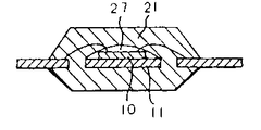
제 1 도는 발포제가 칩소자위에 도포된 상태의 종래 수지밀폐형소자 단면도.1 is a cross-sectional view of a conventional resin sealed device in which a blowing agent is applied onto a chip device.
제 2 도는 칩소자를 둘러싸는 중공부를 갖는 종래 수지밀폐형소자의 단면도.2 is a cross-sectional view of a conventional resin sealed element having a hollow portion surrounding a chip element.
제 3 도는 본 발명의 실시예.3 is an embodiment of the present invention.
제 4 도는 본 발명에 따른 아일렌드부의 제1실시예.4 is a first embodiment of an island portion according to the present invention.
제 5 도는 본 발명에 따른 칩소자위에 발포체가 도포된 상태를 보여주는 단면도.5 is a cross-sectional view showing a state that the foam is applied on the chip element according to the present invention.
제 6 도는 본 발명에 따른 아일렌드부의 제2실시예.6 is a second embodiment of an island portion according to the present invention.
제 7 도는 본 발명에 따른 아일렌드부의 제3실시예.7 is a third embodiment of an island portion according to the present invention.
제 8 도는 본발명에 따른 아일렌드부의 제4실시예.8 is a fourth embodiment of an island portion according to the present invention.
제 9a 도 및 제 9b 도는 본 발명에 따른 다른 실시예의 평면도 및 단면도.9A and 9B are plan and cross-sectional views of another embodiment according to the present invention.
제 10a 도 및 제 10b 도는 본 발명에 따른 또 다른 실시예의 평면도 및 단면도이다.10A and 10B are plan and cross-sectional views of yet another embodiment according to the present invention.
* 도면의 주요부분에 대한 부호의 설명* Explanation of symbols for main parts of the drawings
10,30,60,70,80,90,110,120,130 : 칩소자10,30,60,70,80,90,110,120,130: chip device
11,31,41,51,61,71,111 : 아일렌드부11,31,41,51,61,71,111: island part
12,35,36,65,66,115,116 : 내부리드12,35,36,65,66,115,116: Internal lead
13,33,34,63,73,151,152,154 : 본딩와이어13,33,34,63,73,151,152,154: bonding wire
14,40 : 발포체 27,37,67,77,117 : 중공부14,40
21,38,68,100,150 : 수지패키지 32,42,52,62,72,112 : 측벽부21,38,68,100,150:
31A,41A,51A,75,85,95 : 리드부 32A : 측부31A, 41A, 51A, 75, 85, 95: Lead
39,43,53 : 요홈부 55 :접속부39, 43, 53: groove portion 55: connection portion
69 : 오목부 113,123,133 : 구멍69: recess 113,123,133: hole
112 : PCB 140,141 : 프린트배선112: PCB 140,141: printed wiring
본 발명은 수지밀폐형소자 및 그 제조방법에 관한 것으로, 특히 반도체칩이라던가 표면탄성파소자와 같은 칩소자의 밀봉상태를 유지토록 하기 위한 중공부를 갖춘수지밀폐형소자 및 그 제조 방법에 관한 것이다.BACKGROUND OF THE
일반적으로 표면탄성파소자를 수지물로 밀폐시키는 경우에는 표면탄성피소자의 진동을 허용하는 중공부를 칩소자윗쪽에다 형성시켜 놓는 것이 필요하게 되고, 이에 대해 종래에도 일본국 특허공개 제60-53058호에 중공부를 갖춘 수지밀폐형소자의 구조 및 그 제조방법이 소개되고 있다. 즉, 이는 제 1 도 및 제 2 도에 도시된 바와 같이, 먼저 리드프레임의 아일렌드(11)상에 설치된 보딩와이어(13) 와 내부리드(12)에 접속된 칩소자(10)표면에 에탄올에 희석시킨 발포체(14)를 도포한 다음 에탄올을 휘발시켜 수지밀폐공정을 실행하도록 되어 있는데, 이 밀폐공정에서 발포체(14)를 발포시켜 제2도와 같이 중공부(27)를 칩(10)표면에다 형성시키도록 되어 있다.In general, in the case where the surface acoustic wave element is sealed with a resin material, it is necessary to form a hollow part on the upper side of the chip element to allow vibration of the surface elastic wave element, which is also conventionally disclosed in Japanese Patent Laid-Open No. 60-53058. The structure of a resin sealed element with a part and a manufacturing method thereof have been introduced. That is, as shown in FIGS. 1 and 2, first, ethanol is formed on the surface of the
그리고, 이와 같은 종래의 수지밀폐형소자는 아일렌드부(11)가 평판형으로 되어 있어 돔형중공부를 형성 시키기 위해서는 발포체(14)를 그 표면장력을 이용해서 돔형으로 도포시키고나서 밀폐공정에서 특수온도로 발포체를 팽창시킴으로써, 제2도에 도시된 바와 같이 돔형중공부(27)를 형성시켜 주도록 되어 있다.In the conventional resin-sealed device, the island portion 11 has a flat plate shape, and in order to form the domed hollow portion, the
그런데 상기 아일렌드부(11)에서 칩소자(10)의 면적 비율이 클 경우에는 칩소자(10)위에 충분한 두께의 발포체를 도포시키기가 어렵고, 특히 칩소자(10)의 가장자리 부위에서 중공부(27)가 너무 좁아지게 되는 것이 문제로 되고 있어서, 발포체를 충분한 두께로 유지시켜지도록 하기 위해 발포체의 점도를 증가시켜 주고 있었다.However, when the area ratio of the
그러나 이와 같은 경우에는 본딩와이어가 큰 스트레스를 받게 되어, 스트레스에 의해 본딩와이어의 루프가 손상되게 될 뿐만아니라 때때로 칩소자와 본딩와이어가 접촉되게 되며, 더구나 높은 점성 때문에 칩소자 위에 균일한 두께로 발포체를 도포시키는 것이 곤란해서 원하는 중공부를 형성시키기가 어려웠다. 또 중공부가 불완전해서 내부벽이 칩소자에 접촉하게 되면 신뢰도를 테스트하는 동안 칩소자에 열싸이클이 작용해서 수축되기 때문에 스트레스가 발생하게 되고 , 그 때문에 칩소자가의 열화가 초래되게 되는바, 이런 문제들을 표면탄성파소자 뿐만 아니라 반도체소자와 같은 다른 칩소자들에게도 발생하고 있다.However, in such a case, the bonding wires are subjected to a great stress, and the stress of the bonding wires is not only damaged, but also the chip elements and the bonding wires sometimes come into contact with each other. Moreover, the foam has a uniform thickness on the chip elements due to the high viscosity. It was difficult to apply, which made it difficult to form the desired hollow portion. In addition, if the hollow part is incomplete and the inner wall comes into contact with the chip element, the stress is generated because the thermal cycle acts on the chip element and shrinks during the reliability test, which causes the chip element deterioration. This is happening not only to surface acoustic wave devices but also to other chip elements such as semiconductor devices.
이에 본 발명은 상기과 같은 문제점을 해결하기 위한발명된 것으로, 칩소자에 열스트레스가 가해지지 않도록 칩소자 위에다 큰 중공부를 갖는 수지밀폐형소자 및 그 제조방법을 제공합을 그 목적으로 한다. 이와같은 목적을 달성하기 위한 본 발명 수지밀폐소자는 칩소자와, 이 칩소자를 지지하기 위한 아일렌드부, 상기 칩소자를 부분적으로 둘러싸는 측벽부 및, 상기 칩소자를 밀폐하면서 이 칩소자가 수지패키지와 접촉되지 않도록 분리시켜 주기 위해 상기 측벽부 이내로 중공(中空)을 부분적으로 한정해 주는패키지로 구성된다. 그리고 이상과 같은 수지밀폐형소자를 제조함에는, 특벽부를 갖는 아일렌드부를 준비하는 단계와 상기 측벽부에 의해 부분적으로 칩소자를 둘러싸도록 상기 아일랜드부상에 칩소자를 본댕해 주는 단계, 상자를 둘러싸는 중공부를 형성시키기 위해 임시도포물질을 제거시키는 단계로 이루어지게 된다.Accordingly, the present invention has been made to solve the above problems, and an object thereof is to provide a resin-sealed device having a large hollow portion over the chip device and a method of manufacturing the same so that thermal stress is not applied to the chip device. The resin sealing device of the present invention for achieving the above object comprises a chip element, an island portion for supporting the chip element, a side wall portion partially surrounding the chip element, and the chip element sealing the chip element. It is composed of a package that partially defines the hollow within the side wall portion to separate it from contact with the resin package. In the manufacturing of the resin-sealed device as described above, preparing an island portion having a special wall portion, bonding the chip element on the island portion so as to partially surround the chip element by the side wall portion, surrounding the box The temporary coating material is removed to form the hollow part.
이하 본 발명을 도면을 참조해서 상세히 설명한다.Hereinafter, the present invention will be described in detail with reference to the drawings.
제 3 도는 본 발명의 일실시예가 도시된 단면도로서, 밀폐형소자가 아일렌드부(31)위에 결합된 칩소자(30)인 예컨대 표면탄성소자로 구성되고, 아일렌드부(31)에는 상기 칩소자(30)를 둘러싸도록 그 주변부에 측벽부(32)가 형성됨과 더불어 중공부(37)가 상기 칩소자(30)를 둘러싸도록 되어 있으며, 이 칩소자(30)는 본딩와이어(33,34)를 매개로 내부리드(35,36)와 연결되고, 상기 측벽부(32)는 중공부(37)의 양측부를 이루면서 상기 중공부(37)의 가장자리 부위높이가 아일렌드(31)의표면보다 상대적으로 높도록 되어 수지패키지(38)로부터 칩소자(30)를 분리시키기 위한 충분한 공간이 확보되도록 되어 있다.3 is a cross-sectional view showing an embodiment of the present invention, in which the hermetic element is composed of, for example, a surface elastic element, which is a
한편 제 4 도를 참조해서 본 발명 수지밀폐형소자를 제조하는 과정을 설명하면, 먼저 리드프레임을 준비해서 예컨데 프레스공정으로 측부(32A)를 절곡시켜 측벽부(32)와 아일렌드부(31) 및 패키지(도시되지 않음)안에 아일렌드부(31)를 지지하기 위한 리드부(31A)를 형성하는 바, 이때 리드부(31A)가 형성됨에 따라 요흠부(39)가 형성되게 된다.Meanwhile, referring to FIG. 4, the process of manufacturing the resin-sealed device of the present invention will be described. First, a lead frame is prepared and, for example, the
여기서 측벽부(32)의 높이는 아일렌드부(31)에 결합하는 칩소자(30)의 높이보다 거의 겉거나 보다 조금 높아지게 되는데, 칩소자(30)와 내부리드 사이를 와이어본딩 해 주기 위해서는 내부리드(35,36)표면과 칩소자(30)표면이 일치시켜지도록 리드프레임의 아일렌드부(31)를 낮추어 주는 것이 좋다. 제5도에는 아일렌드부(31)가 낮춰진 실시예가 도시되어져 있다.Here, the height of the
이어 칩소자(30)를 아일렌드부(31)위에 접착시키고나서 와이어본딩을 실시해서 칩소자(30)와 내부리드(35,36)를 접속시킨다. 그리고 적당량의 임시도포물질을 칩소자(30)표면에다 도포하게 되는바, 이 경우에 예를들어 에탄올 또는 왁스, 즉 파라핀과 같은 승화성물질과 함께 희석시킨 발포체(40)가 임시도포물질로 사용된다. 이렇게 에탄올에 희석시킨 발포체를 사용하는 경우에는 다음과 같이 되는바, 즉 요홈부(39)의 폭이 약0.3mm 보다 좁게 되면 표면장력 때문에 요홈부(29)를 통해 발포체(40)의 누출이 방지되고, 발포체(40)의 중앙부가 표면장력에 따라 돔형이 형성되도록 팽창시켜지게 된다. 따라서 발포체가 칩소자(30)의 마운트부에서 충분한 두께로 형성되고, 측벽부(32)의 부근에서는 적어도 이 측벽부(32)높이보다 두꺼운 충분한 두께의 발포체가 형성되게 된다.Subsequently, the
다음 예컨데 이동성형공정을 이용하는 밀폐단계가 약175℃에서 이루지는데, 이 단계에서는 발포체의 발포시점이 성형온도 이하이기 때문에 발포체의 발포가 동시에 이루어지게 되는바, 여기서 에조비스.이소.브티로.니트리드(AIBN:azobis.iso.butryro.nitride)가 발포체로 사용될 때는 발포체의 발포시작온도가 106℃로 된다.For example, a sealing step using a mobile molding process is performed at about 175 ° C. In this step, the foaming is simultaneously performed since the foaming point of the foam is lower than the molding temperature, where ezobis.iso.butti.nit When lead (AIBN: azobis.iso.butryro.nitride) is used as a foam, the foaming start temperature of the foam becomes 106 ° C.
이와 같은 제조방법에서, 임시로 충분한 두께로 칩소자를 도포시켜 놓은 발포체를 제거하게 되면 중공부로 되는 충분한 공간이 얻어지게 됨으로써 표면탄성파소자가 적당히 진동될 수 있게 되고, 더욱이 충분한 두께로 형성되게 됨으로써 점성이 높은 발포체를 사용할 필요가 없게 됨으로, 본딩와이어의 스트레스가 감소되어 본딩와이어의 루프가 양호해지게 된다.In such a manufacturing method, if the foam to which the chip element is temporarily coated is removed, sufficient space to be a hollow part is obtained, so that the surface elastic wave element can be vibrated appropriately, and furthermore, it is formed to have a sufficient thickness. By eliminating the need to use this high foam, the stress of the bonding wire is reduced and the loop of the bonding wire becomes good.
한편 파라핀과 같은 왁스류의 승화성물질이 임시도포물질로 사용되는 경우에는, 승화시작온도가 약60℃가 되므로 중공부가 성형공정에서 형성되게 된다.On the other hand, when a sublimable material such as paraffin wax is used as a temporary coating material, the sublimation start temperature is about 60 ℃ to form a hollow portion in the molding process.
제 6 도는 본 발명에서의 아일렌드부에 대한 제2실시예로서, 측벽부(42)에 다수의 요홈부(43)가 간간히 형성되어져 있는데, 이측벽부(42)는 프레스 공정에서 아일렌드부(41)의 측부를 절곡시켜 형성시킨다. 여기서 프레스로 측벽부(42)를 절곡시키는 단계는 비교적 쉽게 이루어지게 되고, 또 발포체는 중공부가 형성되는 동안 다수의 요홈부(43)를 통해 쉽게 발포되게 된다.6 is a second embodiment of the island in the present invention, a plurality of
제 7 도는 본발명에서의 따른 아일레드부에 대한 제3실시예로서, 요홈부(53)가 측벽부(52)에 형성되면서 이측벽부(52)가 접속부(55)에 접속된 구조로 되어 있는바, 이러한 구조는 측벽부 (52)가 제 6 도에 도시된 실시예에 비해 더욱 견고해 지게 된고, 상기 요홈부(53)를 통하여 칩소자(도시되지 않음)와 내부리드선사이의 와이어본딩이 이루어지게 된다.7 is a third embodiment of the eye red part according to the present invention, in which the recessed
제 8 도는 본 발명에서의 아일렌드부에 대한 제4실시예로서, 오목부(69)가 형성된 오목부(69)가 프레스공정으로 형성시켜짐과 더불어, 측벽부(62)와 칩소자(60)상에 임시도포물질이 충분한 두께로 도포시켜질 수 있도록 되어 있다.8 is a fourth embodiment of the island according to the present invention, wherein the
따라서 중공부(67)의 충분한 공간이 형성되고, 칩소자(60)는 본딩와이어(63,64)를 매개로 내부리드(65,66)에 각각 접속시켜진 다음 수지패키지(68)로 밀폐시켜지게 된다.Therefore, sufficient space of the
또한 본 실시예는 멀티 칩(multi-chip)형 수지밀폐형소자에도 적용시킬 수가 있는바, 이때는 적어도 칩소자의 하나가 중공부로 둘러싸여지도록 하는 것이 필요하게 된다.In addition, the present embodiment can also be applied to a multi-chip resin sealed element, which requires at least one of the chip elements to be surrounded by a hollow portion.
제9a 및 9b 도는 멀티칩형수지밀폐형소자의 실시예가 도시된 것으로, 여기서는 칩소자(70,80,90)들이 밀폐된 구조로 되어 있다.9A and 9B illustrate an embodiment of a multichip resin sealing element, in which the
제 9a 도는 수지밀폐형소자의 평면도로서, 각 칩소자(70,80,90)가 각 아일렌드부의 리드부(75,85,95)상에 결합되어 본딩와이어와 대응되는 내부리드에 접속되게 된다.9A is a plan view of the resin sealing element, in which each
제 9b 도는 제 9a 도의 Ⅱ-Ⅱ선 담면도로서, 칩소자(70)를 지지하게 되는 아일렌드부(71)에 측벽부(72)가 구비되고, 중공부(77)는 칩소자(70)를 둘러싸도록 형성되어져 있다.9B is a sectional view taken along the line II-II of FIG. 9A. The
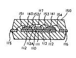
제 10a 도 및 제 10b 도는 본 발명의 또다른 실시예로서 싱글(single) 아일렌드부(111)위에 다수의 칩소자(110,120,130)가 결합된 것인데, 제 10a 도는 수지밀폐형소자의 평면도이고, 제 10b 도는 제 10a 도의 Ⅲ-Ⅲ선 단면도인바, 여기서 다수의 구멍(113,123,133)을 갖는 PCB(112)가 아일렌드부(111)상에 고정되면서 칩소자(110)가 상기 구멍(113)내에 결합되도록 되어 있다. 도면에서 본딩와이어의 도시는 생략하였다. 그리고, 상기 칩소자(110)는 구멍(113) 중심부의 아일렌드부(111)상에 결합되면서 충분한 공간으로 칩소자를 둘러싸는 중공부(117)와 함께 수지패키지(150)로 밀폐시켜져 있다. 또 제 10b 도에 도시된 바와 같이 PCB(112)구멍의 벽부 또는 측벽부는 칩소자를 덮어주게 되고, PCB(112)는 약 0.5mm 두께의 세라믹과 같은 절연재질로 만들어져, 칩소자(110)가 본딩와이어(152,153)와 함께 프린트 배선(140,141)에 접속됨과 더불어 프린트 배선(140,141)과 본딩와이어(151,154)를 매개로 내부리드(115, 116)로 연결되어져 있다.10A and 10B illustrate a plurality of
상기와 같이 본 발명은, 칩소자를 연속적 또는 간간이 둘러싸는 측벽부가 형성시켜짐에 따라 수지킬폐전 소자마운트부상에 승화성물질 등이 안전하고 충분히 도포될 수가 있어서, 수지밀폐시 소자와 수지가 접촉되지 않는 중공구조가 확실하게 형성시켜지게 됨으로써 소자의 특성 및 신뢰성이 향상되게 되고, 또 가령 듀얼 인 라인 패키지(DIP : Dual In-Inc-Packages)라던가 플래트 패키지(FD : Flat packages) 퀴즈 플래트 패키지(QFP : Quad Flat packages) 플라스틱 리드 칩 케리어스(PLC : Plastic Lealed Chip Carriers) 및 싱글 인 라인 패키지 소자(Single In-Line package Levices)와 같은 여러 가지 형태의 수지밀폐형소자에 적용할 수 있게 되는 장점이 있다.As described above, according to the present invention, as the sidewall portion enclosing the chip element is continuously or intermittently formed, a sublimable material or the like can be safely and sufficiently coated on the resin killing element mount portion, so that the resin element contacts with the resin during sealing. As a result, the hollow structure that is not formed is surely formed, thereby improving the characteristics and reliability of the device, and for example, dual in-in-packages (DIP) or flat packages (FD) quiz plate packages ( QFP (Quad Flat packages) The advantages of being applied to various types of resin sealed devices such as Plastic Lealed Chip Carriers (PLC) and Single In-Line package Levices have.
Claims (14)
Applications Claiming Priority (2)
| Application Number | Priority Date | Filing Date | Title |
|---|---|---|---|
| JP62-214319 | 1987-08-28 | ||
| JP62214319A JPS6457739A (en) | 1987-08-28 | 1987-08-28 | Resin seal type element |
Publications (2)
| Publication Number | Publication Date |
|---|---|
| KR890004428A KR890004428A (en) | 1989-04-22 |
| KR910003542B1 true KR910003542B1 (en) | 1991-06-04 |
Family
ID=16653787
Family Applications (1)
| Application Number | Title | Priority Date | Filing Date |
|---|---|---|---|
| KR1019880010738A KR910003542B1 (en) | 1987-08-28 | 1988-08-24 | Resin seal type element and method for manufacturing thereof |
Country Status (3)
| Country | Link |
|---|---|
| US (1) | US4942456A (en) |
| JP (1) | JPS6457739A (en) |
| KR (1) | KR910003542B1 (en) |
Families Citing this family (16)
| Publication number | Priority date | Publication date | Assignee | Title |
|---|---|---|---|---|
| US5847467A (en) * | 1990-08-31 | 1998-12-08 | Texas Instruments Incorporated | Device packaging using heat spreaders and assisted deposition of wire bonds |
| US5605863A (en) * | 1990-08-31 | 1997-02-25 | Texas Instruments Incorporated | Device packaging using heat spreaders and assisted deposition of wire bonds |
| US5278446A (en) * | 1992-07-06 | 1994-01-11 | Motorola, Inc. | Reduced stress plastic package |
| JP3132449B2 (en) * | 1998-01-09 | 2001-02-05 | 日本電気株式会社 | Method of manufacturing resin-encased semiconductor device |
| US5899583A (en) * | 1998-02-09 | 1999-05-04 | Eastman Kodak Company | Viewfinder lens assembly |
| US7778750B2 (en) * | 2002-02-25 | 2010-08-17 | Cummins Inc. | Vehicle communications network adapter |
| US6556782B1 (en) | 2002-08-22 | 2003-04-29 | Eastman Kodak Company | Camera having viewfinder box extending from cover to cover and assembly method |
| JP2008235559A (en) * | 2007-03-20 | 2008-10-02 | Mitsui Chemicals Inc | Hollow package and its manufacturing method |
| US7651891B1 (en) * | 2007-08-09 | 2010-01-26 | National Semiconductor Corporation | Integrated circuit package with stress reduction |
| US8193597B2 (en) * | 2009-11-17 | 2012-06-05 | Avago Technologies Wireless Ip (Singapore) Pte. Ltd. | Acoustic device with low acoustic loss packaging |
| US8232615B2 (en) * | 2010-02-23 | 2012-07-31 | Avago Technologies Wireless Ip (Singapore) Pte. Ltd. | Packaged device with acoustic transducer and amplifier |
| JP6080305B2 (en) * | 2013-08-21 | 2017-02-15 | 新電元工業株式会社 | Semiconductor device manufacturing method, semiconductor device, and lead frame |
| US11211305B2 (en) | 2016-04-01 | 2021-12-28 | Texas Instruments Incorporated | Apparatus and method to support thermal management of semiconductor-based components |
| US10861796B2 (en) * | 2016-05-10 | 2020-12-08 | Texas Instruments Incorporated | Floating die package |
| US10074639B2 (en) | 2016-12-30 | 2018-09-11 | Texas Instruments Incorporated | Isolator integrated circuits with package structure cavity and fabrication methods |
| JP7177330B2 (en) * | 2018-06-28 | 2022-11-24 | 日亜化学工業株式会社 | Method for manufacturing light emitting device |
Family Cites Families (5)
| Publication number | Priority date | Publication date | Assignee | Title |
|---|---|---|---|---|
| US4054901A (en) * | 1975-10-14 | 1977-10-18 | Thermalloy, Inc. | Index mounting unitary heat sink apparatus with apertured base |
| JPS59172253A (en) * | 1983-03-18 | 1984-09-28 | Mitsubishi Electric Corp | Semiconductor device |
| JPS6015955A (en) * | 1983-07-08 | 1985-01-26 | Hitachi Micro Comput Eng Ltd | Semiconductor device |
| JPS6053058A (en) * | 1983-09-02 | 1985-03-26 | Hitachi Ltd | Resin seal type element and manufacture thereof |
| JPS60257546A (en) * | 1984-06-04 | 1985-12-19 | Mitsubishi Electric Corp | Semiconductor device and manufacture thereof |
-
1987
- 1987-08-28 JP JP62214319A patent/JPS6457739A/en active Granted
-
1988
- 1988-08-22 US US07/235,455 patent/US4942456A/en not_active Expired - Fee Related
- 1988-08-24 KR KR1019880010738A patent/KR910003542B1/en not_active IP Right Cessation
Also Published As
| Publication number | Publication date |
|---|---|
| JPH0519310B2 (en) | 1993-03-16 |
| JPS6457739A (en) | 1989-03-06 |
| KR890004428A (en) | 1989-04-22 |
| US4942456A (en) | 1990-07-17 |
Similar Documents
| Publication | Publication Date | Title |
|---|---|---|
| KR910003542B1 (en) | Resin seal type element and method for manufacturing thereof | |
| KR100304681B1 (en) | Mold-bga-type semiconductor device and method for making the same | |
| US8018076B2 (en) | Semiconductor device, semiconductor package for use therein, and manufacturing method thereof | |
| US5275975A (en) | Method of making a relatively flat semiconductor package having a semiconductor chip encapsulated in molded material | |
| US4012766A (en) | Semiconductor package and method of manufacture thereof | |
| KR950025961A (en) | Semiconductor device and manufacturing method | |
| US5646829A (en) | Resin sealing type semiconductor device having fixed inner leads | |
| US5715593A (en) | Method of making plastic-packaged semiconductor integrated circuit | |
| KR20010058583A (en) | Lead End Grid Array Semiconductor package | |
| JP2000133767A (en) | Laminated semiconductor package and its manufacture | |
| US7365439B2 (en) | Semiconductor device, semiconductor package for use therein, and manufacturing method thereof | |
| KR100237051B1 (en) | Bottom lead semiconductor package and method of manufacturing the same | |
| KR20000050486A (en) | Encapsulation method of bga transfer molding in semiconductor | |
| US6858474B1 (en) | Wire bond package and packaging method | |
| KR100237895B1 (en) | Inexpensive resin molded semiconductor device | |
| KR100221918B1 (en) | Chip scale package | |
| JPS5837694B2 (en) | semiconductor equipment | |
| KR100207903B1 (en) | Semiconductor chip package using lead frame having die pad with hole | |
| KR0134168Y1 (en) | Semiconductor package | |
| KR200179421Y1 (en) | Stack semiconductor package | |
| KR100431315B1 (en) | Chip size package fabricated by simple process and fabricating method thereof to reduce manufacturing cost | |
| JPH047865A (en) | Lead frame and semiconductor integrated circuit device using the same | |
| KR900001988B1 (en) | Leadframe for semiconductor device | |
| JPH0547835A (en) | Mounting structure of semiconductor device | |
| KR100282414B1 (en) | bottom leaded-type VCA(Variable Chip-size Applicable) package |
Legal Events
| Date | Code | Title | Description |
|---|---|---|---|
| A201 | Request for examination | ||
| G160 | Decision to publish patent application | ||
| E701 | Decision to grant or registration of patent right | ||
| GRNT | Written decision to grant | ||
| FPAY | Annual fee payment |
Payment date: 20080527 Year of fee payment: 18 |
|
| EXPY | Expiration of term |