KR20220165745A - A single-chip digital pre-distortion (DPD) device implemented using a radio frequency transceiver integrated circuit with integrated DPD function - Google Patents
A single-chip digital pre-distortion (DPD) device implemented using a radio frequency transceiver integrated circuit with integrated DPD function Download PDFInfo
- Publication number
- KR20220165745A KR20220165745A KR1020227035717A KR20227035717A KR20220165745A KR 20220165745 A KR20220165745 A KR 20220165745A KR 1020227035717 A KR1020227035717 A KR 1020227035717A KR 20227035717 A KR20227035717 A KR 20227035717A KR 20220165745 A KR20220165745 A KR 20220165745A
- Authority
- KR
- South Korea
- Prior art keywords
- dpd
- analog
- integrated circuit
- transmit signal
- transceiver
- Prior art date
Links
Images


Classifications
-
- H—ELECTRICITY
- H04—ELECTRIC COMMUNICATION TECHNIQUE
- H04B—TRANSMISSION
- H04B1/00—Details of transmission systems, not covered by a single one of groups H04B3/00 - H04B13/00; Details of transmission systems not characterised by the medium used for transmission
- H04B1/38—Transceivers, i.e. devices in which transmitter and receiver form a structural unit and in which at least one part is used for functions of transmitting and receiving
- H04B1/40—Circuits
-
- H—ELECTRICITY
- H04—ELECTRIC COMMUNICATION TECHNIQUE
- H04B—TRANSMISSION
- H04B1/00—Details of transmission systems, not covered by a single one of groups H04B3/00 - H04B13/00; Details of transmission systems not characterised by the medium used for transmission
- H04B1/02—Transmitters
- H04B1/04—Circuits
- H04B1/0475—Circuits with means for limiting noise, interference or distortion
-
- H—ELECTRICITY
- H04—ELECTRIC COMMUNICATION TECHNIQUE
- H04B—TRANSMISSION
- H04B1/00—Details of transmission systems, not covered by a single one of groups H04B3/00 - H04B13/00; Details of transmission systems not characterised by the medium used for transmission
- H04B1/02—Transmitters
- H04B1/04—Circuits
-
- H—ELECTRICITY
- H04—ELECTRIC COMMUNICATION TECHNIQUE
- H04B—TRANSMISSION
- H04B1/00—Details of transmission systems, not covered by a single one of groups H04B3/00 - H04B13/00; Details of transmission systems not characterised by the medium used for transmission
- H04B1/62—Details of transmission systems, not covered by a single one of groups H04B3/00 - H04B13/00; Details of transmission systems not characterised by the medium used for transmission for providing a predistortion of the signal in the transmitter and corresponding correction in the receiver, e.g. for improving the signal/noise ratio
-
- H—ELECTRICITY
- H04—ELECTRIC COMMUNICATION TECHNIQUE
- H04B—TRANSMISSION
- H04B1/00—Details of transmission systems, not covered by a single one of groups H04B3/00 - H04B13/00; Details of transmission systems not characterised by the medium used for transmission
- H04B1/02—Transmitters
- H04B1/04—Circuits
- H04B2001/0408—Circuits with power amplifiers
- H04B2001/0425—Circuits with power amplifiers with linearisation using predistortion
Landscapes
- Engineering & Computer Science (AREA)
- Computer Networks & Wireless Communication (AREA)
- Signal Processing (AREA)
- Transceivers (AREA)
- Amplifiers (AREA)
Abstract
일 실시예는 디지털 사전 왜곡(DPD) 기능을 포함하지 않는 비-DPD RF 트랜스시버 회로 및 DPD 기능을 포함하는 DPD RF 트랜스시버 집적 회로를 포함하는 시스템에 관한 것이다. 비-DPD RF 트랜스시버 회로에 의해 출력되는 제1 아날로그 RF 송신 신호는, 수신 신호 경로에 의해 생성된 수신 베이스밴드 데이터는 제1 아날로그 RF 송신 신호를 나타내도록 DPD RF 트랜스시버 집적 회로의 수신 신호 경로에 의해 수신된다. DPD RF 트랜스시버 집적 회로에 의해 생성된 수신 베이스밴드 데이터는 DPD RF 트랜스시버 집적 회로의 송신 신호 경로에 의해 수신된다. 송신 신호 경로에 의해 출력되는 제2 아날로그 RF 송신 신호는 전력 증폭기에 의한 증폭을 위한 제1 아날로그 RF 송신 신호의 디지털 방식으로 사전 왜곡된 버전이다.One embodiment is directed to a system that includes a non-DPD RF transceiver circuit that does not include digital predistortion (DPD) functionality and a DPD RF transceiver integrated circuit that includes DPD functionality. The first analog RF transmit signal output by the non-DPD RF transceiver circuit is transmitted by the receive signal path of the DPD RF transceiver integrated circuit such that receive baseband data generated by the receive signal path represents the first analog RF transmit signal. Received. Receive baseband data generated by the DPD RF transceiver integrated circuit is received by a transmit signal path of the DPD RF transceiver integrated circuit. The second analog RF transmit signal output by the transmit signal path is a digitally pre-distorted version of the first analog RF transmit signal for amplification by the power amplifier.

Description
관련 출원에 대한 상호 참조CROSS REFERENCES TO RELATED APPLICATIONS
본 출원은 2020년 3월 18일에 출원된 미국 특허 가출원 제62/991,277호의 이익을 주장하며, 이는 그 전체가 참조로서 본원에 포함된다.This application claims the benefit of US Provisional Patent Application No. 62/991,277, filed March 18, 2020, which is incorporated herein by reference in its entirety.
기지국("액세스 지점"으로도 지칭됨)은 무선 주파수 신호를 적어도 하나의 다른 디바이스와 무선으로 송수신한다. 통상적으로, 송신된 신호는 선형 증폭기를 사용하여 증폭된다. 기지국 내에서 또는 이와 함께 사용하기 위해 증폭기를 선형화하는 많은 방법이 있다.A base station (also referred to as an “access point”) wirelessly sends and receives radio frequency signals to and from at least one other device. Typically, the transmitted signal is amplified using a linear amplifier. There are many ways to linearize an amplifier for use within or with a base station.
증폭기를 선형화하는 하나의 접근법은 송신될 신호를 디지털 방식으로 사전 왜곡한다. 증폭기의 비선형 전달 특성의 역 모델이 개발되었다. 송신 신호는 아날로그 신호로 변환하고 증폭기를 사용하여 증폭하기 전에 송신 신호의 디지털 버전에 역 모델을 적용하여 디지털 방식으로 사전 왜곡된다. 송신 신호의 디지털 버전에 역 모델을 적용하면, 결과적인 최종 증폭된 신호가 왜곡되지 않은 것으로 나타나도록 증폭 동안 도입된 왜곡과 동일하거나 반대가 되도록 의도된 방식으로 송신 신호를 사전 왜곡한다.One approach to linearizing an amplifier is to digitally pre-distort the signal to be transmitted. An inverse model of the nonlinear transfer characteristics of the amplifier was developed. The transmit signal is digitally predistorted by applying an inverse model to the digital version of the transmit signal before converting it to an analog signal and amplifying it using an amplifier. Applying an inverse model to the digital version of the transmit signal predistorts the transmit signal in an intended manner to equal or reverse the distortion introduced during amplification so that the resulting final amplified signal appears undistorted.
증폭기에 의해 야기되는 왜곡에 대한 이러한 보상은, 증폭기가 높은 출력 레벨(즉, 포화에 가까운)로 작동될 때 특히 필요하다. 높은 출력 레벨에서 증폭기를 작동시키는 것은 통상적으로 더 높은 효율과 더 낮은 비용을 제공한다.Such compensation for the distortion caused by the amplifier is particularly necessary when the amplifier is operated at high output levels (ie close to saturation). Operating the amplifier at high output levels typically provides higher efficiency and lower cost.
증폭기의 전달 특성의 변화를 설명하기 위해, 디지털 사전 왜곡(DPD)에 사용된 역 모델이 증폭기의 입력 및 출력 신호의 실시간 비교에 기초하여 업데이트된다. 이러한 비교를 하기 위해, 증폭기에 의해 출력된 아날로그 무선 주파수(RF) 출력 신호를 측정한다.To account for changes in the transfer characteristics of an amplifier, the inverse model used for digital predistortion (DPD) is updated based on a real-time comparison of the amplifier's input and output signals. To make this comparison, measure the analog radio frequency (RF) output signal output by the amplifier.
DPD를 구현하는 이러한 접근법의 단점은 DPD 기능을 구현하는 데 사용되는 처리 디바이스의 높은 가격 및 전력 소비, 사전 왜곡된 송신 신호를 증폭기용 아날로그 입력 신호로 변환하는 데 사용되는 디지털-아날로그 변환기, 및 증폭기에 의해 생성된 출력 신호의 버전을 디지털화하는 데 사용되는 아날로그-디지털 변환기이다. 이들 단점은 증폭기의 전체 효율을 감소시킨다. 이러한 단점을 감소시키고 결과적인 증폭기의 효율을 개선하기 위해, 일부 집적 회로 공급업체는 이러한 DPD 기능을 기지국에서 사용되는 RF 트랜스시버 칩셋에 통합하였다. 즉, 사전 왜곡된 디지털 송신 신호를 생성하는 DPD 처리, 사전 왜곡된 디지털 송신 신호를 증폭기의 아날로그 입력 신호로 변환하는 디지털-아날로그 변환기, 및 증폭기에 의해 생성된 출력 신호의 버전을 디지털화하는 아날로그-디지털 변환기는 전력 효율적인 ASIC(application-specific integrated circuit) 기술을 사용하여 구축된 단일 집적 회로에 모두 통합된다.Disadvantages of this approach to implementing DPD include the high price and power consumption of the processing device used to implement the DPD function, the digital-to-analog converter used to convert the pre-distorted transmit signal to an analog input signal for the amplifier, and the amplifier. It is an analog-to-digital converter used to digitize the version of the output signal produced by These drawbacks reduce the overall efficiency of the amplifier. To alleviate these drawbacks and improve the efficiency of the resulting amplifier, some integrated circuit vendors have integrated these DPD functions into RF transceiver chipsets used in base stations. That is, DPD processing to create a pre-distorted digital transmit signal, a digital-to-analog converter to convert the pre-distorted digital transmit signal to an analog input signal of the amplifier, and an analog-to-digital converter to digitize the version of the output signal produced by the amplifier. The converter is all integrated into a single integrated circuit built using power-efficient application-specific integrated circuit (ASIC) technology.
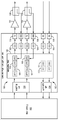
통합 DPD 기능을 갖는 이러한 RF 트랜스시버 집적 회로(100)의 일례가 도 1에 도시된다. 2-채널 RF 트랜스시버 집적 회로(100)이 도 1에 도시된다. RF 트랜스시버 집적 회로(100)는 2개의 송신 신호를 송신하고 2개의 수신 신호를 수신할 수 있다(예: 2x2 MIMO(multiple-input-multiple-output) 무선 채널에 사용되는 2개의 송신 및 2개의 수신 스트림). 도 1에 도시된 바와 같이, RF 트랜스시버 집적 회로(100)에 의해 처리되는 송수신 신호에 대한 베이스밴드 처리는 외부 처리 디바이스(102)(예: FPGA(field-programmable gate array) 또는 DSP(digital signal processor))에 의해 수행된다.An example of such an RF transceiver integrated circuit 100 with integrated DPD functionality is shown in FIG. 1 . A two-channel RF transceiver integrated circuit 100 is shown in FIG. The RF transceiver integrated circuit 100 may transmit two transmit signals and receive two receive signals (e.g., two transmit and two receive signals used for a 2x2 multiple-input-multiple-output (MIMO) radio channel. stream). As shown in FIG. 1, the baseband processing of the transmission and reception signals processed by the RF transceiver integrated circuit 100 is performed by an external processing device 102 (eg, a field-programmable gate array (FPGA) or a digital signal processor (DSP)). )) is performed by
RF 트랜스시버 집적 회로(100)는 RF 트랜스시버 집적 회로(100)를 외부 처리 디바이스(102)에 결합하도록 설정된 직렬 인터페이스(104)를 포함한다. 도 1에 도시된 실시예에서, 직렬 인터페이스(104)는 JEDEC(Joint Electron Device Engineering Council)에 의해 공포된 JESD204B 표준을 지원한다. 이러한 직렬 인터페이스(104)는 또한 본원에서 "JESD204B 인터페이스"(104)로 지칭된다. 도 1에 도시된 예는 직렬 인터페이스(및 보다 구체적으로 JESD204B 인터페이스)를 사용하여 구현되는 것으로 본원에서 설명되지만, RF 트랜스시버 집적 회로(100)는 다른 유형 또는 다수의 직렬 또는 병렬 인터페이스를 사용하여 외부 처리 디바이스(102)에 결합될 수 있다는 것을 이해해야 한다. 예를 들어, 하나의 대안적인 예에서, 다수의 병렬 고속 인터페이스가 사용될 수 있으며, 여기서 각각의 송신 채널 및 각각의 수신 채널에 대해 별도의 병렬 고속 인터페이스가 제공된다.The RF transceiver integrated circuit 100 includes a
도 1에 도시된 예에서, 송신 신호 경로(103)에서, 두 송신 채널에 대한 송신 베이스밴드 데이터는 JESD204B 인터페이스(104) 중 하나를 통해 처리 디바이스(102)로부터 공급된다(여기서, 이 인터페이스(104)는 또한 "송신" 직렬 인터페이스(104) 또는 "송신 JESD204B 인터페이스(104)로 지칭됨). 각각의 송신 채널에 대한 송신 베이스밴드 데이터는 다른 방식으로 처리 디바이스(102)로부터 공급될 수 있다(예: 다수의 병렬 고속 인터페이스를 사용하여 RF 트랜스시버 집적 회로(100)를 외부 처리 디바이스(102)에 결합하는 경우, 각각의 송신 채널에 대한 별도의 병렬 고속 인터페이스를 사용함). RF 트랜스시버 집적 회로(100)는 각 채널에 대한 송수신 베이스밴드 데이터를 처리하는 베이스밴드 처리 모듈(106)을 포함한다. 도 1에 도시된 예에서, 베이스밴드 처리 모듈(106)은 DPD 기능(108) 및 CFR(crest factor reduction) 기능(110)을 구현하여, 송신 데이터밴드 데이터에 대해 DPD 및 CFR을 각각 수행함으로써 각 채널에 대한 해당 송신 베이스밴드 데이터를 처리한다. 베이스밴드 처리 모듈(106)은 송신 신호 경로의 경우 iFFT(inverse fast Fourier transform) 처리(107) 및/또는 DUC(digital up conversion)(109), 또는 수신 신호 경로의 경우 DDC(digital down conversion)(111) 및/또는 FFT(fast Fourier transform) 처리(113)와 같은 다른 유형의 처리를 또한 구현할 수 있음을 이해해야 한다.In the example shown in FIG. 1, on
송신 신호 경로(103)에서, RF 트랜스시버 집적 회로(100)는 RF 트랜스시버 집적 회로(100)에 의해 지원되는 2개의 채널 각각에 대한 각각의 디지털-아날로그 변환(DAC) 모듈(112)를 포함한다. 임의의 종래의 DAC 디바이스는 DAC 모듈(112)을 구현하는 데 사용될 수 있다(예: 실제 중간 주파수(IF) 아날로그 신호를 출력하는 DAC 디바이스, 복잡한 IF 아날로그 신호를 출력하는 DAC 디바이스, 또는 RF 아날로그 신호를 직접 출력하는 DAC 디바이스). 각각의 채널에 대해 결과적인 처리된 송신 베이스밴드 데이터는 각각의 디지털-아날로그 변환 모듈(112)로 출력된다. 각각의 디지털-아날로그 변환 모듈(112)은 송신 베이스밴드 데이터를 아날로그 신호로 변환하고, (필요한 경우) 직교 변조하고, (필요한 경우) 아날로그 신호를 원하는 RF 주파수로 상향 변환하고, 상향 변환된 RF 신호를 필터링하고, RF 트랜스시버 집적 회로(100) 내에 포함된 각각의 아날로그 송신(TX) 포트(114) 상에 필터링된 RF 신호를 출력하도록 설정된다. 각각의 송신 포트(114)는, 외부 안테나(미도시)를 통한 무선 송신용 해당 송신 포트(114) 상에서 출력되는 각각의 아날로그 송신 RF 신호를 증폭하는, 각각의 외부 전력 증폭기(116)에 결합된다.In the
수신 신호 경로(105)에서, RF 트랜스시버 집적 회로(100)는 RF 트랜스시버 집적 회로(100)에 의해 지원되는 2개의 채널 각각에 대한 아날로그-디지털 변환(ADC) 모듈(118)을 포함한다. 외부 안테나(미도시)를 통해 수신된 아날로그 RF 신호는 RF 트랜스시버 집적 회로(100) 내에 포함된 수신(RX) 포트(120)을 통해 입력된다. 아날로그 RF 수신 신호는 수신 포트(120)를 통해 입력되기 전에 (예를 들어, 적절한 외부 저 노이즈 증폭기(LNA)(미도시)를 사용하여) 증폭되고 (예를 들어, 적절한 외부 밴드-패스 필터(미도시)를 사용하여) 필터링될 수 있다.In the
각각의 아날로그-디지털 변환 모듈(118)은 아날로그 RF 수신 신호를 수신 베이스밴드 데이터로 변환하고 베이스밴드 처리 모듈(106)에 의한 베이스밴드 처리를 위해 이를 출력하도록 설정된다. 수신 신호 경로(105)에서, 베이스밴드 처리 모듈(106)은, JESD204B 인터페이스(104)(이 인터페이스(104)는 또한 여기에서 "수신" 직렬 인터페이스(104) 또는 "수신" JESD204B 인터페이스(104)로 지칭됨) 중 하나를 통해 결과적인 수신 베이스밴드 데이터를 처리 디바이스(102)에 출력하도록 설정된다.Each analog-to-
도 1에 도시된 예에서, RF 트랜스시버 집적 회로(100)에 의해 지원되는 2개의 채널 각각에 대해, RF 트랜스시버 집적 회로(100)는 2개의 채널 각각에 대한 각각의 관찰 아날로그-디지털 변환(ADC) 모듈(124)에 결합된 각각의 관찰 수신 포트(122)를 포함한다. 각각의 외부 RF 결합기(126)는 각각의 채널에 대한 각각의 외부 전력 증폭기(116)의 출력에 결합된다. 각각의 RF 결합기(126)은 연관된 전력 증폭기(116)에 의해 출력되는 아날로그 RF 출력 신호의 버전인 결합 신호를 출력한다. 각각의 RF 결합기(126)에 의해 출력되는 결합 신호는 각각의 관찰 수신(OBS) 포트(122)를 통해 RF 트랜스시버 집적 회로(100)에 의해 수신된다. 각각의 관찰 아날로그-디지털 변환(ADC) 모듈(124)은, 상응하는 관찰 수신 포트(122)를 통해 수신된 상응하는 아날로그 결합 RF 신호를 디지털 베이스밴드 데이터로 변환하도록 설정된다. 각각의 수신된 결합 신호에 대한 베이스밴드 데이터는 베이스밴드 처리 모듈(106)에 의한 베이스밴드 처리를 위해 출력된다. 보다 구체적으로, 각각의 수신된 결합 신호에 대한 베이스밴드 데이터는 DPD 기능(108)에 의해 사용되어 해당 채널에 대한 송신 베이스밴드 데이터 상에서 DPD를 수행하는 데 사용되는 역 모델을 업데이트한다. 상술된 바와 같이, 상응하는 전력 증폭기(116)의 비선형 전달 특성의 역 모델은 상응하는 전력 증폭기(116)의 전달 특성의 변화를 고려하기 위해 업데이트된다. 역 모델은 상응하는 전력 증폭기의 입력 및 출력 신호의 실시간 비교에 기초하여 업데이트된다. 상응하는 전력 증폭기(116)의 비선형 전달 특성의 역 모델을 구현하는 데 사용되는 계수는, (아날로그 신호로 변환 후에, 상응하는 전력 증폭기(116)에 입력되는) 송신 신호의 사전 왜곡된 디지털 버전과 (상응하는 전력 증폭기(116)의 출력의 버전인) 디지털 결합 신호 사이의 차이에 기초하여 업데이트된다.In the example shown in FIG. 1, for each of the two channels supported by the RF transceiver integrated circuit 100, the RF transceiver integrated circuit 100 performs a respective observed analog-to-digital conversion (ADC) for each of the two channels. Each
OBS 수신기 아키텍처는 다른 방식으로 구현될 수 있음을 이해해야 한다. 예를 들어, 공유 OBS 수신기 아키텍처가 사용될 수 있다. 하나의 이러한 예에서, 단일 OBS 포트(122) 및 관찰 ADC 모듈(124)은 2개의 상응하는 RF 결합기(126)의 출력과 OBS 포트(122) 사이에 RF 스위치를 포함함으로써 두 개의 송신 채널과 함께 사용하기 위해 제공될 수 있으며, 여기서 RF 스위치는 어느 송신 채널이 관찰되고 있는지 결정하기 위해 제어된다. 공유 OBS 수신기 아키텍처의 다른 예에서, 단일 관찰 ADC 모듈(124)은, 2개의 OBS 포트(122)와 단일 ADC 모듈(124)의 입력 사이에 RF 스위치를 포함함으로써, 송신 채널과 함께 사용 및 2개의 OBS 포트(122)와 함께 사용하기 위해 제공될 수 있으며, 여기서 RF 스위치는 어떤 송신 채널이 관찰되고 있는지 결정하기 위해 제어된다.It should be understood that the OBS receiver architecture may be implemented in different ways. For example, a shared OBS receiver architecture may be used. In one such example, a
"베이스밴드 데이터"라는 어구는 베이스밴드 처리 모듈(106)에 의해 DAC 모듈(112)로 출력되는 디지털 데이터 및 ADC 모듈(118 및 124)에 의해 베이스밴드 처리 모듈(106)로 출력되는 디지털 데이터를 지칭하기 위해 사용되지만, 이러한 데이터는 DAC 모듈(112), ADC 모듈(118 및 124), 및 베이스밴드 처리 모듈(106)이 구현되는 방법에 적절한 형태로 출력되는 것을 이해해야 한다. 또한, 베이스밴드 데이터가 베이스밴드 처리 모듈(106)에 의해 DAC 모듈(112)로 출력되는 형태는, 디지털 데이터가 ADC 모듈(118 및 124)에 의해 베이스밴드 처리 모듈(106)로 출력되는 형태와 상이할 수 있다.The phrase "baseband data" refers to digital data output by the
도 1에 도시된 유형의 통합 DPD 기능을 갖는 RF 트랜스시버 집적 회로는 통상적으로, 송신 신호 경로는 상응하는 안테나 및 전력 증폭기를 통해 무선으로 송신되는 아날로그 송신 신호를 생성하는 데 사용되고, 수신 신호 경로는 상응하는 안테나 및 저-노이즈 증폭기를 통해 무선으로 수신되는 아날로그 수신 신호를 수신하는 데 사용되는 기지국에서 사용되도록 설계된다.An RF transceiver integrated circuit with integrated DPD function of the type shown in FIG. 1 is typically used to generate an analog transmit signal that is transmitted wirelessly through a corresponding antenna and power amplifier, and a receive signal path corresponding to the transmit signal path. It is designed for use in base stations used to receive analog reception signals that are received over the air through an antenna and low-noise amplifier.
일 실시예는 제1 아날로그 무선 주파수(RF) 송신 신호 및 전력 증폭기에 대한 디지털 사전 왜곡(DPD)을 수행하는 시스템에 관한 것이다. 시스템은 DPD 기능을 포함하지 않는 비-DPD RF 트랜스시버 회로를 포함한다. 비-DPD RF 트랜스시버 회로는 제1 아날로그 RF 송신 신호를 출력하도록 설정된다. 시스템은 송신 베이스밴드 데이터 입력으로부터 발생된 제2 아날로그 RF 송신 신호를 송신 신호 경로에 출력하도록 설정된 송신 신호 경로를 포함하는 DPD RF 트랜스시버 집적 회로를 더 포함한다. 송신 신호 패치는 통합 DPD 기능을 포함한다. DPD RF 트랜스시버 집적 회로는 아날로그 RF 수신 신호 입력으로부터 생성된 수신 베이스밴드 데이터를 수신 신호 경로에 출력하도록 설정된 수신 신호 경로를 더 포함한다. 시스템은, 수신 신호 경로에 의해 생성된 수신 베이스밴드 데이터는 제1 아날로그 RF 송신 신호를 나타내도록 비-DPD RF 트랜스시버 회로에 의해 출력되는 제1 아날로그 RF 송신 신호가 DPD RF 트랜스시버 집적 회로의 수신 신호 경로에 의해 수신되게 설정된다. 시스템은 DPD RF 트랜스시버 집적 회로에 의해 생성된 수신 베이스밴드 데이터가 DPD RF 트랜스시버 집적 회로의 송신 신호 경로에 의해 수신되도록 설정된다. 송신 신호 경로에 의해 출력되는 제2 아날로그 RF 송신 신호는 전력 증폭기에 의한 증폭을 위한 제1 아날로그 RF 송신 신호의 디지털 방식으로 사전 왜곡된 버전이다.One embodiment relates to a system that performs digital predistortion (DPD) on a first analog radio frequency (RF) transmit signal and a power amplifier. The system includes non-DPD RF transceiver circuitry that does not include DPD functionality. A non-DPD RF transceiver circuit is configured to output a first analog RF transmit signal. The system further includes a DPD RF transceiver integrated circuit including a transmit signal path configured to output a second analog RF transmit signal generated from the transmit baseband data input to the transmit signal path. The transmit signal patch includes an integrated DPD function. The DPD RF transceiver integrated circuit further includes a receive signal path configured to output receive baseband data generated from the analog RF receive signal input to the receive signal path. The system is configured such that a first analog RF transmit signal output by a non-DPD RF transceiver circuit is sent to a receive signal path of the DPD RF transceiver integrated circuit such that receive baseband data generated by the receive signal path represents the first analog RF transmit signal. is set to be received by The system is configured such that receive baseband data generated by the DPD RF transceiver integrated circuit is received by a transmit signal path of the DPD RF transceiver integrated circuit. The second analog RF transmit signal output by the transmit signal path is a digitally pre-distorted version of the first analog RF transmit signal for amplification by the power amplifier.
다른 실시예는 제1 아날로그 무선 주파수(RF) 송신 신호 및 전력 증폭기에 대한 디지털 사전 왜곡(DPD)을 수행하는 방법에 관한 것이다. 상기 방법은, 통합 DPD 기능을 포함하는 DPD RF 트랜스시버 집적 회로의 수신 신호 경로에 의해, DPD 기능을 포함하지 않는 비-DPD RF 트랜스시버 회로에 의해 출력되는 제1 아날로그 RF 송신 신호를 수신하는 단계를 포함한다. 상기 방법은, DPD RF 트랜스시버 집적 회로에 의해, 제1 아날로그 RF 송신 신호를 나타내는 수신 베이스밴드 데이터를 생성하는 단계, DPD RF 트랜스시버 집적 회로의 송신 신호 경로에 의해 수신 베이스밴드 데이터를 수신하는 단계, 및 송신 신호 경로에 의해, 송신 베이스밴드 데이터로부터 생성된 제2 아날로그 RF 송신 신호를 생성 및 출력하는 단계를 더 포함한다. 송신 신호 경로에 의해 출력되는 제2 아날로그 RF 송신 신호는 전력 증폭기에 의한 증폭을 위한 제1 아날로그 RF 송신 신호의 디지털 방식으로 사전 왜곡된 버전이다.Another embodiment relates to a method of performing digital predistortion (DPD) on a first analog radio frequency (RF) transmit signal and a power amplifier. The method includes receiving, by a receive signal path of a DPD RF transceiver integrated circuit that includes integrated DPD functionality, a first analog RF transmit signal output by a non-DPD RF transceiver circuit that does not include DPD functionality. do. The method includes generating, by a DPD RF transceiver integrated circuit, receive baseband data representative of a first analog RF transmit signal; receiving, by a transmit signal path of the DPD RF transceiver integrated circuit, receive baseband data; and and generating and outputting, by the transmit signal path, a second analog RF transmit signal generated from the transmit baseband data. The second analog RF transmit signal output by the transmit signal path is a digitally pre-distorted version of the first analog RF transmit signal for amplification by the power amplifier.
다른 실시예가 개시된다.Another embodiment is disclosed.
다양한 실시예의 세부 사항은 첨부된 도면 및 아래의 설명에 제시되어 있다. 다른 특징 및 장점은 설명, 도면 및 청구범위로부터 명백해질 것이다.The details of various embodiments are set forth in the accompanying drawings and the description below. Other features and advantages will become apparent from the description, drawings and claims.
도 1은 통합 디지털 사전 왜곡(DPD) 기능을 갖는 무선 주파수(RF) 트랜스시버 집적 회로의 일례를 도시하는 블록도이다.
도 2는 통합 DPD 기능을 갖는 RF 트랜스시버 집적 회로가 어떻게 하나의 시스템에서 다른 RF 트랜스시버와 함께 사용될 수 있는지의 예시적인 일 실시예를 도시하는 블록도이다.
도 3은 제1 아날로그 RF 송신 신호 및 전력 증폭기에 대한 디지털 사전 왜곡을 수행하는 방법의 예시적인 일 실시예를 도시하는 상위-레벨 흐름도를 포함한다.
도 4는 통합 DPD 기능을 갖는 RF 트랜스시버 집적 회로가, 다른 RF 트랜스시버에 대한 DPD 기능을 구현하기 위해 DPD 기능을 포함하지 않는 RF 트랜스시버와 함께 사용되는 중계기 시스템의 예시적인 일 실시예를 도시하는 블록도이다.
도 5a는 통합 DPD 기능을 갖는 RF 트랜스시버 집적 회로가, 다른 RF 트랜스시버에 대한 DPD 기능을 구현하기 위해 DPD 기능을 포함하지 않는 RF 트랜스시버와 함께 사용되는 중계기 시스템의 다른 예시적인 실시예를 도시하는 블록도이다.
도 5b는 도 5a와 관련하여 상술된 유형의 DAS에서 사용하기에 적합한 원격 안테나 유닛의 일례를 도시한다.
다양한 도면에서의 유사한 참조 번호 및 명칭은 유사한 요소를 나타낸다.1 is a block diagram illustrating an example of a radio frequency (RF) transceiver integrated circuit with integrated digital pre-distortion (DPD) functionality.
2 is a block diagram illustrating one exemplary embodiment of how an RF transceiver integrated circuit with integrated DPD functionality can be used with other RF transceivers in a system.
3 includes a high-level flow diagram illustrating one exemplary embodiment of a method of performing digital predistortion on a first analog RF transmit signal and a power amplifier.
4 is a block diagram illustrating one exemplary embodiment of a repeater system in which an RF transceiver integrated circuit with integrated DPD functionality is used in conjunction with an RF transceiver that does not include DPD functionality to implement DPD functionality for another RF transceiver. to be.
5A is a block diagram illustrating another exemplary embodiment of a repeater system in which an RF transceiver integrated circuit with integrated DPD functionality is used in conjunction with an RF transceiver that does not include DPD functionality to implement DPD functionality for other RF transceivers. to be.
FIG. 5b shows an example of a remote antenna unit suitable for use in a DAS of the type described above with respect to FIG. 5a.
Like reference numbers and designations in the various drawings indicate like elements.
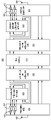
도 2는 어떻게 하나의 시스템(200)에서 통합 디지털 사전 왜곡(DPD) 기능(108)을 갖는 RF 트랜스시버 집적 회로(100)가 다른 RF 트랜스시버(202)에 대한 DPD 기능을 쉽게 구현하기 위해 해당 다른 RF 트랜스시버(202)(예: 그 자체가 DPD 기능을 포함하지 않는 것)와 함께 사용될 수 있는지의 예시적인 일 실시예를 도시하는 블록도이다. 통합 DPD 기능(108)을 갖는 RF 트랜스시버 집적 회로(100)은 또한 여기에서 "DPD" RF 트랜스시버 집적 회로(100)로 지칭되고, 다른 RF 트랜스시버(202)는 또한 여기에서 "비-DPD" RF 트랜스시버(202)로 지칭된다.2 shows how an RF transceiver integrated circuit 100 having an integrated digital pre-distortion (DPD) function 108 in one
도 2에 도시된 실시예에서, DPD RF 트랜시버 집적 회로(100)는 도 1과 관련하여 상술된 RF 트랜시버 집적 회로(100)를 사용하여 구현된다. 도 1에 사용된 동일한 참조 번호는 또한 DPD RF 트랜스시버 집적 회로(100)의 동일한 항목을 지칭하기 위해 도 2에서 사용되며, 그 설명은 간결함을 위해 일반적으로 여기에서 반복되지 않는다. 도 1과 관련하여 상술된 다양한 대안적인 예 및 구현의 설명은 또한 일반적으로 도 2에 도시된 실시예에 적용된다는 것을 이해해야 한다.In the embodiment shown in FIG. 2 , the DPD RF transceiver integrated circuit 100 is implemented using the RF transceiver integrated circuit 100 described above with respect to FIG. 1 . The same reference numbers used in FIG. 1 are also used in FIG. 2 to refer to like items of the DPD RF transceiver integrated circuit 100, and the description is not generally repeated herein for brevity. It should be understood that the descriptions of various alternative examples and implementations discussed above with respect to FIG. 1 also apply generally to the embodiment shown in FIG. 2 .
상술된 바와 같이, DPD RF 트랜스시버 집적 회로(100)는 도 1과 관련하여 상술된 바와 같이 기지국에서 사용하도록 설계된다. 즉, DPD RF 트랜스시버 집적 회로(100)는, 각각의 채널에 대해, 각각의 송신 베이스밴드 데이터를 외부 처리 디바이스로부터 그의 송신 JESD204B 인터페이스(104)를 통해 수신하고, 각각의 송신 베이스밴드 데이터를 사용하여 그의 송신 포트(114) 중 하나를 통해 출력하는 해당 채널에 대해 디지털 방식으로 사전 왜곡된 아날로그 RF 송신 신호를 생성하도록 설계된다. 또한, 상술된 바와 같이, DPD RF 트랜스시버 집적 회로(100)는, 각각의 채널에 대해, 각각의 아날로그 RF 수신 신호를 수신 포트(120) 중 하나를 통해 수신하고, 수신된 아날로그 RF 수신 신호를 사용하여 수신 JESD204B 인터페이스(104)를 통해 외부 처리 디바이스에 출력하는 해당 채널에 대한 수신 베이스밴드 데이터를 생성하도록 설계된다.As discussed above, the DPD RF transceiver integrated circuit 100 is designed for use in a base station as described above with respect to FIG. That is, the DPD RF transceiver integrated circuit 100 receives, for each channel, each transmit baseband data from an external processing device via its transmit
그러나, 도 2에 도시된 실시예에서, DPD RF 트랜스시버 집적 회로(100)는 설계된 방식으로 사용되지 않는다. 이 실시예에서, 비-DPD RF 트랜스시버(202) 내의 송신 신호 경로(204) 및 수신 신호 경로(206)는 아날로그 RF 송수신 신호에 대한 "정상" 송수신 처리를 수행하는 반면, DPD RF 트랜스시버 집적 회로(100)의 송수신 신호 경로(103 및 105)는 비-DPD RF 트랜스시버(202)의 송신 신호 경로(204)에 의해 출력된 아날로그 RF 송신 신호에 대한 DPD를 수행하는 데 사용된다.However, in the embodiment shown in Figure 2, the DPD RF transceiver integrated circuit 100 is not used in the way it was designed. In this embodiment, the transmit
보다 구체적으로, DPD RF 트랜스시버 집적 회로(100)를 그것이 설계된 방식으로 사용하는 대신에, DPD RF 트랜스시버 집적 회로(100)의 각각의 채널에 대해, 비-DPD RF 트랜스시버(202) 내의 송신 신호 경로(204)는 각각의 전력 증폭기(208)에 그렇지 않으면 직접 공급될 수 있는 각각의 아날로그 송신 RF 신호(여기에서 "제1 아날로그 RF 송신 신호"로도 지칭됨)를 생성한다. 전력 증폭기(208)에 직접 공급되는 대신에, 각 채널에 대한 비-DPD RF 트랜스시버(202)의 송신 신호 경로(204)에 의해 생성되고 출력되는 제1 아날로그 송신 RF 신호는 DPD RF 트랜스시버 집적 회로(100)의 수신(RX) 포트(120) 중 각각의 하나 상에서 DPD RF 트랜스시버 집적 회로(100)에 공급된다. 각각의 채널에 대해, DPD RF 트랜스시버 집적 회로(100)의 수신 신호 경로(105)는 베이스밴드 데이터를 생성한다. 도 2에 도시된 실시예에서, 각각의 채널에 대해, 해당 채널에 대해 비-DPD RF 트랜스시버(202)에 의해 생성되고 출력되는 제1 아날로그 송신 RF 신호는 DPD RF 트랜스시버 집적 회로(100) 내에 포함된 각각의 아날로그-디지털 변환(ADC) 모듈(118)에 의해 베이스밴드 데이터로 변환된다. 결과적인 베이스밴드 데이터는 베이스밴드 처리를 위해 DPD RF 트랜스시버 집적 회로(100) 내의 베이스밴드 처리 모듈(106)에 공급된다. DPD RF 트랜스시버 집적 회로(100) 내의 베이스밴드 처리 모듈(106)은, 그것이 수신 JESD204B 인터페이스(104) 상에서 출력될 수 있도록 베이스밴드 데이터를 처리하도록 설정된다.More specifically, instead of using the DPD RF transceiver integrated circuit 100 in the way it was designed, for each channel of the DPD RF transceiver integrated circuit 100, the transmit signal path within the non-DPD RF transceiver 202 ( 204 generates a respective analog transmit RF signal (also referred to herein as a “first analog RF transmit signal”) that may otherwise be directly supplied to a
도 1과 관련하여 상술된 바와 같이 외부 처리 디바이스에 제공되는 대신에, DPD RF 트랜스시버 집적 회로(100)의 수신 신호 경로(105)의 각 채널에서 (해당 채널에 대해 비-DPD RF 트랜스시버(202)에 의해 생성되고 출력된 제1 아날로그 송신 RF 신호로부터) 생성되는 베이스밴드 데이터는 송신 JESD204B 인터페이스(104)를 통해 동일한 DPD RF 트랜스시버 집적 회로(100)의 송신 신호 경로(103)에 제공된다. 도 2에 도시된 예에서, 수신 JESD204B 인터페이스(104)는, 각 채널에 대한 수신 JESD204B 인터페이스(104) 상에 출력된 베이스밴드 데이터가 동일한 DPD RF 트랜스시버 집적 회로(100)의 송신 JESD204B 인터페이스(104) 상에 수신되도록 송신 JESD204B 인터페이스(104)에 결합된다(예: 회로 기판 상의 적절한 케이블 또는 트레이스를 사용하여). 수신 신호 경로(105)의 각 채널에서 생성된 베이스밴드 데이터를 동일한 DPD RF 트랜스시버 집적 회로(100)의 송신 신호 경로(103)로 루프백하는 것은 DPD RF 트랜스시버 집적 회로(100) 내에서 완전히 구현될 수 있음을 이해해야 한다. 예를 들어, 하나의 이러한 대안적인 실시예에서, 수신 신호 경로(105)의 각 채널에 대한 베이스밴드 처리 모듈(106)에서 생성된 베이스밴드 데이터는 (예를 들어, 베이스밴드 처리 모듈(106)을 적절히 프로그래밍함으로써) 인터페이스(104)의 사용 없이 베이스밴드 처리 모듈(106) 내에서 내부적으로 송신 신호 경로(103)로 루프백된다. 다른 대안적인 실시예에서, 수신 신호 경로(105)의 각 채널에 대한 베이스밴드 처리 모듈(106)에서 생성된 베이스밴드 데이터는 DPD RF 트랜스시버 집적 회로(100) 내에서 내부적으로 직렬 인터페이스(104) 사이에 제공된 신호 경로를 사용하여 송신 신호 경로(103)로 루프백된다.Instead of being provided to an external processing device as described above with respect to FIG. 1, on each channel of the receive
각각의 채널에 대해, 해당 DPD RF 트랜스시버 집적 회로(100)의 송신 신호 경로(103)는 제공된 베이스밴드 데이터를 사용하여 DPD RF 트랜스시버 집적 회로(100)의 각각의 송신 포트(114)를 통해 출력되는 해당 채널에 대해 디지털 방식으로 사전 왜곡된 아날로그 RF 송신 신호를 생성한다. 디지털 방식으로 사전 왜곡된 아날로그 RF 송신 신호는 각각의 전력 증폭기(208)에 공급된다. 각각의 채널에 대한 이러한 디지털 방식으로 사전 왜곡된 아날로그 RF 송신 신호는 또한 여기에서 "제2 아날로그 RF 송신 신호"로 지칭되며, 해당 채널에 대해 비-DPD RF 트랜스시버(202)에 의해 생성되고 출력되는 제1 아날로그 송신 RF 신호의 디지털 방식으로 사전 왜곡된 버전이다.For each channel, the transmit
각 채널에 대해, DPD RF 트랜스시버 집적 회로(100) 내의 베이스밴드 처리 모듈(106)은 송신 JESD204B 인터페이스(104) 상에 공급된 베이스밴드 데이터를 처리한다. 구체적으로, 도 2에 도시된 실시예에서, 베이스밴드 처리 모듈(106)은, 베이스밴드 데이터 상에서 DPD 및 CFR을 각각 수행함으로써 각각의 채널에 대해 송신 JESD204B 인터페이스(104) 상에 공급된 해당 베이스밴드 데이터를 처리하는 DPD 기능(108) 및 CFR 기능(110)을 구현한다. (상술된 바와 같이, 베이스밴드 처리 모듈(106)은 또한 iFFT(107) 및/또는 DUC(109)와 같은 각 채널의 송신 신호 경로를 위한 다른 유형의 처리를 구현할 수 있다.) 각각의 채널에 대해 결과적인 처리된 (디지털 방식으로 사전 왜곡된) 베이스밴드 데이터는 각각의 디지털-아날로그 변환(DAC) 모듈(112)로 출력된다. 각각의 디지털-아날로그 변환 모듈(112)은 처리된 (디지털 방식으로 사전 왜곡된) 베이스밴드 데이터를 아날로그 신호로 변환하고, 아날로그 신호를 원하는 RF 주파수로 상향 변환하고, 상향 변환된 RF 신호를 필터링하고, 필터링된 RF 신호를 DPD RF 트랜스시버 집적 회로(100)의 각각의 송신(TX) 포트(114) 상에 출력하도록 설정된다.For each channel,
각각의 외부 RF 결합기(210)는 각각의 전력 증폭기(208)의 출력에 결합된다. 각각의 RF 결합기(210)는 연관된 전력 증폭기(208)에 의해 출력되는 아날로그 RF 출력 신호의 버전인 결합 신호를 출력한다. 각각의 RF 결합기(210)에 의해 출력된 결합 신호는 각각의 관찰 수신(OBS) 포트(122)를 통해 DPD RF 트랜스시버 집적 회로(100)에 의해 수신되고, (해당 관찰 수신 포트(122)와 연관된 관찰 아날로그-디지털 변환(ADC) 모듈(124)에 의해) 디지털 베이스밴드 데이터로 변환된다. 각각의 수신된 결합 신호에 대한 베이스밴드 데이터는 베이스밴드 처리 모듈(106) 내의 DPD 기능(108)에 의해 사용되어 해당 전력 증폭기(208)에 대한 DPD를 수행하는 데 사용된 역 모델을 업데이트한다. 상술된 바와 같이, 역 모델은 상응하는 전력 증폭기의 입력 및 출력 신호의 실시간 비교에 기초하여 업데이트된다. 해당 전력 증폭기(208)의 비선형 전달 특성의 역 모델을 구현하는 데 사용되는 계수는, (아날로그 신호로의 변환 후에, 상응하는 전력 증폭기(208)에 입력되는) 송신 신호의 사전 왜곡된 디지털 버전과 (상응하는 전력 증폭기(208)의 출력의 버전인) 디지털 결합 신호 사이의 차이에 기초하여 업데이트된다.Each
이러한 방식으로 DPD RF 트랜스시버 집적 회로(100)를 사용함으로써, DPD RF 트랜스시버 집적 회로(100)에서 DPD 기능(108)을 구현하는 데 사용되는 전력 효율적인 ASIC 기술이, DPD 기능을 포함하지 않는 RF 트랜스시버 회로(202)에 의해 출력되는 아날로그 송신 신호를 디지털 방식으로 사전 왜곡시키기 위해 활용될 수 있다. 이는 DPD가 이러한 비-DPD RF 트랜스시버 회로(202)(및 이에 의해 출력되는 아날로그 송신 신호)에 대해 편리하고, 비용 효율적이며, 효율적인 방식으로 수행될 수 있게 한다.By using the DPD RF transceiver integrated circuit 100 in this manner, the power efficient ASIC technology used to implement the
도 3은 제1 아날로그 무선 주파수(RF) 송신 신호 및 전력 증폭기에 대한 디지털 사전 왜곡(DPD)을 수행하는 방법(300)의 예시적인 일 실시예를 도시하는 상위-레벨 흐름도를 포함한다. 도 3에 도시된 방법(300)의 실시예는 도 2에 도시된 DPD RF 트랜스시버 집적 회로(100) 및 시스템(200)을 사용하여 구현되는 것으로 본원에서 설명된다(다른 실시예는 다른 방식으로 구현될 수 있음).3 includes a high-level flow diagram illustrating one exemplary embodiment of a
도 3에 도시된 흐름도의 블록은 설명의 편의를 위해 전체적으로 순차적인 방식으로 배열되었지만, 이러한 배열은 단지 예시적인 것으로 이해해야 하며, 방법(300)(및 도 3에 도시된 블록)과 연관된 처리는 (예를 들어, 블록과 연관된 처리의 적어도 일부가 병렬로 및/또는 이벤트 중심 방식으로 수행되는 경우) 다른 순서로 이루어질 수 있다는 것을 인식해야 한다. 또한, 설명의 편의를 위해 가장 표준적인 예외 처리가 기술되지는 않았지만, 방법(300)은 이러한 예외 처리를 포함할 수 있고 일반적으로 포함하게 된다는 것을 이해해야 한다.Although the blocks of the flowchart shown in FIG. 3 have been arranged in an overall sequential manner for ease of explanation, it should be understood that such an arrangement is merely illustrative, and that the processing associated with method 300 (and the blocks shown in FIG. 3 ) includes ( It should be appreciated that other orders may occur (eg, where at least some of the processing associated with the blocks is performed in parallel and/or in an event driven manner). Further, although the most standard exception handling has not been described for ease of explanation, it should be understood that the
방법(300)은, 통합 DPD 기능(108)을 포함하는 DPD RF 트랜스시버 집적 회로(100)의 수신 신호 경로(105)가, DPD 기능을 포함하지 않는 비-DPD RF 트랜스시버 회로(202)에 의해 출력되는 제1 아날로그 RF 송신 신호를 수신하는 단계(302 블록)를 포함한다. 본 실시예에서, 비-DPD RF 트랜스시버(202) 내의 송신 신호 경로(204)는, 그렇지 않으면 각각의 전력 증폭기(208)에 직접 공급될 각각의 제1 아날로그 송신 RF 신호를 생성하고, 각각의 전력 증폭기(208)에 직접 공급하는 대신에, 각각의 채널에 대한 제1 아날로그 송신 RF 신호를 수신 포트(120) 중 각각의 하나 상의 DPD RF 트랜스시버 집적 회로(100)에 공급한다.
방법(300)은, DPD RF 트랜스시버 집적 회로(100)가, 제1 아날로그 RF 송신 신호를 나타내는 수신 베이스밴드 데이터를 생성하는 단계(304 블록)를 더 포함한다. 본 실시예에서, 각각의 채널에 대해, 해당 채널에 대해 비-DPD RF 트랜스시버(202)에 의해 생성되고 출력되는 제1 아날로그 송신 RF 신호는 DPD RF 트랜스시버 집적 회로(100) 내에 포함된 각각의 아날로그-디지털 변환 모듈(118)에 의해 베이스밴드 데이터로 변환된다.The
방법(300)은 DPD RF 트랜스시버 집적 회로(100)의 송신 신호 경로(105)에 의해 수신 베이스밴드 데이터를 수신하는 단계(306 블록)를 더 포함한다. 본 실시예에서는, 도 1과 관련하여 상술된 바와 같이 외부 처리 디바이스에 제공되는 대신에, DPD RF 트랜스시버 집적 회로(100)의 수신 신호 경로(105)의 각 채널에서 (해당 채널에 대해 비-DPD RF 트랜스시버(202)에 의해 생성되고 출력된 제1 아날로그 송신 RF 신호로부터) 생성되는 베이스밴드 데이터는 송신 JESD204B 인터페이스(104)를 통해 동일한 DPD RF 트랜스시버 집적 회로(100)의 송신 신호 경로(103)에 제공된다. 상술된 바와 같이, 이는 (예를 들어, 회로 기판 상의 적절한 케이블 또는 트레이스를 사용하여) 수신 JESD204B 인터페이스(104)를 송신 JESD204B 인터페이스(104)에 결합함으로써 수행될 수 있으므로 각각의 채널에 대한 수신 JESD204B 인터페이스(104) 상에 출력된 베이스밴드 데이터가 동일한 DPD RF 트랜스시버 집적 회로(100)의 송신 JESD204B 인터페이스(104) 상에 수신된다. 대안적으로, 이는 DPD RF 트랜스시버 집적 회로(100)의 수신 신호 경로(105)의 각 채널에서 생성된 베이스밴드 데이터를 DPD RF 트랜스시버 집적 회로(100) 내에서 해당 동일한 DPD RF 트랜스시버 집적 회로(100)의 송신 신호 경로(103)로 완전히 루프백함으로써 수행될 수 있다.The
방법(300)은 송신 신호 경로(105)가, 송신 베이스밴드 데이터로부터 생성된 제2 아날로그 RF 송신 신호를 생성하고 출력하되, 송신 신호 경로(105)에 의해 출력되는 제2 아날로그 RF 송신 신호는 전력 증폭기(208)에 의한 증폭을 위한 제1 아날로그 RF 송신 신호의 디지털 방식으로 사전 왜곡된 버전인 단계(308 블록)를 더 포함한다.The
본 실시예에서, 각각의 채널에 대해, 해당 DPD RF 트랜스시버 집적 회로(100)의 송신 신호 경로(103)는 제공된 베이스밴드 데이터를 사용하여 제1 아날로그 RF 송신 신호의 디지털 방식으로 사전 왜곡된 버전인 해당 채널에 대한 제2 아날로그 RF 송신 신호를 생성한다. 제2 아날로그 RF 송신 신호는 DPD RF 트랜스시버 집적 회로(100)의 각각의 송신 포트(114)를 통해 출력되고 각각의 전력 증폭기(208)에 공급된다. DPD RF 트랜스시버 집적 회로(100)에 통합된 DPD 기능(108)은 각 채널에 대한 제2 아날로그 RF 송신 신호를 생성하기 위해 각 채널에 대한 DPD 프로세싱을 수행한다.In this embodiment, for each channel, the transmit
방법(300)은 전력 증폭기(208)에 의해 출력되는 증폭된 아날로그 RF 신호의 결합된 버전으로부터 생성된 관찰 베이스밴드 데이터를 송신 신호 경로(105)에 의해 수신하되, DPD 기능(108)은 DPD를 수행하는 데 관찰 베이스밴드 데이터를 사용하는 단계(310 블록)를 더 포함한다. 본 실시예에서, 각각의 RF 결합기(210)에 의한 결합 신호 출력은 각각의 관찰 수신 포트(122)를 통해 DPD RF 트랜스시버 집적 회로(100)에 의해 수신되고 디지털 베이스밴드 데이터로 변환된다. 각각의 수신된 결합 신호에 대한 베이스밴드 데이터는 베이스밴드 처리 모듈(106) 내의 DPD 기능(108)에 의해 사용되어 해당 전력 증폭기(208)에 대한 DPD를 수행하는 데 사용된 역 모델을 업데이트한다. 대안적으로, 각각의 RF 결합기(210)에 의해 출력된 결합 신호는 상술된 바와 같은 공유 OBS 수신기 아키텍처를 사용하는 DPD RF 트랜스시버 집적 회로(100)에 의해 수신될 수 있다.
방법(300)은 DPD RF 트랜스시버 집적 회로(100)에 포함된 CFR(crest factor reduction) 기능(110)을 사용하여 제1 아날로그 RF 송신 신호에 대한 CFR을 수행하는 단계(312 블록 )를 더 포함한다. 본 실시예에서, 이는 DPD RF 트랜스시버 집적 회로(100)에 포함된 CFR 기능(110)에 의해 수행된다. (상술된 바와 같이, 다른 유형의 처리가 또한 구현될 수 있다).The
도 2 및 도 3과 관련하여 상술된 기술은 중계기 시스템(예: 단일 노드 중계기 및 분산 안테나 시스템)에 사용하기에 적합하다. 그러나, 이러한 기술은 다른 응용에서 사용될 수 있음을 이해해야 한다.The techniques described above with respect to Figures 2 and 3 are suitable for use in repeater systems (eg, single node repeaters and distributed antenna systems). However, it should be understood that these techniques may be used in other applications.
도 4는 통합 DPD 기능을 갖는 RF 트랜스시버 집적 회로가, 다른 RF 트랜스시버에 대한 DPD 기능을 구현하기 위해 DPD 기능을 포함하지 않는 RF 트랜스시버와 함께 사용되는 중계기 시스템(400)의 예시적인 일 실시예를 도시하는 블록도이다. 도 4에 도시된 예시적인 실시예에서, 중계기 시스템(400)은 단일 노드 중계기를 포함하고, 또한 여기서 단일 노드 중계기(400)으로 지칭된다. 그러나, 중계기 시스템(400)은 다른 방식으로 구현될 수 있음을 이해해야 한다. 예를 들어, 도 5a 및 도 5b와 관련하여 후술되는 바와 같이, 중계기 시스템은 또한 분산 안테나 시스템(DAS)으로 구현될 수 있다.4 shows one exemplary embodiment of a
도 4에 도시된 예시적인 실시예에서, 단일 노드 중계기(400)은 2개의 양방향 RF 밴드 또는 채널을 반복하도록 설정된다. 그러나, 단일 노드 중계기(400)는 상이한 수의 RF 밴드 또는 채널을 반복하도록 설정될 수 있음을 이해해야 한다. 도 4에 도시된 예시적인 실시예에서, 단일 노드 중계기(400)은 DPD 기능을 포함하지 않는 2개의 이중 채널 RF 트랜스시버(402 및 404)를 포함한다. 하나의 비-DPD RF 트랜스시버(402)는 적어도 하나의 도너 안테나(406)을 통해 2개의 기지국(미도시)과 아날로그 RF 신호를 송수신하는 데 사용되고, 여기서 "공여자" 비-DPD RF 트랜스시버(402)로 지칭된다. 다른 비-DPD RF 트랜스시버(404)는 하나 이상의 커버리지 안테나(408)을 통해 사용자 장비(UE)(미도시)와 RF 신호를 송수신하는 데 사용되며, 여기서 "커버리지" 비-DPD RF 트랜스시버(404)로 지칭된다. 도너 안테나(406) 및 커버리지 안테나(408)는 하나 이상의 듀플렉서, 필터, 스플리터, 콤바이너, 하이브리드, 저 노이즈 증폭기 등을 포함하는 각각의 안테나 회로(410 및 412)를 통해 각각 도너 및 커버리지 비-DPD RF 트랜스시버(402 및 404)에 결합되며, 이들 중 일부는 예시의 용이성을 위해 도시되지 않는다.In the exemplary embodiment shown in FIG. 4, a
단일 노드 중계기(400)은 또한 비-DPD RF 트랜스시버(402 및 404)에 결합된 처리 디바이스 414(예: DSP 및/또는 FPGA)를 포함한다. 상술된 바와 같이, 도너 및 커버리지 RF 트랜스시버(402 및 404)는 DPD 기능을 포함하지 않는다. 도너 및 커버리지 RF 트랜스시버(402 및 404)에 대한 DPD 기능을 쉽게 구현하기 위해, 통합 DPD 기능을 갖는 RF 트랜스시버 집적 회로(416 및 418)는 각각 도너 및 커버리지 RF 트랜스시버(402 및 404)에 결합된다. DPD RF 트랜스시버 집적 회로(402, 404)는 도 1 및 도 2와 관련하여 상술된 RF 트랜스시버 집적 회로(100)를 사용하여 구현될 수 있다.The
도너 RF 트랜스시버(402)에 결합된 RF 트랜스시버 집적 회로(416)는 또한 여기에서 "도너" DPD RF 트랜스시버 집적 회로(416)로 지칭된다. 커버리지 RF 트랜스시버(404)에 결합되는 RF 트랜스시버 집적 회로(418)는 또한 여기에서 "커버리지" DPD RF 트랜스시버 집적 회로(416)로 지칭된다.The RF transceiver integrated
다운링크 방향에서, 중계기(400)에 의해 반복되는 각 채널에 대해, 하나의 기지국에 의해 송신되는 아날로그 다운링크 RF 신호는 도너 안테나(406)을 통해 단일 노드 중계기(400)에서 수신된다. 각각의 채널에 대해 수신된 다운링크 아날로그 RF 신호는, 연관된 안테나 회로(410)를 통해, 도너 비-DPD RF 트랜스시버(402)에 제공된다. 도너 비-DPD RF 트랜스시버(402)는, 각 채널에 대해, 해당 채널에 대한 다운링크 아날로그 RF 수신 신호로부터 다운링크 베이스밴드 데이터를 생성하도록 설정된다. 각 채널에 대한 다운링크 베이스밴드 채널은, 소프트웨어 제어 하에 각 채널에 대한 다운링크 베이스밴드 데이터를 필터링하고 디지털 방식으로 증폭하는 처리 디바이스(414)에 제공된다. 각 채널에 대해 필터링되고 디지털 방식으로 증폭된 다운링크 베이스밴드 데이터는 커버리지 비-DPD RF 트랜스시버(404)로 출력된다. 각각의 반복된 채널에 대해, 커버리지 비-DPD RF 트랜스시버(404)는 각각의 다운링크 아날로그 RF 신호를 생성하는데, 이는 각각의 수신 포트(120)(도 4에 미도시함)을 통해 커버리지 DPD RF 트랜스시버 집적 회로(418)에 제공되고, 이는 커버리지 DPD RF 트랜스시버 집적 회로(418)에 포함된 통합 DPD 기능(108)을 사용하여 디지털 방식으로 사전 왜곡된 다운링크 아날로그 RF 신호 버전을 생성한다. 디지털 방식으로 사전에 왜곡된 다운링크 아날로그 RF 신호는 도너 안테나 회로(412)에 포함된 각각의 전력 증폭기(420)에 공급된다. 각각의 채널에 대해, 도너 안테나 회로(412)에 포함된 각각의 외부 RF 결합기(422)는 도너 안테나 회로(412) 내의 각각의 전력 증폭기(420)의 출력에 결합된다. 각각의 RF 결합기(422)는 연관된 전력 증폭기(420)에 의해 출력된 증폭된 다운링크 아날로그 RF 신호의 버전인 결합 신호를 출력한다. 각각의 RF 결합기(422)에 의해 출력된 결합 신호는 각각의 관찰 수신 포트(122)(도 4에 미도시)를 통해 커버리지 DPD RF 트랜스시버 집적 회로(418)에 의해 수신된다. 각각의 반복된 채널에 대해, 커버리지 DPD RF 트랜스시버 집적 회로(418)는, 도 2 및 도 3과 관련하여 상술된 바와 같이, 해당 채널에 대한 결합 신호를 사용하여 각각의 다운링크 아날로그 RF 신호로부터 다운링크 아날로그 RF 신호의 디지털 방식으로 사전 왜곡된 각각의 버전을 생성한다.In the downlink direction, for each channel repeated by
업링크 방향에서, 중계기(400)에 의해 반복되는 각 채널에 대해, 사용자 장비에 의해 송신된 아날로그 업링크 RF 신호는 커버리지 안테나(408)을 통해 단일 노드 중계기(400)에서 수신된다. 각각의 채널에 대해 수신된 업링크 아날로그 RF 신호는, 연관된 안테나 회로(412)를 통해, 커버리지 비-DPD RF 트랜스시버(404)에 제공된다. 커버리지 비-DPD RF 트랜스시버(404)는, 각 채널에 대해, 해당 채널에 대한 업링크 아날로그 RF 수신 신호로부터 업링크 베이스밴드 데이터를 생성하도록 설정된다. 각 채널에 대한 업링크 베이스밴드 채널은, 소프트웨어 제어 하에 각 채널에 대한 업링크 베이스밴드 데이터를 필터링하고 디지털 방식으로 증폭하는 처리 디바이스(414)에 제공된다. 각 채널에 대해 필터링되고 디지털 방식으로 증폭된 업링크 베이스밴드 데이터는 도너 비-DPD RF 트랜스시버(402)로 출력된다. 각각의 반복된 채널에 대해, 도너 비-DPD RF 트랜스시버(402)는, 각각의 수신 포트(120)(도 4에 도시되지 않음)을 통해, 도너 DPD RF 트랜스시버 집적 회로(416)에 제공되는 각각의 업링크 아날로그 RF 신호를 생성하는데, 이는 업링크 아날로그 RF 신호의 디지털 방식으로 사전 왜곡된 버전을 생성한다. 디지털 방식으로 사전 왜곡된 업링크 아날로그 RF 신호는 각각의 안테나 회로(410)에 포함된 각각의 전력 증폭기(424)에 공급된다. 각각의 채널에 대해, 각각의 외부 RF 결합기(426)는 안테나 회로(410)에서 각각의 전력 증폭기(424)의 출력에 결합된다. 각각의 RF 결합기(426)는 연관된 전력 증폭기(424)에 의해 출력된 증폭된 업링크 아날로그 RF 신호의 버전인 결합 신호를 출력한다. 각각의 RF 결합기(426)에 의해 출력된 결합 신호는 각각의 관찰 수신 포트(122)(도 4에 미도시)를 통해 도너 DPD RF 트랜스시버 집적 회로(416)에 의해 수신된다. 각각의 반복된 채널에 대해, 도 2 및 도 3과 관련하여 상술된 바와 같이, 도너 DPD RF 트랜스시버 집적 회로(416)는 해당 채널에 대한 결합 신호를 사용하여 각각의 업링크 아날로그 RF 신호로부터 업링크 아날로그 RF 신호의 디지털 방식으로 사전에 왜곡된 각각의 버전을 생성한다.In the uplink direction, for each channel repeated by the
도 2 및 도 3과 관련하여 상술된 기술은 또한 분산 안테나 시스템과 같은 다른 유형의 중계기 시스템에 사용하기에 적합하다.The techniques described above with respect to Figures 2 and 3 are also suitable for use in other types of repeater systems, such as distributed antenna systems.
도 5a는 통합 DPD 기능을 갖는 RF 트랜스시버 집적 회로가, 다른 RF 트랜스시버에 대한 DPD 기능을 구현하기 위해 DPD 기능을 포함하지 않는 RF 트랜스시버와 함께 사용되는 중계기 시스템(500)의 다른 예시적인 실시예를 도시하는 블록도이다. 도 5a에 도시된 예시적인 실시예에서, 중계기 시스템(500)은 분산 안테나 시스템을 포함하고, 또한 본원에서 "분산 안테나 시스템"(500) 또는 "DAS"(500)으로 지칭된다.5A shows another exemplary embodiment of a repeater system 500 in which an RF transceiver integrated circuit with integrated DPD functionality is used in conjunction with an RF transceiver that does not include DPD functionality to implement DPD functionality for other RF transceivers. It is a block diagram that In the exemplary embodiment shown in FIG. 5A , repeater system 500 includes a distributed antenna system, also referred to herein as “Distributed Antenna System” 500 or “DAS” 500 .
DAS(500)는 통상적으로 복수의 원격 안테나 유닛(504)에 통신 가능하게 결합된 하나 이상의 마스터 유닛(502)를 포함하며, 여기서 각각의 원격 안테나 유닛(504)은 하나 이상의 마스터 유닛(502)에 직접적으로 또는 하나 이상의 다른 원격 안테나 유닛(504) 및/또는 하나 이상의 중간 또는 확장 유닛(506)을 통해 간접적으로 결합될 수 있다. DAS(500)는 통상적으로 마스터 유닛(502)에 결합된 하나 이상의 기지국(미도시)에 의해 제공되는 커버리지를 개선하는 데 사용된다. 이들 기지국은, 예를 들어 하나 이상의 도너 안테나를 사용하여, 하나 이상의 케이블을 통해 또는 무선 연결을 통해 마스터 유닛(502)에 결합될 수 있다. 기지국에 의해 제공되는 무선 서비스는 상업적 셀룰러 서비스 및/또는 사설 또는 공공 안전 무선 통신을 포함할 수 있다.DAS 500 typically includes one or
일반적으로, 각각의 마스터 유닛(502)은 하나 이상의 기지국으로부터 하나 이상의 다운링크 신호를 수신하고, 수신된 다운링크 기지국 신호 중 하나 이상으로부터 유도된 하나 이상의 다운링크 전송 신호를 생성한다. 각각의 마스터 유닛(502)은 하나 이상의 다운링크 전송 신호를 (직접적으로 또는 하나 이상의 다른 원격 안테나 유닛(504)를 통해 및/또는 하나 이상의 중간 또는 확장 유닛(506)을 통해 간접적으로) 하나 이상의 원격 안테나 유닛(504)에 송신한다. 각각의 원격 안테나 유닛(504)은, 하나 이상의 마스터 유닛(502)으로부터 자신에게 송신된 다운링크 전송 신호를 수신하고, 수신된 다운링크 전송 신호를 사용하여 해당 원격 안테나 유닛(504)와 연관된 하나 이상의 커버리지 안테나(508)로부터 방사되는 하나 이상의 다운링크 무선 주파수 신호를 생성한다. 다운링크 무선 신호는 사용자 장비(UE)(미도시)에 의해 수신되도록 방사된다. 통상적으로, 이는 무엇보다도 다수의 원격 안테나 유닛(504)으로부터의 각 기지국으로부터 수신된 다운링크 신호를 사이멀캐스팅하는 것을 포함한다. 이러한 방식으로, DAS(500)는 기지국에 의해 제공되는 다운링크 용량에 대한 커버리지 영역을 증가시킨다.Generally, each
유사하게, 각각의 원격 안테나 유닛(504)은 사용자 장비로부터 송신된 하나 이상의 업링크 무선 주파수 신호를 수신한다. 각각의 원격 안테나 유닛(504)은 하나 이상의 업링크 무선 주파수 신호로부터 유도된 하나 이상의 업링크 전송 신호를 생성하고 이를 (직접적으로 또는 하나 이상의 다른 원격 안테나 유닛(504)을 통해 및/또는 하나 이상의 중개 또는 확장 유닛(506)을 통해 간접적으로) 하나 이상의 마스터 유닛(502)에 전송한다. 각각의 마스터 유닛(502)은 하나 이상의 원격 안테나 유닛(504)으로부터 자신에게 송신된 업링크 전송 신호 각각을 수신하고, 수신된 업링크 전송 신호를 사용하여 해당 마스터 유닛(502)과 연관된 하나 이상의 기지국에 제공된 하나 이상의 업링크 기지국 무선 주파수 신호를 생성한다. 통상적으로, 이것은 무엇보다도 각각의 기지국에 제공되는 기지국 신호를 생성하기 위해 다수의 원격 안테나 유닛(504)으로부터 수신된 업링크 신호를 결합하거나 합산하는 것을 포함한다. 이러한 방식으로, DAS(500)은 기지국에 의해 제공된 다운링크 용량에 대한 커버리지 영역을 증가시킨다.Similarly, each
DAS(500)는 마스터 유닛(502), 원격 안테나 유닛(504) 및 임의의 확장 유닛(506) 사이에서 전송 신호를 생성하고 통신하기 위해 디지털 전송, 아날로그 전송, 또는 디지털 및 아날로그 전송의 조합을 사용할 수 있다.The DAS 500 may use digital transmission, analog transmission, or a combination of digital and analog transmissions to generate and communicate transmission signals between the
도 5a에 도시된 예시적인 실시예에서, DAS(500)는 2개의 양방향 RF 대역 또는 채널을 분배하도록 설정된다. 그러나, DAS(500)는 상이한 수의 RF 밴드 또는 채널을 분배하도록 설정될 수 있음을 이해해야 한다.In the exemplary embodiment shown in FIG. 5A, DAS 500 is configured to distribute two bi-directional RF bands or channels. However, it should be understood that the DAS 500 may be configured to distribute a different number of RF bands or channels.
도 5b는 도 5a와 관련하여 상술된 유형의 DAS(500)에서 사용하기에 적합한 원격 안테나 유닛(504)의 일례를 도시한다. 도 5b에 도시된 실시예에서, 원격 안테나 유닛(504)은 원격 안테나 유닛(504)과 통신하기 위한 디지털 전송을 사용하는 DAS(500)에서 사용하도록 설정된다. 원격 안테나 유닛(504)은, 디지털 전송을 사용하여 상류 노드(예: 마스터 유닛(502), 다른 원격 안테나 유닛(504) 또는 확장 유닛(506))로부터 다운링크 및 업링크 전송 신호를 수신하고 송신하기 위한 전송 인터페이스(512)를 포함한다. 원격 안테나 유닛(504)은 또한 전송 인터페이스(512)에 결합된 처리 디바이스(514)(예컨대 DSP 및/또는 FPGA)를 포함한다.FIG. 5B shows an example of a
도 5b에 도시된 예시적인 실시예에서, 원격 안테나 유닛(504)은 또한 처리 디바이스(514)에 결합된 이중 채널 RF 트랜스시버(516)를 포함한다. RF 트랜스시버(516)는 DPD 기능을 포함하지 않는다. 비-DPD RF 트랜스시버(516)은 RF 신호를 적어도 하나의 커버리지 안테나(508)를 통해 사용자 장비와 송수신하는 데 사용된다. 커버리지 안테나(508)는 하나 이상의 듀플렉서, 필터, 스플리터, 콤바이너, 하이브리드, 저 노이즈 증폭기 등을 포함하는 각각의 안테나 회로(518)를 통해 비-DPD RF 트랜스시버(516)에 결합되며, 이들 중 일부는 예시의 용이성을 위해 도시되지 않는다.In the exemplary embodiment shown in FIG. 5B , the
RF 트랜스시버(516) 및 원격 안테나 유닛(504)에 대한 DPD 기능을 쉽게 구현하기 위해, 통합 DPD 기능을 갖는 RF 트랜스시버 집적 회로(520)은 도 2 및 도 3과 관련하여 상술된 방식으로 비-DPD RF 트랜스시버(516)에 결합된다. DPD RF 트랜스시버 집적 회로(520)는 도 1 및 도 2와 관련하여 상술된 RF 트랜스시버 집적 회로(100)를 사용하여 구현될 수 있다.To facilitate implementation of DPD functionality for
다운링크 방향으로, 원격 안테나 유닛(504)의 전송 인터페이스(512)는 (직접적으로 또는 하나 이상의 다른 원격 안테나 유닛(504) 및/또는 하나 이상의 중간 또는 확장 유닛(506)을 통해 간접적으로) 하나 이상의 마스터 유닛(502)으로부터 자신에게 송신된 다운링크 전송 신호를 수신한다. 전송 인터페이스(512)는 (해당 원격 안테나 유닛(504)에 의해 분산된 2개의 채널에 대한 디지털 다운링크 베이스밴드 데이터를 포함하는) 원격 안테나 유닛(504)에 통신된 다운링크 디지털 데이터를 추출한다. 다운링크 디지털 데이터는, 소프트웨어 제어 하에 각 채널에 대한 다운링크 베이스밴드 데이터를 필터링하고 디지털 방식으로 증폭하는 처리 디바이스(514)에 제공된다. 각 채널에 대해 필터링되고 디지털 방식으로 증폭된 다운링크 베이스밴드 데이터는 비-DPD RF 트랜스시버(516)로 출력된다. 각각의 반복된 채널에 대해, 비-DPD RF 트랜스시버(516)는 각각의 수신 포트(120)(도 5b에 미도시)를 통해 DPD RF 트랜스시버 집적 회로(520)에 제공되는 각각의 다운링크 아날로그 RF 신호를 생성하고, 이는 다운링크 아날로그 RF 신호의 디지털적으로 사전 왜곡된 버전을 생성한다. 디지털 방식으로 사전 왜곡된 다운링크 아날로그 RF 신호는 각각의 안테나 회로(518)에 포함된 각각의 전력 증폭기(522)에 공급된다. 각각의 채널에 대해, 각각의 외부 RF 결합기(524)는 안테나 회로(518)에서 각각의 전력 증폭기(522)의 출력에 결합된다. 각각의 RF 결합기(524)는 연관된 전력 증폭기(522)에 의해 출력된 증폭된 다운링크 아날로그 RF 신호의 버전인 결합 신호를 출력한다. 각각의 RF 결합기(524)에 의해 출력된 결합 신호는 각각의 관찰 수신 포트(122)(도 5b에 미도시)를 통해 DPD RF 트랜스시버 집적 회로(520)에 의해 수신된다. 각각의 반복된 채널에 대해, DPD RF 트랜스시버 집적 회로(520)는, 도 2 및 도 3과 관련하여 상술된 바와 같이, 해당 채널에 대한 결합 신호를 사용하여 각각의 다운링크 아날로그 RF 신호로부터 다운링크 아날로그 RF 신호의 디지털 방식으로 사전 왜곡된 각각의 버전을 생성한다.In the downlink direction, the transmit
도 2 및 도 3과 관련하여 상술된 DPD 기술은 다른 유형의 단일 노드 중계기 및 분산 안테나 시스템에 사용될 수 있다. 예를 들어, 도 4에 도시된 단일 노드 중계기(400)은 디지털 단일 노드 중계기이지만, 도 2 및 도 3과 관련하여 상술된 DPD 기술이 아날로그 단일 노드 중계기에 사용될 수 있음을 이해해야 한다. 또한, DAS(500)가 도 5a 및 5b에 도시되어 있지만, 도 2 및 3과 관련하여 상술된 DPD 기술은 아날로그 분산 안테나 시스템 및 그 내부에서 사용하도록 설정된 원격 안테나 유닛에서 사용될 수 있음을 이해해야 한다.The DPD technique described above with respect to FIGS. 2 and 3 may be used in other types of single node repeaters and distributed antenna systems. For example, the
이러한 DPD 기술은 인가된 무선 주파수 스펙트럼(예: 3GPP(3rd Generation Partnership Project)에 의해 공포된 4G(Fourth Generation) LTE(Long Term Evolution) 5G(Fifth Generation) 프로토콜, 규격 및 표준 중 하나 이상을 지원하는 기지국 또는 릴레이 노드)을 사용하여 통신하는 기지국 또는 릴레이 노드와 같은 다른 응용에 사용될 수 있다. 이러한 DPD 기술은 또한 "아날로그" 전력 증폭기(즉, 증폭을 위한 아날로그 송신 RF 신호를 수신하도록 설정된 전력 증폭기)에 사용될 수 있다.These DPD technologies support one or more of the licensed radio frequency spectrum (e.g., 4G (Fourth Generation) LTE (Long Term Evolution) 5G (Fifth Generation) protocols, specifications, and standards promulgated by the 3rd Generation Partnership Project (3GPP)). base station or relay node) to communicate using a base station or relay node). This DPD technique can also be used in "analog" power amplifiers (i.e., power amplifiers configured to receive an analog transmit RF signal for amplification).
본원에 설명된 방법 및 기술은, 디지털 전자 회로에서, 또는 프로그램 가능한 프로세서(예, 특수 목적 프로세서 또는 컴퓨터와 같은 범용 프로세서) 펌웨어, 소프트웨어로, 또는 이들의 조합으로 구현될 수 있다. 이들 기술을 구현하는 장치는, 적절한 입력 및 출력 디바이스, 프로그램 가능한 프로세서, 및 프로그램 가능한 프로세서에 의한 실행을 위한 프로그램 명령어를 유형적으로 구현하는 저장 매체를 포함할 수 있다. 이들 기술을 구현하는 처리는, 입력 데이터를 작동시키고 적절한 출력을 생성함으로써, 원하는 기능을 수행하기 위한 명령어 프로그램을 실행하는 프로그램 가능한 프로세서에 의해 수행될 수 있다. 기술은, 데이터 저장 시스템, 적어도 하나의 입력 디바이스, 및 적어도 하나의 출력 디바이스로부터 데이터 및 명령을 수신하고 이들을 송신하도록 결합된, 적어도 하나의 프로그램 가능한 프로세서를 포함하는 프로그램 가능한 시스템 상에서 실행 가능한 하나 이상의 프로그램에서 유리하게 구현될 수 있다. 일반적으로, 프로세서는 읽기 전용 메모리 및/또는 랜덤 액세스 메모리로부터 명령어 및 데이터를 수신할 것이다. 컴퓨터 프로그램 명령어 및 데이터를 유형적으로 구현하기에 적합한 저장 디바이스는, 반도체 메모리 디바이스, 예컨대 EPROM, EEPROM, 및 플래시 메모리 디바이스; 자기 디스크, 예컨대 내부 하드 디스크 또는 탈착식 디스크; 자기 광학 디스크; 및 DVD 디스크 예시를 포함하는, 모든 형태의 비휘발성 메모리를 포함한다. 상술된 것 중 어느 하나는 특별히 설계된 ASIC(application-specific integrated circuit)에 의해 보충되거나 이에 통합될 수 있다.The methods and techniques described herein may be implemented in digital electronic circuitry, or in programmable processors (eg, special purpose processors or general purpose processors such as computers) firmware, software, or combinations thereof. Apparatus implementing these techniques may include suitable input and output devices, a programmable processor, and a storage medium tangibly embodying program instructions for execution by the programmable processor. Processing implementing these techniques may be performed by a programmable processor executing a program of instructions to perform desired functions by operating on input data and generating appropriate output. The technology relates to one or more programs executable on a programmable system comprising at least one programmable processor coupled to transmit and receive data and instructions from a data storage system, at least one input device, and at least one output device. can be advantageously implemented in Generally, a processor will receive instructions and data from read only memory and/or random access memory. Storage devices suitable for tangibly embodying computer program instructions and data include semiconductor memory devices such as EPROM, EEPROM, and flash memory devices; magnetic disks such as internal hard disks or removable disks; magneto-optical disk; and all forms of non-volatile memory, including the DVD disc example. Any of the above may be supplemented by or incorporated into a specially designed application-specific integrated circuit (ASIC).
다음의 청구범위에 의해 정의된 본 발명의 다수의 실시예가 설명되었다. 그럼에도 불구하고, 기술된 실시예에 대한 다양한 변형이, 청구된 발명의 사상 및 범주를 벗어나지 않고, 이루어질 수 있음을 이해할 것이다. 따라서, 다른 실시예는 다음 청구범위의 범주 내에 있다.A number of embodiments of the present invention defined by the following claims have been described. Nevertheless, it will be appreciated that various modifications may be made to the described embodiments without departing from the spirit and scope of the claimed invention. Accordingly, other embodiments are within the scope of the following claims.
예시적인 실시예Exemplary Embodiment
예 1은 제1 아날로그 무선 주파수(RF) 송신 신호 및 전력 증폭기에 대한 디지털 사전 왜곡(DPD)을 수행하는 시스템을 포함하고, 상기 시스템은: DPD 기능을 포함하지 않고, 상기 제1 아날로그 RF 송신 신호를 출력하도록 설정된 비-DPD RF 트랜스시버 회로; 및 상기 DPD RF 트랜스시버 집적 회로는: 송신 베이스밴드 데이터 입력으로부터 생성된 제2 아날로그 RF 송신 신호를 상기 송신 신호 경로로 출력하도록 설정된 송신 신호 경로를 포함하는 DPD RF 트랜스시버 집적 회로를 포함하고, 여기서 상기 송신 신호 패치는 통합 DPD 기능; 및 아날로그 RF 수신 신호 입력으로부터 생성된 수신 베이스밴드 데이터를 상기 수신 신호 경로로 출력하도록 설정된 수신 신호 경로를 포함하고; 여기서 상기 시스템은, 상기 수신 신호 경로에 의해 생성된 상기 수신 베이스밴드 데이터가 상기 제1 아날로그 RF 송신 신호를 나타내도록 상기 비-DPD RF 트랜스시버 회로에 의해 출력되는 상기 제1 아날로그 RF 송신 신호가 상기 DPD RF 트랜스시버 집적 회로의 상기 수신 신호 경로에 의해 수신되게 설정되고; 여기서 상기 시스템은, 상기 DPD RF 트랜스시버 집적 회로에 의해 생성된 상기 수신 베이스밴드 데이터가 상기 DPD RF 트랜스시버 집적 회로의 송신 신호 경로에 의해 수신되도록 설정되고, 여기서 상기 송신 신호 경로에 의해 출력되는 상기 제2 아날로그 RF 송신 신호는 상기 전력 증폭기에 의한 증폭을 위해 상기 제1 아날로그 RF 송신 신호의 디지털 방식으로 사전 왜곡된 버전이다.Example 1 includes a system that performs digital predistortion (DPD) on a first analog radio frequency (RF) transmit signal and a power amplifier, the system not including a DPD function, the first analog RF transmit signal a non-DPD RF transceiver circuit configured to output and a DPD RF transceiver integrated circuit comprising: a transmit signal path configured to output a second analog RF transmit signal generated from a transmit baseband data input to the transmit signal path, wherein the transmit baseband data input includes: The signal patch has an integrated DPD function; and a receive signal path configured to output receive baseband data generated from an analog RF receive signal input to the receive signal path; wherein the system is such that the first analog RF transmit signal output by the non-DPD RF transceiver circuit is configured to transmit the DPD signal such that the receive baseband data generated by the receive signal path is representative of the first analog RF transmit signal. configured to be received by the receive signal path of an RF transceiver integrated circuit; Here, the system is set such that the received baseband data generated by the DPD RF transceiver integrated circuit is received by a transmit signal path of the DPD RF transceiver integrated circuit, wherein the second output signal path is outputted by the DPD RF transceiver integrated circuit. The analog RF transmit signal is a digitally pre-distorted version of the first analog RF transmit signal for amplification by the power amplifier.
예 2는 예 1의 시스템을 포함하고, 여기서 상기 DPD 기능은 상기 송신 신호 경로에 의해 수신되는 상기 전력 증폭기에 의해 출력되는 증폭된 아날로그 RF 신호의 결합된 버전으로부터 생성된 관찰 베이스밴드 데이터를 사용한다.Example 2 includes the system of example 1, wherein the DPD function uses observed baseband data generated from a combined version of an amplified analog RF signal output by the power amplifier received by the transmit signal path. .
예 3은 예 2의 시스템을 포함하고, 상기 전력 증폭기에 의해 출력된 상기 증폭된 아날로그 RF 신호의 결합된 버전은 상기 전력 증폭기의 출력에 결합된 RF 결합기를 통해 상기 송신 신호 경로에 입력된다.Example 3 includes the system of Example 2, wherein the combined version of the amplified analog RF signal output by the power amplifier is input to the transmit signal path through an RF combiner coupled to the output of the power amplifier.
예 4는 예 1 또는 예 2 중 어느 하나의 시스템을 포함하고, 상기 비-DPD RF 트랜스시버 회로는 디지털 베이스밴드 입력 데이터로부터 상기 제1 아날로그 RF 송신 신호를 생성하는 디지털 트랜스시버 회로를 포함한다.Example 4 includes the system of any of Examples 1 or 2, wherein the non-DPD RF transceiver circuitry includes digital transceiver circuitry to generate the first analog RF transmit signal from digital baseband input data.
예 5는 예 1 내지 예 4 중 어느 하나의 시스템을 포함하고, 상기 비-DPD RF 트랜스시버 회로는 아날로그 입력 신호로부터 상기 제1 아날로그 RF 송신 신호를 생성하는 아날로그 RF 트랜스시버 회로를 포함한다.Example 5 includes the system of any one of Examples 1-4, wherein the non-DPD RF transceiver circuitry includes analog RF transceiver circuitry to generate the first analog RF transmit signal from an analog input signal.
예 6은 예 1 내지 예 5 중 어느 하나의 시스템을 포함하고, 여기서 상기 DPD RF 트랜스시버 집적 회로는, 상기 수신 신호 경로에 결합된 아날로그 수신 포트; 상기 수신 신호 경로에 결합된 수신 직렬 인터페이스; 상기 송신 신호 경로에 결합된 송신 시리얼 인터페이스; 상기 송신 신호 경로에 결합된 아날로그 송신 포트; 및 상기 송신 신호 경로에 결합된 관찰 포트를 더 포함하고; 여기서 상기 아날로그 RF 송신 신호는, 상기 아날로그 RF 송신 신호가 상기 DPD RF 트랜스시버 집적 회로의 아날로그 RF 수신 포트 상에서 수신되고, 상기 수신 직렬 인터페이스를 통해 출력된 수신 베이스밴드 데이터는 상기 아날로그 RF 송신 신호를 나타내도록 상기 아날로그 RF 수신 포트에 결합되고; 여기서 상기 수신 직렬 인터페이스는, 상기 DPD 기능은 상기 관찰 포트를 통해 수신되는 상기 전력 증폭기에 의해 출력되는 증폭된 아날로그 RF 신호의 결합된 버전으로부터 생성된 관찰 베이스밴드 데이터를 사용하여 상기 수신 베이스밴드 데이터 상에서 DPD를 수행하고, 상기 아날로그 RF 송신 신호의 디지털 방식으로 사전 왜곡된 버전은 상기 전력 증폭기에 의한 증폭을 위해 상기 아날로그 전달 포트 상에서 출력되도록 상기 송신 직렬 인터페이스에 결합된다.Example 6 includes the system of any of examples 1-5, wherein the DPD RF transceiver integrated circuit comprises: an analog receive port coupled to the receive signal path; a receive serial interface coupled to the receive signal path; a transmit serial interface coupled to the transmit signal path; an analog transmit port coupled to the transmit signal path; and an observation port coupled to the transmit signal path; wherein the analog RF transmit signal is such that the analog RF transmit signal is received on an analog RF receive port of the DPD RF transceiver integrated circuit, and receive baseband data output through the receive serial interface represents the analog RF transmit signal. coupled to the analog RF receive port; wherein the receive serial interface, wherein the DPD function uses observation baseband data generated from a combined version of an amplified analog RF signal output by the power amplifier received through the observation port to transmit data over the receive baseband data. DPD is performed, and a digitally pre-distorted version of the analog RF transmit signal is coupled to the transmit serial interface for output on the analog transfer port for amplification by the power amplifier.
예 7은 예 1 내지 예 6 중 어느 하나의 시스템을 포함하며, 여기서 상기 시스템은 상기 DPD RF 트랜스시버 집적 회로에 의해 생성된 상기 수신 베이스밴드 데이터가 상기 DPD RF 트랜스시버 집적 회로에 의해 생성된 상기 수신 베이스밴드 데이터를 상기 DPD RF 트랜스시버 집적 회로 내에서 상기 DPD RF 트랜스시버 집적 회로의 송신 신호 경로에 루프백함으로써 상기 DPD RF 트랜스시버 집적 회로의 송신 신호 경로에 의해 수신되도록 설정된다.Example 7 includes the system of any one of examples 1-6, wherein the system wherein the receive baseband data generated by the DPD RF transceiver integrated circuit is transferred to the receive baseband data generated by the DPD RF transceiver integrated circuit. Band data is set to be received by a transmit signal path of the DPD RF transceiver integrated circuit by looping back within the DPD RF transceiver integrated circuit to the transmit signal path of the DPD RF transceiver integrated circuit.
예 8은 예 1 내지 예 7 중 어느 하나의 시스템을 포함하며, 여기서 상기 시스템은 상기 전력 증폭기를 포함한다.Example 8 includes the system of any of Examples 1-7, wherein the system includes the power amplifier.
예 9는 예 1 내지 예 8 중 어느 하나의 시스템을 포함하고, 여기서 상기 DPD RF 트랜스시버 집적 회로는 다음 중 적어도 하나를 추가로 포함한다: CFR(crest factor reduction) 기능; iFFT(inverse fast Fourier transform) 기능; DUC(digital up conversion) 기능; DDC(digital down conversion) 기능; 및 FFT(fast Fourier transform) 기능.Example 9 includes the system of any of Examples 1-8, wherein the DPD RF transceiver integrated circuit further comprises at least one of: a crest factor reduction (CFR) function; an inverse fast Fourier transform (iFFT) function; digital up conversion (DUC) function; digital down conversion (DDC) function; and a fast Fourier transform (FFT) function.
예 10은 예 1 내지 예 9 중 어느 하나의 시스템을 포함하고, 여기서 상기 DPD RF 트랜스시버 집적 회로는 이중 채널 DPD RF 트랜스시버 집적 회로를 포함한다.Example 10 includes the system of any of examples 1-9, wherein the DPD RF transceiver integrated circuit comprises a dual channel DPD RF transceiver integrated circuit.
예 11은 예 1 내지 예 10 중 어느 하나의 시스템을 포함하며, 여기서 상기 시스템은 중계기 시스템, 기지국, 및 릴레이 노드 중 적어도 하나를 포함한다.Example 11 includes the system of any of Examples 1-10, wherein the system includes at least one of a repeater system, a base station, and a relay node.
예 12는 예 1 내지 예 11 중 어느 하나의 시스템을 포함하며, 여기서 상기 시스템은 분산 안테나 시스템(DAS)을 포함한다.Example 12 includes the system of any of examples 1-11, wherein the system includes a Distributed Antenna System (DAS).
예 13은 예 12의 시스템을 포함하고, 여기서 상기 DAS는 디지털 DAS 및 아날로그 DAS 중 적어도 하나를 포함한다.Example 13 includes the system of example 12, wherein the DAS includes at least one of a digital DAS and an analog DAS.
예 14는 예 12 또는 예 13 중 어느 하나의 시스템을 포함하고, 여기서 상기 DAS는 적어도 하나의 원격 안테나 유닛을 포함하고, 여기서 상기 적어도 하나의 원격 안테나 유닛은 상기 비-DPD RF 트랜스시버 회로 및 상기 DPD RF 트랜스시버 집적 회로를 포함한다.Example 14 includes the system of any one of examples 12 or 13, wherein the DAS includes at least one remote antenna unit, wherein the at least one remote antenna unit comprises the non-DPD RF transceiver circuit and the DPD RF transceiver integrated circuit.
예 15는 예 1 내지 예 14 중 어느 하나의 시스템을 포함하고, 여기서 상기 시스템은 단일 노드 중계기를 포함한다.Example 15 includes the system of any of examples 1-14, wherein the system includes a single node relay.
예 16은 예 15의 시스템을 포함하고, 여기서 상기 단일 노드 중계기는 아날로그 단일 노드 중계기 및 디지털 단일 노드 중계기 중 적어도 하나를 포함한다.Example 16 includes the system of example 15, wherein the single node repeater includes at least one of an analog single node repeater and a digital single node repeater.
예 17은 예 15 또는 16 중 어느 하나의 시스템을 포함하고, 여기서 상기 비-DPD RF 트랜스시버 회로는, 제1 도너 아날로그 RF 송신 신호 및 제1 커버리지 아날로그 RF 송신 신호를 각각 출력하도록 설정되고, DPD 기능을 포함하지 않는 도너 비-DPD RF 트랜스시버 회로 및 커버리지 비-DPD RF 트랜스시버 회로를 포함하고; 여기서 상기 DPD RF 트랜스시버 집적 회로는 커버리지 DPD RF 트랜스시버 집적 회로 및 도너 DPD RF 트랜스시버 집적 회로를 포함하고, 각각은 각각의 송신 신호 경로 및 각각의 수신 신호 경로를 포함하고; 여기서 상기 전력 증폭기는 도너 전력 증폭기 및 커버리지 전력 증폭기를 포함하고; 여기서 상기 단일 노드 중계기는, 상기 도너 DPD RF 트랜스시버 집적 회로의 수신 신호 경로에 의해 생성된 상기 수신 베이스밴드 데이터가 상기 도너 아날로그 RF 송신 신호를 나타내도록 상기 도너 비-DPD RF 트랜스시버 회로에 의해 출력되는 상기 제1 도너 아날로그 RF 송신 신호가 상기 도너 DPD RF 트랜스시버 집적 회로의 수신 신호 경로에 의해 수신되게 설정되고; 여기서 상기 단일 노드 중계기는 상기 도너 DPD RF 트랜스시버 집적 회로에 의해 생성된 상기 수신 베이스밴드 데이터가 상기 도너 DPD RF 트랜스시버 집적 회로의 송신 신호 경로에 의해 수신되도록 설정되고, 여기서 상기 도너 DPD RF 트랜스시버 집적 회로의 송신 신호 경로에 의해 출력되는 상기 제2 도너 아날로그 RF 송신 신호는 상기 도너 전력 증폭기에 의한 증폭을 위해 상기 제1 아날로그 RF 송신 신호의 디지털 방식으로 사전 왜곡된 버전이고; 여기서 상기 단일 노드 중계기는, 상기 커버리지 DPD RF 트랜스시버 집적 회로의 수신 신호 경로에 의해 생성된 상기 수신 베이스밴드 데이터가 상기 커버리지 아날로그 RF 송신 신호를 나타내도록 상기 커버리지 비-DPD RF 트랜스시버 회로에 의해 출력되는 상기 제1 커버리지 아날로그 RF 송신 신호가 상기 커버리지 DPD RF 트랜스시버 집적 회로의 수신 신호 경로에 의해 수신되게 설정되고; 여기서 상기 단일 노드 중계기는, 상기 커버리지 DPD RF 트랜스시버 집적 회로에 의해 생성된 상기 수신 베이스밴드 데이터가 상기 커버리지 DPD RF 트랜스시버 집적 회로의 송신 신호 경로에 의해 수신되도록 설정되고, 여기서 상기 커버리지 DPD RF 트랜스시버 집적 회로의 송신 신호 경로에 의해 출력되는 상기 제2 커버리지 아날로그 RF 송신 신호는 상기 커버리지 전력 증폭기에 의한 증폭을 위해 상기 제1 아날로그 RF 송신 신호의 디지털 방식으로 사전 왜곡된 버전이다.Example 17 includes the system of any of Examples 15 or 16, wherein the non-DPD RF transceiver circuit is configured to output a first donor analog RF transmit signal and a first coverage analog RF transmit signal, respectively, and wherein the DPD function a donor non-DPD RF transceiver circuit and a coverage non-DPD RF transceiver circuit that do not include; wherein the DPD RF transceiver integrated circuit includes a coverage DPD RF transceiver integrated circuit and a donor DPD RF transceiver integrated circuit, each including a respective transmit signal path and a respective receive signal path; wherein the power amplifier includes a donor power amplifier and a coverage power amplifier; wherein the single-node repeater is configured such that the receive baseband data generated by the receive signal path of the donor DPD RF transceiver integrated circuit is output by the donor non-DPD RF transceiver circuit to represent the donor analog RF transmit signal. a first donor analog RF transmit signal is configured to be received by a receive signal path of the donor DPD RF transceiver integrated circuit; wherein the single node repeater is configured such that the receive baseband data generated by the donor DPD RF transceiver integrated circuit is received by a transmit signal path of the donor DPD RF transceiver integrated circuit, wherein the donor DPD RF transceiver integrated circuit the second donor analog RF transmit signal output by the transmit signal path is a digitally pre-distorted version of the first analog RF transmit signal for amplification by the donor power amplifier; wherein the single node repeater is such that the receive baseband data generated by the receive signal path of the coverage DPD RF transceiver integrated circuit is output by the coverage non-DPD RF transceiver circuit to represent the coverage analog RF transmit signal. a first coverage analog RF transmit signal is configured to be received by a receive signal path of the coverage DPD RF transceiver integrated circuit; wherein the single-node repeater is configured such that the receive baseband data generated by the coverage DPD RF transceiver integrated circuit is received by a transmit signal path of the coverage DPD RF transceiver integrated circuit, wherein the coverage DPD RF transceiver integrated circuit The second coverage analog RF transmit signal output by the transmit signal path of is a digitally pre-distorted version of the first analog RF transmit signal for amplification by the coverage power amplifier.
예 18은 제1 아날로그 무선 주파수(RF) 송신 신호 및 전력 증폭기에 대한 디지털 사전 왜곡(DPD)을 수행하는 방법을 포함하고, 상기 방법은: 통합 DPD 기능을 포함하는 DPD RF 트랜스시버 집적 회로의 수신 신호 경로가, DPD 기능을 포함하지 않는 비-DPD RF 트랜스시버 회로에 의해 출력되는 상기 제1 아날로그 RF 송신 신호를 수신하는 단계; 상기 DPD RF 트랜스시버 집적 회로가, 상기 제1 아날로그 RF 송신 신호를 나타내는 수신 베이스밴드 데이터를 생성하는 단계; 상기 DPD RF 트랜스시버 집적 회로의 송신 신호 경로가 상기 수신 베이스밴드 데이터를 수신하는 단계; 및 상기 송신 신호 경로가, 상기 송신 베이스밴드 데이터로부터 생성된 제2 아날로그 RF 송신 신호를 생성하고 출력하는 단계를 포함하고, 여기서 상기 송신 신호 경로에 의해 출력되는 상기 제2 아날로그 RF 송신 신호는 상기 전력 증폭기에 의한 증폭을 위해 상기 제1 아날로그 RF 송신 신호의 디지털 방식으로 사전 왜곡된 버전이다.Example 18 includes a method of performing digital predistortion (DPD) on a first analog radio frequency (RF) transmit signal and a power amplifier, the method comprising: a receive signal of a DPD RF transceiver integrated circuit that includes an integrated DPD function. receiving the first analog RF transmit signal output by a non-DPD RF transceiver circuit whose path does not include DPD functionality; generating, by the DPD RF transceiver integrated circuit, receive baseband data representative of the first analog RF transmit signal; receiving the receive baseband data by a transmit signal path of the DPD RF transceiver integrated circuit; and generating and outputting, by the transmit signal path, a second analog RF transmit signal generated from the transmit baseband data, wherein the second analog RF transmit signal output by the transmit signal path comprises the power A digitally pre-distorted version of the first analog RF transmit signal for amplification by an amplifier.
예 19는 예 18의 방법을 포함하고, 상기 송신 신호 경로가 상기 전력 증폭기에 의해 출력되는 증폭된 아날로그 RF 신호의 결합된 버전으로부터 생성된 관찰 베이스밴드 데이터를 수신하는 단계를 더 포함하고, 여기서 상기 관찰 베이스밴드 데이터는 DPD를 수행하는 데 사용된다.Example 19 includes the method of example 18, further comprising the transmit signal path receiving observed baseband data generated from a combined version of an amplified analog RF signal output by the power amplifier, wherein the Observation baseband data is used to perform DPD.
예 20은 예 18 또는 예 19 중 어느 하나의 방법을 포함하고, 상기 DPD RF 트랜스시버 집적 회로에 포함된 CFR(crest factor reduction) 기능을 사용하여 상기 제1 아날로그 RF 송신 신호에 대한 CFR을 수행하는 단계를 더 포함한다.Example 20 includes the method of any one of Examples 18 or 19, performing CFR on the first analog RF transmission signal using a crest factor reduction (CFR) function included in the DPD RF transceiver integrated circuit. more includes
예 21은 예 18 내지 예 20 중 어느 하나의 방법을 포함하고, 여기서 상기 방법은 중계기 시스템, 기지국, 릴레이 노드, 및 아날로그 전력 증폭기 중 적어도 하나에서 수행된다.Example 21 includes the method of any of examples 18-20, wherein the method is performed at at least one of a repeater system, a base station, a relay node, and an analog power amplifier.
예 22는 예 18 내지 예 21 중 어느 하나의 방법을 포함하고, 여기서 상기 DPD RF 트랜스시버 집적 회로의 송신 신호 경로가 상기 수신 베이스밴드 데이터를 수신하는 단계는: 상기 DPD RF 트랜스시버 집적 회로의 상기 수신 신호 경로로부터의 상기 수신 베이스밴드를 상기 수신 신호 경로에 결합된 수신 직렬 인터페이스 상에서 출력하는 단계; 및 상기 DPD RF 트랜스시버 집적 회로의 송신 신호 경로가 상기 수신 베이스밴드 데이터를 상기 송신 신호 경로에 결합된 송신 직렬 인터페이스 상에서 수신하는 단계를 포함한다.Example 22 includes the method of any one of examples 18-21, wherein the transmit signal path of the DPD RF transceiver integrated circuit receiving the receive baseband data comprises: the receive signal of the DPD RF transceiver integrated circuit. outputting the receive baseband from a path on a receive serial interface coupled to the receive signal path; and a transmit signal path of the DPD RF transceiver integrated circuit receiving the receive baseband data over a transmit serial interface coupled to the transmit signal path.
예 23은 예 18 내지 예 22 중 어느 하나의 방법을 포함하고, 여기서 상기 DPD RF 트랜스시버 집적 회로의 송신 신호 경로가 상기 수신 베이스밴드 데이터를 수신하는 단계는, 상기 DPD RF 트랜스시버 집적 회로에 의해 생성된 상기 수신 베이스밴드 데이터를 상기 DPD RF 트랜스시버 집적 회로 내의 상기 DPD RF 트랜스시버 집적 회로의 송신 신호 경로에 루프백하는 단계를 포함한다.Example 23 includes the method of any one of examples 18-22, wherein the transmit signal path of the DPD RF transceiver integrated circuit receiving the receive baseband data is generated by the DPD RF transceiver integrated circuit. looping back the receive baseband data to a transmit signal path of the DPD RF transceiver integrated circuit within the DPD RF transceiver integrated circuit.
예 24는 예 18 내지 예 23 중 어느 하나의 방법을 포함하고, 여기서 상기 DPD RF 트랜스시버 집적 회로는, DPD(digital pre-distortion) 기능; CFR(crest factor reduction) 기능; iFFT(inverse fast Fourier transform) 기능; DUC(digital up conversion) 기능; DDC(digital down conversion) 기능; 및 FFT(fast Fourier transform) 기능 중 적어도 하나를 구현하도록 설정된 베이스밴드 처리 모듈을 포함한다.Example 24 includes the method of any of examples 18-23, wherein the DPD RF transceiver integrated circuit comprises: a digital pre-distortion (DPD) function; crest factor reduction (CFR) function; an inverse fast Fourier transform (iFFT) function; digital up conversion (DUC) function; digital down conversion (DDC) function; and a baseband processing module configured to implement at least one of a fast Fourier transform (FFT) function.
Claims (24)
DPD 기능을 포함하지 않고, 상기 제1 아날로그 RF 송신 신호를 출력하도록 설정된 비-DPD RF 트랜스시버 회로; 및
DPD RF 트랜스시버 집적 회로를 포함하고, 상기 DPD RF 트랜스시버 집적 회로는:
송신 베이스밴드 데이터 입력으로부터 생성된 제2 아날로그 RF 송신 신호를 자신에게 출력하도록 설정되되, 통합 DPD 기능을 포함하는 송신 신호 경로; 및
아날로그 RF 수신 신호 입력으로부터 생성된 수신 베이스밴드 데이터를 자신에게 출력하도록 설정된 수신 신호 경로를 포함하고;
상기 시스템은, 상기 수신 신호 경로에 의해 생성된 상기 수신 베이스밴드 데이터는 상기 제1 아날로그 RF 송신 신호를 나타내도록 상기 비-DPD RF 트랜스시버 회로에 의해 출력되는 상기 제1 아날로그 RF 송신 신호가 상기 DPD RF 트랜스시버 집적 회로의 상기 수신 신호 경로에 의해 수신되게 설정되고;
상기 시스템은, 상기 DPD RF 트랜스시버 집적 회로에 의해 생성된 상기 수신 베이스밴드 데이터가 상기 DPD RF 트랜스시버 집적 회로의 상기 송신 신호 경로에 의해 수신되도록 설정되되, 상기 송신 신호 경로에 의해 출력되는 상기 제2 아날로그 RF 송신 신호는 상기 전력 증폭기에 의한 증폭을 위한 상기 제1 아날로그 RF 송신 신호의 디지털 방식으로 사전 왜곡된 버전인, 시스템.A system for performing digital predistortion (DPD) on a first analog radio frequency (RF) transmit signal and a power amplifier, the system comprising:
a non-DPD RF transceiver circuit configured to output the first analog RF transmission signal and not including a DPD function; and
a DPD RF transceiver integrated circuit, wherein the DPD RF transceiver integrated circuit comprises:
a transmit signal path configured to output a second analog RF transmit signal generated from the transmit baseband data input to itself, the transmit signal path including an integrated DPD function; and
a receive signal path configured to output to itself receive baseband data generated from an analog RF receive signal input;
The system is configured such that the first analog RF transmit signal output by the non-DPD RF transceiver circuitry such that the receive baseband data generated by the receive signal path represents the first analog RF transmit signal. configured to be received by the receive signal path of a transceiver integrated circuit;
The system is set such that the received baseband data generated by the DPD RF transceiver integrated circuit is received by the transmit signal path of the DPD RF transceiver integrated circuit, and the second analog output through the transmit signal path. wherein the RF transmit signal is a digitally pre-distorted version of the first analog RF transmit signal for amplification by the power amplifier.
상기 수신 신호 경로에 결합된 아날로그 수신 포트;
상기 수신 신호 경로에 결합된 수신 직렬 인터페이스;
상기 송신 신호 경로에 결합된 송신 직렬 인터페이스;
상기 송신 신호 경로에 결합된 아날로그 송신 포트; 및
상기 송신 신호 경로에 결합된 관찰 포트를 더 포함하고;
상기 아날로그 RF 송신 신호가, 상기 아날로그 RF 송신 신호는 상기 DPD RF 트랜스시버 집적 회로의 아날로그 RF 수신 포트 상에서 수신되고, 상기 수신 직렬 인터페이스를 통해 출력되는 수신 베이스밴드 데이터는 상기 아날로그 RF 송신 신호를 나타내도록 상기 아날로그 RF 수신 포트에 결합되고;
상기 수신 직렬 인터페이스가, 상기 DPD 기능은 상기 관찰 포트를 통해 수신되는 상기 전력 증폭기에 의해 출력되는 증폭된 아날로그 RF 신호의 결합된 버전으로부터 생성된 관찰 베이스밴드 데이터를 사용하여 상기 수신 베이스밴드 데이터 상에서 DPD를 수행하고, 상기 아날로그 RF 송신 신호의 디지털 방식으로 사전 왜곡된 버전은 상기 전력 증폭기에 의한 증폭을 위해 상기 아날로그 전달 포트 상에서 출력되도록 상기 송신 직렬 인터페이스에 결합되는, 시스템.The method of claim 1, wherein the DPD RF transceiver integrated circuit,
an analog receive port coupled to the receive signal path;
a receive serial interface coupled to the receive signal path;
a transmit serial interface coupled to the transmit signal path;
an analog transmit port coupled to the transmit signal path; and
further comprising an observation port coupled to the transmit signal path;
The analog RF transmit signal is received on an analog RF receive port of the DPD RF transceiver integrated circuit, and receive baseband data output through the receive serial interface represents the analog RF transmit signal. coupled to an analog RF receive port;
The receive serial interface uses DPD on the receive baseband data, the DPD function uses observation baseband data generated from a combined version of the amplified analog RF signal output by the power amplifier received through the observation port. and wherein a digitally pre-distorted version of the analog RF transmit signal is coupled to the transmit serial interface for output on the analog transfer port for amplification by the power amplifier.
파고율 감소(CFR) 기능;
역 고속 푸리에 변환(iFFT) 기능;
디지털 상향 변환(DUC) 기능;
디지털 하향 변환(DDC) 기능; 및
고속 푸리에 변환(iFFT) 기능 중 적어도 하나를 더 포함하는, 시스템.2. The method of claim 1, wherein the DPD RF transceiver integrated circuit:
crest factor reduction (CFR) function;
inverse fast Fourier transform (iFFT) function;
digital up conversion (DUC) function;
digital down conversion (DDC) function; and
and at least one of a Fast Fourier Transform (iFFT) function.
상기 DPD RF 트랜스시버 집적 회로는 커버리지 DPD RF 트랜스시버 집적 회로 및 도너 DPD RF 트랜스시버 집적 회로를 포함하고, 각각은 송신 신호 경로 및 수신 신호 경로를 포함하고;
상기 전력 증폭기는 도너 전력 증폭기 및 커버리지 전력 증폭기를 포함하고;
상기 단일 노드 중계기는, 상기 도너 DPD RF 트랜스시버 집적 회로의 수신 신호 경로에 의해 생성된 상기 수신 베이스밴드 데이터는 상기 도너 아날로그 RF 송신 신호를 나타내도록 상기 도너 비-DPD RF 트랜스시버 회로에 의해 출력되는 상기 제1 도너 아날로그 RF 송신 신호가 상기 도너 DPD RF 트랜스시버 집적 회로의 수신 신호 경로에 의해 수신되게 설정되고;
상기 단일 노드 중계기는 상기 도너 DPD RF 트랜스시버 집적 회로에 의해 생성된 상기 수신 베이스밴드 데이터는 상기 도너 DPD RF 트랜스시버 집적 회로의 상기 송신 신호 경로에 의해 수신되도록 설정되되, 상기 도너 DPD RF 트랜스시버 집적 회로의 송신 신호 경로에 의해 출력되는 상기 제2 도너 아날로그 RF 송신 신호는 상기 도너 전력 증폭기에 의한 증폭을 위한 상기 제1 아날로그 RF 송신 신호의 디지털 방식으로 사전 왜곡된 버전이고;
상기 단일 노드 중계기는, 상기 커버리지 DPD RF 트랜스시버 집적 회로의 수신 신호 경로에 의해 생성된 상기 수신 베이스밴드 데이터가 상기 커버리지 아날로그 RF 송신 신호를 나타내도록 상기 커버리지 비-DPD RF 트랜스시버 회로에 의해 출력되는 상기 제1 커버리지 아날로그 RF 송신 신호가 상기 커버리지 DPD RF 트랜스시버 집적 회로의 수신 신호 경로에 의해 수신되게 설정되고;
상기 단일 노드 중계기는 상기 커버리지 DPD RF 트랜스시버 집적 회로에 의해 생성된 상기 수신 베이스밴드 데이터가 상기 커버리지 DPD RF 트랜스시버 집적 회로의 송신 신호 경로에 의해 수신되도록 설정되되, 상기 커버리지 DPD RF 트랜스시버 집적 회로의 상기 송신 신호 경로에 의해 출력되는 상기 제2 커버리지 아날로그 RF 송신 신호는 상기 커버리지 전력 증폭기에 의한 증폭을 위해 상기 제1 아날로그 RF 송신 신호의 디지털 방식으로 사전 왜곡된 버전인, 시스템.16. The method of claim 15, wherein the non-DPD RF transceiver circuit is configured to output a first donor analog RF transmit signal and a first coverage analog RF transmit signal, respectively. wherein the donor non-DPD RF transceiver circuit and the coverage non-DPD RF transceiver circuit do not include a DPD function;
the DPD RF transceiver integrated circuit includes a coverage DPD RF transceiver integrated circuit and a donor DPD RF transceiver integrated circuit, each including a transmit signal path and a receive signal path;
the power amplifier includes a donor power amplifier and a coverage power amplifier;
The single node repeater is configured such that the receive baseband data generated by the receive signal path of the donor DPD RF transceiver integrated circuit is output by the donor non-DPD RF transceiver circuit to represent the donor analog RF transmit signal. 1 a donor analog RF transmit signal is set to be received by a receive signal path of the donor DPD RF transceiver integrated circuit;
The single-node repeater is configured such that the receive baseband data generated by the donor DPD RF transceiver integrated circuit is received by the transmit signal path of the donor DPD RF transceiver integrated circuit, and the donor DPD RF transceiver integrated circuit transmits the data. the second donor analog RF transmit signal output by the signal path is a digitally pre-distorted version of the first analog RF transmit signal for amplification by the donor power amplifier;
The single node repeater is configured such that the receive baseband data generated by the receive signal path of the coverage DPD RF transceiver integrated circuit is output by the coverage non-DPD RF transceiver circuit to represent the coverage analog RF transmit signal. 1 coverage analog RF transmit signal is configured to be received by a receive signal path of the coverage DPD RF transceiver integrated circuit;
The single-node repeater is configured so that the receive baseband data generated by the coverage DPD RF transceiver integrated circuit is received by a transmit signal path of the coverage DPD RF transceiver integrated circuit, and the transmission of the coverage DPD RF transceiver integrated circuit wherein the second coverage analog RF transmit signal output by the signal path is a digitally pre-distorted version of the first analog RF transmit signal for amplification by the coverage power amplifier.
통합 DPD 기능을 포함하는 DPD RF 트랜스시버 집적 회로의 수신 신호 경로가, DPD 기능을 포함하지 않는 비-DPD RF 트랜스시버 회로에 의해 출력되는 상기 제1 아날로그 RF 송신 신호를 수신하는 단계;
상기 DPD RF 트랜스시버 집적 회로가, 상기 제1 아날로그 RF 송신 신호를 나타내는 수신 베이스밴드 데이터를 생성하는 단계;
상기 DPD RF 트랜스시버 집적 회로의 송신 신호 경로가 상기 수신 베이스밴드 데이터를 수신하는 단계; 및
상기 송신 신호 경로가, 상기 송신 베이스밴드 데이터로부터 생성된 제2 아날로그 RF 송신 신호를 생성하고 출력하되, 상기 송신 신호 경로에 의해 출력되는 상기 제2 아날로그 RF 송신 신호는 상기 전력 증폭기에 의한 증폭을 위한 상기 제1 아날로그 RF 송신 신호의 디지털 방식으로 사전 왜곡된 버전인 단계를 포함하는, 방법.A method of performing digital predistortion (DPD) on a first analog radio frequency (RF) transmit signal and a power amplifier, comprising:
a receive signal path of a DPD RF transceiver integrated circuit with integrated DPD functionality receiving the first analog RF transmit signal output by a non-DPD RF transceiver circuit without DPD functionality;
generating, by the DPD RF transceiver integrated circuit, receive baseband data representative of the first analog RF transmit signal;
receiving the receive baseband data by a transmit signal path of the DPD RF transceiver integrated circuit; and
The transmission signal path generates and outputs a second analog RF transmission signal generated from the transmission baseband data, wherein the second analog RF transmission signal output by the transmission signal path is used for amplification by the power amplifier. being a digitally pre-distorted version of the first analog RF transmit signal.
상기 송신 신호 경로가, 상기 전력 증폭기에 의해 출력되는 증폭된 아날로그 RF 신호의 결합된 버전으로부터 생성된 관찰 베이스밴드 데이터를 수신하되, 상기 관찰 베이스밴드 데이터는 DPD를 수행하는 데 사용되는 단계를 더 포함하는, 방법.According to claim 18,
the transmit signal path receiving observed baseband data generated from the combined version of the amplified analog RF signal output by the power amplifier, the observed baseband data being used to perform DPD; How to.
상기 DPD RF 트랜스시버 집적 회로에 포함된 파고율 감소(CFR) 기능을 사용하여 상기 제1 아날로그 RF 송신 신호에 대한 CFR를 수행하는 단계를 더 포함하는, 방법.According to claim 18,
and performing CFR on the first analog RF transmit signal using a crest factor reduction (CFR) function included in the DPD RF transceiver integrated circuit.
상기 DPD RF 트랜스시버 집적 회로의 상기 수신 신호 경로로부터의 상기 수신 베이스밴드를 상기 수신 신호 경로에 결합된 수신 직렬 인터페이스 상에서 출력하는 단계; 및
상기 DPD RF 트랜스시버 집적 회로의 송신 신호 경로가 상기 수신 베이스밴드 데이터를 상기 송신 신호 경로에 결합된 송신 직렬 인터페이스 상에서 수신하는 단계를 포함하는, 방법.19. The method of claim 18, wherein receiving the receive baseband data by a transmit signal path of the DPD RF transceiver integrated circuit comprises:
outputting the receive baseband from the receive signal path of the DPD RF transceiver integrated circuit on a receive serial interface coupled to the receive signal path; and
and a transmit signal path of the DPD RF transceiver integrated circuit receiving the receive baseband data on a transmit serial interface coupled to the transmit signal path.
상기 DPD RF 트랜스시버 집적 회로에 의해 생성된 상기 수신 베이스밴드 데이터를 상기 DPD RF 트랜스시버 집적 회로 내의 상기 DPD RF 트랜스시버 집적 회로의 송신 신호 경로로 루프백하는 단계를 포함하는, 방법.19. The method of claim 18, wherein receiving the receive baseband data by a transmit signal path of the DPD RF transceiver integrated circuit comprises:
looping back the receive baseband data generated by the DPD RF transceiver integrated circuit to a transmit signal path of the DPD RF transceiver integrated circuit within the DPD RF transceiver integrated circuit.
디지털 사전 왜곡(DPD) 기능;
파고율 감소(CFR) 기능;
역 고속 푸리에 변환(iFFT) 기능;
디지털 상향 변환(DUC) 기능;
디지털 하향 변환(DDC) 기능; 및
고속 푸리에 변환(iFFT) 기능 중 적어도 하나를 구현하도록 설정된 베이스밴드 처리 모듈을 포함하는, 방법.19. The method of claim 18, wherein the DPD RF transceiver integrated circuit,
digital pre-distortion (DPD) function;
crest factor reduction (CFR) function;
inverse fast Fourier transform (iFFT) function;
digital up conversion (DUC) function;
digital down conversion (DDC) function; and
A method comprising: a baseband processing module configured to implement at least one of a Fast Fourier Transform (iFFT) function.
Applications Claiming Priority (3)
| Application Number | Priority Date | Filing Date | Title |
|---|---|---|---|
| US202062991277P | 2020-03-18 | 2020-03-18 | |
| US62/991,277 | 2020-03-18 | ||
| PCT/US2021/022962 WO2021188792A1 (en) | 2020-03-18 | 2021-03-18 | Single-chip digital pre-distortion (dpd) device implemented using radio frequency transceiver integrated circuit with integrated dpd function |
Publications (1)
| Publication Number | Publication Date |
|---|---|
| KR20220165745A true KR20220165745A (en) | 2022-12-15 |
Family
ID=77748519
Family Applications (1)
| Application Number | Title | Priority Date | Filing Date |
|---|---|---|---|
| KR1020227035717A KR20220165745A (en) | 2020-03-18 | 2021-03-18 | A single-chip digital pre-distortion (DPD) device implemented using a radio frequency transceiver integrated circuit with integrated DPD function |
Country Status (4)
| Country | Link |
|---|---|
| US (1) | US11329688B2 (en) |
| EP (1) | EP4122109A1 (en) |
| KR (1) | KR20220165745A (en) |
| WO (1) | WO2021188792A1 (en) |
Family Cites Families (9)
| Publication number | Priority date | Publication date | Assignee | Title |
|---|---|---|---|---|
| US8380143B2 (en) * | 2002-05-01 | 2013-02-19 | Dali Systems Co. Ltd | Power amplifier time-delay invariant predistortion methods and apparatus |
| KR20090029351A (en) | 2007-09-18 | 2009-03-23 | 삼성전자주식회사 | Apparatus and method for compensating nonlinearity in portable communication terminal |
| US8498591B1 (en) | 2009-08-21 | 2013-07-30 | Marvell International Ltd. | Digital Predistortion for nonlinear RF power amplifiers |
| US8326239B1 (en) | 2009-10-16 | 2012-12-04 | Qualcomm Atheros, Inc. | Power amplifier linearization using digital predistortion |
| CN102143106B (en) * | 2010-02-01 | 2013-08-21 | 富士通株式会社 | Adaptive digital predistortion device and method |
| US20140029683A1 (en) | 2012-07-26 | 2014-01-30 | Telefonaktiebolaget L M Ericsson (Publ) | Multi-Band Observation Receiver |
| US9008156B1 (en) * | 2014-05-01 | 2015-04-14 | Xilinx, Inc. | Waveform differentiating repeater |
| WO2017142124A1 (en) * | 2016-02-15 | 2017-08-24 | 주식회사 쏠리드 | Multi-path communication device for sharing feedback path for digital pre-distortion |
| EP3665880A4 (en) | 2017-08-10 | 2022-01-05 | Commscope Technologies LLC | Methods and apparatuses for digital pre-distortion |
-
2021
- 2021-03-18 WO PCT/US2021/022962 patent/WO2021188792A1/en unknown
- 2021-03-18 US US17/205,575 patent/US11329688B2/en active Active
- 2021-03-18 KR KR1020227035717A patent/KR20220165745A/en unknown
- 2021-03-18 EP EP21771400.5A patent/EP4122109A1/en not_active Withdrawn
Also Published As
| Publication number | Publication date |
|---|---|
| US11329688B2 (en) | 2022-05-10 |
| US20210297110A1 (en) | 2021-09-23 |
| WO2021188792A1 (en) | 2021-09-23 |
| EP4122109A1 (en) | 2023-01-25 |
Similar Documents
| Publication | Publication Date | Title |
|---|---|---|
| US10601378B2 (en) | Distributed antenna system architectures | |
| US10727896B2 (en) | Tower top device and passive intermodulation cancellation method | |
| CN110999234B (en) | Method and apparatus for digital predistortion | |
| CN102457458B (en) | The implementation method of a kind of base station digital pre-distortion and device | |
| US10763795B2 (en) | Multi-path communication device for sharing feedback path for digital pre-distortion | |
| CN102948081A (en) | Remote radio head unit with wideband power amplifier and method | |
| US10063308B2 (en) | Radio frequency transmitter | |
| US11025203B2 (en) | Communication device and operating method thereof | |
| WO2022227803A1 (en) | Remote unit, multi-band distributed system, and signal processing method | |
| JP2001308650A (en) | Apparatus for amplifying transmission power | |
| KR20220165745A (en) | A single-chip digital pre-distortion (DPD) device implemented using a radio frequency transceiver integrated circuit with integrated DPD function | |
| CN101286962B (en) | Carrier balancing radio frequency predistortion power amplifier realizing apparatus and method | |
| KR20150007016A (en) | Feedback circuit in wireless transmitter | |
| JP2003115793A (en) | Cdma radio base station equipment | |
| KR100781049B1 (en) | Pre-distortion linear transmitter-receiver of mocrowave bandwidth | |
| KR100913224B1 (en) | Radio frequency repeater |