KR20210077179A - Display apparatus - Google Patents
Display apparatus Download PDFInfo
- Publication number
- KR20210077179A KR20210077179A KR1020190168534A KR20190168534A KR20210077179A KR 20210077179 A KR20210077179 A KR 20210077179A KR 1020190168534 A KR1020190168534 A KR 1020190168534A KR 20190168534 A KR20190168534 A KR 20190168534A KR 20210077179 A KR20210077179 A KR 20210077179A
- Authority
- KR
- South Korea
- Prior art keywords
- substrate
- electrode
- disposed
- display device
- digitizer
- Prior art date
Links
Images


Classifications
-
- G—PHYSICS
- G06—COMPUTING; CALCULATING OR COUNTING
- G06F—ELECTRIC DIGITAL DATA PROCESSING
- G06F3/00—Input arrangements for transferring data to be processed into a form capable of being handled by the computer; Output arrangements for transferring data from processing unit to output unit, e.g. interface arrangements
- G06F3/01—Input arrangements or combined input and output arrangements for interaction between user and computer
- G06F3/03—Arrangements for converting the position or the displacement of a member into a coded form
- G06F3/041—Digitisers, e.g. for touch screens or touch pads, characterised by the transducing means
- G06F3/044—Digitisers, e.g. for touch screens or touch pads, characterised by the transducing means by capacitive means
- G06F3/0448—Details of the electrode shape, e.g. for enhancing the detection of touches, for generating specific electric field shapes, for enhancing display quality
-
- G—PHYSICS
- G06—COMPUTING; CALCULATING OR COUNTING
- G06F—ELECTRIC DIGITAL DATA PROCESSING
- G06F3/00—Input arrangements for transferring data to be processed into a form capable of being handled by the computer; Output arrangements for transferring data from processing unit to output unit, e.g. interface arrangements
- G06F3/01—Input arrangements or combined input and output arrangements for interaction between user and computer
- G06F3/03—Arrangements for converting the position or the displacement of a member into a coded form
- G06F3/041—Digitisers, e.g. for touch screens or touch pads, characterised by the transducing means
- G06F3/0412—Digitisers structurally integrated in a display
-
- G—PHYSICS
- G06—COMPUTING; CALCULATING OR COUNTING
- G06F—ELECTRIC DIGITAL DATA PROCESSING
- G06F3/00—Input arrangements for transferring data to be processed into a form capable of being handled by the computer; Output arrangements for transferring data from processing unit to output unit, e.g. interface arrangements
- G06F3/01—Input arrangements or combined input and output arrangements for interaction between user and computer
- G06F3/03—Arrangements for converting the position or the displacement of a member into a coded form
- G06F3/041—Digitisers, e.g. for touch screens or touch pads, characterised by the transducing means
- G06F3/044—Digitisers, e.g. for touch screens or touch pads, characterised by the transducing means by capacitive means
- G06F3/0446—Digitisers, e.g. for touch screens or touch pads, characterised by the transducing means by capacitive means using a grid-like structure of electrodes in at least two directions, e.g. using row and column electrodes
-
- G—PHYSICS
- G06—COMPUTING; CALCULATING OR COUNTING
- G06F—ELECTRIC DIGITAL DATA PROCESSING
- G06F2203/00—Indexing scheme relating to G06F3/00 - G06F3/048
- G06F2203/041—Indexing scheme relating to G06F3/041 - G06F3/045
- G06F2203/04102—Flexible digitiser, i.e. constructional details for allowing the whole digitising part of a device to be flexed or rolled like a sheet of paper
Landscapes
- Engineering & Computer Science (AREA)
- General Engineering & Computer Science (AREA)
- Theoretical Computer Science (AREA)
- Human Computer Interaction (AREA)
- Physics & Mathematics (AREA)
- General Physics & Mathematics (AREA)
- Quality & Reliability (AREA)
- Electroluminescent Light Sources (AREA)
- Devices For Indicating Variable Information By Combining Individual Elements (AREA)
Abstract
Description
본 발명은 표시 장치에 관한 것으로서, 보다 상세하게는 표시 패널을 박형화 할 수 있는 패널 일체형 표시 장치에 관한 것이다.The present invention relates to a display device, and more particularly, to a panel-integrated display device capable of reducing a display panel thickness.
컴퓨터의 모니터나 TV, 핸드폰 등에 사용되는 표시 장치에는 스스로 광을 발광하는 유기 발광 표시 장치(Organic Light Emitting Display, OLED) 등과 별도의 광원을 필요로 하는 액정 표시 장치(Liquid Crystal Display, LCD)등이 있다.Display devices used in computer monitors, TVs, and mobile phones include organic light emitting displays (OLEDs) that emit light by themselves, and liquid crystal displays (LCDs) that require a separate light source. have.
표시 장치는 컴퓨터의 모니터 및 TV 뿐만 아니라 개인 휴대 기기까지 그 적용 범위가 다양해지고 있으며, 넓은 표시 면적을 가지면서도 감소된 부피 및 무게를 갖는 표시 장치에 대한 연구가 진행되고 있다.A display device is being applied to a personal portable device as well as a computer monitor and TV, and research on a display device having a large display area and reduced volume and weight is being conducted.
또한, 최근에는 플렉서블(flexible) 소재인 플라스틱 등과 같이 유연성 있는 기판에 발광 소자, 배선 등을 형성하여, 자유롭게 접고 펼 수 있는 폴더블 표시 장치가 차세대 표시 장치로 주목받고 있다.Also, in recent years, a foldable display device that can be freely folded and unfolded by forming a light emitting element and wiring on a flexible substrate such as plastic, which is a flexible material, is attracting attention as a next-generation display device.
표시 장치는 표시 장치를 이루는 구성 요소들과 각 구성 요소들 사이에 배치된 접착층으로 이루어질 수 있다. 예를 들어, 표시 장치는 표시 패널, 표시 패널 하부의 백플레이트, 표시 패널 상부의 터치 패널, 편광판 및 커버 윈도우 등을 포함하고, 각각의 구성 요소들 사이에는 접착층이 배치되어, 표시 패널, 백플레이트, 터치 패널, 편광판, 커버 윈도우 등이 일체로 이루어질 수 있다. The display device may include components constituting the display device and an adhesive layer disposed between each component. For example, the display device includes a display panel, a back plate under the display panel, a touch panel over the display panel, a polarizer, a cover window, and the like, and an adhesive layer is disposed between the respective components to form the display panel and the back plate. , a touch panel, a polarizing plate, a cover window, etc. may be integrally formed.
한편, 표시 장치는 사용자의 터치 입력에 따른 좌표를 디지털 형식으로 변환하여 사용자의 터치 입력에 대응하여 표시 패널에 시각적으로 구현하는 디지타이저(digitizer)를 포함하여 구성될 수 있다. 디지타이저는 기판의 상부 및 하부에 전극이 배치되는 구조로 형성되어, 표시 패널의 하부에 별도의 기판 또는 필름의 형태로 구성될 수 있다.Meanwhile, the display device may include a digitizer that converts coordinates according to a user's touch input into a digital format and visually implements the coordinates according to the user's touch input on the display panel. The digitizer is formed in a structure in which electrodes are disposed above and below a substrate, and may be formed in the form of a separate substrate or film under the display panel.
그러나, 디지타이저가 표시 패널의 하부에 별도로 구성되는 경우, 표시 장치의 두께가 증가할 수 있다. 특히, 필름 타입의 디지타이저를 폴더블 표시 장치, 롤러블 표시 장치 등의 플렉서블 표시 장치에 적용하는 경우, 표시 장치의 두께 증가로 인해 표시 장치를 구부리는 경우, 표시 장치에 큰 스트레스가 발생할 수 있다.However, when the digitizer is separately configured under the display panel, the thickness of the display device may increase. In particular, when a film-type digitizer is applied to a flexible display device such as a foldable display device or a rollable display device, when the display device is bent due to an increase in thickness of the display device, a great stress may occur in the display device.
이에, 본 발명의 발명자들은 표시 장치의 폴딩 시, 표시 패널 및 표시 장치에 발생하는 스트레스를 저감할 수 있는 새로운 구조의 표시 장치를 발명하였다.Accordingly, the inventors of the present invention have invented a display device having a new structure capable of reducing stress generated on the display panel and the display device when the display device is folded.
이에, 본 발명이 해결하고자 하는 과제는 표시 패널 내에서 사용되는 기판에 디지타이저를 구성하여 표시 장치의 폴딩 시 표시 패널 및 표시 장치에 발생하는 스트레스를 개선할 수 있는 표시 장치를 제공하는 것이다.Accordingly, an object of the present invention is to provide a display device capable of improving the display panel and stress generated in the display device when the display device is folded by configuring a digitizer on a substrate used in the display panel.
본 발명이 해결하고자 하는 다른 과제는 디지타이저가 배치되는 기판의 손상을 저감할 수 있는 표시 장치를 제공하는 것이다. Another object of the present invention is to provide a display device capable of reducing damage to a substrate on which a digitizer is disposed.
본 발명이 해결하고자 하는 또 다른 과제는 디지타이저의 신뢰성을 개선할 수 있는 표시 장치를 제공하는 것이다.Another object of the present invention is to provide a display device capable of improving reliability of a digitizer.
본 발명의 과제들은 이상에서 언급한 과제들로 제한되지 않으며, 언급되지 않은 또 다른 과제들은 아래의 기재로부터 당업자에게 명확하게 이해될 수 있을 것이다.The problems of the present invention are not limited to the problems mentioned above, and other problems not mentioned will be clearly understood by those skilled in the art from the following description.
본 발명의 일 실시예에 따른 표시 장치는, 플렉서빌리티(flexibility)를 갖는 제1 기판, 제1 기판의 하부에서 제1 방향으로 배치되는 제1 전극 및 제1 기판 상에서 제1 방향과 상이한 제2 방향으로 배치되는 제2 전극을 포함하는 디지타이저, 제1 기판 상에서 제2 전극을 덮도록 배치되는 무기 절연층, 무기 절연층 상에 배치되는 제2 기판, 및 제2 기판 상에 배치되는 발광 소자를 포함할 수 있다.A display device according to an embodiment of the present invention includes a first substrate having flexibility, a first electrode disposed under the first substrate in a first direction, and a first electrode different from the first direction on the first substrate. A digitizer including a second electrode disposed in two directions, an inorganic insulating layer disposed on a first substrate to cover the second electrode, a second substrate disposed on the inorganic insulating layer, and a light emitting device disposed on the second substrate may include.
본 발명의 다른 실시예에 따른 표시 장치는 절연 부재, 절연 부재 상에 배치되고, 제1 전극 및 제2 전극을 포함하는 디지타이저, 제1 전극 및 제2 전극 사이에 배치되고, 플렉서빌리티를 갖는 제1 기판, 디지타이저 상에 배치되는 무기 절연층, 무기 절연층 상에 배치되는 제2 기판, 및 제2 기판 상에 배치되는 발광 소자를 포함하고, 제1 전극은 제1 기판의 하면과 접하도록 배치되고, 제2 전극은 제1 기판의 상면과 접하도록 배치될 수 있다.A display device according to another exemplary embodiment of the present invention has an insulating member, a digitizer disposed on the insulating member, and a digitizer including the first and second electrodes, the first electrode and the second electrode, and having flexibility. A first substrate, an inorganic insulating layer disposed on the digitizer, a second substrate disposed on the inorganic insulating layer, and a light emitting device disposed on the second substrate, wherein the first electrode is in contact with a lower surface of the first substrate and the second electrode may be disposed to be in contact with the upper surface of the first substrate.
기타 실시예의 구체적인 사항들은 상세한 설명 및 도면들에 포함되어 있다.The details of other embodiments are included in the detailed description and drawings.
본 발명은 표시 패널의 기판에 디지타이저를 구현함으로써, 표시 장치의 두께를 저감할 수 있다.According to the present invention, the thickness of the display device can be reduced by implementing the digitizer on the substrate of the display panel.
본 발명은 디지타이저 형성 시, 표시 패널의 기판이 손상되는 것을 저감할 수 있다.According to the present invention, damage to the substrate of the display panel can be reduced when the digitizer is formed.
본 발명은 디지타이저의 전극을 수분 및 산소로부터 보호할 수 있다.The present invention can protect the electrode of the digitizer from moisture and oxygen.
본 발명에 따른 효과는 이상에서 예시된 내용에 의해 제한되지 않으며, 더욱 다양한 효과들이 본 발명 내에 포함되어 있다.The effect according to the present invention is not limited by the contents exemplified above, and more various effects are included in the present invention.
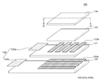
도 1은 본 발명의 일 실시예에 따른 표시 장치의 분해 사시도이다.
도 2는 본 발명의 일 실시예에 따른 표시 장치의 표시 패널의 평면도이다.
도 3은 본 발명의 일 실시예에 따른 표시 장치의 표시 패널의 분해 사시도이다.
도 4는 도 3의 IV-IV'에 따른 단면도이다.
도 5는 본 발명의 다른 실시예에 따른 표시 장치의 표시 패널의 단면도이다.
도 6은 본 발명의 또 다른 실시예에 따른 표시 장치의 표시 패널의 단면도이다.
도 7a 및 도 7b는 본 발명의 또 다른 실시예에 따른 표시 장치의 표시 패널의 단면도이다.1 is an exploded perspective view of a display device according to an exemplary embodiment.
2 is a plan view of a display panel of a display device according to an exemplary embodiment.
3 is an exploded perspective view of a display panel of a display device according to an exemplary embodiment.
4 is a cross-sectional view taken along line IV-IV' of FIG. 3 .
5 is a cross-sectional view of a display panel of a display device according to another exemplary embodiment.
6 is a cross-sectional view of a display panel of a display device according to another exemplary embodiment.
7A and 7B are cross-sectional views of a display panel of a display device according to another exemplary embodiment of the present invention.
본 발명의 이점 및 특징, 그리고, 그것들을 달성하는 방법은 첨부되는 도면과 함께 상세하게 후술되어 있는 실시예들을 참조하면 명확해질 것이다. 그러나, 본 발명은 이하에서 개시되는 실시예들에 제한되는 것이 아니라 서로 다른 다양한 형상으로 구현될 것이며, 단지 본 실시예들은 본 발명의 개시가 완전하도록 하며, 본 발명이 속하는 기술 분야에서 통상의 지식을 가진 자에게 발명의 범주를 완전하게 알려주기 위해 제공되는 것이며, 본 발명은 청구항의 범주에 의해 정의될 뿐이다.Advantages and features of the present invention, and a method of achieving them, will become apparent with reference to the embodiments described below in detail in conjunction with the accompanying drawings. However, the present invention is not limited to the embodiments disclosed below, but will be implemented in a variety of different shapes, only these embodiments allow the disclosure of the present invention to be complete, and common knowledge in the technical field to which the present invention pertains It is provided to fully inform those who have the scope of the invention, and the present invention is only defined by the scope of the claims.
본 발명의 실시예를 설명하기 위한 도면에 개시된 형상, 면적, 비율, 각도, 개수 등은 예시적인 것이므로 본 발명이 도시된 사항에 제한되는 것은 아니다. 명세서 전체에 걸쳐 동일 참조 부호는 동일 구성 요소를 지칭한다. 또한, 본 발명을 설명함에 있어서, 관련된 공지 기술에 대한 구체적인 설명이 본 발명의 요지를 불필요하게 흐릴 수 있다고 판단되는 경우 그 상세한 설명은 생략한다. 본 발명 상에서 언급된 '포함한다', '갖는다', '이루어진다' 등이 사용되는 경우 '~만'이 사용되지 않는 이상 다른 부분이 추가될 수 있다. 구성 요소를 단수로 표현한 경우에 특별히 명시적인 기재 사항이 없는 한 복수를 포함하는 경우를 포함한다.The shapes, areas, ratios, angles, numbers, etc. disclosed in the drawings for explaining the embodiments of the present invention are illustrative and the present invention is not limited to the illustrated matters. Like reference numerals refer to like elements throughout. In addition, in describing the present invention, if it is determined that a detailed description of a related known technology may unnecessarily obscure the subject matter of the present invention, the detailed description thereof will be omitted. When 'include', 'have', 'consists of', etc. mentioned in the present invention are used, other parts may be added unless 'only' is used. When a component is expressed in the singular, the case in which the plural is included is included unless otherwise explicitly stated.
구성 요소를 해석함에 있어서, 별도의 명시적 기재가 없더라도 오차 범위를 포함하는 것으로 해석한다. In interpreting the components, it is interpreted as including an error range even if there is no separate explicit description.
위치 관계에 대한 설명일 경우, 예를 들어, '~상에', '~상부에', '~하부에', '~옆에' 등으로 두 부분의 위치 관계가 설명되는 경우, '바로' 또는 '직접'이 사용되지 않는 이상 두 부분 사이에 하나 이상의 다른 부분이 위치할 수도 있다.In the case of a description of the positional relationship, for example, when the positional relationship of two parts is described as 'on', 'on', 'on', 'beside', etc., 'right' Alternatively, one or more other parts may be positioned between the two parts unless 'directly' is used.
소자 또는 층이 다른 소자 또는 층 "위 (on)"로 지칭되는 것은 다른 소자 바로 위에 또는 중간에 다른 층 또는 다른 소자를 개재한 경우를 모두 포함한다.Reference to a device or layer “on” another device or layer includes any intervening layer or other device directly on or in the middle of another device.
또한 제 1, 제 2 등이 다양한 구성 요소들을 서술하기 위해서 사용되나, 이들 구성 요소들은 이들 용어에 의해 제한되지 않는다. 이들 용어들은 단지 하나의 구성 요소를 다른 구성 요소와 구별하기 위하여 사용하는 것이다. 따라서, 이하에서 언급되는 제 1 구성 요소는 본 발명의 기술적 사상 내에서 제 2 구성 요소일 수도 있다.Also, although the first, second, etc. are used to describe various components, these components are not limited by these terms. These terms are only used to distinguish one component from another. Accordingly, the first component mentioned below may be the second component within the spirit of the present invention.
명세서 전체에 걸쳐 동일 참조 부호는 동일 구성 요소를 지칭한다.Like reference numerals refer to like elements throughout.
도면에서 나타난 각 구성의 면적 및 두께는 설명의 편의를 위해 도시된 것이며, 본 발명이 도시된 구성의 면적 및 두께에 반드시 한정되는 것은 아니다.The area and thickness of each component shown in the drawings are shown for convenience of description, and the present invention is not necessarily limited to the area and thickness of the illustrated component.
본 발명의 여러 실시예들의 각각 특징들이 부분적으로 또는 전체적으로 서로 결합 또는 조합 가능하고, 기술적으로 다양한 연동 및 구동이 가능하며, 각 실시예들이 서로에 대하여 독립적으로 실시 가능할 수도 있고 연관 관계로 함께 실시할 수도 있다.Each feature of the various embodiments of the present invention may be partially or wholly combined or combined with each other, technically various interlocking and driving are possible, and each of the embodiments may be implemented independently of each other or may be implemented together in a related relationship. may be
이하에서는 첨부된 도면을 참조하여 본 발명의 다양한 실시예들을 상세히 설명한다.Hereinafter, various embodiments of the present invention will be described in detail with reference to the accompanying drawings.
도 1은 본 발명의 일 실시예에 따른 표시 장치의 평면도이다. 도 2는 본 발명의 일 실시예에 따른 표시 장치의 표시 패널의 평면도이다. 도 2에서는 설명의 편의를 위해 표시 장치(100)의 다양한 구성 요소 중 표시 패널(120)만을 도시하였다.1 is a plan view of a display device according to an exemplary embodiment. 2 is a plan view of a display panel of a display device according to an exemplary embodiment. In FIG. 2 , only the
도 1을 참조하면, 표시 장치(100)는 백플레이트(110), 표시 패널(120), 편광판(130) 및 커버 윈도우(140)를 포함한다.Referring to FIG. 1 , the
도 1을 참조하면, 표시 패널(120)은 영상이 구현되는 패널로, 영상을 구현하기 위한 발광 소자와 발광 소자를 구동하기 위한 회로, 배선 및 부품 등이 배치될 수 있다. 표시 패널(120)은 플렉서블한 표시 패널일 수 있다. 예를 들어, 표시 패널(120)은 폴딩이 가능한 폴더블 표시 패널 또는 롤러에 와인딩이 가능한 롤러블 표시 패널일 수 있다. 이하에서는 설명의 편의를 위해 표시 패널(120)이 폴더블 표시 패널인 것으로 가정하여 설명하기로 하나, 이에 제한되지 않는다.Referring to FIG. 1 , a
표시 패널(120)은 표시 영역(AA) 및 비표시 영역(NA)을 포함한다. 그리고 표시 패널(120)은 폴딩 영역(FA) 및 비폴딩 영역(NFA)을 포함한다. 표시 패널(120)은 영상의 표시 유무에 따라 영역을 구분할 수 있으며, 폴딩 여부에 따라 영역을 구분할 수 있다. 표시 패널(120)의 특정 영역은 영상의 표시 여부 및 폴딩 여부에 따라 정의될 수 있다. 예를 들어, 표시 패널(120)의 특정 영역은 표시 영역(AA)인 동시에 폴딩 영역(FA)일 수 있다.The
표시 영역(AA)은 영상을 표시하는 영역으로, 영상을 표시하기 위한 발광 소자와 발광 소자를 구동하기 위한 회로부를 포함하는 복수의 서브 화소가 배치될 수 있다. 회로부는 유기 발광 소자를 구동하기 위한 다양한 박막 트랜지스터, 스토리지 커패시터 및 배선 등을 포함할 수 있다. 예를 들어, 회로부는 구동 박막 트랜지스터, 스위칭 박막 트랜지스터, 스토리지 커패시터, 게이트 배선 및 데이터 배선 등과 같은 다양한 구성요소를 포함할 수 있으나, 이에 제한되는 것은 아니다.The display area AA is an area for displaying an image, and a plurality of sub-pixels including a light emitting device for displaying an image and a circuit unit for driving the light emitting device may be disposed. The circuit unit may include various thin film transistors, storage capacitors, and wires for driving the organic light emitting diode. For example, the circuit unit may include various components such as a driving thin film transistor, a switching thin film transistor, a storage capacitor, a gate line, and a data line, but is not limited thereto.
비표시 영역(NA)은 영상이 표시되지 않는 영역으로, 표시 영역(AA)의 발광 소자를 구동하기 위한 회로, 배선 및 부품 등이 배치되는 영역이다. 비표시 영역(NA)에는 게이트 드라이버 IC, 데이터 드라이버 IC와 같은 구동 IC 등이 배치될 수 있다.The non-display area NA is an area in which an image is not displayed, and is an area in which circuits, wires, and components for driving the light emitting device of the display area AA are disposed. A driving IC such as a gate driver IC and a data driver IC may be disposed in the non-display area NA.
비표시 영역(NA)은 도 2에 도시된 바와 같이 표시 영역(AA)을 둘러싸는 영역으로 정의될 수 있다. 다만, 비표시 영역(NA)은 표시 영역(AA)으로부터 연장되는 영역으로 정의될 수도 있고, 또는 발광 소자가 배치되지 않는 영역으로 정의될 수도 있으며, 이에 제한되는 것은 아니다.The non-display area NA may be defined as an area surrounding the display area AA as shown in FIG. 2 . However, the non-display area NA may be defined as an area extending from the display area AA or may be defined as an area in which a light emitting device is not disposed, but is not limited thereto.
한편, 표시 패널(120)은 표시 영역(AA) 및 비표시 영역(NA)으로 정의될 수도 있으나, 폴딩 영역(FA) 및 비폴딩 영역(NFA)으로도 정의될 수 있다.Meanwhile, the
폴딩 영역(FA)은 표시 패널(120)이 폴딩되는 영역, 즉, 구부러질 수 있는 영역이다. 폴딩 영역(FA)은 폴딩 축(FX)을 기준으로 폴딩되는 영역으로, 폴딩 영역(FA)은 특정 곡률 반경으로 폴딩될 수 있다. 폴딩 영역(FA)은 표시 패널(120)이 폴딩되는 영역이므로, 폴딩 영역(FA)으로도 정의될 수 있다. 폴딩 영역(FA)은 폴딩 축(FX)에 인접한 표시 영역(AA)의 일부 및 비표시 영역(NA)의 일부를 포함한다.The folding area FA is an area in which the
도 2에서는 폴딩 축(FX)이 표시 패널(120)의 중앙에 배치된 것으로 도시하였으나, 폴딩 축(FX)의 위치 및 개수는 다양하게 변경될 수 있고, 폴딩 축(FX)의 위치 및 개수에 따라 폴딩 영역(FA) 또한 다양하게 변경될 수 있으며, 이에 제한되는 것은 아니다.Although FIG. 2 illustrates that the folding axis FX is disposed in the center of the
비폴딩 영역(NFA)은 표시 패널(120)이 평평한 상태를 유지하는 영역이다. 비폴딩 영역(NFA)은 표시 영역(AA)의 일부 및 비표시 영역(NA)의 일부를 포함한다. 비폴딩 영역(NFA)은 표시 패널(120)이 폴딩되지 않는 영역으로, 비폴딩 영역(NFA)으로도 정의될 수 있다. 비폴딩 영역(NFA)은 폴딩 영역(FA)의 양측으로 연장될 수 있다. 폴딩 영역(FA)을 사이에 두고 2개의 비폴딩 영역(NFA)이 배치될 수 있다.The non-folding area NFA is an area in which the
비폴딩 영역(NFA)은 제1 비폴딩 영역(NFA1) 및 제2 비폴딩 영역(NFA2)을 포함한다. 제1 비폴딩 영역(NFA1)은 폴딩 축(FX)의 좌측으로 연장된 비폴딩 영역(NFA)이다. 제2 비폴딩 영역(NFA2)은 폴딩 축(FX)의 우측으로 연장된 비폴딩 영역(NFA)이다. The non-folding area NFA includes a first non-folding area NFA1 and a second non-folding area NFA2 . The first non-folding area NFA1 is a non-folding area NFA extending to the left of the folding axis FX. The second non-folding area NFA2 is a non-folding area NFA extending to the right of the folding axis FX.
표시 장치(100)가 펼쳐진 비폴딩 상태일 때, 폴딩 영역(FA)과 비폴딩 영역(NFA)은 일 평면을 이룰 수 있다. 예를 들어, 표시 장치(100)가 평탄하게 펼쳐진 비폴딩 상태일 때, 폴딩 영역(FA)과 제1 비폴딩 영역(NFA1) 및 제2 비폴딩 영역(NFA2)은 일 평면을 이룰 수 있다. When the
표시 장치(100)가 폴딩된 폴딩 상태일 때, 폴딩 영역(FA) 양측의 비폴딩 영역(NFA)은 평탄한 상태를 유지하며 서로 마주보도록 배치될 수 있다. 이때, 표시 장치(100)는 표시 장치(100)의 폴딩 방향에 따라 표시 장치(100)의 상면 또는 하면에서 제1 비폴딩 영역(NFA1)과 제2 비폴딩 영역(NFA2)이 서로 마주보도록 배치될 수 있다. 예를 들어, 표시 장치(100)가 인 폴딩되는 경우, 표시 장치(100)는 제1 비폴딩 영역(NFA1) 및 제2 비폴딩 영역(NFA2)에 각각 중첩하는 표시 장치(100)의 상면이 서로 마주하도록 폴딩될 수 있다. 반대로 표시 장치(100)가 아웃 폴딩되는 경우, 표시 장치(100)는 제1 비폴딩 영역(NFA1) 및 제2 비폴딩 영역(NFA2)에 각각 중첩하는 표시 장치(100)의 하면이 서로 마주하도록 폴딩될 수 있다. 이하에서는 설명의 편의를 위해, 본 발명의 일 실시예에 따른 표시 장치(100)는 인 폴딩 되는 것으로 가정하여 설명하기로 하나, 이에 제한되지 않는다.When the
다시, 도 1을 참조하면, 커버 윈도우(140)는 커버 윈도우(140) 하부의 편광판(130), 표시 패널(120) 등을 외부의 충격, 습기, 열 등으로부터 보호할 수 있다. 커버 윈도우(140)는 내충격성 및 광투과성을 갖는 물질로 이루어질 수 있다. 예를 들어, 커버 윈도우(140)는 유리로 이루어진 기판이거나, 폴리메틸메타아크릴레이트(polymethylmethacrylate, PMMA), 폴리이미드(Polyimide, PI), 폴리에틸렌 테레프탈레이트(polyethylene terephthalate, PET)와 같은 플라스틱 물질로 이루어진 박형의 필름일 수 있으나, 이에 제한되지 않는다.Again, referring to FIG. 1 , the
커버 윈도우(140)는 외부의 충격으로 인한 크랙을 저감하기 위해, 인장영률이자 모듈러스 값이 큰 재질, 즉 고경도의 재질로 구성될 수 있다. 모듈러스 값이 큰 재질의 경우, 표시 장치(100)가 폴딩될 때 휘어지지 않고 깨질 수 있다. 그러나, 모듈러스 값이 큰 재질이라도 일정 두께 이하가 되면 폴딩이 가능할 수 있다. 따라서, 커버 윈도우(140)는 매우 얇은 두께를 가질 수 있다. 예를 들어, 커버 윈도우(140)는 박형의 플라스틱 필름일 수 있으며, 이에 제한되지 않는다.The
한편, 도면에 도시되지는 않았으나, 커버 윈도우(140)의 표면 경도를 향상시키기 위해, 커버 윈도우(140)의 일면 또는 양면에 하드 코팅층이 더 배치될 수 있으며, 이에 제한되지 않는다.Meanwhile, although not shown in the drawings, a hard coating layer may be further disposed on one or both surfaces of the
커버 윈도우(140) 하부에 편광판(130)이 배치된다. 편광판(130)은 선택적으로 광을 투과시켜 표시 패널(120)로 입사하는 외부 광의 반사를 저감할 수 있다. 구체적으로, 표시 패널(120)은 박막 트랜지스터, 배선, 발광 소자 등에 적용되는 다양한 금속 물질을 포함한다. 이에, 표시 패널(120)로 입사된 외광은 금속 물질로부터 반사될 수 있고, 외광의 반사로 인해 표시 장치(100)의 시인성이 저감될 수 있다. 따라서, 표시 패널(120)의 일면에 편광판(130)을 배치하여 외광의 반사를 방지할 수 있고, 표시 장치(100)의 야외 시인성을 높일 수 있다. 다만, 도 1 및 도 2의 표시 장치(100)의 구성 요소는 예시적인 것이며, 편광판(130)은 표시 장치(100)의 구현예에 따라 생략될 수도 있다.A
한편, 표시 패널(120)과 편광판(130) 사이에 터치 패널이 더 배치될 수 있다. 터치 패널은 폴더블 표시 장치(100)에 대한 화면 터치나 제스쳐 등과 같은 사용자의 터치 입력을 감지하는 구성으로, 정전용량 방식, 등으로 구현될 수 있다.Meanwhile, a touch panel may be further disposed between the
표시 패널(120) 하부에 백플레이트(110)가 배치된다. 표시 패널(120)을 이루는 기판이 폴리이미드와 같은 플라스틱 물질로 이루어지는 경우, 기판 하부에 유리로 이루어지는 지지 기판을 부착한 후 표시 장치(100)의 제조 공정이 진행되고, 표시 패널(120) 상에 편광판(130) 등의 구성 요소를 형성한 후 지지 기판이 탈착될 수 있다. 그리고 지지 기판이 탈착된 후, 기판을 지지하기 위한 백플레이트(110)가 표시 패널(120)의 기판 하부에 배치될 수 있다. 백플레이트(110)는 표시 패널(120)을 지지할 뿐만 아니라, 표시 패널(120)을 외부의 습기, 열, 충격 등으로부터 보호할 수 있다.The
한편, 표시 장치(100)의 각 구성 요소 사이에는 접착층이 배치될 수 있다. 접착층은 표시 장치(100)의 다른 구성 요소들 사이에 배치되어, 각각의 구성 요소를 다른 구성 요소와 접착시킨다. 구체적으로, 접착층은 커버 윈도우(140)와 편광판(130) 사이, 편광판(130)과 표시 패널(120) 사이, 표시 패널(120)과 백플레이트(110) 사이에 각각 배치될 수 있다. 접착층은 접착성을 갖는 물질로 이루어질 수 있고, 예를 들어, OCA(Optical Clear Adhesive), PSA(Pressure Sensitive Adhesive) 등으로 이루어질 수 있으나, 이에 제한되지 않는다.Meanwhile, an adhesive layer may be disposed between each component of the
한편, 도면에 도시되지는 않았으나, 백플레이트(110) 하부에 미드 프레임이 더 배치될 수 있다. 미드 프레임은 금속 등의 강성 재료로 이루어져 미드 프레임 상의 백플레이트(110), 표시 패널(120) 등을 보호 및 지지할 수 있다. Meanwhile, although not shown in the drawings, a mid frame may be further disposed under the
이하에서는 표시 패널(120)에 대한 보다 상세한 설명을 위해 도 3 및 도 4를 함께 참조한다.Hereinafter, referring to FIGS. 3 and 4 together for a more detailed description of the
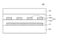
도 3은 본 발명의 일 실시예에 따른 표시 장치의 표시 패널의 분해 사시도이다. 도 4는 도 3의 IV-IV'에 따른 단면도이다. 도 3에서는 설명의 편의를 위하여, 디지타이저(122)의 제1 전극(122a) 및 제2 전극(122b)과 인쇄 회로 기판(126)을 연결하는 배선의 도시를 생략하였다.3 is an exploded perspective view of a display panel of a display device according to an exemplary embodiment. 4 is a cross-sectional view taken along line IV-IV' of FIG. 3 . In FIG. 3 , a wiring connecting the
도 3 및 도 4를 참조하면, 표시 패널(120)은 절연 부재(125), 제1 기판(121), 디지타이저(122), 무기 절연층(123), 제2 기판(124) 및 발광 소자를 포함한다.3 and 4 , the
절연 부재(125)는 표시 패널(120)의 최하단에 배치된다. 절연 부재(125)는 유기 절연층 또는 무기 절연층으로 이루어져, 절연 부재(125) 상에 배치되는 구성 요소들을 보호할 수 있다. 예를 들어, 절연 부재(125)가 유기 절연층으로 이루어지는 경우, 아크릴계 수지, 에폭시 수지, 페놀 수지, 폴리아미드계 수지, 폴리이미드계 수지, 불포화 폴리에스테르계 수지, 폴리페닐렌계 수지, 폴리페닐렌설파이드계 수지, 벤조사이클로부텐 및 포토레지스트 중 하나로 형성될 수 있으나, 이에 제한되는 것은 아니다. 또한, 절연 부재(125)가 무기 절연층으로 이루어지고, 수분이나 산소의 침투를 억제할 수 있다. 절연 부재(125)는 실리콘 질화물(SiNx), 실리콘 산질화물(SiNxOy) 또는 산화알루미늄(AlyOz) 등으로 이루어질 수 있으나, 이에 제한되는 것은 아니다.The insulating
절연 부재(125) 상에는 디지타이저(122)가 배치된다. 디지타이저(122)는 펜(pen) 또는 사용자의 터치 입력에 따른 X, Y 좌표를 디지털 형식으로 변환하여 사용자의 터치 입력에 대응하여 표시 패널(120)에 시각적으로 구현해낼 수 있다. 디지타이저(122)는, 예를 들어, 압력 센서일 수 있으나, 이에 제한되는 것은 아니다.A
디지타이저(122)는 제1 전극(122a) 및 제2 전극(122b)을 포함한다. 제1 전극(122a) 및 제2 전극(122b)은 투명 전도성 물질 또는 금속 물질로 이루어질 수 있다. 예를 들어, 제1 전극(122a) 및 제2 전극(122b)이 투명 전도성 물질로 이루어지는 경우, 인듐 주석 산화물(ITO; Indium Tin Oxide), 인듐 아연 산화물(IZO; Indium Zinc Oxide), 인듐 주석 아연 산화물(ITZO; Indium Tin Zinc Oxide)로 이루어질 수 있고, 제1 전극(122a) 및 제2 전극(122b)이 금속 물질로 이루어지는 경우, 몰리브덴(Mo), 알루미늄(Al), 크롬(Cr), 금(Au), 티타늄(Ti), 니켈(Ni), 네오디뮴(Nd), 및 구리(Cu) 중 어느 하나이거나 둘 이상의 합금, 또는 이들의 다중층으로 이루어질 수 있다. 또한, 제1 전극(122a) 및 제2 전극(122b)은 나노 와이어(AgNW), 탄소 나노 튜브(CNT), 그라핀(Graphene) 등의 유연 물질로 이루어질 수도 있다. 다만, 제1 전극(122a) 및 제2 전극(122b)은 서로 동일한 물질로 이루어질 수 있으나, 이에 제한되는 것은 아니고, 제1 전극(122a) 및 제2 전극(122b)은 서로 상이한 물질로 이루어질 수도 있다.The
제1 전극(122a)은 절연 부재(125) 상에 배치될 수 있다. 제1 전극(122a)은, 예를 들어, 막대 형상으로 형성되어, X축 방향인 제1 방향으로 배치될 수 있다. 이때, 제1 방향은 절연 부재(125)의 길이 방향과 동일한 방향일 수 있다. 도 3에서는 제1 전극(122a)이 4개인 것으로 도시하였으나, 제1 전극(122a)의 개수는 설계에 따라 다양하게 변경될 수 있으며, 이에 제한되지 않는다.The
제1 전극(122a) 상에 제1 기판(121)이 배치된다. 제1 기판(121)은 제1 전극(122a)을 덮도록 배치되어, 제1 기판(121) 상에 배치되는 여러 구성요소들을 지지하고 보호할 수 있다. 제1 기판(121)은 유리전이온도(transition temperature; TG)가 높은 절연 물질로 이루어질 수 있다. 예를 들어, 제1 기판(121)은 유색 폴리이미드(polyimide), 폴리에틸렌 나프탈레이트(polyethylene naphthalate; PEN), 아라마이드(aramide) 등과 같은 내열성이 높고, 플렉서빌리티(flexability)를 가지는 플라스틱(plastic) 물질로 이루어질 수 있다. A
제1 기판(121) 상에 제2 전극(122b)이 배치된다. 제2 전극(122b)은, 예를 들어, 막대 형상으로 형성되어, 제1 전극(122a)과 중첩하게 배치될 수 있다. 또한, 제2 전극(122b)은 제1 전극(122a)이 배치되는 제1 방향과 상이한 제2 방향으로 배치될 수 있다. 제1 방향과 제2 방향은 서로 수직한 방향일 수 있으나, 이에 제한되는 것은 아니다. 도 3에서는 제2 전극(122b)이 4개인 것으로 도시하였으나, 제2 전극(122b)의 개수는 설계에 따라 다양하게 변경될 수 있으며, 이에 제한되지 않는다.A
디지타이저(122)의 제1 전극(122a)과 제2 전극(122b)은 제1 기판(121)을 사이에 두고 커패시터를 구성하여, 제1 전극(122a)과 제2 전극(122b) 사이의 커패시턴스 변화량에 기초하여 터치 입력의 세기가 측정될 수 있다. 이에, 제1 전극(122a)과 제2 전극(122b) 사이에 커패시턴스가 형성되도록 제2 전극(122b)에 소정의 전압이 인가될 수 있고, 제2 전극(122b)은 접지되거나 제2 전극(122b)에 인가된 전압과 상이한 전압이 인가될 수 있다. 예를 들어, 강한 터치 입력이 인가되는 경우, 제1 기판(121)이 압축되어 제1 전극(122a) 및 제2 전극(122b) 사이의 간격이 감소될 수 있다. 이에, 제1 전극(122a) 및 제2 전극(122b) 사이에 커패시턴스의 변화가 발생한다. 반면에, 약한 터치 입력이 인가되는 경우, 제1 기판(121)은 상대적으로 약하게 압축되어, 제1 전극(122a) 및 제2 전극(122b) 사이의 간격이 상대적으로 작게 감소될 수 있다. 이에, 제1 전극(122a) 및 제2 전극(122b) 사이의 커패시턴스는 약하게 변화할 수 있다. 따라서, 제1 전극(122a) 및 제2 전극(122b) 사이의 커패시턴스를 측정함으로써, 터치 입력의 세기가 측정될 수 있다. 다만, 이에 제한되지 않고 디지타이저(122)의 측정 방식으로 다른 방식이 사용될 수도 있다.The
제1 기판(121) 및 제2 전극(122b) 상에 무기 절연층(123)이 배치된다. 무기 절연층(123)은 제2 전극(122b)을 덮도록 배치되어, 제2 전극(122b)을 외부의 수분, 산소, 충격 등으로부터 보호할 수 있다. 무기 절연층(123)은 실리콘 질화물(SiNx), 실리콘 산화질화물(SiON) 등과 같은 무기물로 이루어질 수 있으나, 이에 제한되지 않는다.An inorganic insulating
무기 절연층(123) 상에 제2 기판(124)이 배치된다. 제2 기판(124)은 무기 절연층(123)과 동일한 크기로 형성될 수 있다. 그리고, 제2 기판(124)은 제1 기판(121)과 동일한 물질로 이루어질 수 있으나, 이에 제한되는 것은 아니다.A
한편, 도 3 및 도 4에는 도시되지 않았으나, 제2 기판(124) 상에는 박막 트랜지스터 및 발광 소자가 배치될 수 있다. 발광 소자는 박막 트랜지스터로부터 전기적 신호를 전달받음으로써, 표시 장치(100)의 화소를 구성할 수 있다.Meanwhile, although not shown in FIGS. 3 and 4 , a thin film transistor and a light emitting device may be disposed on the
다시 도 3을 참조하면, 표시 장치(100)는 인쇄 회로 기판(126)을 더 포함할 수 있다. 인쇄 회로 기판(126)은 디지타이저(122)로 전기적인 신호를 전달하거나 전달받을 수 있다. 예를 들어, 인쇄 회로 기판(126)에는 IC 칩, 회로부, 메모리 등과 같은 다양한 구성이 실장될 수 있으나, 이에 제한되는 것은 아니다. Referring back to FIG. 3 , the
도 3을 참조하면, 인쇄 회로 기판(126)은 제1 인쇄 회로 기판(126a) 및 제2 인쇄 회로 기판(126b)으로 구성되어, 각각 제1 기판(121) 및 절연 부재(125)에 본딩될 수 있다. Referring to FIG. 3 , the printed
제1 기판(121)은 가장자리에 제1 인쇄 회로 기판(126a)이 본딩될 수 있도록, 제2 기판(124)보다 큰 크기로 형성될 수 있다. 즉, 제1 기판(121) 중 일부는 제2 기판(124)과 중첩하고, 다른 일부는 제2 기판(124)과 중첩하지 않을 수 있다. 이에, 제1 인쇄 회로 기판(126a)은 제1 기판(121) 중 제2 기판(124)과 중첩하지 않는 영역, 즉, 제2 기판(124)보다 돌출된 제1 기판(122)의 패드 영역에 본딩되어, 디지타이저(122)의 제2 전극(122b)과 제1 기판(122) 상에 형성된 패드 및 배선을 통해 전기적으로 연결될 수 있다. The
마찬가지로, 절연 부재(125)는 가장자리에 제2 인쇄 회로 기판(126b)이 본딩될 수 있도록, 제1 기판(121)보다 큰 크기로 형성될 수 있다. 즉, 절연 부재(125) 중 일부는 제1 기판(121)과 중첩하고, 다른 일부는 제1 기판(121)과 중첩하지 않을 수 있다. 이에, 제2 인쇄 회로 기판(126b)은 절연 부재(125) 중 제1 기판(121)과 중첩하지 않는 영역, 즉, 제1 기판(121)보다 돌출된 절연 부재(125)의 패드 영역에 본딩되어, 디지타이저(122)의 제1 전극(122a)과 절연 부재(125) 상에 형성된 패드 및 배선을 통해 전기적으로 연결될 수 있다. Similarly, the insulating
한편, 표시 패널(120)은 유리로 이루어지는 지지 기판 상에 절연 부재(125), 디지타이저(122), 제1 기판(121), 무기 절연층(123), 제2 기판(124) 및 발광 소자 등의 구성 요소가 형성된 후, 지지 기판이 탈착될 수 있다. 구체적으로, 지지 기판 상에 절연 부재(125)가 형성되고, 절연 부재(125) 상에 디지타이저(122)의 제1 전극(122a)이 증착 및 에칭되어 형성될 수 있다. 그 다음, 디지타이저(122)의 제1 전극(122a)을 덮도록 제1 기판(121)이 형성되고, 제1 기판(121) 상에 디지타이저(122)의 제2 전극(122b)이 증착 및 에칭되어 형성될 수 있다. 그리고, 제2 전극(122b)을 덮도록 무기 절연층(123)이 형성되고, 무기 절연층(123) 상에 제2 기판(124) 및 발광 소자가 형성될 수 있다. 이에, 표시 패널(120)의 모든 구성 요소들이 지지 기판 상에 형성된 후, 지지 기판이 절연 부재(125)로부터 탈착되어, 표시 패널(120)을 제조할 수 있다.Meanwhile, the
일반적인 표시 장치에서는 표시 패널의 하부에 별도의 기판 또는 필름(film)의 형태로 디지타이저를 구성하였다. 그러나, 디지타이저는 기판의 상부 및 하부에 전극을 교차하여 설계하므로, 디지타이저를 별도의 기판이나 필름 형태로 구성하는 경우, 표시 장치의 두께가 증가할 수 있다. 특히, 디지타이저를 폴더블 표시 장치, 롤러블 표시 장치 등의 플렉서블 표시 장치에 적용하는 경우, 표시 장치의 두께 증가로 인해 표시 장치에 큰 스트레스가 발생할 수 있으며, 이에, 필름 형태의 디지타이저를 플렉서블 표시 장치에 적용하는 것에 어려움이 있었다.In a general display device, a digitizer is configured in the form of a separate substrate or film under the display panel. However, since the digitizer is designed by crossing electrodes on the upper and lower portions of the substrate, the thickness of the display device may increase when the digitizer is configured in the form of a separate substrate or film. In particular, when a digitizer is applied to a flexible display device such as a foldable display device or a rollable display device, a great stress may occur in the display device due to an increase in the thickness of the display device. There were difficulties in applying it.
이에, 본 발명의 일 실시예에 따른 표시 장치(100)에서는, 제1 기판(121)에 디지타이저(122)를 구현하여, 표시 장치(100)의 전체 두께를 저감할 수 있다. 예를 들어, 디지타이저(122)의 제1 전극(122a)은 제1 기판(121)의 하면에 배치되고, 제2 전극(122b)은 제1 기판(121)의 상면에 배치될 수 있다. 이에, 표시 패널(120)에 인가되는 터치 입력의 세기에 따라 제1 기판(121)이 압축되고, 제1 전극(122a) 및 제2 전극(122b)사이의 커패시턴스 변화로 터치 입력의 세기가 측정될 수 있다. 따라서, 제1 기판(121)에 디지타이저(122)를 구현함으로써, 표시 장치(100)에 구성되는 별도의 디지타이저(122)가 생략될 수 있고, 이에, 두께가 저감된 표시 장치(100)를 구현할 수 있다.Accordingly, in the
또한, 본 발명의 일 실시예에 따른 표시 장치(100)에서는 제1 기판(121)을 유리전이온도가 높은 물질로 구성하여, 디지타이저(122) 형성 공정 시, 제1 기판(121)이 손상되는 것을 저감할 수 있다. 디지타이저(122)의 제1 전극(122a) 및 제2 전극(122b)은 금속 물질 또는 투명 전도성 물질을 제1 기판(121)에 증착 또는 에칭(etching)하여 형성될 수 있다. 즉, 디지타이저(122) 형성 공정은 고온에서 수행되어, 제1 기판(121)의 유리전이온도가 낮은 경우, 제1 기판(121)이 손상될 수 있다. 이에, 본 발명의 일 실시예에 따른 표시 장치(100)에서는 제1 기판(121)을 유리전이온도가 높고 내열성이 강한 물질로 형성하여, 디지타이저(122) 형성 공정 시, 제1 기판(121)의 손상을 저감할 수 있다.In addition, in the
도 5는 본 발명의 다른 실시예에 따른 표시 장치의 표시 패널의 단면도이다. 도 5의 표시 장치(500)는 도 1 내지 도 4의 표시 장치(100)와 비교하여 보호층(527)만이 추가되었을 뿐, 다른 구성은 실질적으로 동일하므로 중복 설명을 생략한다.5 is a cross-sectional view of a display panel of a display device according to another exemplary embodiment. Compared to the
도 5를 참조하면, 표시 장치(500)는 보호층(527)을 포함한다. 보호층(527)은 절연 부재(125)의 상면 및 제1 기판(121)의 상면과 접하도록 배치된다. 보호층(527)은 절연 부재(125) 및 제1 기판(121)에 디지타이저(122)의 제1 전극(122a) 및 제2 전극(122b)을 증착하거나 에칭하는 경우, 절연 부재(125) 제1 기판(121)이 손상되는 것을 저감할 수 있다. Referring to FIG. 5 , the
보호층(527)은 프라이머층(primer layer) 또는 무기 절연 물질로 이루어질 수 있다. 예를 들어, 보호층(527)이 프라이머층으로 이루어지는 경우, 보호층(527)은 아크릴계 점착제, 우레탄계, 아크릴 수지, 우레탄 수지 등으로 이루어진 프라이머층일 수 있으나, 이에 제한되는 것은 아니다. 또한, 보호층(527)이 무기 절연 물질로 이루어지는 경우, 무기 절연층(123)과 종일한 물질로 이루어질 수 있으나, 이에 제한되는 것은 아니다.The protective layer 527 may be formed of a primer layer or an inorganic insulating material. For example, when the protective layer 527 is made of a primer layer, the protective layer 527 may be a primer layer made of an acrylic adhesive, urethane, acrylic resin, urethane resin, or the like, but is not limited thereto. In addition, when the protective layer 527 is made of an inorganic insulating material, it may be made of the same material as the inorganic insulating
보호층(527)은 제1 보호층(527a) 및 제2 보호층(527b)을 포함한다. The passivation layer 527 includes a
제1 보호층(527a)은 제1 기판(121)과 제1 전극(122a) 하부에서 절연 부재(125)의 상면과 접하도록 배치될 수 있다. 즉, 제1 보호층(527a)은 절연 부재(125) 및 제1 기판(121)과 제1 전극(122a) 사이에 배치될 수 있다. 제1 보호층(527a)은 절연 부재(125)의 상면 상에 배치되어, 제1 기판(121) 및 제1 전극(122a)의 하면과 접하도록 배치될 수 있다. The
제2 보호층(527b)은 제1 기판(121)의 상면과 접하도록 배치된다. 그리고, 제2 보호층(527b) 상에는 제2 전극(122b)이 배치될 수 있다. 이에, 제2 보호층(527b)은 제2 전극(122b)과 무기 절연층(123) 및 제1 기판(121) 사이에 배치될 수 있다.The
한편, 디지타이저(122)의 제1 전극(122a) 및 제2 전극(122b)은 보호층(527)이 형성된 후에 형성될 수 있다. 구체적으로, 제1 보호층(527a)이 절연 부재(125) 상에 형성되고, 제1 보호층(527a) 상에 제1 전극(122a)이 증착 및 에칭되어 형성될 수 있다. 그리고, 디지타이저(122)의 제1 전극(122a)을 덮도록 제1 기판(121)이 형성되고, 제1 기판(121) 상에 제2 보호층(527b)이 형성된 후, 제2 보호층(527b) 상에 제2 전극(122b)이 증착 및 에칭되어 형성될 수 있다. 그리고, 제2 전극(122b)을 덮도록 무기 절연층(123)이 형성되고, 무기 절연층(123) 상에 제2 기판(124) 및 발광 소자가 형성될 수 있다.Meanwhile, the
본 발명의 다른 실시예에 따른 표시 장치(500)에서는 절연 부재(125)의 상면 및 제1 기판(121)의 상면에 보호층(527)을 배치하여 디지타이저(122) 형성 공정 시, 절연 부재(125) 및 제1 기판(121)이 손상되는 것을 저감할 수 있다. 디지타이저(122)의 제1 전극(122a) 및 제2 전극(122b)은 절연 부재(125) 및 제1 기판(121)에 증착하거나 에칭하여 형성될 수 있다. 구체적으로, 제1 전극(122a)은 절연 부재(125) 상에 형성되고, 제2 전극(122b)은 제1 기판(121) 상에 형성될 수 있다. 이때, 절연 부재(125) 및 제1 기판(121)은 고온으로 인해 변형되거나, 일부가 식각되어 손상될 수 있다. 따라서, 절연 부재(125)의 상면 및 제1 기판(121)의 상면에 보호층(527)을 배치하여, 증착 또는 에칭 공정이 수행되더라도, 절연 부재(125) 및 제1 기판(121)이 손상되는 것을 저감할 수 있다. In the
도 6은 본 발명의 다른 실시예에 따른 표시 장치의 표시 패널의 단면도이다. 도 6의 표시 장치(600)는 도 1 내지 도 4의 표시 장치(100)와 비교하여 절연 부재(625)만이 상이할 뿐, 다른 구성은 실질적으로 동일하므로 중복 설명을 생략한다.6 is a cross-sectional view of a display panel of a display device according to another exemplary embodiment. Compared to the
도 6을 참조하면, 제1 기판(121) 및 제1 전극(122a)의 하부에 절연 부재(625)가 배치된다. 절연 부재(625)는 제1 기판(121) 또는 제2 기판(124)과 동일한 물질로 이루어지는 제3 기판(625)일 수 있다. 즉, 제3 기판(625)은 유색 폴리이미드(polyimide), 폴리에틸렌 나프탈레이트(polyethylene naphthalate; PEN), 아라마이드(aramide) 등과 같은 내열성이 높고, 플렉서빌리티(flexability)를 가지는 플라스틱(plastic) 물질로 이루어져, 제1 기판(121)의 하면 및 제1 전극(122a)의 하면과 접하도록 배치될 수 있다. 이에, 제1 전극(122a)은 제3 기판(625)에 의해 절연될 수 있다.Referring to FIG. 6 , an insulating
한편, 표시 장치(600)의 표시 패널은 유리로 이루어지는 지지 기판 상에 제3 기판(625), 디지타이저(122), 제1 기판(121), 무기 절연층(123), 제2 기판(124) 및 발광 소자 등의 구성 요소가 형성된 후, 지지 기판이 탈착될 수 있다. 구체적으로, 지지 기판 상에 제3 기판(625)이 형성되고, 제3 기판(625) 상에 디지타이저(122)의 제1 전극(122a)이 증착 및 에칭되어 형성될 수 있다. 그 다음, 디지타이저(122)의 제1 전극(122a)을 덮도록 제1 기판(121)이 형성되고, 제1 기판(121) 상에 디지타이저(122)의 제2 전극(122b)이 증착 및 에칭되어 형성될 수 있다. 그리고, 제2 전극(122b)을 덮도록 무기 절연층(123)이 형성되고, 무기 절연층(123) 상에 제2 기판(124) 및 발광 소자가 형성될 수 있다. 이에, 도 6의 표시 장치(600)의 표시 패널의 모든 구성 요소들이 지지 기판 상에 형성된 후, 지지 기판이 제3 기판(625)으로부터 탈착되어, 표시 패널을 제조할 수 있다.Meanwhile, the display panel of the
본 발명의 또 다른 실시예에 따른 표시 장치(600)에서는 제1 기판(121) 및 제1 전극(122a)의 하부에 제3 기판(625)을 배치하여, 제3 기판(625) 상에 배치되는 구성 요소들을 보호할 수 있다. 제3 기판(625)은 제1 기판(121) 또는 제2 기판(124)과 동일한 물질로 이루어져, 제1 기판(121)의 하면 및 제1 전극(122a)의 하면을 덮도록 배치될 수 있다. 예를 들어, 제3 기판(625)은 폴리이미드, 폴리에틸렌나프탈레이트, 아라마이드 등과 같은 유리전이온도가 높고, 내열성이 좋은 물질로 이루어질 수 있다. 이에, 제3 기판(625)은 제1 전극(122a)을 외부의 수분 및 산소로부터 보호함과 동시에, 제1 기판(121) 및 제2 기판(124) 상에 배치되는 박막 트랜지스터 및 발광 소자를 충격으로부터 보호할 수 있다.In the
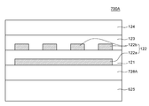
도 7a 및 도 7b는 본 발명의 또 다른 실시예에 따른 표시 장치의 표시 패널의 단면도이다. 도 7a 및 도 7b의 표시 장치(700A, 700B)는 도 6의 표시 장치(600)와 비교하여 무기 절연층(728A, 728B)만이 추가되었을 뿐, 다른 구성은 실질적으로 동일하므로 중복 설명을 생략한다.7A and 7B are cross-sectional views of a display panel of a display device according to another exemplary embodiment of the present invention. Compared to the
도 7a 및 도 7b를 참조하면, 표시 장치(700A, 700B)는 제1 기판(121) 및 제3 기판(625) 사이에 무기 절연층(728A, 728B)을 더 포함할 수 있다. 무기 절연층(728A, 728B)은 제3 기판(625) 상에 배치되어, 제3 기판(625) 상에 배치되는 구성 요소들을 외부의 수분, 산소, 충격 등으로부터 보호할 수 있다. 무기 절연층(728A, 728B)은 제2 전극(122b) 상에 배치되는 무기 절연층(728A, 728B)과 동일한 물질일 수 있으나, 이에 제한되는 것은 아니다.7A and 7B , the
도 7a를 참조하면, 무기 절연층(728A)은 제1 기판(121)의 하면 및 제1 전극(122a)의 하면과 접하도록 배치될 수 있다. 이에, 무기 절연층(728A)의 상면은 제1 기판(121)의 하면 및 제1 전극(122a)의 하면과 접하고, 하면은 제3 기판(625)의 상면과 접하도록 배치될 수 있다.Referring to FIG. 7A , the inorganic insulating
한편, 도 7a에서 디지타이저(122)의 제1 전극(122a)은 무기 절연층(728A)이 형성된 후에 형성될 수 있다. 구체적으로, 제3 기판(625) 상에 무기 절연층(728A)이 형성되고, 무기 절연층(728A) 상에 제1 전극(122a)이 증착 및 에칭되어 형성될 수 있다. 그리고, 디지타이저(122)의 제1 전극(122a)을 덮도록 제1 기판(121)이 형성되고, 제1 기판(121) 상에 제2 전극(122b)이 증착 및 에칭되어 형성될 수 있다. 그리고, 제2 전극(122b)을 덮도록 무기 절연층(123)이 형성되고, 무기 절연층(123) 상에 제2 기판(124) 및 발광 소자가 형성될 수 있다.Meanwhile, in FIG. 7A , the
또한, 도 7b를 참조하면, 무기 절연층(728B)은 제3 기판(625) 상에 배치되는 제1 전극(122a)을 덮도록 배치될 수 있다. 이에, 무기 절연층(728B)은 제3 기판(625)의 상면 및 제1 기판(121)의 상면 및 측면을 덮도록 배치되고, 무기 절연층(728B)의 상면은 제1 기판(121)의 하면과 접하도록 배치될 수 있다.Also, referring to FIG. 7B , the inorganic insulating
한편, 도 7b에서 디지타이저(122)의 제1 전극(122a)은 제3 기판(625) 상에서 증착 및 에칭되어 형성될 수 있다. 그리고, 디지타이저(122)의 제1 전극(122a)을 덮도록 무기 절연층(728B)이 형성되고, 무기 절연층(728B) 상에 제1 기판(121)이 형성될 수 있다. 그리고, 제1 기판(121) 상에 제2 전극(122b)이 증착 및 에칭되어 형성될 수 있고, 제2 전극(122b)을 덮도록 무기 절연층(123)이 형성된 후, 무기 절연층(123) 상에 제2 기판(124) 및 발광 소자가 형성될 수 있다. Meanwhile, in FIG. 7B , the
본 발명의 또 다른 실시예에 따른 표시 장치(700A, 700B)에서는 제1 기판(121) 및 제3 기판(625) 사이에 무기 절연층(728A, 728B)을 배치하여, 제1 전극(122a)을 외부의 수분 및 산소로부터 보호할 수 있다. 제1 전극(122a)은 전도성 물질로 이루어져, 수분 및 산소에 취약할 수 있다. 이에, 무기 절연층(728A, 728B)이 제1 기판(121)과 제3 기판(625) 사이에서 제1 전극(122a)의 하면을 덮도록 배치되거나, 제1 전극(122a)을 감싸도록 배치되어, 외부의 수분 및 산소로부터 제1 전극(122a)을 보호할 수 있다.In the
본 발명의 실시예들에 따른 표시 장치는 다음과 같이 설명될 수 있다.Display devices according to embodiments of the present invention may be described as follows.
본 발명의 일 실시예에 따른 표시 장치는, 플렉서빌리티(flexibility)를 갖는 제1 기판, 제1 기판의 하부에서 제1 방향으로 배치되는 제1 전극 및 제1 기판 상에서 제1 방향과 상이한 제2 방향으로 배치되는 제2 전극을 포함하는 디지타이저, 제1 기판 상에서 제2 전극을 덮도록 배치되는 무기 절연층, 무기 절연층 상에 배치되는 제2 기판, 및 제2 기판 상에 배치되는 발광 소자를 포함할 수 있다.A display device according to an embodiment of the present invention includes a first substrate having flexibility, a first electrode disposed under the first substrate in a first direction, and a first electrode different from the first direction on the first substrate. A digitizer including a second electrode disposed in two directions, an inorganic insulating layer disposed on a first substrate to cover the second electrode, a second substrate disposed on the inorganic insulating layer, and a light emitting device disposed on the second substrate may include.
본 발명의 다른 특징에 따르면, 표시 장치는 제1 기판과 제1 전극 하부에 배치되는 제1 보호층, 및 제1 기판과 제2 전극 사이에 배치되는 제2 보호층을 더 포함할 수 있다.According to another feature of the present invention, the display device may further include a first passivation layer disposed under the first substrate and the first electrode, and a second passivation layer disposed between the first substrate and the second electrode.
본 발명의 또 다른 특징에 따르면, 제1 보호층 및 제2 보호층은 프라이머층 또는 무기 절연 물질로 이루어질 수 있다.According to another feature of the present invention, the first protective layer and the second protective layer may be formed of a primer layer or an inorganic insulating material.
본 발명의 또 다른 특징에 따르면, 표시 장치는 제1 기판 및 제1 전극 아래에 배치되는 절연 부재를 더 포함할 수 있다.According to another feature of the present invention, the display device may further include an insulating member disposed under the first substrate and the first electrode.
본 발명의 또 다른 특징에 따르면, 절연 부재는 유기 절연층 또는 무기 절연층일 수 있다.According to another feature of the present invention, the insulating member may be an organic insulating layer or an inorganic insulating layer.
본 발명의 또 다른 특징에 따르면, 절연 부재는 제1 기판 또는 제2 기판과 동일한 물질로 이루어지는 제3 기판일 수 있다.According to another feature of the present invention, the insulating member may be a third substrate made of the same material as the first substrate or the second substrate.
본 발명의 또 다른 특징에 따르면, 제3 기판은 제1 전극과 접하도록 배치될 수 있다.According to another feature of the present invention, the third substrate may be disposed to be in contact with the first electrode.
본 발명의 또 다른 특징에 따르면, 표시 장치는 제1 기판과 제3 기판 사이에서 제1 기판 및 제1 전극의 하면을 덮도록 배치되거나, 제3 기판 및 제1 전극의 상면을 덮도록 배치되는 무기 절연층을 더 포함할 수 있다.According to another feature of the present invention, the display device is disposed between the first substrate and the third substrate to cover the lower surfaces of the first substrate and the first electrode, or to cover the upper surfaces of the third substrate and the first electrode. It may further include an inorganic insulating layer.
본 발명의 또 다른 특징에 따르면, 표시 장치는 디지타이저를 구동하기 위한 제1 인쇄 회로 기판을 더 포함하고, 제1 기판은 제2 기판보다 크기가 크고, 제1 인쇄 회로 기판은 제1 기판 중 제2 기판보다 돌출된 영역에 본딩될 수 있다.According to another feature of the present invention, the display device further includes a first printed circuit board for driving the digitizer, the first board having a size larger than that of the second board, and the first printed circuit board being the second of the first boards. 2 It can be bonded to a region protruding from the substrate.
본 발명의 또 다른 특징에 따르면, 표시 장치는 디지타이저를 구동하기 위한 제2 인쇄 회로 기판을 더 포함하고, 절연 부재는 제1 기판보다 크기가 크고, 제2 인쇄 회로 기판은 절연 부재 중 제1 기판보다 돌출된 영역에 본딩될 수 있다.According to another feature of the present invention, the display device further includes a second printed circuit board for driving the digitizer, the insulating member has a size larger than that of the first substrate, and the second printed circuit board is a first substrate among the insulating members It can be bonded to a more protruding area.
본 발명의 또 다른 특징에 따르면, 제1 기판 및 제2 기판은 유색 폴리이미드(polyimide), 폴리에틸렌 나프탈레이트(polyethylene naphthalate; PEN) 또는 아라마이드(aramide)로 이루어질 수 있다.According to another feature of the present invention, the first substrate and the second substrate may be made of colored polyimide, polyethylene naphthalate (PEN), or aramide.
본 발명의 또 다른 특징에 따르면, 표시 장치는 폴딩 영역 및 비폴딩 영역을 포함하는 폴더블 표시 장치일 수 있다.According to another aspect of the present invention, the display device may be a foldable display device including a folding area and a non-folding area.
본 발명의 다른 실시예에 따른 표시 장치는 절연 부재, 절연 부재 상에 배치되고, 제1 전극 및 제2 전극을 포함하는 디지타이저, 제1 전극 및 제2 전극 사이에 배치되고, 플렉서빌리티를 갖는 제1 기판, 디지타이저 상에 배치되는 무기 절연층, 무기 절연층 상에 배치되는 제2 기판, 및 제2 기판 상에 배치되는 발광 소자를 포함하고, 제1 전극은 제1 기판의 하면과 접하도록 배치되고, 제2 전극은 제1 기판의 상면과 접하도록 배치될 수 있다.A display device according to another exemplary embodiment of the present invention has an insulating member, a digitizer disposed on the insulating member, and a digitizer including the first and second electrodes, the first electrode and the second electrode, and having flexibility. A first substrate, an inorganic insulating layer disposed on the digitizer, a second substrate disposed on the inorganic insulating layer, and a light emitting device disposed on the second substrate, wherein the first electrode is in contact with a lower surface of the first substrate and the second electrode may be disposed to be in contact with the upper surface of the first substrate.
본 발명의 다른 특징에 따르면, 표시 장치는 제1 기판과 제1 전극 하부 및 제1 기판과 제2 전극 사이에 배치되는 보호층을 더 포함할 수 있다.According to another feature of the present invention, the display device may further include a protective layer disposed below the first substrate and the first electrode and between the first substrate and the second electrode.
본 발명의 또 다른 특징에 따르면, 절연 부재는 유기물 또는 무기물로 이루어질 수 있다.According to another feature of the present invention, the insulating member may be made of an organic material or an inorganic material.
본 발명의 또 다른 특징에 따르면, 절연 부재는 제1 기판 또는 제2 기판과 동일한 물질로 이루어지는 제3 기판일 수 있다.According to another feature of the present invention, the insulating member may be a third substrate made of the same material as the first substrate or the second substrate.
본 발명의 또 다른 특징에 따르면, 표시 장치는 제1 기판과 제3 기판 사이에 배치되는 무기 절연층을 더 포함할 수 있다.According to another feature of the present invention, the display device may further include an inorganic insulating layer disposed between the first substrate and the third substrate.
본 발명의 또 다른 특징에 따르면, 표시 장치는 제1 기판의 가장자리 또는 절연 부재의 가장자리에 배치되는 복수의 인쇄 회로 기판을 더 포함할 수 있다.According to another feature of the present invention, the display device may further include a plurality of printed circuit boards disposed on an edge of the first substrate or an edge of the insulating member.
이상 첨부된 도면을 참조하여 본 발명의 실시예들을 더욱 상세하게 설명하였으나, 본 발명은 반드시 이러한 실시예로 국한되는 것은 아니고, 본 발명의 기술사상을 벗어나지 않는 범위 내에서 다양하게 변형실시될 수 있다. 따라서, 본 발명에 개시된 실시예들은 본 발명의 기술 사상을 제한하기 위한 것이 아니라 설명하기 위한 것이고, 이러한 실시예에 의하여 본 발명의 기술 사상의 범위가 제한되는 것은 아니다. 그러므로, 이상에서 기술한 실시예들은 모든 면에서 예시적인 것이며 제한적이 아닌 것으로 이해해야만 한다. 본 발명의 보호 범위는 아래의 청구범위에 의하여 해석되어야 하며, 그와 동등한 범위 내에 있는 모든 기술 사상은 본 발명의 권리범위에 포함되는 것으로 해석되어야 할 것이다.Although the embodiments of the present invention have been described in more detail with reference to the accompanying drawings, the present invention is not necessarily limited to these embodiments, and various modifications may be made within the scope without departing from the technical spirit of the present invention. . Accordingly, the embodiments disclosed in the present invention are not intended to limit the technical spirit of the present invention, but to illustrate, and the scope of the technical spirit of the present invention is not limited by these embodiments. Therefore, it should be understood that the embodiments described above are illustrative in all respects and not restrictive. The protection scope of the present invention should be construed by the following claims, and all technical ideas within the equivalent range should be construed as being included in the scope of the present invention.
100, 500, 600, 700A, 700B: 표시 장치
110: 백플레이트
120: 표시 패널
121: 제1 기판
122: 디지타이저
122a: 제1 전극
122b: 제2 전극
123: 무기 절연층
124: 제2 기판
125: 절연 부재
625: 제3 기판
728A, 728B: 무기 절연층
126: 인쇄 회로 기판
526: 보호층
526a: 제1 보호층
526b: 제2 보호층
130: 편광판
140: 백플레이트
AA: 표시 영역
NA: 비표시 영역
FA: 폴딩 영역
NFA: 비폴딩 영역
NFA1: 제1 비폴딩 영역
NFA2: 제2 비폴딩 영역
FX: 폴딩 축100, 500, 600, 700A, 700B: display device
110: back plate
120: display panel
121: first substrate
122: digitizer
122a: first electrode
122b: second electrode
123: inorganic insulating layer
124: second substrate
125: insulation member
625: third substrate
728A, 728B: inorganic insulating layer
126: printed circuit board
526: protective layer
526a: first protective layer
526b: second protective layer
130: polarizer
140: back plate
AA: display area
NA: non-display area
FA: Folding area
NFA: non-folding area
NFA1: first non-folding area
NFA2: second non-folding area
FX: folding axis
Claims (18)
상기 제1 기판의 하부에서 제1 방향으로 배치되는 제1 전극 및 상기 제1 기판 상에서 상기 제1 방향과 상이한 제2 방향으로 배치되는 제2 전극을 포함하는 디지타이저;
상기 제1 기판 상에서 상기 제2 전극을 덮도록 배치되는 무기 절연층;
상기 무기 절연층 상에 배치되는 제2 기판; 및
상기 제2 기판 상에 배치되는 발광 소자를 포함하는, 표시 장치.a first substrate having flexibility;
a digitizer including a first electrode disposed under the first substrate in a first direction and a second electrode disposed on the first substrate in a second direction different from the first direction;
an inorganic insulating layer disposed on the first substrate to cover the second electrode;
a second substrate disposed on the inorganic insulating layer; and
and a light emitting element disposed on the second substrate.
상기 제1 기판 및 상기 제1 전극 하부에 배치되는 제1 보호층; 및
상기 제1 기판과 상기 제2 전극 사이에 배치되는 제2 보호층을 더 포함하는, 표시 장치.According to claim 1,
a first protective layer disposed under the first substrate and the first electrode; and
and a second passivation layer disposed between the first substrate and the second electrode.
상기 제1 보호층 및 상기 제2 보호층은 프라이머층 또는 무기 절연 물질로 이루어지는, 표시 장치.3. The method of claim 2,
The first passivation layer and the second passivation layer are formed of a primer layer or an inorganic insulating material.
상기 제1 기판 및 상기 제1 전극 아래에 배치되는 절연 부재를 더 포함하는, 표시 장치.According to claim 1,
The display device of claim 1 , further comprising an insulating member disposed under the first substrate and the first electrode.
상기 절연 부재는 유기 절연층 또는 무기 절연층인, 표시 장치.5. The method of claim 4,
and the insulating member is an organic insulating layer or an inorganic insulating layer.
상기 절연 부재는 상기 제1 기판 또는 상기 제2 기판과 동일한 물질로 이루어지는 제3 기판인, 표시 장치.5. The method of claim 4,
and the insulating member is a third substrate made of the same material as the first substrate or the second substrate.
상기 제3 기판은 상기 제1 전극과 접하도록 배치되는, 표시 장치.7. The method of claim 6,
and the third substrate is in contact with the first electrode.
상기 제1 기판과 상기 제3 기판 사이에서 상기 제1 기판 및 상기 제1 전극의 하면을 덮도록 배치되거나, 상기 제3 기판 및 상기 제1 전극의 상면을 덮도록 배치되는 무기 절연층을 더 포함하는, 표시 장치.7. The method of claim 6,
An inorganic insulating layer disposed between the first substrate and the third substrate to cover lower surfaces of the first substrate and the first electrode, or to cover upper surfaces of the third substrate and the first electrode. which is a display device.
상기 디지타이저를 구동하기 위한 제1 인쇄 회로 기판을 더 포함하고,
상기 제1 기판은 상기 제2 기판보다 크기가 크고,
상기 제1 인쇄 회로 기판은 상기 제1 기판 중 상기 제2 기판보다 돌출된 영역에 본딩되는, 표시 장치.5. The method of claim 4,
Further comprising a first printed circuit board for driving the digitizer,
The first substrate is larger in size than the second substrate,
and the first printed circuit board is bonded to an area of the first board that protrudes from the second board.
상기 디지타이저를 구동하기 위한 제2 인쇄 회로 기판을 더 포함하고,
상기 절연 부재는 상기 제1 기판보다 크기가 크고,
상기 제2 인쇄 회로 기판은 상기 절연 부재 중 상기 제1 기판보다 돌출된 영역에 본딩되는, 표시 장치.10. The method of claim 9,
a second printed circuit board for driving the digitizer;
The insulating member is larger in size than the first substrate,
and the second printed circuit board is bonded to an area of the insulating member that protrudes from the first substrate.
상기 제1 기판 및 상기 제2 기판은 유색 폴리이미드(polyimide), 폴리에틸렌 나프탈레이트(polyethylene naphthalate; PEN) 또는 아라마이드(aramide)로 이루어지는, 표시 장치.According to claim 1,
The first substrate and the second substrate are made of colored polyimide, polyethylene naphthalate (PEN), or aramide.
상기 표시 장치는 폴딩 영역 및 비폴딩 영역을 포함하는 폴더블 표시 장치인, 표시 장치.According to claim 1,
The display device is a foldable display device including a folding area and a non-folding area.
상기 절연 부재 상에 배치되고, 제1 전극 및 제2 전극을 포함하는 디지타이저;
상기 제1 전극 및 상기 제2 전극 사이에 배치되고, 플렉서빌리티를 갖는 제1 기판;
상기 디지타이저 상에 배치되는 무기 절연층;
상기 무기 절연층 상에 배치되는 제2 기판; 및
상기 제2 기판 상에 배치되는 발광 소자를 포함하고,
상기 제1 전극은 상기 제1 기판의 하면과 접하도록 배치되고, 상기 제2 전극은 상기 제1 기판의 상면과 접하도록 배치되는, 표시 장치.insulating member;
a digitizer disposed on the insulating member and including a first electrode and a second electrode;
a first substrate disposed between the first electrode and the second electrode and having flexibility;
an inorganic insulating layer disposed on the digitizer;
a second substrate disposed on the inorganic insulating layer; and
a light emitting device disposed on the second substrate;
The first electrode is disposed to contact a lower surface of the first substrate, and the second electrode is disposed to contact an upper surface of the first substrate.
상기 제1 기판과 상기 제1 전극의 하부 및 상기 제1 기판과 상기 제2 전극 사이에 배치되는 보호층을 더 포함하는, 표시 장치.14. The method of claim 13,
and a protective layer disposed under the first substrate and the first electrode and between the first substrate and the second electrode.
상기 절연 부재는 유기물 또는 무기물로 이루어지는, 표시 장치.14. The method of claim 13,
The insulating member is made of an organic material or an inorganic material.
상기 절연 부재는 상기 제1 기판 또는 상기 제2 기판과 동일한 물질로 이루어지는 제3 기판인, 표시 장치.16. The method of claim 15,
and the insulating member is a third substrate made of the same material as the first substrate or the second substrate.
상기 제1 기판과 상기 제3 기판 사이에 배치되는 무기 절연층을 더 포함하는, 표시 장치.17. The method of claim 16,
The display device of claim 1 , further comprising an inorganic insulating layer disposed between the first substrate and the third substrate.
상기 제1 기판의 가장자리 또는 상기 절연 부재의 가장자리에 배치되는 복수의 인쇄 회로 기판을 더 포함하는, 표시 장치.14. The method of claim 13,
The display device of claim 1 , further comprising: a plurality of printed circuit boards disposed on an edge of the first substrate or an edge of the insulating member.
Priority Applications (1)
| Application Number | Priority Date | Filing Date | Title |
|---|---|---|---|
| KR1020190168534A KR20210077179A (en) | 2019-12-17 | 2019-12-17 | Display apparatus |
Applications Claiming Priority (1)
| Application Number | Priority Date | Filing Date | Title |
|---|---|---|---|
| KR1020190168534A KR20210077179A (en) | 2019-12-17 | 2019-12-17 | Display apparatus |
Publications (1)
| Publication Number | Publication Date |
|---|---|
| KR20210077179A true KR20210077179A (en) | 2021-06-25 |
Family
ID=76629166
Family Applications (1)
| Application Number | Title | Priority Date | Filing Date |
|---|---|---|---|
| KR1020190168534A KR20210077179A (en) | 2019-12-17 | 2019-12-17 | Display apparatus |
Country Status (1)
| Country | Link |
|---|---|
| KR (1) | KR20210077179A (en) |
-
2019
- 2019-12-17 KR KR1020190168534A patent/KR20210077179A/en active Search and Examination
Similar Documents
| Publication | Publication Date | Title |
|---|---|---|
| US10353434B2 (en) | Flexible electronic device | |
| US10503315B2 (en) | Display device | |
| US10824284B2 (en) | Flexible display device | |
| KR20230084459A (en) | Foldable display device | |
| TWI581140B (en) | Touch panel and touch device including the same | |
| US10757808B2 (en) | Display device and method of fabricating the same | |
| CN107646100B (en) | Display device | |
| US9857894B2 (en) | Touch panel having a color film that includes a color part | |
| CN105630226A (en) | Touch window | |
| US10061414B2 (en) | Touch panel | |
| US20180067597A1 (en) | Display device | |
| KR20160088533A (en) | Touch sensor | |
| CN105700731A (en) | Touch sensor device and display device including the same | |
| CN104346015A (en) | Touch window and touch device the same | |
| US11256377B2 (en) | Display device | |
| US20230057191A1 (en) | Display device including a dam | |
| KR20200020368A (en) | Touch sensor module and display device including the same | |
| KR20210077179A (en) | Display apparatus | |
| US11567617B2 (en) | Display apparatus | |
| CN214670529U (en) | Touch sensor, window stack structure including the same, and image display device | |
| US11706967B2 (en) | Display apparatus including light-condensing layer on sensor electrode layer and method of manufacturing the same | |
| KR20160073278A (en) | Touch sensor device and display device including the same | |
| KR20220143208A (en) | Display apparatus | |
| KR20210115732A (en) | Touch sensor stack structure and method of manufacturing the same | |
| KR20160070537A (en) | Touch window |
Legal Events
| Date | Code | Title | Description |
|---|---|---|---|
| A201 | Request for examination |