KR20200074129A - Optical retarder segment - Google Patents
Optical retarder segment Download PDFInfo
- Publication number
- KR20200074129A KR20200074129A KR1020207011763A KR20207011763A KR20200074129A KR 20200074129 A KR20200074129 A KR 20200074129A KR 1020207011763 A KR1020207011763 A KR 1020207011763A KR 20207011763 A KR20207011763 A KR 20207011763A KR 20200074129 A KR20200074129 A KR 20200074129A
- Authority
- KR
- South Korea
- Prior art keywords
- optical
- retarder
- delay
- layer
- optical system
- Prior art date
Links
- 230000003287 optical effect Effects 0.000 title claims abstract description 494
- 230000010287 polarization Effects 0.000 claims description 71
- 230000008859 change Effects 0.000 claims description 16
- 238000002834 transmittance Methods 0.000 claims description 11
- 230000000052 comparative effect Effects 0.000 claims description 10
- 238000000034 method Methods 0.000 claims description 8
- 238000001579 optical reflectometry Methods 0.000 claims description 8
- 239000010410 layer Substances 0.000 description 296
- 239000012788 optical film Substances 0.000 description 11
- 238000000576 coating method Methods 0.000 description 7
- 239000000463 material Substances 0.000 description 7
- 239000011248 coating agent Substances 0.000 description 6
- 239000006117 anti-reflective coating Substances 0.000 description 5
- 230000007423 decrease Effects 0.000 description 5
- 239000010408 film Substances 0.000 description 5
- 229920000106 Liquid crystal polymer Polymers 0.000 description 4
- 239000004977 Liquid-crystal polymers (LCPs) Substances 0.000 description 4
- 230000000903 blocking effect Effects 0.000 description 4
- 238000004519 manufacturing process Methods 0.000 description 4
- 238000000465 moulding Methods 0.000 description 4
- 229920000642 polymer Polymers 0.000 description 4
- 230000001902 propagating effect Effects 0.000 description 4
- 238000002310 reflectometry Methods 0.000 description 4
- 239000002356 single layer Substances 0.000 description 4
- 239000000758 substrate Substances 0.000 description 4
- 230000001934 delay Effects 0.000 description 3
- 238000010586 diagram Methods 0.000 description 3
- 230000009467 reduction Effects 0.000 description 3
- 238000010521 absorption reaction Methods 0.000 description 2
- 238000000151 deposition Methods 0.000 description 2
- 230000005499 meniscus Effects 0.000 description 2
- 229910052751 metal Inorganic materials 0.000 description 2
- 239000002184 metal Substances 0.000 description 2
- 230000008569 process Effects 0.000 description 2
- 238000004088 simulation Methods 0.000 description 2
- OCKGFTQIICXDQW-ZEQRLZLVSA-N 5-[(1r)-1-hydroxy-2-[4-[(2r)-2-hydroxy-2-(4-methyl-1-oxo-3h-2-benzofuran-5-yl)ethyl]piperazin-1-yl]ethyl]-4-methyl-3h-2-benzofuran-1-one Chemical compound C1=C2C(=O)OCC2=C(C)C([C@@H](O)CN2CCN(CC2)C[C@H](O)C2=CC=C3C(=O)OCC3=C2C)=C1 OCKGFTQIICXDQW-ZEQRLZLVSA-N 0.000 description 1
- 241000566604 Sturnella Species 0.000 description 1
- NIXOWILDQLNWCW-UHFFFAOYSA-N acrylic acid group Chemical group C(C=C)(=O)O NIXOWILDQLNWCW-UHFFFAOYSA-N 0.000 description 1
- 239000000853 adhesive Substances 0.000 description 1
- 230000001070 adhesive effect Effects 0.000 description 1
- 229910052782 aluminium Inorganic materials 0.000 description 1
- XAGFODPZIPBFFR-UHFFFAOYSA-N aluminium Chemical compound [Al] XAGFODPZIPBFFR-UHFFFAOYSA-N 0.000 description 1
- 238000000231 atomic layer deposition Methods 0.000 description 1
- 239000002131 composite material Substances 0.000 description 1
- 230000002596 correlated effect Effects 0.000 description 1
- 230000000875 corresponding effect Effects 0.000 description 1
- 230000008878 coupling Effects 0.000 description 1
- 238000010168 coupling process Methods 0.000 description 1
- 238000005859 coupling reaction Methods 0.000 description 1
- 230000007547 defect Effects 0.000 description 1
- 230000001419 dependent effect Effects 0.000 description 1
- 230000005684 electric field Effects 0.000 description 1
- 238000005516 engineering process Methods 0.000 description 1
- 239000011521 glass Substances 0.000 description 1
- 239000004973 liquid crystal related substance Substances 0.000 description 1
- 230000010363 phase shift Effects 0.000 description 1
- 229920006254 polymer film Polymers 0.000 description 1
- 230000000644 propagated effect Effects 0.000 description 1
- 229910052709 silver Inorganic materials 0.000 description 1
- 239000004332 silver Substances 0.000 description 1
- 239000010409 thin film Substances 0.000 description 1
Images


Classifications
-
- G—PHYSICS
- G02—OPTICS
- G02B—OPTICAL ELEMENTS, SYSTEMS OR APPARATUS
- G02B5/00—Optical elements other than lenses
- G02B5/30—Polarising elements
- G02B5/3083—Birefringent or phase retarding elements
-
- G—PHYSICS
- G02—OPTICS
- G02B—OPTICAL ELEMENTS, SYSTEMS OR APPARATUS
- G02B27/00—Optical systems or apparatus not provided for by any of the groups G02B1/00 - G02B26/00, G02B30/00
- G02B27/01—Head-up displays
- G02B27/017—Head mounted
- G02B27/0172—Head mounted characterised by optical features
-
- G—PHYSICS
- G02—OPTICS
- G02B—OPTICAL ELEMENTS, SYSTEMS OR APPARATUS
- G02B27/00—Optical systems or apparatus not provided for by any of the groups G02B1/00 - G02B26/00, G02B30/00
- G02B27/01—Head-up displays
- G02B27/0101—Head-up displays characterised by optical features
- G02B2027/0118—Head-up displays characterised by optical features comprising devices for improving the contrast of the display / brillance control visibility
- G02B2027/012—Head-up displays characterised by optical features comprising devices for improving the contrast of the display / brillance control visibility comprising devices for attenuating parasitic image effects
-
- G—PHYSICS
- G02—OPTICS
- G02B—OPTICAL ELEMENTS, SYSTEMS OR APPARATUS
- G02B27/00—Optical systems or apparatus not provided for by any of the groups G02B1/00 - G02B26/00, G02B30/00
- G02B27/01—Head-up displays
- G02B27/017—Head mounted
- G02B2027/0178—Eyeglass type
Landscapes
- Physics & Mathematics (AREA)
- General Physics & Mathematics (AREA)
- Optics & Photonics (AREA)
- Polarising Elements (AREA)
Abstract
광학 요소는 약 400 nm 내지 약 1000 nm의 범위 내의 사전결정된 파장의 광을 수신하도록 구성되는 광학 표면을 포함한다. 광학 표면은 반시계 방향으로 순차적으로 번호가 부여되는 4개의 직교 사분면을 한정하는 수직축 및 수평축에 의해 한정된다. 광학 표면의 제1 종방향 섹션은 수직축 상에 중심설정되고, 광학 표면의 제2 종방향 섹션은 수평축 상에 중심설정된다. 제1 종방향 섹션 및 제2 종방향 섹션 각각은 광학 표면의 반대편 에지들을 가로질러 연장되고, 실질적으로 수직인 입사광에 대해 동일한 실질적으로 균일한 지연을 갖는다. 광학 요소는 4개의 이산 지연기 섹션을 포함한다. 각각의 지연기 섹션은 광학 표면의 각각의 직교 사분면 상에 배치되고, 0보다 큰, 광학 표면의 실질적으로 균일한 지연과의 지연 차이를 갖는다.The optical element includes an optical surface configured to receive light of a predetermined wavelength within a range of about 400 nm to about 1000 nm. The optical surface is defined by vertical and horizontal axes defining four orthogonal quadrants numbered sequentially in a counterclockwise direction. The first longitudinal section of the optical surface is centered on the vertical axis, and the second longitudinal section of the optical surface is centered on the horizontal axis. Each of the first longitudinal section and the second longitudinal section extends across opposite edges of the optical surface and has the same substantially uniform delay for incident light that is substantially perpendicular. The optical element includes four discrete retarder sections. Each retarder section is disposed on each orthogonal quadrant of the optical surface and has a delay difference from a substantially uniform delay of the optical surface, greater than zero.
Description
본 발명은 광학 요소에 관한 것이다. 특히, 본 발명은 복수의 세그먼트를 갖는 광학 지연기에 관한 것이다.The present invention relates to optical elements. In particular, the present invention relates to an optical retarder having a plurality of segments.
광학 시스템은 반사 편광기, 부분 반사기, 및 위상 지연기를 이용할 수 있다. 그러한 광학 시스템은 헤드-마운티드 디스플레이(head-mounted display)에 유용하다.The optical system can use a reflective polarizer, a partial reflector, and a phase retarder. Such an optical system is useful for head-mounted displays.
본 발명의 일부 태양에서, 광학 요소가 제공된다. 광학 요소는 약 400 nm 내지 약 1000 nm의 범위 내의 사전결정된 파장의 광을 수신하도록 구성되는 광학 표면을 포함한다. 광학 표면은 반시계 방향으로 순차적으로 번호가 부여되는 4개의 직교 사분면(Cartesian quadrant)을 한정하는 수직축 및 수평축에 의해 한정된다. 광학 표면의 제1 종방향 섹션은 수직축 상에 중심설정되고, 광학 표면의 제2 종방향 섹션은 수평축 상에 중심설정된다. 제1 종방향 섹션 및 제2 종방향 섹션 각각은 광학 표면의 반대편 에지들을 가로질러 연장되고, 실질적으로 수직인 입사광에 대해 동일한 실질적으로 균일한 지연(retardance)을 갖는다. 광학 요소는 4개의 이산(discrete) 지연기 섹션을 포함한다. 각각의 지연기 섹션은 광학 표면의 각각의 직교 사분면 상에 배치되고, 0보다 큰, 광학 표면의 실질적으로 균일한 지연과의 지연 차이를 갖는다.In some aspects of the invention, an optical element is provided. The optical element includes an optical surface configured to receive light of a predetermined wavelength within a range of about 400 nm to about 1000 nm. The optical surface is defined by vertical and horizontal axes defining four Cartesian quadrants, numbered sequentially in a counterclockwise direction. The first longitudinal section of the optical surface is centered on the vertical axis, and the second longitudinal section of the optical surface is centered on the horizontal axis. Each of the first longitudinal section and the second longitudinal section extends across opposite edges of the optical surface and has the same substantially uniform retardance to the substantially perpendicular incident light. The optical element includes four discrete retarder sections. Each retarder section is disposed on each orthogonal quadrant of the optical surface and has a delay difference from a substantially uniform delay of the optical surface, greater than zero.
본 발명의 일부 태양에서, 전술된 광학 요소는 광학 시스템 내에 포함된다. 광학 시스템은 하나 이상의 광학 렌즈, 반사 편광기, 부분 반사기, 제1 지연기 층, 제2 지연기 층, 및 제3 지연기 층을 포함한다. 하나 이상의 광학 렌즈는 적어도 하나의 주 표면을 갖는다. 반사 편광기는 하나 이상의 광학 렌즈의 제1 주 표면 상에 배치되고 그에 순응한다. 부분 반사기와 반사 편광기는 그들 사이에 절첩된 광학 공동(folded optical cavity)을 한정한다. 반사 편광기는 약 400 nm 내지 약 1000 nm의 범위 내의 사전결정된 파장에서 제1 편광 상태를 갖는 광을 실질적으로 반사하고, 직교하는 제2 편광 상태를 갖는 광을 실질적으로 투과시킨다. 부분 반사기는 하나 이상의 광학 렌즈의 제2 주 표면 상에 배치되고 그에 순응한다. 부분 반사기는 사전결정된 파장에서 적어도 30%의 평균 광학 반사율을 갖는다. 제1 지연기 층은 절첩된 광학 공동 내에 배치되는 한편, 제2 지연기 층 및 제3 지연기 층은 절첩된 광학 공동 외측에 배치된다. 제3 지연기 층은 전술된 광학 요소를 포함한다.In some aspects of the invention, the optical elements described above are included within the optical system. The optical system includes one or more optical lenses, a reflective polarizer, a partial reflector, a first retarder layer, a second retarder layer, and a third retarder layer. The one or more optical lenses have at least one major surface. The reflective polarizer is disposed on and conforms to the first major surface of the one or more optical lenses. The partial reflector and reflective polarizer define a folded optical cavity between them. The reflective polarizer substantially reflects light having a first polarization state at a predetermined wavelength within a range of about 400 nm to about 1000 nm, and substantially transmits light having an orthogonal second polarization state. The partial reflector is disposed on and conforms to the second major surface of the one or more optical lenses. The partial reflector has an average optical reflectance of at least 30% at a predetermined wavelength. The first retarder layer is disposed within the folded optical cavity, while the second retarder layer and the third retarder layer are disposed outside the folded optical cavity. The third retarder layer comprises the optical element described above.
본 발명의 일부 태양에서, 광학 시스템은 하나 이상의 광학 렌즈, 반사 편광기, 부분 반사기, 제1 지연기 층, 제2 지연기 층, 및 제3 지연기 층을 포함한다. 하나 이상의 광학 렌즈는 적어도 하나의 주 표면을 갖는다. 반사 편광기는 하나 이상의 광학 렌즈의 제1 주 표면 상에 배치되고 그에 순응한다. 부분 반사기와 반사 편광기는 그들 사이에 절첩된 광학 공동을 한정한다. 반사 편광기는 약 400 nm 내지 약 1000 nm의 범위 내의 사전결정된 파장에서 제1 편광 상태를 갖는 광을 실질적으로 반사하고, 직교하는 제2 편광 상태를 갖는 광을 실질적으로 투과시킨다. 부분 반사기는 하나 이상의 광학 렌즈의 제2 주 표면 상에 배치되고 그에 순응한다. 부분 반사기는 사전결정된 파장에서 적어도 30%의 평균 광학 반사율을 갖는다. 제1 지연기 층은 절첩된 광학 공동 내에 배치되는 한편, 제2 지연기 층 및 제3 지연기 층은 절첩된 광학 공동 외측에 배치된다. 제1 지연기 층 및 제2 지연기 층은 사전결정된 파장에서 실질적으로 균일한 지연을 갖는 한편, 제3 지연기 층은 사전결정된 파장에서 실질적으로 불균일한 지연을 갖는다.In some aspects of the invention, the optical system includes one or more optical lenses, a reflective polarizer, a partial reflector, a first retarder layer, a second retarder layer, and a third retarder layer. The one or more optical lenses have at least one major surface. The reflective polarizer is disposed on and conforms to the first major surface of the one or more optical lenses. The partial reflector and reflective polarizer define an optical cavity that is folded between them. The reflective polarizer substantially reflects light having a first polarization state at a predetermined wavelength within a range of about 400 nm to about 1000 nm, and substantially transmits light having an orthogonal second polarization state. The partial reflector is disposed on and conforms to the second major surface of the one or more optical lenses. The partial reflector has an average optical reflectance of at least 30% at a predetermined wavelength. The first retarder layer is disposed within the folded optical cavity, while the second retarder layer and the third retarder layer are disposed outside the folded optical cavity. The first retarder layer and the second retarder layer have a substantially uniform delay at a predetermined wavelength, while the third retarder layer has a substantially non-uniform delay at a predetermined wavelength.
본 발명의 일부 태양에서, 전술된 광학 시스템은 이미지가 광학 시스템의 입력 단부에서 수신되고 광학 시스템의 출력 단부에서 검출될 때, 광학 시스템의 출력 단부에서의 이미지가 제3 지연기 층을 갖지 않는 비교 광학 시스템의 출력 단부에서 검출된 이미지보다 적어도 5% 더 작은 최대 콘트라스트 변화를 갖도록 구성된다.In some aspects of the invention, the above-described optical system is compared when the image is received at the input end of the optical system and detected at the output end of the optical system, the image at the output end of the optical system does not have a third retarder layer. It is configured to have a maximum contrast change that is at least 5% smaller than the image detected at the output end of the optical system.
본 발명의 일부 태양에서, 전술된 광학 시스템은 제1 편광된 상태를 갖는 균일하게 편광된 명시야(bright field) 이미지가 광학 시스템에 입사하고 반사 편광기 및 부분 반사기 각각에서 적어도 한 번의 반사를 겪은 후에 광학 시스템을 빠져나갈 때, 출사 이미지가 출사 개구부(exit aperture)를 충전하도록 구성되며, 이때 개구부를 충전하는 이미지는 제1 편광 상태를 갖는 제1 이미지 성분을 가지며, 여기에서 제1 이미지 성분의 최대 세기는 제3 지연기 층을 갖지 않는 비교 광학 시스템보다 적어도 10% 더 작다.In some aspects of the invention, the optical system described above is provided after a uniformly polarized bright field image having a first polarized state enters the optical system and undergoes at least one reflection in each of the reflective polarizer and the partial reflector. Upon exiting the optical system, the exit image is configured to fill the exit aperture, where the image filling the aperture has a first image component having a first polarization state, wherein the maximum of the first image component The intensity is at least 10% smaller than a comparative optical system without a third retarder layer.
본 발명의 일부 태양에서, 전술된 광학 시스템은 제1 편광된 상태를 갖는 균일하게 편광된 명시야 이미지가 광학 시스템에 입사하고 반사 편광기 및 부분 반사기 각각에서 적어도 한 번의 반사를 겪은 후에 광학 시스템을 빠져나갈 때, 출사 이미지가 출사 개구부를 충전하도록 구성되며, 이때 개구부를 충전하는 이미지는 제1 편광 상태를 갖는 제1 이미지 성분을 가지며, 여기에서 제1 이미지 성분의 최대 세기는 제3 지연기 층을 갖지 않는 비교 광학 시스템보다 적어도 10% 더 작다.In some aspects of the invention, the optical system described above exits the optical system after a uniformly polarized bright field image having a first polarized state enters the optical system and undergoes at least one reflection in each of the reflective polarizer and partial reflector. Upon exiting, the exit image is configured to fill the exit opening, where the image filling the opening has a first image component with a first polarization state, where the maximum intensity of the first image component is the third retarder layer. At least 10% smaller than a comparative optical system without.
본 발명의 하나 이상의 실시 형태의 상세 사항이 첨부 도면 및 아래의 설명에서 기술된다. 본 발명의 다른 특징, 목적 및 이점이 설명 및 도면으로부터, 그리고 청구범위로부터 명백할 것이다.The details of one or more embodiments of the invention are set forth in the accompanying drawings and the description below. Other features, objects, and advantages of the invention will be apparent from the description and drawings, and from the claims.
도면에서의 동일한 도면 부호는 동일한 요소를 지시한다. 점선은 선택적 또는 기능적 구성요소를 나타내는 반면, 파선은 보이지 않는 구성요소를 나타낸다.
도 1은 광을 투과시키기 위한 광학 시스템의 개략적인 단면도이다.
도 2는 이산 지연기 세그먼트들을 포함하는 광학 요소의 개략적인 평면도이다.
도 3a 내지 도 3d는 다양한 형상을 갖는 이산 지연기 세그먼트들의 개략적인 정면도이다.
도 4a는 이산 지연기 섹션들을 포함하는 광학 시스템에서의 암시야(dark field)에 대한 명시야의 휘도의 비 대 이산 지연기 섹션들의 지연의 선도이다.
도 4b는 이산 지연기 섹션들을 포함하는 광학 시스템에서의 광 누출 대 이산 지연기 섹션들의 지연의 선도이다.
도 4c는 이산 지연기 섹션들을 포함하는 광학 시스템의 출력(power)의 변화 대 이산 지연기 섹션들의 지연의 선도이다.
도 5a는 이산 지연기 섹션들을 포함하지 않는 광학 시스템으로부터의 암시야 이미지의 휘도의 등고선 선도(contour plot)이다.
도 5b는 이산 지연기 섹션들을 포함하는 광학 시스템으로부터의 암시야 이미지의 휘도의 등고선 선도이다.
도 5c는 이산 지연기 섹션들을 포함하지 않는 광학 시스템으로부터의 명시야 이미지의 휘도의 등고선 선도이다.
도 5d는 이산 지연기 섹션들을 포함하는 광학 시스템으로부터의 명시야 이미지의 휘도의 등고선 선도이다.
도 6은 광을 투과시키기 위한 모의(simulated) 광학 시스템의 개략적인 단면도이다.
도 7a는 광을 투과시키기 위한 모의 광학 시스템의 개략적인 단면도이다.
도 7b는 1/4 파장 지연기 상에 이산 지연기 세그먼트들을 포함하는 모의 광학 요소의 개략적인 정면도이다.The same reference numbers in the drawings indicate the same elements. Dotted lines indicate optional or functional components, while dashed lines indicate invisible components.
1 is a schematic cross-sectional view of an optical system for transmitting light.
2 is a schematic plan view of an optical element comprising discrete retarder segments.
3A-3D are schematic front views of discrete retarder segments having various shapes.
4A is a plot of the delay of the discrete retarder sections versus the ratio of the brightness of the brightfield to the dark field in the optical system including the discrete retarder sections.
4B is a diagram of the delay of light leakage versus discrete retarder sections in an optical system comprising discrete retarder sections.
4C is a diagram of the change in power of the optical system including the discrete retarder sections versus the delay of the discrete retarder sections.
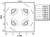
5A is a contour plot of the luminance of a dark field image from an optical system that does not include discrete retarder sections.
5B is a contour plot of the luminance of a dark field image from an optical system that includes discrete retarder sections.
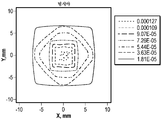
5C is a contour plot of the brightness of a bright field image from an optical system that does not include discrete retarder sections.
5D is a contour plot of the luminance of a bright field image from an optical system that includes discrete retarder sections.
6 is a schematic cross-sectional view of a simulated optical system for transmitting light.
7A is a schematic cross-sectional view of a simulated optical system for transmitting light.
7B is a schematic front view of a simulated optical element comprising discrete retarder segments on a quarter wave retarder.
본 발명의 원리에 따르면, 광학 시스템은 광학 디스플레이에서 콘트라스트를 개선하기 위한 광학 요소를 포함할 수 있다. 광학 요소는 사전결정된 파장의 광을 수신하도록 구성되는 광학 표면을 포함한다. 광학 요소는 균일한 지연의 광학 표면의 부분들 및 상이한 지연의 광학 표면의 부분들을 포함한다. 광학 요소는 광학 표면의 반대편 에지들을 가로질러 연장되는 제1 종방향 섹션 및 제2 종방향 섹션을 포함하고, 실질적으로 수직인 입사광에 대해 동일한 실질적으로 균일한 지연을 갖는다. 광학 요소는, 광학 표면 상에 각각 배치되는 그리고 0보다 큰, 종방향 섹션의 실질적으로 균일한 지연과의 지연 차이를 갖는 4개의 이산 지연기 섹션을 포함한다.According to the principles of the present invention, an optical system may include optical elements for improving contrast in an optical display. The optical element includes an optical surface that is configured to receive light of a predetermined wavelength. The optical element comprises parts of an optical surface of uniform retardation and parts of an optical surface of different retardation. The optical element includes a first longitudinal section and a second longitudinal section extending across opposite edges of the optical surface, and has substantially the same uniform delay for incident light that is substantially perpendicular. The optical element includes four discrete retarder sections, each disposed on an optical surface and having a delay difference from the substantially uniform delay of the longitudinal section, greater than zero.
전술된 광학 요소는 광학 시스템의 콘트라스트를 개선하기 위해 광학 시스템에 사용될 수 있다. 광학 시스템은, 각각이 하나 이상의 광학 렌즈의 적어도 하나의 주 표면 또는 다른 층 상에 배치되는, 반사 편광기 층, 부분 반사기 층, 제1 지연기 층, 제2 지연기 층, 및 제3 지연기 층을 포함할 수 있다. 부분 반사기와 반사 편광기는 그들 사이에 절첩된 광학 공동을 한정한다. 반사 편광기는 사전결정된 파장에서 제1 편광 상태를 갖는 광을 실질적으로 반사하고, 직교하는 제2 편광 상태를 갖는 광을 실질적으로 투과시킨다. 부분 반사기는 사전결정된 파장에서 적어도 30%의 평균 광학 반사율을 갖는다. 제1 지연기 층은 절첩된 광학 공동 내에 배치되는 한편, 제2 지연기 층 및 제3 지연기 층은 절첩된 광학 공동 외측에 배치된다. 제3 지연기 층은 전술된 광학 요소를 포함한다.The optical elements described above can be used in optical systems to improve the contrast of the optical system. The optical system includes a reflective polarizer layer, a partial reflector layer, a first retarder layer, a second retarder layer, and a third retarder layer, each disposed on at least one major surface or other layer of one or more optical lenses. It may include. The partial reflector and reflective polarizer define an optical cavity that is folded between them. The reflective polarizer substantially reflects light having a first polarization state at a predetermined wavelength, and substantially transmits light having an orthogonal second polarization state. The partial reflector has an average optical reflectance of at least 30% at a predetermined wavelength. The first retarder layer is disposed within the folded optical cavity, while the second retarder layer and the third retarder layer are disposed outside the folded optical cavity. The third retarder layer comprises the optical element described above.
본 발명에 따르면, 불균일한 지연을 갖는 광학 요소가 일부 광학 시스템에 존재하는 다양한 광학 결함을 보정하여 그에 따라서 개선된 광학 성능을 제공하는 데 사용될 수 있다. 파장판 및 반사 편광기와 같은 광학 시스템 내의 편광 구성요소는, 예를 들어 편광 구성요소의 제조 변동 또는 사각(oblique angle)으로 편광 구성요소에 입사하는 광에 대한 편광 구성요소의 거동 변동을 통해, 광학 시스템에서 오차 및 오정렬을 야기할 수 있다. 예를 들어, 표준 1/4 파장 지연기를 사용하는 광학 시스템에서, 반사 편광기의 국소 차단 상태와 반사 편광기에 첫 번째로 입사하는 광선의 편광 상태 사이에 그리고/또는 반사 편광기의 국소 통과 상태와 반사 편광기에 두 번째로 입사하는 광선의 편광 상태 사이에 오정렬이 있을 수 있다. 그러한 오정렬은, 예를 들어, 반사 편광기가 만곡된 형상으로 형성될 때 반사 편광기의 국소 통과 축 및 차단 축의 시프트로 인해 발생할 수 있다. 다른 예로서, 디스플레이와 같은 광원이 실질적으로 시준되지 않는 광을 생성하는 광학 시스템에서, 높은 입사각의 광선이 하나 이상의 1/4 파장 지연기의 표면으로부터 부분적으로 흡수되거나 투과될 수 있어서, 콘트라스트가 감소되게 할 수 있다.According to the present invention, optical elements with non-uniform delay can be used to correct for various optical defects present in some optical systems and thus provide improved optical performance. Polarization components in optical systems such as waveplates and reflective polarizers are optical, for example, through manufacturing variations of polarization components or through variations in the behavior of polarization components with respect to light entering the polarization component at an oblique angle. This can cause errors and misalignment in the system. For example, in an optical system using a standard quarter-wave retarder, between the local blocking state of the reflective polarizer and the polarization state of the first incident light to the reflective polarizer and/or the local passing state of the reflective polarizer and the reflective polarizer. There may be misalignment between the polarization states of the second incident light rays. Such misalignment can occur, for example, due to the shift of the local pass axis and the cut off axis of the reflective polarizer when the reflective polarizer is formed into a curved shape. As another example, in an optical system where a light source, such as a display, produces light that is not substantially collimated, high incident angle light rays can be partially absorbed or transmitted from the surface of one or more quarter wave retarders, thereby reducing contrast. I can do it.
본 발명에 따르면, 불균일한 지연을 갖는 광학 요소는 광학 시스템으로 들어가는 광을 지연시킬 수 있어서, 광학 시스템을 통해 전파되고 광학 시스템의 출구와 연관된 편광 구성요소의 표면 상에 입사하는 광선이 편광을 위한 원하는 편광 상태와 더 근사하게 매칭될 수 있게 할 수 있다. 예를 들어, 광축을 따라 이동하는 광선이 반사 편광기의 표면에 수직으로 입사할 때 실질적으로 차단되거나 투과될 수 있지만, 반사 편광기의 표면에 비스듬히 입사하는 광선은 차단 상태에 대해 반사 편광기를 통해 부분적으로 투과되고 통과 상태에 대해 반사 편광기 층으로부터 부분적으로 반사될 수 있으며, 이는 광학 시스템의 콘트라스트를 감소시킬 수 있다. 공간적으로 변화하는 불균일한 지연을 사용하여 광 누출을 보상하도록 구성되는 광학 요소를 포함함으로써, 광학 시스템의 콘트라스트가 증가될 수 있다. 광학 요소는 간단한 제조 기술을 사용하여 제조될 수 있다. 예를 들어, 1/4 파장 지연기와 같은 이산 지연기 섹션들이 광학 표면에 접착되어, 보상을 필요로 하는 광선과 연관된 광학 표면의 공간적 위치에서 불균일한 지연을 생성할 수 있다. 다른 예로서, 광학 요소는 기존의 광학 시스템에 추가될 수 있는 별개의 구성요소일 수 있어서, 광학 시스템이 상이한 광학 요소들로, 예를 들어 특정 시야를 갖는 특정 광원으로 재구성가능하게 될 수 있다.According to the present invention, an optical element having a non-uniform delay can delay light entering the optical system, such that light rays propagating through the optical system and incident on the surface of the polarization component associated with the exit of the optical system are used for polarization. It can be made to more closely match the desired polarization state. For example, light rays moving along the optical axis may be substantially blocked or transmitted when incident perpendicularly to the surface of the reflective polarizer, but light rays incident obliquely to the surface of the reflective polarizer may be partially through the reflective polarizer for the blocking state. It can be transmitted and partially reflected from the reflective polarizer layer for the pass state, which can reduce the contrast of the optical system. By including an optical element configured to compensate for light leakage using a spatially varying non-uniform delay, the contrast of the optical system can be increased. Optical elements can be manufactured using simple manufacturing techniques. For example, discrete retarder sections, such as quarter-wave retarders, can adhere to the optical surface, creating a non-uniform delay in the spatial location of the optical surface associated with the light beam in need of compensation. As another example, the optical element can be a separate component that can be added to an existing optical system, such that the optical system can be reconfigurable with different optical elements, for example a specific light source with a specific field of view.
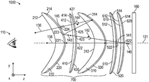
도 1은 광을 투과시키기 위한 광학 시스템(1000)의 개략적인 단면도이다. 광학 시스템(1000)은 광학 렌즈(210, 410, 310, 510, 610), 반사 편광기 층(220)(또한 "반사 편광기"로 지칭됨), 부분 반사기 층(320)(또한 "부분 반사기"로 지칭됨), 제1 지연기 층(420), 제2 지연기 층(520), 및 제3 지연기 층(620)(또한 각각 "제1 지연기", "제2 지연기", 및 "제3 지연기"로 지칭됨)을 포함한다.1 is a schematic cross-sectional view of an
도 1의 예에서, 물체(100)는 편광 상태(140)를 갖는 광선(136)을 방출한다. 제3 지연기 층(620)을 통과한 후에, 광선(136)은 편광 상태(141)를 갖고; 이어서, 제2 지연기 층(520) 및 부분 반사기 층(320)을 통과한 후에, 광선(136)은 편광 상태(142)를 가지며; 이어서, 제1 지연기 층(420)을 통과한 후에, 광선(136)은 반사 편광기 층(220)에 첫 번째로 입사할 때 편광 상태(143)를 갖고; 이어서, 제1 지연기 층(420)을 다시 통과하고 부분 반사기 층(320)으로부터 반사된 후에, 광선(136)은 편광 상태(144)를 가지며; 이어서, 광선(136)은 제1 지연기 층(420)을 통해 편광 상태(145)로 다시 통과하고, 반사 편광기 층(220)에 두 번째로 입사한다. 도 1은 또한 광선(138)을 개략적으로 예시한다. 광선(138)은 광축(121)을 따라 전파되고, 원점(522)에서 지연기 층(520)을 통과하며, 원점(422)에서 지연기 층(420)을 통과하고, 원점(221)에서 반사 편광기(220)를 통과한다. 편광 상태(140, 143)는 도 1에 도시된 x-y-z 좌표계를 참조하여, x-방향으로 편광된 전기장을 갖는 것으로 도 1에 개략적으로 도시되어 있다. 그러나, 이들 편광 상태 중 어느 하나 또는 둘 모두는 x-방향을 따라 선형 편광된 상태 이외의 어떤 상태일 수 있다. 예를 들어, 편광 상태(141)가 선형 편광되는 경우, 편광 상태(143)는 지연기 층(420, 520, 620)의 지연에 따라 타원 편광될 수 있다.In the example of FIG. 1,
광학 시스템(1000)의 구성요소는 광학 렌즈(210, 310, 410, 510, 610)의 하나 이상의 주 표면 상에 배치될 수 있다. 다른 실시 형태에서, 반사 편광기 층(220), 부분 반사기 층(320), 및 지연기 층(420, 520, 620) 중 하나 이상이 도 1에 예시된 실시 형태에 도시된 것과 상이한 주 표면 상에 배치된다. 예를 들어, 반사 편광기 층(220), 부분 반사기 층(320), 및 지연기 층(420, 520, 620) 중 임의의 하나 이상이 각각의 렌즈의 반대편 주 표면 상에 배치될 수 있다. 다른 예로서, 이들 층 중 하나 이상의 층이 이들 층 중 다른 하나의 층 상에 배치될 수 있다. 광학 렌즈(210)는 반대편 제1 및 제2 주 표면들(212, 214)을 갖고, 광학 렌즈(310)는 반대편 제1 및 제2 주 표면들(312, 314)을 가지며, 광학 렌즈(410)는 반대편 제1 및 제2 주 표면들(412, 414)을 갖고, 광학 렌즈(510)는 반대편 제1 및 제2 주 표면들(512, 514)을 가지며, 광학 렌즈(610)는 반대편 제1 및 제2 주 표면들(612, 614)을 갖는다.Components of the
광학 렌즈(210, 310, 410, 510, 610)는, 예를 들어, 아크릴 또는 유리와 같은 임의의 적합한 렌즈 재료로부터 제조될 수 있다. 일부 실시 형태에서, 광학 렌즈는 인서트 성형 공정(insert molding process)으로 형성된다. 예를 들어, 반사 편광기 층(220)이 원하는 형상으로 형성될 수 있고, 이어서, 광학 렌즈가 반사 편광기 층(220) 상에 인서트 성형될 수 있다. 임의의 유형의 적합한 렌즈(들)가 사용될 수 있다. 일부 실시 형태에서, 광학 시스템의 렌즈들 중 하나 이상은 평면-볼록 렌즈(plano-convex lens), 평면-오목 렌즈(plano-concave lens), 양면 볼록 렌즈(biconvex lens), 양면 오목 렌즈(biconcave lens), 정 메니스커스 렌즈(positive meniscus lens), 부 메니스커스 렌즈(negative meniscus lens), 가변 굴절률 렌즈(variable refractive index lens)(예컨대, 굴절률 분포형 렌즈(gradient-index lens)), 및 프레넬 렌즈(Fresnel lens) 중 하나이다. 추가의 광학 렌즈가 포함될 수 있고, 광학 렌즈(들)의 하나의 배열에 대해 기술된 속성들 중 많은 것이 광학 렌즈(들)의 다른 배열에 적용된다는 것이 이해될 것이다.The
광학 시스템(1000)은 광축(121)을 갖는다. 광학 시스템, 디스플레이 시스템, 또는 광학 시스템 내의 광학 렌즈 또는 광학 요소의 광축은, 광축을 따라 전파되는 광선이 최소 굴절도로 렌즈(들) 및/또는 광학 요소(들)를 통과하여, 광축에 가깝지만 광축과 상이한 축들을 따라 전파되는 광이 더 큰 굴절도를 겪도록 하는 시스템, 렌즈, 또는 광학 요소의 중심 부근의 축으로 이해될 수 있다. 일부 실시 형태에서, 하나 이상의 광학 렌즈(210, 310, 410, 510, 610) 각각은 하나 이상의 광학 렌즈(210, 310, 410, 510, 610) 각각의 정점을 통해 광축(121) 상에 중심설정된다. 광축(121)을 따른 광선은, 표면에 입사하는 광선과 표면을 통해 투과되는 광선 사이의 각도가 광학 시스템의 임의의 주 표면에서 15도 이하이도록, 굴절되거나 실질적으로 굴절됨이 없이 광학 렌즈(들) 및/또는 광학 요소(들)를 통과할 수 있다.The
일부 실시 형태에서, 광학 시스템(1000)은 물체(100)를 관찰자(110)에게 표시한다. 물체(100)는, 예를 들어, 디스플레이 또는 디스플레이 상의 이미지일 수 있다. 적합한 디스플레이는, 예를 들어, 액정 디스플레이(LCD) 및 유기 발광 다이오드(OLED) 디스플레이를 포함한다. 대안적으로, 물체(100)는 관찰자(110)의 환경 내의 물체와 같은 디스플레이 이외의 어떤 물체일 수 있다. 물체(100)가 디스플레이인 실시 형태에서, 디스플레이와 함께 광학 시스템(1000)은 디스플레이 시스템으로 지칭될 수 있거나, 또는 대안적으로, 광학 시스템(1000)은 디스플레이를 포함하는 것으로 기술될 수 있다. 일부 실시 형태에서, 물체(100)는 편광된 광 출력을 생성하는 디스플레이 패널이다. 일부 실시 형태에서, 광이 지연기 층(620)에 입사할 때 편광 상태(140)를 갖도록 물체(100)로부터의 광을 편광시키는 예비-편광기(pre-polarizer)가 제공된다. 일부 실시 형태에서, 물체(100)는 주변 광을 광학 시스템(1000)을 향해 반사시킴으로써 광(136)을 방출하는 관찰자(110)의 환경 내의 물체이다.In some embodiments,
광학 시스템(1000)은 반사 편광기 층(220)을 포함한다. 도 1의 예에서, 반사 편광기 층(220)은 광학 렌즈(210)의 주 표면(214) 상에 배치되고 그에 순응하지만; 다른 실시 형태에서, 반사 편광기 층(220)은 광학 시스템(1000)의 다른 주 표면 상에 배치될 수 있다.
반사 편광기 층(220)은 사전결정된 파장 또는 사전결정된 파장 범위에서 제1 편광 상태를 갖는 광을 실질적으로 반사하고, 직교하는 제2 편광 상태를 갖는 광을 실질적으로 투과시키도록 구성될 수 있다. 예를 들어, 반사 편광기 층(220)은, 사전결정된 파장에서 또는 사전결정된 파장 범위에서 제1 편광 상태를 갖는 광의 적어도 60%가 편광기로부터 반사되는 경우 사전결정된 파장에서 또는 사전결정된 파장 범위에서 제1 편광 상태를 갖는 광을 실질적으로 반사한다고 말할 수 있다. 반사 편광기 층(220)은, 사전결정된 파장에서 또는 사전결정된 파장 범위에서 제2 편광 상태를 갖는 광의 적어도 60%가 반사 편광기를 통해 투과되는 경우 사전결정된 파장에서 또는 사전결정된 파장 범위에서 제2 편광 상태를 갖는 광을 실질적으로 투과시킨다고 말할 수 있다.The
사전결정된 파장 범위는 광학 시스템 또는 디스플레이 시스템이 그에 걸쳐 동작하도록 설계되는 파장 범위일 수 있다. 사전결정된 파장은 약 400 nm 내지 약 1000 nm의 범위 내에 있을 수 있다. 예를 들어, 사전결정된 파장 범위는 가시 범위(400 nm 내지 700 nm)일 수 있다. 다른 예로서, 사전결정된 파장 범위는 하나 이상의 가시 파장 범위를 포함할 수 있다. 예를 들어, 사전결정된 파장 범위는 하나 초과의 좁은 파장 범위의 합집합(union)(예컨대, 디스플레이 패널의 발광 색에 대응하는 분리된 적색, 녹색 및 청색 파장 범위들의 합집합)일 수 있다. 그러한 파장 범위는 본 명세서에 참고로 포함되는 미국 특허 출원 공개 제2017/0068100호(Ouderkirk 등)에 추가로 기재되어 있다. 일부 실시 형태에서, 사전결정된 파장 범위는 다른 파장 범위(예컨대, 적외선(예컨대, 근적외선(약 700 nm 내지 약 2500 nm)), 또는 자외선(예컨대, 근자외선(약 300 nm 내지 약 400 nm)))뿐만 아니라 가시 파장 범위를 포함한다. 일부 예에서, 사전결정된 파장은 광학 시스템의 콘트라스트 비가 개선되는 파장일 수 있다. 예를 들어, 지연기 층(420, 520, 620)의 지연은 파장과 관련될 수 있어서, 지연기 층들(420, 520, 및/또는 620) 중 임의의 것에 대한 지연의 선택이 콘트라스트를 개선하게 할 수 있다.The predetermined wavelength range can be a wavelength range in which an optical system or display system is designed to operate across. The predetermined wavelength can be in a range of about 400 nm to about 1000 nm. For example, the predetermined wavelength range may be a visible range (400 nm to 700 nm). As another example, the predetermined wavelength range can include one or more visible wavelength ranges. For example, the predetermined wavelength range may be a union of more than one narrow wavelength range (eg, a combination of separate red, green and blue wavelength ranges corresponding to the emission color of the display panel). Such wavelength ranges are further described in US Patent Application Publication No. 2017/0068100 (Ouderkirk et al.), incorporated herein by reference. In some embodiments, the predetermined wavelength range is other wavelength range (eg, infrared (eg, near infrared (about 700 nm to about 2500 nm)), or ultraviolet light (eg, near ultraviolet (about 300 nm to about 400 nm))) As well as the visible wavelength range. In some examples, the predetermined wavelength can be a wavelength that improves the contrast ratio of the optical system. For example, the delay of the retarder layers 420, 520, 620 can be related to the wavelength, such that the choice of delay for any of the retarder layers 420, 520, and/or 620 improves contrast. can do.
본 명세서에 기술된 광학 시스템들 중 임의의 것에 사용되는 반사 편광기들 중 임의의 것은 제1 선형 편광 상태를 갖는 광을 반사하고 제1 선형 편광 상태에 직교하는 제2 선형 편광 상태를 갖는 광을 투과시키도록 구성될 수 있는 선형 반사 편광기일 수 있다. 적합한 반사 편광기는, 예를 들어, 중합체 다층 광학 필름 및 와이어-그리드 편광기를 포함한다. 본 발명의 광학 시스템들 중 임의의 것에 사용되는 반사 편광기들 중 임의의 것은 열성형된 중합체 다층 광학 필름일 수 있는 성형된(예컨대, 열성형된) 반사 편광기일 수 있다. 중합체 다층 광학 필름은 복수의 교번하는 제1 중합체 층 및 제2 중합체 층을 포함할 수 있다. 적합한 중합체 다층 반사 편광기는, 예를 들어, 미국 특허 제5,882,774호(Jonza 등), 및 미국 특허 제6,609,795호(Weber 등)에 기재되어 있다. 반사 편광기를 복합 곡선으로 형성하는 방법은 이전에 본 명세서에 참고로 포함된 미국 특허 출원 공개 제2017/0068100호(Ouderkirk 등), 및 2016년 9월 2일자로 출원되고 본 발명과 모순되지 않는 정도로 본 명세서에 참고로 포함되는 PCT 출원 제US2016/050024호(Ouderkirk 등)에 기재되어 있다.Any of the reflective polarizers used in any of the optical systems described herein reflect light having a first linear polarization state and transmit light having a second linear polarization state orthogonal to the first linear polarization state. It can be a linear reflective polarizer that can be configured to. Suitable reflective polarizers include, for example, polymeric multilayer optical films and wire-grid polarizers. Any of the reflective polarizers used in any of the optical systems of the present invention can be a shaped (eg, thermoformed) reflective polarizer that can be a thermoformed polymeric multilayer optical film. The polymer multilayer optical film can include a plurality of alternating first polymer layers and second polymer layers. Suitable polymeric multilayer reflective polarizers are described, for example, in US Pat. No. 5,882,774 (Jonza et al.), and US Pat. No. 6,609,795 (Weber et al.). The method of forming the reflective polarizer into a composite curve is to the extent that it is not inconsistent with the present invention filed on U.S. Patent Application Publication No. 2017/0068100 (Ouderkirk et al.), and September 2, 2016, previously incorporated herein by reference. It is described in PCT Application No. US2016/050024 (Ouderkirk et al.), incorporated herein by reference.
반사 편광기 층(220)은 중합체 다층 반사 편광기일 수 있고, 정점에서 실질적으로 일축 배향되는 적어도 하나의 층을 가질 수 있다. 일부 실시 형태에서, 반사 편광기 층(220)은 또한 적어도 하나의 층을 포함하는데, 적어도 하나의 층은, 광축으로부터 떨어진 적어도 하나의 층 상의 적어도 하나의 제1 위치에서 실질적으로 광학적으로 이축성이고, 광축으로부터 떨어진 적어도 하나의 제2 위치에서 실질적으로 광학적으로 일축성이다. 중합체 다층 광학 필름이 반사 편광기 층(220)을 제공하도록 성형(예컨대, 열성형)될 수 있다. 광학 필름은 초기에, y-방향을 따라 차단축과 일축 배향되는 적어도 하나의 층을 가질 수 있다. 성형 동안, 광학 필름은 공구의 형상에 순응하도록 연신된다. 광학 필름은 원하는 형상이 2개의 직교 축을 중심으로 만곡되기 때문에 연신된다. 이와 대조적으로, 광학 필름은 단지 하나의 축을 중심으로 만곡된 형상에 순응하기 위해 연신될 필요가 없을 것이다. 성형 공정은 광학 필름을 제1 위치에서 실질적으로 일축 배향된 상태로 남길 수 있지만(필름이 성형 동안 이러한 위치에서 배향 방향을 따라 연신되기 때문), 광학 필름이 성형될 때 광학 필름의 연신으로 인해 제2 위치에서 이축 배향을 유발할 수 있다.The
광학 시스템(1000)은 부분 반사기 층(320)을 포함할 수 있다. 도 1의 예에서, 부분 반사기 층(320)은 광학 렌즈(310)의 주 표면(314) 상에 배치되고 그에 순응하지만; 다른 예에서, 부분 반사기 층(320)은 광학 시스템(1000) 내의 다른 주 표면 상에 배치될 수 있다.The
부분 반사기 층(320)은 광학 시스템(1000)에 대한 임의의 적합한 반사율을 가질 수 있다. 일부 실시 형태에서, 부분 반사기 층(320)은 각각 30% 내지 70%의 범위 내에 있는, 사전결정된 파장에서의 또는 사전결정된 파장 범위에서의 평균 광학 반사율 및 평균 광학 투과율을 갖는다. 예를 들어, 부분 반사기 층(320)은 하프 미러(half mirror)일 수 있다. 사전결정된 파장 범위에서의 평균 광학 반사율 및 평균 광학 투과율은 각각, 달리 지시되지 않는 한 수직 입사에서 결정되는, 광학 반사율 및 광학 투과율의 사전결정된 파장 범위에 걸친 그리고 편광에 대한 비가중 평균을 지칭한다. 사전결정된 파장에서의 평균 광학 반사율 및 평균 광학 투과율은 각각, 달리 지시되지 않는 한 수직 입사에서 결정되는, 광학 반사율 및 광학 투과율의 편광에 대한 비가중 평균을 지칭한다.The
부분 반사기 층(320)은 임의의 적합한 부분 반사기일 수 있다. 예를 들어, 부분 반사기 층(320)은 투명 기재(예컨대, 후속하여 렌즈에 접착될 수 있는 필름, 또는 기재가 렌즈일 수 있음) 상에 금속(예컨대, 은 또는 알루미늄)의 얇은 층을 코팅함으로써 구성될 수 있다. 부분 반사기 층(320)은, 또한, 예를 들어, 렌즈 기재의 표면 상에 박막 유전체 코팅을 침착시킴으로써, 또는 표면 상에 금속 코팅과 유전체 코팅의 조합을 침착시킴으로써 형성될 수 있다. 일부 실시 형태에서, 부분 반사기 층(320)은 반사 편광기일 수 있거나, 편광 의존적 반사율을 가질 수 있다. 일부 예에서, 부분 반사기 층(320)은 유전체 부분 반사기 층이다.The
반사 편광기 층(220) 및 부분 반사기 층(320)은 절첩된 광학 공동(700)을 한정할 수 있다. 절첩된 광학 공동(700)은, 반사 편광기 층(220) 또는 부분 반사기 층(320) 중 어느 하나에서 제1 편광 상태의 광을 수신하고, 반사 편광기 층(220) 및 부분 반사기 층(320) 각각의 표면에서 광을 반사하며, 광이 수신되었던 반사 편광기 층(220) 또는 부분 반사기 층(320) 중 다른 하나로부터 제1 편광 상태의 광을 투과시키도록 구성될 수 있다. 반사 편광기 층(220) 및 부분 반사기 층(320) 둘 모두로부터 광을 반사함으로써, 광 경로가 제1 방향으로 압축(즉, "절첩")되거나 반대 제2 방향으로 압축되지 않을 수 있고, 절첩된 광학 공동(700)의 크기가 감소될 수 있다. 일부 예에서, 절첩된 광학 공동은 반전될 수 있어서, 관찰자 및 물체(100)에 대한 반사 편광기 층(220) 및 부분 반사기 층(320)의 상대 위치가 도 1의 예시적인 광학 시스템(1000)으로부터 반전되게 할 수 있다.The
일부 예에서, 광학 시스템(1000)의 표면은 추가의 반사-방지 층을 포함할 수 있다. 예를 들어, 반사-방지 층은 광학 렌즈(210)의 제1 지연기 층(420), 제2 지연기 층(520), 및 제2 주 표면(212) 중 하나 상에 배치될 수 있다. 다른 예로서, 제1 지연기 층(420) 또는 제2 지연기 층(520) 중 어느 하나가 도 1에 도시된 것과 같은 독립형 광학 요소인 경우, 각각의 지연기 층의 표면 및 각각의 광학 렌즈(410 또는 510)의 제2 주 표면이 반사-방지 코팅으로 코팅될 수 있다.In some examples, the surface of
광학 시스템(1000)은 제1 지연기 층(420), 제2 지연기 층(520), 및 제3 지연기 층(620)(집합적으로 "지연기 층(420, 520, 620)"으로 지칭됨)을 포함할 수 있다. 도 1의 예에서, 제1 지연기 층(420)은 절첩된 광학 공동(700) 내의 광학 렌즈(410)의 주 표면(414) 상에 배치되고 그에 순응하며; 제2 지연기 층(520)은 절첩된 광학 공동(700) 외측의 광학 렌즈(510)의 주 표면(514) 상에 배치되고 그에 순응하며; 제3 지연기 층(620)은 절첩된 광학 공동(700) 외측의 광학 렌즈(610)의 주 표면(614) 상에 배치되고 그에 순응한다. 그러나, 다른 예에서, 지연기 층들(420, 520, 620) 중 임의의 것이 광학 시스템(1000) 내의 다른 주 표면 상에 배치될 수 있다. 예를 들어, 제1 지연기 층(420)은 주 표면(214) 반대편의 반사 편광기 층(220) 상에 배치될 수 있고/있거나, 제2 지연기 층(520) 및 제3 지연기 층(620)은 주 표면(314) 반대편의 부분 반사기 층(320) 상에 배치될 수 있다.The
일부 실시 형태에서, 지연기 층들(420, 520, 620) 중 임의의 것이 만곡된 주 표면 상에 배치될 수 있다. 일부 실시 형태에서, 만곡된 주 표면은 하나의 축을 중심으로 만곡되거나, 2개의 직교 축을 중심으로 만곡된다. 일부 실시 형태에서, 지연기 층들(420, 520, 620) 중 임의의 것은 실질적으로 평면형의 것일 수 있다. 실질적으로 평면형의 층은 그 층이 공칭적으로는 평면형이지만, 예를 들어 통상적인 제조 변화로 인해 어느 정도의 곡률을 가질 수 있거나, (예컨대, 디스플레이 패널에 있는) 이미지 표면으로부터 광학 시스템의 정지 표면까지의 거리의 적어도 10배의 곡률 반경을 가질 수 있음을 의미하는 것으로 이해될 수 있다. 일부 실시 형태에서, 제3 지연기 층(620)은 디스플레이 패널 상에, 또는 광출력(optical power)을 갖지 않는 평면형 기재 상에 배치된다.In some embodiments, any of the retarder layers 420, 520, 620 can be disposed on a curved major surface. In some embodiments, the curved major surface is curved around one axis, or around two orthogonal axes. In some embodiments, any of the retarder layers 420, 520, 620 may be substantially planar. A substantially planar layer is a stationary surface of the optical system, although the layer is nominally planar, but may have some degree of curvature, for example due to typical manufacturing changes, or from an image surface (eg, in a display panel). It can be understood to mean that it can have a radius of curvature of at least 10 times the distance to. In some embodiments, the third retarder layer 620 is disposed on the display panel, or on a planar substrate that does not have optical power.
일부 경우에, 지연기 층들(420, 520, 620) 중 임의의 것은, 예를 들어, 다수의 층이 상이한 진상축(fast axis) 및 지상축(slow axis)을 갖는 다수의 적층된 지연기 층을 포함할 수 있다. 이러한 경우에, 지연기 층의 유효 지연 및 유효 진상축과 지상축은, 지연기에 입사하는 편광된 광 및 지연기를 통해 투과되는 편광된 광에 대해, 입사광의 편광 상태를 투과된 광의 편광 상태로 변환시킬 종래의 단일 층 지연기의 지연 및 진상축과 지상축 배향으로서 정의될 수 있다. 그러한 지연기 층의 지연은 이러한 유효 지연을 지칭한다. 단일 층을 갖는 지연기의 경우, 유효 광학 진상축과 지상축은 단일 층의 광학 진상축과 지상축이며, 유효 지연은 단일 층의 지연이다. 각각의 층이 지연기의 유효 진상축과 지상축에 평행하거나 그에 대해 90도만큼 회전된 진상축과 지상축을 갖는 다수의 층을 갖는 지연기 층의 경우, 수직 입사광에 대한 유효 지연은, 각각의 진상축과 지상축이 지연기의 유효 진상축과 지상축에 평행한 층들의 지연의 합에서 각각의 진상축과 지상축이 지연기의 유효 진상축과 지상축에 대해 90도만큼 회전된 층들의 지연의 합을 뺀 것이다.In some cases, any of the retarder layers 420, 520, 620, for example, multiple stacked retarder layers in which multiple layers have different fast and slow axes It may include. In this case, the effective delay and effective axis of retardation and the slow axis of the retarder layer convert the polarization state of the incident light to the polarization state of the transmitted light for polarized light incident on the retarder and polarized light transmitted through the retarder. It can be defined as the delay and the true axis and slow axis orientation of a conventional single layer retarder. The delay of such a delay layer refers to this effective delay. In the case of a retarder having a single layer, the effective optical advancing axis and slow axis are the single layer optical advancing axis and slow axis, and the effective delay is the single layer delay. In the case of a retarder layer in which each layer has multiple layers with a retardation axis and a retardation axis that are parallel to or rotated by 90 degrees to the effective reversal axis and retardation axis of the retarder, the effective retardation for vertical incident light is The effective axis of the retarder and the retardation of the layers parallel to the slow axis, respectively, in the sum of the retardation axis and the slow axis. It is the sum of the delays.
광학 시스템(1000)에 사용되는 지연기 층(들)은 필름 또는 코팅 또는 필름과 코팅의 조합일 수 있다. 적합한 필름은, 예를 들어, Meadowlark Optics(미국 콜로라도주 프레데릭 소재)로부터 입수가능한 것과 같은 복굴절 중합체 필름 지연기를 포함한다. 지연기 층을 형성하기 위한 적합한 코팅은 미국 특허 출원 공개 제2002/0180916호(Schadt 등), 제2003/028048호(Cherkaoui 등), 제2005/0072959호(Moia 등) 및 제2006/0197068호(Schadt 등)와 미국 특허 제6,300,991호(Schadt 등)에 기재된 선형 광중합성 중합체(LPP) 재료 및 액정 중합체(LCP) 재료를 포함한다. 적합한 LPP 재료는 ROP-131 EXP 306 LPP를 포함하고, 적합한 LCP 재료는 ROF-5185 EXP 410 LCP를 포함하며, 이들 둘 모두는 ROLIC Technologies Ltd.(스위스 알슈빌 소재)로부터 입수가능하다.The retarder layer(s) used in the
제1 지연기 층(420) 및 제2 지연기 층(520)은 각각 사전결정된 파장, 예를 들어 반사 편광기 층(220)의 맥락에서 논의된 사전결정된 파장에서 실질적으로 균일한 지연을 가질 수 있다. 지연기 층 또는 지연기 층 세그먼트는 지연기 층에서의 지연의 변화가 지연기에 걸친 지연의 최대 차이보다 실질적으로 더 작은 경우 실질적으로 균일한 지연을 갖는 것으로 기술될 수 있다. 예를 들어, 실질적으로 균일한 지연을 갖는 지연기는 지연의 최대 차이가 20% 이하임을 의미하는 것으로 이해될 수 있다.The
일부 예에서, 제1 지연기 층(420) 및 제2 지연기 층(520) 각각은 실질적으로 1/4 파장 지연기일 수 있다. 특정 파장에서 실질적으로 1/4 파장 지연기로 기술되는 지연기 층은, 지연기 층이 지연기 층의 표면적의 적어도 80%에 대해 수직으로 입사하는 비편광된 광에 대해 특정 파장의 1/4의 5% 내의 지연을 가짐을 의미하는 것으로 이해될 수 있다. 지연기 층은 제1 파장에서 실질적으로 1/4 파장 지연기일 수 있고, 상이한 제2 파장에서 1/4 파장과는 실질적으로 상이한 지연을 가질 수 있다. 제2 파장에서 1/4 파장과는 실질적으로 상이한 지연은 지연이 제2 파장의 1/4의 5% 내에 있지 않음을 의미하는 것으로 이해될 수 있다. 1/4 파장 지연기는 공간적으로 균일한 배향을 가질 수 있다.In some examples, each of the
일부 예에서, 지연기 층(420, 520)은 실질적으로 균일한 광학 두께를 갖는다. 예를 들어, 지연기 층(420, 520)은 실질적으로 동일한 지연을 제공하도록 동일한 재료로부터 구성될 수 있다. 일부 예에서, 지연기 층(520)은 지연기 층(420)과는 상이한 물리적 두께를 갖는다. 상이한 물리적 두께들을 이용하는 것은 지연기 층 각각이 대략 1/4 파장 지연을 갖기 위해 상이한 재료들이 상이한 지연기 층들에 사용될 때 바람직할 수 있다.In some examples, retarder layers 420 and 520 have a substantially uniform optical thickness. For example, retarder layers 420 and 520 can be constructed from the same material to provide substantially the same delay. In some examples,
제3 지연기 층(620)은 불균일한 지연을 가질 수 있다. 지연기 층은 지연기 층의 지연의 변화가 전술된 균일한 지연과 같은 균일한 지연을 나타내는 지연의 최대 차이보다 큰 경우 실질적으로 불균일한 지연을 갖는 것으로 기술될 수 있다. 예를 들어, 실질적으로 불균일한 지연을 갖는 지연기 층은 지연기 층에서의 지연의 최대 차이가 20% 초과임을 의미하는 것으로 이해될 수 있다.The third retarder layer 620 may have a non-uniform delay. The retarder layer can be described as having a substantially non-uniform delay when the change in the delay of the retarder layer is greater than the maximum difference in delay representing a uniform delay, such as the uniform delay described above. For example, a retarder layer with a substantially non-uniform delay can be understood to mean that the maximum difference in delay in the retarder layer is greater than 20%.
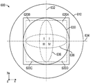
일부 예에서, 제3 지연기 층(620)은 제3 지연기 층(620)에서 불균일한 지연을 생성하기 위해 이산 지연기 섹션들을 포함할 수 있다. 제3 지연기 층(620)이 전체적으로 불균일한 지연을 가질 수 있지만, 각각의 이산 지연기 섹션은 이산 지연기 섹션에 걸쳐 균일한 지연을 가질 수 있다. 도 2는 이산 지연기 섹션들을 포함하는, 도 1의 제3 지연기 층(620)과 같은 광학 요소(600)의 개략적인 정면도이다.In some examples, the third retarder layer 620 may include discrete retarder sections to create a non-uniform delay in the third retarder layer 620. Although the third retarder layer 620 may have an overall non-uniform delay, each discrete retarder section may have a uniform delay across the discrete retarder section. 2 is a schematic front view of an optical element 600, such as the third retarder layer 620 of FIG. 1, including discrete retarder sections.
광학 요소(600)는 반사 편광기 층(220)의 맥락에서 기술된 사전결정된 파장과 같은 사전결정된 파장의 광을 수신하도록 구성되는 광학 표면(630)을 포함한다. 광학 표면(630)은 광학 렌즈, 파장판 등과 같은 광학 요소의 다양한 표면을 포함할 수 있다. 일부 예에서, 광학 표면(630)은 광학 요소의 전체 표면으로 연장될 수 있는 한편, 다른 예에서, 광학 표면(630)은 이미지와 연관된 광을 수신하는 광학 요소의 주 표면의 부분과 같은 광학 요소의 일부분으로 제한될 수 있다. 일부 예에서, 사전결정된 파장은 약 400 nm 내지 약 1000 nm의 범위 내에 있을 수 있다. 광학 표면(630)은 수직축(632) 및 수평축(634)에 의해 한정될 수 있다. 수직축(632) 및 수평축(634)은 4개의 직교 사분면(I, II, III, IV)을 한정할 수 있다. 도 2의 예에서, 직교 사분면은 반시계 방향으로 순차적으로 번호가 부여된다.Optical element 600 includes an
광학 표면(630)은 수직축(632) 상에 실질적으로 중심설정되는 제1 종방향 섹션(636) 및 수평축(634) 상에 실질적으로 중심설정되는 제2 종방향 섹션(638)을 포함할 수 있다. 제1 종방향 섹션(636) 및 제2 종방향 섹션(638)은 각각 광학 표면의 반대편 에지들을 가로질러 연장될 수 있다. 제1 종방향 섹션(636) 및 제2 종방향 섹션(638)은 보상을 필요로 하지 않을 수 있는 광선을 수신하도록 구성되는 광학 요소(600)의 일부분을 나타낼 수 있다. 예를 들어, 제1 종방향 섹션(636), 제2 종방향 섹션(638), 또는 둘 모두에 입사하는 광선은 그가 광학 시스템(1000) 내에서의 오정렬에 의해 실질적으로 영향을 받지 않도록 광학 시스템(1000)을 통해 전파될 수 있다.The
제1 종방향 섹션(636) 및 제2 종방향 섹션(638)은 실질적으로 수직인 입사광에 대해 동일한 실질적으로 균일한 지연(δ)을 가질 수 있다. 실질적으로 균일한 지연은, 제1 및 제2 종방향 섹션들(636, 638) 각각에서의 지연의 최대 변화(그 영역에서의 최대 지연 빼기 최소 지연)가 각각의 종방향 섹션에서의 지연의 최대 변화의 10% 이하일 수 있음을 의미하는 것으로 이해될 수 있다. 광학 표면(630)이 광학 렌즈의 표면인 예에서, 실질적으로 균일한 지연은 0일 수 있다. 광학 표면(630)이 제2 지연기 층(520)과 같은 1/4 파장 지연기의 표면인 예에서, 실질적으로 균일한 지연은 제2 지연기 층(520)의 1/4 파장 지연일 수 있다. 일부 예에서, 제1 및 제2 종방향 섹션들(636, 638)은 광학 표면(630)의 표면적의 적어도 10%를 덮는다.The first
제3 지연기 층(620)은 복수의 이산 지연기 섹션을 포함할 수 있다. 이산 지연기 섹션은 광학 표면(630)의 이산 섹션을 덮는 지연기 섹션일 수 있다. 일부 예에서, 복수의 이산 지연기 섹션은 물리적으로 이산될 수 있어서, 2개의 지연기 섹션이 물리적으로 접촉하지 않게 한다. 일부 예에서, 복수의 이산 지연기 섹션들 중 2개 이상이 물리적으로 접촉하거나 결합될 수 있지만, 광학 표면(630)의 이산 부분들을 덮을 수 있다.The third retarder layer 620 may include a plurality of discrete retarder sections. The discrete retarder section can be a retarder section that covers the discrete section of the
도 2의 예에서, 제3 지연기 층(620)은 제1 지연기 섹션(620A), 제2 지연기 섹션(620B), 제3 지연기 섹션(620C), 및 제4 지연기 섹션(620D)을 포함하는, 4개의 이산 지연기 섹션을 포함한다. 각각의 이산 지연기 섹션(620A, 620B, 620C, 620D)은 광학 표면(630)의 각각의 직교 사분면(I, II, III, IV) 상에 배치될 수 있다.In the example of FIG. 2, the third retarder layer 620 includes a
각각의 이산 지연기 섹션은 0보다 큰, 제1 및 제2 종방향 섹션들(626, 628)의 실질적으로 균일한 지연(δ)과의 지연 차이(θ)를 가질 수 있다. 일부 예에서, 각각의 이산 지연기 섹션(620A, 620B, 620C, 620D)은 제1 및 제2 종방향 섹션들(626, 628)의 실질적으로 균일한 지연과의 실질적으로 균일한 지연 차이를 갖는다. 예를 들어, 각각의 이산 지연기 섹션(620A, 620B, 620C, 620D)은 제1 및 제2 종방향 섹션들(626, 628)의 지연과의 약 0.2λ의 지연 차이를 가질 수 있다.Each discrete retarder section can have a delay difference [theta] with a substantially uniform delay δ of the first and second
일부 예에서, 이산 지연기 섹션들의 지연 차이는 고스트 이미지(ghost image), 콘트라스트 비, 광 누출, 출력 등을 포함하지만 이에 제한되지 않는 다수의 인자에 따라 선택될 수 있다. 예를 들어, 도 4a 내지 도 4c에 알 수 있는 바와 같이, 콘트라스트 및 암시야 광 누출은 이산 지연기 섹션들의 지연 차이가 증가함에 따라 증가할 수 있지만, 명시야에 대한 출력은 감소할 수 있다. 특정 응용의 경우, 광 누출의 감소 및 콘트라스트의 증가는, 예를 들어 명시야 밝기의 감소와 균형을 이룰 수 있다. 일부 예에서, 지연 차이는 약 0.2λ 미만이다. 예를 들어, 0.2λ는 유리하게는 충분한 출력 및/또는 밝기를 유지시키면서 개선된 콘트라스트와 연관될 수 있다. 일부 예에서, 지연 차이는 약 0.1λ 미만일 수 있다. 예를 들어, 0.1λ는 유리하게는 작은 시야를 갖는 절첩된 광학 시스템(folded optical system)에 대한 개선된 콘트라스트와 연관될 수 있다.In some examples, the delay difference of the discrete retarder sections can be selected according to a number of factors, including but not limited to ghost image, contrast ratio, light leakage, output, and the like. For example, as can be seen in FIGS. 4A-4C, contrast and dark field light leakage may increase as the delay difference in the discrete retarder sections increases, but output to the bright field may decrease. For certain applications, a reduction in light leakage and an increase in contrast can be balanced with, for example, a decrease in bright field brightness. In some examples, the delay difference is less than about 0.2λ. For example, 0.2λ can be advantageously associated with improved contrast while maintaining sufficient output and/or brightness. In some examples, the delay difference may be less than about 0.1λ. For example, 0.1λ can advantageously be associated with improved contrast for a folded optical system with a small field of view.
지연 차이(θ)는 양의 지연 차이(θ+) 또는 음의 지연 차이(θ-)일 수 있다. 이산 지연기 섹션이 양의 지연 차이를 포함하는지 또는 음의 지연 차이를 포함하는지는 광학 시스템(1000)을 통한 광의 원하는 편광 상태에 의존할 수 있다. 예를 들어, 제3 지연기 층(620)의 특정한 이산 지연기 섹션은 시계 방향 타원 편광이 요구되는 경우 양의 지연 차이를 가질 수 있고, 반시계 방향 타원 편광이 요구되는 경우 음의 지연 차이를 가질 수 있다. 일부 예에서, 제3 지연기 층(620)의 2개의 이산 지연기 섹션은 제1 및 제2 종방향 섹션들(636, 638)의 지연(δ)과의 양의 지연 차이(θ+)를 가질 수 있고, 제3 지연기 층(620)의 2개의 다른 이산 지연기 섹션은 제1 및 제2 종방향 섹션들(636, 638)의 지연(δ)과의 음의 지연 차이(θ-)를 가질 수 있다. 예를 들어, 제1 및 제3 이산 지연기 섹션들(620A, 620C)은 제1 및 제2 종방향 섹션들(636, 638)의 지연과의 +0.2λ의 지연 차이를 가질 수 있고, 제2 및 제4 이산 지연기 섹션들(620B, 620D)은 제1 및 제2 종방향 섹션들(636, 638)의 지연과의 -0.2λ의 지연 차이를 가질 수 있거나, 또는 그 반대일 수 있다.The delay difference θ may be a positive delay difference θ+ or a negative delay difference θ-. Whether the discrete retarder section includes a positive delay difference or a negative delay difference may depend on the desired polarization state of light through the
지연은 특정한 이산 지연기 섹션(620A, 620B, 620C, 620D), 또는 종방향 섹션(636, 638)에 대한 평균 지연을 의미할 수 있다는 것이 이해될 것이다. 예를 들어, 특정 파장에 대해, 제1 및 제2 종방향 섹션들(636, 638)은 δ와 실질적으로 동일한 평균 지연을 가질 수 있는 한편, 각각의 이산 지연기 섹션(620A, 620B, 620C, 620D)은 예를 들어 제2 및 제4 이산 지연기 섹션들(620B, 620D)에 대해, θ+와 실질적으로 동일한 평균 지연, 또는 예를 들어 제1 및 제3 이산 지연기 섹션들(620A, 620C)에 대해, θ-와 실질적으로 동일한 평균 지연을 가질 수 있다.It will be understood that the delay can mean the average delay for specific
제3 지연기 층(620)의 지연은 광학 두께와 상관될 수 있다. 특정 유효 광학 진상축 또는 지상축에 대한 지연기 층의 광학 두께는 특정 유효 광학 진상축 또는 지상축을 따른 층의 굴절률에 층의 두께를 곱한 것의 지연기의 각각의 층에 걸친 합을 지칭한다. 일부 예에서, 제1 및 제2 종방향 섹션들(636, 638) 각각은 동일한 실질적으로 균일한 광학 두께(Λ)를 갖는다. 일부 예에서, 이산 지연기 섹션 각각은 0보다 큰, 제1 및 제2 종방향 섹션들(636, 638)의 실질적으로 균일한 광학 두께(Λ)와의 광학 두께 차이(ε)를 갖는다. 일부 예에서, 제3 지연기 층(620)의 2개의 이산 지연기 섹션은 제1 및 제2 종방향 섹션들(636, 638)의 광학 두께(Λ)와의 양의 광학 두께 차이(ε+)를 가질 수 있고, 제3 지연기 층(620)의 2개의 다른 이산 지연기 섹션은 제1 및 제2 종방향 섹션들(636, 638)의 광학 두께(Λ)와의 음의 광학 두께 차이(ε-)를 가질 수 있다.The delay of the third retarder layer 620 may be correlated with the optical thickness. The optical thickness of the retarder layer for a particular effective optical axis or slow axis refers to the sum over each layer of the retarder by multiplying the layer thickness by the refractive index of the layer along the specific effective optical axis or slow axis. In some examples, each of the first and second
이산 지연기 섹션들(620A, 620B, 620C, 620D)의 상대 크기는 광축에 직교하는 평면으로부터의 평면도에서 결정되는 바와 같은 광학 표면(630)의 표면적의 관점에서 기술될 수 있다. 일부 실시 형태에서, 평면도에서, 광학 표면(630)은 면적 A를 가져서, 이산 지연기 섹션들(620A, 620B, 620C, 620D)이 약 A/10 내지 약 2A/3의 범위 내의 조합 면적을 갖고, 이산 지연기 섹션들(620A, 620B, 620C, 620D) 각각이 약 A/40 내지 약 A/6의 범위 내의 면적을 갖게 한다. 일부 예에서, 각각의 이산 지연기 섹션(620A, 620B, 620C, 620D)은 광학 표면(630)의 각각의 직교 사분면(I, II, III, IV)의 표면적의 적어도 20%를 덮는다. 일부 예에서, 이산 지연기 섹션들(620A, 620B, 620C, 620D)의 표면 커버리지(surface coverage)는 디스플레이(880)의 시야와 관련될 수 있어서, 시야가 증가함에 따라, 이산 지연기 섹션들(620A, 620B, 620C, 620D) 각각의 표면 커버리지가 증가하게 한다.The relative size of the
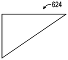
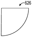
제3 지연기 층(620)의 이산 지연기 섹션들은 다양한 형상을 가질 수 있다. 도 3a 내지 도 3d는 다양한 형상을 갖는 이산 지연기 세그먼트들의 개략적인 정면도이다. 도 3a는 직각 및 정사각형 변들을 포함하는 직각 삼각형 형상을 갖는 이산 지연기 섹션(622)을 예시한다. 이산 지연기 섹션(622)은, 예를 들어, 정사각형 이미지를 수신하는 광학 표면에 사용될 수 있다. 도 3b는 직각 및 직사각형 변들을 포함하는 직각 삼각형 형상을 갖는 이산 지연기 섹션(624)을 예시한다. 이산 지연기 섹션(624)은, 예를 들어, 광각 이미지를 수신하는 광학 표면에 사용될 수 있다. 도 3c는 직각, 정사각형 변들, 및 원형 빗변을 포함하는 사분원호 형상(circle quadrant shape)을 갖는 이산 지연기 섹션(626)을 예시한다. 이산 지연기 섹션(626)은, 예를 들어, 만곡된 광학 표면에 사용될 수 있다. 도 3d는 직각, 정사각형 변들, 및 오목한 빗변을 포함하는 반전된 사분원호 형상을 갖는 이산 지연기 섹션(628)을 예시한다. 사용될 수 있는 다른 형상은 원, 정사각형, 삼각형 등을 포함하지만, 이에 제한되지 않는다. 예를 들어, 도 7b에 예시된 바와 같이, 사분면보다는 오히려 전체 형상이 사용될 수 있다. 이산 지연기 섹션들(620A, 620B, 620C, 620D)의 형상을 선택하기 위해 사용될 수 있는 인자는 시야, 디스플레이(100)의 형상, 광의 입사각 등을 포함할 수 있지만, 이에 제한되지 않는다.Discrete retarder sections of the third retarder layer 620 may have various shapes. 3A-3D are schematic front views of discrete retarder segments having various shapes. 3A illustrates a
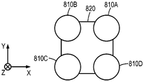
일부 실시 형태에서, 이산 지연기 섹션들(620A, 620B, 620C, 620D)은 광학 표면(630)의 주연부를 실질적으로 덮도록 형상화될 수 있다. 이산 지연기 섹션들(620A, 620B, 620C, 620D)은, 이산 지연기 섹션들(620A, 620B, 620C, 620D)이 광학 표면(630)의 주연부의 적어도 50%를 덮는 경우 광학 표면(630) 주위의 주연부를 실질적으로 덮는다고 말할 수 있다. 예를 들어, 도 2의 예에서, 이산 지연기 섹션들(620A, 620B, 620C, 620D)은 광학 표면(630)의 주연부의 적어도 80%를 덮는 한편, 후술되는 도 7b의 예에서, 이산 지연기 섹션들(810A, 810B, 810C, 810D)은 제2 지연기 층(820)의 주연부의 약 70%를 덮는다.In some embodiments, the
하나의 광학 시스템에 대해 기술된 광학 요소(600)의 특성들(예컨대, 이산 지연기 섹션들을 통한 불균일한 지연)이, 또한, 광학 시스템에 대응하지만 상이한 개수의 광학 렌즈를 갖거나 하나 이상의 광학 렌즈의 상이한 주 표면 상에 배치되는 다양한 층을 갖는 다른 광학 시스템에 적용된다는 것이 이해될 것이다. 제3 지연기 층(620)이 광학 요소(600)로서 광학 렌즈(610)의 광학 표면 상에 배치되는 것으로 기술되었지만, 제3 지연기 층(620)은 다양한 광학 표면 상에 배치될 수 있다. 예를 들어, 제3 지연기 층(620)은 제2 지연기 층(520)과 같은 지연기의 광학 표면 상에 배치될 수 있다. 일부 예에서, 제3 지연기 층(620)은 1/4 파장 지연기 상에 배치될 수 있어서, 제3 지연기 층(620) 및 1/4 파장 편광기가, 예를 들어, 절첩된 광학 공동(700)과 같은 절첩된 광학 공동과 함께 사용될 수 있게 할 수 있다.The properties of the optical element 600 described for one optical system (eg, non-uniform delay through discrete retarder sections) also correspond to the optical system but have different numbers of optical lenses or have one or more optical lenses It will be understood that it applies to different optical systems having various layers disposed on different major surfaces of the. Although the third retarder layer 620 has been described as being disposed on the optical surface of the
이산 지연기 섹션들(620A, 620B, 620C, 620D)은, 원자층 증착(atomic layer deposition), 접착, 및 광학 표면 상에 이산 지연기 섹션들을 형성할 수 있는 임의의 다른 기술을 포함하지만 이에 제한되지 않는 다양한 방법을 사용하여 광학 표면 상에 배치될 수 있다. 일부 예에서, 이산 지연기 섹션들은 광학 표면과 별도로 형성되고 광학 표면 상에 접착될 수 있다. 일부 예에서, 광학 요소(600)를 제조하기 위한 방법은, 광학 표면이 각각이 광학 표면(630)의 반대편 에지들을 가로질러 연장되고 실질적으로 수직인 입사광에 대해 동일한 실질적으로 균일한 지연(δ)을 갖는 제1 및 제2 종방향 섹션들(636, 638)을 포함하도록, 4개의 이산 지연기 섹션들(620A, 620B, 620C, 620D)을 광학 표면(630)에 결합시키는 단계를 포함한다. 예를 들어, 이산 지연기 섹션들은 지연 차이(θ)와 동일한 균일한 지연을 갖는 지연기 층으로서 형성되고 형상들로 처리될 수 있다. 이산 지연기 섹션들은 원하는 구성으로 광학 표면(630) 상에 위치될 수 있다. 예를 들어, 2개의 이산 지연기 섹션은 이러한 2개의 이산 지연기 섹션이 양의 지연 차이(θ+)를 갖도록 광학 표면(630)의 2개의 반대편 모서리들에 위치될 수 있는 한편, 2개의 다른 이산 지연기 섹션은 이러한 2개의 다른 이산 지연기 섹션이 음의 지연 차이(θ-)를 갖도록 광학 표면(630)의 2개의 다른 반대편 모서리들에 위치될 수 있다. 이산 지연기 섹션들은, 예를 들어 광학 접착제를 사용함으로써, 광학 표면(630)에 접착될 수 있다.
광학 요소(600)는 콘트라스트를 개선하기 위해 도 1의 광학 시스템(1000)과 같은 광학 시스템에 사용될 수 있다. 예를 들어, 물체(100)는 광학 시스템(1000)의 입력 단부를 한정할 수 있고, 사용자(110)는 광학 시스템(1000)의 출력 단부를 한정할 수 있다. 광학 시스템(1000)의 입력 단부에서 수신된 이미지는 광학 시스템(1000)의 출력 단부에서 검출될 수 있다. 광학 시스템(1000)의 출력 단부에서 검출된 이미지는 콘트라스트 변화를 가질 수 있다. 예를 들어, 도 5b 및 도 5d에서, 이미지(784B, 784D)는, 각각, 콘트라스트 비를 함께 한정하는 휘도의 변화를 가지며, 여기에서 콘트라스트는 명시야 휘도/암시야 휘도로 정의된다. 이미지(784D)의 명시야 휘도는 상당히 균일할 수 있지만, 이미지(784B)의 암시야 휘도는 매우 불균일하여서, 콘트라스트 변화가 크게 한다.The optical element 600 can be used in an optical system such as the
일부 예에서, 제3 지연기 층(620)은 이미지가 광학 시스템(1000)의 입력 단부에서 수신되고 광학 시스템(1000)의 출력 단부에서 검출될 때, 광학 시스템(1000)의 출력 단부에서의 이미지가 제3 지연기 층을 갖지 않는 비교 광학 시스템의 출력 단부에서 검출된 이미지보다 적어도 5% 더 작은 최대 콘트라스트 변화를 갖도록 구성될 수 있다. 예를 들어, 도 5a 및 도 5c에서, 이미지(784A, 784C)는, 각각, 콘트라스트 비를 한정하는 휘도의 변화를 갖는다. 도 5a 내지 도 5d의 예에서 알 수 있는 바와 같이, 제3 지연기 층(620)과 같은 보상 지연기 층은 밝은 상태에 있는 이미지의 부분들에 대한 휘도를 감소시킬 수 있지만, 보상 지연기 층은 어두운 상태에 있는 이미지의 부분들의 휘도를 상당히 감소시킬 수 있어서, 콘트라스트 변화가 보상 지연기 층(810)이 없는 비교 광학 시스템보다 작게 할 수 있다.In some examples, the third retarder layer 620 is an image at the output end of the
광학 요소(600)는 광학 시스템의 반사 편광기에 입사하는 광선의 반사율을 개선하기 위해, 도 1의 광학 시스템(1000)과 같은 광학 시스템에 사용될 수 있다. 예를 들어, 물체(100)로부터 방출된 광선(136)은 반사 편광기 층(220)에 첫 번째로 입사하고 제1 반사율(ρ)로 다시 실질적으로 반사될 수 있다. 광선(136)이 반사 편광기 층(220)에 두 번째로 입사할 때, 광선(136)은 제1 투과율(τ)로 실질적으로 투과될 수 있다.The optical element 600 can be used in an optical system, such as the
일부 예에서, 제3 지연기 층(620)은 사전결정된 파장에서 디스플레이로부터 방출된 이미지 광선이 반사 편광기에 첫 번째로 입사할 때, 이미지 광선이 제1 반사율(ρ)로 실질적으로 반사되고, 이미지 광선이 반사 편광기에 두 번째로 입사할 때, 이미지 광선이 제1 투과율(τ)로 실질적으로 투과되도록 구성될 수 있으며, 이때 제3 지연기 층은 제1 반사율을 증가시킨다. 전술된 바와 같이, 제3 지연기 층(620)은 광학 시스템에서 편광 상태의 위상 시프팅을 야기할 수 있는 오정렬을 보상할 수 있다. 제3 지연기 층(620)은 반사 편광기 층(220)에 첫 번째로 입사하는 광선이 반사 편광기 층(220)의 차단 상태와 더 정확하게 정렬될 수 있도록 광선을 위상 시프트시킬 수 있어서, 광선이 반사될 수 있고, 반사 편광기가 제3 지연기 층(620)을 갖지 않는 비교 광학 시스템보다 더 높은 반사율을 가질 수 있게 할 수 있다. 일부 예에서, 광학 시스템에 대한 제3 지연기 층(620)의 추가는 제1 투과율을 실질적으로 변화시키지 않는다. 예를 들어, 반사율은 증가할 수 있지만, 실질적으로 동일한 양의 광이 투과될 수 있다.In some examples, the third retarder layer 620 is when the image light beam emitted from the display at a predetermined wavelength first enters the reflective polarizer, the image light beam is substantially reflected at the first reflectance (ρ), and the image When the light beam enters the reflective polarizer a second time, the image light beam can be configured to be substantially transmitted at a first transmittance τ, where the third retarder layer increases the first reflectivity. As described above, the third retarder layer 620 may compensate for misalignment that may cause phase shifting of the polarization state in the optical system. The third retarder layer 620 may phase shift the light beam so that the light incident first to the
광학 요소(600)는 광학 시스템에서 원하지 않는 출력 편광의 광의 누출을 감소시키기 위해, 도 1의 광학 시스템(1000)과 같은 광학 시스템에 사용될 수 있다. 광의 누출의 감소는 광학 시스템을 통해 처리된 이미지의 편광 성분의 최대 세기의 감소에 의해 나타내어질 수 있다. 일부 예에서, 제3 지연기 층(620)은 균일하게 편광된 명시야 이미지가 광학 시스템(1000)에 입사하고 반사 편광기 층(220) 및 부분 반사기 층(320) 각각에서 적어도 한 번의 반사를 겪은 후에 광학 시스템(1000)을 빠져나갈 때, 출사 이미지 광이 출사 개구부를 충전할 수 있도록 구성될 수 있으며, 이때 개구부를 충전하는 이미지는 제1 편광 상태를 갖는 제1 이미지 성분을 갖고, 여기서 제1 이미지 성분의 최대 세기는 제3 지연기 층을 갖지 않는 비교 광학 시스템보다 적어도 10% 더 작다. 예를 들어, 도 4c는 도 7a의 보상 지연기 층(810)의 지연이 증가함에 따른 출력의 감소를 도시한다.The optical element 600 can be used in an optical system, such as the
실시예Example
실시예 1: 절첩된 광학 시스템 시뮬레이션Example 1: Folded optical system simulation
도 6은 광을 투과시키기 위한 모의 광학 시스템의 개략적인 단면도이다. 표면(720)은 발광 물체의 표면을 나타낼 수 있다. 광학 시스템을 통해 전파되는 광은 표면(730, 740, 750)을 통과하고, 표면(760)으로부터 반사되며, 표면(750)을 통과하고, 표면(740)으로부터 반사되며, 표면(750, 760)을 통과하고, 표면(770) 상에서 방출될 수 있다. 도 6의 광학 시스템은 아래의 표 1에 나타낸 바와 같이, 하기의 특성을 가질 수 있다:6 is a schematic cross-sectional view of a simulated optical system for transmitting light. The
[표 1][Table 1]

실시예 2: 이산 지연기 세그먼트들을 갖는 절첩된 광학 시스템을 사용한 광 누출 보상 시뮬레이션Example 2: Simulation of light leakage compensation using a folded optical system with discrete retarder segments
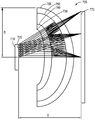
도 7a는 광을 투과시키기 위한 모의 광학 시스템(800)의 개략적인 단면도이다. 광학 시스템(800)은 제2 1/4 파장 지연기 층(820), 부분 반사기 층(830), 제1 1/4 파장 지연기 층(840), 반사 편광기 층(850), 디스플레이(880), 및 예비-편광기(890)를 포함한다. 광학 시스템(800)은 후술될 바와 같이, 시험 구성에 따라 보상 지연기 층(810) 및/또는 흡수 편광기(860)를 선택적으로 포함할 수 있다. 디스플레이(880)는 이미지(874)를 형성하기 위해 개구부(872)를 갖는 모의 눈(870)으로 광을 방출할 수 있다. 제1 1/4 파장 지연기 층(840), 제2 1/4 파장 지연기 층(820), 및 보상 지연기 층(810) 각각을 각각의 지연기 층에 걸쳐 실질적으로 균일한 지연을 갖고서 모델링하였다. 도 7a의 구성요소는 도 1의 유사한 구성요소에 대응할 수 있다. 예를 들어, 보상 지연기 층(810)은 제3 지연기 층(620)에 대응할 수 있고, 제2 1/4 파장 지연기 층(820)은 제2 지연기 층(520)에 대응할 수 있으며, 제1 1/4 파장 지연기 층(840)은 제1 지연기 층(420)에 대응할 수 있고, 부분 반사기 층(830)은 부분 반사기 층(320)에 대응할 수 있으며, 반사 편광기 층(850)은 반사 편광기 층(220)에 대응할 수 있고, 디스플레이(880) 및 예비-편광기(890)는 디스플레이(100)에 대응할 수 있다.7A is a schematic cross-sectional view of a simulated
흡수 편광기(860)는 이미지(874)에 대한 명시야 이미지 또는 이미지(874)에 대한 암시야 이미지를 생성하도록 구성될 수 있다. 예를 들어, 명시야 이미지 구성에서, 흡수 편광기(860)는 반사 편광기 층(850)으로부터 방출된 광의 편광 상태와 정렬될 수 있어서, 이미지(874)가 명시야 이미지이게 한다. 대안적으로, 흡수 편광기는 광학 시스템(800)으로부터 제거될 수 있다. 암시야 이미지 구성에서, 흡수 편광기(860)는 반사 편광기 층(850)으로부터 방출된 광의 편광 상태로부터 대략 90°로 교차되거나 오정렬될 수 있어서, 이미지(874)가 암시야 이미지이게 한다.The absorbing
보상 지연기 층(810)은, 보상된 또는 보상되지 않은 이미지를 각각 생성하는 보상된 또는 보상되지 않은 광학 시스템 각각에 대해 광학 시스템(800)에 포함되거나 그로부터 제거될 수 있다. 도 7b는 제2 1/4 파장 지연기 층(820)과 중첩되는 보상 지연기 층(810)의 개략적인 정면도이다. 보상 지연기 층(810)은 4개의 원형의 이산 지연기 섹션(810A, 810B, 810C, 810D)을 포함할 수 있다.The
광학 시스템(800)을 하기의 4가지 총 구성에 대한 보상 지연기 층(810) 및 흡수 편광기(860)의 상이한 구성들에서 시험하였다: 보상되지 않은 암시야 이미지(874A)에 대한, 흡수 편광기(860)가 있고 보상 지연기 층(810)이 없는 구성; 보상된 암시야 이미지(874B)에 대한, 흡수 편광기(860)가 있고 보상 지연기 층(810)이 있는 구성; 보상되지 않은 명시야 이미지(874C)에 대한, 흡수 편광기(860)가 없고 보상 지연기 층(810)이 없는 구성; 및 보상된 명시야 이미지(874D)에 대한, 흡수 편광기(860)가 없고 보상 지연기 층(810)이 있는 구성. 보상 지연기 층(810)을 포함하는 각각의 구성에 대해, 보상 지연기 층(810)의 지연을 0으로부터 약 0.275λ까지 변화시켰다.The
실시예 2A: 흡수 편광기 있음; 보상 지연기 층 없음Example 2A: with absorbing polarizer; No compensation delay layer
도 5a는 보상 지연기 층(810)을 포함하지 않고 흡수 편광기(860)를 포함하는 광학 시스템(800)으로부터의 보상되지 않은 암시야 이미지(874A)의 휘도의 등고선 선도이다. 보상되지 않은 암시야 이미지(874A)는 비교적 높은 휘도의 영역들을 포함한다. 예를 들어, 광의 더 높은 입사각과 연관되는 보상되지 않은 암시야 이미지(874)의 모서리는 최대 1.5×10⁻⁶ W/㎟의 휘도를 갖는 한편, 보상되지 않은 암시야 이미지(874A)의 중심 영역은 약 0 W/㎟의 휘도를 갖는다.5A is a contour plot of the luminance of an uncompensated dark field image 874A from an
실시예 2B: 흡수 편광기 있음; 보상 지연기 층 있음Example 2B: with absorbing polarizer; With compensation delay layer
도 5b는 보상 지연기 층(810) 및 흡수 편광기(860)를 포함하는 광학 시스템(800)으로부터의 보상된 암시야 이미지(874B)의 휘도의 등고선 선도이다. 보상된 암시야 이미지(874B)는 도 5a의 보상되지 않은 암시야 이미지(874A)보다 상대적으로 더 낮은 휘도의 영역들을 포함한다. 예를 들어, 보상된 암시야 이미지(874B)의 모서리는 최대 5.5 × 10⁻⁷ W/㎟의 휘도를 갖는 한편, 보상된 암시야 이미지(874B)의 중심 영역은 약 0 W/㎟의 휘도를 갖는다.5B is a contour plot of the luminance of the compensated dark field image 874B from the
실시예 2C: 흡수 편광기 없음; 보상 지연기 층 없음Example 2C: no absorbing polarizer; No compensation delay layer
도 5c는 보상 지연기 층(810) 또는 흡수 편광기(860)를 포함하지 않는 광학 시스템(800)으로부터의 보상되지 않은 명시야 이미지(874C)의 휘도의 등고선 선도이다. 보상되지 않은 명시야 이미지(874C)는 비교적 균일한 높은 휘도의 영역들을 포함한다. 예를 들어, 광의 더 높은 입사각과 연관되는 보상되지 않은 명시야 이미지(874)의 모서리는 최대 약 7×10⁻⁵ W/㎟의 휘도를 갖는 한편, 보상되지 않은 명시야 이미지(874C)의 중심 영역은 최대 약 1 × 10⁻⁴ W/㎟의 휘도를 갖는다.5C is a contour plot of the luminance of the uncompensated bright field image 874C from the
실시예 2D: 흡수 편광기 없음; 보상 지연기 층 있음Example 2D: no absorbing polarizer; With compensation delay layer
도 5d는 보상 지연기 층(810)을 포함하고 흡수 편광기(860)를 포함하지 않는 광학 시스템(800)으로부터의 명시야 이미지의 휘도의 등고선 선도이다. 보상된 명시야 이미지(874D)는 도 5c의 보상되지 않은 명시야 이미지(874C)보다 휘도면에서 상대적으로 더 낮지만 보상 지연기 층(810)에 사용되는 지연 차이에서는 실질적으로 더 낮지 않은 영역들을 포함한다. 예를 들어, 광의 더 높은 입사각과 연관되는 보상된 명시야 이미지(874D)의 모서리는 최대 약 5×10⁻⁵ W/㎟의 휘도를 갖는 한편, 보상된 명시야 이미지(874D)의 중심 영역은 최대 약 1 × 10⁻⁴ W/㎟의 휘도를 갖는다.5D is a contour plot of the brightness of a bright field image from an
광학 시스템(800)의 이미지의 보상된 콘트라스트를 결정하기 위해, 명시야 이미지(874D)의 휘도가 암시야 이미지(874B)의 휘도와 비교될 수 있다. 도 4a는 보상 지연기 층(810)을 포함하는 광학 시스템(800)에서의, 콘트라스트를 나타내는, 암시야(874D)에 대한 명시야 이미지(874B)의 휘도의 비 대 보상 지연기 층(810)의 이산 지연기 섹션들(810A, 810B, 810C, 810D)의 지연의 선도이다. 도 4a에서 알 수 있는 바와 같이, 보상 지연기 층(810)의 지연이 증가함에 따라 이미지(874)의 콘트라스트가 증가하였다.To determine the compensated contrast of the image of the
어두운 상태에서의 광학 시스템(800)의 광 누출을 결정하기 위해, 암시야 이미지(874B)의 휘도가 보상 지연기 층(810)의 다양한 지연에서 평가될 수 있다. 도 4b는 보상 지연기 층(810)을 포함하는 광학 시스템(800)에서의 보상된 암시야 이미지(874B)의 광 누출 대 보상 지연기 층(810)의 이산 지연기 섹션들(810A, 810B, 810C, 810D)의 지연의 선도이다. 도 4b에서 알 수 있는 바와 같이, 보상 지연기 층(810)의 지연이 증가함에 따라 광 누출이 감소하였다.To determine the light leakage of the
밝은 상태에서의 광학 시스템(800)의 밝기를 결정하기 위해, 명시야 이미지(874D)의 휘도가 보상 지연기 층(810)의 다양한 지연에서 평가될 수 있다. 도 4c는 보상 지연기 층(810)을 포함하는 광학 시스템(800)에서의 보상된 명시야 이미지(874D)의 출력의 변화 대 보상 지연기 층(810)의 이산 지연기 섹션들(810A, 810B, 810C, 810D)의 지연의 선도이다. 도 4c에서 알 수 있는 바와 같이, 보상 지연기 층(810)의 지연이 증가함에 따라 출력이 점진적으로 감소하며, 이는, 예를 들어, 감소된 명시야 이미지 밝기와 더 높은 콘트라스트의 균형을 이루도록 보상 지연기 층(810)의 지연이 제어될 수 있음을 나타낸다.To determine the brightness of the
다음은 본 발명의 실시 형태들의 리스트이다.The following is a list of embodiments of the present invention.
실시 형태 1은 광학 요소로서, 약 400 nm 내지 약 1000 nm의 범위 내의 사전결정된 파장(λ)의 광을 수신하도록 구성되는 광학 표면 - 광학 표면은 반시계 방향으로 순차적으로 번호가 부여되는 4개의 직교 사분면을 한정하는 수직축 및 수평축에 의해 한정됨 -; 수직축 상에 실질적으로 중심설정되는 제1 종방향 섹션; 수평축 상에 실질적으로 중심설정되는 제2 종방향 섹션 - 제1 종방향 섹션 및 제2 종방향 섹션 각각은 광학 표면의 반대편 에지들을 가로질러 연장되고, 실질적으로 수직인 입사광에 대해 동일한 실질적으로 균일한 지연(δ)을 가짐 -; 및 4개의 이산 지연기 섹션 - 각각의 지연기 섹션은 광학 표면의 각각의 직교 사분면 상에 배치됨 - 을 포함하고, 각각의 이산 지연기 섹션은 0보다 큰, δ와의 지연 차이(θ)를 갖는 광학 요소이다.Embodiment 1 is an optical element, an optical surface configured to receive light of a predetermined wavelength (λ) in a range of about 400 nm to about 1000 nm, wherein the optical surfaces are four orthogonal numbers sequentially numbered counterclockwise Limited by vertical and horizontal axes defining quadrants; A first longitudinal section substantially centered on the vertical axis; Second longitudinal section substantially centered on the horizontal axis-each of the first longitudinal section and the second longitudinal section extends across opposite edges of the optical surface and is substantially uniform for the incident light that is substantially vertical With delay (δ) -; And four discrete retarder sections, each retarder section disposed on each orthogonal quadrant of the optical surface, wherein each discrete retarder section is greater than zero and has a delay difference (θ) from δ. Element.
실시 형태 2는 실시 형태 1의 광학 요소로서, θ는 약 0.2λ 미만인 광학 요소이다.
실시 형태 3은 실시 형태 1 또는 실시 형태 2의 광학 요소로서, θ는 약 0.1λ 미만인 광학 요소이다.Embodiment 3 is the optical element of Embodiment 1 or
실시 형태 4는 실시 형태 1 내지 실시 형태 3 중 어느 한 실시 형태의 광학 요소로서, 각각의 이산 지연기 섹션은 δ와의 실질적으로 균일한 지연 차이(θ)를 갖는 광학 요소이다.Embodiment 4 is the optical element of any one of embodiments 1 to 3, wherein each discrete retarder section is an optical element having a substantially uniform delay difference θ from δ.
실시 형태 5는 실시 형태 1 내지 실시 형태 4 중 어느 한 실시 형태의 광학 요소로서, 각각의 이산 지연기 섹션은 광학 표면의 각각의 직교 사분면의 표면적의 적어도 20%를 덮는 광학 요소이다.
실시 형태 6은 실시 형태 1 내지 실시 형태 5 중 어느 한 실시 형태의 광학 요소로서, 제1 이산 지연기 섹션 및 제3 이산 지연기 섹션은 δ보다 큰 지연 차이(θ+)를 갖고, 제2 이산 지연기 섹션 및 제4 이산 지연기 섹션은 δ보다 작은 지연 차이(θ-)를 갖는 광학 요소이다.Embodiment 6 is the optical element of any one of embodiments 1 to 5, wherein the first discrete retarder section and the third discrete retarder section have a delay difference (θ+) greater than δ, and the second discrete The retarder section and the fourth discrete retarder section are optical elements with a delay difference θ- less than δ.
실시 형태 7은 실시 형태 1 내지 실시 형태 6 중 어느 한 실시 형태의 광학 요소로서, 제1 종방향 섹션 및 제2 종방향 섹션은 광학 표면의 표면적의 적어도 10%를 덮는 광학 요소이다.Embodiment 7 is the optical element of any of embodiments 1-6, wherein the first longitudinal section and the second longitudinal section are optical elements covering at least 10% of the surface area of the optical surface.
실시 형태 8은 실시 형태 1 내지 실시 형태 7 중 어느 한 실시 형태의 광학 요소로서, 제1 종방향 섹션 및 제2 종방향 섹션 각각은 동일한 균일한 광학 두께(Λ)를 갖고, 각각의 이산 지연기 섹션은 0보다 큰, Λ와의 광학 두께 차이(ε)를 갖는 광학 요소이다.Embodiment 8 is the optical element of any one of embodiments 1 to 7, wherein each of the first longitudinal section and the second longitudinal section has the same uniform optical thickness Λ, and each discrete retarder The section is an optical element with an optical thickness difference (ε) from Λ greater than zero.
실시 형태 9는 실시 형태 8의 광학 요소로서, 제1 이산 지연기 섹션 및 제3 이산 지연기 섹션은 Λ보다 큰 광학 두께 차이(ε+)를 갖고, 제2 이산 지연기 섹션 및 제4 이산 지연기 섹션은 Λ보다 작은 지연 차이(ε-)를 갖는 광학 요소이다.Embodiment 9 is the optical element of embodiment 8, wherein the first discrete retarder section and the third discrete retarder section have an optical thickness difference (ε+) greater than Λ, the second discrete retarder section and the fourth discrete retarder The group section is an optical element with a delay difference (ε-) less than Λ.
실시 형태 10은 실시 형태 1 내지 실시 형태 9 중 어느 한 실시 형태의 광학 요소로서, 각각의 이산 지연기 섹션은 직각 삼각형인 광학 요소이다.
실시 형태 11은 실시 형태 1 내지 실시 형태 10 중 어느 한 실시 형태의 광학 요소로서, 각각의 이산 지연기 섹션은 사분원호인 광학 요소이다.Embodiment 11 is the optical element of any one of embodiments 1 to 10, wherein each discrete retarder section is a quadrant arc optical element.
실시 형태 12는 실시 형태 1 내지 실시 형태 11 중 어느 한 실시 형태의 광학 요소로서, 각각의 이산 지연기 섹션은 반전된 사분원호인 광학 요소이다.Embodiment 12 is the optical element of any one of embodiments 1 to 11, wherein each discrete retarder section is an inverted quadrant arc optical element.
실시 형태 13은 실시 형태 1 내지 실시 형태 12 중 어느 한 실시 형태의 광학 요소로서, 광학 렌즈 상에 배치되는 지연기를 추가로 포함하고, 광학 표면은 지연기의 주 표면의 일부분인 광학 요소이다.Embodiment 13 is the optical element of any one of embodiments 1 to 12, further comprising a retarder disposed on the optical lens, the optical surface being an optical element that is part of the main surface of the retarder.
실시 형태 14는 실시 형태 13의 광학 요소로서, 지연기는 1/4 파장 지연기인 광학 요소이다.Embodiment 14 is the optical element of Embodiment 13, wherein the retarder is an optical element that is a quarter wavelength retarder.
실시 형태 15는 실시 형태 1 내지 실시 형태 14 중 어느 한 실시 형태의 광학 요소로서, 광학 표면은 만곡된 표면인 광학 요소이다.Embodiment 15 is the optical element of any one of embodiments 1 to 14, wherein the optical surface is an optical element that is a curved surface.
실시 형태 16은 광을 투과시키기 위한 광학 시스템으로서, 적어도 하나의 주 표면을 갖는 하나 이상의 광학 렌즈; 하나 이상의 광학 렌즈의 제1 주 표면 상에 배치되고 그에 순응하는 반사 편광기 - 반사 편광기는 약 400 nm 내지 약 1000 nm의 범위 내의 사전결정된 파장에서 제1 편광 상태를 갖는 광을 실질적으로 반사하고, 직교하는 제2 편광 상태를 갖는 광을 실질적으로 투과시킴 -; 하나 이상의 광학 렌즈의 제2 주 표면 상에 배치되고 그에 순응하는 부분 반사기 - 부분 반사기는 사전결정된 파장에서 적어도 30%의 평균 광학 반사율을 갖고, 부분 반사기 및 반사 편광기는 그들 사이에 절첩된 광학 공동을 한정함 -; 절첩된 광학 공동 내측에 배치되는 제1 지연기 층; 절첩된 광학 공동 외측에 배치되는 제2 지연기 층; 및 실시 형태 1 내지 실시 형태 13 중 어느 한 실시 형태의 광학 요소를 포함하는 제3 지연기 층을 포함하는 광학 시스템이다.Embodiment 16 is an optical system for transmitting light, comprising: one or more optical lenses having at least one major surface; A reflective polarizer disposed on and conforming to the first major surface of the one or more optical lenses-the reflective polarizer substantially reflects light having a first polarization state at a predetermined wavelength within a range of about 400 nm to about 1000 nm, and is orthogonal Substantially transmitting light having a second polarization state; A partial reflector disposed on and conforming to the second major surface of the one or more optical lenses-the partial reflector has an average optical reflectivity of at least 30% at a predetermined wavelength, and the partial reflector and reflective polarizer create an optical cavity folded between them. Limited -; A first retarder layer disposed inside the folded optical cavity; A second retarder layer disposed outside the folded optical cavity; And a third retarder layer comprising the optical element of any one of Embodiments 1-13.
실시 형태 17은 실시 형태 16의 광학 시스템으로서, 제1 지연기 층 및 제2 지연기 층은 사전결정된 파장에서 실질적으로 균일한 지연을 갖는 광학 시스템이다.Embodiment 17 is the optical system of embodiment 16, wherein the first retarder layer and the second retarder layer are optical systems having a substantially uniform delay at a predetermined wavelength.
실시 형태 18은 실시 형태 16 또는 실시 형태 17의 광학 시스템으로서, 제1 지연기 층 및 제2 지연기 층은 실질적으로 균일한 광학 두께를 갖는 광학 시스템이다.Embodiment 18 is the optical system of Embodiment 16 or Embodiment 17, wherein the first retarder layer and the second retarder layer are optical systems having a substantially uniform optical thickness.
실시 형태 19는 실시 형태 16 내지 실시 형태 18 중 어느 한 실시 형태의 광학 시스템으로서, 제1 지연기 층, 제2 지연기 층, 및 제3 지연기 층 중 단지 하나만이 반사방지 코팅을 포함하는 광학 시스템이다.Embodiment 19 is the optical system of any of embodiments 16-18, wherein only one of the first retarder layer, the second retarder layer, and the third retarder layer comprises an antireflective coating System.
실시 형태 20은 실시 형태 16 내지 실시 형태 19 중 어느 한 실시 형태의 광학 시스템으로서, 하나 이상의 광학 렌즈의 적어도 하나의 주 표면은 만곡된 표면인 광학 시스템이다.Embodiment 20 is the optical system of any one of embodiments 16 to 19, wherein at least one major surface of the one or more optical lenses is a curved surface.
실시 형태 21은 광학 시스템으로서, 적어도 하나의 주 표면을 갖는 하나 이상의 광학 렌즈; 하나 이상의 광학 렌즈의 제1 주 표면 상에 배치되고 그에 순응하는 반사 편광기 - 반사 편광기는 약 400 nm 내지 약 1000 nm의 범위 내의 사전결정된 파장에서 제1 편광 상태를 갖는 광을 실질적으로 반사하고, 직교하는 제2 편광 상태를 갖는 광을 실질적으로 투과시킴 -; 하나 이상의 광학 렌즈의 제2 주 표면 상에 배치되고 그에 순응하는 부분 반사기 - 부분 반사기는 사전결정된 파장에서 적어도 30%의 평균 광학 반사율을 갖고, 부분 반사기 및 반사 편광기는 그들 사이에 절첩된 광학 공동을 한정함 -; 절첩된 광학 공동 내측에 배치되고 사전결정된 파장에서 실질적으로 균일한 지연을 갖는 제1 지연기 층; 절첩된 광학 공동 외측에 배치되고 사전결정된 파장에서 실질적으로 균일한 지연을 갖는 제2 지연기 층; 및 절첩된 광학 공동 외측에 배치되고 사전결정된 파장에서 실질적으로 불균일한 지연을 갖는 제3 지연기 층을 포함하고, 따라서, 이미지가 광학 시스템의 입력 단부에서 수신되고 광학 시스템의 출력 단부에서 검출될 때, 광학 시스템의 출력 단부에서의 이미지는 제3 지연기 층을 갖지 않는 비교 광학 시스템의 출력 단부에서 검출된 이미지보다 적어도 5% 더 작은 최대 콘트라스트 변화를 갖는 광학 시스템이다.Embodiment 21 is an optical system, comprising: one or more optical lenses having at least one major surface; A reflective polarizer disposed on and conforming to the first major surface of the one or more optical lenses-the reflective polarizer substantially reflects light having a first polarization state at a predetermined wavelength within a range of about 400 nm to about 1000 nm, and is orthogonal Substantially transmitting light having a second polarization state; A partial reflector disposed on and conforming to the second major surface of the one or more optical lenses-the partial reflector has an average optical reflectivity of at least 30% at a predetermined wavelength, and the partial reflector and reflective polarizer create an optical cavity folded between them. Limited -; A first retarder layer disposed inside the folded optical cavity and having a substantially uniform delay at a predetermined wavelength; A second retarder layer disposed outside the folded optical cavity and having a substantially uniform delay at a predetermined wavelength; And a third retarder layer disposed outside the folded optical cavity and having a substantially non-uniform delay at a predetermined wavelength, thus, when an image is received at the input end of the optical system and detected at the output end of the optical system. , The image at the output end of the optical system is an optical system with a maximum contrast change that is at least 5% smaller than the image detected at the output end of the comparative optical system without a third retarder layer.
실시 형태 22는 실시 형태 21의 광학 시스템으로서, 제3 지연기 층은 실시 형태 1 내지 실시 형태 15 중 어느 한 실시 형태의 광학 요소를 포함하는 광학 시스템이다.Embodiment 22 is the optical system of Embodiment 21, wherein the third retarder layer is an optical system including the optical element of any one of Embodiments 1-15.
실시 형태 23은 실시 형태 21 또는 실시 형태 22의 광학 시스템으로서, 제1 지연기 층, 제2 지연기 층, 및 제3 지연기 층 중 단지 하나만이 반사방지 코팅을 포함하는 광학 시스템이다.Embodiment 23 is the optical system of Embodiment 21 or 22, wherein only one of the first retarder layer, the second retarder layer, and the third retarder layer comprises an antireflective coating.
실시 형태 24는 실시 형태 21 내지 실시 형태 23 중 어느 한 실시 형태의 광학 시스템으로서, 하나 이상의 광학 렌즈의 적어도 하나의 주 표면은 만곡된 표면인 광학 시스템이다.Embodiment 24 is the optical system of any one of embodiments 21-23, wherein at least one major surface of the one or more optical lenses is a curved surface.
실시 형태 25는 관찰자에게 물체를 표시하기 위한 광학 시스템으로서, 적어도 하나의 만곡된 주 표면을 갖는 하나 이상의 광학 렌즈; 하나 이상의 광학 렌즈의 제1 주 표면 상에 배치되고 그에 순응하는 반사 편광기 - 반사 편광기는 약 400 nm 내지 약 1000 nm의 범위 내의 사전결정된 파장에서 제1 편광 상태를 갖는 광을 실질적으로 반사하고, 직교 편광 상태를 갖는 광을 실질적으로 투과시킴 -; 하나 이상의 광학 렌즈의 상이한 제2 주 표면 상에 배치되고 그에 순응하는 부분 반사기 - 부분 반사기는 사전결정된 파장에서 적어도 30%의 평균 광학 반사율을 갖고, 부분 반사기 및 반사 편광기는 그들 사이에 절첩된 광학 공동을 한정함 -; 절첩된 광학 공동 내측에 배치되고 사전결정된 파장에서 실질적으로 균일한 지연을 갖는 제1 지연기 층; 절첩된 광학 공동 외측에 배치되고 사전결정된 파장에서 실질적으로 균일한 지연을 갖는 제2 지연기 층; 및 절첩된 광학 공동 외측에 배치되고 사전결정된 파장에서 실질적으로 불균일한 지연을 갖는 제3 지연기 층을 포함하고, 따라서, 사전결정된 파장에서 디스플레이로부터 방출된 이미지 광선이 반사 편광기에 첫 번째로 입사할 때, 이미지 광선은 제1 반사율(ρ)로 실질적으로 반사되고, 이미지 광선이 반사 편광기에 두 번째로 입사할 때, 이미지 광선은 제1 투과율(τ)로 실질적으로 투과되며, 제3 지연기 층은 제1 반사율을 증가시키는 광학 시스템이다.Embodiment 25 is an optical system for displaying an object to an observer, comprising: one or more optical lenses having at least one curved major surface; A reflective polarizer disposed on and conforming to the first major surface of the one or more optical lenses-the reflective polarizer substantially reflects light having a first polarization state at a predetermined wavelength within a range of about 400 nm to about 1000 nm, and is orthogonal Substantially transmitting light having a polarization state -; Partial reflectors disposed on and conforming to different second major surfaces of one or more optical lenses, the partial reflectors having an average optical reflectivity of at least 30% at a predetermined wavelength, the partial reflectors and the reflective polarizers being folded between them To limit -; A first retarder layer disposed inside the folded optical cavity and having a substantially uniform delay at a predetermined wavelength; A second retarder layer disposed outside the folded optical cavity and having a substantially uniform delay at a predetermined wavelength; And a third retarder layer disposed outside the folded optical cavity and having a substantially non-uniform retardation at a predetermined wavelength, so that image rays emitted from the display at a predetermined wavelength will first enter the reflective polarizer. At this time, the image light beam is substantially reflected at the first reflectance (ρ), and when the image light beam enters the reflective polarizer a second time, the image light beam is substantially transmitted at the first transmittance (τ), and the third retarder layer Is an optical system that increases the first reflectance.
실시 형태 26은 실시 형태 25의 광학 시스템으로서, 제3 지연기 층은 제1 투과율을 변화시키지 않는 광학 시스템이다.Embodiment 26 is the optical system of embodiment 25, wherein the third retarder layer is an optical system that does not change the first transmittance.
실시 형태 27은 실시 형태 25 또는 실시 형태 26의 광학 시스템으로서, 제3 지연기 층은 실시 형태 1 내지 실시 형태 15 중 어느 한 실시 형태의 광학 요소를 포함하는 광학 시스템이다.Embodiment 27 is the optical system of Embodiment 25 or 26, wherein the third retarder layer is an optical system including the optical element of any one of Embodiments 1-15.
실시 형태 28은 실시 형태 25 내지 실시 형태 27 중 어느 한 실시 형태의 광학 시스템으로서, 제1 지연기 층, 제2 지연기 층, 및 제3 지연기 층 중 단지 하나만이 반사방지 코팅을 포함하는 광학 시스템이다.Embodiment 28 is the optical system of any one of embodiments 25-27, wherein only one of the first retarder layer, the second retarder layer, and the third retarder layer comprises an antireflective coating System.
실시 형태 29는 실시 형태 25 내지 실시 형태 28 중 어느 한 실시 형태의 광학 시스템으로서, 하나 이상의 광학 렌즈의 적어도 하나의 주 표면은 만곡된 표면인 광학 시스템이다.Embodiment 29 is the optical system of any one of embodiments 25-28, wherein at least one major surface of the one or more optical lenses is a curved surface.
실시 형태 30은 광학 시스템으로서, 적어도 하나의 주 표면을 갖는 하나 이상의 광학 렌즈; 하나 이상의 광학 렌즈의 제1 주 표면 상에 배치되고 그에 순응하는 반사 편광기 - 반사 편광기는 약 400 nm 내지 약 1000 nm의 범위 내의 사전결정된 파장에서 제1 편광 상태를 갖는 광을 실질적으로 반사하고, 직교하는 제2 편광 상태를 갖는 광을 실질적으로 투과시킴 -; 하나 이상의 광학 렌즈의 제2 주 표면 상에 배치되고 그에 순응하는 부분 반사기 - 부분 반사기는 사전결정된 파장에서 적어도 30%의 평균 광학 반사율을 갖고, 부분 반사기 및 반사 편광기는 그들 사이에 절첩된 광학 공동을 한정함 -; 절첩된 광학 공동 내측에 배치되고 사전결정된 파장에서 균일한 지연을 갖는 제1 지연기 층; 절첩된 광학 공동 외측에 배치되고 사전결정된 파장에서 균일한 지연을 갖는 제2 지연기 층; 및 절첩된 광학 공동 외측에 배치되고 사전결정된 파장에서 불균일한 지연을 갖는 제3 지연기 층을 포함하고, 따라서, 제1 편광된 상태를 갖는 균일하게 편광된 명시야 이미지가 광학 시스템에 입사하고 반사 편광기 및 부분 반사기 각각에서 적어도 한 번의 반사를 겪은 후에 광학 시스템을 빠져나갈 때, 출사 이미지는 출사 개구부를 충전하고, 개구부를 충전하는 이미지는 제1 편광 상태를 갖는 제1 이미지 성분을 가지며, 제1 이미지 성분의 최대 세기는 제3 지연기 층을 갖지 않는 비교 광학 시스템보다 적어도 10% 더 작은 광학 시스템이다.Embodiment 30 is an optical system, comprising: one or more optical lenses having at least one major surface; A reflective polarizer disposed on and conforming to the first major surface of the one or more optical lenses-the reflective polarizer substantially reflects light having a first polarization state at a predetermined wavelength within a range of about 400 nm to about 1000 nm, and is orthogonal Substantially transmitting light having a second polarization state; A partial reflector disposed on and conforming to the second major surface of the one or more optical lenses-the partial reflector has an average optical reflectivity of at least 30% at a predetermined wavelength, and the partial reflector and reflective polarizer create an optical cavity folded between them. Limited -; A first retarder layer disposed inside the folded optical cavity and having uniform delay at a predetermined wavelength; A second retarder layer disposed outside the folded optical cavity and having a uniform delay at a predetermined wavelength; And a third retarder layer disposed outside the folded optical cavity and having a non-uniform delay at a predetermined wavelength, so that a uniformly polarized bright field image having a first polarized state enters and reflects the optical system. When exiting the optical system after undergoing at least one reflection in each of the polarizer and the partial reflector, the exit image fills the exit opening, and the image filling the opening has a first image component having a first polarization state, the first The maximum intensity of the image component is an optical system that is at least 10% smaller than a comparative optical system without a third retarder layer.
실시 형태 31은 실시 형태 30의 광학 시스템으로서, 제3 지연기 층은 실시 형태 1 내지 실시 형태 15 중 어느 한 실시 형태의 광학 요소를 포함하는 광학 시스템이다.Embodiment 31 is the optical system of embodiment 30, wherein the third retarder layer is an optical system including the optical element of any one of embodiments 1 to 15.
실시 형태 32는 실시 형태 30 또는 실시 형태 31의 광학 시스템으로서, 제1 지연기 층, 제2 지연기 층, 및 제3 지연기 층 중 단지 하나만이 반사방지 코팅을 포함하는 광학 시스템이다.Embodiment 32 is the optical system of embodiment 30 or embodiment 31, wherein only one of the first retarder layer, the second retarder layer, and the third retarder layer comprises an antireflective coating.
실시 형태 33은 실시 형태 30 내지 실시 형태 32 중 어느 한 실시 형태의 광학 시스템으로서, 하나 이상의 광학 렌즈의 적어도 하나의 주 표면은 만곡된 표면인 광학 시스템이다.Embodiment 33 is the optical system of any one of embodiments 30-32, wherein at least one major surface of the one or more optical lenses is a curved surface.
본 발명의 다양한 실시 형태가 기술되었다. 이들 및 다른 실시 형태는 하기 청구범위의 범주 내에 있다.Various embodiments of the invention have been described. These and other embodiments are within the scope of the following claims.
Claims (10)
약 400 nm 내지 약 1000 nm의 범위 내의 사전결정된 파장(λ)의 광을 수신하도록 구성되는 광학 표면 - 광학 표면은 반시계 방향으로 순차적으로 번호가 부여되는 4개의 직교 사분면(Cartesian quadrant)을 한정하는 수직축 및 수평축에 의해 한정됨 -;
수직축 상에 실질적으로 중심설정되는 제1 종방향 섹션;
수평축 상에 실질적으로 중심설정되는 제2 종방향 섹션 - 제1 종방향 섹션 및 제2 종방향 섹션 각각은 광학 표면의 반대편 에지들을 가로질러 연장되고, 실질적으로 수직인 입사광에 대해 동일한 실질적으로 균일한 지연(δ)을 가짐 -; 및
4개의 이산 지연기 섹션 - 각각의 지연기 섹션은 광학 표면의 각각의 직교 사분면 상에 배치됨 - 을 포함하고,
각각의 이산 지연기 섹션은 0보다 큰, δ와의 지연 차이(θ)를 갖는 광학 요소.As an optical element,
An optical surface configured to receive light of a predetermined wavelength (λ) in a range of about 400 nm to about 1000 nm, the optical surface defining four Cartesian quadrants sequentially numbered in a counterclockwise direction Limited by vertical and horizontal axes -;
A first longitudinal section substantially centered on the vertical axis;
Second longitudinal section substantially centered on the horizontal axis-each of the first longitudinal section and the second longitudinal section extends across opposite edges of the optical surface and is substantially uniform for the incident light that is substantially vertical With delay (δ) -; And
Includes four discrete retarder sections, each retarder section disposed on each orthogonal quadrant of the optical surface,
Each discrete retarder section is greater than 0, an optical element having a delay difference (θ) from δ.
적어도 하나의 주 표면을 갖는 하나 이상의 광학 렌즈;
하나 이상의 광학 렌즈의 제1 주 표면 상에 배치되고 그에 순응하는 반사 편광기 - 반사 편광기는 약 400 nm 내지 약 1000 nm의 범위 내의 사전결정된 파장에서 제1 편광 상태를 갖는 광을 실질적으로 반사하고, 직교하는 제2 편광 상태를 갖는 광을 실질적으로 투과시킴 -;
하나 이상의 광학 렌즈의 제2 주 표면 상에 배치되고 그에 순응하는 부분 반사기 - 부분 반사기는 사전결정된 파장에서 적어도 30%의 평균 광학 반사율을 갖고, 부분 반사기 및 반사 편광기는 그들 사이에 절첩된 광학 공동(folded optical cavity)을 한정함 -;
절첩된 광학 공동 내측에 배치되는 제1 지연기 층;
절첩된 광학 공동 외측에 배치되는 제2 지연기 층; 및
제1항의 광학 요소를 포함하는 제3 지연기 층을 포함하는 광학 시스템.An optical system for transmitting light,
One or more optical lenses having at least one major surface;
A reflective polarizer disposed on and conforming to the first major surface of the one or more optical lenses-the reflective polarizer substantially reflects light having a first polarization state at a predetermined wavelength within a range of about 400 nm to about 1000 nm, and is orthogonal Substantially transmitting light having a second polarization state;
A partial reflector disposed on and conforming to a second major surface of one or more optical lenses, the partial reflector having an average optical reflectivity of at least 30% at a predetermined wavelength, the partial reflector and the reflective polarizer folded between the optical cavity ( folded optical cavity);
A first retarder layer disposed inside the folded optical cavity;
A second retarder layer disposed outside the folded optical cavity; And
An optical system comprising a third retarder layer comprising the optical element of claim 1.
적어도 하나의 주 표면을 갖는 하나 이상의 광학 렌즈;
하나 이상의 광학 렌즈의 제1 주 표면 상에 배치되고 그에 순응하는 반사 편광기 - 반사 편광기는 약 400 nm 내지 약 1000 nm의 범위 내의 사전결정된 파장에서 제1 편광 상태를 갖는 광을 실질적으로 반사하고, 직교하는 제2 편광 상태를 갖는 광을 실질적으로 투과시킴 -;
하나 이상의 광학 렌즈의 제2 주 표면 상에 배치되고 그에 순응하는 부분 반사기 - 부분 반사기는 사전결정된 파장에서 적어도 30%의 평균 광학 반사율을 갖고, 부분 반사기 및 반사 편광기는 그들 사이에 절첩된 광학 공동을 한정함 -;
절첩된 광학 공동 내측에 배치되고 사전결정된 파장에서 실질적으로 균일한 지연을 갖는 제1 지연기 층;
절첩된 광학 공동 외측에 배치되고 사전결정된 파장에서 실질적으로 균일한 지연을 갖는 제2 지연기 층; 및
절첩된 광학 공동 외측에 배치되고 사전결정된 파장에서 실질적으로 불균일한 지연을 갖는 제3 지연기 층을 포함하고,
따라서, 이미지가 광학 시스템의 입력 단부에서 수신되고 광학 시스템의 출력 단부에서 검출될 때, 광학 시스템의 출력 단부에서의 이미지는 제3 지연기 층을 갖지 않는 비교 광학 시스템의 출력 단부에서 검출된 이미지보다 적어도 5% 더 작은 최대 콘트라스트 변화를 갖는 광학 시스템.As an optical system,
One or more optical lenses having at least one major surface;
A reflective polarizer disposed on and conforming to the first major surface of the one or more optical lenses-the reflective polarizer substantially reflects light having a first polarization state at a predetermined wavelength within a range of about 400 nm to about 1000 nm, and is orthogonal Substantially transmitting light having a second polarization state;
A partial reflector disposed on and conforming to the second major surface of the one or more optical lenses-the partial reflector has an average optical reflectivity of at least 30% at a predetermined wavelength, and the partial reflector and reflective polarizer create an optical cavity folded between them. Limited -;
A first retarder layer disposed inside the folded optical cavity and having a substantially uniform delay at a predetermined wavelength;
A second retarder layer disposed outside the folded optical cavity and having a substantially uniform delay at a predetermined wavelength; And
A third retarder layer disposed outside the folded optical cavity and having a substantially non-uniform delay at a predetermined wavelength,
Thus, when an image is received at the input end of the optical system and detected at the output end of the optical system, the image at the output end of the optical system is more than the image detected at the output end of the comparative optical system without a third retarder layer. Optical system with at least 5% smaller maximum contrast change.
적어도 하나의 만곡된 주 표면을 갖는 하나 이상의 광학 렌즈;
하나 이상의 광학 렌즈의 제1 주 표면 상에 배치되고 그에 순응하는 반사 편광기 - 반사 편광기는 약 400 nm 내지 약 1000 nm의 범위 내의 사전결정된 파장에서 제1 편광 상태를 갖는 광을 실질적으로 반사하고, 직교 편광 상태를 갖는 광을 실질적으로 투과시킴 -;
하나 이상의 광학 렌즈의 상이한 제2 주 표면 상에 배치되고 그에 순응하는 부분 반사기 - 부분 반사기는 사전결정된 파장에서 적어도 30%의 평균 광학 반사율을 갖고, 부분 반사기 및 반사 편광기는 그들 사이에 절첩된 광학 공동을 한정함 -;
절첩된 광학 공동 내측에 배치되고 사전결정된 파장에서 실질적으로 균일한 지연을 갖는 제1 지연기 층;
절첩된 광학 공동 외측에 배치되고 사전결정된 파장에서 실질적으로 균일한 지연을 갖는 제2 지연기 층; 및
절첩된 광학 공동 외측에 배치되고 사전결정된 파장에서 실질적으로 불균일한 지연을 갖는 제3 지연기 층을 포함하고,
따라서, 사전결정된 파장에서 디스플레이로부터 방출된 이미지 광선이 반사 편광기에 첫 번째로 입사할 때, 이미지 광선은 제1 반사율(ρ)로 실질적으로 반사되고, 이미지 광선이 반사 편광기에 두 번째로 입사할 때, 이미지 광선은 제1 투과율(τ)로 실질적으로 투과되며, 제3 지연기 층은 제1 반사율을 증가시키는 광학 시스템.An optical system for displaying an object to an observer,
One or more optical lenses having at least one curved major surface;
A reflective polarizer disposed on and conforming to the first major surface of the one or more optical lenses-the reflective polarizer substantially reflects light having a first polarization state at a predetermined wavelength within a range of about 400 nm to about 1000 nm, and is orthogonal Substantially transmitting light having a polarization state -;
A partial reflector disposed on and conforming to a different second major surface of one or more optical lenses-the partial reflector has an average optical reflectivity of at least 30% at a predetermined wavelength, and the partial reflector and reflective polarizer are folded optical cavities between them To limit -;
A first retarder layer disposed inside the folded optical cavity and having a substantially uniform delay at a predetermined wavelength;
A second retarder layer disposed outside the folded optical cavity and having a substantially uniform delay at a predetermined wavelength; And
A third retarder layer disposed outside the folded optical cavity and having a substantially non-uniform delay at a predetermined wavelength,
Thus, when the image light beam emitted from the display at a predetermined wavelength first enters the reflective polarizer, the image light beam is substantially reflected at the first reflectance (ρ), and when the image light beam enters the reflective polarizer the second time , The image light is substantially transmitted at a first transmittance (τ), and the third retarder layer increases the first reflectance.
적어도 하나의 주 표면을 갖는 하나 이상의 광학 렌즈;
하나 이상의 광학 렌즈의 제1 주 표면 상에 배치되고 그에 순응하는 반사 편광기 - 반사 편광기는 약 400 nm 내지 약 1000 nm의 범위 내의 사전결정된 파장에서 제1 편광 상태를 갖는 광을 실질적으로 반사하고, 직교하는 제2 편광 상태를 갖는 광을 실질적으로 투과시킴 -;
하나 이상의 광학 렌즈의 제2 주 표면 상에 배치되고 그에 순응하는 부분 반사기 - 부분 반사기는 사전결정된 파장에서 적어도 30%의 평균 광학 반사율을 갖고, 부분 반사기 및 반사 편광기는 그들 사이에 절첩된 광학 공동을 한정함 -;
절첩된 광학 공동 내측에 배치되고 사전결정된 파장에서 균일한 지연을 갖는 제1 지연기 층;
절첩된 광학 공동 외측에 배치되고 사전결정된 파장에서 균일한 지연을 갖는 제2 지연기 층; 및
절첩된 광학 공동 외측에 배치되고 사전결정된 파장에서 불균일한 지연을 갖는 제3 지연기 층을 포함하고,
따라서, 제1 편광된 상태를 갖는 균일하게 편광된 명시야(bright field) 이미지가 광학 시스템에 입사하고 반사 편광기 및 부분 반사기 각각에서 적어도 한 번의 반사를 겪은 후에 광학 시스템을 빠져나갈 때, 출사 이미지는 출사 개구부(exit aperture)를 충전하고, 개구부를 충전하는 이미지는 제1 편광 상태를 갖는 제1 이미지 성분을 가지며, 제1 이미지 성분의 최대 세기는 제3 지연기 층을 갖지 않는 비교 광학 시스템보다 적어도 10% 더 작은 광학 시스템.As an optical system,
One or more optical lenses having at least one major surface;
A reflective polarizer disposed on and conforming to the first major surface of the one or more optical lenses-the reflective polarizer substantially reflects light having a first polarization state at a predetermined wavelength within a range of about 400 nm to about 1000 nm, and is orthogonal Substantially transmitting light having a second polarization state;
A partial reflector disposed on and conforming to the second major surface of the one or more optical lenses-the partial reflector has an average optical reflectivity of at least 30% at a predetermined wavelength, and the partial reflector and reflective polarizer create an optical cavity folded between them. Limited -;
A first retarder layer disposed inside the folded optical cavity and having a uniform delay at a predetermined wavelength;
A second retarder layer disposed outside the folded optical cavity and having a uniform delay at a predetermined wavelength; And
A third retarder layer disposed outside the folded optical cavity and having a non-uniform delay at a predetermined wavelength,
Thus, when the uniformly polarized bright field image having the first polarized state enters the optical system and exits the optical system after undergoing at least one reflection in each of the reflective polarizer and the partial reflector, the exit image is The image filling the exit aperture, the image filling the opening has a first image component having a first polarization state, and the maximum intensity of the first image component is at least greater than that of a comparative optical system without a third retarder layer. 10% smaller optical system.
Applications Claiming Priority (3)
| Application Number | Priority Date | Filing Date | Title |
|---|---|---|---|
| US201762576772P | 2017-10-25 | 2017-10-25 | |
| US62/576,772 | 2017-10-25 | ||
| PCT/IB2018/058168 WO2019082039A1 (en) | 2017-10-25 | 2018-10-19 | Optical retarder segments |
Publications (1)
| Publication Number | Publication Date |
|---|---|
| KR20200074129A true KR20200074129A (en) | 2020-06-24 |
Family
ID=64277739
Family Applications (1)
| Application Number | Title | Priority Date | Filing Date |
|---|---|---|---|
| KR1020207011763A KR20200074129A (en) | 2017-10-25 | 2018-10-19 | Optical retarder segment |
Country Status (5)
| Country | Link |
|---|---|
| US (2) | US11435514B2 (en) |
| JP (1) | JP2021500629A (en) |
| KR (1) | KR20200074129A (en) |
| CN (2) | CN114296173A (en) |
| WO (1) | WO2019082039A1 (en) |
Families Citing this family (11)
| Publication number | Priority date | Publication date | Assignee | Title |
|---|---|---|---|---|
| US11054622B1 (en) * | 2017-11-20 | 2021-07-06 | Facebook Technologies, Llc | Folded viewing optics with an optical retarder on a simple surface |
| US10845597B1 (en) * | 2017-11-27 | 2020-11-24 | Facebook Technologies, Llc | Pancake lenses using Fresnel surfaces |
| JP2021534452A (en) * | 2018-08-14 | 2021-12-09 | スリーエム イノベイティブ プロパティズ カンパニー | Optical system |
| US11022784B1 (en) | 2018-08-17 | 2021-06-01 | Facebook Technologies, Llc | Use of folded optics to reduce volume in a virtual-reality system |
| US11885959B1 (en) | 2018-08-31 | 2024-01-30 | Apple Inc. | Optical system with ghost image mitigation |
| US11372239B1 (en) | 2018-11-01 | 2022-06-28 | Facebook Technologies, Llc | Enabling eye tracking in pancake lens optics |
| CN114868052A (en) * | 2020-02-06 | 2022-08-05 | 威尔乌集团 | Polarization compensation for wire grid polarizer of head-mounted display system |
| CN114787672A (en) * | 2020-02-06 | 2022-07-22 | 威尔乌集团 | Corrective polarization compensating optical component for display system |
| CN217279117U (en) * | 2020-09-30 | 2022-08-23 | 上海悠睿光学有限公司 | Optical module and near-to-eye display device |
| US11747640B2 (en) * | 2020-09-30 | 2023-09-05 | Shanghai UROptics Co. Ltd. | Optical module, near-eye display device and light projection method |
| CN114839781A (en) * | 2022-05-26 | 2022-08-02 | 业成科技(成都)有限公司 | Head-mounted display |
Family Cites Families (33)
| Publication number | Priority date | Publication date | Assignee | Title |
|---|---|---|---|---|
| JPS5412728A (en) | 1977-06-29 | 1979-01-30 | Nippon Chemical Ind | Retrofocusstype lens |
| US4333714A (en) | 1978-09-11 | 1982-06-08 | Vivitar Corporation | Compact wide angle lens |
| US6160597A (en) | 1993-02-17 | 2000-12-12 | Rolic Ag | Optical component and method of manufacture |
| JP3382683B2 (en) | 1993-10-22 | 2003-03-04 | オリンパス光学工業株式会社 | Concentric optical system |
| US5882774A (en) | 1993-12-21 | 1999-03-16 | Minnesota Mining And Manufacturing Company | Optical film |
| JP3441188B2 (en) | 1994-10-07 | 2003-08-25 | オリンパス光学工業株式会社 | Optical system and visual display device |
| EP0756193B1 (en) | 1995-07-28 | 2016-02-17 | Rolic AG | Method for inducing tilt angles in photo-oriented polymer network layers |
| US5847872A (en) * | 1995-11-24 | 1998-12-08 | Nikon Corporation | Circumferentially isotropic phase plate, method of making the same, method of forming bundle of rays using the same, and polarization measuring apparatus and method using the same |
| GB9812636D0 (en) | 1998-06-11 | 1998-08-12 | Rolic Ag | Optical component orientation layer and layerable polymerisable mixture |
| EP1110118A1 (en) * | 1999-07-02 | 2001-06-27 | Koninklijke Philips Electronics N.V. | Head-mounted display |
| US6400493B1 (en) * | 1999-10-26 | 2002-06-04 | Agilent Technologies, Inc. | Folded optical system adapted for head-mounted displays |
| JP2001142006A (en) | 1999-11-16 | 2001-05-25 | Minolta Co Ltd | Eyepiece optical system and video display device |
| GB9930557D0 (en) | 1999-12-23 | 2000-02-16 | Rolic Ag | Optically active materials |
| JP4419281B2 (en) * | 2000-06-13 | 2010-02-24 | コニカミノルタホールディングス株式会社 | Eyepiece optics |
| GB0016326D0 (en) | 2000-07-03 | 2000-08-23 | Seos Displays Ltd | A display device for mobile telecommunications apparatus |
| EP1227347A1 (en) | 2001-01-29 | 2002-07-31 | Rolic AG | Optical device and method for manufacturing same |
| US6609795B2 (en) | 2001-06-11 | 2003-08-26 | 3M Innovative Properties Company | Polarizing beam splitter |
| US6844972B2 (en) * | 2001-10-30 | 2005-01-18 | Mcguire, Jr. James P. | Reducing aberration in optical systems comprising cubic crystalline optical elements |
| US6995908B2 (en) * | 2001-10-30 | 2006-02-07 | Asml Netherlands B.V. | Methods for reducing aberration in optical systems |
| US6853491B1 (en) * | 2003-11-26 | 2005-02-08 | Frank Ruhle | Collimating optical member for real world simulation |
| US7242524B2 (en) | 2003-11-25 | 2007-07-10 | Pc Mirage, Llc | Optical system for forming a real image in space |
| US20090052838A1 (en) * | 2004-03-22 | 2009-02-26 | Mcdowall Ian | Electrically controlled optical elements and method |
| CN1996120A (en) | 2005-11-07 | 2007-07-11 | Jds尤尼弗思公司 | Grating trim retarders |
| JP4586781B2 (en) * | 2006-09-14 | 2010-11-24 | ソニー株式会社 | Phase difference compensation plate, phase difference compensator, liquid crystal display device and projection type image display device |
| GB2449682A (en) | 2007-06-01 | 2008-12-03 | Sharp Kk | Optical system for converting a flat image to a non-flat image |
| US20090002579A1 (en) * | 2007-06-29 | 2009-01-01 | Jds Uniphase Corporation | Near Halfwave Retarder For Contrast Compensation |
| EP2282231A3 (en) * | 2009-08-07 | 2011-05-04 | JDS Uniphase Corporation | Multi-segment optical retarder for creating 3d images |
| JP5995407B2 (en) * | 2011-04-01 | 2016-09-21 | 山本光学株式会社 | Polarized optical article with improved color unevenness |
| DE102014211339A1 (en) * | 2014-06-13 | 2015-12-17 | Continental Automotive Gmbh | Head-up display with polarization-selective optical paths |
| CN104258584B (en) | 2014-09-30 | 2017-01-25 | 周建明 | Separating system and separating method for residual monomers in polymer viscous liquid |
| CN105093555B (en) * | 2015-07-13 | 2018-08-14 | 深圳多新哆技术有限责任公司 | Short distance optical amplifier module and the nearly eye display optics module for using it |
| EP3189359A1 (en) | 2015-09-03 | 2017-07-12 | 3M Innovative Properties Company | Optical system |
| CN105572894B (en) * | 2016-01-28 | 2018-05-04 | 深圳多哚新技术有限责任公司 | A kind of short distance optical amplifier module, amplification method and amplification system |
-
2018
- 2018-10-19 CN CN202210036544.8A patent/CN114296173A/en active Pending
- 2018-10-19 US US16/648,698 patent/US11435514B2/en active Active
- 2018-10-19 WO PCT/IB2018/058168 patent/WO2019082039A1/en active Application Filing
- 2018-10-19 CN CN201880069900.8A patent/CN111279234B/en active Active
- 2018-10-19 JP JP2020523385A patent/JP2021500629A/en active Pending
- 2018-10-19 KR KR1020207011763A patent/KR20200074129A/en unknown
-
2022
- 2022-07-26 US US17/873,420 patent/US11726249B2/en active Active
Also Published As
| Publication number | Publication date |
|---|---|
| CN114296173A (en) | 2022-04-08 |
| CN111279234B (en) | 2022-06-07 |
| US11435514B2 (en) | 2022-09-06 |
| US20230115202A1 (en) | 2023-04-13 |
| US11726249B2 (en) | 2023-08-15 |
| WO2019082039A1 (en) | 2019-05-02 |
| JP2021500629A (en) | 2021-01-07 |
| US20200284963A1 (en) | 2020-09-10 |
| CN111279234A (en) | 2020-06-12 |
Similar Documents
| Publication | Publication Date | Title |
|---|---|---|
| CN111279234B (en) | Optical retarder segment | |
| CN110506228B (en) | Optical system | |
| CN108235739B (en) | Aperture multiplier using rectangular waveguides | |
| US11314097B2 (en) | Optical system | |
| US11714223B2 (en) | Light-guide optical element employing complementary coated partial reflectors, and light-guide optical element having reduced light scattering | |
| CN107065181B (en) | Optical system of virtual reality equipment | |
| US8764197B2 (en) | Polarization conversion element, polarization converting unit, and projecting apparatus | |
| US20220171217A1 (en) | Bi-focal eyewear lens and eyeglasses including same | |
| WO2022002140A1 (en) | Optical apparatus and near-eye display device | |
| JP2013003368A (en) | Polarization conversion element, polarization conversion unit and projection device | |
| US11619823B2 (en) | Optical system for displaying magnified virtual image | |
| JP2022029476A (en) | Aerial image display device |