KR20200067455A - Compact low loss millimeter-wave power divider and combiner device - Google Patents
Compact low loss millimeter-wave power divider and combiner device Download PDFInfo
- Publication number
- KR20200067455A KR20200067455A KR1020180154326A KR20180154326A KR20200067455A KR 20200067455 A KR20200067455 A KR 20200067455A KR 1020180154326 A KR1020180154326 A KR 1020180154326A KR 20180154326 A KR20180154326 A KR 20180154326A KR 20200067455 A KR20200067455 A KR 20200067455A
- Authority
- KR
- South Korea
- Prior art keywords
- port
- present
- power distribution
- circuit
- capacitor
- Prior art date
Links
Images


Classifications
-
- H—ELECTRICITY
- H01—ELECTRIC ELEMENTS
- H01P—WAVEGUIDES; RESONATORS, LINES, OR OTHER DEVICES OF THE WAVEGUIDE TYPE
- H01P5/00—Coupling devices of the waveguide type
- H01P5/04—Coupling devices of the waveguide type with variable factor of coupling
-
- H—ELECTRICITY
- H01—ELECTRIC ELEMENTS
- H01P—WAVEGUIDES; RESONATORS, LINES, OR OTHER DEVICES OF THE WAVEGUIDE TYPE
- H01P5/00—Coupling devices of the waveguide type
- H01P5/12—Coupling devices having more than two ports
Landscapes
- Amplifiers (AREA)
Abstract
Description
본 발명은 소형 저손실 밀리미터파 전력 분배 결합 장치에 관한 것이다.The present invention relates to a compact low loss millimeter wave power distribution coupling device.
최근 휴대폰과 스마트폰의 사용 증가로 인하여 데이터 트래픽이 증가하고 있으며, 사물인터넷 등 커넥티드 디바이스의 수가 급증하고 있다. 현재 4세대 LTE가 광범위하게 보급되고 있으나, 향후 신사업 및 생산 데이터가 기하급수적으로 늘어남에 따라 5세대 이동통신 기술의 상용화가 절실히 요구되고 있다.Recently, data traffic is increasing due to the increase in use of mobile phones and smart phones, and the number of connected devices such as the Internet of Things is rapidly increasing. Currently, 4G LTE is widely used, but as new business and production data increase exponentially, commercialization of 5G mobile communication technology is urgently required.
5세대 이동통신 기술의 요구를 만족시키기 위한 방법 중 하나는 밀리미터파 대역의 주파수를 이용하는 것이다. 28 GHz 대역과 60 GHz 대역의 주파수를 사용하면, 800MHz 이상의 대역폭을 사용할 수 있다. 넓은 대역폭을 사용하는 경우 간단하One of the methods for satisfying the needs of the 5th generation mobile communication technology is to use a frequency in the millimeter wave band. If the frequencies of the 28 GHz band and the 60 GHz band are used, a bandwidth of 800 MHz or more can be used. Simple when using a wide bandwidth
고 쉬운 변조방식을 사용하더라도 1Gbps 이상의 속도로 통신이 가능하다. 하지만, 밀리미터파 대역의 신호는 직진성이 강하여 비가시선(Non-line-of-sight , NLOS) 환경에서는 사용하기 어렵다는 단점이 있다.Even with the easy modulation method, communication is possible at a speed of 1 Gbps or more. However, the signal in the millimeter wave band has a strong straightness, and thus has a disadvantage that it is difficult to use in a non-line-of-sight (NLOS) environment.
이러한 단점을 해결하기 위한 방법으로 빔 포밍(beamforming) 기술이 이용되고 있다. 4G LTE 시스템에서는 빔포밍 기술을 이용하여 다수의 송수신기를 연결함으로써 여러 방향의 신호를 송수신할 수 있다. 이때 다수의 송수신기 연결은 전력결합기/분배기에 의해 구현된다. 전력결합기/분배기는 대개 큰 면적을 차지하기 때문에, 전체 빔포밍 회로를 구현한 칩의 크기가 커지는 단점을 갖게 한다. 또한, 전력결합기/분배기 자체에서 발생하는 전력 손실이 크거나, 손실된 전력을 보상하려고 하는 경우에도 전력결합기/분배기의 크기는 커진다.As a method for solving this disadvantage, a beamforming technique is used. In a 4G LTE system, beamforming technology can be used to connect multiple transceivers to transmit and receive signals in multiple directions. At this time, multiple transceiver connections are implemented by a power combiner/distributor. Since the power combiner/divider usually occupies a large area, it has a disadvantage that the size of the chip implementing the entire beamforming circuit is increased. In addition, the size of the power combiner/distributor increases even when the power loss generated by the power combiner/distributor itself is large, or when attempting to compensate for the lost power.
5세대 이동통신 기술에 사용되기 위해서 전력 손실을 최소화하면서도 작은 크기의 전력분배기/결합기에 대한 요구가 증대되고 있다.In order to be used in the 5th generation mobile communication technology, there is an increasing demand for a small size power divider/combiner while minimizing power loss.
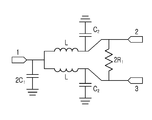
도 1은 종래 전력 분배 결합 회로를 예시한 도면이다.1 is a diagram illustrating a conventional power distribution coupling circuit.
도 1에 예시한 것과 같이 종래 전력 분배 결합 회로는 윌킨슨 전력 분배기/결합기보다 좁은 면적을 구현하기 위해서 커패시터와 인덕터를 이용하여 구현하였다. 하지만 여전히 큰 인덕터(L)로 인해 삽입 손실 증가와 넓은 칩 면적을 사용하여야 했다. 이와 같이 종래 송신기, 수신기, 증폭기, 위상배열 등 RF 회로에서 전력의 분배와 결합을 함에 있어 큰 인덕터 또는 긴 전송선로를 사용하고 있어 손실 증가와 회로의 면적 증가 등의 특성을 보완할 필요가 있다.As illustrated in FIG. 1, the conventional power distribution coupling circuit is implemented using a capacitor and an inductor to implement a smaller area than the Wilkinson power divider/combiner. However, due to the large inductor (L), it was necessary to increase the insertion loss and use a large chip area. As described above, in the distribution and coupling of power in RF circuits such as transmitters, receivers, amplifiers, and phased arrays, a large inductor or a long transmission line is used, so it is necessary to supplement characteristics such as increased loss and increased circuit area.
따라서 본 발명이 해결하고자 하는 기술적 과제는 저손실 소형 특성을 가지는 밀리미터파 전력 분배 결합 장치를 제공하는 것이다.Therefore, a technical problem to be solved by the present invention is to provide a millimeter wave power distribution coupling device having low loss and small size characteristics.
이러한 기술적 과제를 해결하기 위한 본 발명에 따른 전력 분배 결합 회로는 일단은 제1 포트에 연결되고, 타단은 제2 포트에 연결되는 제1 유도 소자, 일단은 상기 제1 포트와 상기 제1 유도 소자의 일단에 연결되고, 타단은 제3 포트에 연결되며, 상기 제1 유도 소자와 자기적으로(magnetically) 상호 결합되는 제2 유도 소자, 그리고 상기 제2 포트와 상기 제3 포트 사이에 연결되는 제1 커패시터를 포함한다.The power distribution coupling circuit according to the present invention for solving this technical problem is a first induction element, which is connected to a first port at one end and connected to a second port at the other end, and the first port and the first induction element at one end. Is connected to one end, the other end is connected to the third port, a second induction element magnetically (magnetically) mutually coupled to the first induction element, and the second port is connected between the third port Includes 1 capacitor.
상기 회로는 상기 제1 커패시터와 병렬로 상기 제2 포트와 상기 제3 포트 사이에 연결되는 저항을 더 포함할 수 있다.The circuit may further include a resistor connected between the second port and the third port in parallel with the first capacitor.
상기 회로는 일단이 상기 제1 포트에 연결되고 타단은 접지에 연결되는 제2 커패시터를 더 포함할 수 있다.The circuit may further include a second capacitor having one end connected to the first port and the other end connected to ground.
상기 회로는 일단이 상기 제2 포트와 상기 제1 유도 소자의 타단에 연결되고, 타단은 접지에 연결되는 제3 커패시터, 그리고 일단이 상기 제3 포트와 상기 제2 유도 소자의 타단에 연결되고, 타단은 접지에 연결되는 제4 커패시터를 더 포함할 수 있다.The circuit has one end connected to the second port and the other end of the first inductive element, the other end connected to a third capacitor connected to ground, and one end connected to the third port and the other end of the second inductive element, The other end may further include a fourth capacitor connected to ground.
상기 제1 유도 소자의 일단으로 유입되는 전류가 증가하면, 상기 제2 유도 소자의 일단에 유도기전력의 양의 극이 나타나도록 상기 제1 유도 소자와 상기 제2 유도 소자가 자기적으로 상호 결합될 수 있다.When the current flowing into one end of the first induction element increases, the first induction element and the second induction element are magnetically coupled to each other so that a positive pole of the induced electromotive force appears at one end of the second induction element. Can be.
상기 제1 유도 소자와 상기 제2 유도 소자는 인덕터 또는 트랜스미션 라인 중 어느 하나일 수 있다.The first inductive element and the second inductive element may be either an inductor or a transmission line.
본 발명에 의하면 저손실 소형 특성을 가지는 밀리미터파 전력 분배 결합 장치를 제공할 수 있다.According to the present invention, it is possible to provide a millimeter wave power distribution coupling device having low loss and small size characteristics.
도 1은 종래 전력 분배 결합 회로를 예시한 도면이다.
도 2는 본 발명의 일 실시예에 따른 전력 분배 결합 회로를 예시한 도면이다.
도 3은 도 2에 예시한 본 발명에 따른 전력 분배 결합 회로의 구성을 간소화한 등가 회로이다.
도 4는 도 2에 예시한 본 발명에 따른 전력 분배 결합 회로의 반회로 우모드 등가 회로이다.
도 5는 도 2에 예시한 본 발명에 따른 전력 분배 결합 회로의 반회로 기모드 등가 회로이다.
도 6은 도 1의 종래 회로의 격리도 특성을 위한 회로도이다.
도 7은 도 2에 예시한 본 발명에 따른 전력 분배 결합 회로의 격리도 특성을 위한 회로도이다.
도 8은 종래 기술과 본 발명에 따른 회로의 삽입 손실에 대한 이상적인 특성을 나타낸 그래프이다.
도 9는 종래 기술과 본 발명에 따른 회로의 반사 손실에 대한 이상적인 특성을 나타낸 그래프이다.
도 10은 종래 기술과 본 발명에 따른 회로의 격리도에 대한 이상적인 특성을 나타낸 그래프이다.
도 11은 본 발명에 따른 회로 실시예에 따른 제작 회로와 레이아웃을 나타낸 도면이다.
도 12는 본 발명에 따른 회로 실시예의 삽입 손실을 나타낸 그래프이다.
도 13은 본 발명에 따른 회로 실시예의 반사 손실을 나타낸 그래프이다.
도 14는 본 발명에 따른 회로 실시예의 격리도를 나타낸 그래프이다.
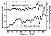
도 15는 본 발명에 따른 회로 실시예의 삽입 손실 크기와 위상 차이를 나타낸 그래프이다.1 is a diagram illustrating a conventional power distribution coupling circuit.
2 is a diagram illustrating a power distribution coupling circuit according to an embodiment of the present invention.
3 is an equivalent circuit that simplifies the configuration of the power distribution coupling circuit according to the present invention illustrated in FIG. 2.
4 is a half circuit right mode equivalent circuit of the power distribution coupling circuit according to the present invention illustrated in FIG. 2.
FIG. 5 is a half circuit group mode equivalent circuit of the power distribution coupling circuit according to the present invention illustrated in FIG. 2.
6 is a circuit diagram for isolation characteristics of the conventional circuit of FIG. 1.
7 is a circuit diagram for isolation characteristics of the power distribution coupling circuit according to the present invention illustrated in FIG. 2.
8 is a graph showing ideal characteristics for insertion loss of a circuit according to the prior art and the present invention.
9 is a graph showing ideal characteristics for return loss of a circuit according to the prior art and the present invention.
10 is a graph showing ideal characteristics for the isolation of the circuit according to the prior art and the present invention.
11 is a view showing a manufacturing circuit and a layout according to a circuit embodiment according to the present invention.
12 is a graph showing insertion loss of a circuit embodiment according to the present invention.
13 is a graph showing return loss of a circuit embodiment according to the present invention.
14 is a graph showing the isolation of the circuit embodiment according to the present invention.
15 is a graph showing the insertion loss magnitude and phase difference of the circuit embodiment according to the present invention.
이하 첨부된 도면을 참조하여 본 발명이 속하는 기술 분야에서 통상의 지식을 가진 자가 본 발명을 용이하게 실시할 수 있는 바람직한 실시 예를 상세히 설명한다. 그러나 이들 실시 예는 본 발명을 보다 구체적으로 설명하기 위한 것으로, 본 발명의 범위가 이에 의하여 제한되지 않는다는 것은 당업계의 통상의 지식을 가진 자에게 자명할 것이다.Hereinafter, preferred embodiments in which a person having ordinary knowledge in the art to which the present invention pertains can easily implement the present invention will be described in detail with reference to the accompanying drawings. However, these examples are intended to illustrate the present invention in more detail, and it will be apparent to those skilled in the art that the scope of the present invention is not limited thereby.
본 발명이 해결하고자 하는 과제의 해결 방안을 명확하게 하기 위한 발명의 구성을 본 발명의 바람직한 실시 예에 근거하여 첨부 도면을 참조하여 상세히 설명하되, 도면의 구성요소들에 참조번호를 부여함에 있어서 동일 구성요소에 대해서는 비록 다른 도면상에 있더라도 동일 참조번호를 부여하였으며 당해 도면에 대한 설명시 필요한 경우 다른 도면의 구성요소를 인용할 수 있음을 미리 밝혀둔다. 아울러 본 발명의 바람직한 실시 예에 대한 동작 원리를 상세하게 설명함에 있어 본 발명과 관련된 공지 기능 혹은 구성에 대한 구체적인 설명 그리고 그이외의 제반 사항이 본 발명의 요지를 불필요하게 흐릴 수 있다고 판단되는 경우, 그 상세한 설명을 생략한다.The configuration of the invention for clarifying the solution to the problem to be solved by the present invention will be described in detail with reference to the accompanying drawings based on preferred embodiments of the present invention, but the same is used in assigning reference numbers to components of the drawings. The same reference numerals are assigned to the components even though they are on other drawings, and it is revealed in advance that components of other drawings may be cited when necessary for the description of the drawings. In addition, in the detailed description of the operating principle of the preferred embodiment of the present invention, if it is determined that a detailed description of known functions or configurations related to the present invention and other matters may unnecessarily obscure the subject matter of the present invention, The detailed description is omitted.
덧붙여, 명세서 전체에서, 어떤 부분이 다른 부분과 '연결'되어 있다고 할때, 이는 '직접적으로 연결'되어 있는 경우뿐만 아니라, 그 중간에 다른 소자를 사이에 두고 '간접적으로 연결'되어 있는 경우도 포함한다. 본 명세서에서, 단수형은 문구에서 특별히 언급하지 않는 한 복수형도 포함한다. 명세서에서 사용되는 "포함한다(comprises)" 또는 "포함하는(comprising)"은 언급된 구성요소, 단계, 동작, 또는 소자 외에 하나 이상의 다른 구성요소, 단계, 동작, 또는 소자의 존재 또는 추가를 배제하지 않는다.In addition, in the specification, when a part is said to be'connected' to another part, it is not only'directly connected', but also'indirectly connected' with another element in between. Includes. In the present specification, the singular form also includes the plural form unless otherwise specified in the phrase. As used herein, "comprises" or "comprising" excludes the presence or addition of one or more other components, steps, operations, or elements other than the components, steps, operations, or elements mentioned. I never do that.
본 명세서에서 유도 소자는 인덕터로 설명하나, 인덕턴스를 가지는 소자로 트랜스미션 라인, 인덕터 등이 포함될 수 있다.The induction element is described as an inductor in this specification, but may include a transmission line, an inductor, etc. as an element having an inductance.
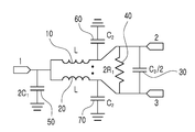
도 2는 본 발명의 일 실시예에 따른 전력 분배 결합 회로를 예시한 도면이다.2 is a diagram illustrating a power distribution coupling circuit according to an embodiment of the present invention.
도 2를 참고하면, 본 발명에 따른 전력 분배 결합 회로는 제1 인덕터(10)와 제2 인덕터(20), 제1 커패시터(30), 저항(40), 제2 커패시터(50), 제3 커패시터(60) 및 제4 커패시터(70)를 포함할 수 있다.Referring to FIG. 2, the power distribution coupling circuit according to the present invention includes a
제1 인덕터(10)와 제2 인덕터(20)는 자기적으로(magnetically) 상호 결합된 한 쌍의 결합 인덕터로 구현될 수 있다.The
제1 인덕터(10)는 일단은 제1 포트(1)에 연결되고, 타단은 제2 포트(2)에 연결될 수 있다.The
제2 인덕터(20)는 일단은 제1 포트(1)에 연결되고, 타단은 제3 포트(3)에 연결될 수 있다.The
제1 인덕터(10)와 제2 인덕터(20)는 자기적으로(magnetically) 상호 결합될 수 있다.The
제1 인덕터(10)와 제2 인덕터(20)는 간단히 구현하기 위하여 일반적으로 전송 라인과 저항으로 구현될 수 있으며, 대칭적인 구조를 가질 수 있다. 실제 인덕터 전자 소자를 사용하지 않고 전송 라인의 길이를 조절하는 방식으로 상기 인덕터가 구현될 수도 있다. 이때, 상기 전송 라인의 길이는 λ/4가 된다. 여기서, λ는 파장이다. 제1 인덕터(10)의 일단으로 유입되는 전류가 증가하면, 제2 인덕터(20)의 일단에 유도기전력의 양의 극이 나타나도록 제1 인덕터(10)와 제2 인덕터(20)는 자기적으로 상호 결합되게 배치될 수 있다.The
제1 커패시터(30)는 제2 포트(2)와 제3 포트(3) 사이에 연결될 수 있다.The
저항(40)은 제1 커패시터(30)와 병렬로 제2 포트(2)와 제3 포트(3) 사이에 연결될 수 있다.The
제2 커패시터(50)는 일단이 제1 포트(1)에 연결되고 타단은 접지에 연결될 수 있다.The
제3 커패시터(60)는 일단이 제2 포트(2)에 연결되고 타단은 접지에 연결될 수 있다.The
제4 커패시터(70)는 일단이 제3 포트(3)에 연결되고 타단은 접지에 연결될 수 있다.The
도 1에 나타낸 종래 전력 분배 결합 회로와 비교하기 위해서, 도 2의 전력 분배 결합 회로에서 제1 인덕터(10)와 제2 인덕터(20)의 인덕턴스는 'L'로 동일하고, 상호 인덕턴스는 'M'이라고 가정한다. 그리고 제1 커패시터(30)의 커패시턴스는 'C3/2', 제2 커패시터(50)의 커패시턴스는 '2C1', 제3 커패시터(60)와 제4 커패시터(70)의 커패시턴스는 'C2', 저항(40)의 저항은 '2R1'으로 가정한다.For comparison with the conventional power distribution coupling circuit shown in FIG. 1, in the power distribution coupling circuit of FIG. 2, the inductances of the
즉 본 발명에 따른 전력 분배 결합 회로는 도 1에서 예시한 종래 회로에 비해 자기적으로 상호 결합된 한 쌍의 결합 인덕터(10, 20)와 션트(shunt) 커패시터(30)를 포함하는 점에서 차이가 있다.That is, the power distribution coupling circuit according to the present invention differs in that it includes a pair of
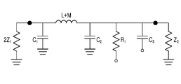
도 3은 도 2에 예시한 본 발명에 따른 전력 분배 결합 회로의 구성을 간소화한 등가 회로이다.3 is an equivalent circuit that simplifies the configuration of the power distribution coupling circuit according to the present invention illustrated in FIG. 2.
도 2에 나타낸 본 발명에 따른 전력 분배 결합 회로에 대해서 우모드/기모드(even/odd) 해석법을 이용하여 해석한다. even/odd 해석법은 커플링이 일어나는 선로에 대한 회로 해석법 중 하나이다. 예를 들어, 두 선로에 교류 전류가 흐르는 경우, 두 선로에 흐르는 교류 전류의 방향이 같은지 또는 다른지를 알 수가 없다. 따라서, 먼저 두 선로에 흐르는 교류 전류의 방향을 동일하다고 가정하여 수학적으로 회로를 해석하는 것이 우모드 해석 방법이고, 상기 두 선로에 흐르는 교류 전류의 방향을 다르다고 가정하여 수학적으로 회로를 해석하는 것이 기모드 해석 방법이다.The power distribution coupling circuit according to the present invention shown in Fig. 2 is analyzed using a right mode/even mode analysis method. The even/odd analysis is one of the circuit analysis methods for the line where coupling occurs. For example, when an alternating current flows through two lines, it is impossible to know whether the directions of alternating currents flowing through the two lines are the same or different. Therefore, first, it is a right mode analysis method to mathematically analyze a circuit by assuming that the directions of alternating currents flowing in two lines are the same. It is a mode analysis method.
도 4는 도 2에 예시한 본 발명에 따른 전력 분배 결합 회로의 반회로 우모드 등가 회로이고, 도 5는 도 2에 예시한 본 발명에 따른 전력 분배 결합 회로의 반회로 기모드 등가 회로이다.FIG. 4 is a half circuit right mode equivalent circuit of the power distribution coupling circuit according to the present invention illustrated in FIG. 2, and FIG. 5 is a half circuit group mode equivalent circuit of the power distribution coupling circuit according to the present invention illustrated in FIG. 2.
도 2에 예시한 본 발명에 따른 전력 분배 결합 회로는 도 4에 예시한 우모드에서 보는 것처럼, 인덕턴스를 L+M으로 향상시켜 도 1에 예시한 종래 기술보다 작은 인덕턴스로 같은 성능을 가진다. 작은 인덕턴스는 기생 저항성분을 작게 줄여 삽입 손실을 감소시키고, 인덕터와 같은 유도소자의 크기를 감소하여 칩 면적을 줄인다. 이때 포트 1(1)과 포트 2(2)의 입력 임피던스(Z1, Z2)는 아래 수학식 1과 같은 값을 가지며, 도 1에 예시한 종래 기술에 따른 회로와 같은 결과를 가진다. 그리고 인덕턴스와 커패시턴스의 값은 아래 수학식 2와 같다.The power distribution coupling circuit according to the present invention illustrated in FIG. 2 has the same performance with a smaller inductance than the prior art illustrated in FIG. 1 by improving the inductance to L+M, as seen in the right mode illustrated in FIG. 4. The small inductance reduces the parasitic resistance component to reduce the insertion loss and the size of the inductor, such as an inductor, to reduce the chip area. At this time, the input impedances Z 1 and Z 2 of the port 1(1) and the port 2(2) have the same values as in
[수학식 1][Equation 1]

[수학식 2][Equation 2]

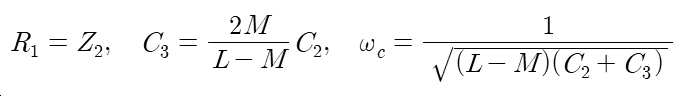
도 2에 예시한 본 발명에 따른 전력 분배 결합 회로는 도 5에 예시한 기모드에서는 인덕턴스 값이 L-M으로 감소하여, C3 커패시터를 추가하게 된다. 추가된 커패시터는 포트 2(2)와 포트 3(3)이 매칭되도록 하며, 그 임피던스는 아래 수학식 3과 같다.The power distribution coupling circuit according to the present invention illustrated in FIG. 2 reduces the inductance value to LM in the group mode illustrated in FIG. 5 to add a C 3 capacitor. The added capacitor causes port 2(2) and port 3(3) to match, and the impedance is as shown in
[수학식 3][Equation 3]

이때 저항 값(R1), 캐패시턴스(C3) 및 중심주파수(ωc)는 아래 수학식 4와 같다.At this time, the resistance value R1, the capacitance C 3 , and the center frequency ω c are as shown in Equation 4 below.
[수학식 4][Equation 4]
도 6은 도 1의 종래 회로의 격리도 특성을 위한 회로도이고, 도 7은 도 2에 예시한 본 발명에 따른 전력 분배 결합 회로의 격리도 특성을 위한 회로도이다.6 is a circuit diagram for isolation characteristics of the conventional circuit of FIG. 1, and FIG. 7 is a circuit diagram for isolation characteristics of the power distribution coupling circuit according to the present invention illustrated in FIG.
도 6 및 도 7을 참고하면, 종래 기술에 따른 도 1의 회로에서 격리도 특성(Y32,CLC)은 수학식 5와 같고, 본 발명에 따른 도 2의 회로에서 격리도 특성(Y32,coupledL)은 수학식 6과 같다.6 and 7, in the circuit of FIG. 1 according to the prior art, the isolation characteristics (Y 32, CLC ) are the same as in Equation 5, and in the circuit of FIG. 2 according to the present invention, the isolation characteristics (Y 32, coupledL ) is as shown in Equation 6.
[수학식 5][Equation 5]
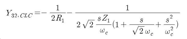
[수학식 6][Equation 6]

종래 회로 및 본 발명에 따른 장치 모두 격리도 값은 중심주파수에서 모두가 큰 값을 가진다. The isolation value of both the conventional circuit and the device according to the present invention has a large value at the center frequency.
도 8은 종래 기술과 본 발명에 따른 회로의 삽입 손실에 대한 이상적인 특성을 나타낸 그래프이고, 도 9는 종래 기술과 본 발명에 따른 회로의 반사 손실에 대한 이상적인 특성을 나타낸 그래프이며, 도 10은 종래 기술과 본 발명에 따른 회로의 격리도에 대한 이상적인 특성을 나타낸 그래프이다.8 is a graph showing ideal characteristics for insertion loss of a circuit according to the prior art and the present invention, FIG. 9 is a graph showing ideal characteristics for return loss of a circuit according to the prior art and the present invention, and FIG. 10 is a conventional graph It is a graph showing the ideal characteristics for the isolation of the circuit according to the technology and the invention.
도 8 내지 도 10에서 확인할 수 있는 것과 같이, 손실을 가지지 않는 이상적인 경우, 종래 기술에 따른 도 1의 장치와 본 발명에 따른 도 2의 장치에서 입력 손실, 반사 손실 및 격리도는 모두 같은 값을 가진다.As can be seen in FIGS. 8 to 10, in the ideal case of no loss, the input loss, return loss, and isolation in the device of FIG. 1 according to the prior art and the device of FIG. 2 according to the present invention all have the same value. .
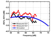
도 11은 본 발명에 따른 회로 실시예에 따른 제작 회로와 레이아웃을 나타낸 도면이고, 도 12는 본 발명에 따른 회로 실시예의 삽입 손실을 나타낸 그래프이고, 도 13은 본 발명에 따른 회로 실시예의 반사 손실을 나타낸 그래프이며, 도 14는 본 발명에 따른 회로 실시예의 격리도를 나타낸 그래프이고, 도 15는 본 발명에 따른 회로 실시예의 삽입 손실 크기와 위상 차이를 나타낸 그래프이다.11 is a view showing a manufacturing circuit and a layout according to a circuit embodiment according to the present invention, FIG. 12 is a graph showing insertion loss of a circuit embodiment according to the present invention, and FIG. 13 is a return loss of the circuit embodiment according to the present invention 14 is a graph showing the isolation of the circuit embodiment according to the present invention, and FIG. 15 is a graph showing the insertion loss magnitude and phase difference of the circuit embodiment according to the present invention.
도 11에 예시한 것과 같이 본 발명에 따른 전력 분배 결합 장치를 제작하여 삽입 손실, 반사 손실 및 격리도 등을 측정한 결과 낮은 삽입 손실 특성을 가지고, 반사 손실과 격리도 특성은 유사한 값을 가지는 것을 확인하였다.As illustrated in FIG. 11, a power distribution coupling device according to the present invention is manufactured to measure insertion loss, reflection loss, and isolation, and as a result, has low insertion loss characteristics, and reflection loss and isolation characteristics have similar values. Confirmed.
도 2에 예시한 본 발명에 따른 회로는 종래보다 더 작은 인덕턴스를 가지면서 윌킨스 전력 분배기/결합기의 고유한 특성을 구현가능하고, 인덕터 사이를 가깝게 구현하여 종래 기술보다 삽입 손실 성능을 향상시키는 동시에 50% 이상의 사용 면적 감소가 가능하다.The circuit according to the present invention illustrated in FIG. 2 is capable of realizing the unique characteristics of a Wilkins power divider/combiner while having a smaller inductance than the prior art, and implementing close proximity between the inductors to improve insertion loss performance over the prior art, while at the
본 발명에 의한 저손실 소형 특성을 가지는 밀리미터파 전력 분배 결합 장치는 5G 이동통신뿐만 아니라, 이동통신과 무선랜을 포함하는 다양한 무선, 유선 통신 등의 회로에 활용 가능하다. 또한 RF 송신기와 수신기, 전력증폭기 등에서 전력 분배와 결합을 수행하는 부품으로 활용이 가능하다.The millimeter-wave power distribution combining device having a low-loss small size characteristic according to the present invention can be used not only for 5G mobile communication, but also for various wireless and wired circuits including mobile communication and wireless LAN. In addition, it can be used as a component that performs power distribution and coupling in RF transmitters, receivers, and power amplifiers.
이상에서 본 발명의 바람직한 실시예에 대하여 상세하게 설명하였지만 본 발명의 권리범위는 이에 한정되는 것은 아니고 다음의 청구범위에서 정의하고 있는 본 발명의 기본 개념을 이용한 당업자의 여러 변형 및 개량 형태 또한 본 발명의 권리범위에 속하는 것이다.Although the preferred embodiments of the present invention have been described in detail above, the scope of the present invention is not limited thereto, and various modifications and improvements of those skilled in the art using the basic concept of the present invention defined in the following claims are also provided. It belongs to the scope of rights.
Claims (6)
일단은 상기 제1 포트와 상기 제1 유도 소자의 일단에 연결되고, 타단은 제3 포트에 연결되며, 상기 제1 유도 소자와 자기적으로(magnetically) 상호 결합되는 제2 유도 소자, 그리고
상기 제2 포트와 상기 제3 포트 사이에 연결되는 제1 커패시터
를 포함하는 전력 분배 결합 회로.First induction element is connected to the first port, the other end is connected to the second port,
One end is connected to one end of the first port and the first induction element, the other end is connected to a third port, a second induction element magnetically coupled to the first induction element (magnetically), and
A first capacitor connected between the second port and the third port
Power distribution coupling circuit comprising a.
상기 제1 커패시터와 병렬로 상기 제2 포트와 상기 제3 포트 사이에 연결되는 저항
을 더 포함하는 전력 분배 결합 회로.In claim 1,
A resistor connected between the second port and the third port in parallel with the first capacitor
Power distribution coupling circuit further comprising a.
일단이 상기 제1 포트에 연결되고 타단은 접지에 연결되는 제2 커패시터
를 더 포함하는 전력 분배 결합 회로.In claim 1,
A second capacitor, one end of which is connected to the first port and the other end of which is connected to ground
Power distribution coupling circuit further comprising a.
일단이 상기 제2 포트와 상기 제1 유도 소자의 타단에 연결되고, 타단은 접지에 연결되는 제3 커패시터, 그리고
일단이 상기 제3 포트와 상기 제2 유도 소자의 타단에 연결되고, 타단은 접지에 연결되는 제4 커패시터
를 더 포함하는 전력 분배 결합 회로.In claim 1,
A third capacitor having one end connected to the second port and the other end of the first induction element, the other end connected to ground, and
A fourth capacitor having one end connected to the third port and the other end of the second inductive element, and the other end connected to ground.
Power distribution coupling circuit further comprising.
상기 제1 유도 소자의 일단으로 유입되는 전류가 증가하면, 상기 제2 유도 소자의 일단에 유도기전력의 양의 극이 나타나도록 상기 제1 유도 소자와 상기 제2 유도 소자가 자기적으로 상호 결합되어 있는 전력 분배 결합 회로.In claim 1,
When the current flowing into one end of the first induction element increases, the first induction element and the second induction element are magnetically coupled to each other so that a positive pole of the induced electromotive force appears at one end of the second induction element. Power distribution coupling circuit.
상기 제1 유도 소자와 상기 제2 유도 소자는 인덕터 또는 트랜스미션 라인 중 어느 하나인 전력 분배 결합 회로.In claim 1,
The first inductive element and the second inductive element are either an inductor or a transmission line, a power distribution coupling circuit.
Priority Applications (2)
| Application Number | Priority Date | Filing Date | Title |
|---|---|---|---|
| KR1020180154326A KR102200380B1 (en) | 2018-12-04 | 2018-12-04 | Compact low loss millimeter-wave power divider and combiner device |
| PCT/KR2019/002485 WO2020116715A1 (en) | 2018-12-04 | 2019-03-05 | Compact low-loss millimeter wave power dividing/combining apparatus |
Applications Claiming Priority (1)
| Application Number | Priority Date | Filing Date | Title |
|---|---|---|---|
| KR1020180154326A KR102200380B1 (en) | 2018-12-04 | 2018-12-04 | Compact low loss millimeter-wave power divider and combiner device |
Publications (2)
| Publication Number | Publication Date |
|---|---|
| KR20200067455A true KR20200067455A (en) | 2020-06-12 |
| KR102200380B1 KR102200380B1 (en) | 2021-01-07 |
Family
ID=70973731
Family Applications (1)
| Application Number | Title | Priority Date | Filing Date |
|---|---|---|---|
| KR1020180154326A KR102200380B1 (en) | 2018-12-04 | 2018-12-04 | Compact low loss millimeter-wave power divider and combiner device |
Country Status (2)
| Country | Link |
|---|---|
| KR (1) | KR102200380B1 (en) |
| WO (1) | WO2020116715A1 (en) |
Cited By (1)
| Publication number | Priority date | Publication date | Assignee | Title |
|---|---|---|---|---|
| KR20220001622A (en) * | 2020-06-30 | 2022-01-06 | 영남대학교 산학협력단 | Millimeter wave power and phase difference detector and image processing method using the same |
Families Citing this family (1)
| Publication number | Priority date | Publication date | Assignee | Title |
|---|---|---|---|---|
| TWI747460B (en) * | 2020-08-25 | 2021-11-21 | 國立暨南國際大學 | Power divider |
Citations (3)
| Publication number | Priority date | Publication date | Assignee | Title |
|---|---|---|---|---|
| KR20100004440A (en) * | 2008-07-03 | 2010-01-13 | 광운대학교 산학협력단 | Power divider and combiner using lumped elements |
| KR20170066915A (en) * | 2015-12-07 | 2017-06-15 | 삼성전자주식회사 | Power combinder/divider using mutual inductance |
| KR101761300B1 (en) * | 2016-05-12 | 2017-08-04 | 충남대학교산학협력단 | Low insertion loss, wideband, and compact power divider |
Family Cites Families (2)
| Publication number | Priority date | Publication date | Assignee | Title |
|---|---|---|---|---|
| KR100974620B1 (en) * | 2008-05-23 | 2010-08-06 | 경성대학교 산학협력단 | Tunable Wilkinson Power Divider Combiner |
| KR100897864B1 (en) * | 2008-12-15 | 2009-05-18 | 주식회사 이공 | Power divider using coupling |
-
2018
- 2018-12-04 KR KR1020180154326A patent/KR102200380B1/en active IP Right Grant
-
2019
- 2019-03-05 WO PCT/KR2019/002485 patent/WO2020116715A1/en active Application Filing
Patent Citations (3)
| Publication number | Priority date | Publication date | Assignee | Title |
|---|---|---|---|---|
| KR20100004440A (en) * | 2008-07-03 | 2010-01-13 | 광운대학교 산학협력단 | Power divider and combiner using lumped elements |
| KR20170066915A (en) * | 2015-12-07 | 2017-06-15 | 삼성전자주식회사 | Power combinder/divider using mutual inductance |
| KR101761300B1 (en) * | 2016-05-12 | 2017-08-04 | 충남대학교산학협력단 | Low insertion loss, wideband, and compact power divider |
Cited By (1)
| Publication number | Priority date | Publication date | Assignee | Title |
|---|---|---|---|---|
| KR20220001622A (en) * | 2020-06-30 | 2022-01-06 | 영남대학교 산학협력단 | Millimeter wave power and phase difference detector and image processing method using the same |
Also Published As
| Publication number | Publication date |
|---|---|
| WO2020116715A1 (en) | 2020-06-11 |
| KR102200380B1 (en) | 2021-01-07 |
Similar Documents
| Publication | Publication Date | Title |
|---|---|---|
| KR102589737B1 (en) | Power combinder/divider using mutual inductance | |
| RU2143160C1 (en) | Balancer, radio communication device, and antenna assembly designing process | |
| US20100244981A1 (en) | Radio frequency power divider and combiner circuit | |
| US10516379B2 (en) | Coupled resonator on-die filters for WiFi applications | |
| TW201304401A (en) | Transceiver and integrated circuit | |
| US20070075802A1 (en) | Wide-bandwidth balanced transformer | |
| EP2920841B1 (en) | Compact power divider/combiner with flexible output spacing | |
| US8598964B2 (en) | Balun with intermediate non-terminated conductor | |
| CN106785251A (en) | Mode transmission ultra-broadband digital phase shifter | |
| CN109560360A (en) | A kind of directional coupler | |
| CN104241749B (en) | A kind of controllable microstrip filter of transmission zero | |
| KR102200380B1 (en) | Compact low loss millimeter-wave power divider and combiner device | |
| CN109888441A (en) | The adjustable balanced type model filters power splitter of bandwidth | |
| CN107293835A (en) | Single-unit Wilkinson power divider | |
| US11699056B2 (en) | RFID inlay | |
| JP2007019696A (en) | High-frequency switching circuit, radio equipment, and signal path switching unit | |
| KR102591621B1 (en) | Microwave power combiner | |
| CN108110388A (en) | Electricity adjusts the constant bandwidth broadband filter of transmission zero | |
| US10438732B2 (en) | Monolithic wideband trifilar transformer | |
| CN101951232A (en) | Radio-frequency (RF) power amplifier | |
| Taravati et al. | An efficient method of designing dual‐and wide‐band power dividers with arbitrary power division | |
| US11011818B1 (en) | Transformer having series and parallel connected transmission lines | |
| CN111987416B (en) | Terminal equipment | |
| WO2014159172A1 (en) | Passive radio frequency signal handler | |
| US11043931B2 (en) | Power combiner/divider |
Legal Events
| Date | Code | Title | Description |
|---|---|---|---|
| E90F | Notification of reason for final refusal | ||
| E701 | Decision to grant or registration of patent right | ||
| GRNT | Written decision to grant |