KR20200063102A - Filming assembly and its packaging method, lens module, electronic device - Google Patents
Filming assembly and its packaging method, lens module, electronic device Download PDFInfo
- Publication number
- KR20200063102A KR20200063102A KR1020197036797A KR20197036797A KR20200063102A KR 20200063102 A KR20200063102 A KR 20200063102A KR 1020197036797 A KR1020197036797 A KR 1020197036797A KR 20197036797 A KR20197036797 A KR 20197036797A KR 20200063102 A KR20200063102 A KR 20200063102A
- Authority
- KR
- South Korea
- Prior art keywords
- forming
- packaging
- layer
- conductive
- filter
- Prior art date
Links
- 238000004806 packaging method and process Methods 0.000 title claims abstract description 150
- 238000000034 method Methods 0.000 title claims abstract description 135
- 238000003466 welding Methods 0.000 claims abstract description 98
- 239000000758 substrate Substances 0.000 claims abstract description 83
- 238000003384 imaging method Methods 0.000 claims abstract description 42
- 230000008569 process Effects 0.000 claims description 90
- 230000002093 peripheral effect Effects 0.000 claims description 49
- 229910052751 metal Inorganic materials 0.000 claims description 17
- 239000002184 metal Substances 0.000 claims description 17
- 238000000059 patterning Methods 0.000 claims description 7
- 239000005022 packaging material Substances 0.000 claims description 6
- 238000009713 electroplating Methods 0.000 claims description 5
- 238000000227 grinding Methods 0.000 claims description 4
- 238000010329 laser etching Methods 0.000 claims description 4
- 239000000853 adhesive Substances 0.000 description 36
- 230000001070 adhesive effect Effects 0.000 description 35
- 239000000463 material Substances 0.000 description 30
- 230000003287 optical effect Effects 0.000 description 22
- 230000035882 stress Effects 0.000 description 19
- 239000011521 glass Substances 0.000 description 18
- 238000000576 coating method Methods 0.000 description 10
- 238000010586 diagram Methods 0.000 description 10
- 239000011248 coating agent Substances 0.000 description 9
- 239000006260 foam Substances 0.000 description 9
- 238000004519 manufacturing process Methods 0.000 description 9
- 239000000243 solution Substances 0.000 description 8
- 230000005540 biological transmission Effects 0.000 description 7
- 238000003860 storage Methods 0.000 description 7
- 230000010354 integration Effects 0.000 description 6
- 230000009471 action Effects 0.000 description 5
- 239000003822 epoxy resin Substances 0.000 description 5
- 238000005530 etching Methods 0.000 description 5
- 238000012858 packaging process Methods 0.000 description 5
- 229920000647 polyepoxide Polymers 0.000 description 5
- 238000004904 shortening Methods 0.000 description 5
- 239000004593 Epoxy Substances 0.000 description 4
- XUIMIQQOPSSXEZ-UHFFFAOYSA-N Silicon Chemical compound [Si] XUIMIQQOPSSXEZ-UHFFFAOYSA-N 0.000 description 4
- UMIVXZPTRXBADB-UHFFFAOYSA-N benzocyclobutene Chemical compound C1=CC=C2CCC2=C1 UMIVXZPTRXBADB-UHFFFAOYSA-N 0.000 description 4
- 230000015572 biosynthetic process Effects 0.000 description 4
- 238000009792 diffusion process Methods 0.000 description 4
- 230000000694 effects Effects 0.000 description 4
- 229920002577 polybenzoxazole Polymers 0.000 description 4
- 238000007789 sealing Methods 0.000 description 4
- 239000004065 semiconductor Substances 0.000 description 4
- 230000008054 signal transmission Effects 0.000 description 4
- 229910052710 silicon Inorganic materials 0.000 description 4
- 239000010703 silicon Substances 0.000 description 4
- RYGMFSIKBFXOCR-UHFFFAOYSA-N Copper Chemical compound [Cu] RYGMFSIKBFXOCR-UHFFFAOYSA-N 0.000 description 3
- 239000004642 Polyimide Substances 0.000 description 3
- 239000004020 conductor Substances 0.000 description 3
- 229910052802 copper Inorganic materials 0.000 description 3
- 239000010949 copper Substances 0.000 description 3
- 238000001746 injection moulding Methods 0.000 description 3
- 238000002161 passivation Methods 0.000 description 3
- 229920001721 polyimide Polymers 0.000 description 3
- 238000000992 sputter etching Methods 0.000 description 3
- ATJFFYVFTNAWJD-UHFFFAOYSA-N Tin Chemical compound [Sn] ATJFFYVFTNAWJD-UHFFFAOYSA-N 0.000 description 2
- 230000002411 adverse Effects 0.000 description 2
- 230000000903 blocking effect Effects 0.000 description 2
- 230000009172 bursting Effects 0.000 description 2
- 230000007797 corrosion Effects 0.000 description 2
- 238000005260 corrosion Methods 0.000 description 2
- 239000013078 crystal Substances 0.000 description 2
- 238000005516 engineering process Methods 0.000 description 2
- PCHJSUWPFVWCPO-UHFFFAOYSA-N gold Chemical compound [Au] PCHJSUWPFVWCPO-UHFFFAOYSA-N 0.000 description 2
- 239000010931 gold Substances 0.000 description 2
- 229910052737 gold Inorganic materials 0.000 description 2
- 230000001590 oxidative effect Effects 0.000 description 2
- 238000000206 photolithography Methods 0.000 description 2
- 230000005855 radiation Effects 0.000 description 2
- XLYOFNOQVPJJNP-UHFFFAOYSA-N water Chemical compound O XLYOFNOQVPJJNP-UHFFFAOYSA-N 0.000 description 2
- 229910052581 Si3N4 Inorganic materials 0.000 description 1
- VYPSYNLAJGMNEJ-UHFFFAOYSA-N Silicium dioxide Chemical compound O=[Si]=O VYPSYNLAJGMNEJ-UHFFFAOYSA-N 0.000 description 1
- 229910052782 aluminium Inorganic materials 0.000 description 1
- XAGFODPZIPBFFR-UHFFFAOYSA-N aluminium Chemical compound [Al] XAGFODPZIPBFFR-UHFFFAOYSA-N 0.000 description 1
- 238000004458 analytical method Methods 0.000 description 1
- 230000000712 assembly Effects 0.000 description 1
- 238000000429 assembly Methods 0.000 description 1
- 239000003990 capacitor Substances 0.000 description 1
- 230000006835 compression Effects 0.000 description 1
- 238000007906 compression Methods 0.000 description 1
- 230000006866 deterioration Effects 0.000 description 1
- 230000002542 deteriorative effect Effects 0.000 description 1
- 230000005684 electric field Effects 0.000 description 1
- 238000011049 filling Methods 0.000 description 1
- 238000010438 heat treatment Methods 0.000 description 1
- 230000006872 improvement Effects 0.000 description 1
- 238000003698 laser cutting Methods 0.000 description 1
- 238000012986 modification Methods 0.000 description 1
- 230000004048 modification Effects 0.000 description 1
- 239000012778 molding material Substances 0.000 description 1
- 238000000465 moulding Methods 0.000 description 1
- 239000004033 plastic Substances 0.000 description 1
- 229920003023 plastic Polymers 0.000 description 1
- 150000003071 polychlorinated biphenyls Chemical class 0.000 description 1
- 238000003825 pressing Methods 0.000 description 1
- 230000006798 recombination Effects 0.000 description 1
- 238000005215 recombination Methods 0.000 description 1
- HQVNEWCFYHHQES-UHFFFAOYSA-N silicon nitride Chemical compound N12[Si]34N5[Si]62N3[Si]51N64 HQVNEWCFYHHQES-UHFFFAOYSA-N 0.000 description 1
- 229910052814 silicon oxide Inorganic materials 0.000 description 1
- 238000001179 sorption measurement Methods 0.000 description 1
- 230000008093 supporting effect Effects 0.000 description 1
- 230000008646 thermal stress Effects 0.000 description 1
- WFKWXMTUELFFGS-UHFFFAOYSA-N tungsten Chemical compound [W] WFKWXMTUELFFGS-UHFFFAOYSA-N 0.000 description 1
- 229910052721 tungsten Inorganic materials 0.000 description 1
- 239000010937 tungsten Substances 0.000 description 1
Images


Classifications
-
- H04N5/2254—
-
- G—PHYSICS
- G02—OPTICS
- G02B—OPTICAL ELEMENTS, SYSTEMS OR APPARATUS
- G02B5/00—Optical elements other than lenses
- G02B5/20—Filters
-
- G—PHYSICS
- G02—OPTICS
- G02B—OPTICAL ELEMENTS, SYSTEMS OR APPARATUS
- G02B7/00—Mountings, adjusting means, or light-tight connections, for optical elements
- G02B7/02—Mountings, adjusting means, or light-tight connections, for optical elements for lenses
-
- G—PHYSICS
- G02—OPTICS
- G02B—OPTICAL ELEMENTS, SYSTEMS OR APPARATUS
- G02B7/00—Mountings, adjusting means, or light-tight connections, for optical elements
- G02B7/02—Mountings, adjusting means, or light-tight connections, for optical elements for lenses
- G02B7/021—Mountings, adjusting means, or light-tight connections, for optical elements for lenses for more than one lens
-
- H—ELECTRICITY
- H01—ELECTRIC ELEMENTS
- H01L—SEMICONDUCTOR DEVICES NOT COVERED BY CLASS H10
- H01L27/00—Devices consisting of a plurality of semiconductor or other solid-state components formed in or on a common substrate
- H01L27/14—Devices consisting of a plurality of semiconductor or other solid-state components formed in or on a common substrate including semiconductor components sensitive to infrared radiation, light, electromagnetic radiation of shorter wavelength or corpuscular radiation and specially adapted either for the conversion of the energy of such radiation into electrical energy or for the control of electrical energy by such radiation
- H01L27/144—Devices controlled by radiation
- H01L27/146—Imager structures
- H01L27/14601—Structural or functional details thereof
- H01L27/14618—Containers
-
- H—ELECTRICITY
- H01—ELECTRIC ELEMENTS
- H01L—SEMICONDUCTOR DEVICES NOT COVERED BY CLASS H10
- H01L27/00—Devices consisting of a plurality of semiconductor or other solid-state components formed in or on a common substrate
- H01L27/14—Devices consisting of a plurality of semiconductor or other solid-state components formed in or on a common substrate including semiconductor components sensitive to infrared radiation, light, electromagnetic radiation of shorter wavelength or corpuscular radiation and specially adapted either for the conversion of the energy of such radiation into electrical energy or for the control of electrical energy by such radiation
- H01L27/144—Devices controlled by radiation
- H01L27/146—Imager structures
- H01L27/14601—Structural or functional details thereof
- H01L27/14636—Interconnect structures
-
- H—ELECTRICITY
- H01—ELECTRIC ELEMENTS
- H01L—SEMICONDUCTOR DEVICES NOT COVERED BY CLASS H10
- H01L27/00—Devices consisting of a plurality of semiconductor or other solid-state components formed in or on a common substrate
- H01L27/14—Devices consisting of a plurality of semiconductor or other solid-state components formed in or on a common substrate including semiconductor components sensitive to infrared radiation, light, electromagnetic radiation of shorter wavelength or corpuscular radiation and specially adapted either for the conversion of the energy of such radiation into electrical energy or for the control of electrical energy by such radiation
- H01L27/144—Devices controlled by radiation
- H01L27/146—Imager structures
- H01L27/14683—Processes or apparatus peculiar to the manufacture or treatment of these devices or parts thereof
-
- H—ELECTRICITY
- H04—ELECTRIC COMMUNICATION TECHNIQUE
- H04M—TELEPHONIC COMMUNICATION
- H04M1/00—Substation equipment, e.g. for use by subscribers
- H04M1/02—Constructional features of telephone sets
-
- H—ELECTRICITY
- H04—ELECTRIC COMMUNICATION TECHNIQUE
- H04M—TELEPHONIC COMMUNICATION
- H04M1/00—Substation equipment, e.g. for use by subscribers
- H04M1/02—Constructional features of telephone sets
- H04M1/0202—Portable telephone sets, e.g. cordless phones, mobile phones or bar type handsets
- H04M1/026—Details of the structure or mounting of specific components
- H04M1/0264—Details of the structure or mounting of specific components for a camera module assembly
-
- H—ELECTRICITY
- H04—ELECTRIC COMMUNICATION TECHNIQUE
- H04N—PICTORIAL COMMUNICATION, e.g. TELEVISION
- H04N23/00—Cameras or camera modules comprising electronic image sensors; Control thereof
- H04N23/50—Constructional details
- H04N23/54—Mounting of pick-up tubes, electronic image sensors, deviation or focusing coils
-
- H—ELECTRICITY
- H04—ELECTRIC COMMUNICATION TECHNIQUE
- H04N—PICTORIAL COMMUNICATION, e.g. TELEVISION
- H04N23/00—Cameras or camera modules comprising electronic image sensors; Control thereof
- H04N23/50—Constructional details
- H04N23/55—Optical parts specially adapted for electronic image sensors; Mounting thereof
-
- H—ELECTRICITY
- H04—ELECTRIC COMMUNICATION TECHNIQUE
- H04N—PICTORIAL COMMUNICATION, e.g. TELEVISION
- H04N23/00—Cameras or camera modules comprising electronic image sensors; Control thereof
- H04N23/57—Mechanical or electrical details of cameras or camera modules specially adapted for being embedded in other devices
-
- H04N5/2253—
-
- H04N5/2257—
-
- H—ELECTRICITY
- H05—ELECTRIC TECHNIQUES NOT OTHERWISE PROVIDED FOR
- H05K—PRINTED CIRCUITS; CASINGS OR CONSTRUCTIONAL DETAILS OF ELECTRIC APPARATUS; MANUFACTURE OF ASSEMBLAGES OF ELECTRICAL COMPONENTS
- H05K3/00—Apparatus or processes for manufacturing printed circuits
- H05K3/30—Assembling printed circuits with electric components, e.g. with resistor
- H05K3/32—Assembling printed circuits with electric components, e.g. with resistor electrically connecting electric components or wires to printed circuits
- H05K3/328—Assembling printed circuits with electric components, e.g. with resistor electrically connecting electric components or wires to printed circuits by welding
Landscapes
- Engineering & Computer Science (AREA)
- Physics & Mathematics (AREA)
- Power Engineering (AREA)
- General Physics & Mathematics (AREA)
- Microelectronics & Electronic Packaging (AREA)
- Signal Processing (AREA)
- Computer Hardware Design (AREA)
- Condensed Matter Physics & Semiconductors (AREA)
- Electromagnetism (AREA)
- Multimedia (AREA)
- Optics & Photonics (AREA)
- Manufacturing & Machinery (AREA)
- Solid State Image Pick-Up Elements (AREA)
- Lens Barrels (AREA)
- Blocking Light For Cameras (AREA)
- Studio Devices (AREA)
Abstract
촬영 어셈블리 및 이의 패키징 방법, 렌즈 모듈, 전자 기기에 있어서, 촬영 어셈블리의 패키징 방법은, 용접 패드를 구비하는 감광성 칩 및 필터를 제공하는 단계; 상기 감광성 칩의 용접 패드를 향하는 상기 필터를 상기 감광성 칩에 장착하는 단계; 용접 패드를 구비하는 기능 소자 및 상기 필터가 임시 본딩되는 제1 캐리어 기판을 제공하되, 상기 기능 소자의 용접 패드는 상기 제1 캐리어 기판을 향하는 단계; 상기 제1 캐리어 기판 및 기능 소자를 커버하고 상기 감광성 칩의 부분 측벽을 적어도 커버하는 패키징층을 형성하는 단계; 상기 제1 캐리어 기판을 제거하는 단계; 및 상기 제1 캐리어 기판을 제거한 후, 상기 패키징층에서의 상기 필터에 근접하는 일측에 상기 감광성 칩의 용접 패드 및 상기 기능 소자의 용접 패드에 전기적으로 연결되는 재배선 구조를 형성하는 단계를 포함한다. 본 발명은 렌즈 모듈의 사용 성능을 향상시키고, 렌즈 모듈의 전체 두께를 감소시킨다.In the imaging assembly and its packaging method, a lens module, and an electronic device, the packaging method of the imaging assembly includes: providing a photosensitive chip and a filter having a welding pad; Mounting the filter facing the welding pad of the photosensitive chip to the photosensitive chip; Providing a first carrier substrate to which the functional element having a welding pad and the filter are temporarily bonded, wherein the welding pad of the functional element faces the first carrier substrate; Forming a packaging layer covering the first carrier substrate and the functional element and covering at least a partial sidewall of the photosensitive chip; Removing the first carrier substrate; And after removing the first carrier substrate, forming a redistribution structure electrically connected to a welding pad of the photosensitive chip and a welding pad of the functional element on one side proximate to the filter in the packaging layer. . The present invention improves the performance of the lens module, and reduces the overall thickness of the lens module.
Description
본 발명의 실시예는 렌즈 모듈 분야에 속하는 것으로, 특히 촬영 어셈블리 및 이의 패키징 방법, 렌즈 모듈, 전자 기기에 관한 것이다.Embodiments of the present invention belong to the field of lens modules, and more particularly, to a photographing assembly and a packaging method thereof, a lens module, and an electronic device.
사람들의 생활 수준의 끊임없는 향상에 따라, 여가 생활도 더욱 풍부해지는데, 촬영은 점점 사람들이 여행 및 다양한 일상 생활을 기록하는데 흔히 사용하는 수단으로 되고 있으므로, 촬영 기능을 구비하는 전자 기기(예를 들어, 휴대폰, 태블릿 PC, 카메라 등)는 사람들의 일상 생활 및 작업에 점점 더 많이 사용되고 있고, 촬영 기능을 구비하는 전자 기기는 현대 생활에서 필수적이고 중요한 도구로 자리잡고 있다.With the continuous improvement of people's standard of living, leisure life becomes more abundant, and since photographing is increasingly used as a means commonly used by people to record travel and various daily lives, electronic devices equipped with shooting functions (e.g. For example, mobile phones, tablet PCs, cameras, etc.) are increasingly used in people's daily lives and tasks, and electronic devices equipped with shooting functions have become essential and important tools in modern life.
촬영 기능을 구비하는 전자 기기에는 일반적으로 모두 렌즈 모듈이 설치되고, 렌즈 모듈의 설계 수준은 촬영 품질을 결정하는 중요한 요소 중 하나이다. 렌즈 모듈은 일반적으로 감광성 칩을 구비하는 촬영 어셈블리 및 상기 촬영 어셈블리 상방에 고정되어 피사체 영상을 형성하기 위한 렌즈 어셈블리를 포함한다.In general, an electronic device having a photographing function is installed with a lens module, and the design level of the lens module is one of the important factors determining the photographing quality. The lens module generally includes a photographing assembly having a photosensitive chip and a lens assembly fixed above the photographing assembly to form a subject image.
또한, 렌즈 모듈의 이미징 능력을 향상시키기 위하여, 보다 큰 이미징 면적을 구비하는 감광성 칩을 구비해야 하고, 일반적으로 상기 렌즈 모듈에 레지스터, 콘덴서 등 수동 소자 및 주변 칩이 배치될 수도 있다.In addition, in order to improve the imaging capability of the lens module, a photosensitive chip having a larger imaging area must be provided, and in general, passive elements such as resistors and capacitors and peripheral chips may be disposed on the lens module.
본 발명의 실시예가 해결하고자 하는 과제는 렌즈 모듈의 사용 성능을 향상시키고 렌즈 모듈의 전체 두께를 감소시키는, 촬영 어셈블리 및 이의 패키징 방법, 렌즈 모듈, 전자 기기를 제공하는 것이다.The problem to be solved by the embodiments of the present invention is to provide an imaging assembly and a packaging method thereof, a lens module, and an electronic device, which improve the performance of the lens module and reduce the overall thickness of the lens module.
상기 과제를 해결하기 위하여, 본 발명의 실시예는, 용접 패드를 구비하는 감광성 칩 및 필터를 제공하는 단계; 상기 감광성 칩의 용접 패드를 향하는 상기 필터를 상기 감광성 칩에 장착하는 단계; 용접 패드를 구비하는 기능 소자 및 상기 필터가 임시 본딩되는 제1 캐리어 기판을 제공하되, 상기 기능 소자의 용접 패드는 상기 제1 캐리어 기판을 향하는 단계; 상기 제1 캐리어 기판 및 기능 소자를 커버하고 상기 감광성 칩의 부분 측벽을 적어도 커버하는 패키징층을 형성하는 단계; 상기 제1 캐리어 기판을 제거하는 단계; 및 상기 제1 캐리어 기판을 제거한 후, 상기 패키징층에서의 상기 필터에 근접하는 일측에 상기 감광성 칩의 용접 패드 및 상기 기능 소자의 용접 패드에 전기적으로 연결되는 재배선 구조를 형성하는 단계를 포함하는 촬영 어셈블리의 패키징 방법을 제공한다. In order to solve the above problems, an embodiment of the present invention, providing a photosensitive chip and a filter having a welding pad; Mounting the filter facing the welding pad of the photosensitive chip to the photosensitive chip; Providing a first carrier substrate to which the functional element having a welding pad and the filter are temporarily bonded, wherein the welding pad of the functional element faces the first carrier substrate; Forming a packaging layer covering the first carrier substrate and the functional element and covering at least a partial sidewall of the photosensitive chip; Removing the first carrier substrate; And after removing the first carrier substrate, forming a redistribution structure electrically connected to the welding pad of the photosensitive chip and the welding pad of the functional element on one side proximate to the filter in the packaging layer. It provides a packaging method of the shooting assembly.
상응하게, 본 발명의 실시예는, 패키징층, 상기 패키징층에 삽입되는 감광성 유닛, 기능 소자 및 재배선 구조를 포함하되, 상기 감광성 유닛은 감광성 칩 및 상기 감광성 칩에 장착되는 필터를 포함하고, 상기 패키징층의 저면은 상기 기능 소자보다 높고, 상기 패키징층은 상기 감광성 칩의 부분 측벽을 적어도 커버하며, 상기 감광성 칩 및 기능 소자는 모두 용접 패드를 구비하고, 상기 감광성 칩의 용접 패드는 상기 패키징층의 최상면을 향하며, 상기 기능 소자의 용접 패드는 상기 패키징층의 최상면에 노출되고, 상기 재배선 구조는 상기 패키징층에서의 상기 필터에 근접하는 일측에 위치하고, 상기 재배선 구조는 상기 용접 패드에 전기적으로 연결되는, 촬영 어셈블리를 더 제공한다.Correspondingly, the embodiment of the present invention includes a packaging layer, a photosensitive unit inserted into the packaging layer, a functional element, and a redistribution structure, wherein the photosensitive unit includes a photosensitive chip and a filter mounted on the photosensitive chip, The bottom surface of the packaging layer is higher than the functional element, and the packaging layer covers at least a partial sidewall of the photosensitive chip, and both the photosensitive chip and the functional element are provided with welding pads, and the welding pad of the photosensitive chip is the packaging Facing the top surface of the layer, the welding pad of the functional element is exposed on the top surface of the packaging layer, the redistribution structure is located on one side close to the filter in the packaging layer, and the redistribution structure is attached to the welding pad. It further provides an electrically connected, imaging assembly.
상응하게, 본 발명의 실시예는, 본 발명의 실시예에 따른 촬영 어셈블리; 및 상기 패키징층의 최상면에 장착되고 상기 감광성 유닛 및 기능 소자를 둘러싸는 홀더를 포함하고 상기 감광성 칩 및 기능 소자에 전기적으로 연결되는 렌즈 어셈블리를 포함하는 렌즈 모듈을 더 제공한다.Correspondingly, an embodiment of the present invention includes a photographing assembly according to an embodiment of the present invention; And a lens assembly mounted on an uppermost surface of the packaging layer and surrounding the photosensitive unit and the functional element, and a lens assembly electrically connected to the photosensitive chip and the functional element.
상응하게, 본 발명의 실시예는 본 발명의 실시예에 따른 렌즈 모듈을 포함하는 전자 기기를 더 제공한다.Correspondingly, an embodiment of the present invention further provides an electronic device including a lens module according to an embodiment of the present invention.
본 발명의 실시예에 따른 기술적 해결수단은 선행기술에 비해 하기와 같은 장점을 구비한다.Technical solution according to an embodiment of the present invention has the following advantages compared to the prior art.
본 발명의 실시예는 감광성 칩과 기능 소자를 패키징층에 집적시키고 재배선 구조를 통해 전기적 연결을 실현함으로써, 기능 소자를 주변 메인보드에 장착하는 해결수단에 비해 본 발명의 실시예는 기능 소자와 감광성 칩 사이의 거리를 단축시키고, 상응하게 감광성 칩과 기능 소자 사이의 전기적 연결 거리를 단축시키므로, 신호를 전송하는 속도를 현저히 향상시킴으로써, 렌즈 모듈의 사용 성능을 향상시킨다(예를 들어, 촬영 속도 및 저장 속도를 향상시킴). 또한, 상기 패키징층과 재배선 구조로 인해 상응하게 회로기판(예를 들어, PCB)을 생략하여, 렌즈 모듈의 전체 두께를 감소시킴으로써, 렌즈 모듈의 소형화, 박형화 요구를 만족시킨다.Embodiments of the present invention, compared to a solution for mounting a functional element on a peripheral motherboard by integrating a photosensitive chip and a functional element in a packaging layer and realizing electrical connection through a redistribution structure, the embodiment of the present invention By shortening the distance between the photosensitive chip and correspondingly shortening the electrical connection distance between the photosensitive chip and the functional element, the speed of transmitting a signal is significantly improved, thereby improving the performance of the lens module (for example, shooting speed) And improves storage speed). In addition, due to the packaging layer and the redistribution structure, circuit boards (eg, PCBs) are correspondingly omitted, thereby reducing the overall thickness of the lens module, thereby satisfying the needs of miniaturization and thinning of the lens module.
도 1 내지 도 16은 본 발명에 따른 촬영 어셈블리의 패키징 방법의 일 실시예에서의 각 단계에 대응되는 구조 모식도이다.
도 17 내지 도 20은 본 발명에 따른 촬영 어셈블리의 패키징 방법의 다른 일 실시예에서의 각 단계에 대응되는 구조 모식도이다.
도 21은 본 발명에 따른 렌즈 모듈의 일 실시예의 구조 모식도이다.
도 22는 본 발명에 따른 전자 기기의 일 실시예의 구조 모식도이다.1 to 16 are structural schematic diagrams corresponding to each step in an embodiment of a packaging method of an imaging assembly according to the present invention.
17 to 20 are structural schematic diagrams corresponding to each step in another embodiment of the packaging method of the imaging assembly according to the present invention.
21 is a structural schematic diagram of an embodiment of a lens module according to the present invention.
22 is a structural schematic diagram of an embodiment of an electronic device according to the present invention.
현재, 렌즈 모듈의 사용 성능은 향상시킬 필요가 있고, 렌즈 모듈은 렌즈 모듈의 소형화, 박형화의 요구를 만족시키기 어렵다. 분석한 결과 그 원인은 하기와 같다.Currently, it is necessary to improve the use performance of the lens module, and the lens module is difficult to meet the needs of miniaturization and thinning of the lens module. The cause of the analysis is as follows.
기존의 렌즈 모듈은 주로 회로기판, 감광성 칩, 기능 소자(예를 들어, 주변 칩) 및 렌즈 어셈블리로 조립되고, 주변 칩은 일반적으로 주변 메인보드에 장착되며, 감광성 칩과 기능 소자 사이는 서로 분리된다. 여기서, 회로기판은 감광성 칩, 기능 소자 및 렌즈 어셈블리에 대해 지지 작용을 하고, 회로기판을 통해 상기 감광성 칩, 기능 소자 및 렌즈 모듈 사이의 전기적 연결을 실현한다.Conventional lens modules are mainly assembled from circuit boards, photosensitive chips, functional elements (e.g., peripheral chips) and lens assemblies, peripheral chips are generally mounted on a peripheral main board, and the photosensitive chip and the functional elements are separated from each other. do. Here, the circuit board serves as a support for the photosensitive chip, the functional element, and the lens assembly, and realizes an electrical connection between the photosensitive chip, the functional element, and the lens module through the circuit board.
하지만, 하이 픽셀, 초박형 렌즈 모듈의 요구에 따라, 렌즈 모듈의 이미징에 대한 요구도 점점 높아지고 있고, 감광성 칩의 면적은 상응하게 증가되며, 기능 소자도 상응하게 많아짐으로써, 렌즈 모듈의 사이즈는 점점 커지므로, 렌즈 모듈의 소형화, 박형화의 요구를 만족시키지 못한다. 또한, 감광성 칩은 일반적으로 렌즈 모듈 중의 홀더 내부에 설치되고, 주변 칩은 일반적으로 홀더 외부에 설치되므로, 주변 칩과 감광성 칩 사이에는 일정한 거리가 있음으로써, 신호를 전송하는 속도를 감소시킨다. 주변 칩은 일반적으로 디지털 신호 프로세서(digital signal processor, DSP) 칩 및 메모리 칩을 포함하므로, 촬영 속도와 저장 속도에 대해 나쁜 영향을 미치기 쉬우므로, 렌즈 모듈의 사용 성능을 저하시킨다.However, according to the demands of the high-pixel, ultra-thin lens module, the demand for imaging of the lens module is also increasing, the area of the photosensitive chip is correspondingly increased, and the number of functional elements is correspondingly increased, so that the size of the lens module is gradually increased Therefore, it does not satisfy the demand for downsizing and thinning of the lens module. In addition, since the photosensitive chip is generally installed inside the holder in the lens module, and the peripheral chip is generally installed outside the holder, there is a certain distance between the peripheral chip and the photosensitive chip, thereby reducing the speed of transmitting a signal. Since the peripheral chip generally includes a digital signal processor (DSP) chip and a memory chip, it is easy to adversely affect the shooting speed and storage speed, thus deteriorating the performance of the lens module.
상기 기술적 과제를 해결하기 위하여, 본 발명의 실시예는 감광성 칩과 기능 소자를 패키징층에 집적시키고 재배선 구조를 통해 전기적 연결을 실현함으로써, 기능 소자를 주변 메인보드에 장착하는 해결수단에 비해 본 발명의 실시예는 기능 소자와 감광성 칩 사이의 거리를 단축시키고, 상응하게 감광성 칩과 기능 소자 사이의 전기적 연결 거리를 단축시키므로, 신호를 전송하는 속도를 현저히 향상시킴으로써, 렌즈 모듈의 사용 성능을 향상시킨다. 또한, 상기 패키징층과 재배선 구조로 인해 상응하게 회로기판을 생략하여, 렌즈 모듈의 전체 두께를 감소시킴으로써, 렌즈 모듈의 소형화, 박형화 요구를 만족시킨다.In order to solve the above technical problem, an embodiment of the present invention is compared with a solution means of mounting a functional element on a peripheral main board by integrating a photosensitive chip and a functional element in a packaging layer and realizing an electrical connection through a redistribution structure. Embodiment of the invention shortens the distance between the functional element and the photosensitive chip, and correspondingly shortens the electrical connection distance between the photosensitive chip and the functional element, thereby significantly improving the speed of transmitting a signal, thereby improving the performance of the lens module Order. In addition, due to the packaging layer and the redistribution structure, the circuit board is omitted correspondingly, thereby reducing the overall thickness of the lens module, thereby satisfying the needs of miniaturization and thinning of the lens module.
본 발명의 상기 목적, 특징 및 장점이 보다 명확하고 용이하게 이해될 수 있도록 아래 도면을 결부하여 본 발명의 구체적인 실시예를 상세히 설명한다.In order to more clearly and easily understand the above objects, features and advantages of the present invention, specific embodiments of the present invention will be described in detail with reference to the accompanying drawings.
도 1 내지 도 16은 본 발명에 따른 촬영 어셈블리의 패키징 방법의 일 실시예에서의 각 단계에 대응되는 구조 모식도이다.1 to 16 are structural schematic diagrams corresponding to each step in an embodiment of a packaging method of an imaging assembly according to the present invention.
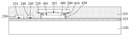
도 1 내지 도 3을 결부하여 참조하면, 도 2는 도 1에서의 하나의 감광성 칩의 확대도이고, 도 3은 도 1에서의 하나의 필터의 확대도이며, 용접 패드를 구비하는 감광성 칩(200) 및 필터(400)를 제공하고, 상기 감광성 칩(200)의 용접 패드를 향하는 상기 필터(400)를 상기 감광성 칩(200)에 장착한다.Referring to FIGS. 1 to 3, FIG. 2 is an enlarged view of one photosensitive chip in FIG. 1, and FIG. 3 is an enlarged view of one filter in FIG. 1, and a photosensitive chip having a welding pad ( 200) and a
상기 감광성 칩(200)은 이미지 센서 칩이고, 본 실시예에서, 상기 감광성 칩(200)은 CMOS 이미지 센서(CMOS image sensor, CIS) 칩이다. 다른 실시예에서, 상기 감광성 칩은 CCD(charge coupled device, 전하 결합 소자) 이미지 센서 칩일 수도 있다.The
본 실시예에서, 상기 감광성 칩(200)은 광 신호 수신면(201)(도 2에 도시된 바와 같음)을 구비하고, 상기 감광성 칩(200)은 상기 광 신호 수신면(201)을 통해 광 복사 신호를 수신하여 센싱한다. 구체적으로, 도 2에 도시된 바와 같이, 상기 감광성 칩(200)은 감광성 영역(200C) 및 상기 감광성 영역(200C)을 둘러싸는 주변 영역(200E)을 포함하고, 상기 광 신호 수신면(201)은 상기 감광성 영역(200C)에 위치한다.In this embodiment, the
상기 감광성 칩(200)은 복수개의 픽셀 유닛을 포함하므로, 감광성 칩(200)은 복수개의 반도체 감광 소자(미도시), 및 상기 반도체 감광 소자에 위치하는 복수개의 필터 코팅(filter coating)(미도시)을 포함하고, 필터 코팅은 광 신호 수신면(201)에 의해 수신된 광 신호를 선택적으로 흡수시키거나 통과시킨다. 상기 감광성 칩(200)은 필터 코팅에 위치하는 마이크로렌즈(210)를 더 포함하고, 마이크로렌즈(210)는 반도체 감광 소자와 일대일로 대응됨으로써, 수신된 광 복사 신호 광선을 반도체 감광 소자에 집광시킨다. 상기 광 신호 수신면(201)은 상응하게 상기 마이크로렌즈(210)의 최상면이다.Since the
상기 감광성 칩(200)은 일반적으로 실리콘 기판 칩이고, 집적 회로 제작 기술로 제작되며, 감광성 칩(200)은 감광성 칩(200)과 다른 칩 또는 부재의 전기적 연결을 실현하기 위한 용접 패드를 구비한다. 본 실시예에서, 상기 감광성 칩(200)은 주변 영역(200E)에 형성되는 제1 칩 용접 패드(220)를 구비한다. 구체적으로, 광 신호 수신면(201)의 동일 측에 위치하는 감광성 칩(200) 표면은 제1 칩 용접 패드(220)를 노출시킨다.The
상기 필터(400)는 상기 감광성 칩(200)에 장착되어 후속적인 패키징 공정이 광 신호 수신면(201)을 오염시키는 것을 방지하며, 후속적인 렌즈 모듈의 전체적인 두께를 감소시키는데 유리함으로써, 렌즈 모듈의 소형화, 박형화의 요구를 만족시킨다.The
상기 필터(400)는 적외선 필터 유리편 또는 전체 투과 유리편일 수 있다. 본 실시예에서, 상기 필터(400)는 적외선 필터 유리편이고, 입사광 중의 적외선이 감광성 칩(200) 성능에 미치는 영향을 제거한다.The
구체적으로, 상기 필터(400)는 적외선 차단 필터(infrared cut filter, IRCF)이고, 상기 적외선 차단 필터는 푸른색 유리 적외선 차단 필터일 수 있거나, 유리 및 상기 유리 표면에 위치하는 적외선 차단 코팅(IR cut coating)을 포함한다.Specifically, the
본 실시예에서, 상기 필터(400)는 조립면(401)(도 1에 도시된 바와 같음)을 포함한다. 상기 조립면(401)은 감광성 칩(200)과 장착되는 면이고, 즉, 상기 감광성 칩(200)을 향하는 면이다.In this embodiment, the
구체적으로, 필터(400)가 푸른색 유리 적외선 차단 필터일 경우, 푸른색 유리 적외선 차단 필터의 하나의 표면에는 반사 방지 코팅(reflection reducing coating) 또는 반사 방지막(antireflection coating)이 도금되어 있고, 반사 방지 코팅 또는 반사 방지막 표면과 등지는 면은 조립면(401)이다. 필터(400)가 유리 및 상기 표면에 위치하는 적외선 차단 코팅을 포함할 경우, 적외선 차단 코팅과 등지는 유리 표면은 조립면(401)이다. 다른 실시예에서, 필터가 전체 투과 유리편일 경우, 전체 투과 유리편의 어느 하나의 표면은 조립면이다.Specifically, when the
도 3에 도시된 바와 같이, 상기 필터(400)는 투광 영역(400C) 및 상기 투광 영역(400C)을 둘러싸는 가장자리 영역(400E)을 포함한다. 후속적으로 렌즈 모듈을 형성한 후, 상기 투광 영역(400C)은 외부의 입사광이 투과되도록 함으로써, 광 신호 수신면(201)이 광 신호를 수신하도록 하여 렌즈 모듈의 정상적인 사용 기능을 보장한다. 상기 가장자리 영역(400E)은 필터(400)와 감광성 칩(200)의 장착을 위해 공간 위치를 남겨둔다.As shown in FIG. 3, the
본 실시예에서, 상기 필터(400)를 상기 감광성 칩(200)에 장착한 후, 상기 필터(400)와 감광성 칩(200)은 감광성 유닛(250)(도 1에 도시된 바와 같음)을 구성한다.In this embodiment, after the
도 1에 도시된 바와 같이, 본 실시예에서, 상기 필터(400)는 접착 구조(410)를 통해 감광성 칩(200)에 장착되고, 상기 접착 구조(410)는 상기 광 신호 수신면(201)을 둘러싼다.1, in this embodiment, the
상기 접착 구조(410)는 필터(400)와 감광성 칩(200)을 물리적으로 연결시킨다. 또한, 상기 필터(400), 접착 구조(410) 및 감광성 칩(200)은 캐비티(미도시)를 이루어, 상기 필터(400)와 감광성 칩(200)의 직접적인 접촉을 방지함으로써, 상기 필터(400)가 감광성 칩(200)의 성능에 대해 나쁜 영향을 미치는 것을 방지한다.The
본 실시예에서, 상기 접착 구조(410)는 상기 광 신호 수신면(201)을 둘러쌈으로써, 광 신호 수신면(201) 상방의 필터(400)가 상기 감광성 칩(200)의 감광성 경로에 위치하도록 한다.In this embodiment, the
구체적으로, 상기 접착 구조(410)의 재료는 포토리소그래피 가능한 재료이므로, 포토리소그래피 공정을 이용하여 상기 접착 구조(410)를 형성할 수 있는데, 이는 접착 구조(410)의 형태 품질과 사이즈 정밀도를 향상시키고 패키징 효율과 생산 능력을 향상시키는데 유리할 뿐만 아니라, 접착 구조(410)의 접착 강도에 대한 영향을 감소시킬 수도 있다. 본 실시예에서, 상기 접착 구조(410)의 재료는 포토리소그래피 가능한 드라이 필름(dry film)이다. 다른 실시예에서, 상기 접착 구조의 재료는 포토리소그래피 가능한 폴리이미드(polyimide), 포토리소그래피 가능한 폴리벤즈옥사졸(PBO) 또는 포토리소그래피 가능한 벤조시클로부텐(BCB)일 수도 있다.Specifically, since the material of the
본 실시예에서, 접착 구조(410)를 형성하는 공정 난도를 감소시키고 접착 구조(410)의 형성이 광 신호 수신면(201)에 대한 영향을 감소시키기 위하여, 필터(400)에 상기 접착 구조(410)를 형성한다.In this embodiment, the
구체적으로, 도 1에 도시된 바와 같이, 상기 장착 단계는, 제3 캐리어 기판(340)을 제공하는 단계; 필터(400)의 조립면(401)을 등지는 면을 제3 캐리어 기판(340)에 임시 본딩시키는 단계; 상기 임시 본딩 단계 이후에 상기 필터(400)의 가장자리 영역(400E)에 고리형 접착 구조(410)를 형성하는 단계; 및 상기 감광성 칩(200)의 광 신호 수신면(201)이 고리형 접착 구조(410)를 향하도록 하여 상기 감광성 칩(200)의 주변 영역(200E)(도 2에 도시된 바와 같음)을 고리형 접착 구조(410)에 장착하여 감광성 유닛(250)을 형성하는 단계를 포함한다.Specifically, as shown in FIG. 1, the mounting step includes providing a
상기 제3 캐리어 기판(340)은 상기 접착 단계를 위해 공정 플랫폼을 제공함으로써, 공정 조작 가능성을 향상시킨다. 본 실시예에서, 상기 제3 캐리어 기판(340)은 캐리어 웨이퍼(carrier wafer)이다. 다른 실시예에서, 상기 제3 캐리어 기판은 다른 타입의 기판일 수도 있다.The
구체적으로, 제1 임시 본딩층(345)을 통해 필터(400)를 제3 캐리어 기판(340)에 임시 본딩시킨다. 상기 제1 임시 본딩층(345)은 박리층으로서, 후속적인 디본딩에 용이하다.Specifically, the
본 실시예에서, 상기 제1 임시 본딩층(345)은 발포막이다. 발포막은 대향되는 미세 접착면과 발포면을 포함하고, 발포막은 상온에서 접착성을 구비하며, 발포면은 제3 캐리어 기판(340)에 접착되므로, 후속적으로 발포막을 가열하여 발포면의 접착성을 제거함으로써 디본딩을 실현할 수 있다. 다른 실시예에서, 상기 제1 임시 본딩층은 다이 어태치 필름(die attach film, DAF)일 수도 있다.In this embodiment, the first
도 4를 결부하여 참조하면, 설명해야 할 점은, 상기 장착 단계 이후에, 상기 감광성 칩(200)의 광 신호 수신면(201)을 등지는 면을 UV 필름(310)에 접착시키는 단계; 및 상기 접착 단계 이후에 제1 디본딩 처리를 진행하여 상기 제3 캐리어 기판(340)(도 1에 도시된 바와 같음)을 제거하는 단계를 더 포함한다.Referring to FIG. 4, the point to be explained is, after the mounting step, bonding the surface facing the light
상기 접착 단계를 통해 후속적으로 감광성 유닛(250)(도 1에 도시된 바와 같음)을 다른 캐리어 기판에 임시 본딩시키는 것을 위해 공정 준비를 하고, 상기 UV 필름(310)은 제3 캐리어 기판(340)을 제거한 후 감광성 유닛(250)에 지지 작용과 고정 작용을 제공한다. 여기서, 자외선의 조사 하에 UV 필름(310)의 접착력은 감소될 수 있으므로, 후속적으로 상기 감광성 유닛(250)을 상기 UV 필름(310)으로부터 제거하는데 용이하다.Through the bonding step, a process is prepared for temporarily bonding the photosensitive unit 250 (as shown in FIG. 1) to another carrier substrate, and the
구체적으로, 라미네이터를 사용하여 상기 UV 필름(310)을 상기 감광성 칩(200)의 광 신호 수신면(201)을 등지는 면에 밀착시키고, 직경이 비교적 큰 프레임(315) 저부에 접착시키며, 상기 프레임(315)을 통해 필름을 팽팽하게 함으로써, 상기 감광성 유닛(250)이 상기 UV 필름(310)에 분립 고정되도록 한다. 본 실시예는 상기 UV 필름(310)과 프레임(315)을 더 구체적으로 설명하지 않는다.Specifically, using the laminator, the
본 실시예에서, 제1 임시 본딩층(345)(도 1에 도시된 바와 같음)은 발포막이므로, 제1 디본딩 처리의 단계에서, 제1 임시 본딩층(345)에 대해 열처리를 진행하여 발포막의 발포면의 접착성을 제거함으로써, 제3 캐리어 기판(340)을 제거하고, 이어서 떼어 내는 방식으로 제1 임시 본딩층(345)을 제거한다.In this embodiment, since the first temporary bonding layer 345 (as shown in FIG. 1) is a foamed film, heat treatment is performed on the first
도 5를 결부하여 참조하면, 설명해야 할 점은, 상기 패키징 방법은, 상기 필터(400)의 측벽을 커버하는 응력 완충층(420)을 형성하는 단계를 더 포함한다.Referring to FIG. 5, the point to be explained is that the packaging method further includes forming a
상기 응력 완충층(420)은 후속적으로 패키징층이 필터(400)에 대해 발생되는 응력을 감소시켜 상기 필터(400)가 파열되는 확률을 감소시킴으로써, 패키징 공정의 신뢰성 및 일드율(yield rate)을 향상시키고, 상응하게 렌즈 모듈의 신뢰성을 향상시킨다. 특히, 상기 필터(400)는 적외선 필터 유리편 또는 전체 투과 유리편이므로, 유리편이 응력 영향을 받아 파열되는 가능성이 높기에, 상기 응력 완충층(420)을 통해 필터(400)가 파열되는 확률을 현저히 감소시킬 수 있다.The
상기 응력 완충층(420)은 접착성을 구비하므로 필터(400)에서의 접착성을 보장한다. 본 실시예에서, 상기 응력 완충층(420)의 재료는 에폭시계 접착제이다. 에폭시계 접착제는 에폭시 수지 접착제(epoxy resin adhesive)이고, 에폭시계 접착제는 다양한 형태로 구현되며, 이의 성분을 개변시켜 상이한 탄성 계수의 재료를 획득할 수 있음으로써, 실제 정황에 따라, 상기 필터(400)가 받는 응력을 조절할 수 있다.Since the
본 실시예에서, 상기 응력 완충층(420)은 또한 접착 구조(410)의 측벽을 커버하여 패키징층이 접착 구조(410)에 대해 발생되는 응력을 감소시킴으로써, 패키징 공정의 신뢰성과 일드율을 더 향상시킨다.In this embodiment, the
본 실시예에서, 상기 감광성 칩(250)의 광 신호 수신면(201)을 등지는 면을 상기 UV 필름(310)에 접착한 후, 디스펜싱(dispensing) 공정을 통해 상기 응력 완충층(420)을 형성한다. 디스펜싱 공정을 선택하여 응력 완충층(420)을 형성하는 단계와 현재 패키징 공정의 호환성을 향상시키며, 공정이 간단하다.In this embodiment, after attaching the surface facing the light
다른 실시예에서, 감광성 칩과 필터를 합착하기 전에, 상기 응력 완충층을 형성할 수도 있다.In another embodiment, before bonding the photosensitive chip and the filter, the stress buffer layer may be formed.
도 6을 참조하면, 제1 캐리어 기판(320)을 제공하고, 상기 제1 캐리어 기판(320)에 기능 소자(미도시) 및 상기 필터(400)를 임시 본딩시키며, 상기 기능 소자는 용접 패드(미도시)를 구비하고, 상기 기능 소자의 용접 패드는 상기 제1 캐리어 기판(320)을 향한다.Referring to FIG. 6, a
기능 소자 및 감광성 칩(200)을 제1 캐리어 기판(320)에 임시 본딩시킴으로써, 후속적인 기능 소자와 감광성 칩(200)의 패키징 집적 및 전기학 집적을 위해 공정 준비를 한다.By temporarily bonding the functional element and the
임시 본딩(temporary bonding, TB) 방식을 통해 후속적으로 디본딩이 편리하다. 여기서. 상기 제1 캐리어 기판(320)은 또한 후속적인 패키징층의 형성에 공정 플랫폼을 제공한다.The subsequent bonding is convenient through the temporary bonding (TB) method. here. The
본 실시예에서, 상기 제1 캐리어 기판(320)은 캐리어 웨이퍼이다. 다른 실시예에서, 상기 제1 캐리어 기판은 다른 타입의 기판일 수도 있다In this embodiment, the
구체적으로, 제2 임시 본딩층(325)을 통해 필터(400) 및 기능 소자를 제1 캐리어 기판(320)에 임시 본딩시킨다. 상기 제2 임시 본딩층(325)에 대한 구체적인 설명은 전술한 제1 임시 본딩층(345)(도 1에 도시된 바와 같음)에 대한 상응한 설명을 참조할 수 있고, 여기서 더 설명하지 않도록 한다.Specifically, the
본 실시예에서, 필터(400)를 제1 캐리어 기판(320)에 임시 본딩시킨 후, 상기 감광성 칩(200)의 제1 칩 용접 패드(220)는 상기 제1 캐리어 기판(320)을 향한다.In this embodiment, after temporarily bonding the
구체적으로, 하나의 감광성 유닛(250)(도 1에 도시된 바와 같음) 위치의 UV 필름(310)(도 5에 도시된 바와 같음)에 대해 자외선을 조사하여 자외선 조사를 받은 UV 필름(310)의 접착성이 제거되고, 피어싱 핀을 통해 하나의 감광성 유닛(250)을 푸싱하며, 이어서 흡착 기기를 통해 상기 감광성 유닛(250)을 들어올리고, 상기 감광성 유닛(250)을 UV 필름(310)으로부터 순차적으로 박리시키고 상기 제1 캐리어 기판(320)의 기설정된 위치에 장착한다. 상기 감광성 유닛(250)을 하나씩 제1 캐리어 기판(320)에 장착하는 방식을 통해 감광성 유닛(250)이 상기 제1 캐리어 기판(320)에서의 위치 정밀도를 향상시키는데 유리하다.Specifically, the
본 실시예에서 하나의 감광성 유닛(250)만 설명하였다. 다른 실시예에서, 형성된 렌즈 모듈이 이중 촬영 또는 어레이 모듈 제품에 적용될 경우, 상기 감광성 유닛의 수량은 복수개일 수도 있다.In this embodiment, only one
설명해야 할 점은, 본 실시예에서, 상기 감광성 칩(200)과 필터(400)를 장착한 후, 상기 필터(400)를 제1 캐리어 기판(320)에 임시 본딩시킨다. 다른 실시예에서, 필터를 제1 캐리어 기판에 임시 본딩시킨 후, 상기 감광성 칩과 필터를 장착할 수도 있다.The point to be explained is that, in this embodiment, after the
상기 기능 소자는 촬영 어셈블리 중 감광성 칩(200)을 제외한 특정 기능 소자이고, 주변 칩(230) 및 수동 소자(240) 중 적어도 한 가지를 포함한다.The functional element is a specific functional element excluding the
본 실시예에서, 후속적으로 재배선 구조를 형성하는 공정 난도를 감소시키기 위하여, 기능 소자를 제1 캐리어 기판(320)에 임시 본딩시킨 후, 상기 기능 소자의 용접 패드는 제1 캐리어 기판(320)을 향한다.In this embodiment, after temporarily bonding the functional element to the
여기서, 필터(400)를 제1 캐리어 기판(320)에 임시 본딩시키고 각 기능 소자의 용접 패드가 제1 캐리어 기판(320)을 향하도록 함으로써, 감광성 칩(200)과 기능 소자의 두께 차이가 패키징층 형성 공정에 대한 영향을 방지할 수 있고, 후속적으로 패키징층을 형성하는 공정 복잡도를 감소시키는데 유리하다.Here, the thickness difference between the
본 실시예에서, 상기 기능 소자는 주변 칩(230) 및 수동 소자(240)를 포함한다.In this embodiment, the functional element includes a
상기 주변 칩(230)은 능동 소자이고, 후속적으로 감광성 칩(200)과 전기적으로 연결될 경우, 상기 감광성 칩(200)에 주변 회로를 제공하는데, 예를 들어, 아날로그 전력 공급 회로, 디지털 전력 공급 회로, 전압 완충 회로, 셔터 회로, 셔터 구동 회로 등을 제공한다.The
본 실시예에서, 상기 주변 칩(230)은 디지털 신호 프로세서 칩 및 메모리 칩 중 한 가지 또는 두 가지를 포함한다. 다른 실시예에서, 다른 기능 타입의 칩일 수도 있다. 도 6에서 하나의 주변 칩(230)만 도시하였지만, 주변 칩(230)의 수량은 하나에 한정되지 않는다.In this embodiment, the
상기 주변 칩(230)은 일반적으로 실리콘 기판 칩이고, 집적 회로 제작 기술로 제작되며, 상기 주변 칩(230)과 다른 칩 또는 부재의 전기적 연결을 실현하기 위한 용접 패드를 구비한다. 본 실시예에서, 상기 주변 칩(230)은 제2 칩 용접 패드(235)를 포함하고, 상기 주변 칩(230)이 제1 캐리어 기판(320)에 임시 본딩된 후, 상기 제2 칩 용접 패드(235)는 제1 캐리어 기판(320)을 향한다.The
상기 수동 소자(240)는 감광성 칩(200)의 감광성 작업에 대해 특정 작용을 한다. 상기 수동 소자(240)는 레지스터, 커패시턴스, 인덕턴스, 다이오드, 삼극관, 전위차계, 릴레이 또는 구동기 등 부피가 비교적 작은 전자 소자를 포함할 수 있다. 도 6에서 하나의 수동 소자(240)만 도시하였지만, 상기 수동 소자(240)의 수량은 하나에 한정되지 않는다.The
상기 수동 소자(240)도 상기 수동 소자(240)와 다른 칩 또는 부재의 전기적 연결을 실현하기 위한 용접 패드를 구비한다. 본 실시예에서, 상기 수동 소자(240)의 용접 패드는 전극(245)이고, 상기 수동 소자(240)를 제1 캐리어 기판(320)에 임시 본딩시킨 후, 상기 전극(245)은 제1 캐리어 기판(320)을 향한다.The
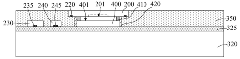
도 7 및 도 8을 결부하여 참조하면, 상기 제1 캐리어 기판(320) 및 기능 소자(미도시)를 커버하고 상기 감광성 칩(200)의 부분 측벽을 적어도 커버하는 패키징층(350)(도 8에 도시된 바와 같음)을 형성한다.Referring to FIGS. 7 and 8, a packaging layer 350 (FIG. 8) covering the
상기 패키징층(350)은 감광성 칩(200)과 기능 소자(예를 들어, 주변 칩(230), 수동 소자(240))에 대해 고정 작용을 하고, 감광성 칩(200)과 기능 소자에 대해 패키징 집적을 실현한다.The
여기서, 상기 패키징층(350)을 통해 렌즈 어셈블리 중 홀더가 차지하는 공간을 감소시킬 수 있을 뿐만 아니라, 회로기판(예를 들어, PCB)을 생략할 수 있음으로써, 후속적으로 형성된 렌즈 모듈의 전체 두께를 현저히 감소시켜, 렌즈 모듈의 소형화, 박형화의 요구를 만족시킨다. 또한, 기능 소자를 주변 메인보드에 장착하는 해결수단에 비해, 감광성 칩과 기능 소자를 모두 패키징층(350)에 집적시키는 방식은 감광성 칩(200)과 각 기능 소자 사이의 거리를 감소시키고, 상응하게 감광성 칩과 각 기능 소자 사이의 전기적 연결 거리를 단축시키는데 유리함으로써, 신호 전송 속도를 향상시키고, 렌즈 모듈의 사용 성능을 향상시킨다(예를 들어, 촬영 속도 및 저장 속도를 향상시킴).Here, through the
상기 패키징층(350)은 또한 절연, 밀봉 및 방습 작용이 있고, 렌즈 모듈의 신뢰성을 향상시키는데 유리하다.The
본 실시예에서, 상기 패키징층(350)의 재료는 에폭시 수지이다. 에폭시 수지는 수축률이 낮고, 접착성이 좋으며, 내부식성이 좋고, 전기적 특성이 우수하며 원가가 비교적 낮은 등 장점을 구비한다. 따라서 전자 소자와 집적 회로의 패키징 재료로서 광범위하게 사용된다.In this embodiment, the material of the
구체적으로, 사출성형(injection molding) 공정을 이용하여 상기 패키징층(350)을 형성한다. 사출성형 공정은 생산 속도가 빠르고, 효율이 높으며, 조작 자동화가 가능한 등 특징을 구비하고, 생산량을 향상시키고 공정 원가를 절감시키는데 유리하다. 다른 실시예에서, 다른 몰딩 공정을 이용하여 상기 패키징층을 형성할 수도 있다.Specifically, the
본 실시예에서, 상기 패키징층(350)을 형성하는 단계는, 상기 제1 캐리어 기판(320), 기능 소자 및 감광성 칩(200)을 커버하는 패키징 재료층(355)(도 7에 도시된 바와 같음)을 형성하는 단계; 상기 패키징 재료층(355)에 대해 연삭(grinding) 처리를 진행하여 상기 감광성 유닛(250) 및 기능 소자 중 높은 것과 서로 평행되는 상기 패키징층(350)을 형성하는 단계를 포함한다.In this embodiment, the step of forming the
상기 연삭 처리를 통해 상기 패키징층(350)의 두께가 작아지므로, 형성된 렌즈 모듈의 전체 두께를 감소시킨다.Since the thickness of the
필터(400)를 제1 캐리어 기판(320)에 임시 본딩시키므로, 상기 패키징 재료층(355)을 형성하는 과정에서, 사출성형 공정에 필요한 금형을 제작할 필요가 없으므로 공정이 간단하다.Since the
본 실시예에서, 상기 감광성 유닛(250)의 전체 두께는 기능 소자의 두께보다 크므로, 상기 연삭 처리 후, 상기 패키징층(350)의 제1 캐리어 기판(320)을 등지는 면과 감광성 칩(200)의 제1 캐리어 기판(320)을 등지는 면은 서로 평행되고, 즉, 상기 패키징층(350)은 상기 감광성 칩(200)의 측벽을 커버한다.In this embodiment, since the total thickness of the
본 실시예에서, 상기 패키징층(350)은 상응하게 필터(400)의 측벽을 더 커버함으로써, 감광성 유닛(250) 중 캐비티의 밀봉성을 향상시키며, 수증기, 산화 기체 등이 상기 캐비티 내에 들어가는 확률을 감소시켜 감광성 칩(200)의 성능을 보장한다. In this embodiment, the
설명해야 할 점은, 상기 패키징층(350)의 작용 하에, 회로기판을 생략함으로써, 렌즈 모듈의 두께를 감소시키는 효과를 발생하므로, 감광성 칩(200)과 주변 칩(230)에 대해 박화 처리를 진행할 필요가 없기에, 상기 감광성 칩(200)과 주변 칩(230)의 기계적 강도와 신뢰성을 향상시킨다. 다른 실시예에서, 공정 요구에 따라, 상기 감광성 칩과 주변 칩의 두께를 적절히 감소시킬 수 있지만, 이의 기계적 강도와 신뢰성이 영향을 받지 않도록 박화량이 비교적 작다.The point to be explained is that, under the action of the
도 9를 참조하면, 제2 디본딩 처리를 진행하여 상기 제1 캐리어 기판(320)(도 8에 도시된 바와 같음)을 제거한다.Referring to FIG. 9, a second debonding process is performed to remove the first carrier substrate 320 (as shown in FIG. 8 ).
상기 제1 캐리어 기판(320)을 제거하여 상기 기능 소자의 용접 패드를 노출시킴으로써, 후속적인 전기적 연결 공정을 위해 공정 준비를 한다.By removing the
본 실시예에서, 상기 제2 디본딩 처리의 단계는, 상기 제1 캐리어 기판(320) 및 제2 임시 본딩층(325)(도 8에 도시된 바와 같음)을 순차적으로 제거하는 단계를 포함한다. 상기 제2 디본딩 처리에 대한 구체적인 설명은 전술한 상기 제1 디본딩 처리에 대한 관련 설명을 참조할 수 있고, 여기서 더 설명하지 않도록 한다.In this embodiment, the step of the second debonding process includes sequentially removing the
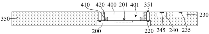
도 10 내지 도 14를 결부하여 참조하면, 상기 제1 캐리어 기판(320)(도 8에 도시된 바와 같음)을 제거한 후, 상기 패키징층(350)에서의 상기 필터(400)에 근접하는 일측에 상기 감광성 칩(200)의 용접 패드 및 상기 기능 소자(미도시)의 용접 패드(미도시)에 전기적으로 연결되는 재배선(redistribution layer, RDL) 구조(360)(도 14에 도시된 바와 같음)를 형성한다.Referring to FIGS. 10 to 14, after removing the first carrier substrate 320 (as shown in FIG. 8 ), on one side close to the
상기 재배선 구조(360)는 형성된 촬영 어셈블리의 전기학 집적을 실현한다. 여기서, 상기 패키징층(350) 및 재배선 구조(360)을 통해 감광성 칩(200)과 기능 소자 사이의 거리를 감소시키고, 상응하게 전기적 연결 거리를 단축시키므로, 신호를 전송하는 속도를 향상시킴으로써, 렌즈 모듈의 사용 성능을 향상시킨다. 구체적으로, 상기 주변 칩(230)은 디지털 신호 프로세서 칩 및 메모리 칩 중 한 가지 또는 두 가지를 포함하므로, 상응하게 촬영 속도 및 저장 속도를 향상시키는데 유리하다.The
또한, 재배선 구조(360)를 선택하여 상기 감광성 칩(200)과 기능 소자 사이의 거리를 감소시키는 동시에 전기적 연결 공정 가능성을 향상시킬 수 있고, 와이어 본딩 공정에 비해, 재배선 구조(360)는 대량 생산이 가능하여 패키징 효율을 향상시킬 수 있다.In addition, by selecting the
이 밖에, 상기 패키징층(350)에서의 필터(400)에 근접하는 일측에 상기 재배선 구조(360)를 형성하고, 후속적으로 렌즈 어셈블리를 상기 패키징층(350)에 조립한 후, 상기 재배선 구조(360)는 상응하게 렌즈 어셈블리의 홀더에 위치하여 재배선 구조(360)가 보호 받으므로, 렌즈 모듈의 신뢰성과 안정성을 향상시키는데 유리하고, 렌즈 모듈의 후속적인 패키징에 용이하다.In addition, the
본 실시예에서, 상기 재배선 구조(360)는 상기 제1 칩 용접 패드(220), 제2 칩 용접 패드(235) 및 전극(245)에 전기적으로 연결된다. 여기서, 상기 패키징층(350)은 상기 제2 칩 용접 패드(235) 및 전극(245)을 노출시키므로, 상기 재배선 구조(360)를 형성하는 공정이 비교적 간단하다.In this embodiment, the
구체적으로, 상기 재배선 구조(360)를 형성하는 단계는 하기와 같은 단계를 포함한다.Specifically, the step of forming the
도 10 및 도 11을 결부하여 참조하면, 상기 패키징층(350) 내에 상기 감광성 칩(200)의 용접 패드에 전기적으로 연결되는 전도성 칼럼(280)(도 11에 도시된 바와 같음)을 형성한다.Referring to FIGS. 10 and 11, a conductive column 280 (as shown in FIG. 11) electrically connected to a welding pad of the
상기 전도성 칼럼(280)은 상기 제1 칩 용접 패드(220)에 전기적으로 연결되어 상기 감광성 칩(200)의 외부 연결 전극으로 작용하고, 상기 감광성 칩(200)은 상기 전도성 칼럼(280)을 통해 기능 소자와 전기적으로 연결된다. 여기서, 상기 전도성 칼럼(280)은 상기 감광성 칩(200) 중의 금속 연결 구조와 전기적으로 연결될 수 있고, 상기 감광성 칩(200)을 관통하여 상기 제1 칩 용접 패드(220)와 직접 전기적으로 연결될 수도 있다.The
상기 전도성 칼럼(280)의 최상면은 상기 패키징층(350)에 노출되고, 상기 전도성 칼럼(280)을 통해 상기 감광성 칩(200)의 외부 연결 전극과 기능 소자의 용접 패드가 상기 패키징층(350)의 동일측에 위치하도로 함으로써, 상기 재배선 구조를 형성하는 공정 난도를 감소시킨다. 상기 전도성 칼럼(280)의 최상면은 상기 전도성 칼럼(280)의 연장 방향을 따라 상기 전도성 칼럼(280)이 감광성 칩(200)을 등지는 면을 의미한다.The top surface of the
본 실시예에서, 상기 전도성 칼럼(280)의 재료는 구리이므로, 상기 전도성 칼럼(280)의 전도성을 향상시키고, 상기 전도성 칼럼(280)의 공정 난도를 감소시킨다. 다른 실시예에서, 상기 전도성 칼럼의 재료는 텅스텐(tungsten)과 같은 다른 적용 가능한 전도성 재료일 수 있다.In this embodiment, since the material of the
구체적으로, 전도성 칼럼(280)을 형성하는 단계는, 상기 패키징층(350)을 패턴화하여 상기 패키징층(350) 내에 제1 칩 용접 패드(220)를 노출시키는 전도성 관통홀(351)(도 10에 도시된 바와 같음)을 형성하는 단계; 및 상기 전도성 관통홀(351) 내에 상기 전도성 칼럼(280)을 형성하는 단계를 포함한다.Specifically, the step of forming the
본 실시예에서, 식각 공정을 통해 상기 전도성 관통홀(351)을 형성한다. 구체적으로, 레이저 식각 공정을 통해 상기 패키징층(350)을 식각하여 상기 전도성 관통홀(351)을 형성한다. 레이저 식각 공정은 정밀도가 비교적 높으므로, 상기 전도성 관통홀(351)의 형성 위치와 사이즈를 비교적 정밀하게 결정할 수 있다.In this embodiment, the conductive through
본 실시예에서, 전기도금 공정을 통해 상기 전도성 관통홀(351) 내에 상기 전도성 칼럼(280)을 형성한다.In this embodiment, the
전도성 칼럼을 전도성 관통홀 내에 본딩시키는 해결수단에 비해, 본 실시예의 충진 방식을 통해 상기 전도성 관통홀(351) 내에 전도성 칼럼(280)을 형성하는 해결수단은 전도성 칼럼(280)을 형성하는 공정 난도를 감소시키고, 정렬 문제가 발생되는 것을 방지하며, 전도성 칼럼(280)과 제1 칩 용접 패드(220)의 전기적 연결 신뢰성을 향상시킨다.Compared to a solution for bonding a conductive column in a conductive through hole, a solution for forming a
도 12 내지 도 14를 결부하여 참조하면, 상기 패키징층(350)에서의 상기 필터(400)에 근접하는 일측에 상기 전도성 칼럼(280) 및 기능 소자의 용접 패드에 전기적으로 연결되는 연결선(290)을 형성한다.Referring to FIGS. 12 to 14, a
본 실시예에서, 상기 연결선(290)을 형성하는 단계는 하기와 같은 단계를 포함한다.In this embodiment, the step of forming the connecting
도 12에 도시된 바와 같이, 상기 연결선(290)이 형성되는 제2 캐리어 기판(330)을 제공한다.12, a
구체적으로, 상기 제2 캐리어 기판(330)에 제3 임시 본딩층(331)을 형성하고; 제3 임시 본딩층에 제1 매질층(332)을 형성하며; 제1 매질층(332)을 패턴화하여 상기 제1 매질층(332) 내에 제1 연결홈(미도시)을 형성하고; 상기 제1 연결홈 내에 상기 연결선(290)을 형성한다.Specifically, forming a third
본 실시예에서, 상기 연결선(290)은 상기 제1 연결홈 내에 충진되므로, 상응하게 상기 연결선(290)을 형성하는 공정 복잡도를 감소시킨다.In this embodiment, since the connecting
여기서, 상기 제3 임시 본딩층(331)은 박리층으로서, 후속적으로 상기 연결선(290)과 제2 캐리어 기판(330)의 분리에 용이하다. 본 실시예에서, 상기 제3 임시 본딩층(331)은 발포막일 수 있고, 상기 제3 임시 본딩층(331)에 대한 구체적인 설명은 전술한 제2 임시 본딩층(345)(도 1에 도시된 바와 같음)에 대한 상응한 설명을 참조할 수 있고, 여기서 더 설명하지 않도록 한다.Here, the third
상기 제1 매질층(332) 내의 제1 연결홈은 상기 연결선(290)의 형상, 위치 및 사이즈를 정의하기 위한 것이다. 본 실시예에서, 상기 제1 매질층(332)의 재료는 감광성 재료이고, 상응하게 포토리소그래피 공정을 통해 패턴화할 수 있다. 구체적으로, 상기 제1 매질층(332)의 재료는 감광성 폴리이미드, 감광성 벤조시클로부텐 또는 감광성 폴리벤즈옥사졸이다.The first connection groove in the first
전술한 재료의 제1 매질층(332)은 비교적 강한 내부식성을 구비하므로, 상기 연결선(290)을 형성한 후, 반응 이온 식각 공정을 이용하여 상기 제1 매질층(332)을 제거함으로써, 후속적인 전기적 연결 공정을 위해 공정 기초를 제공한다.Since the first
설명해야 할 점은, 다른 실시예에서, 상기 제2 캐리어 기판에 제3 임시 본딩층을 형성하는 단계 이전에, 상기 제2 캐리어 기판에 패시베이션층을 형성하는 단계를 더 포함한다. 상기 패시베이션층을 통해 상기 제2 캐리어 기판이 오염되는 것을 방지함으로써, 상기 제2 캐리어 기판이 재이용될 수 있도록 한다. 본 실시예에서, 상기 패시베이션층의 재료는 산화 규소 또는 질화 규소일 수 있다.It should be noted that, in another embodiment, prior to forming a third temporary bonding layer on the second carrier substrate, further comprising forming a passivation layer on the second carrier substrate. By preventing the second carrier substrate from being contaminated through the passivation layer, the second carrier substrate can be reused. In this embodiment, the material of the passivation layer may be silicon oxide or silicon nitride.
더 설명해야 할 점은, 다른 실시예에서, 상기 연결선으로서 식각을 통해 패턴화가 용이한 재료(예를 들어, 알루미늄)를 선택할 경우, 식각 방식을 통해 상기 연결선을 형성할 수도 있다. 상응하게, 상기 연결선을 형성하는 단계는, 상기 제3 임시 본딩층에 전도층을 형성하는 단계; 및 상기 전도층을 식각하여 연결선을 형성하는 단계를 포함한다.Further, in another embodiment, when a material (for example, aluminum) that is easily patterned through etching is selected as the connection line, the connection line may be formed through an etching method. Correspondingly, forming the connecting line may include forming a conductive layer on the third temporary bonding layer; And forming a connection line by etching the conductive layer.
도 13 및 도 14에 도시된 바와 같이, 본 실시예에서, 상기 재배선 구조(360)(도 14에 도시된 바와 같음)을 형성하는 단계는, 상기 전도성 칼럼(280) 및 기능 소자의 용접 패드에 전도성 돌출 블록(365)을 형성하는 단계; 및 상기 연결선(290)을 상기 전도성 돌출 블록(365)에 본딩시켜 상기 전도성 돌출 블록(365)과 전기적으로 연결시키는 단계를 더 포함한다.13 and 14, in this embodiment, forming the redistribution structure 360 (as shown in FIG. 14) includes welding pads of the
상기 전도성 칼럼(280), 전도성 돌출 블록(365) 및 연결선(290)은 상기 재배선 구조(360)를 구성한다.The
상기 전도성 돌출 블록(365)은 전도성 칼럼(280), 제2 칩 용접 패드(235) 및 전극(245)에 돌출되고, 상기 전도성 돌출 블록(365)을 통해 연결선(290)과 전도성 칼럼(280), 제2 칩 용접 패드(235) 및 전극(245) 사이의 본딩 신뢰성을 향상시킨다.The
또한, 전도성 칼럼(280), 제2 칩 용접 패드(235) 및 전극(245)에 전도성 돌출 블록(365)을 형성하는 방식은 전도성 돌출 블록(365)의 위치 정밀도를 향상시키는데 유리하고, 상기 전도성 돌출 블록(365)을 형성하는 공정 난도를 감소시킨다.In addition, the method of forming the
본 실시예에서, 범핑(bumping) 공정을 이용하여 상기 전도성 돌출 블록(365)을 형성한다. 범핑 공정을 선택하면 각 칩 및 소자와 상기 재배선 구조(360) 사이의 신호 전송 신뢰성을 향상시키는데 유리하다. 구체적으로, 상기 전도성 돌출 블록(365)의 재료는 주석일 수 있다.In this embodiment, the
본 실시예에서, 금속 본딩 공정을 이용하여 연결선(290)을 전도성 돌출 블록(365)에 본딩시킨다.In this embodiment, the connecting
구체적으로, 상기 금속 본딩 공정은 열압축 본딩 공정이다. 상기 금속 본딩 공정에서, 연결선(290)과 전도성 돌출 블록(365)의 접촉면은 압력의 작용 하에 소성 변형을 일으켜 접촉면의 원자가 서로 접촉되도록 하고, 본딩 온도가 상승함에 따라 접촉면의 원자의 확산이 가속화되어 크로스오버 확산이 이루어진다. 일정한 본딩 시간에 도달한 후, 접촉면의 결정 격자는 재조합됨으로써 본딩이 이루어지고, 본딩 강도, 전기전도 열전도성, 전계확산 내성 및 기계적 연결 성능이 비교적 높다.Specifically, the metal bonding process is a thermal compression bonding process. In the metal bonding process, the contact surface of the connecting
설명해야 할 점은, 본딩 온도가 상승함에 따라, 접촉면의 원자는 보다 많은 에너지를 획득하고, 원자 사이의 확산은 보다 더 현저하며, 본딩 온도의 상승은 결정립 성장을 촉진시킬 수 있고, 에너지를 획득한 결정립은 크로스오버 성장할 수 있으므로, 경계면을 제거하는데 유리함으로써, 접촉면의 재료가 일체가 되도록 한다. 하지만, 본딩 온도가 지나치게 높으면, 상기 감광성 칩(200)과 주변 칩(230), 특히 형성된 촬영 어셈블리 중의 감광 소자의 성능에 대해 나쁜 영향을 미치고, 공정 온도가 지나치게 높으면 열응력이 발생할 수도 있어 정렬 정밀도가 저하되고 공정 원가가 증가되며 생산 효율이 감소되는 등 문제가 발생한다. 이에, 본 실시예에서, 상기 금속 본딩 공정은 금속 저온 본딩 공정이고, 상기 금속 본딩 공정의 본딩 온도는 250 ℃보다 작거나 같다. 여기서, 본딩 온도의 최소값은 본딩이 가능하기만 하면 된다.It should be explained that as the bonding temperature increases, atoms on the contact surface acquire more energy, diffusion between atoms is more remarkable, and an increase in bonding temperature can promote grain growth and acquire energy Since one crystal grain can grow crossover, it is advantageous to remove the interface, so that the material of the contact surface is integral. However, if the bonding temperature is too high, the
상기 본딩 온도의 설정 하에, 압력을 증가시켜 원자 사이의 확산이 보다 더 용이하도록 함으로써, 상기 연결선(290)과 전도성 돌출 블록(365)의 본딩 품질을 향상시킨다. 이에, 본 실시예에서, 상기 금속 본딩 공정의 압력은 200 kPa보다 크거나 같다. 여기서, 상기 압력은 압착 도구에 의해 발생된다.Under the setting of the bonding temperature, the pressure is increased to make diffusion between atoms easier, thereby improving the bonding quality of the connecting
본딩 시간도 본딩 품질을 증가시킬 수 있다. 이에, 본 실시예에서, 상기 금속 본딩 공정의 본딩 시간은 30 분보다 크거나 같다.Bonding time can also increase bonding quality. Thus, in this embodiment, the bonding time of the metal bonding process is greater than or equal to 30 minutes.
설명해야 할 점은, 실제 공정에서, 상기 본딩 온도, 압력 및 본딩 시간을 합리적으로 조절하고 서로 배합하여 금속 본딩 품질과 효율을 보장할 수 있다. 더 설명해야 할 점은, 접촉면이 산화되거나 오염되는 확률을 감소시키기 위하여, 진공 환경에서 상기 금속 본딩 공정을 진행할 수 있다.The point to be explained is that in the actual process, the bonding temperature, pressure and bonding time can be reasonably controlled and blended with each other to ensure metal bonding quality and efficiency. Further, to reduce the probability that the contact surface is oxidized or contaminated, the metal bonding process may be performed in a vacuum environment.
더 설명해야 할 점은, 다른 실시예에서, 상기 제2 캐리어 기판에 상기 연결선을 형성한 후, 상기 연결선에 상기 전도성 돌출 블록을 형성할 수도 있다. 상응하게, 금속 본딩 공정을 이용하여 상기 전도성 돌출 블록을 대응되는 상기 전도성 칼럼 및 기능 소자의 용접 패드에 본딩시키고, 상기 전도성 칼럼, 전도성 돌출 블록 및 연결선은 상기 재배선 구조를 구성한다.Further, in another embodiment, after forming the connection line on the second carrier substrate, the conductive protrusion block may be formed on the connection line. Correspondingly, using the metal bonding process, the conductive projecting blocks are bonded to the corresponding welding pads of the conductive columns and functional elements, and the conductive columns, conductive projecting blocks and connecting lines constitute the redistribution structure.
상기 실시예에서, 상기 연결선에 전도성 돌출 블록을 형성하는 단계는, 상기 제2 캐리어 기판 및 연결선을 커버하는 제2 매질층을 형성하는 단계; 상기 제2 매질층을 패턴화하여 상기 제2 매질층 내에 연결 관통홀을 형성하고 상기 연결선의 일부분을 노출시키는 단계; 전기도금 공정을 이용하여 상기 연결 관통홀 내에 상기 전도성 돌출 블록을 형성하는 단계; 및 상기 제2 매질층을 제거하는 단계를 포함한다.In the above embodiment, the step of forming a conductive protruding block on the connecting line includes: forming a second medium layer covering the second carrier substrate and the connecting line; Patterning the second medium layer to form a connection through hole in the second medium layer and exposing a portion of the connection line; Forming the conductive protrusion block in the connection through-hole using an electroplating process; And removing the second medium layer.
상응하게, 상기 전도성 돌출 블록의 재료는 상기 전도성 칼럼 및 연결층의 재료와 동일할 수 있다.Correspondingly, the material of the conductive protrusion block may be the same as the material of the conductive column and the connecting layer.
상기 전도성 돌출 블록을 형성한 후, 반응 이온 식각 공정을 이용하여 상기 제2 매질층을 제거한다.After forming the conductive protrusion block, the second medium layer is removed using a reaction ion etching process.
상기 제2 매질층에 대한 설명은 전술한 제1 매질층의 상응한 설명을 참조할 수 있고, 여기서 더 설명하지 않도록 한다.For the description of the second medium layer, reference may be made to the corresponding description of the first medium layer described above, and will not be described further herein.
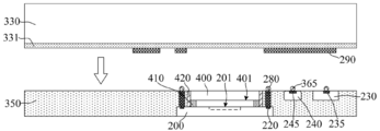
본 실시예에서, 상기 재배선 구조(360)를 형성한 후, 제3 디본딩 처리를 진행하여 상기 제2 캐리어 기판(330) 및 제3 임시 본딩층(331)을 제거한다. 상기 제3 디본딩 처리에 대한 구체적인 설명은 제1 디본딩 처리에 대한 관련 설명을 참조할 수 있고, 여기서 더 설명하지 않도록 한다.In this embodiment, after the
도 15를 결부하여 참조하면, 상기 제3 디본딩 처리 단계 이후에, 상기 패키징층(350)에 대해 다이싱(dicing) 처리를 진행하는 단계를 더 포함한다.Referring to FIG. 15, after the third debonding process step, further comprising a step of performing a dicing process on the
상기 다이싱 처리를 통해 사이즈가 공정 요구에 부합되는 하나의 촬영 어셈블리(260)를 형성함으로써, 후속적으로 렌즈 어셈블리를 장착하기 위해 공정 준비를 한다. 본 실시예에서, 레이저 절단 공정을 이용하여 상기 다이싱 처리를 진행한다.Through the dicing process, a
도 16을 결부하여 참조하면, 상기 재배선 구조(360)를 형성하는 단계 이후에, 상기 재배선 구조(360)에 연성회로기판(FPC, flexible printed circuit board)(510)을 본딩시키는 단계를 더 포함한다.Referring to FIG. 16, after the step of forming the
상기 연성회로기판(FPC)(510)은 회로기판을 생략할 경우 상기 촬영 어셈블리(260)와 후속적인 렌즈 어셈블리 사이의 전기적 연결, 및 형성된 렌즈 모듈과 다른 소자 사이의 전기적 연결을 실현한다. 후속적으로 렌즈 모듈을 형성한 후, 상기 렌즈 모듈도 상기 연성회로기판(FPC)(510)을 통해 전자 기기 중 다른 소자와 전기적으로 연결될 수 있음으로써, 전자 기기의 정상적인 촬영 기능을 실현한다.When the circuit board is omitted, the flexible circuit board (FPC) 510 realizes an electrical connection between the
본 실시예에서, 상기 연성회로기판(FPC)(510)에 회로 구조가 구비되므로, 금속 본딩 공정을 통해 상기 연성회로기판(FPC)(510)을 상기 재배선 구조(360)에 본딩시킴으로써, 전기적 연결을 실현한다. 구체적으로, 상기 연성회로기판(FPC)(510)을 상기 연결선(290)에 본딩시킨다.In this embodiment, since the circuit structure is provided on the flexible circuit board (FPC) 510, by bonding the flexible circuit board (FPC) 510 to the
본 실시예에서, 공정 가능성을 향상시키기 위하여, 상기 제3 디본딩 처리 및 다이싱 처리 후, 상기 재배선 구조(360)에 상기 연성회로기판(FPC)(510)을 본딩시킨다.In this embodiment, to improve processability, after the third debonding process and dicing process, the flexible circuit board (FPC) 510 is bonded to the
설명해야 할 점은, 상기 연성회로기판(FPC)(510)에 상기 연성회로기판(FPC)(510)과 다른 회로 소자를 전기적으로 연결시키는 커넥터(connector)(520)가 형성된다. 렌즈 모듈이 전자 기기에 적용될 경우, 상기 커넥터(520)는 상기 전자 기기의 메인보드에 전기적으로 연결됨으로써, 상기 렌즈 모듈과 상기 전자 기기 중 다른 소자 사이의 정보 전송을 실현하고, 상기 렌즈 모듈의 이미지 정보를 상기 전자 기기에 전달한다. 구체적으로, 상기 커넥터(520)는 골드핑거 커넥터일 수 있다.The point to be explained is that a
도 17 내지 도 20은 본 발명에 따른 촬영 어셈블리의 패키징 방법의 다른 일 실시예에서의 각 단계에 대응되는 구조 모식도이다.17 to 20 are structural schematic diagrams corresponding to each step in another embodiment of the packaging method of the imaging assembly according to the present invention.
본 실시예와 전술한 실시예의 동일한 부분은 여기서 더 설명하지 않도록 한다. 본 실시예와 전술한 실시예의 상이한 부분은, 상기 재배선 구조(360a)를 형성하는 단계는 동일한 단계에서 상기 전도성 칼럼(280a) 및 연결선(290a)을 형성하는 단계를 포함하는 것이다.The same parts of this embodiment and the above-described embodiment will not be described further herein. Different parts of the present embodiment and the above-described embodiment, forming the
구체적으로, 도 17을 참조하면, 상기 패키징층(250a)을 패턴화하여 상기 패키징층(250a) 내에 상기 제1 칩 용접 패드(220a)를 노출시키는 전도성 관통홀(351a)을 형성한다.Specifically, referring to FIG. 17, the packaging layer 250a is patterned to form a conductive through
본 실시예에서, 레이저 식각 공정을 통해 상기 전도성 관통홀(351a)을 형성한다. 상기 전도성 관통홀(351a)을 형성하는 단계에 대한 구체적인 설명은 전술한 실시예에서의 상응한 설명을 참조할 수 있고, 여기서 더 설명하지 않도록 한다.In this embodiment, the conductive through
도18을 참조하면, 상기 패키징층(350a), 필터(미도시) 및 기능 소자(미도시)를 커버하고 전도성 관통홀(351a) 내에 위치하는 제3 매질층(332a)을 형성하고; 상기 제3 매질층(332a)을 패턴화하여 상기 전도성 관통홀(351a) 내에 위치하고 상기 패키징층(350a) 최상부의 부분 영역보다 높은 제3 매질층(332a)을 제거하고, 상기 제3 매질층 내에 제2 연결홈(338a)을 형성하며, 상기 제2 연결홈(338a)은 상기 제2 칩 용접 패드(235a) 및 전극(245a)을 노출시키고, 상기 제2 연결홈(338a)과 상기 전도성 관통홀(351a)을 전기적으로 연결시킨다.Referring to FIG. 18, a third
상기 제3 매질층(332a)에 대한 구체적인 설명은 전술한 실시예에서의 제1 매질층에의 상응한 설명을 참조할 수 있고, 여기서 더 설명하지 않도록 한다.For a detailed description of the third
도 19를 참조하면, 상기 제2 연결홈(338a)(도 18에 도시된 바와 같음) 및 전도성 관통홀(351a)(도 18에 도시된 바와 같음) 내에 전도성 재료를 충진하고, 상기 전도성 관통홀(351a) 내에 전도성 칼럼(280a)을 형성하며, 상기 제2 연결홈(338a) 내에 연결선(290a)을 형성하고, 상기 연결선(290a)과 전도성 칼럼(280a)은 일체화 구조의 상기 재배선 구조(360a)를 구성한다.Referring to FIG. 19, a conductive material is filled in the
본 실시예에서, 전기도금 공정을 통해 상기 전도성 관통홀(351a) 내에 전도성 칼럼(280a)을 형성하고, 상기 제2 연결홈(338a) 내에 연결선(290a)을 형성한다.In this embodiment, a
도 20을 참조하면, 상기 제3 매질층(332a)(도 19에 도시된 바와 같음)을 제거한다.Referring to FIG. 20, the third
본 실시예에서, 반응 이온 식각 공정을 이용하여 상기 제3 매질층(332a)을 제거한다.In this embodiment, the third
본 실시예에 따른 패키징 방법에 대한 구체적인 설명은 전술한 실시예에서의 상응한 설명을 참조할 수 있고, 여기서 더 설명하지 않도록 한다.For a detailed description of the packaging method according to the present embodiment, reference may be made to the corresponding description in the above-described embodiment, and will not be described further herein.
상응하게, 본 발명의 실시예는 촬영 어셈블리를 더 제공한다. 계속하여 도 16을 참조하면, 본 발명에 따른 촬영 어셈블리의 일 실시예의 구조 모식도를 나타낸다.Correspondingly, embodiments of the present invention further provide an imaging assembly. Continuing with reference to FIG. 16, there is shown a structural schematic diagram of an embodiment of the imaging assembly according to the present invention.
상기 촬영 어셈블리(260)는 패키징층(350), 상기 패키징층(350)에 삽입되는 감광성 유닛(250)(도 1에 도시된 바와 같음), 기능 소자(미도시) 및 재배선 구조(360)를 포함하되, 상기 감광성 유닛(250)은 감광성 칩(200) 및 상기 감광성 칩(200)에 장착되는 필터(400)를 포함하고, 상기 패키징층(350)의 최상면은 상기 필터(400) 및 기능 소자를 노출시키며, 상기 패키징층(350)의 저면은 상기 기능 소자보다 높고, 상기 패키징층(350)은 상기 감광성 칩(200)의 부분 측벽을 적어도 커버하며, 여기서, 상기 감광성 칩(200) 및 기능 소자는 모두 용접 패드를 구비하고, 상기 감광성 칩(200)의 용접 패드는 상기 패키징층(350)의 최상면을 향하며, 상기 기능 소자의 용접 패드는 상기 패키징층(350)의 최상면에 노출되고, 상기 재배선 구조(360)는 상기 패키징층(350)에서의 상기 필터(400)에 근접하는 일측에 위치하고, 상기 재배선 구조(360)는 상기 용접 패드에 전기적으로 연결된다.The
상기 패키징층(350)은 감광성 칩(200) 및 기능 소자에 대해 고정 작용을 하고, 감광성 칩(200) 및 기능 소자에 대해 패키징 집적을 실현한다. 여기서, 상기 패키징층(350)을 통해 렌즈 어셈블리 중 홀더가 차지하는 공간을 감소시킬 수 있을 뿐만 아니라, 회로기판을 생략할 수 있음으로써, 상기 렌즈 모듈의 전체 두께를 현저히 감소시켜, 렌즈 모듈의 소형화, 박형화의 요구를 만족시킨다.The
상기 패키징층(350)의 재료는 몰딩 재료이고, 상기 패키징층(350)은 또한 절연, 밀봉 및 방습 작용이 있으므로, 렌즈 모듈의 신뢰성을 향상시키는데 유리하다. 본 실시예에서, 상기 패키징층(350)의 재료는 에폭시 수지이다.The material of the
본 실시예에서, 상기 패키징층(350)은 대향되는 최상면과 저면을 포함한다. 여기서, 상기 패키징층(350)의 최상면은 렌즈 어셈블리를 장착하기 위한 면이다.In this embodiment, the
본 실시예에서, 상기 패키징층(350)의 저면은 상기 감광성 유닛(250) 및 기능 소자 중 높은 것과 서로 평행된다. 상응하게, 상기 패키징층(350)의 형성 공정이 감광성 칩(200)과 기능 소자 사이의 두께 차이의 영향을 받는 것을 방지하고, 상기 패키징층(350)을 형성하는 과정에서, 금형을 제작할 필요가 없으므로 공정이 간단하다.In this embodiment, the bottom surface of the
본 실시예에서, 상기 감광성 유닛(250)의 전체 두께는 기능 소자의 두께보다 크므로, 상기 패키징층(350)의 저면과 상기 감광성 칩(200)의 상기 필터(400)를 등지는 면은 한 평면에 있고, 즉, 상기 패키징층(350)은 상기 감광성 칩(200)의 측벽을 커버한다.In this embodiment, since the total thickness of the
또한, 상기 패키징층(350)은 필터(400)의 측벽을 더 커버함으로써, 감광성 유닛(250) 중 캐비티의 밀봉성을 향상시키며, 수증기, 산화 기체 등이 상기 캐비티 내에 들어가는 확률을 감소시켜 감광성 칩(200)의 성능을 보장한다.In addition, the
상기 감광성 칩(200)은 이미지 센서 칩이다. 본 실시예에서, 상기 감광성 칩(200)은 CMOS 이미지 센서 칩이다. 다른 실시예에서, 상기 감광성 칩은 CCD 이미지 센서 칩일 수도 있다.The
본 실시예에서, 상기 감광성 칩(200)은 감광성 영역(200C)(도 2에 도시된 바와 같음) 및 상기 감광성 영역(200C)을 둘러싸는 주변 영역(200E)(도 2에 도시된 바와 같음)을 포함하고, 상기 감광성 칩(200)은 상기 감광성 영역(200C)에 위치하는 광 신호 수신면(201)을 더 구비한다.In this embodiment, the
상기 감광성 칩(200)은 일반적으로 실리콘 기판 칩이고, 감광성 칩(200)의 용접 패드는 감광성 칩(200)과 다른 칩 또는 부재의 전기적 연결을 실현하기 위한 것이다. 본 실시예에서, 상기 감광성 칩(200)은 주변 영역(200E)에 위치하는 제1 칩 용접 패드(220)를 구비하고, 제1 칩 용접 패드(220)는 패키징층(350)의 최상면을 향한다.The
상기 필터(400)를 감광성 칩(200)에 장착하여 패키징 공정이 광 신호 수신면(201)을 오염시키는 것을 방지하고, 렌즈 모듈의 전체적인 두께를 감소시켜 렌즈 모듈의 소형화, 박형화의 요구를 만족시킨다.The
렌즈 모듈의 정상적인 기능을 실현하기 위하여, 상기 필터(400)는 적외선 필터 유리편 또는 전체 투과 유리편일 수 있다. 본 실시예에서, 상기 필터(400)는 적외선 필터 유리편이고, 입사광 중의 적외선이 상기 감광성 칩(200) 성능에 대한 영향을 제거하며, 이미징 효과 향상에 유리하다.In order to realize the normal function of the lens module, the
본 실시예에서, 상기 필터(400)는 접착 구조(410)를 통해 상기 감광성 칩(200)에 장착되고, 상기 접착 구조(410)는 광 신호 수신면(201)을 둘러싼다. 상기 접착 구조(410)는 필터(400)와 감광성 칩(200)을 물리적으로 연결시킨다. 필터(400)와 감광성 칩(200)의 직접적인 접촉을 방지함으로써, 감광성 칩(200)의 광학 성능에 대해 나쁜 영향을 미치는 것을 방지한다.In this embodiment, the
본 실시예에서, 상기 접착 구조(410)의 재료는 포토리소그래피 가능한 드라이 필름이다. 다른 실시예에서, 상기 접착 구조의 재료는 포토리소그래피 가능한 폴리이미드, 포토리소그래피 가능한 폴리벤즈옥사졸 또는 포토리소그래피 가능한 벤조시클로부텐일 수도 있다.In this embodiment, the material of the
본 실시예에서, 상기 접착 구조(410)는 상기 광 신호 수신면(201)을 둘러쌈으로써, 상기 광 신호 수신면(201) 상방의 필터(400)가 상기 감광성 칩(200)의 감광성 경로에 위치하도록 하여, 상기 감광성 칩(200)의 성능을 보장한다.In this embodiment, the
설명해야 할 점은, 본 실시예에서 하나의 감광성 유닛(250)만 설명하였다. 다른 실시예에서, 렌즈 모듈이 이중 촬영 또는 어레이 모듈 제품에 적용될 경우, 감광성 유닛의 수량은 복수개일 수도 있다.It should be noted that only one
더 설명해야 할 점은, 패키징층(350)은 필터(400)의 측벽을 커버하므로, 상기 촬영 어셈블리(260)는 상기 패키징층(350)과 필터(400)의 측벽 사이에 위치하는 응력 완충층(420)을 더 포함한다. 상기 응력 완충층(420)은 패키징층(350)이 필터(400)에 대해 발생되는 응력을 감소시키는데 유리하여, 상기 필터(400)가 파열되는 확률을 감소시킴으로써, 렌즈 모듈의 신뢰성을 향상시킨다.Further, since the
본 실시예에서, 상기 응력 완충층(420)의 재료는 에폭시계 접착제이다. In this embodiment, the material of the
본 실시예에서, 상기 응력 완충층(420)은 또한 상기 패키징층(350)과 상기 접착 구조(410)의 측벽 사이에 위치함으로써, 상기 패키징층(350)이 상기 접착 구조(410)에 대해 발생되는 응력을 감소시키므로, 상기 촬영 어셈블리(260)의 신뢰성과 일드율을 더 향상시키는데 유리하다.In this embodiment, the
상기 기능 소자는 촬영 어셈블리 중 상기 감광성 칩(200)을 제외한 특정 기능 소자이고, 주변 칩(230) 및 수동 소자(240) 중 적어도 한 가지를 포함한다.The functional element is a specific functional element excluding the
본 실시예에서, 상기 기능 소자는 주변 칩(230) 및 수동 소자(240)를 포함한다. In this embodiment, the functional element includes a
본 실시예에서, 상기 기능 소자의 용접 패드는 상기 패키징층(350)의 최상면에 노출됨으로써, 연결 구조(360)를 형성하는 공정 복잡도를 감소시킨다.In this embodiment, the welding pad of the functional element is exposed on the top surface of the
상기 주변 칩(230)은 능동 소자이고, 감광성 칩(200)에 주변 회로를 제공하는데, 예를 들어, 아날로그 전력 공급 회로, 디지털 전력 공급 회로, 전압 완충 회로, 셔터 회로, 셔터 구동 회로 등을 제공한다.The
본 실시예에서, 상기 주변 칩(230)은 디지털 신호 프로세서 칩 및 메모리 칩 중 한 가지 또는 두 가지를 포함한다. 다른 실시예에서, 상기 주변 칩은 다른 기능 타입의 칩일 수도 있다. 도 16에서 하나의 주변 칩(230)만 도시하였지만, 주변 칩(230)의 수량은 하나에 한정되지 않는다.In this embodiment, the
상기 주변 칩(230)은 일반적으로 실리콘 기판 칩이고, 상기 주변 칩(230)의 용접 패드는 상기 주변 칩(230)과 다른 칩 또는 부재의 전기적 연결을 실현하기 위한 것이다. 본 실시예에서, 상기 주변 칩(230)은 상기 패키징층(350)의 최상면에 노출되는 제2 칩 용접 패드(235)를 포함한다.The
상기 수동 소자(240)는 상기 감광성 칩(200)의 감광성 작업에 대해 특정 작용을 한다. 상기 수동 소자(240)는 레지스터, 커패시턴스, 인덕턴스, 다이오드, 삼극관, 전위차계, 릴레이 또는 구동기 등 부피가 비교적 작은 전자 소자를 포함할 수 있다. 도 16에서 하나의 수동 소자(240)만 도시하였지만, 상기 수동 소자(240)의 수량은 하나에 한정되지 않는다.The
상기 수동 소자(240)의 용접 패드는 상기 수동 소자(240)와 다른 칩 또는 부재의 전기적 연결을 실현하기 위한 것이다. 본 실시예에서, 상기 수동 소자(240)의 용접 패드는 전극(245)이고, 상기 전극(245)은 상기 패키징층(350)의 최상면에 노출된다.The welding pad of the
상기 재배선 구조(360)는 촬영 어셈블리의 전기학 집적을 실현한다. 상기 재배선 구조(360) 및 패키징층(350)을 통해 렌즈 모듈의 사용 성능을 향상시킨다(예를 들어, 촬영 속도 및 저장 속도를 향상시킴). 또한, 재배선 구조(360)를 통해 전기적 연결 공정 가능성과 패키징 효율을 향상시킨다.The
상기 재배선 구조(360)는 패키징층(350)에서의 필터(400)에 근접하는 일측에 위치하고, 렌즈 어셈블리를 패키징층(350)의 최상면에 조립한 후, 상기 재배선 구조(360)는 상응하게 렌즈 어셈블리의 홀더에 위치하여, 렌즈 모듈의 신뢰성과 안정성을 향상시키는데 유리하고, 렌즈 모듈의 후속적인 패키징에 용이하다.The
본 실시예에서, 상기 재배선 구조(360)는 상기 제1 칩 용접 패드(220), 제2 칩 용접 패드(235) 및 전극(245)에 전기적으로 연결된다.In this embodiment, the
감광성 칩(200)의 제1 칩 용접 패드(220)는 필터(400)를 향하고, 즉, 제1 칩 용접 패드(220)는 패키징층(350)의 최상면을 향하며, 제2 칩 용접 패드(235) 및 전극(245)은 패키징층(350)의 최상면에 노출되므로, 상기 재배선 구조(360)는, 패키징층(350) 내에 위치하고 제1 칩 용접 패드(220)에 전기적으로 연결되는 전도성 칼럼(280); 및 제2 칩 용접 패드(235), 전극(245) 및 전도성 칼럼(280)에 위치하고 제2 칩 용접 패드(235), 전극(245) 및 전도성 칼럼(280)에 전기적으로 연결되는 연결선(290)을 포함한다.The first
상기 전도성 칼럼(280)은 상기 제1 칩 용접 패드(220)에 전기적으로 연결되어 감광성 칩(200)의 외부 연결 전극으로 작용하여, 감광성 칩(200)의 외부 연결 전극과 제2 칩 용접 패드(235) 및 전극(245)이 패키징층(350)의 동일 측에 위치하도록 함으로써, 감광성 칩(200), 주변 칩(230) 및 수동 소자(240) 사이의 전기적 연결을 실현한다. 여기서, 상기 전도성 칼럼(280)은 상기 감광성 칩(200) 중의 금속 연결 구조와 전기적으로 연결될 수 있고, 상기 감광성 칩(200)을 관통하여 상기 제1 칩 용접 패드(220)와 직접 전기적으로 연결될 수도 있다.The
본 실시예에서, 상기 전도성 칼럼(280)과 연결선(290)의 재료는 모두 구리이다. 구리 재료를 선택하면, 재배선 구조(360)의 전기적 연결 신뢰성과 전도성을 향상시키는데 유리하고, 이 밖에, 전도성 칼럼(280)과 연결선(290)을 형성하는 공정 난도를 감소시킬 수도 있다. 다른 실시예에서, 상기 전도성 칼럼과 연결선의 재료는 다른 적용 가능한 전도성 재료일 수도 있다.In this embodiment, the material of the
본 실시예에서, 상기 전도성 칼럼(280)과 연결선(290)은 상이한 형성 단계에서 각각 형성되므로, 상기 연결선(290)과 전도성 칼럼(280), 제2 칩 용접 패드(235) 및 전극(245) 사이는 금속 본딩 방식을 통해 서로 본딩된다.In this embodiment, since the
본 실시예에서, 상기 재배선 구조(360)는 연결선(290)과 제2 칩 용접 패드(235), 전극(245) 및 전도성 칼럼(280) 사이에 각각 위치하는 전도성 돌출 블록(365)을 더 포함한다. 전도성 돌출 블록(365)은 전도성 칼럼(280), 제2 칩 용접 패드(235) 및 전극(245)에 돌출되어, 연결선(290)과 전도성 칼럼(280), 제2 칩 용접 패드(235) 및 전극(245) 사이의 본딩 신뢰성을 향상시킨다. In this embodiment, the
본 실시예에서, 상기 전도성 돌출 블록(365)은 범프이다. 범프를 선택하여 각 칩 및 소자와 재배선 구조(360) 사이의 신호 전송 신뢰성를 향상시킨다. 구체적으로, 상기 전도성 돌출 블록(365)의 재료는 주석일 수 있다. 다른 실시예에서, 상기 전도성 돌출 블록의 재료는 연결선의 재료와 동일할 수 있다.In this embodiment, the conductive protruding
본 실시예에서, 상기 촬영 어셈블리(260)는 재배선 구조(360)에 위치하는 연성회로기판(FPC)(510)을 더 포함한다. 상기 연성회로기판(FPC)(510)은 회로기판을 생략할 경우 촬영 어셈블리(260)와 렌즈 어셈블리 사이의 전기적 연결, 및 렌즈 모듈과 다른 소자 사이의 전기적 연결을 실현하고, 렌즈 모듈은 상기 연성회로기판(FPC)(510)을 통해 전자 기기 중 다른 소자와 전기적으로 연결될 수 있음으로써, 전자 기기의 정상적인 촬영 기능을 실현한다.In this embodiment, the
구체적으로, 상기 연성회로기판(FPC)(510)은 상기 연결선(290)에 본딩된다. 상기 연성회로기판(FPC)(510)에 회로 구조가 구비됨으로써, 상기 연성회로기판(FPC)(510)과 재배선 구조(360)의 전기적 연결을 실현한다.Specifically, the flexible circuit board (FPC) 510 is bonded to the
설명해야 할 점은, 상기 연성회로기판(FPC)(510)에 커넥터(520)가 구비된다. 렌즈 모듈이 전자 기기에 적용될 경우, 상기 커넥터(520)는 상기 전자 기기의 메인보드에 전기적으로 연결됨으로써, 렌즈 모듈과 전자 기기 중 다른 소자 사이의 정보 전송을 실현하고, 상기 렌즈 모듈의 이미지 정보를 상기 전자 기기에 전달한다. 구체적으로, 상기 커넥터(520)는 골드핑거 커넥터일 수 있다.The point to be explained is that the
본 실시예에 따른 촬영 어셈블리는 제1 실시예에 따른 패키징 방법에 의해 형성될 수 있고, 다른 패키징 방법에 의해 형성될 수도 있다. 본 실시예에 따른 촬영 어셈블리의 구체적인 설명은 전술한 제1 실시예에서의 상응한 설명을 참조할 수 있고, 본 실시예는 여기서 더 설명하지 않도록 한다.The imaging assembly according to this embodiment may be formed by the packaging method according to the first embodiment, or may be formed by another packaging method. For a detailed description of the imaging assembly according to this embodiment, reference may be made to the corresponding description in the first embodiment described above, and this embodiment will not be described further herein.
계속하여 도 20을 참조하면, 촬영 어셈블리의 다른 일 실시예의 구조 모식도를 나타낸다.Continuing with reference to FIG. 20, a structural schematic diagram of another embodiment of the imaging assembly is shown.
본 실시예와 전술한 실시예의 동일한 부분은 여기서 더 설명하지 않도록 한다. 본 실시예와 전술한 실시예의 상이한 부분은, 상기 재배선 구조(360a)는 전도성 칼럼(280a) 및 연결선(290a)만 포함하는 것이다.The same parts of this embodiment and the above-described embodiment will not be described further herein. The difference between the present embodiment and the above-described embodiment is that the
본 실시예에 따른 촬영 어셈블리는 제2 실시예에 다른 패키징 방법으로 형성될 수 있고, 다른 패키징 방법으로 형성될 수도 있다. 본 실시예에 따른 촬영 어셈블리에 대한 구체적인 설명은 제2 실시예에서의 상응한 설명을 참조할 수 있고, 본 실시예는 더 설명하지 않도록 한다.The imaging assembly according to the present embodiment may be formed by a different packaging method in the second embodiment, or may be formed by another packaging method. For a detailed description of the imaging assembly according to this embodiment, reference may be made to the corresponding description in the second embodiment, and this embodiment will not be described further.
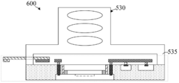
상응하게, 본 발명의 실시예는 렌즈 모듈을 더 제공한다. 도 21에 도시된 바와 같이, 본 발명에 따른 렌즈 모듈의 일 실시예의 구조 모식도를 나타낸다.Correspondingly, embodiments of the present invention further provide a lens module. As shown in FIG. 21, a structural schematic diagram of one embodiment of a lens module according to the present invention is shown.
상기 렌즈 모듈(600)은 본 발명의 실시예에 따른 촬영 어셈블리(도 21 중 점선 블록에 도시된 바와 같음)를 포함한다. 렌즈 어셈블리(530)는 홀더(535)를 포함하고, 상기 홀더(535)는 상기 패키징층(미도시)의 최상면에 장착되며 상기 감광성 유닛(미도시) 및 기능 소자(미도시)를 둘러싸고, 상기 렌즈 어셈블리(530)는 상기 감광성 칩(미도시) 및 기능 소자와 전기적으로 연결된다.The
상기 렌즈 어셈블리(530)는 일반적으로 홀더(535), 상기 홀더(535)에 장착되는 모터(미도시), 및 상기 모터에 장착되는 렌즈 시스템(미도시)을 포함하고, 상기 홀더(535)를 통해 상기 렌즈 어셈블리(530)를 용이하게 조립하고, 렌즈 시스템이 감광성 유닛의 감광성 경로에 위치하도록 한다.The
본 실시예에서, 상기 촬영 어셈블리의 두께는 비교적 작고, 상기 패키징층을 통해 상기 렌즈 어셈블리(530)의 두께를 감소시킴으로써, 상기 렌즈 모듈(600)의 전체 두께를 감소시킨다.In this embodiment, the thickness of the photographing assembly is relatively small, and by reducing the thickness of the
또한, 상기 감광성 유닛 및 기능 소자(예를 들어, 주변 칩)를 모두 상기 홀더(535) 내부에 설치하는 해결수단과 기능 소자를 주변 메인보드에 장착하는 해결수단을 비교해보면, 본 실시예는 렌즈 모듈(600)의 사이즈를 감소시키고, 전기적 연결의 거리를 단축시키므로, 렌즈 모듈(600)의 신호 전송 속도를 향상시키고, 렌즈 모듈(600)의 사용 성능을 향상시킨다(예를 들어, 촬영 속도 및 저장 속도를 향상시킴).In addition, comparing the solution for installing the photosensitive unit and the functional element (for example, a peripheral chip) inside the
또한, 상기 감광성 유닛 및 기능 소자를 모두 패키징층 내에 집적시키고 상기 감광성 유닛, 기능 소자 및 재배선 구조를 모두 상기 홀더(535) 내부에 설치하여, 상기 감광성 유닛, 기능 소자 및 재배선 구조를 모두 보호하므로, 상기 렌즈 모듈(600)의 신뢰성과 안정성을 향상시키는데 유리하고, 상기 렌즈 모듈(600)의 이미징 품질을 보장할 수 있다.In addition, all the photosensitive units and functional elements are integrated in a packaging layer, and all the photosensitive units, functional elements, and redistribution structures are installed inside the
본 실시예에서, 상기 재배선 구조에 연성회로기판(FPC)이 본딩되므로, 상기 렌즈 어셈블리(530) 중의 모터는 상응하게 연성회로기판(FPC)을 통해 촬영 어셈블리 중의 각 칩 및 소자와 전기적으로 연결된다.In this embodiment, since a flexible circuit board (FPC) is bonded to the redistribution structure, a motor in the
본 실시예에 따른 촬영 어셈블리의 구체적인 설명은 전술한 실시예에서의 상응한 설명을 참조할 수 있고, 여기서 더 설명하지 않도록 한다.For a detailed description of the imaging assembly according to the present embodiment, reference may be made to the corresponding description in the above-described embodiment, and will not be described further herein.
상응하게, 본 발명의 실시예는 전자 기기를 더 제공한다. 도 22를 참조하면, 본 발명에 따른 전자 기기의 일 실시예의 구조 모식도를 나타낸다.Correspondingly, embodiments of the present invention further provide electronic devices. 22, a structural schematic diagram of an embodiment of an electronic device according to the present invention is shown.
본 실시예에서, 상기 전자 기기(700)는 본 발명의 실시예에 따른 렌즈 모듈(600)을 포함한다.In this embodiment, the
상기 렌즈 모듈(600)의 신뢰성과 성능은 비교적 높기에, 상응하게 상기 전자 기기(700)의 촬영 품질, 촬영 속도 및 저장 속도를 향상시킨다. 또한, 상기 렌즈 모듈(600)의 전체 두께가 비교적 작으므로, 사용자의 사용 체험을 향상시키는데 유리하다.Since the reliability and performance of the
구체적으로, 상기 전자 기기(700)는 휴대폰, 태블릿 PC, 카메라 또는 비디오 카메라 등 각종 촬영 기능을 구비하는 기기일 수 있다.Specifically, the
본 발명은 상술한 바와 같이 개시하였지만, 본 발명은 이에 한정되지 않는다. 임의의 당업자는 본 발명의 사상과 범위를 벗어나지 않는 전제 하에 모두 여러가지 변경과 수정을 진행할 수 있으므로, 본 발명의 보호 범위는 청구범위에 한정된 범위를 기준으로 해야 한다.Although the present invention has been disclosed as described above, the present invention is not limited thereto. Any person skilled in the art can make various changes and modifications without departing from the spirit and scope of the present invention, so the protection scope of the present invention should be based on the scope defined in the claims.
Claims (27)
용접 패드를 구비하는 감광성 칩 및 필터를 제공하는 단계;
상기 감광성 칩의 용접 패드를 향하는 상기 필터를 상기 감광성 칩에 장착하는 단계;
용접 패드를 구비하는 기능 소자 및 상기 필터가 임시 본딩되는 제1 캐리어 기판을 제공하되, 상기 기능 소자의 용접 패드는 상기 제1 캐리어 기판을 향하는 단계;
상기 제1 캐리어 기판 및 기능 소자를 커버하고 상기 감광성 칩의 부분 측벽을 적어도 커버하는 패키징층을 형성하는 단계;
상기 제1 캐리어 기판을 제거하는 단계; 및
상기 제1 캐리어 기판을 제거한 후, 상기 패키징층에서의 상기 필터에 근접하는 일측에 상기 감광성 칩의 용접 패드 및 상기 기능 소자의 용접 패드에 전기적으로 연결되는 재배선 구조를 형성하는 단계를 포함하는 것을 특징으로 하는 촬영 어셈블리의 패키징 방법.As a packaging method of the shooting assembly,
Providing a photosensitive chip and a filter having a welding pad;
Mounting the filter facing the welding pad of the photosensitive chip to the photosensitive chip;
Providing a first carrier substrate to which the functional element having a welding pad and the filter are temporarily bonded, wherein the welding pad of the functional element faces the first carrier substrate;
Forming a packaging layer covering the first carrier substrate and the functional element and covering at least a partial sidewall of the photosensitive chip;
Removing the first carrier substrate; And
After removing the first carrier substrate, forming a redistribution structure electrically connected to a welding pad of the photosensitive chip and a welding pad of the functional element on one side proximate to the filter in the packaging layer. Packaging method of the shooting assembly characterized by.
상기 재배선 구조를 형성하는 단계는,
상기 패키징층 내에 상기 감광성 칩의 용접 패드에 전기적으로 연결되는 전도성 칼럼을 형성하는 단계; 및
상기 패키징층에서의 상기 필터에 근접하는 일측에 상기 전도성 칼럼 및 기능 소자의 용접 패드에 전기적으로 연결되는 연결선을 형성하는 단계를 포함하는 것을 특징으로 하는 촬영 어셈블리의 패키징 방법.According to claim 1,
The step of forming the redistribution structure,
Forming a conductive column electrically connected to a welding pad of the photosensitive chip in the packaging layer; And
And forming a connection line electrically connected to the conductive column and the welding pad of the functional element on one side proximate to the filter in the packaging layer.
상기 전도성 칼럼을 형성하는 단계는,
상기 패키징층을 패턴화하여 상기 패키징층 내에 상기 감광성 칩의 용접 패드를 노출시키는 전도성 관통홀을 형성하는 단계; 및
상기 전도성 관통홀 내에 상기 전도성 칼럼을 형성하는 단계를 포함하는 것을 특징으로 하는 촬영 어셈블리의 패키징 방법.According to claim 2,
The step of forming the conductive column,
Patterning the packaging layer to form a conductive through-hole exposing the welding pad of the photosensitive chip in the packaging layer; And
And forming the conductive column in the conductive through-hole.
상기 연결선을 형성하는 단계는,
상기 연결선이 형성되는 제2 캐리어 기판을 제공하는 단계를 포함하고,
상기 재배선 구조를 형성하는 단계는,
상기 전도성 칼럼 및 기능 소자의 용접 패드에 전도성 돌출 블록을 형성하는 단계; 및
상기 연결선을 상기 전도성 돌출 블록에 본딩시키는 단계를 더 포함하는 것을 특징으로 하는 촬영 어셈블리의 패키징 방법.According to claim 2,
The step of forming the connecting line,
And providing a second carrier substrate on which the connection line is formed.
The step of forming the redistribution structure,
Forming a conductive protruding block on the conductive column and the welding pad of the functional element; And
And bonding the connecting line to the conductive protruding block.
상기 연결선을 형성하는 단계는,
상기 연결선이 형성되는 제2 캐리어 기판을 형성하는 단계를 포함하고,
상기 재배선 구조를 형성하는 단계는,
상기 연결선에 전도성 돌출 블록을 형성하는 단계; 및
상기 전도성 돌출 블록을 대응되는 상기 전도성 칼럼 및 기능 소자의 용접 패드에 본딩시키는 단계를 더 포함하는 것을 특징으로 하는 촬영 어셈블리의 패키징 방법.According to claim 2,
The step of forming the connecting line,
And forming a second carrier substrate on which the connection line is formed,
The step of forming the redistribution structure,
Forming a conductive protrusion block on the connection line; And
And bonding the conductive protruding block to the corresponding conductive column and welding pads of the functional element.
상기 제2 캐리어 기판에 상기 연결선을 형성하는 단계는,
상기 제2 캐리어 기판에 제1 매질층을 형성하는 단계;
상기 제1 매질층을 패턴화하여 상기 제1 매질층 내에 제1 연결홈을 형성하는 단계;
상기 제1 연결홈 내에 상기 연결선을 형성하는 단계; 및
상기 제1 매질층을 제거하는 단계를 포함하는 것을 특징으로 하는 촬영 어셈블리의 패키징 방법.The method of claim 4 or 5,
Forming the connection line on the second carrier substrate,
Forming a first medium layer on the second carrier substrate;
Patterning the first medium layer to form a first connection groove in the first medium layer;
Forming the connection line in the first connection groove; And
And removing the first medium layer.
상기 연결선에 전도성 돌출 블록을 형성하는 단계는,
상기 제2 캐리어 기판 및 연결선을 커버하는 제2 매질층을 형성하는 단계;
상기 제2 매질층을 패턴화하여 상기 제2 매질층 내에 연결 관통홀을 형성하고 상기 연결선의 일부분을 노출시키는 단계;
상기 연결 관통홀 내에 상기 전도성 돌출 블록을 형성하는 단계; 및
상기 제2 매질층을 제거하는 단계를 포함하는 것을 특징으로 하는 촬영 어셈블리의 패키징 방법.The method of claim 5,
Forming a conductive protrusion block on the connecting line,
Forming a second medium layer covering the second carrier substrate and the connection line;
Patterning the second medium layer to form a connection through hole in the second medium layer and exposing a portion of the connection line;
Forming the conductive protrusion block in the connection through hole; And
And removing the second medium layer.
상기 연결선을 형성하는 단계는,
상기 전도성 관통홀을 형성한 후, 상기 패키징층 및 필터를 커버하는, 상기 전도성 관통홀 내에 위치하는 제3 매질층을 형성하는 단계;
상기 제3 매질층을 패턴화하여 상기 전도성 관통홀 내에 위치하고 상기 패키징층 최상부의 부분 영역보다 높은 제3 매질층을 제거하고, 상기 제3 매질층 내에 제2 연결홈을 형성하며, 상기 기능 소자의 용접 패드를 노출시키고, 상기 제2 연결홈과 상기 전도성 관통홀을 전기적으로 연결시키는 단계;
상기 전도성 관통홀 내에 상기 전도성 칼럼을 형성하는 단계에서, 상기 제2 연결홈 내에 상기 연결선을 형성하는 단계; 및
상기 제3 매질층을 제거하는 단계를 포함하는 것을 특징으로 하는 촬영 어셈블리의 패키징 방법.According to claim 3,
The step of forming the connecting line,
After forming the conductive through hole, forming a third medium layer located in the conductive through hole, covering the packaging layer and the filter;
The third medium layer is patterned to remove a third medium layer located in the conductive through-hole and higher than a partial region on the top of the packaging layer, to form a second connection groove in the third medium layer, Exposing a welding pad and electrically connecting the second connection groove and the conductive through hole;
In the step of forming the conductive column in the conductive through-hole, forming the connecting line in the second connection groove; And
And removing the third medium layer.
레이저 식각 공정을 통해 상기 패키징층을 패턴화하는 것을 특징으로 하는 촬영 어셈블리의 패키징 방법.According to claim 3,
The packaging method of the imaging assembly, characterized in that the patterning of the packaging layer through a laser etching process.
전기도금 공정을 이용하여 상기 전도성 관통홀 내에 상기 전도성 칼럼을 형성하는 것을 특징으로 하는 촬영 어셈블리의 패키징 방법.According to claim 3,
Packaging method of the imaging assembly, characterized in that the conductive column is formed in the conductive through-hole using an electroplating process.
범핑(bumping) 공정을 이용하여 상기 전도성 돌출 블록을 형성하는 것을 특징으로 하는 촬영 어셈블리의 패키징 방법.The method of claim 4,
Packaging method of the shooting assembly, characterized in that to form the conductive protrusion block using a bumping (bumping) process.
전기도금 공정을 이용하여 상기 전도성 관통홀 내에 상기 전도성 칼럼을 형성하고 상기 제2 연결홈 내에 상기 연결선을 형성하는 것을 특징으로 하는 촬영 어셈블리의 패키징 방법.The method of claim 8,
Packaging method of the shooting assembly, characterized in that by forming the conductive column in the conductive through-hole using the electroplating process and forming the connecting line in the second connecting groove.
금속 본딩 공정을 이용하여 본딩 단계를 진행하는 것을 특징으로 하는 촬영 어셈블리의 패키징 방법.The method of claim 4 or 5,
Packaging method of the shooting assembly, characterized in that the bonding step using a metal bonding process.
상기 필터를 상기 감광성 칩에 장착한 후, 상기 제1 캐리어 기판에 상기 필터를 임시 본딩시키거나; 또는
상기 제1 캐리어 기판에 상기 필터를 임시 본딩시킨 후, 상기 필터를 상기 감광성 칩에 장착하는 것을 특징으로 하는 촬영 어셈블리의 패키징 방법.According to claim 1,
After mounting the filter on the photosensitive chip, temporarily bonding the filter to the first carrier substrate; or
After the temporary bonding of the filter to the first carrier substrate, the method of packaging the imaging assembly, characterized in that mounting the filter to the photosensitive chip.
상기 패키징층을 형성하는 단계 이전에,
상기 필터의 측벽을 커버하는 응력 완충층을 형성하는 단계를 더 포함하는 것을 특징으로 하는 촬영 어셈블리의 패키징 방법.According to claim 1,
Before the step of forming the packaging layer,
And forming a stress buffer layer covering the sidewalls of the filter.
상기 패키징층을 형성하는 단계는,
상기 제1 캐리어 기판, 기능 소자 및 감광성 칩을 커버하는 패키징 재료층을 형성하는 단계; 및
상기 패키징 재료층에 대해 연삭(grinding) 처리를 진행하여 상기 감광성 유닛 및 기능 소자 높은 것과 서로 평행되는 상기 패키징층을 형성하는 단계를 포함하는 것을 특징으로 하는 촬영 어셈블리의 패키징 방법.According to claim 1,
The step of forming the packaging layer,
Forming a layer of packaging material covering the first carrier substrate, functional element and photosensitive chip; And
And a step of grinding the packaging material layer to form the packaging layer parallel to the photosensitive unit and the functional element high.
상기 패키징층에서의 상기 필터에 근접하는 일측에 재배선 구조를 형성하는 단계 이후에, 상기 재배선 구조에 연성회로기판(FPC)을 본딩시키는 단계를 더 포함하는 것을 특징으로 하는 촬영 어셈블리의 패키징 방법.According to claim 1,
After the step of forming a redistribution structure on one side of the packaging layer close to the filter, bonding the flexible circuit board (FPC) to the redistribution structure further comprises a method for packaging an imaging assembly. .
상기 금속 본딩 공정의 공정 온도는 250 ℃보다 작거나 같고, 공정 압력은 200 kPa보다 크거나 같으며, 공정 시간은 30 분보다 크거나 같은 것을 특징으로 하는 촬영 어셈블리의 패키징 방법.The method of claim 13,
The metal bonding process has a process temperature of less than or equal to 250°C, a process pressure of greater than or equal to 200 kPa, and a process time of greater than or equal to 30 minutes.
패키징층, 상기 패키징층에 삽입되는 감광성 유닛, 기능 소자 및 재배선 구조를 포함하되,
상기 감광성 유닛은 감광성 칩 및 상기 감광성 칩에 장착되는 필터를 포함하고, 상기 패키징층의 최상면은 상기 필터 및 기능 소자를 노출시키며, 상기 패키징층의 저면은 상기 기능 소자보다 높고, 상기 패키징층은 상기 감광성 칩의 부분 측벽을 적어도 커버하며, 상기 감광성 칩 및 기능 소자는 모두 용접 패드를 구비하고, 상기 감광성 칩의 용접 패드는 상기 패키징층의 최상면을 향하며, 상기 기능 소자의 용접 패드는 상기 패키징층의 최상면에 노출되고,
상기 재배선 구조는 상기 패키징층에서의 상기 필터에 근접하는 일측에 위치하고, 상기 재배선 구조는 상기 용접 패드에 전기적으로 연결되는 것을 특징으로 하는 촬영 어셈블리.As a shooting assembly,
It includes a packaging layer, a photosensitive unit inserted into the packaging layer, a functional element and a redistribution structure,
The photosensitive unit includes a photosensitive chip and a filter mounted on the photosensitive chip, the top surface of the packaging layer exposes the filter and functional element, the bottom surface of the packaging layer is higher than the functional element, and the packaging layer is the At least a partial sidewall of the photosensitive chip, the photosensitive chip and the functional element are both equipped with a welding pad, the welding pad of the photosensitive chip faces the uppermost surface of the packaging layer, and the welding pad of the functional element is the packaging layer Exposed on the top surface,
The redistribution structure is located on one side close to the filter in the packaging layer, and the redistribution structure is an imaging assembly, characterized in that electrically connected to the welding pad.
상기 재배선 구조는,
상기 패키징층 내에 위치하고 상기 감광성 칩의 용접 패드에 전기적으로 연결되는 전도성 칼럼; 및
상기 기능 소자의 용접 패드 및 상기 전도성 칼럼에 위치하고, 상기 기능 소자의 용접 패드 및 상기 전도성 칼럼에 전기적으로 연결되는 연결선을 포함하는 것을 특징으로 하는 촬영 어셈블리.The method of claim 19,
The redistribution structure,
A conductive column located in the packaging layer and electrically connected to a welding pad of the photosensitive chip; And
And a connecting line located on the welding pad and the conductive column of the functional element, and electrically connected to the welding pad and the conductive column of the functional element.
상기 재배선 구조는, 상기 연결선과 상기 기능 소자의 용접 패드 및 전도성 칼럼 사이에 각각 위치하는 전도성 돌출 블록을 더 포함하는 것을 특징으로 하는 촬영 어셈블리.The method of claim 20,
The redistribution structure further comprises a conductive protruding block positioned between the connection line and the welding pad and the conductive column of the functional element, respectively.
상기 패키징층의 저면은 상기 감광성 유닛 및 기능 소자 중 높은 것과 서로 평행되는 것을 특징으로 하는 촬영 어셈블리.The method of claim 19,
The photographing assembly, characterized in that the bottom surface of the packaging layer is parallel to each other high of the photosensitive unit and functional elements.
상기 촬영 어셈블리는 상기 필터의 측벽과 상기 패키징층 사이에 위치하는 응력 완충층을 더 포함하는 것을 특징으로 하는 촬영 어셈블리.The method of claim 19,
The imaging assembly further comprises a stress buffer layer positioned between the sidewall of the filter and the packaging layer.
상기 기능 소자는 주변 칩 및 수동 소자 중 적어도 한 가지를 포함하고, 상기 주변 칩은 디지털 신호 프로세서 칩 및 메모리 칩 중 한 가지 또는 두 가지를 포함하는 것을 특징으로 하는 촬영 어셈블리.The method of claim 19,
The functional element includes at least one of a peripheral chip and a passive element, and the peripheral chip includes one or two of a digital signal processor chip and a memory chip.
상기 촬영 어셈블리는 상기 재배선 구조에 위치하는 연성회로기판(FPC)을 더 포함하는 것을 특징으로 하는 촬영 어셈블리.The method of claim 19,
The imaging assembly further comprises a flexible circuit board (FPC) positioned in the redistribution structure.
제19항 내지 제25항 중 어느 한 항에 따른 촬영 어셈블리; 및
상기 패키징층의 최상면에 장착되고 상기 감광성 유닛 및 기능 소자를 둘러싸는 홀더를 포함하고 상기 감광성 칩 및 기능 소자에 전기적으로 연결되는 렌즈 어셈블리를 포함하는 것을 특징으로 하는 렌즈 모듈.As a lens module,
A photographing assembly according to any one of claims 19 to 25; And
And a lens assembly mounted on an uppermost surface of the packaging layer and surrounding the photosensitive unit and the functional element, and a lens assembly electrically connected to the photosensitive chip and the functional element.
An electronic device comprising the lens module according to claim 26.
Applications Claiming Priority (3)
| Application Number | Priority Date | Filing Date | Title |
|---|---|---|---|
| CN201811385636.7A CN111199984B (en) | 2018-11-20 | 2018-11-20 | Camera shooting assembly and packaging method thereof, lens module and electronic equipment |
| CN201811385636.7 | 2018-11-20 | ||
| PCT/CN2018/119987 WO2020103214A1 (en) | 2018-11-20 | 2018-12-10 | Camera assembly and packaging method therefor, lens module, and electronic device |
Publications (2)
| Publication Number | Publication Date |
|---|---|
| KR20200063102A true KR20200063102A (en) | 2020-06-04 |
| KR102249873B1 KR102249873B1 (en) | 2021-05-12 |
Family
ID=70746953
Family Applications (1)
| Application Number | Title | Priority Date | Filing Date |
|---|---|---|---|
| KR1020197036797A KR102249873B1 (en) | 2018-11-20 | 2018-12-10 | Photographic assembly and packaging method thereof, lens module, electronic device |
Country Status (4)
| Country | Link |
|---|---|
| JP (1) | JP6993726B2 (en) |
| KR (1) | KR102249873B1 (en) |
| CN (1) | CN111199984B (en) |
| WO (1) | WO2020103214A1 (en) |
Cited By (3)
| Publication number | Priority date | Publication date | Assignee | Title |
|---|---|---|---|---|
| KR20220034437A (en) * | 2020-09-11 | 2022-03-18 | 주식회사 옵트론텍 | Optical filter carrier, image sensor package having optical filter, and method of fabricating the same |
| WO2023282490A1 (en) * | 2021-07-06 | 2023-01-12 | 삼성전자 주식회사 | Electronic device comprising camera module |
| WO2023043254A1 (en) * | 2021-09-16 | 2023-03-23 | 엘지이노텍 주식회사 | Camera module and optical device comprising same |
Families Citing this family (3)
| Publication number | Priority date | Publication date | Assignee | Title |
|---|---|---|---|---|
| TWI780979B (en) * | 2021-11-10 | 2022-10-11 | 力晶積成電子製造股份有限公司 | Method for manufacturing fingerprint sensing module |
| CN114220826A (en) * | 2021-12-14 | 2022-03-22 | 上海集成电路装备材料产业创新中心有限公司 | Chip packaging structure and chip packaging method |
| CN117692732A (en) * | 2022-08-24 | 2024-03-12 | 宏启胜精密电子(秦皇岛)有限公司 | Imaging module and preparation method thereof |
Citations (6)
| Publication number | Priority date | Publication date | Assignee | Title |
|---|---|---|---|---|
| JP2000235989A (en) * | 1999-02-16 | 2000-08-29 | Furukawa Electric Co Ltd:The | Manufacture of circuit board with bump |
| JP2002170921A (en) * | 2000-12-01 | 2002-06-14 | Matsushita Electric Ind Co Ltd | Semiconductor device and its manufacturing method |
| JP2005223183A (en) * | 2004-02-06 | 2005-08-18 | Matsushita Electric Ind Co Ltd | Electronic component mounted board and method for manufacturing the same |
| JP2006005612A (en) * | 2004-06-17 | 2006-01-05 | Shinko Electric Ind Co Ltd | Imaging module |
| JP2008277569A (en) * | 2007-04-27 | 2008-11-13 | Oki Electric Ind Co Ltd | Semiconductor device and manufacturing method therefor |
| JP2009176894A (en) * | 2008-01-23 | 2009-08-06 | Panasonic Corp | Optical semiconductor device |
Family Cites Families (13)
| Publication number | Priority date | Publication date | Assignee | Title |
|---|---|---|---|---|
| JP4497304B2 (en) * | 2004-11-22 | 2010-07-07 | エルピーダメモリ株式会社 | Semiconductor device and manufacturing method thereof |
| JP4382030B2 (en) * | 2005-11-15 | 2009-12-09 | 富士通マイクロエレクトロニクス株式会社 | Semiconductor device and manufacturing method thereof |
| CN101419921A (en) * | 2007-10-24 | 2009-04-29 | 中芯国际集成电路制造(上海)有限公司 | Chip dimension encapsulation method for image sensor |
| JP2013528318A (en) * | 2010-06-11 | 2013-07-08 | 日本電気株式会社 | Rewiring method of functional elements |
| US8890269B2 (en) * | 2012-05-31 | 2014-11-18 | Stmicroelectronics Pte Ltd. | Optical sensor package with through vias |
| US9059058B2 (en) * | 2012-10-22 | 2015-06-16 | Stmicroelectronics Pte Ltd | Image sensor device with IR filter and related methods |
| CN104465575B (en) * | 2013-09-17 | 2019-04-12 | 日月光半导体制造股份有限公司 | Semiconductor packages and its manufacturing method |
| TWI608244B (en) * | 2015-08-07 | 2017-12-11 | 佳能股份有限公司 | Photoelectric conversion device, ranging apparatus, and information processing system |
| CN206042171U (en) * | 2016-10-08 | 2017-03-22 | 杭州海康威视数字技术股份有限公司 | Beam split mechanism and mount pad thereof |
| US10644046B2 (en) * | 2017-04-07 | 2020-05-05 | Samsung Electronics Co., Ltd. | Fan-out sensor package and optical fingerprint sensor module including the same |
| CN107343128A (en) * | 2017-08-16 | 2017-11-10 | 信利光电股份有限公司 | More the lens camera modules and electronic equipment of a kind of shared sensitive chip |
| CN207053633U (en) * | 2017-08-16 | 2018-02-27 | 信利光电股份有限公司 | A kind of camera module and camera device |
| CN107507821A (en) * | 2017-09-05 | 2017-12-22 | 中芯长电半导体(江阴)有限公司 | The encapsulating structure and method for packing of integrated image sensor chip and logic chip |
-
2018
- 2018-11-20 CN CN201811385636.7A patent/CN111199984B/en active Active
- 2018-12-10 WO PCT/CN2018/119987 patent/WO2020103214A1/en active Application Filing
- 2018-12-10 KR KR1020197036797A patent/KR102249873B1/en active IP Right Grant
- 2018-12-10 JP JP2019568373A patent/JP6993726B2/en active Active
Patent Citations (6)
| Publication number | Priority date | Publication date | Assignee | Title |
|---|---|---|---|---|
| JP2000235989A (en) * | 1999-02-16 | 2000-08-29 | Furukawa Electric Co Ltd:The | Manufacture of circuit board with bump |
| JP2002170921A (en) * | 2000-12-01 | 2002-06-14 | Matsushita Electric Ind Co Ltd | Semiconductor device and its manufacturing method |
| JP2005223183A (en) * | 2004-02-06 | 2005-08-18 | Matsushita Electric Ind Co Ltd | Electronic component mounted board and method for manufacturing the same |
| JP2006005612A (en) * | 2004-06-17 | 2006-01-05 | Shinko Electric Ind Co Ltd | Imaging module |
| JP2008277569A (en) * | 2007-04-27 | 2008-11-13 | Oki Electric Ind Co Ltd | Semiconductor device and manufacturing method therefor |
| JP2009176894A (en) * | 2008-01-23 | 2009-08-06 | Panasonic Corp | Optical semiconductor device |
Cited By (3)
| Publication number | Priority date | Publication date | Assignee | Title |
|---|---|---|---|---|
| KR20220034437A (en) * | 2020-09-11 | 2022-03-18 | 주식회사 옵트론텍 | Optical filter carrier, image sensor package having optical filter, and method of fabricating the same |
| WO2023282490A1 (en) * | 2021-07-06 | 2023-01-12 | 삼성전자 주식회사 | Electronic device comprising camera module |
| WO2023043254A1 (en) * | 2021-09-16 | 2023-03-23 | 엘지이노텍 주식회사 | Camera module and optical device comprising same |
Also Published As
| Publication number | Publication date |
|---|---|
| CN111199984B (en) | 2022-12-02 |
| CN111199984A (en) | 2020-05-26 |
| WO2020103214A1 (en) | 2020-05-28 |
| JP2021511654A (en) | 2021-05-06 |
| JP6993726B2 (en) | 2022-01-14 |
| KR102249873B1 (en) | 2021-05-12 |
Similar Documents
| Publication | Publication Date | Title |
|---|---|---|
| KR102249873B1 (en) | Photographic assembly and packaging method thereof, lens module, electronic device | |
| CN109274876B (en) | Photosensitive assembly and packaging method thereof, lens module and electronic equipment | |
| KR102249883B1 (en) | Photographic assembly and packaging method thereof, lens module, electronic device | |
| US20210320095A1 (en) | Camera assembly, lens module, and electronic device | |
| US11430825B2 (en) | Image capturing assembly, lens module and electronic device | |
| US20220045112A1 (en) | Camera assembly, lens module, and electronic device | |
| US20200161356A1 (en) | Camera assembly and packaging method, lens module and electronic device | |
| US11296141B2 (en) | Image capturing assembly and packaging method thereof, lens module, and electronic device | |
| KR102333741B1 (en) | Photography assembly and packaging method thereof, lens module, electronic device | |
| US11171166B2 (en) | Camera assembly and packaging method thereof, lens module, electronic device | |
| CN111263028B (en) | Camera shooting assembly and packaging method thereof, lens module and electronic equipment | |
| KR102250603B1 (en) | Photographic assembly and packaging method thereof, lens module, electronic device | |
| US20090315130A1 (en) | Solid-state imaging apparatus and method for manufacturing the same |
Legal Events
| Date | Code | Title | Description |
|---|---|---|---|
| E902 | Notification of reason for refusal | ||
| E701 | Decision to grant or registration of patent right | ||
| GRNT | Written decision to grant |