KR20200044992A - How to create independent membranes for biological applications - Google Patents
How to create independent membranes for biological applications Download PDFInfo
- Publication number
- KR20200044992A KR20200044992A KR1020207011448A KR20207011448A KR20200044992A KR 20200044992 A KR20200044992 A KR 20200044992A KR 1020207011448 A KR1020207011448 A KR 1020207011448A KR 20207011448 A KR20207011448 A KR 20207011448A KR 20200044992 A KR20200044992 A KR 20200044992A
- Authority
- KR
- South Korea
- Prior art keywords
- substrate
- nanopores
- thin film
- forming
- layer
- Prior art date
Links
Images


Classifications
-
- H—ELECTRICITY
- H01—ELECTRIC ELEMENTS
- H01L—SEMICONDUCTOR DEVICES NOT COVERED BY CLASS H10
- H01L21/00—Processes or apparatus adapted for the manufacture or treatment of semiconductor or solid state devices or of parts thereof
- H01L21/70—Manufacture or treatment of devices consisting of a plurality of solid state components formed in or on a common substrate or of parts thereof; Manufacture of integrated circuit devices or of parts thereof
- H01L21/71—Manufacture of specific parts of devices defined in group H01L21/70
- H01L21/768—Applying interconnections to be used for carrying current between separate components within a device comprising conductors and dielectrics
- H01L21/76801—Applying interconnections to be used for carrying current between separate components within a device comprising conductors and dielectrics characterised by the formation and the after-treatment of the dielectrics, e.g. smoothing
- H01L21/76802—Applying interconnections to be used for carrying current between separate components within a device comprising conductors and dielectrics characterised by the formation and the after-treatment of the dielectrics, e.g. smoothing by forming openings in dielectrics
- H01L21/76816—Aspects relating to the layout of the pattern or to the size of vias or trenches
-
- G—PHYSICS
- G01—MEASURING; TESTING
- G01N—INVESTIGATING OR ANALYSING MATERIALS BY DETERMINING THEIR CHEMICAL OR PHYSICAL PROPERTIES
- G01N33/00—Investigating or analysing materials by specific methods not covered by groups G01N1/00 - G01N31/00
- G01N33/48—Biological material, e.g. blood, urine; Haemocytometers
- G01N33/483—Physical analysis of biological material
- G01N33/487—Physical analysis of biological material of liquid biological material
- G01N33/48707—Physical analysis of biological material of liquid biological material by electrical means
- G01N33/48721—Investigating individual macromolecules, e.g. by translocation through nanopores
-
- B—PERFORMING OPERATIONS; TRANSPORTING
- B81—MICROSTRUCTURAL TECHNOLOGY
- B81C—PROCESSES OR APPARATUS SPECIALLY ADAPTED FOR THE MANUFACTURE OR TREATMENT OF MICROSTRUCTURAL DEVICES OR SYSTEMS
- B81C1/00—Manufacture or treatment of devices or systems in or on a substrate
- B81C1/00015—Manufacture or treatment of devices or systems in or on a substrate for manufacturing microsystems
- B81C1/00023—Manufacture or treatment of devices or systems in or on a substrate for manufacturing microsystems without movable or flexible elements
- B81C1/00087—Holes
-
- B—PERFORMING OPERATIONS; TRANSPORTING
- B81—MICROSTRUCTURAL TECHNOLOGY
- B81C—PROCESSES OR APPARATUS SPECIALLY ADAPTED FOR THE MANUFACTURE OR TREATMENT OF MICROSTRUCTURAL DEVICES OR SYSTEMS
- B81C1/00—Manufacture or treatment of devices or systems in or on a substrate
- B81C1/00015—Manufacture or treatment of devices or systems in or on a substrate for manufacturing microsystems
- B81C1/00134—Manufacture or treatment of devices or systems in or on a substrate for manufacturing microsystems comprising flexible or deformable structures
- B81C1/00158—Diaphragms, membranes
-
- B—PERFORMING OPERATIONS; TRANSPORTING
- B82—NANOTECHNOLOGY
- B82B—NANOSTRUCTURES FORMED BY MANIPULATION OF INDIVIDUAL ATOMS, MOLECULES, OR LIMITED COLLECTIONS OF ATOMS OR MOLECULES AS DISCRETE UNITS; MANUFACTURE OR TREATMENT THEREOF
- B82B1/00—Nanostructures formed by manipulation of individual atoms or molecules, or limited collections of atoms or molecules as discrete units
- B82B1/002—Devices comprising flexible or deformable elements
-
- B—PERFORMING OPERATIONS; TRANSPORTING
- B82—NANOTECHNOLOGY
- B82B—NANOSTRUCTURES FORMED BY MANIPULATION OF INDIVIDUAL ATOMS, MOLECULES, OR LIMITED COLLECTIONS OF ATOMS OR MOLECULES AS DISCRETE UNITS; MANUFACTURE OR TREATMENT THEREOF
- B82B3/00—Manufacture or treatment of nanostructures by manipulation of individual atoms or molecules, or limited collections of atoms or molecules as discrete units
- B82B3/0009—Forming specific nanostructures
- B82B3/0023—Forming specific nanostructures comprising flexible or deformable elements
-
- G—PHYSICS
- G01—MEASURING; TESTING
- G01N—INVESTIGATING OR ANALYSING MATERIALS BY DETERMINING THEIR CHEMICAL OR PHYSICAL PROPERTIES
- G01N27/00—Investigating or analysing materials by the use of electric, electrochemical, or magnetic means
- G01N27/26—Investigating or analysing materials by the use of electric, electrochemical, or magnetic means by investigating electrochemical variables; by using electrolysis or electrophoresis
- G01N27/416—Systems
- G01N27/447—Systems using electrophoresis
- G01N27/44756—Apparatus specially adapted therefor
- G01N27/44791—Microapparatus
-
- H—ELECTRICITY
- H01—ELECTRIC ELEMENTS
- H01L—SEMICONDUCTOR DEVICES NOT COVERED BY CLASS H10
- H01L21/00—Processes or apparatus adapted for the manufacture or treatment of semiconductor or solid state devices or of parts thereof
- H01L21/02—Manufacture or treatment of semiconductor devices or of parts thereof
- H01L21/02104—Forming layers
- H01L21/02107—Forming insulating materials on a substrate
- H01L21/02225—Forming insulating materials on a substrate characterised by the process for the formation of the insulating layer
- H01L21/0226—Forming insulating materials on a substrate characterised by the process for the formation of the insulating layer formation by a deposition process
-
- H—ELECTRICITY
- H01—ELECTRIC ELEMENTS
- H01L—SEMICONDUCTOR DEVICES NOT COVERED BY CLASS H10
- H01L21/00—Processes or apparatus adapted for the manufacture or treatment of semiconductor or solid state devices or of parts thereof
- H01L21/02—Manufacture or treatment of semiconductor devices or of parts thereof
- H01L21/04—Manufacture or treatment of semiconductor devices or of parts thereof the devices having at least one potential-jump barrier or surface barrier, e.g. PN junction, depletion layer or carrier concentration layer
- H01L21/18—Manufacture or treatment of semiconductor devices or of parts thereof the devices having at least one potential-jump barrier or surface barrier, e.g. PN junction, depletion layer or carrier concentration layer the devices having semiconductor bodies comprising elements of Group IV of the Periodic System or AIIIBV compounds with or without impurities, e.g. doping materials
- H01L21/30—Treatment of semiconductor bodies using processes or apparatus not provided for in groups H01L21/20 - H01L21/26
- H01L21/31—Treatment of semiconductor bodies using processes or apparatus not provided for in groups H01L21/20 - H01L21/26 to form insulating layers thereon, e.g. for masking or by using photolithographic techniques; After treatment of these layers; Selection of materials for these layers
- H01L21/3105—After-treatment
- H01L21/311—Etching the insulating layers by chemical or physical means
-
- H—ELECTRICITY
- H01—ELECTRIC ELEMENTS
- H01L—SEMICONDUCTOR DEVICES NOT COVERED BY CLASS H10
- H01L21/00—Processes or apparatus adapted for the manufacture or treatment of semiconductor or solid state devices or of parts thereof
- H01L21/02—Manufacture or treatment of semiconductor devices or of parts thereof
- H01L21/04—Manufacture or treatment of semiconductor devices or of parts thereof the devices having at least one potential-jump barrier or surface barrier, e.g. PN junction, depletion layer or carrier concentration layer
- H01L21/18—Manufacture or treatment of semiconductor devices or of parts thereof the devices having at least one potential-jump barrier or surface barrier, e.g. PN junction, depletion layer or carrier concentration layer the devices having semiconductor bodies comprising elements of Group IV of the Periodic System or AIIIBV compounds with or without impurities, e.g. doping materials
- H01L21/30—Treatment of semiconductor bodies using processes or apparatus not provided for in groups H01L21/20 - H01L21/26
- H01L21/31—Treatment of semiconductor bodies using processes or apparatus not provided for in groups H01L21/20 - H01L21/26 to form insulating layers thereon, e.g. for masking or by using photolithographic techniques; After treatment of these layers; Selection of materials for these layers
- H01L21/3205—Deposition of non-insulating-, e.g. conductive- or resistive-, layers on insulating layers; After-treatment of these layers
- H01L21/321—After treatment
- H01L21/3213—Physical or chemical etching of the layers, e.g. to produce a patterned layer from a pre-deposited extensive layer
-
- B—PERFORMING OPERATIONS; TRANSPORTING
- B81—MICROSTRUCTURAL TECHNOLOGY
- B81B—MICROSTRUCTURAL DEVICES OR SYSTEMS, e.g. MICROMECHANICAL DEVICES
- B81B2203/00—Basic microelectromechanical structures
- B81B2203/01—Suspended structures, i.e. structures allowing a movement
- B81B2203/0127—Diaphragms, i.e. structures separating two media that can control the passage from one medium to another; Membranes, i.e. diaphragms with filtering function
-
- H—ELECTRICITY
- H01—ELECTRIC ELEMENTS
- H01L—SEMICONDUCTOR DEVICES NOT COVERED BY CLASS H10
- H01L2224/00—Indexing scheme for arrangements for connecting or disconnecting semiconductor or solid-state bodies and methods related thereto as covered by H01L24/00
- H01L2224/93—Batch processes
- H01L2224/95—Batch processes at chip-level, i.e. with connecting carried out on a plurality of singulated devices, i.e. on diced chips
- H01L2224/9512—Aligning the plurality of semiconductor or solid-state bodies
- H01L2224/95143—Passive alignment, i.e. self alignment, e.g. using surface energy, chemical reactions, thermal equilibrium
- H01L2224/95147—Passive alignment, i.e. self alignment, e.g. using surface energy, chemical reactions, thermal equilibrium by molecular lock-key, e.g. by DNA
Abstract
잘 제어된 나노포어들을 방향성 자가 조립을 사용하여 제조하는 방법들 및 독립 멤브레인들을 선택적 식각을 사용하여 제조하는 방법들이 개시된다. 일 양상에서, 이후에 박막으로 전사되는 피쳐의 임계 치수를 축소시키기 위한 블록 공중합체들을 이용한 방향성 자가 조립에 의해 하나 이상의 나노포어가 형성된다. 다른 양상에서, 방법은, 기판의 고도로 식각가능한 층 위에 박막을 갖는 기판을 제공하는 단계, 하나 이상의 나노포어를, 예를 들어, 포어 직경 감소 프로세스에 의해, 고도로 식각가능한 층 위의 박막을 통해 형성하는 단계, 및 그 다음, 얇은 독립 멤브레인을 형성하기 위해, 하나 이상의 나노포어 아래의 고도로 식각가능한 층의 부분을 선택적으로 제거하는 단계를 포함한다.Methods of manufacturing well controlled nanopores using directional self-assembly and methods of manufacturing independent membranes using selective etching are disclosed. In one aspect, one or more nanopores are formed by directional self-assembly using block copolymers to reduce the critical dimension of a feature that is subsequently transferred to a thin film. In another aspect, a method includes providing a substrate having a thin film over a highly etchable layer of a substrate, forming one or more nanopores through a thin film over a highly etchable layer, for example, by a pore diameter reduction process. And then selectively removing portions of the highly etchable layer below the one or more nanopores to form a thin independent membrane.
Description
본원에 개시된 양상들은, 잘 제어된 나노포어들을 방향성 자가 조립을 사용하여 제조하는 방법들 및 독립 멤브레인들을 선택적 식각을 사용하여 제조하는 방법들에 관한 것이다.Aspects disclosed herein relate to methods of making well-controlled nanopores using directional self-assembly and methods of making independent membranes using selective etching.
나노포어들은 데옥시리보핵산(DNA) 및 리보핵산(RNA) 서열분석과 같은 응용들에 널리 사용된다. 일 예에서, 나노포어 서열분석은, 전도성 유체에 침지된 나노포어를 통해 미지의 샘플을 운송하는 단계, 및 나노포어에 걸쳐 전위를 인가하는 단계를 일반적으로 포함하는 전기 검출 방법을 사용하여 수행된다. 나노포어를 통한 이온들의 전도로 초래되는 전류가 측정된다. 나노포어 표면에 걸친 전류 밀도의 크기는, 나노포어 치수들 및 그 때에 나노포어를 점유하고 있는 샘플, 예컨대, DNA 또는 RNA의 조성에 따른다. 상이한 뉴클레오티드들은 나노포어 표면들에 걸친 전류 밀도의 특성 변화들을 야기한다. 이러한 전류 변화들이 측정되어, DNA 또는 RNA 샘플을 서열분석하는 데에 사용된다.Nanopores are widely used in applications such as deoxyribonucleic acid (DNA) and ribonucleic acid (RNA) sequencing. In one example, nanopore sequencing is performed using an electrical detection method that generally includes transporting an unknown sample through a nanopore immersed in a conductive fluid, and applying a potential across the nanopore. . The current resulting from the conduction of ions through the nanopore is measured. The magnitude of the current density across the nanopore surface depends on the nanopore dimensions and the composition of the sample occupying the nanopore at the time, such as DNA or RNA. Different nucleotides cause characteristic changes in current density across nanopore surfaces. These current changes are measured and used to sequence DNA or RNA samples.
다양한 방법들이 생물학적 서열분석에 사용되었다. 합성에 의한 서열분석, 또는 2세대 서열분석은 어느 염기들이 DNA의 단일 가닥에 부착되었는지를 식별하는 데에 사용된다. 전체 DNA 가닥을 단일 포어에 통과시키는 것을 일반적으로 포함하는 3세대 서열분석은 DNA를 직접적으로 판독하는 데에 사용된다. 일부 서열분석 방법들은 DNA 또는 RNA 샘플이 절단되고 그 다음 재조립되는 것을 필요로 한다. 추가적으로, 일부 서열분석 방법들은 생물학적 멤브레인들 및 생물학적 포어들을 사용하는데, 이들은 저장 수명들을 가지며 사용 전에는 저온으로 유지되어야 한다.Various methods have been used for biological sequencing. Synthetic sequencing, or second generation sequencing, is used to identify which bases are attached to a single strand of DNA. Third generation sequencing, which typically involves passing the entire DNA strand through a single pore, is used to read the DNA directly. Some sequencing methods require DNA or RNA samples to be cut and then reassembled. Additionally, some sequencing methods use biological membranes and biological pores, which have shelf life and must be kept cold before use.
질화규소 또는 산화규소와 같은 독립 멤브레인 상에 형성된 나노미터 크기의 포어들인 고체 상태 나노포어들이 최근에 서열분석에 사용되었다. 그러나, 현재의 고체 상태 나노포어 제조 방법들, 예컨대, 터널링 전자 현미경, 집속 이온 빔, 또는 전자 빔을 사용하는 것은 나노포어들의 어레이들을 제조하는데 필요한 크기 및 위치 제어 요건들을 쉽고 저렴하게 달성할 수 없다. 추가적으로, 현재의 나노포어 제조 방법들은 시간 소모적이다. 게다가, 현재의 독립 멤브레인 제조 방법들은 수동이고, 시간 소모적이고, 비용이 많이 들며, DNA 또는 RNA 서열분석을 위해 최적의 얇은 두께를 갖는 독립 멤브레인을 반복적으로 형성하는 데에 효율적으로 사용될 수 없다.Solid state nanopores, nanometer-sized pores formed on independent membranes such as silicon nitride or silicon oxide, have recently been used for sequencing. However, using current solid state nanopore manufacturing methods, such as tunneling electron microscopy, focused ion beam, or electron beam, cannot easily and inexpensively achieve the size and position control requirements needed to fabricate arrays of nanopores. . Additionally, current nanopore manufacturing methods are time consuming. Moreover, current independent membrane preparation methods are manual, time consuming, costly, and cannot be efficiently used to repeatedly form independent membranes with optimal thin thicknesses for DNA or RNA sequencing.
그러므로, 관련 기술분야에서는, 생물학적 응용들을 위한, 잘 제어된 나노포어들 및 독립 멤브레인들을 제조하는 개선된 방법들이 필요하다.Therefore, there is a need in the art for improved methods of manufacturing well controlled nanopores and independent membranes for biological applications.
잘 제어된 나노포어들을 방향성 자가 조립을 사용하여 제조하는 방법들 및 독립 멤브레인들을 선택적 식각을 사용하여 제조하는 방법들이 개시된다. 일 양상에서, 이후에 박막으로 전사되는 피쳐의 임계 치수를 축소시키기 위한 블록 공중합체들을 이용한 방향성 자가 조립에 의해 하나 이상의 나노포어가 형성된다. 다른 양상에서, 방법은, 기판의 고도로 식각가능한 층 위에 박막을 갖는 기판을 제공하는 단계, 하나 이상의 나노포어를, 예를 들어, 포어 직경 감소 프로세스에 의해, 고도로 식각가능한 층 위의 박막을 통해 형성하는 단계, 및 그 다음, 얇은 독립 멤브레인을 형성하기 위해, 하나 이상의 나노포어 아래의 고도로 식각가능한 층의 부분을 선택적으로 제거하는 단계를 포함한다.Methods of manufacturing well controlled nanopores using directional self-assembly and methods of manufacturing independent membranes using selective etching are disclosed. In one aspect, one or more nanopores are formed by directional self-assembly using block copolymers to reduce the critical dimension of a feature that is subsequently transferred to a thin film. In another aspect, a method includes providing a substrate with a thin film over a highly etchable layer of a substrate, forming one or more nanopores through a thin film over a highly etchable layer, for example, by a pore diameter reduction process. And then selectively removing portions of the highly etchable layer below the one or more nanopores to form a thin independent membrane.
일 양상에서, 기판을 형성하기 위한 방법이 제공된다. 방법은, 기판의 고도로 식각가능한 층 위에 박막을 갖는 기판을 제공하는 단계, 하나 이상의 나노포어를 고도로 식각가능한 층 위의 박막을 통해 형성하는 단계, 및 얇은 독립 멤브레인을 형성하기 위해, 하나 이상의 나노포어 아래의 고도로 식각가능한 층의 부분을 선택적으로 제거하는 단계를 포함한다.In one aspect, a method for forming a substrate is provided. The method comprises providing a substrate having a thin film over a highly etchable layer of a substrate, forming one or more nanopores through a thin film over a highly etchable layer, and forming one or more thin nano-membranes, to form a thin independent membrane. And selectively removing portions of the highly etchable layer below.
다른 양상에서, 기판을 형성하기 위한 방법이 제공된다. 방법은, 기판의 고도로 식각가능한 층 위에 박막을 갖는 기판을 제공하는 단계, 하나 이상의 나노포어를 고도로 식각가능한 층 위의 박막을 통해 형성하는 단계 ― 하나 이상의 나노포어를 형성하는 단계는, 박막에 적어도 하나의 제1 피쳐를 형성하는 것, 제1 피쳐에 블록 공중합체(블록 공중합체는 적어도 제1 도메인 및 제2 도메인을 포함함)를 증착시키는 것, 및 제2 도메인을 식각하는 것을 포함함 ―, 및 얇은 독립 멤브레인을 형성하기 위해, 하나 이상의 나노포어 아래의 고도로 식각가능한 층의 부분을 선택적으로 제거하는 단계를 포함한다.In another aspect, a method for forming a substrate is provided. The method comprises providing a substrate having a thin film on a highly etchable layer of a substrate, forming one or more nanopores through a thin film on a highly etchable layer, wherein forming one or more nanopores comprises at least a thin film. Forming one first feature, depositing a block copolymer (a block copolymer comprising at least a first domain and a second domain) on the first feature, and etching the second domain And selectively removing portions of the highly etchable layer beneath the one or more nanopores to form a thin independent membrane.
또 다른 양상에서, 기판이 개시된다. 기판은 제1 규소 층, 제1 규소 층 위에 배치된 유전체 층, 유전체 층의 부분 위에 배치된 제2 규소 층, 제2 규소 층 위에 배치된 독립 멤브레인 ― 독립 멤브레인은, 독립 멤브레인을 통해 형성된, 적어도 하나의 나노포어 및 적어도 하나의 개구부를 가짐 ―, 적어도 하나의 나노포어 아래에 배치된 제1 웰; 및 적어도 하나의 나노포어 위에 배치된 제2 웰을 포함한다.In another aspect, a substrate is disclosed. The substrate includes a first silicon layer, a dielectric layer disposed over the first silicon layer, a second silicon layer disposed over a portion of the dielectric layer, and an independent membrane disposed over the second silicon layer, wherein the independent membrane is formed through an independent membrane, at least Having one nanopore and at least one opening, a first well disposed under the at least one nanopore; And a second well disposed over the at least one nanopore.
본 개시내용의 위에서 언급된 특징들이 상세히 이해될 수 있도록, 위에 간략히 요약된 본 개시내용의 더 구체적인 설명이 양상들을 참조하여 이루어질 수 있으며, 이들 중 일부는 첨부 도면들에 예시되어 있다. 그러나, 첨부 도면들은 단지 예시적인 양상들만을 예시하고 그러므로 그의 범위를 제한하는 것으로 간주되어서는 안 되며, 다른 동등하게 효과적인 양상들을 허용할 수 있다는 점에 주목해야 한다.
도 1은 생물학적 응용들을 위한 독립 멤브레인을 갖는 기판을 형성하기 위한 방법의 프로세스 흐름이다.
도 2a-2k는, 본원에 개시된 프로세스 흐름에 따른, 독립 멤브레인을 통해 형성된 하나 이상의 나노포어를 갖는 독립 멤브레인을 갖는 기판의 단면도들을 도시한다.
이해를 용이하게 하기 위해, 가능한 경우, 도면들에 공통된 동일한 요소들을 지시하는 데에 동일한 참조 번호들이 사용되었다. 일 양상의 요소들 및 특징들이 추가의 언급 없이 다른 양상들에 유익하게 통합될 수 있다는 것이 고려된다.In order that the above-mentioned features of the present disclosure may be understood in detail, a more detailed description of the present disclosure briefly summarized above may be made with reference to aspects, some of which are illustrated in the accompanying drawings. It should be noted, however, that the accompanying drawings illustrate only exemplary aspects and are therefore not to be considered limiting of its scope, and may allow other equally effective aspects.
1 is a process flow of a method for forming a substrate with an independent membrane for biological applications.
2A-2K show cross-sectional views of a substrate having an independent membrane with one or more nanopores formed through the independent membrane, according to the process flow disclosed herein.
To facilitate understanding, the same reference numbers have been used, where possible, to indicate the same elements common to the figures. It is contemplated that elements and features of one aspect may be beneficially incorporated into other aspects without further mention.
잘 제어된 나노포어들을 방향성 자가 조립을 사용하여 제조하는 방법들 및 독립 멤브레인들을 선택적 식각을 사용하여 제조하는 방법들이 개시된다. 일 양상에서, 이후에 박막으로 전사되는 피쳐의 임계 치수를 축소시키기 위한 블록 공중합체들을 이용한 방향성 자가 조립에 의해 하나 이상의 나노포어가 형성된다. 다른 양상에서, 방법은, 기판의 고도로 식각가능한 층 위에 박막을 갖는 기판을 제공하는 단계, 하나 이상의 나노포어를, 예를 들어, 포어 직경 감소 프로세스에 의해, 고도로 식각가능한 층 위의 박막을 통해 형성하는 단계, 및 그 다음, 얇은 독립 멤브레인을 형성하기 위해, 하나 이상의 나노포어 아래의 고도로 식각가능한 층의 부분을 선택적으로 제거하는 단계를 포함한다.Methods of manufacturing well controlled nanopores using directional self-assembly and methods of manufacturing independent membranes using selective etching are disclosed. In one aspect, one or more nanopores are formed by directional self-assembly using block copolymers to reduce the critical dimension of a feature that is subsequently transferred to a thin film. In another aspect, a method includes providing a substrate with a thin film over a highly etchable layer of a substrate, forming one or more nanopores through a thin film over a highly etchable layer, for example, by a pore diameter reduction process. And then selectively removing portions of the highly etchable layer below the one or more nanopores to form a thin independent membrane.
본원에 설명된 방법들은 예로서 반도체 기판 상의 나노포어들의 형성을 언급한다. 또한, 설명된 방법들은 고체 상태 및 생물학적 물질들을 포함하는 다양한 물질들 상에 다른 포어형 구조들을 형성하는 데에 유용하다는 점이 고려된다. 본원에 설명된 방법들은 예들로서 하나 이상의 트렌치 또는 튜브의 형성을 언급하지만, 다른 식각된 피쳐들 및 이들의 임의의 조합들이 또한 고려된다. 예시의 목적들을 위해, 산화규소 층을 갖는 절연체상 규소(SOI) 기판이 설명되지만; 임의의 적합한 기판 물질들 및 유전체 물질들이 또한 고려된다. 추가적으로, 본원에 설명된 방법들은 기판의 상면측 및 후면측을 언급한다. 상면측 및 후면측은 일반적으로, 기판의 대향 측들을 지칭하고, 반드시 상방 또는 하방 배향을 의미하는 것은 아니다.The methods described herein refer to the formation of nanopores on a semiconductor substrate as an example. It is also contemplated that the described methods are useful for forming other pore-like structures on a variety of materials, including solid and biological materials. The methods described herein refer to the formation of one or more trenches or tubes as examples, but other etched features and any combinations thereof are also contemplated. For purposes of illustration, an insulator-like silicon (SOI) substrate with a silicon oxide layer is described; Any suitable substrate materials and dielectric materials are also contemplated. Additionally, the methods described herein refer to the top and back sides of the substrate. The top side and back side generally refer to opposite sides of the substrate, and do not necessarily mean an upward or downward orientation.
도 1은 생물학적 응용들을 위한 독립 멤브레인을 갖는 기판을 형성하기 위한 방법(100)의 프로세스 흐름이다.1 is a process flow of a
방법(100) 이전에, 기판이 처리된다. 기판의 규소 층 위에 박막이 증착된다. 방법(100)은, 규소 층 위에 박막을 갖는 기판을 제공함으로써 작동(110)에서 시작한다. 작동(120)에서, 하나 이상의 나노포어가 규소 층 위의 박막을 통해 형성된다. 작동(130)에서, 얇은 독립 멤브레인을 형성하기 위해, 하나 이상의 나노포어 아래의 규소 층의 부분이 선택적으로 식각된다.Prior to
기판은 일반적으로, 임의의 적합한 기판, 예컨대, 도핑된 또는 도핑되지 않은 규소(Si) 기판이다. 기판의 상면측 위에 증착된 박막은 일반적으로, 임의의 적합한 박막이다. 박막은 일반적으로, 원자 층 증착(ALD), 물리 기상 증착(PVD), 화학 기상 증착(CVD), 및 전자 빔 증착(EBD)을 포함하는(그러나 이에 제한되지 않음) 임의의 적합한 증착 프로세스에 의해 증착되고, 임의의 적합한 두께, 예를 들어, 약 10 나노미터(nm) 미만, 약 5 nm 미만, 약 2 nm 미만 또는 약 1 nm 미만이다. 하나 이상의 나노포어는 일반적으로, 임의의 적합한 기법에 의해 형성된다. 후속하는 도 2a-2k의 설명에서, 예로서 블록 공중합체들의 방향성 자가 조립을 사용하여 하나 이상의 나노포어가 형성된다. 또한, 하나 이상의 나노포어가, 이음부 활용, 또는 주기적 ALD 및 RIE 식각, 및 유전체 분해를 포함하는(그러나 이에 제한되지 않음) 다른 적합한 방법들에 의해 형성되는 것이 고려된다.The substrate is generally any suitable substrate, such as a doped or undoped silicon (Si) substrate. The thin film deposited on the upper side of the substrate is generally any suitable thin film. The thin film is generally by any suitable deposition process including, but not limited to, atomic layer deposition (ALD), physical vapor deposition (PVD), chemical vapor deposition (CVD), and electron beam deposition (EBD). Deposited and any suitable thickness, for example less than about 10 nanometers (nm), less than about 5 nm, less than about 2 nm or less than about 1 nm. The one or more nanopores are generally formed by any suitable technique. In the following description of FIGS. 2A-2K, one or more nanopores are formed using, for example, directional self-assembly of block copolymers. It is also contemplated that one or more nanopores are formed by seam utilization, or other suitable methods including, but not limited to, periodic ALD and RIE etching, and dielectric degradation.
도 2a-2k는, 방법(100)의 다양한 스테이지들에서와 같이, 본원에 개시된 프로세스 흐름에 따른, 독립 멤브레인을 통하는 하나 이상의 나노포어를 갖는 독립 멤브레인을 갖는 기판(200)의 단면도들을 도시한다.2A-2K show cross-sectional views of a
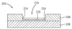
도 2a에 도시된 바와 같이, 유전체 층, 예컨대, 산화물 층(204)이 제1 Si 층(202) 위에 성장되거나, 형성되거나, 다른 방식으로 증착된다. 그 다음, 도 2b에 도시된 바와 같이, 절연체상 규소(SOI) 기판을 생성하기 위해 제2 Si 층(206)이 산화물 층(204) 위에 증착된다. 제2 Si 층(206)의 두께는 일반적으로, 임의의 적합한 두께, 예를 들어, 약 0.5 nm 내지 약 200 nm, 예컨대, 약 80 nm, 또는 약 1 미크론(㎛) 내지 약 10 ㎛, 예컨대, 약 5 ㎛이다.2A, a dielectric layer, such as an
그 다음, 도 2c에 도시된 바와 같이, 박막(208)이 제2 Si 층(206) 위에 증착된다. 박막(208)은 일반적으로, ALD를 포함하는(그러나 이에 제한되지 않음) 임의의 적합한 증착 프로세스에 의해 증착되고, 일반적으로, 약 60 나노미터 미만, 약 5 nm 미만, 약 2 nm 미만 또는 약 1 nm 미만의 두께를 갖는다. 도 2c의 예에서, 박막(208)은 산화규소(SiO) 막이다.Then, as shown in FIG. 2C, a
도 2d에 도시된 바와 같이, 박막(208)은 적어도 하나의 제1 피쳐(210)(하나가 도시됨) 및 하나 이상의 제2 피쳐(212)(2개가 도시됨)로 패터닝된다. 패터닝은 일반적으로, 표준 리소그래피로 달성된다. 도 2d의 예에서, 제1 피쳐(210)는 제1 폭 또는 직경을 갖고, 제2 피쳐들(212)은 제2 폭 또는 직경을 갖는다. 제1 피쳐(210)는, 도 2d의 확대된 부분인 도 2e에 도시된 바와 같이, 제2 Si 층(206)의 제1 표면에 대응하는 바닥(216) 및 하나 이상의 측벽(214)을 포함한다. 제1 폭 또는 직경은 일반적으로, 약 10 나노미터(nm) 내지 약 100 nm, 예를 들어, 약 20 nm 내지 약 60 nm, 예컨대, 약 35 nm 내지 약 50 nm, 예컨대, 약 50 nm이다. 제2 폭 또는 직경은 일반적으로, 약 0.5 ㎛ 내지 약 10 ㎛, 예컨대, 약 1 ㎛이다.As shown in FIG. 2D, the
블록 공중합체(218)는, 도 2f에 도시된 바와 같이, 제1 피쳐(210)에 증착된다. 블록 공중합체(218)는 일반적으로, 도메인들로 상 분리되는 공중합체들로 구성된다. 도 2f에 도시된 바와 같이, 블록 공중합체(218)는 A 도메인(220) 및 B 도메인(222)으로 상 분리된다. A 도메인(220)은 환형으로 B 도메인(222) 주위에 있다. B 도메인(222)은 일반적으로, 제1 피쳐(210)의 중심에 또는 중심 근처에 중앙에 위치된다. 그 다음, 도 2g에 도시된 바와 같이, B 도메인(222)은 선택적으로 식각된다. 제1 피쳐(210)는, 나머지 유전체 층이 제1 피쳐(210)의 바닥에 있도록 이전에 식각되었다. 나머지 블록 공중합체(218)는 유전체 층(224)의 식각에 대해 하드 마스크로서 작용한다. 따라서, 도 2h에 도시된 바와 같이, 나노포어(226)가 유전체 층(224)을 통해 형성된다.The
위에서 논의된 바와 같이, 도 2a-2h는 박막(208)을 통해 나노포어(226)를 형성하기 위한 예를 예시한다. 나노포어(226)를 형성하기 위한 임의의 적합한 방법들이 본원에서 또한 고려된다. 예를 들어, 나노포어는, 다른 포어 직경 감소 프로세스들, 예컨대, 주기적 원자 층 증착, 또는 화학 기상 증착, 및 유전체 물질의 식각, 또는 유전체 물질을 형성하기 위해 기판을 산화시키는 것 및 나노포어를 형성하기 위해 약한 지점 또는 이음부에서 유전체 물질을 분해하는 것에 의해 형성될 수 있다. 일부 양상들에서, 증착 및 식각의 하나의 완전한 주기가, 잘 제어된 나노포어를 형성하는 데에 적합할 것이지만; 다른 양상들에서는, 형성될 나노포어의 크기에 따라, 주기들의 다수의 반복들이, 잘 제어된 나노포어를 형성하는 데에 적합할 것이다.As discussed above, FIGS. 2A-2H illustrate an example for forming
나노포어(226)의 크기(즉, 직경)는 약 100 nm 이하이다. 일 양상에서, 나노포어(226)의 크기는 약 1 nm 내지 약 10 nm, 예를 들어, 약 2 nm 내지 약 3 nm, 예컨대, 약 2 nm이다. 다른 양상에서, 나노포어(226)의 크기는 약 0.5 nm 내지 약 5 nm, 예를 들어, 약 1 nm 내지 약 3 nm, 예컨대, 2 nm이다. 다른 양상에서, 나노포어(226)의 크기는 약 1.5 nm 내지 약 1.8 nm, 예컨대, 약 1.6 nm이고, 이는 대략, DNA의 단일 가닥의 크기이다. 다른 양상에서, 나노포어(226)의 크기는 약 2 nm 내지 약 3 nm, 예컨대, 약 2.8 nm이고, 이는 대략, 이중 가닥 DNA의 크기이다.The size (ie, diameter) of the
나노포어(226)가 형성된 후에, 도 2j에 도시된 바와 같이, 나노포어(226) 및 하나 이상의 제2 피쳐(212) 아래의 제2 Si 층(206)의 부분을 제거하기 위해 선택적 식각 프로세스가 사용된다. 제2 Si 층(206)의 부분을 선택적으로 식각하는 것은 일반적으로, 기판(200)을 식각 챔버에 위치시키는 것, 규소를 제거하기 위해 선택된 식각제를 도입하는 것, 및 제2 Si 층(206)의 부분을 제거하기 위해 기판(200)을 규소 식각제에 노출시키는 것을 포함한다. 예를 들어, 라디칼 기반 화학물질은 원자 수준 정밀도의, 제2 Si 층(206)의 제거를 위한 조정가능한 선택성을 제공하는 데에 사용된다. 선택된 식각제 및 라디칼들은 제2 Si 층을 박막(208)에 대해 선택적으로 식각한다. 예를 들어, SiO2:Si의 선택적 식각들의 비율은 약 1:2000이다. 선택적 식각을 수행하기 위한 챔버의 예는, 캘리포니아주 산타 클라라 소재의 어플라이드 머티어리얼스, 인코포레이티드로부터 입수가능한 프로듀서® 셀렉트라™(Producer® Selectra™) 식각 챔버이다.After the
전술한 예는 Si 층(206)을 선택적으로 식각하는 것을 고려하지만, 식각된 층은 일반적으로 임의의 적합한 고도로 식각가능한 층인 것이 고려된다.Although the above example considers selectively etching the
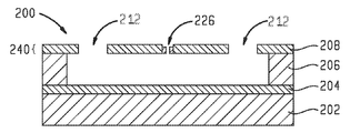
일단 제2 Si 층(206)의 부분이 선택적으로 식각되면, 도 2j에 도시된 바와 같이, 독립 멤브레인(240)이 박막(208)으로부터 형성된다. 독립 멤브레인(240)은 적어도 하나의 나노포어(226) 및 하나 이상의 개구부를 포함하며 여기서 하나 이상의 제2 피쳐(212)는 제2 Si 층(206) 위에 형성되었다. 독립 멤브레인(240)은 얇은데, 예를 들어, 약 50 나노미터 이하, 예컨대, 약 10 nm 미만, 약 5 nm 미만, 약 2 nm 미만, 또는 약 1 nm 미만이다. 독립 멤브레인(240)은 임의의 적합한 물질, 예컨대, 얇은 유전체 막이다.Once the portion of the
독립 멤브레인(240)을 형성하기 위한 개시된 방법들 동안 추가의 기판 처리가 선택적으로 수행된다. 예를 들어, 질화규소(SiN) 층과 같은 추가 층(228)이 독립 멤브레인(240)의 하나 이상의 부분 위에 형성된다. 추가적으로, 양의 전극(230) 및 음의 전극(232)이 독립 멤브레인(240)의 하나 이상의 부분 상에 증착되고, 따라서, 생물학적 응용들, 예컨대, DNA 서열분석에 적합한 반도체 기판을 형성한다. DNA 서열분석의 예에서, 제1 웰은 독립 멤브레인(240)의 일 측 상에 형성되고, 제2 웰은 독립 멤브레인(240)의 다른 측 상에 형성된다. 일 양상에서, DNA를 갖는 용액이 제1 웰에 배치되고 DNA가 없는 용액은 제2 웰에 배치된다. DNA가 음으로 대전되기 때문에, DNA는 전류를 따라 흘러, 나노포어(226)를 통해 제1 웰로부터 제2 웰로 이동할 것이다. DNA가 나노포어(226)를 통해 이동할 때, 나노포어( 226)를 통과하는 전류가 차단될 것이고, 예를 들어, 나노포어(226)를 통해 이동하는 염기를 식별함으로써 DNA가 서열분석될 수 있도록 전류의 변화가 측정된다. 다른 양상에서, DNA를 갖는 용액이 추가적으로 또는 대안적으로 제2 웰에 배치된다.Additional substrate processing is optionally performed during the disclosed methods for forming the independent membrane 240. For example, an
도 2a-2k는, 예로서, 작동들의 하나의 순서에 따른 프로세스 흐름의 다양한 스테이지들을 도시한다. 도 2a-2k에 도시되고 본원에 설명된 작동들은 임의의 적합한 순서로 수행될 수 있다는 것이 고려된다. 예를 들어, 추가의 실시예들에서, 제2 Si 층(206)의 부분은 나노포어(226)가 보호되는 동안 선택적으로 식각될 수 있고, 그 다음, 나노포어(226)는 선택적 식각이 완료되는 동안 보호되지 않을 수 있다.2A-2K show various stages of a process flow according to one order of operations, for example. It is contemplated that the operations shown in FIGS. 2A-2K and described herein can be performed in any suitable order. For example, in further embodiments, a portion of the
본 개시내용의 이점들은, 일반적으로 개별적으로 어드레싱가능한, 잘 제어된 나노포어들 및 나노포어 어레이들을 신속하게 형성하는 능력을 포함한다. 개시된 방법들은 일반적으로, 얇은 멤브레인을 통한, 크기 및 위치가 잘 제어된 나노포어들을 제공한다. 잘 제어된 크기의 나노포어들을 제조하는 방법들은 개선된 신호 대 잡음비들을 제공하는데, 이는 나노포어의 크기가, 나노포어를 통해 전달되고 있는 샘플, 예컨대, DNA의 단일 가닥의 크기와 유사하기 때문이며, 이는 나노포어를 통과하는 전류의 변화를 증가시킨다. 추가적으로, 잘 제어된 위치들을 갖는 나노포어들을 제조하는 방법들은 샘플, 예컨대, DNA가 나노포어를 자유롭게 통과하는 것을 가능하게 한다.Advantages of the present disclosure include the ability to rapidly form well-controlled nanopores and nanopore arrays, which are generally individually addressable. The disclosed methods generally provide well-controlled size and position of nanopores through a thin membrane. Methods of manufacturing well-controlled size nanopores provide improved signal-to-noise ratios because the size of the nanopore is similar to the size of a single strand of a sample, such as DNA, being transmitted through the nanopore, This increases the change in current through the nanopore. Additionally, methods of manufacturing nanopores with well-controlled positions allow samples, such as DNA, to freely pass through the nanopores.
본원에 설명된 방법들은 또한, 생물학적 응용들, 예컨대, DNA 서열분석을 위한 독립 멤브레인들을 제공하는데, 독립 멤브레인들은, 예를 들어, 1 nm 이하의 얇은 유전체이고, 염수 용액들(KCl)에 화학적으로 내성이고, 식각 프로세스들의 화학물질에 대한 높은 선택성을 갖고, 물리적으로 그리고 전기적으로 핀홀이 없고, 낮은 응력을 갖고, 습윤성이다. 독립 멤브레인이 얇을수록, 더 많은 전기장이 나노포어의 에지 주위에 집중될 것이고, 따라서, 본원에 설명된 방법들에 따라 제조된 독립 멤브레인들의 얇음은, 생물학적 응용들, 예컨대, DNA 염기 식별을 위한 사용 동안 높은 신호 대 잡음비를 허용한다.The methods described herein also provide independent membranes for biological applications, such as DNA sequencing, which are, for example, thin dielectrics of 1 nm or less, and chemically in saline solutions (KCl). It is resistant, has high selectivity for chemicals in etching processes, is physically and electrically free of pinholes, has low stress, and is wettable. The thinner the independent membrane, the more electric field will be concentrated around the edge of the nanopore, so the thinness of the independent membranes prepared according to the methods described herein can be used for biological applications such as DNA base identification. While allowing a high signal-to-noise ratio.
전술한 내용은 본 개시내용의 양상들에 관한 것이지만, 본 개시내용의 다른 및 추가적인 양상들은 그의 기본 범위로부터 벗어나지 않고 안출될 수 있으며, 그의 범위는 이하의 청구항들에 의해 결정된다.Although the foregoing is directed to aspects of the present disclosure, other and additional aspects of the present disclosure can be devised without departing from its basic scope, the scope of which is determined by the following claims.
Claims (15)
기판의 고도로 식각가능한 층 위에 박막을 갖는 기판을 제공하는 단계;
상기 고도로 식각가능한 층 위의 상기 박막을 통해 하나 이상의 나노포어를 형성하는 단계; 및
독립 멤브레인을 형성하기 위해, 상기 하나 이상의 나노포어 아래의 상기 고도로 식각가능한 층의 부분을 선택적으로 제거하는 단계를 포함하는, 기판을 형성하기 위한 방법.As a method for forming a substrate,
Providing a substrate having a thin film over a highly etchable layer of the substrate;
Forming one or more nanopores through the thin film on the highly etchable layer; And
A method for forming a substrate, comprising selectively removing a portion of the highly etchable layer below the one or more nanopores to form an independent membrane.
상기 고도로 식각가능한 층의 부분을 선택적으로 제거하는 단계는:
상기 기판을 식각 챔버에 위치시키는 것;
상기 고도로 식각가능한 층을 제거하기 위해 선택된 식각제를 상기 식각 챔버에 도입하는 것; 및
상기 고도로 식각가능한 층의 부분을 선택적으로 제거하기 위해 상기 기판을 상기 식각제에 노출시키는 것을 포함하는, 기판을 형성하기 위한 방법.According to claim 1,
The step of selectively removing portions of the highly etchable layer is:
Placing the substrate in an etch chamber;
Introducing a selected etchant into the etch chamber to remove the highly etchable layer; And
And exposing the substrate to the etchant to selectively remove portions of the highly etchable layer.
상기 독립 멤브레인은 유전체 막이고, 상기 고도로 식각가능한 층은 규소를 포함하는, 기판을 형성하기 위한 방법.According to claim 1,
The independent membrane is a dielectric film, and the highly etchable layer comprises silicon.
상기 독립 멤브레인의 적어도 일 측 상에 생물학적 샘플을 퇴적시키는 단계; 및
상기 생물학적 샘플을 상기 독립 멤브레인의 상기 하나 이상의 나노포어를 통해 지향시킴으로써 상기 생물학적 샘플을 분석하는 단계를 더 포함하는, 기판을 형성하기 위한 방법.According to claim 1,
Depositing a biological sample on at least one side of the independent membrane; And
And analyzing the biological sample by directing the biological sample through the one or more nanopores of the independent membrane.
상기 하나 이상의 나노포어의 각각의 직경은 약 100 나노미터 이하이고, 상기 독립 멤브레인의 두께는 약 50 나노미터 이하인, 기판을 형성하기 위한 방법.According to claim 1,
A method for forming a substrate, wherein each diameter of the one or more nanopores is about 100 nanometers or less, and the thickness of the independent membrane is about 50 nanometers or less.
기판의 고도로 식각가능한 층 위에 박막을 갖는 기판을 제공하는 단계;
포어 직경 감소 프로세스를 사용하여, 상기 고도로 식각가능한 층 위의 상기 박막을 통해 하나 이상의 나노포어를 형성하는 단계; 및
얇은 독립 멤브레인을 형성하기 위해, 상기 하나 이상의 나노포어 아래의 상기 고도로 식각가능한 층의 부분을 선택적으로 제거하는 단계를 포함하는, 기판을 형성하기 위한 방법.As a method for forming a substrate,
Providing a substrate having a thin film over a highly etchable layer of the substrate;
Forming one or more nanopores through the thin film over the highly etchable layer using a pore diameter reduction process; And
A method for forming a substrate, comprising selectively removing a portion of the highly etchable layer below the one or more nanopores to form a thin independent membrane.
상기 고도로 식각가능한 층의 부분을 선택적으로 제거하는 단계는:
상기 기판을 상기 고도로 식각가능한 층의 부분을 선택적으로 제거하도록 선택된 식각제에 노출시키는 것을 포함하는, 기판을 형성하기 위한 방법.The method of claim 6,
The step of selectively removing portions of the highly etchable layer is:
And exposing the substrate to an etchant selected to selectively remove portions of the highly etchable layer.
상기 독립 멤브레인의 적어도 일 측 상에 생물학적 샘플을 퇴적시키는 단계; 및
상기 생물학적 샘플을 상기 독립 멤브레인의 상기 하나 이상의 나노포어를 통해 지향시킴으로써 상기 생물학적 샘플을 분석하는 단계를 더 포함하는, 기판을 형성하기 위한 방법.The method of claim 6,
Depositing a biological sample on at least one side of the independent membrane; And
And analyzing the biological sample by directing the biological sample through the one or more nanopores of the independent membrane.
상기 포어 직경 감소 프로세스는:
상기 박막에 적어도 하나의 제1 피쳐를 형성하는 단계;
상기 제1 피쳐에 블록 공중합체를 증착시키는 단계 ― 상기 블록 공중합체는 적어도 제1 도메인 및 제2 도메인을 포함함 ―; 및
상기 제2 도메인을 식각하는 단계를 포함하는, 기판을 형성하기 위한 방법.The method of claim 6,
The pore diameter reduction process is:
Forming at least one first feature in the thin film;
Depositing a block copolymer on the first feature, the block copolymer comprising at least a first domain and a second domain; And
And etching the second domain.
상기 포어 직경 감소 프로세스는:
상기 박막에 적어도 하나의 제1 피쳐를 형성하는 단계;
상기 적어도 하나의 제1 피쳐 위에 유전체 물질을 증착시키는 단계; 및
상기 적어도 하나의 제1 피쳐 위의 상기 유전체 물질의 부분을 식각하는 단계를 포함하는, 기판을 형성하기 위한 방법.The method of claim 6,
The pore diameter reduction process is:
Forming at least one first feature in the thin film;
Depositing a dielectric material over the at least one first feature; And
And etching a portion of the dielectric material over the at least one first feature.
상기 방법은:
적어도 하나의 나노포어가 형성될 때까지, 상기 유전체 물질을 증착시키는 단계 및 상기 유전체 물질의 부분을 식각하는 단계를 반복하는 것을 더 포함하는, 기판을 형성하기 위한 방법.The method of claim 10,
The method is:
And repeating depositing the dielectric material and etching a portion of the dielectric material until at least one nanopore is formed.
상기 포어 직경 감소 프로세스는:
상기 박막에 적어도 하나의 제1 피쳐를 형성하는 단계;
적어도 하나의 개구부를 채우기 위해 상기 기판 위에 유전체 물질를 형성하기 위해서 상기 기판을 산화시키는 단계 ― 상기 유전체 물질은 상기 유전체 물질에 형성된 적어도 하나의 이음부를 가짐 ―; 및
적어도 하나의 나노포어를 형성하기 위해 상기 적어도 하나의 이음부를 활용하는 단계를 포함하는, 기판을 형성하기 위한 방법.The method of claim 6,
The pore diameter reduction process is:
Forming at least one first feature in the thin film;
Oxidizing the substrate to form a dielectric material over the substrate to fill at least one opening, the dielectric material having at least one seam formed in the dielectric material; And
And utilizing the at least one seam to form at least one nanopore.
상기 박막 위에 하나 이상의 추가적인 층을 증착시키는 단계; 및
상기 박막 위에 양의 전극 및 음의 전극을 증착시키는 단계를 더 포함하는, 기판을 형성하기 위한 방법.The method of claim 6,
Depositing one or more additional layers on the thin film; And
A method for forming a substrate, further comprising depositing a positive electrode and a negative electrode on the thin film.
제1 규소 층;
상기 제1 규소 층 위에 배치된 유전체 층;
상기 유전체 층의 부분 위에 배치된 제2 규소 층;
상기 제2 규소 층 위에 배치된 독립 멤브레인 ― 상기 독립 멤브레인은, 상기 독립 멤브레인을 통해 형성된, 적어도 하나의 나노포어 및 적어도 하나의 개구부를 가짐 ―;
상기 적어도 하나의 나노포어 아래에 배치된 제1 웰; 및
상기 적어도 하나의 나노포어 위에 배치된 제2 웰을 포함하는, 기판.As a substrate,
A first silicon layer;
A dielectric layer disposed over the first silicon layer;
A second silicon layer disposed over a portion of the dielectric layer;
An independent membrane disposed over the second silicon layer, the independent membrane having at least one nanopore and at least one opening formed through the independent membrane;
A first well disposed under the at least one nanopore; And
And a second well disposed over the at least one nanopore.
상기 제1 웰 및 상기 제2 웰 중 적어도 하나에 DNA 함유 유체를 포함하고, 상기 적어도 하나의 나노포어의 각각의 직경은 약 100 나노미터 이하이고, 상기 독립 멤브레인의 두께는 약 50 나노미터 이하인, 기판.
The method of claim 14,
A DNA-containing fluid in at least one of the first well and the second well, wherein each diameter of the at least one nanopore is about 100 nanometers or less, and the thickness of the independent membrane is about 50 nanometers or less, Board.
Priority Applications (1)
| Application Number | Priority Date | Filing Date | Title |
|---|---|---|---|
| KR1020227021066A KR102587775B1 (en) | 2017-09-22 | 2018-09-11 | Method to create a free-standing membrane for biological applications |
Applications Claiming Priority (5)
| Application Number | Priority Date | Filing Date | Title |
|---|---|---|---|
| US201762561976P | 2017-09-22 | 2017-09-22 | |
| US62/561,976 | 2017-09-22 | ||
| US16/122,171 US10830756B2 (en) | 2017-09-22 | 2018-09-05 | Method to create a free-standing membrane for biological applications |
| US16/122,171 | 2018-09-05 | ||
| PCT/US2018/050383 WO2019060168A1 (en) | 2017-09-22 | 2018-09-11 | Method to create a free-standing membrane for biological applications |
Related Child Applications (1)
| Application Number | Title | Priority Date | Filing Date |
|---|---|---|---|
| KR1020227021066A Division KR102587775B1 (en) | 2017-09-22 | 2018-09-11 | Method to create a free-standing membrane for biological applications |
Publications (2)
| Publication Number | Publication Date |
|---|---|
| KR20200044992A true KR20200044992A (en) | 2020-04-29 |
| KR102412947B1 KR102412947B1 (en) | 2022-06-24 |
Family
ID=65808006
Family Applications (2)
| Application Number | Title | Priority Date | Filing Date |
|---|---|---|---|
| KR1020207011448A KR102412947B1 (en) | 2017-09-22 | 2018-09-11 | How to Create a Freestanding Membrane for Biological Applications |
| KR1020227021066A KR102587775B1 (en) | 2017-09-22 | 2018-09-11 | Method to create a free-standing membrane for biological applications |
Family Applications After (1)
| Application Number | Title | Priority Date | Filing Date |
|---|---|---|---|
| KR1020227021066A KR102587775B1 (en) | 2017-09-22 | 2018-09-11 | Method to create a free-standing membrane for biological applications |
Country Status (6)
| Country | Link |
|---|---|
| US (1) | US10830756B2 (en) |
| EP (1) | EP3685434A4 (en) |
| JP (1) | JP7101765B2 (en) |
| KR (2) | KR102412947B1 (en) |
| CN (1) | CN111108591B (en) |
| WO (1) | WO2019060168A1 (en) |
Families Citing this family (2)
| Publication number | Priority date | Publication date | Assignee | Title |
|---|---|---|---|---|
| CA3018069C (en) | 2016-03-21 | 2019-09-03 | Two Pore Guys, Inc. | Wafer-scale assembly of insulator-membrane-insulator devices for nanopore sensing |
| US11486873B2 (en) | 2016-03-31 | 2022-11-01 | Ontera Inc. | Multipore determination of fractional abundance of polynucleotide sequences in a sample |
Citations (7)
| Publication number | Priority date | Publication date | Assignee | Title |
|---|---|---|---|---|
| WO2009045473A2 (en) * | 2007-10-02 | 2009-04-09 | President And Fellows Of Harvard College | Carbon nanotube synthesis for nanopore devices |
| KR20100126190A (en) * | 2009-05-22 | 2010-12-01 | 인터내셔널 비지네스 머신즈 코포레이션 | Method of forming sub-lithographic features using directed self-assembly of polymers |
| US20120021204A1 (en) * | 2010-07-26 | 2012-01-26 | International Business Machines Corporation | Structure and method to form nanopore |
| US20120108068A1 (en) * | 2010-11-03 | 2012-05-03 | Texas Instruments Incorporated | Method for Patterning Sublithographic Features |
| US20150284791A1 (en) * | 2014-04-08 | 2015-10-08 | International Business Machines Corporation | Reduction of entropic barrier of polyelectrolyte molecules in a nanopore device with agarose gel |
| US20160042971A1 (en) * | 2014-08-07 | 2016-02-11 | Tokyo Electron Limited | Method for Directed Self-Assembly and Pattern Curing |
| WO2016056887A1 (en) * | 2014-10-09 | 2016-04-14 | Mimos Berhad | Humidity sensor with nanoporous polyimide membranes and a method of fabrication thereof |
Family Cites Families (10)
| Publication number | Priority date | Publication date | Assignee | Title |
|---|---|---|---|---|
| US8512588B2 (en) | 2010-08-13 | 2013-08-20 | Lawrence Livermore National Security, Llc | Method of fabricating a scalable nanoporous membrane filter |
| EP2562135A1 (en) * | 2011-08-22 | 2013-02-27 | ETH Zurich | Method for producing and aligning nanowires and applications of such a method |
| BR112014027829B1 (en) | 2012-05-07 | 2021-03-23 | The University Of Ottawa | MANUFACTURE OF NANOPORES USING HIGH ELECTRIC FIELDS |
| JP2015525077A (en) * | 2012-06-15 | 2015-09-03 | ジェニア・テクノロジーズ・インコーポレイテッド | Chip configuration and highly accurate nucleic acid sequencing |
| EP3730205B1 (en) | 2013-03-15 | 2024-05-01 | President and Fellows of Harvard College | Method of surface wetting |
| US9046511B2 (en) * | 2013-04-18 | 2015-06-02 | International Business Machines Corporation | Fabrication of tunneling junction for nanopore DNA sequencing |
| US9230820B2 (en) | 2013-10-30 | 2016-01-05 | HGST Netherlands B.V. | Method for directed self-assembly (DSA) of a block copolymer (BCP) using a blend of a BCP with functional homopolymers |
| FR3023581B1 (en) | 2014-07-08 | 2016-07-15 | Snecma | MOUNTING AUBES IN PERIPHERY OF A TURBOMACHINE DISK |
| EP3234571B1 (en) * | 2014-12-19 | 2020-12-16 | The University of Ottawa | Integrating nanopore sensors within microfluidic channel arrays using controlled breakdown |
| US9945836B2 (en) * | 2015-04-23 | 2018-04-17 | International Business Machines Corporation | Field effect based nanopore device |
-
2018
- 2018-09-05 US US16/122,171 patent/US10830756B2/en active Active
- 2018-09-11 CN CN201880060589.0A patent/CN111108591B/en active Active
- 2018-09-11 JP JP2020516550A patent/JP7101765B2/en active Active
- 2018-09-11 KR KR1020207011448A patent/KR102412947B1/en active IP Right Grant
- 2018-09-11 KR KR1020227021066A patent/KR102587775B1/en active IP Right Grant
- 2018-09-11 EP EP18859772.8A patent/EP3685434A4/en not_active Withdrawn
- 2018-09-11 WO PCT/US2018/050383 patent/WO2019060168A1/en unknown
Patent Citations (7)
| Publication number | Priority date | Publication date | Assignee | Title |
|---|---|---|---|---|
| WO2009045473A2 (en) * | 2007-10-02 | 2009-04-09 | President And Fellows Of Harvard College | Carbon nanotube synthesis for nanopore devices |
| KR20100126190A (en) * | 2009-05-22 | 2010-12-01 | 인터내셔널 비지네스 머신즈 코포레이션 | Method of forming sub-lithographic features using directed self-assembly of polymers |
| US20120021204A1 (en) * | 2010-07-26 | 2012-01-26 | International Business Machines Corporation | Structure and method to form nanopore |
| US20120108068A1 (en) * | 2010-11-03 | 2012-05-03 | Texas Instruments Incorporated | Method for Patterning Sublithographic Features |
| US20150284791A1 (en) * | 2014-04-08 | 2015-10-08 | International Business Machines Corporation | Reduction of entropic barrier of polyelectrolyte molecules in a nanopore device with agarose gel |
| US20160042971A1 (en) * | 2014-08-07 | 2016-02-11 | Tokyo Electron Limited | Method for Directed Self-Assembly and Pattern Curing |
| WO2016056887A1 (en) * | 2014-10-09 | 2016-04-14 | Mimos Berhad | Humidity sensor with nanoporous polyimide membranes and a method of fabrication thereof |
Non-Patent Citations (2)
| Title |
|---|
| Axel Fanget 등, "Nanopore Integrated Nanogaps for DNA Detection", Nano Letters, 2013.12.06., Vol. 14, No. 1, 페이지 244-249* * |
| Miao Zhang 등, "Oxidation of nanopores in a silicon membrane: self-limiting formation of sub-10nm circular openings", Nanotechnology, 2014.08.12., Vol. 25, No. 35.* * |
Also Published As
| Publication number | Publication date |
|---|---|
| KR102587775B1 (en) | 2023-10-12 |
| US20190094203A1 (en) | 2019-03-28 |
| EP3685434A1 (en) | 2020-07-29 |
| WO2019060168A1 (en) | 2019-03-28 |
| KR20220095250A (en) | 2022-07-06 |
| KR102412947B1 (en) | 2022-06-24 |
| JP2020534009A (en) | 2020-11-26 |
| CN111108591B (en) | 2021-06-08 |
| EP3685434A4 (en) | 2021-06-16 |
| JP7101765B2 (en) | 2022-07-15 |
| US10830756B2 (en) | 2020-11-10 |
| CN111108591A (en) | 2020-05-05 |
Similar Documents
| Publication | Publication Date | Title |
|---|---|---|
| US10994991B2 (en) | Method to reduce pore diameter using atomic layer deposition and etching | |
| US8558326B2 (en) | Semiconductor devices having nanochannels confined by nanometer-spaced electrodes | |
| US20220227622A1 (en) | Pore formation in a substrate | |
| KR102587775B1 (en) | Method to create a free-standing membrane for biological applications | |
| US20190094179A1 (en) | Method for simple fluidic addressing of a nanopore | |
| KR102544057B1 (en) | Methods for forming nanopores and resulting structures | |
| KR20220004792A (en) | double pore sensors |
Legal Events
| Date | Code | Title | Description |
|---|---|---|---|
| E902 | Notification of reason for refusal | ||
| AMND | Amendment | ||
| E601 | Decision to refuse application | ||
| AMND | Amendment | ||
| X701 | Decision to grant (after re-examination) | ||
| GRNT | Written decision to grant |