KR20200022792A - Battery pack substrate and Battery pack substrate accessing system - Google Patents
Battery pack substrate and Battery pack substrate accessing system Download PDFInfo
- Publication number
- KR20200022792A KR20200022792A KR1020180098860A KR20180098860A KR20200022792A KR 20200022792 A KR20200022792 A KR 20200022792A KR 1020180098860 A KR1020180098860 A KR 1020180098860A KR 20180098860 A KR20180098860 A KR 20180098860A KR 20200022792 A KR20200022792 A KR 20200022792A
- Authority
- KR
- South Korea
- Prior art keywords
- grooves
- terminal
- battery pack
- microcontroller
- terminals
- Prior art date
Links
- 239000000758 substrate Substances 0.000 title claims abstract description 56
- 239000004020 conductor Substances 0.000 claims abstract description 10
- 238000000034 method Methods 0.000 claims description 15
- 230000000052 comparative effect Effects 0.000 description 4
- PXHVJJICTQNCMI-UHFFFAOYSA-N Nickel Chemical compound [Ni] PXHVJJICTQNCMI-UHFFFAOYSA-N 0.000 description 3
- WHXSMMKQMYFTQS-UHFFFAOYSA-N Lithium Chemical compound [Li] WHXSMMKQMYFTQS-UHFFFAOYSA-N 0.000 description 2
- 238000009529 body temperature measurement Methods 0.000 description 2
- 238000007599 discharging Methods 0.000 description 2
- 229910052744 lithium Inorganic materials 0.000 description 2
- 238000012986 modification Methods 0.000 description 2
- 230000004048 modification Effects 0.000 description 2
- 230000001151 other effect Effects 0.000 description 2
- OJIJEKBXJYRIBZ-UHFFFAOYSA-N cadmium nickel Chemical compound [Ni].[Cd] OJIJEKBXJYRIBZ-UHFFFAOYSA-N 0.000 description 1
- 238000004891 communication Methods 0.000 description 1
- 238000011161 development Methods 0.000 description 1
- 230000000694 effects Effects 0.000 description 1
- 238000004146 energy storage Methods 0.000 description 1
- 230000006870 function Effects 0.000 description 1
- 230000003446 memory effect Effects 0.000 description 1
- 239000007769 metal material Substances 0.000 description 1
- 229910052759 nickel Inorganic materials 0.000 description 1
- 229910000652 nickel hydride Inorganic materials 0.000 description 1
- QELJHCBNGDEXLD-UHFFFAOYSA-N nickel zinc Chemical compound [Ni].[Zn] QELJHCBNGDEXLD-UHFFFAOYSA-N 0.000 description 1
- 238000012545 processing Methods 0.000 description 1
- 238000011160 research Methods 0.000 description 1
- 238000000926 separation method Methods 0.000 description 1
- 238000012546 transfer Methods 0.000 description 1
Images


Classifications
-
- H—ELECTRICITY
- H01—ELECTRIC ELEMENTS
- H01R—ELECTRICALLY-CONDUCTIVE CONNECTIONS; STRUCTURAL ASSOCIATIONS OF A PLURALITY OF MUTUALLY-INSULATED ELECTRICAL CONNECTING ELEMENTS; COUPLING DEVICES; CURRENT COLLECTORS
- H01R12/00—Structural associations of a plurality of mutually-insulated electrical connecting elements, specially adapted for printed circuits, e.g. printed circuit boards [PCB], flat or ribbon cables, or like generally planar structures, e.g. terminal strips, terminal blocks; Coupling devices specially adapted for printed circuits, flat or ribbon cables, or like generally planar structures; Terminals specially adapted for contact with, or insertion into, printed circuits, flat or ribbon cables, or like generally planar structures
- H01R12/50—Fixed connections
- H01R12/51—Fixed connections for rigid printed circuits or like structures
- H01R12/55—Fixed connections for rigid printed circuits or like structures characterised by the terminals
-
- H—ELECTRICITY
- H01—ELECTRIC ELEMENTS
- H01M—PROCESSES OR MEANS, e.g. BATTERIES, FOR THE DIRECT CONVERSION OF CHEMICAL ENERGY INTO ELECTRICAL ENERGY
- H01M10/00—Secondary cells; Manufacture thereof
- H01M10/42—Methods or arrangements for servicing or maintenance of secondary cells or secondary half-cells
- H01M10/425—Structural combination with electronic components, e.g. electronic circuits integrated to the outside of the casing
-
- H—ELECTRICITY
- H05—ELECTRIC TECHNIQUES NOT OTHERWISE PROVIDED FOR
- H05K—PRINTED CIRCUITS; CASINGS OR CONSTRUCTIONAL DETAILS OF ELECTRIC APPARATUS; MANUFACTURE OF ASSEMBLAGES OF ELECTRICAL COMPONENTS
- H05K2201/00—Indexing scheme relating to printed circuits covered by H05K1/00
- H05K2201/10—Details of components or other objects attached to or integrated in a printed circuit board
- H05K2201/10007—Types of components
- H05K2201/10037—Printed or non-printed battery
-
- Y—GENERAL TAGGING OF NEW TECHNOLOGICAL DEVELOPMENTS; GENERAL TAGGING OF CROSS-SECTIONAL TECHNOLOGIES SPANNING OVER SEVERAL SECTIONS OF THE IPC; TECHNICAL SUBJECTS COVERED BY FORMER USPC CROSS-REFERENCE ART COLLECTIONS [XRACs] AND DIGESTS
- Y02—TECHNOLOGIES OR APPLICATIONS FOR MITIGATION OR ADAPTATION AGAINST CLIMATE CHANGE
- Y02E—REDUCTION OF GREENHOUSE GAS [GHG] EMISSIONS, RELATED TO ENERGY GENERATION, TRANSMISSION OR DISTRIBUTION
- Y02E60/00—Enabling technologies; Technologies with a potential or indirect contribution to GHG emissions mitigation
- Y02E60/10—Energy storage using batteries
Abstract
Description
본 발명은 배터리 팩 기판 및 배터리 팩 기판 접속 시스템에 관한 것으로서, 보다 상세하게는 배터리 팩 기판에 접속하는 과정에서 보안성이 강화된 배터리 팩 기판 및 효과적으로 배터리 팩 기판에 접속할 수 있는 배터리 팩 기판 접속 시스템에 관한 것이다.The present invention relates to a battery pack substrate and a battery pack substrate connection system, and more particularly, to a battery pack substrate with enhanced security and a battery pack substrate connection system capable of effectively connecting to a battery pack substrate in a process of connecting to a battery pack substrate. It is about.
근래에 들어서, 노트북, 비디오 카메라, 휴대용 전화기 등과 같은 휴대용 전자 제품의 수요가 급격하게 증대되고, 에너지 저장용 축전지, 로봇, 위성 등의 개발이 본격화됨에 따라, 반복적인 충방전이 가능한 고성능 이차 전지에 대한 연구가 활발히 진행되고 있다.In recent years, as the demand for portable electronic products such as laptops, video cameras, mobile phones, and the like is rapidly increasing, and development of energy storage batteries, robots, satellites, and the like is in earnest, high-performance secondary batteries capable of repeating charging and discharging are available. Research is actively being conducted.
현재 상용화된 이차 전지로는 니켈 카드뮴 전지, 니켈 수소 전지, 니켈 아연 전지 및 리튬 이차 전지 등이 있는데, 이 중에서 리튬 이차 전지는 니켈 계열의 이차 전지에 비해 메모리 효과가 거의 일어나지 않아 충방전이 자유롭고, 자가 방전율이 매우 낮으며 에너지 밀도가 높다는 등의 장점으로 인해 많은 각광을 받고 있다.Commercially available secondary batteries include nickel cadmium batteries, nickel hydride batteries, nickel zinc batteries, and lithium secondary batteries. Among them, lithium secondary batteries have almost no memory effect compared to nickel-based secondary batteries, and thus are free of charge and discharge. It is attracting much attention because of its low self discharge rate and high energy density.
배터리는 다양한 분야에서 이용되는데, 전기 구동 차량 또는 스마트 그리드 시스템과 같이 최근에 배터리가 많이 활용되는 분야는 큰 용량을 필요로 하는 경우가 많다. 배터리 팩의 용량을 증가하기 위해서는 이차 전지, 즉 배터리 셀 자체의 용량을 증가시키는 방법이 있을 수 있겠지만, 이 경우 용량 증대 효과가 크지 않고, 이차 전지의 크기 확장에 물리적 제한이 있으며 관리가 불편하다는 단점을 갖는다. 따라서, 통상적으로는 다수의 배터리 모듈이 직렬 및 병렬로 연결된 배터리 팩이 널리 이용된다.Batteries are used in various fields. In recent years, battery-intensive fields such as electric powered vehicles or smart grid systems often require large capacity. In order to increase the capacity of the battery pack, there may be a method of increasing the capacity of the secondary battery, that is, the battery cell itself. However, in this case, the capacity increase effect is not great, and there are physical limitations on the size expansion of the secondary battery and inconvenience of management. Has Thus, battery packs are typically widely used in which a plurality of battery modules are connected in series and in parallel.
이러한 배터리 팩에는, 배터리의 전압, 전류 및 온도 등을 측정하고 배터리의 충방전을 제어할 수 있도록 구성된 다수의 칩(chip)과 전기 회로가 구비된 배터리 팩 기판이 구비된다. 예를 들어, 배터리 팩 기판에는, 마이크로 컨트롤러와 메모리 디바이스와 같은 칩이 구비될 수 있다.The battery pack includes a battery pack substrate having a plurality of chips and electrical circuits configured to measure a voltage, a current, a temperature, and the like of the battery and to control charging and discharging of the battery. For example, the battery pack substrate may be equipped with chips such as microcontrollers and memory devices.
배터리 팩 기판에 구비된 마이크로 컨트롤러는, 마이크로 컨트롤러에 구비된 소프트웨어를 업로드 또는 다운로드 하거나, 마이크로 컨트롤러를 디버깅(debugging) 하기 위해 마이크로 컨트롤러에 접속할 필요성이 있다.The microcontroller included in the battery pack substrate needs to be connected to the microcontroller in order to upload or download the software included in the microcontroller or to debug the microcontroller.
하지만, 종래 배터리 팩 기판에 구비된 마이크로 컨트롤러 접속용 커넥터는, 마이크로 컨트롤러에 접근이 허락된 개발자 이외에 접근이 허락되지 않은 해커 등이 접근할 수 있어 보안성이 취약한 단점이 있다.However, the microcontroller connection connector provided in the conventional battery pack board has a disadvantage in that security is weak because a hacker or the like who is not allowed access to the microcontroller is accessible.
본 발명은 위와 같은 종래 기술의 배경하에 창안된 것으로서, 배터리 팩 기판에 접속하는 과정에서 보안성이 강화된 배터리 팩 기판 및 효과적으로 배터리 팩 기판에 접속할 수 있는 개선된 배터리 팩 기판 접속 시스템에 관한 것이다.The present invention has been made under the background of the prior art, and relates to a battery pack substrate with improved security in the process of connecting to a battery pack substrate and an improved battery pack substrate connection system capable of effectively connecting to a battery pack substrate.
본 발명의 다른 목적 및 장점들은 하기의 설명에 의해서 이해될 수 있으며, 본 발명의 실시예에 의해 보다 분명하게 알게 될 것이다. 또한, 본 발명의 목적 및 장점들은 특허청구범위에 나타난 수단 및 그 조합에 의해 실현될 수 있음을 쉽게 알 수 있을 것이다.Other objects and advantages of the present invention can be understood by the following description, and will be more clearly understood by the embodiments of the present invention. It will also be readily apparent that the objects and advantages of the present invention can be realized by the means and combinations thereof indicated in the claims.
상기와 같은 목적을 달성하기 위한 본 발명의 일 실시예에 따른 배터리 팩 기판은, 마이크로 컨트롤러; 판상으로 구성되며, 상기 마이크로 컨트롤러가 적어도 일면에 장착되고, 적어도 일면에 복수의 홈이 형성된 보드; 전도성 재질로 이루어지고, 상기 복수의 홈에 각각 필링 되도록 구성된 복수의 단자; 및 상기 보드에 실장되고, 상기 복수의 단자와 상기 마이크로 컨트롤러 사이를 전기적으로 연결하도록 구성된 신호 경로를 포함한다.Battery pack substrate according to an embodiment of the present invention for achieving the above object, a microcontroller; A board having a plate shape, the microcontroller mounted on at least one surface, and having a plurality of grooves formed on at least one surface thereof; A plurality of terminals made of a conductive material and configured to be respectively filled in the plurality of grooves; And a signal path mounted on the board and configured to electrically connect between the plurality of terminals and the microcontroller.
또한, 상기 복수의 단자는, 제1 단자 및 제2 단자를 포함하며, 상기 제1 단자는, 상기 마이크로 컨트롤러의 접속핀과 전기적으로 연결되도록 구성되고, 상기 제2 단자는, 상기 마이크로 컨트롤러와 전기적으로 연결되지 않도록 구성될 수 있다.The plurality of terminals may include a first terminal and a second terminal, wherein the first terminal is configured to be electrically connected to a connection pin of the microcontroller, and the second terminal is electrically connected to the microcontroller. It may be configured not to be connected to.
또한, 상기 복수의 홈은, 상기 제1 단자가 필링된 제1 홈 및 상기 제2 단자가 필링된 제2 홈을 포함하며, 상기 제1 홈 및 상기 제2 홈은, 각각 복수개 구비되고, 상기 복수의 홈은, 적어도 하나의 상기 제2 홈이 적어도 2개의 상기 제1 홈 사이에 배치될 수 있다.The plurality of grooves may include a first groove filled with the first terminal and a second groove filled with the second terminal, and each of the first groove and the second groove may be provided in plural. In the plurality of grooves, at least one second groove may be disposed between at least two first grooves.
또한, 상기 복수의 홈은, 3개 이상의 상기 제1 홈이 서로 연결되어 이루는 다각형 내부에 적어도 하나의 상기 제2 홈이 포함되도록 배치될 수 있다.In addition, the plurality of grooves may be arranged such that at least one of the second grooves is included in a polygonal structure in which three or more first grooves are connected to each other.
또한, 상기 복수의 홈은, 상기 보드의 양면에 각각 형성될 수 있다.In addition, the plurality of grooves may be formed on both surfaces of the board, respectively.
또한, 상기 복수의 단자는, 상기 복수의 홈의 깊이 방향으로 상기 복수의 홈의 깊이 보다 낮은 높이로 각각 충진 될 수 있다.In addition, the plurality of terminals may be respectively filled to a height lower than the depth of the plurality of grooves in the depth direction of the plurality of grooves.
또한, 상기와 같은 목적을 달성하기 위한 본 발명의 일 실시예에 따른 배터리 팩 기판 접속 시스템은, 마이크로 컨트롤러와, 판상으로 구성되며, 상기 마이크로 컨트롤러가 적어도 일면에 장착되고, 적어도 일면에 복수의 홈이 형성된 보드와, 전도성 재질로 이루어지고, 상기 복수의 홈에 각각 필링 되도록 구성된 복수의 단자와, 상기 보드에 실장되고, 상기 복수의 단자와 상기 마이크로 컨트롤러 사이를 전기적으로 연결하도록 구성된 신호 경로를 포함하는 배터리 팩 기판; 상부에 상기 보드가 장착될 수 있도록 구성된 장착 유닛; 상하 방향으로 길게 연장된 부분이 형성된 복수의 핀을 구비하여 상기 복수의 단자에 전기적으로 접촉할 수 있도록 구성된 단자 접촉 유닛; 및 상기 단자 접촉 유닛과 전기적으로 연결되며, 외부 장치와 연결 가능하도록 구성된 연결 유닛을 포함한다.In addition, the battery pack board connection system according to an embodiment of the present invention for achieving the above object is composed of a microcontroller and a plate, the microcontroller is mounted on at least one surface, a plurality of grooves on at least one surface And a plurality of terminals formed of a conductive material and configured to be respectively filled in the plurality of grooves, and a signal path mounted on the board and configured to electrically connect the plurality of terminals to the microcontroller. A battery pack substrate; A mounting unit configured to mount the board thereon; A terminal contact unit having a plurality of pins extending in a vertical direction, the terminal contact unit being configured to electrically contact the plurality of terminals; And a connection unit electrically connected to the terminal contact unit and configured to be connectable with an external device.
또한, 본 발명의 일 실시예에 따른 배터리 팩 기판 접속 시스템은, 상기 장착 유닛과 소정 거리 이격되어 이격 공간에 상기 보드가 개재될 수 있도록 구성되고, 상기 장착 유닛 방향 및 반대 방향으로 양방향 이동 가능하도록 구성된 고정 유닛을 더 포함할 수 있다.In addition, the battery pack board connection system according to an embodiment of the present invention, the board is spaced apart from the mounting unit by a predetermined distance so as to be interposed in the space, so as to be able to move in both directions in the mounting unit and the opposite direction It may further comprise a fixed unit configured.
또한, 상기 단자 접촉 유닛은, 상기 고정 유닛과 상기 장착 유닛에 각각 구비되어 서로를 향하는 방향으로 돌출 연장된 형태로 구성되며, 상기 복수의 단자에 대응하는 위치에 장착되어 상기 복수의 단자에 전기적으로 접촉할 수 있도록 구성된 복수의 핀을 포함할 수 있다.In addition, the terminal contact unit is provided in each of the fixed unit and the mounting unit is configured to protrude in a direction toward each other, and is mounted at a position corresponding to the plurality of terminals to be electrically connected to the plurality of terminals It may include a plurality of pins configured to be in contact.
또한, 상기 복수의 단자는, 제1 단자 및 제2 단자를 포함하며, 상기 제1 단자는, 상기 마이크로 컨트롤러의 접속핀과 전기적으로 연결되도록 구성되고, 상기 제2 단자는, 상기 마이크로 컨트롤러와 전기적으로 연결되지 않도록 구성될 수 있다.The plurality of terminals may include a first terminal and a second terminal, wherein the first terminal is configured to be electrically connected to a connection pin of the microcontroller, and the second terminal is electrically connected to the microcontroller. It may be configured not to be connected to.
또한, 상기 복수의 홈은, 상기 제1 단자가 필링된 제1 홈 및 상기 제2 단자가 필링된 제2 홈을 포함하며, 상기 제1 홈 및 상기 제2 홈은, 각각 복수개 구비되고, 상기 복수의 홈은, 적어도 하나의 상기 제2 홈이 적어도 2개의 상기 제1 홈 사이에 배치될 수 있다.The plurality of grooves may include a first groove filled with the first terminal and a second groove filled with the second terminal, and each of the first groove and the second groove may be provided in plural. In the plurality of grooves, at least one second groove may be disposed between at least two first grooves.
또한, 상기 복수의 홈은, 3개 이상의 상기 제1 홈이 서로 연결되어 이루는 다각형 내부에 적어도 하나의 상기 제2 홈이 포함되도록 배치될 수 있다.In addition, the plurality of grooves may be arranged such that at least one of the second grooves is included in a polygonal structure in which three or more first grooves are connected to each other.
본 발명의 일 측면에 의하면, 복수의 단자 중 허수인 단자를 통해 마이크로 컨트롤러에 접근이 허락된 개발자 이외에 해커 등의 접근이 어렵도록 하여 보안성을 강화할 수 있는 장점이 있다.According to an aspect of the present invention, there is an advantage that it is possible to enhance the security by making it difficult for hackers and others to access the microcontroller through the imaginary terminal among the plurality of terminals.
이외에도 본 발명은 다른 다양한 효과를 가질 수 있으며, 이러한 본 발명의 다른 효과들은 하기의 설명에 의해서 이해될 수 있고, 본 발명의 실시예에 의해 보다 분명하게 알 수 있다.In addition to the present invention may have a variety of other effects, such other effects of the present invention can be understood by the following description, it will be more clearly understood by the embodiments of the present invention.
본 명세서에 첨부되는 다음의 도면들은 본 발명의 바람직한 실시예를 예시하는 것이며, 후술하는 발명의 상세한 설명과 함께 본 발명의 기술사상을 더욱 이해시키는 역할을 하는 것이므로, 본 발명은 그러한 도면에 기재된 사항에만 한정되어 해석되어서는 아니 된다.
도 1은, 본 발명의 일 실시예에 따른 배터리 팩 기판 접속 시스템의 일부 구성을 개략적으로 나타내는 사시도이다.
도 2는, 본 발명의 비교예에 따른 배터리 팩 기판 접속 방법을 나타내는 사시도이다.
도 3은, 본 발명의 일 실시예에 따른 배터리 팩 기판의 일부 구성을 개략적으로 나타내는 사시도이다.
도 4는, 본 발명의 일 실시예에 따른 복수의 홈이 배터리 팩 기판에 형성된 구성을 개략적으로 나타내는 평면도이다.
도 5는, 본 발명의 일 실시예에 따른 배터리 팩 기판의 일부 구성을 개략적으로 나타내는 단면도이다.
도 6은, 본 발명의 다른 실시예에 따른 배터리 팩 기판의 일부 구성을 개략적으로 나타내는 단면도이다.
도 7은, 본 발명의 일 실시예에 따른 배터리 팩 기판 접속 시스템의 일부 구성을 개략적으로 나타내는 정면도이다.
도 8은, 본 발명의 일 실시예에 따른 고정 유닛의 일부 구성을 개략적으로 나타내는 평면도이다.
도 9는, 본 발명의 일 실시예에 따른 장착 유닛과 고정 유닛 사이에 배터리팩 기판이 장착된 구성을 개략적으로 나타내는 정면도이다.The following drawings attached to this specification are illustrative of preferred embodiments of the present invention, and together with the detailed description of the invention to serve to further understand the technical spirit of the present invention, the present invention is a matter described in such drawings It should not be construed as limited to.
1 is a perspective view schematically showing some components of a battery pack board connection system according to an embodiment of the present invention.
2 is a perspective view showing a battery pack substrate connecting method according to a comparative example of the present invention.
3 is a perspective view schematically illustrating some components of a battery pack substrate according to an exemplary embodiment of the present invention.
4 is a plan view schematically illustrating a configuration in which a plurality of grooves are formed in a battery pack substrate according to an embodiment of the present invention.
5 is a cross-sectional view schematically illustrating some components of a battery pack substrate according to an exemplary embodiment of the present invention.
6 is a cross-sectional view schematically showing some components of a battery pack substrate according to another embodiment of the present invention.
7 is a front view schematically showing a part of a configuration of a battery pack board connection system according to an embodiment of the present invention.
8 is a plan view schematically showing a part of a configuration of a fixing unit according to an embodiment of the present invention.
9 is a front view schematically illustrating a configuration in which a battery pack substrate is mounted between a mounting unit and a fixing unit according to an embodiment of the present invention.
이하, 첨부된 도면을 참조하여 본 발명의 바람직한 실시예를 상세히 설명하기로 한다. 이에 앞서, 본 명세서 및 청구범위에 사용된 용어나 단어는 통상적이거나 사전적인 의미로 한정해서 해석되어서는 안 되며, 발명자는 그 자신의 발명을 가장 최선의 방법으로 설명하기 위해 용어의 개념을 적절하게 정의할 수 있다는 원칙에 입각하여 본 발명의 기술적 사상에 부합하는 의미와 개념으로 해석되어야만 한다.Hereinafter, exemplary embodiments of the present invention will be described in detail with reference to the accompanying drawings. Prior to this, terms or words used in the present specification and claims should not be construed as being limited to the common or dictionary meanings, and the inventors should properly explain the concept of terms in order to best explain their own inventions. It should be interpreted as meaning and concept corresponding to the technical idea of the present invention based on the principle that it can be defined.
따라서, 본 명세서에 기재된 실시예와 도면에 도시된 구성은 본 발명의 가장 바람직한 일 실시예에 불과할 뿐이고 본 발명의 기술적 사상에 모두 대변하는 것은 아니므로, 본 출원시점에 있어서 이들을 대체할 수 있는 다양한 균등물과 변형예들이 있을 수 있음을 이해하여야 한다.Therefore, the embodiments described in the specification and the drawings shown in the drawings are only the most preferred embodiment of the present invention and do not represent all of the technical spirit of the present invention, various modifications that can be replaced at the time of the present application It should be understood that there may be equivalents and variations.
또한, 본 발명을 설명함에 있어 관련된 공지 구성 또는 기능에 대한 구체적인 설명이 본 발명의 요지를 흐릴 수 있다고 판정되는 경우에는 그 상세한 설명은 생략한다.In addition, in describing the present invention, when it is determined that the detailed description of the related well-known configuration or function may obscure the gist of the present invention, the detailed description thereof will be omitted.
명세서 전체에서, 어떤 부분이 어떤 구성요소를 "포함"한다고 할 때, 이는 특별히 반대되는 기재가 없는 한 다른 구성요소를 제외하는 것이 아니라, 다른 구성요소를 더 포함할 수 있다는 것을 의미한다. Throughout the specification, when a part is said to "include" a certain component, it means that it may further include other components, without excluding the other components unless otherwise stated.
덧붙여, 명세서 전체에서, 어떤 부분이 다른 부분과 "연결"되어 있다고 할 때, 이는 "직접적으로 연결"되어 있는 경우뿐만 아니라, 그 중간에 다른 소자를 사이에 두고 "간접적으로 연결"되어 있는 경우도 포함한다.In addition, throughout the specification, when a part is "connected" to another part, it is not only "directly connected" but also "indirectly connected" with another element in between. Include.
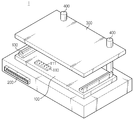
도 1은, 본 발명의 일 실시예에 따른 배터리 팩 기판 접속 시스템의 일부 구성을 개략적으로 나타내는 사시도이고, 도 3은, 본 발명의 일 실시예에 따른 배터리 팩 기판의 일부 구성을 개략적으로 나타내는 사시도이다.1 is a perspective view schematically showing a part of a battery pack board connection system according to an embodiment of the present invention, Figure 3 is a perspective view schematically showing a part of a battery pack board according to an embodiment of the present invention to be.
도 1 및 도 3을 참조하면, 본 발명의 일 실시예에 따른 배터리 팩 기판 접속 시스템(1)은, 배터리 팩 기판, 장착 유닛(100), 단자 접촉 유닛(110) 및 연결 유닛(200)을 포함한다.1 and 3, a battery pack
본 발명의 일 실시예에 따른 상기 배터리 팩 기판은, 마이크로 컨트롤러(10), 보드(20), 복수의 단자(23) 및 신호 경로(25)를 포함할 수 있다.The battery pack substrate according to an embodiment of the present invention may include a
상기 마이크로 컨트롤러(10)는, 배터리 팩 기판에 구비되어 배터리 관리 시스템(BMS)을 제어하도록 구성된 칩(Chip)일 수 있다. 예를 들어, 마이크로 컨트롤러(10)는, 배터리의 전압, 전류 및 온도 측정값을 수신하고, 상기 전압, 상기 전류 및 상기 온도 측정값을 기초로 배터리의 전하를 균등하게 할 수 있도록 배터리 밸런싱 동작을 수행할 수 있다. 이를 테면, 마이크로 컨트롤러(10)는, 상술한 바와 같은 동작을 수행하기 위해, 당업계에 알려진 프로세서, ASIC(Application-Specific Integrated Circuit), MCU(Micro Controller Unit), 다른 칩셋, 논리 회로, 레지스터, 통신 모뎀 및/또는 데이터 처리 장치 등을 선택적으로 포함하는 형태로 구현될 수 있다.The
또한, 도 3의 구성에 도시된 바와 같이, 마이크로 컨트롤러(10)는, 배터리 팩 기판에 장착될 수 있다. 예를 들어, 마이크로 컨트롤러(10)는, 배터리 팩 기판 상에 부착될 수 있다. 이를 테면, 마이크로 컨트롤러(10)는 배터리 팩 기판 상에 숄더링된 형태로 장착될 수 있다.In addition, as shown in the configuration of FIG. 3, the
상기 보드(20)는, 판상으로 구성될 수 있다. 또한, 보드(20)는, 마이크로 컨트롤러(10)가 적어도 일면에 장착될 수 있다. 예를 들어, 도 3의 구성에 도시된 바와 같이, 보드(20)는 판상으로 형성되어 일면에 마이크로 컨트롤러(10)가 장착될 수 있다.The
또한, 보드(20)는, 적어도 일면에 복수의 홈(21)이 형성될 수 있다. 예를 들어, 도 3의 구성에 도시된 바와 같이, 보드(20)는, 일면에 보드(20)의 내측 방향으로 오목하게 형성된 복수의 홈(21)이 배치될 수 있다.In addition, the
또한, 보드(20)는, 배터리 팩에 구비된 적어도 하나의 이차 전지와 연결되어, 이차 전지와 BMS 사이에서 정보를 전달하는 적어도 하나의 소자가 구비되어 있는 기판을 말한다. 예를 들어, 배터리 팩 기판은, 배터리 팩에 구비된 ICB(Integrated Circuit Board) 또는 PCB(Printed Circuit Board) 일 수 있다. 여기서, ICB 또는 PCB는 배터리 팩에 구비된 센싱 어셈블리에 장착되어, 이차 전지의 전극 리드로부터 센싱 된 정보를 BMS로 전달하는 집적 회로 기판을 의미할 수 있다.In addition, the
상기 복수의 단자(23)는, 전도성 재질로 이루어질 수 있다. 예를 들어, 복수의 단자(23)는, 전기 전도성 금속 재질로 이루어질 수 있다. 또한, 복수의 단자(23)는, 복수의 홈(21)에 각각 필링 되도록 구성될 수 있다. 예를 들어, 도 3의 구성에 도시된 바와 같이, 복수의 단자(23)는, 복수의 홈(21) 내부에 각각 필링 되도록 구성될 수 있다.The plurality of
상기 신호 경로(25)는, 보드(20)에 실장 될 수 있다. 예를 들어, 도 3의 구성에 도시된 바와 같이, 신호 경로(25)는, 보드(20)에 구비될 수 있다. 예를 들어, 신호 경로(25)는, 보드(20)의 표면에 인쇄될 수 있다. 또한, 신호 경로(25)는, 보드(20)의 내부에 매립되도록 구성될 수 있다. 다만, 도 3에 도시된 신호 경로(25)의 회로 인쇄 형태는 예시적인 것이며, 다른 형태로도 신호 경로(25)의 회로가 인쇄될 수 있다.The
또한, 신호 경로(25)는, 복수의 단자(23)와 마이크로 컨트롤러(10) 사이를 전기적으로 연결하도록 구성될 수 있다. 예를 들어, 도 3의 구성에 도시된 바와 같이, 신호 경로(25)는, 전기적 신호를 주고 받을 수 있도록 복수의 단자(23)와 마이크로 컨트롤러(10)의 접속핀(11) 사이를 각각 전기적으로 직접 연결할 수 있다. In addition, the
상기 장착 유닛(100)은, 상부에 보드(20)가 장착될 수 있도록 구성될 수 있다. 예를 들어, 도 1의 구성에 도시된 바와 같이, 장착 유닛(100)은, 판상으로 구성되어 일면에 보드(20)가 장착될 수 있다.The mounting
바람직하게는, 본 발명의 일 실시예에 따른 장착 유닛(100)은, 도 1의 구성에 도시된 바와 같이, 체결부(130)를 더 포함할 수 있다.Preferably, the mounting
상기 체결부(130)는, 도 1의 구성에 도시된 바와 같이, 장착 유닛(100)의 길이 방향으로 양측에 구비될 수 있다. 또한, 체결부(130)는, 2개의 체결부(130) 사이에 보드(20)가 체결될 수 있도록 2개의 체결부(130) 사이의 이격 거리가 보드(20)의 길이와 동일 또는 유사하도록 배치될 수 있다.As shown in the configuration of FIG. 1, the
상기 단자 접촉 유닛(110)은, 상하 방향으로 길게 연장된 부분이 형성된 복수의 핀(111)을 구비할 수 있다. 예를 들어, 도 1의 구성에 도시된 바와 같이, 단자 접촉 유닛(110)은, 일면에 상하 방향으로 길게 연장된 복수의 핀(111)을 구비할 수 있다.The
또한, 단자 접촉 유닛(110)은, 복수의 단자(23)에 전기적으로 접촉할 수 있도록 구성될 수 있다. 예를 들어, 도 1 및 도 3의 구성에 도시된 바와 같이, 단자 접촉 유닛(110)은, 배터리 팩 기판에 형성된 홈(21)의 위치에 대응하는 위치에 복수의 핀(111)이 구비될 수 있다. 또한, 단자 접촉 유닛(110)은, 복수의 핀(111)이 복수의 단자(23)에 각각 전기적으로 접촉할 수 있다. In addition, the
바람직하게는, 본 발명의 일 실시예에 따른 배터리 팩 기판 접속 시스템(1)은, 도 1의 구성에 도시된 바와 같이, 지지대(400)를 더 포함할 수 있다. 예를 들어, 상기 지지대(400)는, 장착 유닛(100)과 고정 유닛(300) 사이에 구비될 수 있다. 또한, 지지대(400)는, 고정 유닛(300)을 장착 유닛(100)의 방향과 장착 유닛(100)의 반대 방향으로 이동시킬 수 있다. 예를 들어, 지지대(400)는, 고정 유닛(300)을 이동시킬 수 있도록 모터를 구비할 수 있다.Preferably, the battery pack
상기 연결 유닛(200)은, 단자 접촉 유닛(110)과 전기적으로 연결될 수 있다. 예를 들어, 도 1의 구성에 도시된 바와 같이, 연결 유닛(200)은, 단자 접촉 유닛(110)에 구비된 복수의 핀(111)과 전기적으로 연결될 수 있다. The
또한, 연결 유닛(200)은, 외부 장치와 연결 가능하도록 구성될 수 있다. 예를 들어, 도 1의 구성에 도시된 바와 같이, 연결 유닛(200)은, 외부 장치의 커넥터가 결합될 수 있는 형태로 구성될 수 있다. 또한, 연결 유닛(200)은, 외부 장치의 커넥터가 연결 유닛(200)에 결합되는 경우, 복수의 핀(111)과 외부 장치 사이에서 전기적 신호를 주고 받을 수 있다.In addition, the
도 2는, 본 발명의 비교예에 따른 배터리 팩 기판 접속 방법을 나타내는 사시도이다.2 is a perspective view showing a battery pack substrate connecting method according to a comparative example of the present invention.
도 2를 참조하면, 본 발명의 비교예에 따른 배터리 팩 기판은, 커넥터(24)를 구비할 수 있다.Referring to FIG. 2, the battery pack board according to the comparative example of the present invention may include a
상기 커넥터(24)는, 배터리 팩 기판에 장착될 수 있다. 또한, 커넥터(24)는, 신호 경로(25)를 통해 마이크로 컨트롤러(10)의 접속핀(11)과 전기적으로 직접 연결될 수 있다.The
또한, 커넥터(24)는, 도 2의 구성에 도시된 바와 같이, 외부 장치의 커넥터(31)가 결합 가능하도록 구성될 수 있다. 여기서, 외부 장치의 커넥터(31)는 연결 선로(30)를 통해 외부 장치와 연결되어 전기적 신호를 주고 받을 수 있다.In addition, the
이와 같은 본 발명의 비교예에 따른 배터리 팩 기판은, 배터리 팩 기판에 구비된 커넥터(24)에 외부 장치의 커넥터(31)를 연결함으로써, 마이크로 컨트롤러(10)에 접속하여 마이크로 컨트롤러(10)의 소프트웨어를 업그레이드하거나, 프로그래밍 또는 디버깅할 수 있다. 그러나, 이 경우, 마이크로 컨트롤러(10)의 개발자 이외의 접속이 허가되지 않은 외부인(예를 들어, 해커)이 상기 커넥터(24)를 통해 마이크로 컨트롤러(10)를 해킹할 수 있어 보안에 취약하다는 단점이 있다.The battery pack substrate according to the comparative example of the present invention is connected to the
도 4는, 본 발명의 일 실시예에 따른 복수의 홈이 배터리 팩 기판에 형성된 구성을 개략적으로 나타내는 평면도이다. 또한, 도 5는, 본 발명의 일 실시예에 따른 배터리 팩 기판의 일부 구성을 개략적으로 나타내는 단면도이고, 도 6은, 본 발명의 다른 실시예에 따른 배터리 팩 기판의 일부 구성을 개략적으로 나타내는 단면도이다. 4 is a plan view schematically illustrating a configuration in which a plurality of grooves are formed in a battery pack substrate according to an embodiment of the present invention. 5 is a cross-sectional view schematically showing some components of a battery pack substrate according to an embodiment of the present invention, and FIG. 6 is a cross-sectional view schematically showing some components of a battery pack substrate according to another embodiment of the present invention. to be.
먼저, 도 3 및 도 5를 참조하면, 본 발명의 일 실시예에 따른 배터리 팩 기판은, 복수의 단자를 구비할 수 있다.First, referring to FIGS. 3 and 5, a battery pack substrate according to an exemplary embodiment of the present invention may include a plurality of terminals.
바람직하게는, 상기 복수의 단자(23)는, 제1 단자(23_a) 및 제2 단자(23_b)를 포함할 수 있다.Preferably, the plurality of
상기 제1 단자(23_a)는, 마이크로 컨트롤러(10)의 접속핀(11)과 전기적으로 연결되도록 구성될 수 있다. 예를 들어, 도 5의 구성에 도시된 바와 같이, 제1 단자(23_a)는, 전기 전도성 재질로 이루어질 수 있다. 또한, 제1 단자(23_a)는, 신호 경로(25)와 전기적으로 연결될 수 있다. 또한, 제1 단자(23_a)는, 신호 경로(25)를 통해 마이크로 컨트롤러(10)의 접속핀(11)과 전기적으로 연결될 수 있다. 예를 들어, 도 5의 구성에 도시된 바와 같이, 신호 경로(25)는, 보드(20) 내부에 매립되는 형태로 구성될 수 있다. The first terminal 23_a may be configured to be electrically connected to the
상기 제2 단자(23_b)는, 마이크로 컨트롤러(10)와 전기적으로 연결되지 않도록 구성될 수 있다. 예를 들어, 도 5의 구성에 도시된 바와 같이, 제2 단자(23_b)는, 전기 전도성 재질로 이루어질 수 있다. 또한, 제2 단자(23_b)는, 신호 경로(25)와 전기적으로 연결되지 않도록 구성될 수 있다. 이 경우, 제2 단자(23_b)는, 마이크로 컨트롤러(10)와 전기적으로 연결되지 않도록 구성될 수 있다.The second terminal 23_b may be configured not to be electrically connected to the
이와 같은 구성을 통해 본 발명의 일 실시예에 따른 배터리 팩 기판은, 배터리 팩 기판의 외부에서 육안상으로 확인하는 경우, 실제 마이크로 컨트롤러(10)의 접속핀(11)과 전기적으로 연결되는 단자를 쉽게 구별할 수 없도록 구성되어 보안성이 향상되는 효과가 있다.Through such a configuration, the battery pack substrate according to the exemplary embodiment of the present invention, when visually confirmed from the outside of the battery pack substrate, the terminal electrically connected to the
도 3 및 도 4를 참조하면, 본 발명의 일 실시예에 따른 복수의 홈(21)은, 제1 홈(21_a) 및 제2 홈(21_b)을 포함할 수 있다.3 and 4, the plurality of
상기 제1 홈(21_a)은, 상기 제1 단자(23_a)가 필링 될 수 있다. 또한, 상기 제2 홈(21_b)은, 상기 제2 단자(23_b)가 필링 될 수 있다. 예를 들어, 도 3 및 도 4의 구성에 도시된 바와 같이, 복수의 홈(21)은, 배터리 팩 기판의 A영역 내에 형성될 수 있다. 또한, 제1 홈(21_a) 내부에는 전기 전도성 재질로 이루어진 제1 단자(23_a)가 필링 될 수 있다. 또한, 제2 홈(21_b) 내부에는 전기 전도성 재질로 이루어진 제2 단자(23_b)가 필링 될 수 있다.The first terminal 23_a may be filled in the first groove 21_a. In addition, the second terminal 21_b may be filled with the second terminal 23_b. For example, as shown in the configuration of FIGS. 3 and 4, the plurality of
또한, 상기 제1 홈(21_a) 및 상기 제2 홈(21_b)은, 각각 복수개 구비될 수 있다. 예를 들어, 도 4의 구성에 도시된 바와 같이, 제1 홈(21_a) 및 제2 홈(21_b)은, 각각 복수개가 배치될 수 있다. In addition, each of the first grooves 21_a and the second grooves 21_b may be provided in plurality. For example, as illustrated in the configuration of FIG. 4, a plurality of first grooves 21_a and second grooves 21_b may be disposed, respectively.
또한, 복수의 홈(21)은, 적어도 하나의 제2 홈(21_b)이 적어도 2개의 제1 홈(21_a) 사이에 배치되도록 형성될 수 있다. 예를 들어, 도 4의 구성에 도시된 바와 같이, 일직선 상에 배치된 2개의 제1 홈(21_a) 사이에 1개의 제2 홈(21_b)이 배치될 수 있다.In addition, the plurality of
도 4를 참조하면, 본 발명의 일 실시예에 따른 복수의 홈(21)은, 3개 이상의 제1 홈(21_a)이 서로 연결되어 이루는 다각형 내부에 적어도 하나의 제2 홈(21_b)이 포함되도록 배치될 수 있다. 예를 들어, 도 4의 구성에 도시된 바와 같이, 3개의 제1 홈(21_a)이 서로 연결되어 이루는 삼각형 내부에 1개의 제2 홈(21_b)이 배치될 수 있다.Referring to FIG. 4, the plurality of
이와 같은 구성을 통해 본 발명의 일 실시예에 따른 배터리 팩 기판은, 제1 홈(21_a) 및 제2 홈(21_b)이 혼합 및 분산되어 외부인이 마이크로 컨트롤러(10)와 연결되는 제1 단자(23_a)가 충진된 제1 홈(21_a)을 쉽게 찾을 수 없도록 하는 효과가 있다.Through such a configuration, the battery pack substrate according to the exemplary embodiment may include a first terminal (not shown) in which a first groove 21_a and a second groove 21_b are mixed and dispersed to connect an outsider with the
도 5를 참조하면, 본 발명의 일 실시예에 따른 복수의 단자(23)는, 복수의 홈(21)의 깊이 방향으로 복수의 홈(21)의 깊이 보다 낮은 높이로 각각 충진 될 수 있다. 예를 들어, 도 5의 구성에 도시된 바와 같이, 복수의 홈(21)은 보드(20)의 내측 방향으로 오목하게 형성될 수 있다. 또한, 각 단자(23)는, 홈(21)의 깊이가 h1인 경우, 홈(21)에 충진된 단자(23)의 높이가 h1 보다 낮은 h2가 되도록 형성될 수 있다.Referring to FIG. 5, the plurality of
이와 같은 구성을 통해 본 발명이 일 실시예에 따른 복수의 단자(23)는, 단자(23)에 접촉 가능하도록 구성된 핀(111)과 단자(23)가 홈(21) 내부에서 쉽게 접촉할 수 있는 장점이 있다.Through such a configuration, the plurality of
도 6을 참조하면, 본 발명의 일 실시예에 따른 복수의 홈(21)은, 보드(20)의 양면에 각각 형성될 수 있다. 예를 들어, 도 6의 구성에 도시된 바와 같이, 제1 홈(21_a) 및 제2 홈(21_b)은 보드(20)의 양면에 각각 형성될 수 있다. 또한, 제1 단자(23_a) 및 제2 단자(23_b)는, 보드(20)의 양면에 각각 배치될 수 있다.Referring to FIG. 6, the plurality of
이와 같은 구성을 통해 본 발명의 일 실시예에 따른 복수의 홈(21) 및 복수의 단자(23)는, 단자(23)에 접촉되는 핀(111)이 보드(20)의 양면에 각각 배치되어 양쪽에서 압력을 가할 수 있어 핀(111)과 단자(23) 사이의 접촉이 효과적으로 이루어질 수 있는 장점이 있다.Through such a configuration, in the plurality of
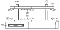
도 7은, 본 발명의 일 실시예에 따른 배터리 팩 기판 접속 시스템의 일부 구성을 개략적으로 나타내는 정면도이고, 도 8은, 본 발명의 일 실시예에 따른 고정 유닛의 일부 구성을 개략적으로 나타내는 평면도이다. 또한, 도 9는, 본 발명의 일 실시예에 따른 장착 유닛과 고정 유닛 사이에 배터리팩 기판이 장착된 구성을 개략적으로 나타내는 정면도이다. 또한, 본 실시예에서는, 앞선 실시예에 대한 설명이 유사하게 적용될 수 있는 부분에 대해서는 상세한 설명을 생략하고, 차이점이 있는 부분을 위주로 설명하도록 한다.FIG. 7 is a front view schematically showing some components of a battery pack board connection system according to an embodiment of the present invention, and FIG. 8 is a plan view schematically showing some components of a fixing unit according to an embodiment of the present invention. . 9 is a front view schematically illustrating a configuration in which a battery pack substrate is mounted between a mounting unit and a fixing unit according to an embodiment of the present invention. In addition, in the present embodiment, a detailed description of parts to which the description of the above embodiments may be similarly applied will be omitted, and description will be given focusing on differences.
도 1 및 도 7을 참조하면, 본 발명의 일 실시예에 따른 단자 접촉 유닛(110)은, 상부 방향으로 돌출 연장된 형태로 장착 유닛(100)에 구비될 수 있다. 예를 들어, 도 7의 구성에 도시된 바와 같이, 단자 접촉 유닛(110)은, 장착 유닛(100)의 일면에 구비될 수 있다. 보다 구체적으로, 단자 접촉 유닛(110)은, 장착 유닛(100)의 상부 표면에 장착될 수 있다. 또한, 단자 접촉 유닛(110)은, 장착 유닛(100)으로부터 상부 방향으로 돌출 연장된 형태로 장착 유닛에 구비될 수 있다.1 and 7, the
바람직하게는, 본 발명의 일 실시예에 따른 배터리 팩 기판 접속 시스템은, 도 7의 구성에 도시된 바와 같이, 고정 유닛(300)을 더 포함할 수 있다.Preferably, the battery pack board connection system according to an embodiment of the present invention may further include a fixing
상기 고정 유닛(300)은, 장착 유닛(100)과 소정 거리 이격되어 이격 공간에 보드가 개재될 수 있도록 구성될 수 있다. 예를 들어, 도 7의 구성에 도시된 바와 같이, 고정 유닛(300)은, 지지대(400)를 사이에 두고 장착 유닛(100)과 소정 거리 이격될 수 있다. 이 경우, 고정 유닛(300) 및 장착 유닛(100)에는 지지대(400)가 장착될 수 있도록 홀이 형성될 수 있다. The fixing
또한, 고정 유닛(300)은, 장착 유닛(100) 방향 및 반대 방향으로 양방향 이동 가능하도록 구성될 수 있다. 예를 들어, 고정 유닛(300)은, 지지대(400)에 의하여 상하 방향으로 이동할 수 있다. 이 경우, 지지대(400)는, 고정 유닛(300)을 상하 방향으로 이동시킬 수 있도록 동력 장치를 구비할 수 있다.In addition, the fixing
더욱 바람직하게는, 단자 접촉 유닛(310)은, 하부 방향으로 돌출 연장된 형태로 고정 유닛(300)에 구비될 수 있다. 예를 들어, 도 7의 구성에 도시된 바와 같이, 단자 접촉 유닛(310)은, 고정 유닛(300)의 일면에 구비될 수 있다. 보다 구체적으로, 단자 접촉 유닛(310)은, 고정 유닛(300)의 하부 표면에 장착될 수 있다. 또한, 단자 접촉 유닛(310)은, 고정 유닛(300)으로부터 하부 방향으로 돌출 연장된 형태로 고정 유닛(300)에 구비될 수 있다.More preferably, the
바람직하게는, 단자 접촉 유닛(110, 310)은, 도 7의 구성에 도시된 바와 같이, 고정 유닛(300)과 장착 유닛(100)에 각각 구비되어 서로를 향하는 방향으로 돌출 연장된 형태로 구성될 수 있다.Preferably, the terminal contact unit (110, 310), as shown in the configuration of Figure 7, each of which is provided in the fixed
또한, 단자 접촉 유닛(110, 310)은, 복수의 핀(111, 311)을 포함할 수 있다.In addition, the
상기 복수의 핀(111, 311)은, 복수의 단자(23)에 대응하는 위치에 장착되어 복수의 단자(23)에 전기적으로 접촉할 수 있도록 구성될 수 있다. 예를 들어, 도 3 및 도 7을 참조하면, 복수의 핀(111, 311)은, 보드(20)가 장착 유닛(100)에 장착 되고 고정 유닛(300)이 장착 유닛(100) 방향으로 이동하여 단자 접촉 유닛(110, 310)과 보드(20)가 접촉되는 경우, 복수의 단자(23)에 전기적으로 접촉 가능하도록 복수의 단자(23)에 대응하는 위치에 배치될 수 있다.The plurality of
바람직하게는, 장착 유닛(100) 및 고정 유닛(300)은, 보드(20)를 사이에 두고 서로 마주보는 위치에 단자 접촉 유닛(110, 310)이 각각 장착될 수 있다. 예를 들어, 도 7의 구성에 도시된 바와 같이, 장착 유닛(100)에 구비된 단자 접촉 유닛(110)과 고정 유닛(300)에 구비된 단자 접촉 유닛(310)은 상하 방향으로 서로 마주보는 위치에 배치될 수 있다.Preferably, the mounting
이와 같은 구성을 통해 본 발명의 일 실시예에 따른 단자 접촉 유닛(110, 310))은, 상하 방향으로 양쪽에서 보드(20)에 압력을 가하여 복수의 핀(111, 311)이 복수의 단자(23)에 전기적으로 용이하게 접촉할 수 있도록 할 수 있다.Through such a configuration, the
도 5 및 도 7을 참조하면, 본 발명의 일 실시예에 따른 복수의 핀(111, 311)은, 복수의 단자(23) 중 마이크로 컨트롤러(10)의 접속핀(11)과 전기적으로 연결된 단자(23_a)와 전기적으로 연결될 수 있도록 구성될 수 있다. 예를 들어, 도 4 및 도 7의 구성에 도시된 바와 같이, 복수의 핀(111, 311)은, 마이크로 컨트롤러(10)의 접속핀(11)과 전기적으로 연결된 제1 단자(23_a)와 전기적으로 연결될 수 있도록 제1 단자(23_a)에 대응하는 위치에 배치될 수 있다.5 and 7, a plurality of
도 5 및 도 8을 참조하면, 본 발명의 일 실시예에 따른 단자 접촉 유닛(310)은, 복수의 핀(311) 중 적어도 하나 이상의 허수인 핀을 포함할 수 있다. 예를 들어, 단자 접촉 유닛(310)은, 도 8의 구성에 도시된 바와 같이, 제1 핀(311_a) 및 제2 핀(311_b)을 포함할 수 있다. 예를 들어, 제1 핀(311_a)은, 제1 단자(23_a)와 전기적으로 연결될 수 있도록 제1 단자(23_a)에 대응하는 위치에 배치될 수 있다. 또한, 제2 핀(311_b)은, 제2 단자(23_b)와 전기적으로 연결될 수 있도록 제2 단자(23_b)에 대응하는 위치에 배치될 수 있다. 이 경우, 제1 단자(23_a)는, 마이크로 컨트롤러(10)의 접속핀(11)과 전기적으로 연결되고, 제2 단자(23_b)는, 마이크로 컨트롤러(10)의 접속핀(11)과 전기적으로 연결되지 않을 수 있다. 따라서, 제2 핀(311_b)은, 마이크로 컨트롤러(10)의 접속핀(11)과 연결되지 않는 허수인 핀일 수 있다.5 and 8, the
또한, 단자 접촉 유닛(310)은, 복수의 핀(311)의 위치를 단자 접촉 유닛(310)의 표면을 따라 이동 가능하도록 구성될 수 있다. 예를 들어, 도 8의 구성에서, 단자 접촉 유닛(310)은, 제1 핀(311_a) 및 제2 핀(311_b)의 위치를 단자 접촉 유닛(310)의 표면을 따라 수평방향으로 이동 가능하도록 구성될 수 있다. 이와 같은 구성을 통해 본 발명의 일 실시예에 따른 단자 접촉 유닛(310)은, 제1 핀(311_a) 및 제2 핀(311_b)과 대응되는 제1 단자(23_a) 및 제2 단자(23_b)의 위치에 따라서 제1 핀(311_a) 및 제2 핀(311_b)의 배치 위치를 이동시킬 수 있다.In addition, the
도 8 및 도 9를 참조하면, 본 발명의 일 실시예에 따른 고정 유닛(300)은, 고정캡(330)을 포함할 수 있다.8 and 9, the fixing
상기 고정캡(330)은, 단자 접촉 유닛(110, 310)이 상기 보드(20)에 접촉되는 경우, 보드(20)를 고정시킬 수 있도록 상하 방향으로 돌출되게 형성될 수 있다. 예를 들어, 도 9의 구성에 도시된 바와 같이, 고정캡(330)은, 고정 유닛(300)이 장착 유닛(100)의 방향으로 이동 및 가압하여 단자 접촉 유닛(110, 310)에 배치된 복수의 핀(111, 311)이 복수의 단자(23)에 접촉되는 경우, 복수의 핀(111, 311)과 복수의 단자(23)가 용이하게 접촉될 수 있도록 보드(20)를 고정시킬 수 있다.The fixing
또한, 고정캡(330)은, 고정 유닛(300)의 모서리부에 각각 위치될 수 있다. 예를 들어, 도 8 및 도 9의 구성에 도시된 바와 같이, 고정캡(330)은, 고정 유닛(300)의 4개의 모서리부에 각각 위치될 수 있다. 이와 같은 구성을 통해, 본 발명의 일 실시예에 따른 고정캡(330)은, 안정적으로 보드(20)를 고정시킬 수 있다.In addition, the fixing
도 7 및 도 9를 참조하면, 본 발명의 일 실시예에 따른 단자 접촉 유닛(110, 310)은, 고정 유닛(300)과 장착 유닛(100)에 각각 구비되어 서로를 향하는 방향으로 돌출 연장된 형태로 구성될 수 있다. 또한, 단자 접촉 유닛(110, 310)은, 복수의 핀(111, 311)을 포함할 수 있다. 또한, 복수의 핀(111, 311)은, 복수의 단자(23)에 대응하는 위치에 장착되어 복수의 단자(23)에 전기적으로 접촉할 수 있도록 구성될 수 있다. 이와 같은 구성을 통해, 본 발명의 일 실시예에 따른 단자 접촉 유닛(110, 310)은, 복수의 핀(111, 311)이 양방향에서 복수의 단자(23)에 압력을 가할 수 있도록 하여 복수의 핀(111, 311)과 복수의 단자(23)가 용이하게 접촉될 수 있도록 할 수 있다.7 and 9, the
한편, 본 명세서에서는 상, 하, 좌, 우, 전, 후와 같은 방향을 나타내는 용어가 사용되었으나, 이러한 용어들은 설명의 편의를 위한 것일 뿐, 대상이 되는 사물의 위치나 관측자의 위치 등에 따라 달라질 수 있음은 본 발명의 당업자에게 자명하다.In the present specification, terms indicating directions such as up, down, left, right, before, and after are used, but these terms are merely for convenience of description and may vary depending on the location of the object or the location of the observer. It will be apparent to those skilled in the art that the present invention can be made.
이상과 같이, 본 발명은 비록 한정된 실시예와 도면에 의해 설명되었으나, 본 발명은 이것에 의해 한정되지 않으며 본 발명이 속하는 기술분야에서 통상의 지식을 가진 자에 의해 본 발명의 기술사상과 아래에 기재될 특허청구범위의 균등범위 내에서 다양한 수정 및 변형이 가능함은 물론이다.As described above, although the present invention has been described by way of limited embodiments and drawings, the present invention is not limited thereto and is intended by those skilled in the art to which the present invention pertains. Of course, various modifications and variations are possible within the scope of equivalents of the claims to be described.
10: 마이크로 컨트롤러
11: 접속핀
20: 보드
21: 홈
23: 단자
24: 커넥터
25: 신호 경로
30: 연결 선로
31: 커넥터
100: 장착 유닛
110: 단자 접촉 유닛
111: 핀
130: 체결부
200: 연결 유닛
300: 고정 유닛
310: 단자 접촉 유닛
311: 핀
330: 고정캡
400: 지지대10: microcontroller
11: connecting pin
20: board
21: home
23: terminal
24: connector
25: signal path
30: connecting line
31: connector
100: mounting unit
110: terminal contact unit
111: pin
130: fastening part
200: connection unit
300: fixed unit
310: terminal contact unit
311: pin
330: fixed cap
400: support
Claims (12)
판상으로 구성되며, 상기 마이크로 컨트롤러가 적어도 일면에 장착되고, 적어도 일면에 복수의 홈이 형성된 보드;
전도성 재질로 이루어지고, 상기 복수의 홈에 각각 필링 되도록 구성된 복수의 단자; 및
상기 보드에 실장되고, 상기 복수의 단자와 상기 마이크로 컨트롤러 사이를 전기적으로 연결하도록 구성된 신호 경로
를 포함하는 것을 특징으로 하는 배터리 팩 기판.
Microcontroller;
A board having a plate shape, the microcontroller mounted on at least one surface thereof, and having a plurality of grooves formed on at least one surface thereof;
A plurality of terminals made of a conductive material and configured to be respectively filled in the plurality of grooves; And
A signal path mounted on the board and configured to electrically connect between the plurality of terminals and the microcontroller
Battery pack substrate comprising a.
상기 복수의 단자는, 제1 단자 및 제2 단자를 포함하며,
상기 제1 단자는, 상기 마이크로 컨트롤러의 접속핀과 전기적으로 연결되도록 구성되고,
상기 제2 단자는, 상기 마이크로 컨트롤러와 전기적으로 연결되지 않도록 구성된 것을 특징으로 하는 배터리 팩 기판.
The method of claim 1,
The plurality of terminals include a first terminal and a second terminal,
The first terminal is configured to be electrically connected to the connecting pin of the microcontroller,
And the second terminal is configured not to be electrically connected to the microcontroller.
상기 복수의 홈은, 상기 제1 단자가 필링된 제1 홈 및 상기 제2 단자가 필링된 제2 홈을 포함하며,
상기 제1 홈 및 상기 제2 홈은, 각각 복수개 구비되고,
상기 복수의 홈은, 적어도 하나의 상기 제2 홈이 적어도 2개의 상기 제1 홈 사이에 배치된 것을 특징으로 하는 배터리 팩 기판.
The method of claim 2,
The plurality of grooves may include a first groove filled with the first terminal and a second groove filled with the second terminal,
The first groove and the second groove are each provided in plural,
The plurality of grooves, the battery pack substrate, characterized in that at least one second groove is disposed between the at least two first grooves.
상기 복수의 홈은, 3개 이상의 상기 제1 홈이 서로 연결되어 이루는 다각형 내부에 적어도 하나의 상기 제2 홈이 포함되도록 배치된 것을 특징으로 하는 배터리 팩 기판.
The method of claim 3,
The plurality of grooves, the battery pack substrate, characterized in that arranged in such a way that at least one of the second grooves are included in the polygon formed by connecting the three or more first grooves.
상기 복수의 홈은, 상기 보드의 양면에 각각 형성되는 것을 특징으로 하는 배터리 팩 기판.
The method of claim 1,
The plurality of grooves are formed on both sides of the board, the battery pack substrate, characterized in that.
상기 복수의 단자는, 상기 복수의 홈의 깊이 방향으로 상기 복수의 홈의 깊이 보다 낮은 높이로 각각 충진되는 것을 특징으로 하는 배터리 팩 기판.
The method of claim 1,
The plurality of terminals are respectively filled in the depth direction of the plurality of grooves to a height lower than the depth of the plurality of grooves.
판상으로 구성되며, 상기 마이크로 컨트롤러가 적어도 일면에 장착되고, 적어도 일면에 복수의 홈이 형성된 보드와,
전도성 재질로 이루어지고, 상기 복수의 홈에 각각 필링 되도록 구성된 복수의 단자와,
상기 보드에 실장되고, 상기 복수의 단자와 상기 마이크로 컨트롤러 사이를 전기적으로 연결하도록 구성된 신호 경로를 포함하는 배터리 팩 기판;
상부에 상기 보드가 장착될 수 있도록 구성된 장착 유닛;
상하 방향으로 길게 연장된 부분이 형성된 복수의 핀을 구비하여 상기 복수의 단자에 전기적으로 접촉할 수 있도록 구성된 단자 접촉 유닛; 및
상기 단자 접촉 유닛과 전기적으로 연결되며, 외부 장치와 연결 가능하도록 구성된 연결 유닛
을 포함하는 것을 특징으로 하는 배터리 팩 기판 접속 시스템.
With microcontroller,
A board having a plate shape, the microcontroller mounted on at least one surface, and having a plurality of grooves formed on at least one surface thereof;
A plurality of terminals made of a conductive material and configured to be respectively filled in the plurality of grooves;
A battery pack substrate mounted on the board and including a signal path configured to electrically connect between the plurality of terminals and the microcontroller;
A mounting unit configured to mount the board thereon;
A terminal contact unit having a plurality of pins extending in a vertical direction and configured to be in electrical contact with the plurality of terminals; And
A connection unit electrically connected to the terminal contact unit and configured to be connectable to an external device
Battery pack substrate connection system comprising a.
상기 장착 유닛과 소정 거리 이격되어 이격 공간에 상기 보드가 개재될 수 있도록 구성되고, 상기 장착 유닛 방향 및 반대 방향으로 양방향 이동 가능하도록 구성된 고정 유닛
을 더 포함하는 것을 특징으로 하는 배터리 팩 기판 접속 시스템.
The method of claim 7, wherein
The fixed unit is configured so that the board is interposed in a spaced space spaced apart from the mounting unit by a predetermined distance, and configured to be bidirectionally moved in the opposite direction to the mounting unit
Battery pack substrate connection system further comprising.
상기 단자 접촉 유닛은, 상기 고정 유닛과 상기 장착 유닛에 각각 구비되어 서로를 향하는 방향으로 돌출 연장된 형태로 구성되며, 상기 복수의 단자에 대응하는 위치에 장착되어 상기 복수의 단자에 전기적으로 접촉할 수 있도록 구성된 복수의 핀을 포함하는 것을 특징으로 하는 배터리 팩 기판 접속 시스템.
The method of claim 8,
The terminal contact unit is provided in the fixed unit and the mounting unit, respectively, and configured to protrude in a direction facing each other, and is mounted at a position corresponding to the plurality of terminals to electrically contact the plurality of terminals. A battery pack board connection system comprising a plurality of pins configured to be capable of being connected to one another.
상기 복수의 단자는, 제1 단자 및 제2 단자를 포함하며,
상기 제1 단자는, 상기 마이크로 컨트롤러의 접속핀과 전기적으로 연결되도록 구성되고,
상기 제2 단자는, 상기 마이크로 컨트롤러와 전기적으로 연결되지 않도록 구성된 것을 특징으로 하는 배터리 팩 기판 접속 시스템.
The method of claim 9,
The plurality of terminals include a first terminal and a second terminal,
The first terminal is configured to be electrically connected to the connecting pin of the microcontroller,
And the second terminal is configured not to be electrically connected to the microcontroller.
상기 복수의 홈은, 상기 제1 단자가 필링된 제1 홈 및 상기 제2 단자가 필링된 제2 홈을 포함하며,
상기 제1 홈 및 상기 제2 홈은, 각각 복수개 구비되고,
상기 복수의 홈은, 적어도 하나의 상기 제2 홈이 적어도 2개의 상기 제1 홈 사이에 배치된 것을 특징으로 하는 배터리 팩 기판 접속 시스템.
The method of claim 10,
The plurality of grooves may include a first groove filled with the first terminal and a second groove filled with the second terminal,
The first groove and the second groove are each provided in plural,
And the plurality of grooves are at least one of the second grooves disposed between at least two of the first grooves.
상기 복수의 홈은, 3개 이상의 상기 제1 홈이 서로 연결되어 이루는 다각형 내부에 적어도 하나의 상기 제2 홈이 포함되도록 배치된 것을 특징으로 하는 배터리 팩 기판 접속 시스템.The method of claim 11,
And the plurality of grooves are arranged such that at least one of the second grooves is included in a polygon in which three or more first grooves are connected to each other.
Priority Applications (1)
| Application Number | Priority Date | Filing Date | Title |
|---|---|---|---|
| KR1020180098860A KR102650086B1 (en) | 2018-08-23 | 2018-08-23 | Battery pack substrate and Battery pack substrate accessing system |
Applications Claiming Priority (1)
| Application Number | Priority Date | Filing Date | Title |
|---|---|---|---|
| KR1020180098860A KR102650086B1 (en) | 2018-08-23 | 2018-08-23 | Battery pack substrate and Battery pack substrate accessing system |
Publications (2)
| Publication Number | Publication Date |
|---|---|
| KR20200022792A true KR20200022792A (en) | 2020-03-04 |
| KR102650086B1 KR102650086B1 (en) | 2024-03-20 |
Family
ID=69783174
Family Applications (1)
| Application Number | Title | Priority Date | Filing Date |
|---|---|---|---|
| KR1020180098860A KR102650086B1 (en) | 2018-08-23 | 2018-08-23 | Battery pack substrate and Battery pack substrate accessing system |
Country Status (1)
| Country | Link |
|---|---|
| KR (1) | KR102650086B1 (en) |
Citations (4)
| Publication number | Priority date | Publication date | Assignee | Title |
|---|---|---|---|---|
| JP2003338668A (en) * | 2002-05-21 | 2003-11-28 | Fujikura Ltd | Circuit board, multilayer circuit board and manufacturing method therefor |
| WO2009028596A1 (en) * | 2007-08-30 | 2009-03-05 | Nec Corporation | Passive element built-in substrate, manufacturing method, and semiconductor device |
| KR20150106027A (en) * | 2014-03-10 | 2015-09-21 | 세방전지(주) | Battery pack for electric car and the control method thereof |
| KR20160015594A (en) * | 2014-07-31 | 2016-02-15 | 김홍민 | Electronic circuit construction device for improved reliability using conductive connection module |
-
2018
- 2018-08-23 KR KR1020180098860A patent/KR102650086B1/en active IP Right Grant
Patent Citations (4)
| Publication number | Priority date | Publication date | Assignee | Title |
|---|---|---|---|---|
| JP2003338668A (en) * | 2002-05-21 | 2003-11-28 | Fujikura Ltd | Circuit board, multilayer circuit board and manufacturing method therefor |
| WO2009028596A1 (en) * | 2007-08-30 | 2009-03-05 | Nec Corporation | Passive element built-in substrate, manufacturing method, and semiconductor device |
| KR20150106027A (en) * | 2014-03-10 | 2015-09-21 | 세방전지(주) | Battery pack for electric car and the control method thereof |
| KR20160015594A (en) * | 2014-07-31 | 2016-02-15 | 김홍민 | Electronic circuit construction device for improved reliability using conductive connection module |
Also Published As
| Publication number | Publication date |
|---|---|
| KR102650086B1 (en) | 2024-03-20 |
Similar Documents
| Publication | Publication Date | Title |
|---|---|---|
| US8936865B2 (en) | Bus bar holder and battery pack including the same | |
| US20040263117A1 (en) | Battery pack with built in communication port | |
| KR20220010575A (en) | Bettery module | |
| TW201947803A (en) | Battery module and car | |
| KR102395752B1 (en) | Battery pack | |
| JPH0794232A (en) | Electric connector for battery | |
| US11336039B2 (en) | Connector for printed circuit board and battery system comprising printed circuit board and connector | |
| KR20140093108A (en) | Battery pack | |
| KR102381962B1 (en) | Battery Pack Having Heat Dissipating Member | |
| US20200333194A1 (en) | Apparatus and Method for Measuring Temperature of Battery | |
| US11454676B2 (en) | Apparatus for estimating state of secondary battery, and battery pack including the same | |
| RU2009120368A (en) | BATTERY BLOCKS | |
| KR20210058540A (en) | Battery Rack | |
| JPH11297366A (en) | Battery pack, battery charger, and electrical equipment using the battery pack | |
| EP3316386B1 (en) | Connector part for a printed circuit board and a battery system comprising the printed circuit board and the connector part | |
| CN111133321B (en) | Shunt resistor and apparatus for detecting current including the same | |
| KR102337901B1 (en) | Printed Circuit Board Assembly and Method for Manufacturing the Same | |
| KR102637979B1 (en) | Battery module | |
| KR102650086B1 (en) | Battery pack substrate and Battery pack substrate accessing system | |
| KR102649292B1 (en) | Apparatus for accessing battery pack substrate | |
| EP3671941A1 (en) | Secondary battery and battery pack comprising same | |
| US11705587B2 (en) | Terminal case having the improved function of estimating state of secondary battery | |
| CN211239404U (en) | Charging system | |
| CN109687201B (en) | Socket, plug and mobile terminal | |
| US20230139879A1 (en) | Battery pack including member capable of preventing poor contact with device |
Legal Events
| Date | Code | Title | Description |
|---|---|---|---|
| E902 | Notification of reason for refusal | ||
| E701 | Decision to grant or registration of patent right | ||
| GRNT | Written decision to grant |