KR20180098170A - Organic device for X-ray detect and method of manufacturing the same - Google Patents
Organic device for X-ray detect and method of manufacturing the same Download PDFInfo
- Publication number
- KR20180098170A KR20180098170A KR1020180022136A KR20180022136A KR20180098170A KR 20180098170 A KR20180098170 A KR 20180098170A KR 1020180022136 A KR1020180022136 A KR 1020180022136A KR 20180022136 A KR20180022136 A KR 20180022136A KR 20180098170 A KR20180098170 A KR 20180098170A
- Authority
- KR
- South Korea
- Prior art keywords
- pcbm
- layer
- pcdtbt
- active layer
- scintillator
- Prior art date
Links
Images


Classifications
-
- H—ELECTRICITY
- H10—SEMICONDUCTOR DEVICES; ELECTRIC SOLID-STATE DEVICES NOT OTHERWISE PROVIDED FOR
- H10K—ORGANIC ELECTRIC SOLID-STATE DEVICES
- H10K39/00—Integrated devices, or assemblies of multiple devices, comprising at least one organic radiation-sensitive element covered by group H10K30/00
- H10K39/30—Devices controlled by radiation
- H10K39/36—Devices specially adapted for detecting X-ray radiation
-
- H01L27/308—
-
- G—PHYSICS
- G01—MEASURING; TESTING
- G01T—MEASUREMENT OF NUCLEAR OR X-RADIATION
- G01T1/00—Measuring X-radiation, gamma radiation, corpuscular radiation, or cosmic radiation
- G01T1/16—Measuring radiation intensity
- G01T1/24—Measuring radiation intensity with semiconductor detectors
-
- H01L51/4206—
-
- H—ELECTRICITY
- H10—SEMICONDUCTOR DEVICES; ELECTRIC SOLID-STATE DEVICES NOT OTHERWISE PROVIDED FOR
- H10K—ORGANIC ELECTRIC SOLID-STATE DEVICES
- H10K30/00—Organic devices sensitive to infrared radiation, light, electromagnetic radiation of shorter wavelength or corpuscular radiation
- H10K30/451—Organic devices sensitive to infrared radiation, light, electromagnetic radiation of shorter wavelength or corpuscular radiation comprising a metal-semiconductor-metal [m-s-m] structure
-
- Y—GENERAL TAGGING OF NEW TECHNOLOGICAL DEVELOPMENTS; GENERAL TAGGING OF CROSS-SECTIONAL TECHNOLOGIES SPANNING OVER SEVERAL SECTIONS OF THE IPC; TECHNICAL SUBJECTS COVERED BY FORMER USPC CROSS-REFERENCE ART COLLECTIONS [XRACs] AND DIGESTS
- Y02—TECHNOLOGIES OR APPLICATIONS FOR MITIGATION OR ADAPTATION AGAINST CLIMATE CHANGE
- Y02E—REDUCTION OF GREENHOUSE GAS [GHG] EMISSIONS, RELATED TO ENERGY GENERATION, TRANSMISSION OR DISTRIBUTION
- Y02E10/00—Energy generation through renewable energy sources
- Y02E10/50—Photovoltaic [PV] energy
- Y02E10/549—Organic PV cells
-
- Y—GENERAL TAGGING OF NEW TECHNOLOGICAL DEVELOPMENTS; GENERAL TAGGING OF CROSS-SECTIONAL TECHNOLOGIES SPANNING OVER SEVERAL SECTIONS OF THE IPC; TECHNICAL SUBJECTS COVERED BY FORMER USPC CROSS-REFERENCE ART COLLECTIONS [XRACs] AND DIGESTS
- Y02—TECHNOLOGIES OR APPLICATIONS FOR MITIGATION OR ADAPTATION AGAINST CLIMATE CHANGE
- Y02P—CLIMATE CHANGE MITIGATION TECHNOLOGIES IN THE PRODUCTION OR PROCESSING OF GOODS
- Y02P70/00—Climate change mitigation technologies in the production process for final industrial or consumer products
- Y02P70/50—Manufacturing or production processes characterised by the final manufactured product
Landscapes
- Physics & Mathematics (AREA)
- Health & Medical Sciences (AREA)
- Life Sciences & Earth Sciences (AREA)
- General Physics & Mathematics (AREA)
- High Energy & Nuclear Physics (AREA)
- Molecular Biology (AREA)
- Spectroscopy & Molecular Physics (AREA)
- Electromagnetism (AREA)
- Measurement Of Radiation (AREA)
Abstract
Description
본 발명은 X-선 검출용 유기소자 및 그 제조방법에 관한 것으로, 더욱 상세하게는 PCDTBT:PCBM을 이용한 X-선 검출용 유기소자 및 그 제조방법에 관한 것이다.The present invention relates to an organic device for X-ray detection and a method of manufacturing the same, and more particularly, to an organic device for X-ray detection using PCDTBT: PCBM and a method of manufacturing the same.
일반적으로, 사용빈도가 높은 디지털 X-선 영상장치는 크게 광도전체 (photoconductor)의 전기적 신호를 직접 받아 영상을 만들어내는 직접변환방식과 유도된 섬광체(scintillator)의 빛을 집광 소자를 이용하여 전기신호로 변환시켜 영상을 만들어내는 간접변환방식이 있다.Generally, a digital X-ray imaging apparatus having a high frequency of use generally includes a direct conversion system that directly receives an electrical signal of a photoconductor to generate an image, and a direct conversion system that converts an induced scintillator light into an electrical signal And an indirect conversion method in which an image is generated.
종래에는 반도체 무기재료 기반의 X-선 검출기가 일반적으로 사용되고 있으며 대체할 기술로써 유기태양전지 기술과 X-선 기술을 접목시킨 유기재료 기반의 검출소자의 연구가 진행되고 있다.Conventionally, an X-ray detector based on a semiconductor inorganic material is generally used, and as an alternative technology, an organic material-based detection element that combines organic solar cell technology and X-ray technology is being studied.
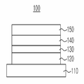
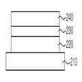
도 1은 종래의 X-선 검출용 유기소자를 나타내는 도면이다.1 is a view showing a conventional organic device for X-ray detection.
도 1을 참조하면, 종래의 X-선 검출용 유기소자(100)는 기판(110), 기판(110) 상부에 형성되는 제1 전극층(120), 제1 전극층(120) 상부에 형성되고 정공의 수송을 향상시키는 정공수송층(130), 정공수송층(130) 상부에 형성되고 인가되는 X-선으로부터 전자-정공쌍을 형성하는 활성층(140) 및 활성층(140) 상부에 형성되는 제2 전극층(150)을 포함한다.Referring to FIG. 1, a conventional organic
이러한 종래의 X-선 검출용 유기소자(100)의 경우 1V 이하의 구동전압에서 동작하며, X-선이 인가되었을 때 변환효율은 반도체기반 검출기의 100분의 1정도의 검출 성능을 갖는다.The conventional organic
또한, 종래의 X-선 검출용 유기소자(100)는 활성층(140) 물질로써 일반적으로 P3HT:PCBM을 사용한다. 하지만, 간접변환방식에 있어서 P3HT:PCBM 활성층(140)이 적용된 검출소자의 경우 섬광체에서 변환되어 도달하는 광을 다시 전기신호로 변환하는 검출 효율이 낮기에 이에 대한 개선이 필요하다.In addition, the conventional organic
본 발명은 상술한 종래 기술의 문제점을 해결하기 위한 것이다. 즉, 종래의 물질 대비 우수한 흡광도를 기반으로 신호 취득 효율을 향상시킬 수 있는 X-선 검출용 유기소자 및 그 제조방법을 제공함에 있다.SUMMARY OF THE INVENTION The present invention has been made to solve the above problems of the prior art. That is, an object of the present invention is to provide an organic device for X-ray detection capable of improving signal acquisition efficiency based on an excellent absorbance compared to a conventional material, and a method of manufacturing the same.
상기 과제를 해결하기 위한 본 발명의 X-선 검출용 유기소자는 기판, 상기 기판 상부에 형성되는 제1 전극층, 상기 제1 전극층 상부에 형성되고, 정공의 수송을 향상시키는 정공수송층, 상기 정공수송층 상부에 형성되고, 상기 기판 하부에서 발생한 가시광선을 흡수하여 전자-정공 쌍을 생성하는 활성층, 상기 활성층 상부에 형성되는 제2 전극층 및 상기 기판 하부에 형성되며, X-선을 가시광선으로 변환하는 섬광체층(scintillator)을 포함하고, 상기 활성층은 PCDTBT:PCBM의 혼합물로 형성되는 것을 특징으로 한다.According to an aspect of the present invention, there is provided an organic device for X-ray detection comprising a substrate, a first electrode layer formed on the substrate, a hole transport layer formed on the first electrode layer to improve transport of holes, A second electrode layer formed on the active layer, and a second electrode layer formed under the substrate, the first electrode layer being formed on the upper surface of the active layer, And a scintillator, wherein the active layer is formed of a mixture of PCDTBT: PCBM.
상기 PCDTBT:PCBM는 상기 PCDTBT 1중량부에 대하여 PCBM 2 내지 4.5중량부로 이루어질 수 있다.The PCDTBT: PCBM may be composed of 2 to 4.5 parts by weight of PCBM per 1 part by weight of the PCDTBT.
상기 PCDTBT:PCBM는 상기 섬광체층의 스팩트럼 특성과 비교하여 높은 정합도를 갖도록 PCDTBT 1중량부에 대하여 PCBM 4중량부를 갖을 수 있다.The PCDTBT: PCBM may have 4 parts by weight of PCBM relative to 1 part by weight of PCDTBT so as to have a high degree of matching as compared with the spectral characteristics of the scintillator layer.
상기 PCDTBT:PCBM이 혼합된 상기 활성층은 65nm 내지 90nm의 두께를 갖을 수 있다.The active layer in which the PCDTBT: PCBM is mixed may have a thickness of 65 nm to 90 nm.
상기 PCDTBT:PCBM이 혼합된 상기 활성층은 85nm의 두께를 갖을 수 있다.The active layer in which the PCDTBT: PCBM is mixed may have a thickness of 85 nm.
상기 섬광체층은 Nal:TI, Csl:TI, Y3Al5O12:Ce, CdWO4, LuAG:Ce및 Gd2O2S:Tb로 이루어진 군에서 어느 하나로 형성될 수 있다.The scintillator layer may be formed of any one of the group consisting of Nal: TI, CsI: TI, Y3Al5O12: Ce, CdWO4, LuAG: Ce and Gd2O2S: Tb.
상기 Csl:TI 물질로 형성된 섬광체층의 발광도와 상기 PCDTBT:PCBM이 혼합된 활성층의 흡광도가 500 내지 650nm 파장 영역에서 겹칠 수 있다.The luminescence of the scintillator layer formed of the Csl: TI material and the absorbance of the active layer mixed with the PCDTBT: PCBM may overlap in the wavelength range of 500 to 650 nm.
상기 섬광체층은 1mm이하의 두께를 갖을 수 있다.The scintillator layer may have a thickness of 1 mm or less.
상기 과제를 해결하기 위한 본 발명의 X-선 검출용 유기소자의 제조방법은 기판 상부에 제1 전극층을 형성하는 단계, 상기 제1 전극층 상부에 정공수송층을 형성하는 단계, 상기 정공수송층 상부에 PCDTBT:PCBM의 혼합물로 형성된 활성층을 형성하는 단계, 상기 활성층 상부에 제2 전극층을 형성하는 단계 및 상기 기판 하부에 섬광체층(scintillator)을 형성하는 단계를 포함한다.According to another aspect of the present invention, there is provided a method of manufacturing an organic device for X-ray detection, comprising: forming a first electrode layer on a substrate; forming a hole transport layer on the first electrode layer; : Forming an active layer formed of a mixture of PCBM, forming a second electrode layer on the active layer, and forming a scintillator under the substrate.
상기 기판 상부에 제1 전극층을 형성하는 단계에서, 상기 기판은 ITO 투명 전극이 코팅된 무알칼리 글라스(Non-Alkali Glass) 기판일 수 있다.In the step of forming the first electrode layer on the substrate, the substrate may be a non-alkali glass substrate coated with an ITO transparent electrode.
상기 활성층을 형성하는 단계에서, 상기 PCDTBT:PCBM는 상기 PCDTBT 1중량부에 대하여 PCBM 2 내지 4.5중량부로 이루어질 수 있다.In the step of forming the active layer, the PCDTBT: PCBM may be composed of 2 to 4.5 parts by weight of PCBM per 1 part by weight of the PCDTBT.
상기 활성층을 형성하는 단계에서, 상기 PCDTBT:PCBM이 혼합된 상기 활성층은 65nm 내지 90nm의 두께를 갖을 수 있다.In the step of forming the active layer, the active layer in which the PCDTBT: PCBM is mixed may have a thickness of 65 nm to 90 nm.
상기 섬광체층을 형성하는 단계에서, 상기 섬광체층은 Nal:TI, Csl:TI, Y3Al5O12:Ce, CdWO4, LuAG:Ce및 Gd2O2S:Tb로 이루어진 군에서 어느 하나로 형성될 수 있다.In the step of forming the scintillator layer, the scintillator layer may be formed of one selected from the group consisting of Nal: TI, CsI: TI, Y3Al5O12: Ce, CdWO4, LuAG: Ce and Gd2O2S: Tb.
상기 Csl:TI 물질로 형성된 섬광체층의 발광도와 상기 PCDTBT:PCBM이 혼합된 활성층의 흡광도가 500 내지 650nm 파장 영역에서 겹칠 수 있다.The luminescence of the scintillator layer formed of the Csl: TI material and the absorbance of the active layer mixed with the PCDTBT: PCBM may overlap in the wavelength range of 500 to 650 nm.
상기 제2 전극층을 형성하는 단계 이후에 봉지(Encapsulation)공정을 수행하는 단계를 더 포함할 수 있다.And performing an encapsulation process after forming the second electrode layer.
본 발명에 따르면, 간접변환방식의 유기재료 기반의 X-선 검출소자를 제작함으로써 종래의 반도체기반의 검출소자보다 대면적, 경제성, 공정적인 부분 등의 측면에서 장점을 갖고 있다.According to the present invention, by manufacturing an X-ray detecting element based on an organic material of indirect conversion type, it has advantages in terms of area, economical efficiency, and process part compared with the conventional semiconductor-based detecting element.
즉, 종래의 P3HT:PCBM의 혼합물질을 기반으로 한 활성층을 포함하는 X-선 검출소자의 경우 가시광 영역의 흡광도가 저조하여 조사된 X-선이 섬광체에 의해 빛으로 변환되어 검출소자에 입사될 경우 그 흡수율이 낮은 단점을 가지고 있으나, 본 발명에 따른 PCDTBT:PCBM 혼합물질을 기반으로 한 활성층을 포함하는 X-선 검출소자의 경우 종래의 P3HT:PCBM 대비 가시광 영역의 흡광도가 우수하여 신호 취득 효율을 향상시킬 수 있는 장점이 있다.That is, in the case of an X-ray detecting element including an active layer based on a conventional P3HT: PCBM mixed material, the X-ray irradiated due to low absorbance in the visible light region is converted into light by the scintillator, However, in the case of the X-ray detecting device including the active layer based on the PCDTBT: PCBM mixed material according to the present invention, the absorbance of the visible light region is superior to that of the conventional P3HT: PCBM, There is an advantage that it can be improved.
본 발명의 기술적 효과들은 이상에서 언급한 것들로 제한되지 않으며, 언급되지 않은 또 다른 기술적 효과들은 아래의 기재로부터 당업자에게 명확하게 이해될 수 있을 것이다.The technical effects of the present invention are not limited to those mentioned above, and other technical effects not mentioned can be clearly understood by those skilled in the art from the following description.
도 1은 종래의 X-선 검출용 유기소자를 나타내는 도면이다.
도 2는 본 발명의 X-선 검출용 유기소자를 나타내는 도면이다.
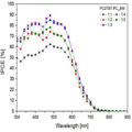
도 3은 X-선 검출용 유기소자의 두 가지 활성층 물질(P3HT:PCBM, PCDTBT:PCBM)의 흡광 곡선과 섬광체의 발광 곡선의 비교 그래프이다.
도 4 내지 도 8은 본 발명의 X-선 검출용 유기소자의 제작방법을 나타내는 도면이다.
도 9는 본 발명에 따른 X-선 검출소자의 X-선 노출시 검출된 전하량을 나타내는 그래프이다.
도 10은 본 발명의 PCDTBT:PCBM 혼합 비율에 따른 간접변환방식의 X-선 검출소자의 특성을 나타낸 그래프이다.
도 11은 본 발명의 PCDTBT:PCBM 혼합 비율에 따른 X-선 검출소자의 IPCE 특성을 나타낸 그래프이다.
도 12는 본 발명의 PCDTBT:PCBM이 혼합된 활성층의 두께에 따른 특성 변화를 나타내는 그래프이다.
도 13은 X-선 검출용 유기소자의 두 가지 활성층 물질(P3HT:PCBM, PCDTBT:PCBM)에 대한 민감도와 암 전류 밀도를 비교하기 위한 그래프이다.1 is a view showing a conventional organic device for X-ray detection.
2 is a view showing an organic device for X-ray detection of the present invention.
FIG. 3 is a graph showing a comparison of the extinction curves of the two active layer materials (P3HT: PCBM, PCDTBT: PCBM) of the organic device for X-ray detection and the emission curves of the scintillators.
Figs. 4 to 8 are views showing a method of manufacturing an organic device for X-ray detection of the present invention.
FIG. 9 is a graph showing the amount of charge detected by X-ray exposure of the X-ray detecting element according to the present invention.
10 is a graph showing the characteristics of the indirect conversion type X-ray detection device according to the PCDTBT: PCBM mixture ratio of the present invention.
11 is a graph showing IPCE characteristics of the X-ray detecting device according to the PCDTBT: PCBM mixing ratio of the present invention.
12 is a graph showing a change in the characteristics of the active layer mixed with PCDTBT: PCBM according to the thickness of the present invention.
FIG. 13 is a graph for comparing sensitivity and dark current density for two active layer materials (P3HT: PCBM, PCDTBT: PCBM) of an organic device for X-ray detection.
본 발명은 다양한 변환을 가할 수 있고 여러 가지 실시 예를 가질 수 있는바, 특정 실시 예들을 도면에 예시하고 상세한 설명에 상세하게 설명하고자 한다. 그러나, 이는 본 발명을 특정한 실시 형태에 대해 한정하려는 것이 아니며, 본 발명의 사상 및 기술 범위에 포함되는 모든 변환, 균등물 내지 대체물을 포함하는 것으로 이해되어야 한다. 본 발명을 설명함에 있어서 관련된 공지 기술에 대한 구체적인 설명이 본 발명의 요지를 흐릴 수 있다고 판단되는 경우 그 상세한 설명을 생략한다.BRIEF DESCRIPTION OF THE DRAWINGS The present invention is capable of various modifications and various embodiments, and specific embodiments are illustrated in the drawings and described in detail in the detailed description. It is to be understood, however, that the invention is not to be limited to the specific embodiments, but includes all modifications, equivalents, and alternatives falling within the spirit and scope of the invention. DETAILED DESCRIPTION OF THE PREFERRED EMBODIMENTS Hereinafter, the present invention will be described in detail with reference to the accompanying drawings.
이하, 본 발명에 따른 실시 예들을 첨부 도면을 참조하여 상세히 설명하기로 하며, 첨부 도면을 참조하여 설명함에 있어, 동일하거나 대응하는 구성 요소는 동일한 도면번호를 부여하고 이에 대한 중복되는 설명은 생략하기로 한다.DETAILED DESCRIPTION OF THE PREFERRED EMBODIMENTS Hereinafter, exemplary embodiments of the present invention will be described in detail with reference to the accompanying drawings. Referring to the accompanying drawings, the same or corresponding components are denoted by the same reference numerals, .
실시예Example
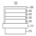
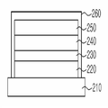
도 2는 본 발명의 X-선 검출용 유기소자(200)를 나타내는 도면이다.2 is a view showing an
도 2를 참조하면, 본 발명에 따른 X-선 검출용 유기소자(200)는 기판(210), 제1 전극층(220), 정공수송층(230), 활성층(240), 제2 전극층(250) 및 섬광체층(scintillator)(270)을 포함하며, 하부로부터 섬광체층(270), 기판(210), 제1 전극층(220), 정공수송층(230), 활성층(240) 및 제2 전극층(250)의 순서로 형성될 수 있다.2, an
기판(210)은 유리 또는 유연성이 있는 플라스틱으로 형성될 수 있다. 기판(210)이 유연성이 있는 플라스틱일 경우, PET(polyethylene terephthalate), PES (polyester), PT(polythiophene), PI(polyimide)중에서 어느 하나인 플라스틱으로 형성되거나, 알루미늄 포일(aluminum foil), 또는 스테인리스 스틸 포일(stainless steel foil)인 유연한 재료로 형성되어 유연성을 가진다. 바람직한 실시예에 따르면, 본 발명에 따른 기판(210)은 ITO 투명 전극이 코팅된 무알칼리 글라스(Non-Alkali Glass) 기판(210)일 수 있다.The
제1 전극층(220)은 기판(210) 상부에 형성될 수 있으며, 제1 전극층(220)은 투명하거나 전도성 물질일 수 있다. 제1 전극층(220)을 이루는 물질은 인듐 틴 옥사이드(indium tin oxide: ITO), 안티몬 틴 옥사이드(antimony tin oxide: ATO), 플루오린 틴 옥사이드(fluorine tin oxide: FTO), 알루미늄 도핑된 징크 옥사이드(Al-doped Zinc Oxide: AZO) 등으로 이루어진 군에서 선택된 1종 이상일 수 있다. 바람직하게는 인듐 틴 옥사이드(ITO)를 사용하여 제1 전극층(220)이 형성될 수 있다.The
정공수송층(230)은 제1 전극층(220) 상부에 형성될 수 있으며, 활성층(240)과 제1 전극층(220) 사이에 계면 특성을 개선하여 전하 전달 효율을 향상시킬 수 있다. 정공수송층(230)의 재료로는 정공을 수송하는 능력을 갖고, 전자를 차단하는 특성 뿐 아니라 박막 형성 능력이 우수한 화합물일 수 있다. 예를 들어, 정공수송층(230)의 재료는 TPD, PEDOT:PSS, G-PEDOT, PANI:PSS, PANI:CSA, PDBT, NPB, 아릴아민기(arylamine group)를 가지는 저분자와 고분자, 방향족아민기(aromatic amine group)를 가지는 저분자와 고분자 등일 수 있다. 정공수송층(230)의 형성방법으로는 스핀 코팅법, 스프레이 코팅법, 스크린 인쇄법, 바(bar) 코팅법, 닥터블레이드 코팅법, 그라비아 프린팅법 등이 적용될 수 있다.The
활성층(240)은 정공수송층(230) 상부에 형성될 수 있으며, 활성층(240)에서는 인가된 X-선으로부터의 전자와 정공이 각각의 전극으로 분리되어 수송 및 주입된다. 활성층(240)은 다양한 형태로 구현이 가능한데, 도너(donor)물질과 억셉터(acceptor)물질의 혼합박막층의 1층구조를 취할 수도 있으며, 도너물질과 억셉터 물질이 각각 적층된 형태의 2층구조를 취할 수도 있다.The
도너물질로는 CuPc(copper phthalocyanine)과 같은 프탈로 시아닌계 안료, 인디고, 티오인디고계 안료, 멜로시아닌 화합물, 시아닌 화합물 등의 저분자 화합물과 폴리파라페닐렌비닐렌(poly-ρ-phenylenevinylene; PPV)등과 같은 페닐렌비닐렌계 고분자 유도체, 폴리티오펜(polythiophene), PCPDTBT, P3HT등과 같은 싸이오펜계 고분자 유도체 등을 포함하는 전도성 고분자가 이용될 수 있으나, 본 발명에 따른 바람직한 실시예에 따르면 도너물질로 PCPDTBT가 사용될 수 있다.Examples of the donor material include low molecular weight compounds such as phthalocyanine pigments such as CuPc (copper phthalocyanine), indigo, thioindigo pigments, melocyanin compounds and cyanine compounds, and poly-ρ-phenylenevinylene (PPV ), Etc., and a thiophene-based polymer derivative such as polythiophene, PCPDTBT, P3HT, etc. may be used. According to a preferred embodiment of the present invention, the donor material PCPDTBT can be used.
억셉터 물질로는 풀러렌(fullerene; C60), ICBA, ICBM, PCBM, PC70BM과 같은 풀러렌 유도체, 페릴렌(perylene), PTCBI와 같은 페릴렌 유도체, CdS, CdSe, CdTe, 또는 ZnSe와 같은 반도체 나노입자가 사용 될 수 있으나, 본 발명에 따른 바람직한 실시예에 따르면 억셉터 물질로 PCBM이 사용될 수 있다.Examples of the acceptor material include fullerene derivatives such as fullerene (C60), ICBA, ICBM, PCBM and PC70BM, perylene derivatives such as perylene and PTCBI, semiconductor nanoparticles such as CdS, CdSe, CdTe, or ZnSe PCBM may be used as an acceptor material according to a preferred embodiment of the present invention.
즉, 본 발명에 따른 X-선 검출용 유기소자(200)의 활성층(240) 물질로써 도너물질인 PCPDTBT와 억셉터 물질인 PCBM를 혼합한 PCDTBT:PCBM 혼합물이 활성층(240)으로 사용될 수 있다. 일예로써, 종래의 P3HT:PCBM의 혼합물질을 기반으로 한 활성층(240)을 포함하는 유기 검출소자의 경우 가시광 영역의 흡광도가 저조하여 조사된 X-선이 섬광체에 의해 빛으로 변환되어 검출소자에 입사될 경우 그 흡수율이 낮은 단점을 가지고 있으나, 본 발명에 따른 PCDTBT:PCBM 혼합물질을 기반으로 한 활성층(240)을 포함하는 X-선 검출용 유기소자(200)의 경우 종래의 P3HT:PCBM 대비 가시광 영역의 흡광도가 우수하여 신호 취득 효율을 향상시킬 수 있는 장점이 있다.That is, a PCDTBT: PCBM mixture in which the donor material PCPDTBT and the acceptor material PCBM are mixed can be used as the
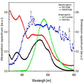
도 3은 X-선 검출용 유기소자의 두 가지 활성층 물질(P3HT:PCBM, PCDTBT:PCBM)의 흡광 곡선과 섬광체의 발광 곡선의 비교 그래프이다.FIG. 3 is a graph showing a comparison of the extinction curves of the two active layer materials (P3HT: PCBM, PCDTBT: PCBM) of the organic device for X-ray detection and the emission curves of the scintillators.
도 3을 참조하면, 간접변환방식의 유기재료 기반의 X-선 검출소자에 대해 종래의 활성층 물질인 P3HT:PCBM과 본 발명에 따른 활성층(240) 물질인 PCDTBT:PCBM의 발광 곡선을 섬광체(scintillator)의 발광 곡선과 비교하였다.Referring to FIG. 3, the emission curve of P3HT: PCBM, which is a conventional active layer material, and PCDTBT: PCBM, which is an
도 3에 도시한 그래프에서와 같이 종래의 P3HT:PCBM가 혼합된 활성층의 경우 약 520nm의 파장대역에서 흡광도(absorbance)가 최고치를 보인 이후 파장이 증가할수록 흡광도가 낮아지다가 600nm 중반 이후부터는 빛을 거의 흡수하지 못하는 양상을 보인다. 그러나, 본 발명의 PCDTBT:PCBM가 혼합된 활성층의 경우 전체 가시광 영역 대역에서 P3HT:PCBM에 비해 상대적으로 우수한 흡광도를 보이며, 특히, CsI(Tl) 섬광체의 발광 곡선을 고려할 경우 피크 레벨 560nm 대비 56% 감소한 영역인 500nm ~ 650nm 영역에서 정합도가 높기 때문에 많은 빛의 흡수로 전류 발생에 우수한 특성을 보인다.As shown in the graph of FIG. 3, in the case of the active layer mixed with the conventional P3HT: PCBM, the absorbance at the wavelength band of about 520 nm is the highest, and then the absorbance decreases as the wavelength increases. It does not absorb. However, in the case of the active layer mixed with PCDTBT: PCBM according to the present invention, the absorbance is relatively higher than that of P3HT: PCBM in the whole visible light region band. In particular, when the emission curve of the CsI (Tl) It shows excellent characteristics in current generation due to high absorption of light due to high matching degree in the region of 500 nm to 650 nm which is a reduced region.
또한, PCDTBT:PCBM의 혼합 비율은 PCDTBT 1중량부에 대하여 PCBM 2 내지 4.5중량부로 이루어지는 것이 바람직하다. 더욱 상세하게는, PCDTBT:PCBM는 섬광체의 스팩트럼 특성과 비교하여 높은 정합도를 갖도록 PCDTBT와 PCBM의 중량비율로 1:4를 갖는 것이 바람직하다.The mixing ratio of PCDTBT: PCBM is preferably 2 to 4.5 parts by weight of PCBM per 1 part by weight of PCDTBT. More specifically, it is preferable that PCDTBT: PCBM has 1: 4 by weight ratio of PCDTBT and PCBM so as to have a high matching degree in comparison with the spectral characteristics of the scintillator.
만약, PCDTBT 1중량부에 대하여 PCBM 2중량부 이하가 되면, 수집 전류 밀도(Collected CurrentDensity, CCD)가 낮아지기 때문에 검출감도가 혼합 비율 1:4 대비 8%이상 급격히 감소하며, 혼합 비율이 1:1에서는 검출감도가 38%나 감소되는 경향을 보인다. 또한, PCDTBT 1중량부에 대하여 PCBM 4.5중량부 이상이 되면, 암 전류 밀도(Dark CurrentDensity, DCD)의 증가와 수집 전류 밀도의 감소로 인한 검출감도의 손실을 보인다. 즉, PCDTBT:PCBM의 혼합 비율이 1:2 이하가 되거나 1:4.5 이상이 되면, 검출감도가 감소되기 때문에 검출감도를 향상시키기 위해 X-선의 선량(dose) 증가가 요구되나, 이는 인체 X-선 검출기 적용시 환자에게 조사되는 피폭량이 증가되는 단점을 초래하게 된다.If the amount of PCBM is less than 2 parts by weight based on 1 part by weight of PCDTBT, the collecting current density (CCD) is lowered so that the detection sensitivity sharply decreases by 8% or more compared to the mixing ratio of 1: 4, The detection sensitivity tends to decrease by 38%. Also, when the amount of PCBM is more than 4.5 parts by weight based on 1 part by weight of PCDTBT, an increase in dark current density (DCD) and loss of detection sensitivity due to reduction in collection current density are exhibited. That is, when the mixing ratio of PCDTBT: PCBM is less than 1: 2 or more than 1: 4.5, the detection sensitivity is decreased, so that dose increase of X-ray is required to improve detection sensitivity. Ray detector, the amount of radiation irradiated to the patient is increased.
계속해서, 제2 전극층(250)은 활성층(240) 상부에 형성될 수 있으며, 전자를 수집하는 역할 즉, 활성층(240)에서 분리된 전자를 받아들이는 역할을 수행한다. 이러한 제2 전극층(250)의 재료는 일함수가 작은 금속, 합금, 전기 전도성 화합물 및 이들의 혼합물 중 하나 또는 하나 이상일 수 있으나 이에 한정하지 않는다. 구체적으로 제2 전극층(250)의 재료는 알루미늄(Al), 아연(Zn), 타타늄(Ti), 인듐(In), 알칼리 금속, 나트륨-칼륨(Na:K)합금, 마그네슘-은(Mg:Ag)합금, 리튬-알루미늄(Li/Al)이층전극, 리튬플루오라이드-알루미늄(LiF/Al)이층전극 중 하나 또는 하나 이상일 수 있으나 이에 한정하지 않는다. 제2 전극층(250)은 DC스퍼터링방식, 열증착 또는 이와 달리 화학적 증착법(CVD), 원자층증착(ALD), 전기도금 및 각종 프린팅기술과 같은 습식방식 등에 의해 형성될 수 있다. 또한, 도 2에서는 생략되었으나 활성층(240)과 제2 전극층(250) 사이에는 생성된 전하의 취득효율을 높이기 위해 Alq3과 같은 전자수송층(미도시)이 더 포함될 수도 있다.The
일반적으로, X-선 검출용 유기소자는 크게 광도전체 (photoconductor)의 전기적 신호를 직접 받아 영상을 만들어내는 직접변환방식과 유도된 섬광체층(scintillator)(270)의 빛을 집광 소자를 이용하여 전기신호로 변환시켜 영상을 만들어내는 간접변환방식이 있다. 보다 구체적으로, 직접검출방식의 경우 입사되는 X-선에 의해 유기소자의 활성층(240)에서 생성되는 전하를 측정하는 방식이며, 간접검출방식의 경우 검출소자에 섬광체층(270)을 부착하여 섬광체층(270)에 의해 변환된 가시광에 의하여 유기소자의 활성층(240)에서 생성되는 전하를 측정하는 방식이다.In general, an organic element for X-ray detection is roughly divided into a direct conversion system that directly receives an electrical signal of a photoconductor and an image of the induced
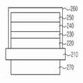
본 발명에 따른 X-선 검출용 유기소자(200)는 상기한 간접변환방식을 적용하기 위해 유기소자의 기판(210) 하부에 섬광체층(270)이 형성된다. 따라서 형성된 섬광체층(270)에 의해 입사되는 X-선이 가시광으로 변화하게 되고, 변화된 가시광이 활성층(240)에 도달하여 활성층(240)에서 생성되는 전하를 측정하게 된다.The X-ray detecting
섬광체층(270)에 사용될 수 있는 물질로는, 예를 들어, Nal:TI, Csl:TI, Y3Al5O12:Ce, CdWO4, LuAG:Ce,Gd2O2S:Tb등이 사용될 수 있으나, 바람직하게는 표 1에서와 같이 Maximum emission이 540nm를 갖고, PL output이 59000photons/MeV인 CsI:TI가 사용될 수 있다.CIWO4, LuAG: Ce, and Gd2O2S: Tb may be used as the material for the
섬광체층으로 CsI:TI를 사용하였을 때는 섬광체층의 두께를 1mm이하의 두께를 갖도록 하는 것이 바람직하다. 이는, 1mm 보다 두꺼운 섬광체층(270)은 섬광체층(270) 내부에서 생성된 가시광 Photon이 섬광체층(270) 내에서 재흡수가 일어나거나, 후면이 아닌 다른 방향으로 이동되는 이유에 기인하기 때문이다.When CsI: TI is used as the scintillator layer, it is preferable that the thickness of the scintillator layer has a thickness of 1 mm or less. This is because the
도 4 내지 도 8은 본 발명의 X-선 검출용 유기소자의 제작방법을 나타내는 도면이다.Figs. 4 to 8 are views showing a method of manufacturing an organic device for X-ray detection of the present invention.
도 4 내지 도 8을 참조하면, 본 발명의 X-선 검출용 유기소자(200)의 제작방법은 기판(210) 상부에 제1 전극층(220)을 형성하는 단계, 제1 전극층(220) 상부에 정공수송층(230)을 형성하는 단계, 정공수송층(230) 상부에 PCDTBT:PCBM의 혼합물로 형성된 활성층(240)을 형성하는 단계, 활성층(240) 상부에 제2 전극층(250)을 형성하는 단계 및 기판(210) 하부에 섬광체층(270)을 형성하는 단계를 포함한다.4 to 8, a method of manufacturing an
기판(210) 상부에 제1 전극층(220)을 형성하는 단계에서는 도 4에 도시한 바와 같이, 투명 유리나 유연성을 갖는 폴리머 기판(210) 상에 DC 스퍼터링 방식 또는 이와 달리 화학적 증착법(CVD), 원자층 증착(ALD), 졸겔 코팅(sol-gel coating), 전기도금 등에 의해 투명전극인 제1 전극층(220)이 형성될 수 있다. 기판(210)은 사용 직전에 세정공정을 거치며, 아세톤, 알콜, 물 혹은 이들의 혼합 용액에 담근 후 초음파 세정을 실시할 수도 있다. 이러한 투명전극의 두께는 바람직하게는 100~1,000nm일 수 있다. 또한, 사용되는 기판(210)은 바람직하게는 ITO 투명 전극이 코팅된 무알칼리 글라스(Non-Alkali Glass) 기판(210)일 수 있다.As shown in FIG. 4, in the step of forming the
제1 전극층(220) 상부에 정공수송층(230)을 형성하는 단계는 도 5에 도시한 바와 같이, 제1 전극층(220) 상부에 스핀 코팅법, 스프레이 코팅법, 스크린 인쇄법, 바(bar) 코팅법, 닥터블레이드 코팅법, 그라비아 프린팅법 등을 이용하여 정공수송층(Hole Transfer Layer, HTL)(230)을 형성할 수 있다. 이와 같이 형성된 정공수송층(230)의 두께는 바람직하게는 5~300nm일 수 있다. 정공수송층(230) 물질로는 TPD, PEDOT:PSS, G-PEDOT, PANI:PSS, PANI:CSA, PDBT, NPB, 아릴아민기(arylamine group)를 가지는 저분자와 고분자, 방향족아민기(aromatic amine group)를 가지는 저분자와 고분자 등일 수 있다.5, the step of forming the
정공수송층(230) 상부에 PCDTBT:PCBM로 형성된 활성층(240)을 형성하는 단계에서, 활성층(240)은 도너물질로 CuPc(copper phthalocyanine)과 같은 프탈로 시아닌계 안료, 인디고, 티오인디고계 안료, 멜로시아닌 화합물, 시아닌 화합물 등의 저분자 화합물과 폴리파라페닐렌비닐렌(poly-ρ-phenylenevinylene; PPV)등과 같은 페닐렌비닐렌계 고분자 유도체, 폴리티오펜(polythiophene), PCPDTBT, P3HT등과 같은 싸이오펜계 고분자 유도체 등을 포함하는 전도성 고분자가 이용될 수 있으나, 본 발명에 따른 바람직한 실시예에 따르면 도너물질로 PCPDTBT가 사용될 수 있다. 또한, 억셉터 물질로는 풀러렌(fullerene; C60), ICBA, ICBM, PCBM, PC70BM과 같은 풀러렌 유도체, 페릴렌(perylene), PTCBI와 같은 페릴렌 유도체, CdS, CdSe, CdTe, 또는 ZnSe와 같은 반도체 나노입자가 사용 될 수 있으나, 본 발명에 따른 바람직한 실시예에 따르면 억셉터 물질로 PCBM이 사용될 수 있다.In the step of forming the
즉, 본 발명에 따른 X-선 검출용 유기소자(200)의 활성층(240) 물질로써 도너물질인 PCPDTBT와 억셉터 물질인 PCBM를 혼합한 PCDTBT:PCBM 혼합물이 활성층(240)으로 사용될 수 있다. 여기서, PCDTBT:PCBM는 PCDTBT 1중량부에 대하여 PCBM 2 내지 4.5중량부로 이루어지는 것이 바람직하다. 더욱 상세하게는, PCDTBT:PCBM는 섬광체의 스팩트럼 특성과 비교하여 높은 정합도를 갖도록 PCDTBT와 PCBM의 중량비율로 1:4를 갖는 것이 바람직하다.That is, a PCDTBT: PCBM mixture in which the donor material PCPDTBT and the acceptor material PCBM are mixed can be used as the
상기한 PCDTBT:PCBM를 이용하여 활성용액이 형성되면, 활성용액을 정공수송층(230) 상부에 스핀 코팅, 스프레이 코팅, 스크린 인쇄 공정, 바 코팅, 닥터블레이드 코팅 및 그라비아 프린팅등을 이용하여 활성층(240)을 형성한다. 이렇게 형성된 PCDTBT:PCBM 혼합물을 포함하는 활성층 기반의 X-선 검출용 유기소자(200)는 종래의 P3HT:PCBM 혼합물을 포함하는 활성층 기반의 X-선 검출용 유기소자에 비해 가시광 영역의 흡광도가 우수하여 신호 취득 효율을 향상시킬 수 있다.When the active solution is formed using the PCDTBT: PCBM, the active layer is coated on the
활성층(240) 상부에 제2 전극층(250)을 형성하는 단계에서는 도 7에 도시한 바와 같이, 활성층(240) 상부에 활성층(240)에서 분리된 전자를 받아들이는 역할을 수행하는 제2 전극층(250)이 형성된다. 제2 전극층(250)은 알루미늄(Al), 아연(Zn), 타타늄(Ti), 인듐(In), 알칼리 금속, 나트륨-칼륨(Na:K)합금, 마그네슘-은(Mg:Ag)합금, 리튬-알루미늄(Li/Al)이층전극, 리튬플루오라이드-알루미늄(LiF/Al)이층전극과 같이 금속전극일 수 있으며, 활성층(240) 상부에 DC스퍼터링방식, 열증착 또는 이와 달리 화학적 증착법(CVD), 원자층증착(ALD), 전기도금 및 각종 프린팅기술과 같은 습식방식 등에 의해 형성될 수 있다. 도시하지는 않았지만 활성층(240)과 제2 전극층(250) 사이에는 생성된 전하의 취득효율을 높이기 위해 Alq3과 같은 전자수송층(미도시)이 활성층(240) 상부에 잉크젯방식, 오프셋 인쇄방식, 그라비아 인쇄방식 등으로 더 형성될 수 있다.7, the
제2 전극층(250)을 형성하는 단계 이후에는, 봉지(Encapsulation) 공정을 수행하는 단계를 더 포함할 수 있다. 봉지 공정은 유기소자를 공기 중의 수분과 산소로부터 보호하기 위해 제1 전극층(220), 정공수송층(230), 활성층(240) 및 제2 전극층(250)의 외부를 감싸도록 봉지층(260)이 형성될 수 있다.After the step of forming the
기판(210) 하부에 섬광체층(270)을 형성하는 단계는 도 9에 도시한 바와 같이, 상술한 봉지 공정에 의해 봉지층(260)을 형성한 이후에, 제작된 유기소자와 섬광체층(270) 사이의 광학적 손실을 최소화하기 위한 광학적 접착제(Optical Glue)등을 이용하여 섬광체층(270)이 유기소자의 기판(210)하부에 형성될 수 있다.The step of forming the
실험예Experimental Example
도 9는 본 발명에 따른 X-선 검출소자의 X-선 노출시 검출된 전하량을 나타내는 그래프이다.FIG. 9 is a graph showing the amount of charge detected by X-ray exposure of the X-ray detecting element according to the present invention.
도 9를 참조하면, 본 발명에 따른 실험예는 PCDTBT:PCBM를 기반으로 제작된 간접 방식 검출소자에서 X-선을 온, 오프하여 X-선을 조사하였을 때 생성된 전하량을 통해 소자의 성능을 평가하는 방식으로 진행하였다. 본 실험을 위해 의료용으로 주로 이용되는 관전압 80kVp, 63mAs의 인가 조건에서 본 발명의 유기소자(200)에 0.2~1.0V의 직류전압을 인가하여 X-선이 조사되었을 때 생성된 전하량을 음극에서 측정하였다.9, the experimental example according to the present invention shows that the performance of the device is improved by the amount of charge generated when the X-ray is irradiated and the X-ray is irradiated in the indirectly detecting device manufactured based on PCDTBT: PCBM . For this experiment, a DC voltage of 0.2 to 1.0 V was applied to the
측정결과 도 9에 도시한 바와 같이, 0.2V에서 1.0V로 인가전압이 증가할수록 음극에서 측정되는 전하량이 증가되는 것을 확인할 수 있다.Measurement results As shown in FIG. 9, it can be seen that as the applied voltage increases from 0.2 V to 1.0 V, the amount of charge measured at the cathode increases.
측정된 전하량을 기반으로 하여 본 발명에 따른 간접변환방식의 X-선 검출소자(200)에 대한 수집 전류 밀도(Collected CurrentDensity, CCD), 암 전류 밀도(Dark CurrentDensity, DCD) 및 X-선 검출감도(Sensitivity)를 각각 계산할 수 있다.(CCD), dark current density (DCD), and X-ray detection sensitivity for the
수집 전하 밀도를 계산하기 위한 수식을 수학식 1에 나타내었다.The formula for calculating the collected charge density is shown in Equation (1).

여기서, Exposed Time[s]*Detection Area[cm2]는 X-선 검출 영역을 의미하고, Charges duringX-rayON[nC]는 X-선이 조사될 때의 측정된 전하량을 의미한다.Here, Exposed Time [s] * Detection Area [cm 2 ] means the X-ray detection region and Charges during X-ray ON [nC] means the amount of charge measured when the X-ray is irradiated.
또한, 암 전류 밀도를 계산하기 위한 수식은 수학식 2에, 검출감도를 계산하기 위한 수식은 수학식 3에 각각 나타내었다.The formula for calculating the dark current density is shown in Equation (2), and the formula for calculating the detection sensitivity is shown in Equation (3).

여기서, Absorbed Dose[Gy]는 피복 선량, Detection Area[cm2]는 X선 검출 영역을 의미하고, CurrentduringX-ray ON은 X선이 조사될 때의 측정된 전하량을 의미한다.Here, the Absorbed Dose [Gy] denotes the coating dose, the Detection Area [cm 2 ] denotes the X-ray detection region, and the Currentduring X-ray ON denotes the measured amount of charge when the X-ray is irradiated.
상술한, 수집 전류 밀도, 암 전류 밀도 및 X-선 검출감도를 이용하여 본 발명에 따른 PCDTBT:PCBM 혼합 물질로 형성된 활성층을 포함하는 X-선 검출소자를 종래의 P3HT:PCBM 혼합 물질로 형성된 활성층을 포함하는 X-선 검출소자를 비교군으로 선정하여 비교 실험을 실시하였다.Using the above-described collecting current density, dark current density, and X-ray detection sensitivity, an X-ray detecting element including an active layer formed of a PCDTBT: PCBM mixed material according to the present invention is used as an active layer formed of a conventional P3HT: PCBM mixed material Were selected as a comparative group, and a comparative experiment was conducted.
도 10은 본 발명의 PCDTBT:PCBM 혼합 비율에 따른 간접변환방식의 X-선 검출소자의 특성을 나타낸 그래프이다.10 is a graph showing the characteristics of the indirect conversion type X-ray detection device according to the PCDTBT: PCBM mixture ratio of the present invention.
도 10을 참조하면, PCDTBT:PCBM 혼합 비율중 1:2 ~ 1:4.5에서 수집 전류 밀도, 암 전류 밀도 및 X-선 검출감도 특성이 높게 측정 되었으며, 특히, PCDTBT:PCBM의 혼합 비율중 1:4에서 수집 전류 밀도(CCD)=215.23nA/cm2, 암 전류 밀도(DCD)=7.59 nA/cm2, X-선 검출감도(Sensitivity)=1.55mA/Gy·2로 가장 우수한 특성이 나타남을 확인할 수 있다.10, the collecting current density, dark current density and X-ray detection sensitivity characteristics were measured to be high at 1: 2 to 1: 4.5 of the PCDTBT: PCBM blending ratio. Particularly, the blending ratio of PCDTBT: 4, the most excellent characteristics were observed at a collecting current density (CCD) of 215.23 nA / cm 2 , a dark current density (DCD) of 7.59 nA / cm 2 and an X-ray detection sensitivity of 1.55 mA / Gy 2 Can be confirmed.
즉, 혼합 비율이 1:2 이하가 되면, 도 10에서와 같이, 수집 전류 밀도가 낮아지기 때문에 검출감도가 가장 높은 혼합 비율 1:4 대비 8%이상 급격히 감소하며, 혼합 비율이 1:1에서는 검출감도가 38%나 감소되는 경향을 보인다. 또한, 혼합 비율이 1:4.5 이상이 되면, 암 전류 밀도의 증가와 수집 전류 밀도의 감소로 인한 검출감도의 손실을 보인다. 즉, PCDTBT:PCBM의 혼합 비율이 1:2 이하가 되거나, 1:4.5 이상이 되면, 검출감도가 감소되기 때문에 검출감도를 향상시키기 위해 X-선의 선량(dose) 증가가 요구되나, 이는 인체 X-선 검출기 적용시 환자에게 조사되는 피폭량이 증가되는 단점을 초래하게 된다.That is, when the mixing ratio is 1: 2 or less, as shown in FIG. 10, the collecting current density is lowered so that the detection sensitivity sharply decreases by 8% or more from the highest mixing ratio 1: 4, The sensitivity tends to decrease by 38%. Also, when the mixing ratio is 1: 4.5 or more, an increase in the dark current density and a loss in detection sensitivity due to a decrease in the collection current density are observed. That is, when the mixing ratio of PCDTBT: PCBM is 1: 2 or less and the ratio of PCDTBT: PCBM is 1: 4.5 or more, the detection sensitivity is decreased, so that dose increase of X-ray is required to improve detection sensitivity. - radiation detector, the amount of exposure to the patient is increased.
도 11은 본 발명의 PCDTBT:PCBM 혼합 비율에 따른 X-선 검출소자의 IPCE 특성을 나타낸 그래프이다.11 is a graph showing IPCE characteristics of the X-ray detecting device according to the PCDTBT: PCBM mixing ratio of the present invention.
도 11을 참조하면, 도 11은 회전속도(spin rate)를 1100rpm으로 고정하고 PCDTBT:PCBM의 혼합 비율을 변경하며, IPCE(Incident Photon-to-Current Efficiency) 특성을 측정한 그래프이다.Referring to FIG. 11, FIG. 11 is a graph illustrating the incidence photon-to-current efficiency (IPCE) characteristics of a PCDTBT: PCBM mixed ratio and a fixed spin rate of 1100 rpm.
도 11에 도시한 바와 같이, 섬광체의 발광 파장에 인접한 부분에서 PCDTBT:PCBM의 혼합 비율이 1:2 ~ 1:4.5 범위가 상대적으로 우수한 IPCE 특성이 나타남을 확인할 수 있다. 또한, PCDTBT:PCBM의 혼합 비율중 1:4에서 가장 우수한 IPCE 특성이 나타남을 확인 할 수 있다. 따라서, PCDTBT:PCBM의 혼합 비율이 1:4로 형성된 활성층이 섬광체와 결합 시 X-선 검출소자의 검출감도를 향상시킬 수 있음을 확인할 수 있다.As shown in FIG. 11, it can be seen that the IPCE characteristic of PCDTBT: PCBM in the portion adjacent to the emission wavelength of the scintillator is relatively excellent in the mixing ratio of 1: 2 to 1: 4.5. Also, it can be confirmed that the best IPCE characteristic is observed at 1: 4 of the mixing ratio of PCDTBT: PCBM. Therefore, it can be seen that the detection sensitivity of the X-ray detecting element can be improved when the active layer formed with the mixing ratio of PCDTBT: PCBM of 1: 4 is combined with the scintillator.
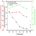
도 12는 본 발명의 PCDTBT:PCBM이 혼합된 활성층의 두께에 따른 특성 변화를 나타내는 그래프이다.12 is a graph showing a change in the characteristics of the active layer mixed with PCDTBT: PCBM according to the thickness of the present invention.
도 12를 참조하면, 도 12는 PCDTBT:PCBM의 혼합 비율중 특성이 가장 우수한 1:4 혼합 비율로 형성된 활성층의 두께를 변경하며 실험한 결과이며, 활성층의 두께 변경에 따른 수집 전류 밀도, 암 전류 밀도 및 X-선 검출감도를 측정한 결과를 나타낸다.12, FIG. 12 shows experimental results obtained by varying the thickness of the active layer formed at a mixing ratio of PCDTBT: PCBM of 1: 4, which is the best in the mixing ratio of PCDTBT: PCBM. Density and X-ray detection sensitivity.
도 12에 도시된 바와 같이, PCDTBT:PCBM이 혼합된 활성층의 두께가 65nm ~ 90nm 범위에서 수집 전류 밀도, 암 전류 밀도 및 X-선 검출감도가 향상되는 것을 확인할 수 있다. 만약, 활성층의 두께가 65nm 이하인 경우, 얇은 두께로 인한 급격한 암 전류 밀도의 증가(85nm 두께 대비 98%이상 증가)로 도 12에서와 같이, 검출감도가 감소하는 경향을 보이며, 활성층의 두께가 90nm 이상의 두께를 가지면 X-선 검출기의 경우, 활성층에서 생성된 전하가 전극으로 이동하며 발생하는 손실로 인한 수집 전류 밀도의 감소로 검출감도가 감소하게 된다. 따라서, 활성층의 두께가 90nm 이상이 되면 검출감도를 증가시키기 위해 X-선의 선량(dose) 증가가 요구되기 때문에 환자에게 조사되는 피폭량이 증가되는 단점을 초래하게 된다.As shown in FIG. 12, it can be seen that the collection current density, dark current density and X-ray detection sensitivity are improved in the range of 65 nm to 90 nm in thickness of the active layer in which PCDTBT: PCBM is mixed. If the thickness of the active layer is 65 nm or less, the detection sensitivity tends to decrease with an increase in the abrupt dark current density (98% or more as compared with the 85 nm thickness) due to the thin thickness, , The detection sensitivity of the X-ray detector is reduced due to the reduction of the collection current density due to the loss caused by the charge generated in the active layer moving to the electrode. Therefore, when the thickness of the active layer is 90 nm or more, an increase in dose of X-ray is required to increase the detection sensitivity, which leads to an increase in the amount of exposure to the patient.
또한, PCDTBT:PCBM이 혼합된 활성층의 두께 중에서는 두께가 85nm 일 때, 수집 전류 밀도=235.58nA/cm2, 암 전류 밀도=9.68nA/cm2, X-선 검출감도=1.69mA/Gy·2로 가장 우수한 특성이 나타남을 확인 할 수 있다.In addition, when the thickness of the active layer mixed with PCDTBT: PCBM is 85 nm, the collecting current density is 235.58 nA / cm 2 , the dark current density is 9.68 nA / cm 2 and the X-ray detection sensitivity is 1.69 mA / Gy · 2 shows the best properties.
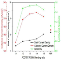
도 13는 X-선 검출용 유기소자의 두 가지 활성층 물질(P3HT:PCBM, PCDTBT:PCBM)에 대한 민감도와 암 전류 밀도를 비교하기 위한 그래프이다.13 is a graph for comparing the sensitivity and the dark current density for the two active layer materials (P3HT: PCBM, PCDTBT: PCBM) of the organic device for X-ray detection.
또한, 도 13에 도시된 그래프에 따른 데이터를 표 2에 나타내었다.Data according to the graph shown in FIG. 13 are also shown in Table 2.
[nC/mR*cm2]Sensitivity
[nC / mR * cm 2]
[nA/cm2]Dark CurrentDensity
[nA / cm 2 ]
도 13 및 표 2를 참조하면, 본 발명에 따른 PCDTBT:PCBM 기반 X-선 검출용 유기소자(200)의 경우 종래의 P3HT:PCBM 기반 X-선 검출용 유기소자에 비해 동일 전압 조건에서 X-선 검출감도가 33.7% 향상된 것을 확인할 수 있으며, 암 전류(X-선이 없는 상황에서 동일 전압을 인가 시 유기검출소자에서 측정되는 전류) 밀도의 경우 18.7% 감소된 효과를 확인 할 수 있다.Referring to FIG. 13 and Table 2, the PCDTBT: PCBM-based X-ray detecting
상술한 바와 같이, 종래의 P3HT:PCBM의 혼합물질을 기반으로 한 활성층(240)을 포함하는 X-선 검출용 유기소자의 경우 가시광 영역의 흡광도가 저조하여 조사된 X-선이 섬광체에 의해 빛으로 변환되어 검출소자에 입사될 경우 그 흡수율이 낮은 단점을 가지고 있으나, 본 발명에 따른 PCDTBT:PCBM 혼합물질을 기반으로 한 활성층(240)을 포함하는 X-선 검출용 유기소자(200)의 경우 종래의 P3HT:PCBM 대비 가시광 영역의 흡광도가 우수하여 신호 취득 효율을 향상시킬 수 있는 장점이 있다.As described above, in the case of an organic device for X-ray detection including an
한편, 본 명세서와 도면에 개시된 본 발명의 실시 예들은 이해를 돕기 위해 특정 예를 제시한 것에 지나지 않으며, 본 발명의 범위를 한정하고자 하는 것은 아니다. 여기에 개시된 실시 예들 이외에도 본 발명의 기술적 사상에 바탕을 둔 다른 변형 예들이 실시 가능하다는 것은, 본 발명이 속하는 기술 분야에서 통상의 지식을 가진 자에게 자명한 것이다.It should be noted that the embodiments of the present invention disclosed in the present specification and drawings are only illustrative of specific examples for the purpose of understanding and are not intended to limit the scope of the present invention. It will be apparent to those skilled in the art that other modifications based on the technical idea of the present invention are possible in addition to the embodiments disclosed herein.
210 : 기판
220 : 제1 전극층
230 : 정공수송층
240 : 활성층
250 : 제2 전극층
260 : 봉지층
270 : 섬광체층210: substrate 220: first electrode layer
230: hole transport layer 240: active layer
250: second electrode layer 260: sealing layer
270:
Claims (15)
상기 기판 상부에 형성되는 제1 전극층;
상기 제1 전극층 상부에 형성되고, 정공의 수송을 향상시키는 정공수송층;
상기 정공수송층 상부에 형성되고, 상기 기판 하부에서 발생한 가시광선을 흡수하여 전자-정공 쌍을 생성하는 활성층;
상기 활성층 상부에 형성되는 제2 전극층; 및
상기 기판 하부에 형성되며, X-선을 가시광선으로 변환하는 섬광체층(scintillator);을 포함하고,
상기 활성층은 PCDTBT:PCBM의 혼합물로 형성되는 것을 특징으로 하는 X-선 검출용 유기소자.Board;
A first electrode layer formed on the substrate;
A hole transport layer formed on the first electrode layer and improving transport of holes;
An active layer formed on the hole transport layer and absorbing visible light generated from the bottom of the substrate to generate electron-hole pairs;
A second electrode layer formed on the active layer; And
And a scintillator formed below the substrate, the scintillator converting X-rays into visible light,
Wherein the active layer is formed of a mixture of PCDTBT: PCBM.
상기 PCDTBT:PCBM는 상기 PCDTBT 1중량부에 대하여 PCBM 2 내지 4.5중량부로 이루어지는 것인 X-선 검출용 유기소자.The method according to claim 1,
Wherein the PCDTBT: PCBM is composed of 2 to 4.5 parts by weight of PCBM per 1 part by weight of the PCDTBT.
상기 PCDTBT:PCBM는 상기 섬광체층의 스팩트럼 특성과 비교하여 높은 정합도를 갖도록 PCDTBT 1중량부에 대하여 PCBM 4중량부를 갖는 것인 X-선 검출용 유기소자.The method according to claim 1,
Wherein the PCDTBT: PCBM has 4 parts by weight of PCBM relative to 1 part by weight of PCDTBT so as to have a high degree of matching in comparison with the spectral characteristics of the scintillator layer.
상기 PCDTBT:PCBM이 혼합된 상기 활성층은 65nm 내지 90nm의 두께를 갖는 것인 X-선 검출용 유기소자.The method according to claim 1,
Wherein the active layer mixed with PCDTBT: PCBM has a thickness of 65 nm to 90 nm.
상기 PCDTBT:PCBM이 혼합된 상기 활성층은 85nm의 두께를 갖는 것인 X-선 검출용 유기소자.The method according to claim 1,
Wherein the active layer in which the PCDTBT: PCBM is mixed has a thickness of 85 nm.
상기 섬광체층은 Nal:TI, Csl:TI, Y3Al5O12:Ce, CdWO4, LuAG:Ce및 Gd2O2S:Tb로 이루어진 군에서 어느 하나로 형성되는 것인 X-선 검출용 유기소자.The method according to claim 1,
Wherein the scintillator layer is formed of any one selected from the group consisting of Nal: TI, CsI: TI, Y3Al5O12: Ce, CdWO4, LuAG: Ce and Gd2O2S: Tb.
상기 Csl:TI 물질로 형성된 섬광체층의 발광도와 상기 PCDTBT:PCBM이 혼합된 활성층의 흡광도가 500 내지 650nm 파장 영역에서 겹치는 것인 X-선 검출용 유기소자.The method according to claim 6,
Wherein an emission of the scintillator layer formed of the Csl: TI material and an absorbance of the active layer mixed with the PCDTBT: PCBM overlap in a wavelength range of 500 to 650 nm.
상기 섬광체층은 1mm이하의 두께를 갖는 것인 X-선 검출용 유기소자.The method according to claim 1,
Wherein the scintillator layer has a thickness of 1 mm or less.
상기 제1 전극층 상부에 정공수송층을 형성하는 단계;
상기 정공수송층 상부에 PCDTBT:PCBM의 혼합물로 형성된 활성층을 형성하는 단계;
상기 활성층 상부에 제2 전극층을 형성하는 단계; 및
상기 기판 하부에 섬광체층(scintillator)을 형성하는 단계를 포함하는 X-선 검출용 유기소자의 제조방법.Forming a first electrode layer on the substrate;
Forming a hole transport layer on the first electrode layer;
Forming an active layer formed of a mixture of PCDTBT: PCBM on the hole transport layer;
Forming a second electrode layer on the active layer; And
And forming a scintillator on the lower surface of the substrate.
상기 기판은 ITO 투명 전극이 코팅된 무알칼리 글라스(Non-Alkali Glass) 기판인 것인 X-선 검출용 유기소자의 제조방법.10. The method of claim 9, wherein in forming the first electrode layer on the substrate,
Wherein the substrate is a non-alkali glass substrate coated with an ITO transparent electrode.
상기 PCDTBT:PCBM는 상기 PCDTBT 1중량부에 대하여 PCBM 2 내지 4.5중량부로 이루어지는 것인 X-선 검출용 유기소자의 제조방법.10. The method according to claim 9, wherein, in the step of forming the active layer,
Wherein the PCDTBT: PCBM comprises 2 to 4.5 parts by weight of PCBM per 1 part by weight of the PCDTBT.
상기 PCDTBT:PCBM이 혼합된 상기 활성층은 65nm 내지 90nm의 두께를 갖는 것인 X-선 검출용 유기소자의 제조방법.10. The method according to claim 9, wherein, in the step of forming the active layer,
Wherein the active layer in which the PCDTBT: PCBM is mixed has a thickness of 65 nm to 90 nm.
상기 섬광체층은 Nal:TI, Csl:TI, Y3Al5O12:Ce, CdWO4, LuAG:Ce및 Gd2O2S:Tb로 이루어진 군에서 어느 하나로 형성되는 것인 X-선 검출용 유기소자의 제조방법.The method according to claim 9, wherein in the step of forming the scintillator layer,
Wherein the scintillator layer is formed of any one of the group consisting of Nal: TI, CsI: TI, Y3Al5O12: Ce, CdWO4, LuAG: Ce and Gd2O2S: Tb.
상기 Csl:TI 물질로 형성된 섬광체층의 발광도와 상기 PCDTBT:PCBM이 혼합된 활성층의 흡광도가 500 내지 650nm 파장 영역에서 겹치는 것인 X-선 검출용 유기소자의 제조방법.14. The method of claim 13,
Wherein the luminescence of the scintillator layer formed of the Csl: TI material and the absorbance of the active layer mixed with the PCDTBT: PCBM overlap in the wavelength range of 500 to 650 nm.
상기 제2 전극층을 형성하는 단계 이후에 봉지(Encapsulation)공정을 수행하는 단계를 더 포함하는 것인 X-선 검출용 유기소자의 제조방법.10. The method of claim 9,
And performing an encapsulation process after the step of forming the second electrode layer.
Applications Claiming Priority (2)
| Application Number | Priority Date | Filing Date | Title |
|---|---|---|---|
| KR1020170024610 | 2017-02-24 | ||
| KR20170024610 | 2017-02-24 |
Publications (2)
| Publication Number | Publication Date |
|---|---|
| KR20180098170A true KR20180098170A (en) | 2018-09-03 |
| KR102067546B1 KR102067546B1 (en) | 2020-01-17 |
Family
ID=63600882
Family Applications (1)
| Application Number | Title | Priority Date | Filing Date |
|---|---|---|---|
| KR1020180022136A KR102067546B1 (en) | 2017-02-24 | 2018-02-23 | Organic device for X-ray detect and method of manufacturing the same |
Country Status (1)
| Country | Link |
|---|---|
| KR (1) | KR102067546B1 (en) |
Cited By (1)
| Publication number | Priority date | Publication date | Assignee | Title |
|---|---|---|---|---|
| KR20210055835A (en) * | 2019-11-07 | 2021-05-18 | 단국대학교 산학협력단 | X-ray Detect and Method of Manufacturing the Same |
Citations (6)
| Publication number | Priority date | Publication date | Assignee | Title |
|---|---|---|---|---|
| KR20100091024A (en) * | 2009-02-09 | 2010-08-18 | 광주과학기술원 | Light emitting organic photovoltaic cells and mathod of manufacturing the same |
| KR101412896B1 (en) | 2012-05-09 | 2014-06-26 | 주식회사 엘지화학 | Organic electrochemical device and fabrication method thereof |
| US20150034910A1 (en) * | 2013-07-31 | 2015-02-05 | General Electric Company | Organic x-ray detector |
| JP5741702B2 (en) * | 2011-10-20 | 2015-07-01 | 富士通株式会社 | Photoelectric conversion element and manufacturing method thereof |
| KR20150094914A (en) * | 2014-02-12 | 2015-08-20 | 단국대학교 산학협력단 | Organic device for detecting x-ray image based on coplanar electrode structure and thereof manufacture method |
| JP2015206660A (en) * | 2014-04-18 | 2015-11-19 | 株式会社ネモト・ルミマテリアル | X ray phosphor plate |
-
2018
- 2018-02-23 KR KR1020180022136A patent/KR102067546B1/en active IP Right Grant
Patent Citations (6)
| Publication number | Priority date | Publication date | Assignee | Title |
|---|---|---|---|---|
| KR20100091024A (en) * | 2009-02-09 | 2010-08-18 | 광주과학기술원 | Light emitting organic photovoltaic cells and mathod of manufacturing the same |
| JP5741702B2 (en) * | 2011-10-20 | 2015-07-01 | 富士通株式会社 | Photoelectric conversion element and manufacturing method thereof |
| KR101412896B1 (en) | 2012-05-09 | 2014-06-26 | 주식회사 엘지화학 | Organic electrochemical device and fabrication method thereof |
| US20150034910A1 (en) * | 2013-07-31 | 2015-02-05 | General Electric Company | Organic x-ray detector |
| KR20150094914A (en) * | 2014-02-12 | 2015-08-20 | 단국대학교 산학협력단 | Organic device for detecting x-ray image based on coplanar electrode structure and thereof manufacture method |
| JP2015206660A (en) * | 2014-04-18 | 2015-11-19 | 株式会社ネモト・ルミマテリアル | X ray phosphor plate |
Cited By (1)
| Publication number | Priority date | Publication date | Assignee | Title |
|---|---|---|---|---|
| KR20210055835A (en) * | 2019-11-07 | 2021-05-18 | 단국대학교 산학협력단 | X-ray Detect and Method of Manufacturing the Same |
Also Published As
| Publication number | Publication date |
|---|---|
| KR102067546B1 (en) | 2020-01-17 |
Similar Documents
| Publication | Publication Date | Title |
|---|---|---|
| CN106796301B (en) | Organic photodiode, organic x-ray detector and x-ray system | |
| JP5141685B2 (en) | Method for manufacturing photoelectric conversion element | |
| US20140191218A1 (en) | X-ray-sensitive devices and systems using organic pn junction photodiodes | |
| KR20190102182A (en) | Direct conversion radiation detector | |
| WO2011052565A1 (en) | Organic photoelectric conversion element | |
| WO2011052571A1 (en) | Organic photovoltaic conversion element | |
| EP3195361A1 (en) | X-ray detector and x-ray systems using organic photodiodes | |
| US11877459B2 (en) | Light detecting element | |
| US9362341B2 (en) | X ray detection apparatus | |
| KR20170029363A (en) | Organic Device for Detecting Radiation and Thereof Manufacture Method | |
| US20220246873A1 (en) | Self-powered perovskite x-ray detector | |
| US20150034910A1 (en) | Organic x-ray detector | |
| Lee et al. | Characteristics of a flexible radiation detector fabricated with non-fullerene acceptor for an Indirect-type X-ray imaging | |
| Seon et al. | Characteristic of an Organic Photodetector fabricated with P3HT: ICBA blending materials for Indirect X-ray Detection | |
| Iacchetti et al. | Multi-layer organic squaraine-based photodiode for indirect X-ray detection | |
| KR102067546B1 (en) | Organic device for X-ray detect and method of manufacturing the same | |
| KR102380472B1 (en) | X-ray Detect and Method of Manufacturing the Same | |
| KR101972636B1 (en) | Organic device for X-ray detect and method of manufacturing the same | |
| Lee et al. | Comparative studies between photovoltaic and radiation parameters in indirect-type organic X-ray detector with a P3HT: PCBM active layer | |
| An et al. | Spectral response tuning of organic photodetectors using strong microcavity effects for medical X-ray detector application | |
| US9812510B1 (en) | Packaging organic photodetectors | |
| KR20200011654A (en) | X-ray detection organic device and manufacturing method thereof | |
| US20210305523A1 (en) | Light detecting element | |
| Seon et al. | A study on the characteristics of indirect-type organic detector using p-type polycarbazole copolymer for X-ray imaging | |
| US20170301735A1 (en) | Charge integrating devices and related systems |
Legal Events
| Date | Code | Title | Description |
|---|---|---|---|
| A201 | Request for examination | ||
| E902 | Notification of reason for refusal | ||
| AMND | Amendment | ||
| E601 | Decision to refuse application | ||
| X091 | Application refused [patent] | ||
| AMND | Amendment | ||
| X701 | Decision to grant (after re-examination) | ||
| GRNT | Written decision to grant |