KR20180098138A - Method for forming planarized etch mask structures over existing topography - Google Patents
Method for forming planarized etch mask structures over existing topography Download PDFInfo
- Publication number
- KR20180098138A KR20180098138A KR1020180017407A KR20180017407A KR20180098138A KR 20180098138 A KR20180098138 A KR 20180098138A KR 1020180017407 A KR1020180017407 A KR 1020180017407A KR 20180017407 A KR20180017407 A KR 20180017407A KR 20180098138 A KR20180098138 A KR 20180098138A
- Authority
- KR
- South Korea
- Prior art keywords
- layer
- feature
- substrate
- multilayer stack
- stack
- Prior art date
Links
Images


Classifications
-
- H—ELECTRICITY
- H01—ELECTRIC ELEMENTS
- H01L—SEMICONDUCTOR DEVICES NOT COVERED BY CLASS H10
- H01L21/00—Processes or apparatus adapted for the manufacture or treatment of semiconductor or solid state devices or of parts thereof
- H01L21/02—Manufacture or treatment of semiconductor devices or of parts thereof
- H01L21/027—Making masks on semiconductor bodies for further photolithographic processing not provided for in group H01L21/18 or H01L21/34
- H01L21/033—Making masks on semiconductor bodies for further photolithographic processing not provided for in group H01L21/18 or H01L21/34 comprising inorganic layers
- H01L21/0332—Making masks on semiconductor bodies for further photolithographic processing not provided for in group H01L21/18 or H01L21/34 comprising inorganic layers characterised by their composition, e.g. multilayer masks, materials
-
- H—ELECTRICITY
- H01—ELECTRIC ELEMENTS
- H01L—SEMICONDUCTOR DEVICES NOT COVERED BY CLASS H10
- H01L21/00—Processes or apparatus adapted for the manufacture or treatment of semiconductor or solid state devices or of parts thereof
- H01L21/02—Manufacture or treatment of semiconductor devices or of parts thereof
- H01L21/027—Making masks on semiconductor bodies for further photolithographic processing not provided for in group H01L21/18 or H01L21/34
- H01L21/033—Making masks on semiconductor bodies for further photolithographic processing not provided for in group H01L21/18 or H01L21/34 comprising inorganic layers
- H01L21/0334—Making masks on semiconductor bodies for further photolithographic processing not provided for in group H01L21/18 or H01L21/34 comprising inorganic layers characterised by their size, orientation, disposition, behaviour, shape, in horizontal or vertical plane
- H01L21/0337—Making masks on semiconductor bodies for further photolithographic processing not provided for in group H01L21/18 or H01L21/34 comprising inorganic layers characterised by their size, orientation, disposition, behaviour, shape, in horizontal or vertical plane characterised by the process involved to create the mask, e.g. lift-off masks, sidewalls, or to modify the mask, e.g. pre-treatment, post-treatment
-
- H—ELECTRICITY
- H01—ELECTRIC ELEMENTS
- H01L—SEMICONDUCTOR DEVICES NOT COVERED BY CLASS H10
- H01L21/00—Processes or apparatus adapted for the manufacture or treatment of semiconductor or solid state devices or of parts thereof
- H01L21/02—Manufacture or treatment of semiconductor devices or of parts thereof
- H01L21/04—Manufacture or treatment of semiconductor devices or of parts thereof the devices having at least one potential-jump barrier or surface barrier, e.g. PN junction, depletion layer or carrier concentration layer
- H01L21/18—Manufacture or treatment of semiconductor devices or of parts thereof the devices having at least one potential-jump barrier or surface barrier, e.g. PN junction, depletion layer or carrier concentration layer the devices having semiconductor bodies comprising elements of Group IV of the Periodic System or AIIIBV compounds with or without impurities, e.g. doping materials
- H01L21/30—Treatment of semiconductor bodies using processes or apparatus not provided for in groups H01L21/20 - H01L21/26
- H01L21/302—Treatment of semiconductor bodies using processes or apparatus not provided for in groups H01L21/20 - H01L21/26 to change their surface-physical characteristics or shape, e.g. etching, polishing, cutting
- H01L21/306—Chemical or electrical treatment, e.g. electrolytic etching
- H01L21/308—Chemical or electrical treatment, e.g. electrolytic etching using masks
- H01L21/3081—Chemical or electrical treatment, e.g. electrolytic etching using masks characterised by their composition, e.g. multilayer masks, materials
-
- G—PHYSICS
- G03—PHOTOGRAPHY; CINEMATOGRAPHY; ANALOGOUS TECHNIQUES USING WAVES OTHER THAN OPTICAL WAVES; ELECTROGRAPHY; HOLOGRAPHY
- G03F—PHOTOMECHANICAL PRODUCTION OF TEXTURED OR PATTERNED SURFACES, e.g. FOR PRINTING, FOR PROCESSING OF SEMICONDUCTOR DEVICES; MATERIALS THEREFOR; ORIGINALS THEREFOR; APPARATUS SPECIALLY ADAPTED THEREFOR
- G03F7/00—Photomechanical, e.g. photolithographic, production of textured or patterned surfaces, e.g. printing surfaces; Materials therefor, e.g. comprising photoresists; Apparatus specially adapted therefor
- G03F7/0002—Lithographic processes using patterning methods other than those involving the exposure to radiation, e.g. by stamping
-
- H—ELECTRICITY
- H01—ELECTRIC ELEMENTS
- H01L—SEMICONDUCTOR DEVICES NOT COVERED BY CLASS H10
- H01L21/00—Processes or apparatus adapted for the manufacture or treatment of semiconductor or solid state devices or of parts thereof
- H01L21/02—Manufacture or treatment of semiconductor devices or of parts thereof
- H01L21/02104—Forming layers
- H01L21/02107—Forming insulating materials on a substrate
- H01L21/02109—Forming insulating materials on a substrate characterised by the type of layer, e.g. type of material, porous/non-porous, pre-cursors, mixtures or laminates
- H01L21/02112—Forming insulating materials on a substrate characterised by the type of layer, e.g. type of material, porous/non-porous, pre-cursors, mixtures or laminates characterised by the material of the layer
- H01L21/02115—Forming insulating materials on a substrate characterised by the type of layer, e.g. type of material, porous/non-porous, pre-cursors, mixtures or laminates characterised by the material of the layer the material being carbon, e.g. alpha-C, diamond or hydrogen doped carbon
-
- H—ELECTRICITY
- H01—ELECTRIC ELEMENTS
- H01L—SEMICONDUCTOR DEVICES NOT COVERED BY CLASS H10
- H01L21/00—Processes or apparatus adapted for the manufacture or treatment of semiconductor or solid state devices or of parts thereof
- H01L21/02—Manufacture or treatment of semiconductor devices or of parts thereof
- H01L21/02104—Forming layers
- H01L21/02107—Forming insulating materials on a substrate
- H01L21/02225—Forming insulating materials on a substrate characterised by the process for the formation of the insulating layer
- H01L21/0226—Forming insulating materials on a substrate characterised by the process for the formation of the insulating layer formation by a deposition process
- H01L21/02282—Forming insulating materials on a substrate characterised by the process for the formation of the insulating layer formation by a deposition process liquid deposition, e.g. spin-coating, sol-gel techniques, spray coating
-
- H—ELECTRICITY
- H01—ELECTRIC ELEMENTS
- H01L—SEMICONDUCTOR DEVICES NOT COVERED BY CLASS H10
- H01L21/00—Processes or apparatus adapted for the manufacture or treatment of semiconductor or solid state devices or of parts thereof
- H01L21/02—Manufacture or treatment of semiconductor devices or of parts thereof
- H01L21/027—Making masks on semiconductor bodies for further photolithographic processing not provided for in group H01L21/18 or H01L21/34
- H01L21/0271—Making masks on semiconductor bodies for further photolithographic processing not provided for in group H01L21/18 or H01L21/34 comprising organic layers
- H01L21/0273—Making masks on semiconductor bodies for further photolithographic processing not provided for in group H01L21/18 or H01L21/34 comprising organic layers characterised by the treatment of photoresist layers
- H01L21/0274—Photolithographic processes
-
- H—ELECTRICITY
- H01—ELECTRIC ELEMENTS
- H01L—SEMICONDUCTOR DEVICES NOT COVERED BY CLASS H10
- H01L21/00—Processes or apparatus adapted for the manufacture or treatment of semiconductor or solid state devices or of parts thereof
- H01L21/02—Manufacture or treatment of semiconductor devices or of parts thereof
- H01L21/04—Manufacture or treatment of semiconductor devices or of parts thereof the devices having at least one potential-jump barrier or surface barrier, e.g. PN junction, depletion layer or carrier concentration layer
- H01L21/18—Manufacture or treatment of semiconductor devices or of parts thereof the devices having at least one potential-jump barrier or surface barrier, e.g. PN junction, depletion layer or carrier concentration layer the devices having semiconductor bodies comprising elements of Group IV of the Periodic System or AIIIBV compounds with or without impurities, e.g. doping materials
- H01L21/30—Treatment of semiconductor bodies using processes or apparatus not provided for in groups H01L21/20 - H01L21/26
- H01L21/302—Treatment of semiconductor bodies using processes or apparatus not provided for in groups H01L21/20 - H01L21/26 to change their surface-physical characteristics or shape, e.g. etching, polishing, cutting
- H01L21/306—Chemical or electrical treatment, e.g. electrolytic etching
- H01L21/308—Chemical or electrical treatment, e.g. electrolytic etching using masks
- H01L21/3083—Chemical or electrical treatment, e.g. electrolytic etching using masks characterised by their size, orientation, disposition, behaviour, shape, in horizontal or vertical plane
- H01L21/3086—Chemical or electrical treatment, e.g. electrolytic etching using masks characterised by their size, orientation, disposition, behaviour, shape, in horizontal or vertical plane characterised by the process involved to create the mask, e.g. lift-off masks, sidewalls, or to modify the mask, e.g. pre-treatment, post-treatment
-
- H—ELECTRICITY
- H01—ELECTRIC ELEMENTS
- H01L—SEMICONDUCTOR DEVICES NOT COVERED BY CLASS H10
- H01L21/00—Processes or apparatus adapted for the manufacture or treatment of semiconductor or solid state devices or of parts thereof
- H01L21/02—Manufacture or treatment of semiconductor devices or of parts thereof
- H01L21/04—Manufacture or treatment of semiconductor devices or of parts thereof the devices having at least one potential-jump barrier or surface barrier, e.g. PN junction, depletion layer or carrier concentration layer
- H01L21/18—Manufacture or treatment of semiconductor devices or of parts thereof the devices having at least one potential-jump barrier or surface barrier, e.g. PN junction, depletion layer or carrier concentration layer the devices having semiconductor bodies comprising elements of Group IV of the Periodic System or AIIIBV compounds with or without impurities, e.g. doping materials
- H01L21/30—Treatment of semiconductor bodies using processes or apparatus not provided for in groups H01L21/20 - H01L21/26
- H01L21/302—Treatment of semiconductor bodies using processes or apparatus not provided for in groups H01L21/20 - H01L21/26 to change their surface-physical characteristics or shape, e.g. etching, polishing, cutting
- H01L21/306—Chemical or electrical treatment, e.g. electrolytic etching
- H01L21/308—Chemical or electrical treatment, e.g. electrolytic etching using masks
- H01L21/3083—Chemical or electrical treatment, e.g. electrolytic etching using masks characterised by their size, orientation, disposition, behaviour, shape, in horizontal or vertical plane
- H01L21/3088—Process specially adapted to improve the resolution of the mask
-
- H—ELECTRICITY
- H01—ELECTRIC ELEMENTS
- H01L—SEMICONDUCTOR DEVICES NOT COVERED BY CLASS H10
- H01L21/00—Processes or apparatus adapted for the manufacture or treatment of semiconductor or solid state devices or of parts thereof
- H01L21/02—Manufacture or treatment of semiconductor devices or of parts thereof
- H01L21/04—Manufacture or treatment of semiconductor devices or of parts thereof the devices having at least one potential-jump barrier or surface barrier, e.g. PN junction, depletion layer or carrier concentration layer
- H01L21/18—Manufacture or treatment of semiconductor devices or of parts thereof the devices having at least one potential-jump barrier or surface barrier, e.g. PN junction, depletion layer or carrier concentration layer the devices having semiconductor bodies comprising elements of Group IV of the Periodic System or AIIIBV compounds with or without impurities, e.g. doping materials
- H01L21/30—Treatment of semiconductor bodies using processes or apparatus not provided for in groups H01L21/20 - H01L21/26
- H01L21/31—Treatment of semiconductor bodies using processes or apparatus not provided for in groups H01L21/20 - H01L21/26 to form insulating layers thereon, e.g. for masking or by using photolithographic techniques; After treatment of these layers; Selection of materials for these layers
- H01L21/3105—After-treatment
- H01L21/31051—Planarisation of the insulating layers
-
- H—ELECTRICITY
- H01—ELECTRIC ELEMENTS
- H01L—SEMICONDUCTOR DEVICES NOT COVERED BY CLASS H10
- H01L21/00—Processes or apparatus adapted for the manufacture or treatment of semiconductor or solid state devices or of parts thereof
- H01L21/02—Manufacture or treatment of semiconductor devices or of parts thereof
- H01L21/04—Manufacture or treatment of semiconductor devices or of parts thereof the devices having at least one potential-jump barrier or surface barrier, e.g. PN junction, depletion layer or carrier concentration layer
- H01L21/18—Manufacture or treatment of semiconductor devices or of parts thereof the devices having at least one potential-jump barrier or surface barrier, e.g. PN junction, depletion layer or carrier concentration layer the devices having semiconductor bodies comprising elements of Group IV of the Periodic System or AIIIBV compounds with or without impurities, e.g. doping materials
- H01L21/30—Treatment of semiconductor bodies using processes or apparatus not provided for in groups H01L21/20 - H01L21/26
- H01L21/31—Treatment of semiconductor bodies using processes or apparatus not provided for in groups H01L21/20 - H01L21/26 to form insulating layers thereon, e.g. for masking or by using photolithographic techniques; After treatment of these layers; Selection of materials for these layers
- H01L21/3105—After-treatment
- H01L21/311—Etching the insulating layers by chemical or physical means
- H01L21/31105—Etching inorganic layers
- H01L21/31111—Etching inorganic layers by chemical means
-
- H—ELECTRICITY
- H01—ELECTRIC ELEMENTS
- H01L—SEMICONDUCTOR DEVICES NOT COVERED BY CLASS H10
- H01L21/00—Processes or apparatus adapted for the manufacture or treatment of semiconductor or solid state devices or of parts thereof
- H01L21/70—Manufacture or treatment of devices consisting of a plurality of solid state components formed in or on a common substrate or of parts thereof; Manufacture of integrated circuit devices or of parts thereof
- H01L21/71—Manufacture of specific parts of devices defined in group H01L21/70
- H01L21/768—Applying interconnections to be used for carrying current between separate components within a device comprising conductors and dielectrics
- H01L21/76801—Applying interconnections to be used for carrying current between separate components within a device comprising conductors and dielectrics characterised by the formation and the after-treatment of the dielectrics, e.g. smoothing
- H01L21/76802—Applying interconnections to be used for carrying current between separate components within a device comprising conductors and dielectrics characterised by the formation and the after-treatment of the dielectrics, e.g. smoothing by forming openings in dielectrics
- H01L21/76816—Aspects relating to the layout of the pattern or to the size of vias or trenches
Landscapes
- Engineering & Computer Science (AREA)
- Physics & Mathematics (AREA)
- General Physics & Mathematics (AREA)
- Manufacturing & Machinery (AREA)
- Condensed Matter Physics & Semiconductors (AREA)
- Computer Hardware Design (AREA)
- Microelectronics & Electronic Packaging (AREA)
- Power Engineering (AREA)
- Chemical & Material Sciences (AREA)
- Inorganic Chemistry (AREA)
- General Chemical & Material Sciences (AREA)
- Chemical Kinetics & Catalysis (AREA)
- Drying Of Semiconductors (AREA)
- Exposure Of Semiconductors, Excluding Electron Or Ion Beam Exposure (AREA)
- Laminated Bodies (AREA)
- Shaping Of Tube Ends By Bending Or Straightening (AREA)
Abstract
Description
나노 제조는 대략 100 나노미터 또는 그 이하의 피쳐(feature)를 갖는 매우 작은 구조의 제조를 포함한다. 나노 제조가 상당한 영향을 미친 한 가지 응용은 집적 회로의 처리에 있다. 반도체 처리 산업은 기판 상에 형성된 단위 면적당 회로를 증가시키면서 더 큰 생산 수율을 위해 계속 노력하고 있으며; 따라서 나노 제조가 점차 중요해지고 있다. 나노 제조는 더 큰 프로세스 제어를 제공하면서 형성되는 구조물의 최소 피쳐 치수의 지속적인 감소를 허용한다.Nano fabrication involves the fabrication of very small structures with features of about 100 nanometers or less. One application where nanofabrication has had a significant impact is in the processing of integrated circuits. The semiconductor processing industry continues to strive for greater production yield while increasing circuitry per unit area formed on the substrate; Therefore, nano fabrication is becoming increasingly important. Nano fabrication allows for continued reduction of the minimum feature dimensions of the structure being formed while providing greater process control.
이러한 구조를 형성하는 피쳐를 패터닝하기 위해 현재 사용되는 예시적인 나노 제조 기술은 광학 리소그래피, 포토리소그래피, 나노임프린트 리소그래피, 극 자외선 리소그래피 및 전자 빔 리소그래피 등을 포함한다. 그러나, 피쳐 크기가 100 나노미터 미만의 치수로 줄어들 때, 특히 기존의 기판 표면상의 토포그래피 변화와 같은 다른 요인이 도입될 때, 충실도 높은 패턴 전사에 필요한 종횡비를 유지하는 것이 더욱 어려워진다.Exemplary nano fabrication techniques currently used for patterning features that make up such structures include optical lithography, photolithography, nanoimprint lithography, extreme ultraviolet lithography, and electron beam lithography. However, when the feature size is reduced to a dimension of less than 100 nanometers, it becomes more difficult to maintain the aspect ratio required for high fidelity pattern transfer, especially when other factors are introduced, such as topographic changes on the existing substrate surface.
일 양태에서, 기존 토포그래피 변화 위에 작은 패턴 피쳐를 생성하는 데 방법이 사용될 수 있다. 이 방법은 비-평면(non-planar) 표면의 표면 변화를 갖는 표면을 갖는 기판을 제공하는 단계; 기판 상에 다층 스택을 형성하는 단계로서, 이 단계는 결과적인 제1 기저층이 하부 기판의 비-평면 표면 변화에 대응하는 비-평면 표면 변화를 갖는 상태로 기판 위에 제1 기저층을 적용한 후에, 제1 기저층 위에 제2 평탄화 층을 적용하는 것에 의해 이루어지는, 단계; 다층 스택 상에 하드 마스크를 피착하는 단계; 및 하드 마스크 상에 패터닝된 층을 형성하는 단계로서, 형성된 패터닝된 층은 피쳐를 갖는, 단계를 포함하며; 다층 스택은 최소 피쳐 압궤(collapse)로 50nm 이하의 피쳐 치수 및 2.5:1 이상의 종횡비를 갖는 하나 이상의 에칭된 피쳐를 유지하기에 충분한 복합 유효 기계적 강성도(Eeff)를 갖는다. 다른 양태에서, 형성된 패터닝된 층 피쳐를 다층 스택으로 에칭하기 위해 하나 이상의 에칭 단계가 수행된다.In an aspect, a method can be used to create a small pattern feature over existing topography variations. The method includes the steps of providing a substrate having a surface having a surface change of a non-planar surface; Forming a multi-layer stack on a substrate, wherein after applying the first base layer over the substrate with the resulting first base layer having a non-planar surface change corresponding to the non- 1 < / RTI > base layer; Depositing a hard mask on the multilayer stack; And forming a patterned layer on the hard mask, the patterned layer being formed having a feature; The multilayer stack has a composite effective mechanical stiffness (E eff ) sufficient to maintain at least one etched feature with a feature dimension of less than 50 nm and an aspect ratio of at least 2.5: 1 with a minimum feature collapse. In another aspect, one or more etch steps are performed to etch the formed patterned layer features into a multilayer stack.
일 실시예에서, 제1 기저층은 탄소 층을 포함한다. 다른 실시예에서, 제1 기저층은 스핀-온 카본(SOC) 층을 포함한다.In one embodiment, the first base layer comprises a carbon layer. In another embodiment, the first base layer comprises a spin-on carbon (SOC) layer.
다른 실시예에서, 제2 평탄화 층은 유기 재료를 포함한다.In another embodiment, the second planarization layer comprises an organic material.
특정 실시예에서, 하나 이상의 에칭된 피쳐는 5:1 이상의 종횡비를 갖는다.In certain embodiments, the at least one etched feature has an aspect ratio of 5: 1 or greater.
다른 실시예에서, 다층 스택의 하나 이상의 에칭된 피쳐의 피쳐 압궤는, 동일한 조건 하에서 제2 평탄화 재료로 전체적으로 형성된 층으로 에칭된 동일한 피쳐와 비교하여 감소된다.In another embodiment, the feature collapse of one or more etched features of the multilayer stack is reduced compared to the same feature etched with the layer formed entirely of the second planarizing material under the same conditions.
또 다른 실시예에서, 제2 평탄화 재료의 에칭 내성은 제1 기저층의 에칭 내성의 30 % 이내이다.In another embodiment, the etch resistance of the second planarizing material is within 30% of the etch resistance of the first underlying layer.
다른 실시예에서, 패터닝된 층의 피쳐는 특정 임계 치수(CD)를 가지며, 다층 스택의 에칭된 피쳐는 전체적으로 제1 기저층 재료로 형성된 층으로 에칭된 동일한 피쳐와 비교하여 더 높은 임계 치수(CD) 균일성을 유지한다. In another embodiment, the features of the patterned layer have a specific critical dimension (CD), and the etched features of the multi-layer stack generally have a higher critical dimension (CD) compared to the same feature etched into the layer formed entirely of the first underlying layer material. Maintain uniformity.
다른 실시예에서, 제2 평탄화 층은 임프린트 리소그래피 기술에 의해 적용된다.In another embodiment, the second planarization layer is applied by an imprint lithography technique.
또 다른 실시예에서, 패터닝된 층은 임프린트 리소그래피 기술에 의해 형성된다.In yet another embodiment, the patterned layer is formed by an imprint lithography technique.
다른 실시예에서, 패터닝된 층은 광학 또는 EUV 이미징 기술에 의해 형성된다.In another embodiment, the patterned layer is formed by optical or EUV imaging techniques.
다른 실시예에서, 형성된 패터닝된 층 피쳐를 기판으로 전사하기 위해 하나 이상의 추가 에칭 단계가 수행된다.In another embodiment, one or more additional etching steps are performed to transfer the formed patterned layer features to the substrate.
또 다른 특정 실시예에서, 다층 스택은 하나 이상의 에칭 단계를 수행하는 동안 피쳐 압궤없이 하나 이상의 에칭된 피쳐를 유지하기에 충분한 복합 유효 기계적 강성도(Eeff)를 갖는다.In another particular embodiment, the multilayer stack has a complex effective mechanical stiffness (E eff ) sufficient to maintain one or more etched features without feature crushing during one or more etch steps.
다른 양태에서는, 다층 스택을 제공하며, 이것은, 비-평면 표면 변화를 갖는 표면을 갖는 기판; 기판 표면 위에 형성되고 기판 표면의 비-평면 표면 변화에 대응하는 비-평면 표면 변화를 갖는 제1 탄소 층, 및 제1 탄소 층 위에 형성되고 평면 표면을 갖는 제2 평탄화 층을 포함할 수 있으며, 다층 스택은 최소 피쳐 압궤로 2.5:1 이상의 종횡비에서 50nm 이하의 피쳐를 유지하기에 충분한 복합 유효 기계적 강성도(Eeff)를 갖는다.In another aspect, a multi-layer stack is provided, comprising: a substrate having a surface with a non-planar surface change; A first carbon layer formed on the substrate surface and having a non-planar surface variation corresponding to a non-planar surface variation of the substrate surface, and a second planarization layer formed over the first carbon layer and having a planar surface, The multilayer stack has a complex effective mechanical stiffness (E eff ) sufficient to maintain a feature of 50 nm or less at an aspect ratio of 2.5: 1 or more with a minimum feature crush.
일 실시예에서, 제1 탄소 층은 스핀-온 카본(SOC) 층을 포함한다.In one embodiment, the first carbon layer comprises a spin-on carbon (SOC) layer.
다른 실시예에서, 제2 평탄화 층은 유기 재료를 포함한다.In another embodiment, the second planarization layer comprises an organic material.
특정 실시예에서, 다층 스택은 최소 피쳐 압궤로 5:1 이상의 종횡비에서 50nm 이하의 피쳐를 유지하기에 충분한 복합 유효 기계적 강성도(Eeff)를 갖는다.In certain embodiments, the multilayer stack has a composite effective mechanical stiffness (E eff ) sufficient to maintain a feature of 50 nm or less at an aspect ratio of 5: 1 or greater with a minimum feature crush.
다른 실시예에서, 제2 평탄화 재료의 에칭 내성은 제1 탄소 층의 에칭 내성의 30 % 이내이다.In another embodiment, the etch resistance of the second planarization material is within 30% of the etch resistance of the first carbon layer.
또 다른 실시예에서, 기판은 반도체 웨이퍼를 더 포함한다.In yet another embodiment, the substrate further comprises a semiconductor wafer.
다른 양태에서, 본원에서 제공된 방법에 따라 형성된 패터닝된 층의 피쳐를 기판으로 전사한 다음 기판을 처리하여 디바이스를 제조하는 단계를 포함하는 디바이스 제조 방법이 제공된다.In another aspect, there is provided a device manufacturing method comprising transferring a feature of a patterned layer formed according to the method provided herein to a substrate, and then processing the substrate to manufacture the device.
일 실시예에서, 기판은 반도체 웨이퍼를 더 포함하며, 제조된 디바이스는 반도체 디바이스이다.In one embodiment, the substrate further comprises a semiconductor wafer, wherein the device fabricated is a semiconductor device.
본 명세서에서 설명된 주제의 하나 이상의 실시예의 세부 사항은 첨부 도면 및 이하의 설명에서 설명된다. 주제의 다른 잠재적인 특징, 양태 및 장점은 상세한 설명, 도면 및 청구범위로부터 명백해질 것이다.The details of one or more embodiments of the subject matter described herein are set forth in the accompanying drawings and the description below. Other potential features, aspects and advantages of the subject matter will become apparent from the description, drawings and claims.
본 발명의 특징 및 장점이 상세하게 이해될 수 있도록, 첨부 도면에 도시된 실시예를 참조하여 본 발명의 실시예에 대한 보다 상세한 설명이 이루어질 수 있다. 그러나, 첨부 도면은 본 발명의 전형적인 실시예를 예시하기 위한 것일 뿐이며, 따라서 본 발명은 다른 균등한 효과적 실시예를 허용할 수 있으므로 본 발명의 범위를 제한하는 것으로 간주되어서는 안된다.In order that the features and advantages of the present invention may be understood in detail, a more detailed description of embodiments of the invention may be made with reference to the embodiments shown in the accompanying drawings. It should be understood, however, that the appended drawings illustrate only typical embodiments of this invention and are therefore not to be considered limiting of its scope, for the invention may admit to other equally effective embodiments.
도 1은 기판으로부터 이격된 몰드 및 템플릿을 갖는 나노임프린트 리소그래피 시스템의 단순화된 측면도.
도 2는 고화된 패터닝된 층이 그 위에 형성된, 도 1에 도시된 기판의 단순화된 도면.
도 3은 도 2의 것과 유사한 패터닝된 층의 100nm 미만 피쳐의 기계적 강성도(영 모듈러스)의 단순화된 플롯.
도 4는 피쳐 종횡비의 함수로서 100nm 미만 피쳐를 지지하는데 필요한 기계적 강성도(영 모듈러스)의 단순화된 플롯.
또한, 도 5a 내지 도 5h는 다층 레지스트 스택 내로 그리고 그후 기판 내로의 패턴 전사 시퀀스의 단순화된 도면.
또한, 도 6a 내지 도 6i는 본 발명의 일 실시예에 따른 다층 레지스트 스택 내로의 그리고 그후 기판으로의 패턴 전사 시퀀스의 단순화된 도면.
도 7은 도 6g에 도시된 것과 유사한 다층 레지스트 스택에 형성된 피쳐의 단순화된 도면.
도 8은 그 재료 조성의 함수로서 도 7의 피쳐와 유사한 피쳐의 편향 비율의 단순화된 플롯.
도 9는 상이한 다층 레지스트 스택에 형성된 피쳐의 단순화된 도면.
도 10은 그 재료 조성의 함수로서의 도 9의 피쳐의 편향의 단순화된 플롯.1 is a simplified side view of a nanoimprint lithography system having a mold and a template spaced from the substrate.
FIG. 2 is a simplified illustration of the substrate shown in FIG. 1 with a solidified patterned layer formed thereon. FIG.
3 is a simplified plot of the mechanical stiffness (zero modulus) of sub-100 nm features of the patterned layer similar to that of FIG. 2;
Figure 4 is a simplified plot of the mechanical stiffness (zero modulus) required to support a sub-100 nm feature as a function of the aspect ratio of the feature.
5A-5H are simplified drawings of a pattern transfer sequence into a multilayer resist stack and then into a substrate.
6A-6I are simplified illustrations of a pattern transfer sequence into and into a multilayer resist stack in accordance with an embodiment of the present invention.
Figure 7 is a simplified illustration of a feature formed in a multilayer resist stack similar to that shown in Figure 6g.
Figure 8 is a simplified plot of the deflection ratio of a feature similar to the feature of Figure 7 as a function of its material composition.
9 is a simplified illustration of a feature formed on a different multi-layer resist stack.
Figure 10 is a simplified plot of the deflection of the features of Figure 9 as a function of its material composition.
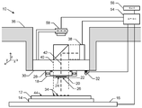
전술한 바와 같이, 패터닝된 피쳐는 포토 리소그래피, 나노임프린트 리소그래피, 극 자외선 리소그래피 및 전자 빔 리소그래피 등을 포함하는 다수의 상이한 리소그래피 기술에 의해 형성될 수 있다. 패턴 피쳐는 하부 재료, 막 또는 기판으로 전사된 패턴을 정의하기 위한 에칭 마스크로서 사용된다. 예시적인 나노임프린트 리소그래피 시스템이 도 1에 도시되어 있다. 나노임프린트 리소그래피 시스템(10)은 기판(12) 상에 릴리프 패턴을 형성하는데 사용될 수 있다. 기판(12)은 기판 척(14)에 결합될 수 있다. 도시된 바와 같이, 기판 척(14)은 진공 척이다. 그러나, 기판 척(14)은 진공, 핀-유형, 홈-유형, 정전기, 전자기 및/또는 등등을 포함하지만 이에 한정되지 않는 임의의 척일 수 있다. 예시적인 척은 미국 특허 제6,873,087호에 기재되어 있으며, 이는 본 명세서에서 참조로 통합된다.As discussed above, the patterned features may be formed by a number of different lithographic techniques including photolithography, nanoimprint lithography, extreme ultraviolet lithography, and electron beam lithography. The pattern feature is used as an etch mask to define a pattern transferred to the underlying material, film or substrate. An exemplary nanoimprint lithography system is shown in Fig. The
기판(12) 및 기판 척(14)은 스테이지(16)에 의해 더 지지될 수 있다. 스테이지 16은 x, y 및 z 축을 따라 병진 및/또는 회전 운동을 제공할 수 있다. 스테이지(16), 기판(12) 및 기판 척(14)은 또한 베이스(미도시) 상에 위치될 수 있다.The
템플릿(18)이 기판(12)으로부터 이격되어 있다. 템플릿(18)은 제1 측면 및 제2 측면을 갖는 본체를 포함할 수 있으며, 한 측면은 기판(12)을 향해 그로부터 연장하는 메사(20)를 갖는다. 메사(20)는 패터닝 표면(22)을 그 위에 가질 수 있다. 또한, 메사(20)는 몰드(20)로 지칭될 수 있다. 대안적으로, 템플릿(18)은 메사(20) 없이 형성될 수 있다.The
템플릿(18) 및/또는 몰드(20)는 융합 실리카, 석영, 실리콘, 유기 폴리머, 실록산 폴리머, 붕규산 유리, 플루오로카본 폴리머, 금속, 경화된 사파이어 및/또는 등등을 포함하는, 그러나 이들에 한정되지 않는 재료로 형성될 수 있다. 도시된 바와 같이, 패터닝 표면(22)은 복수의 이격된 리세스(24) 및/또는 돌출부(26)에 의해 한정된 피쳐를 포함하지만, 본 발명의 실시예는 이러한 구성(예로서, 평면 표면)에 제한되지 않는다. 패터닝 표면(22)은 기판(12) 상에 형성될 패턴의 기초를 형성하는 임의의 원래 패턴을 정의할 수 있다. 템플릿(18)은 척(28)에 결합될 수 있다. 척(28)은 진공, 핀-유형, 홈-유형, 정전, 전자기 및/또는 다른 유사한 척 유형으로 구성될 수 있지만, 이에 한정되는 것은 아니다. 또한, 척(28)은 임프린트 헤드(30)에 결합될 수 있으며, 임프린트 헤드는 차례로 척(28), 임프린트 헤드(30) 및 템플릿(18)이 적어도 z-축 방향으로 이동 가능하도록 브릿지(36)에 이동 가능하게 결합될 수 있다.The
나노임프린트 리소그래피 시스템(10)은 유체 분배 시스템(32)을 더 포함할 수 있다. 유체 분배 시스템(32)은 기판(12) 상에 성형 가능한 재료(34)(예로서, 중합 가능한 재료)를 피착시키는데 사용될 수 있다. 성형 가능한 재료(34)는 적하 분배(drop dispense), 스핀 코팅, 딥 코팅, 화학 기상 증착(CVD), 물리 기상 증착(PVD), 박막 피착, 후막 피착 및/또는 등등과 같은 기술을 사용하여 기판(12) 상에 위치될 수 있다. 성형 가능한 재료(34)는 설계 고려 사항에 따라 몰드(22)와 기판(12) 사이에 원하는 체적이 한정되기 전 및/또는 후에 기판(12) 상에 배치될 수 있다. 예로서, 성형 가능한 재료(34)는 미국 특허 제7,157,036호 및 미국 특허 제8,076,386호에 기술된 바와 같은 단량체 혼합물을 포함할 수 있으며, 이들 모두는 본원에 참고로 포함된다.The
도 1 및 도 2를 참조하면, 나노임프린트 리소그래피 시스템(10)은 경로(42)를 따라 에너지(40)를 지향시키는 에너지 소스(38)를 더 포함할 수 있다. 임프린트 헤드(30) 및 스테이지(16)는 경로(42)와 중첩되게 템플릿(18) 및 기판(12)을 위치시키도록 구성될 수 있다. 카메라(58)가 마찬가지로 경로(42)와 중첩하여 위치될 수 있다. 나노임프린트 리소그래피 시스템(10)은 스테이지(16), 임프린트 헤드(30), 유체 분배 시스템(32), 소스(38) 및/또는 카메라(58)와 통신하는 프로세서(54)에 의해 조절될 수 있으며 메모리(56)에 저장된 컴퓨터 판독 가능 프로그램상에서 작동할 수 있다.Referring to Figures 1 and 2, the
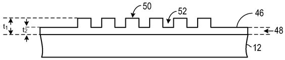
임프린트 헤드(30), 스테이지(16) 또는 둘 모두는 몰드(20)와 기판(12) 사이의 거리를 변화시켜 성형 가능한 재료(34)로 채워지는 그들 사이의 원하는 체적을 한정한다. 예로서, 임프린트 헤드(30)는 몰드(20)가 성형 가능한 재료(34)와 접촉하도록 템플릿(18)에 힘을 가할 수 있다. 원하는 체적이 성형 가능한 재료(34)로 채워진 후, 소스(38)는 성형 가능한 재료(34)가 응고 및/또는 가교 결합되어 기판(12)의 표면(44) 및 패터닝 표면(22)의 형상에 합치됨으로써 기판(12) 상의 패터닝된 층(46)을 형성하게 하도록, 에너지(40), 예를 들어, 자외선 방사선을 생성한다. 패터닝된 층(46)은 잔여 층(48) 및 돌출부(50) 및 후퇴부(52)로 도시된 복수의 피쳐를 포함할 수 있으며, 돌출부(50)는 두께 t1를 가지고 잔여 층은 두께 t2를 갖는다.The
전술한 시스템 및 프로세스는 미국 특허 제6,932,934호, 미국 특허 제7,077,992호, 미국 특허 제7,179,396호 및 미국 특허 제7,396,475호에 언급된 임프린트 리소그래피 프로세스 및 시스템에 추가로 채용될 수 있으며, 이들 모두는 그 전체가 참고 문헌으로 포함된다.The above-described systems and processes may additionally be employed in the imprint lithography processes and systems mentioned in U.S. Patent Nos. 6,932,934, 7,077,992, 7,179,396 and 7,396,475, all of which are incorporated herein by reference in their entirety Are included as references.
후속하여, 패터닝된 층(46)의 패턴에 대응하는 릴리프 이미지를 기판(12)으로 전사하기 위해, 기판(12) 및 패터닝된 층(46)은 에칭 프로세스와 같은 추가적인 프로세스를 거친다. 이렇게 패터닝된 기판(12)은 그후 예로서 산화, 막 형성, 피착, 도핑, 평탄화, 에칭, 레지스트 제거, 다이싱, 본딩 및 패키징 등을 포함하는 디바이스 제조를 위한 공지된 단계 및 프로세스를 추가로 거치게 된다. 유사하게, 광학 리소그래피, 포토 리소그래피, 극 자외선 리소그래피 및 전자 빔 리소그래피 등과 같은 다른 방법 또는 기술에 의해 패터닝된 기판은 마찬가지로 처리되어 기능적 디바이스를 산출할 수 있다.Subsequently, the
현재, 많은 첨단 반도체 디바이스는 100nm 미만의 피쳐 치수를 갖는 고립 및 밀집 피쳐 모두의 패터닝을 필요로 할 수 있다. 본 명세서에 사용될 때, "피쳐 치수" 또는 "피쳐 크기"라는 용어는 패터닝된 피쳐의 가장 좁은 측방향 치수, 예로서 패터닝된 피쳐가 그 폭보다 큰 길이를 갖는 피쳐 폭을 지칭한다. 예로서, 폭이 50nm이고 길이가 5 미크론인 라인 피쳐는 50nm의 피쳐 치수 또는 피쳐 크기를 갖는 것으로 간주된다. 패터닝된 피쳐의 두께(즉, 높이)는 제거하고자 하는 하부 재료, 막 또는 기판의 양, 즉, 달성될 원하는 에칭 깊이 및 하부 재료, 막 또는 기판에 대한 레지스트의 에칭 내성의 선택성에 의해 지정된다. 이전 세대의 리소그래피 기술에서 피쳐 치수가 100nm보다 클 때 밀집 라인 패턴과 같은 종횡비가 5:1 이상인 피쳐를 만들 수 있다(종횡비는 피쳐 폭에 대한 피쳐 높이의 비율로서 정의됨). 예로서, 500nm 라인은 실리콘 이산화물, 실리콘 질화물, 실리콘 산질화물, 폴리실리콘, 금속, 예컨대 탄탈, 텅스텐, 크롬 및 알루미늄 및 금속 실리사이드와 같은 하부 재료에 패턴을 에칭하기에 충분한 5:1의 종횡비에 해당하는 2.5 미크론의 두께(즉, 높이)를 가질 수 있다.Currently, many advanced semiconductor devices may require patterning of both isolated and dense features with feature dimensions less than 100 nm. As used herein, the term "feature dimension" or "feature size" refers to the narrowest lateral dimension of the patterned feature, e.g., feature width where the patterned feature has a length greater than its width. By way of example, a line feature with a width of 50 nm and a length of 5 microns is considered to have a feature dimension or feature size of 50 nm. The thickness (i.e., height) of the patterned feature is specified by the amount of underlying material, film, or substrate to be removed, i.e., the desired etch depth to be achieved and the selectivity of the etch resistance of the resist to the underlying material, film, or substrate. In previous generation lithography techniques, a feature with an aspect ratio equal to or greater than 5: 1 can be created (where the aspect ratio is defined as the ratio of the feature height to the feature width) such that the feature dimension is greater than 100 nm. By way of example, a 500 nm line corresponds to an aspect ratio of 5: 1 sufficient to etch a pattern into underlying material such as silicon dioxide, silicon nitride, silicon oxynitride, polysilicon, metals such as tantalum, tungsten, chromium and aluminum and metal silicide Lt; / RTI > thickness (i. E., Height).
포토 리소그래피 응용에서, 이미징된 포토레지스트의 최대 두께는 일반적으로 2개의 방정식에 의해 결정된다. 첫 번째는 현상 중에 레지스트에 가해지는 힘을 나타낸다. 즉, 노광 후, 레지스트는 광이 레지스트 표면 상에 충돌하는 위치의 레지스트 재료를 선택적으로 제거하는(포지티브 작용 레지스트의 경우) 또는 광이 레지스트 표면 상에 충돌하는 위치의 레지스트 재료를 선택적으로 남기는(네거티브 작용 레지스트의 경우) 현상제 용액 내에 배치되게 된다. 그런 다음, 이런 현상 단계 후에 물 헹굼 및 그 후의 최종 건조 단계가 후속된다. 그러나, 건조 단계 동안 물의 제거는 인접한 레지스트 피쳐들 사이에 모세관 응력 σ를 부여하고, 이는 제1 수학식(수학식 1)에 의해 기술된다:In photolithographic applications, the maximum thickness of the imaged photoresist is generally determined by two equations. The first shows the force applied to the resist during development. That is, after exposure, the resist may be selectively removed (in the case of a positive working resist) at the location where the light impinges on the surface of the resist, or selectively in a position where the light strikes the resist surface In the case of a working resist). This development step is followed by a water rinse followed by a final drying step. However, the removal of water during the drying step imparts a capillary stress? Between adjacent resist features, which is described by the first equation (1): < RTI ID = 0.0 >

여기서, γ는 표면 장력이고, θ는 레지스트 피쳐 상단의 물의 접선 각도, H/W는 종횡비(높이 대 폭)이며, S1은 레지스트 패턴 사이의 간격이다. 수학식 1에서 알 수 있듯이, 피쳐 크기(W)가 작을수록 레지스트 패턴이 받는 모세관 응력이 더 높아진다.Here, γ is the surface tension, θ is the tangential angle of water at the top of the photoresist feature, H / W aspect ratio (height to width), S 1 is a distance between the resist patterns. As can be seen from Equation (1), the smaller the feature size (W), the higher the capillary stress the resist pattern receives.
피쳐가 직립 상태로 유지되는지 또는 피쳐에 부여된 응력이 일반적으로 피쳐 압궤라고 지칭되는 영구적인 굴곡을 일으키는지 여부는 레지스트 재료의 기계적 강성도에 의존한다. 건조 스테이지에서 모세관 응력으로 인해 야기되는 피쳐 압궤 외에도, 마찬가지로 습식 세정과 같은 다른 프로세스로 인해 피쳐가 굴곡되고, 맞닿고, 압궤되게 하는 힘이 생길 수 있다. 인접한 피쳐에서의 증기 제거는 유사한 효과를 갖는다. 나노임프린트 리소그래피의 경우, 레지스트를 경화한 후 템플릿과 웨이퍼를 분리하는 동안 겪게 되는 측방향 방향 힘으로 인해 피쳐 압궤가 발생할 수도 있다. 피쳐의 편향은 제2 수학식(수학식 2)에 의해 설명될 수 있다:Whether the feature remains in an upright state or the stress imparted to the feature causes permanent bending, commonly referred to as a feature crush, depends on the mechanical stiffness of the resist material. In addition to the feature crushing caused by capillary stress in the drying stage, another process, such as wet scrubbing, may also cause a force to bend, abut, and crush the feature. Steam removal in adjacent features has a similar effect. In the case of nanoimprint lithography, feature crushing may occur due to the lateral forces experienced during the separation of the template and the wafer after curing the resist. The deflection of the feature can be described by the second equation (Equation 2): < EMI ID =

여기에서 δ은 피쳐의 측방향 이동의 양, F는 부여된 힘(예를 들어, 모세관 응력 σ 또는 기타 힘), E는 영 모듈러스, H는 피쳐의 높이 그리고, wl는 피쳐의 폭이다. 이 수학식에서 알 수 있듯이, 종횡비, H/wl 및 레지스트 막의 기계적 강성도(영 모듈러스)(E)는 모두, 피쳐 압궤에 중요한 역할을 한다. 따라서 임의의 주어진 종횡비에 대해 피쳐 굴곡의 양은 재료의 기계적 강성도에 반비례한다.Where E is the amount of lateral movement of the feature, F is the applied force (e.g., capillary stress, or other force), E is the Young modulus, H is the height of the feature, and wl is the width of the feature. As this can be seen in a mathematical formula, the aspect ratio, the mechanical stiffness H / l w and the resist film (Young's modulus) (E) are all, play a major role in the feature collapse. Thus, for any given aspect ratio, the amount of feature bending is inversely proportional to the mechanical stiffness of the material.
그러나 피쳐 크기가 100nm 미만의 치수로 줄어들면 대략 5:1 이상의 종횡비가 더 이상 유지될 수 없다. 이는 레지스트 재료의 기계적 특성이 그러한 더 작은 치수에서 그 벌크 특성으로부터 벗어나기 시작하기 때문이다. 일 예로서, 도 3은 50nm 미만의 폭을 갖는 라인 피쳐를 갖는 폴리스티렌으로 형성된 박막의 예측된 영 모듈러스를 플롯팅한다. 도시된 바와 같이, 피쳐의 실제 영 모듈러스(플롯 라인(304))는 라인 폭이 50nm 아래로 떨어짐에 따라 벌크 값 영 모듈러스(플롯 라인(302))로부터 벗어남으로써 피쳐의 실제 영 모듈러스는 30nm에서 벌크 값 영 모듈러스의 약 60 % 및 20nm에서 벌크 값 영 모듈러스의 40 % 미만까지 떨어진다. 결과적으로, 50nm 미만의 레지스트 피쳐에 대해, 보다 합리적인 가공 기대치는 사용된 리소그래피 방법에 관계없이 2.5:1 이하의 종횡비이다. 또한 라인 크기가 25nm 미만으로 떨어지면, 심지어 2.5:1의 종횡비도 과제가 될 수 있다.However, if the feature size is reduced to a dimension of less than 100 nm, an aspect ratio of about 5: 1 or more can no longer be maintained. This is because the mechanical properties of the resist material begin to deviate from its bulk properties at such smaller dimensions. As an example, FIG. 3 plots the predicted zero modulus of a thin film formed of polystyrene having a line feature with a width less than 50 nm. As shown, the actual zero-modulus of the feature (plot line 304) is shifted away from the bulk value zero modulus (plot line 302) as the line width falls below 50 nm, Value to about 60% of the Young's modulus and less than 40% of the bulk value Young's modulus at 20 nm. As a result, for resist features of less than 50 nm, a more reasonable processing expectation is an aspect ratio of 2.5: 1 or less, regardless of the lithography method used. Also, if the line size falls below 25 nm, even an aspect ratio of 2.5: 1 can be a challenge.
이러한 작은 피쳐 크기(즉, 50nm 미만)에 요구되는 필요한 재료 강성도에 대한 지침은 도 3 및 수학식 2에 도시된 바와 같은 라인 플롯으로부터 외삽될 수 있다. 재료의 벌크 영 모듈러스가 1GPa 정도이지만 30nm 피쳐 크기에서 벌크 값의 약 60 %로 떨어져, 약 0.60GPa의 이러한 피쳐에 대한 실제 또는 유효 영 모듈러스를 생성하는 경우를 고려한다. 본원에서 사용되는 "유효 영 모듈러스" 또는 "Eeff"이라는 용어는 50nm 미만의 피쳐 크기에서 피쳐의 폭을 고려한 영 모듈러스 값을 의미하며, 그래서, 이는 이러한 피쳐를 형성하는 데 사용된 재료의 벌크 값 영 모듈러스의 약간 더 적은 백분율이다. 그 다음에, 임의의 피쳐의 부여된 편향이 피쳐의 종횡비의 3승에 비례하고 영 모듈러스에 반비례한다는 것을 설명하는 수학식 2를 적용함으로써, 주어진 원하는 종횡비에 대한 필요한 효과적인 유효 영 모듈러스를 설명하는 플롯이 도출될 수 있다. 그러한 플롯의 예가 도 4에 도시되어 있다. 여기서, 플롯(402)은 종횡비의 함수로서 유효 영 모듈러스의 거동을 도시한다. 종횡비가 2.5:1인 경우, 30nm 피쳐가 ~ 0.60GPa의 유효 영 모듈러스에 의해 지지될 수 있다. 그러나 3.5:1의 종횡비가 바람직한 경우, 유효 영 모듈러스는 ~1.65GPa까지 증가해야한다. 유사하게, 5:1의 종횡비가 바람직한 경우, 유효 영 모듈러스는 5GPa 바로 아래까지 증가되면 된다. 실제 유효 영 모듈러스는 실제 재료 및 피쳐의 크기에 따라 물론 변경될 수 있다. 그러나 어떤 경우에도 피쳐의 편향은 피쳐의 종횡비의 3승에 항상 비례하고 유효 영 모듈러스에 반비례한다.The guidelines for the required material stiffness required for such small feature sizes (i.e., less than 50 nm) can be extrapolated from the line plots as shown in FIG. 3 and FIG. Consider the case where the material's bulk Young's modulus is on the order of 1 GPa but is about 60% of the bulk value at 30 nm feature size, producing a real or effective Young's modulus for this feature of about 0.60 GPa. The term " effective Young modulus "or" Eff, " as used herein, refers to a zero modulus value that takes into account the width of a feature at a feature size of less than 50 nm, It is a slightly lesser percentage of zero modulus. Then, by applying
그러나, 종횡비가 2.5:1 이하로 감소함에 따라, 하부 재료를 성공적으로 패터닝하기 위해 패터닝된 레지스트 층 자체를 사용하는 것은 불가능하지는 않지만 매우 어려워진다. 따라서, 하부 재료 또는 기판을 에칭하기 위해 사용되는 건식 에칭 플라즈마 기반 프로세스에 견딜 수 있는 보다 복잡한 구조가 일반적으로 사용된다. 이러한 구조 또는 "스택"은 일반적으로 두 개 이상의 재료로 구성되며 때때로 "다층 스택"이라고도 한다. 예로서, 다층 스택은 패터닝된 레지스트 층, 패터닝된 레지스트 층 아래의 스핀-온 글래스(SOG)와 같은 하드 마스크 층 및 예로서, 기판에 적용된 스핀 온 카본(SOC) 층 또는 다른 탄소 기반 유사 재료와 같은 탄소 층 같은 하부 막을 포함할 수 있다. 탄소 기반 재료 이외에, 하부 막은 우수한 에칭 내성을 제공하는 실리콘 또는 다른 무기 원소를 함유할 수 있다. 선택적으로, 하부 막 위에 적용된 하드 마스크 층이 하드 마스크와 하부 막 사이에 양호한 에칭 선택성을 제공하도록 적절히 선택되는 한, 하부 막은 전체적으로 무기질일 수 있다. 일 예로서, 하부 막은 실리콘 이산화물일 수 있고, 하드 마스크는 크롬일 수 있다. 탄소 기반 막을 포함하는 이러한 하부 막은 스퍼터 피착 및 화학 기상 증착 및 전자 빔 증발을 포함하는 진공 기반 방법을 사용하여 스핀-온 또는 적용될 수 있다. SOC의 경우, SOC 층은 일반적으로 높은 중량 %의 탄소를 함유하여, 에칭 내성적 및 기계적으로 강성화되게 한다. 예를 들면, 노볼락 레지스트 같은 다른 유기-기반 탄소 재료에 대하여, 하드 마스크 층을 적용하기 전에 베이크 프로세스를 통해 치밀화, 에칭 내성 및 강성도를 증가시키는 감열성 가교 결합 성분을 첨가할 수 있다. 탄소 층으로 전사된 패턴 피쳐가 기판 내로의 후속 패턴 전사에 사용될 것이기 때문에 탄소 층의 에칭 내성 및 강성도 모두가 중요하다.However, as the aspect ratio decreases to less than 2.5: 1, it is not impossible, but very difficult, to use the patterned resist layer itself to successfully pattern the underlying material. Thus, more complicated structures that are capable of withstanding dry etch plasma based processes used to etch underlying materials or substrates are commonly used. Such a structure or "stack" is generally composed of two or more materials and is sometimes referred to as a "multi-layer stack ". By way of example, the multilayer stack may include a patterned resist layer, a hard mask layer such as spin-on glass (SOG) under the patterned resist layer, and a spin-on-carbon (SOC) Such as a carbon layer. In addition to carbon-based materials, the underlying film may contain silicon or other inorganic elements that provide good etch resistance. Optionally, the bottom film may be entirely inorganic, so long as the hard mask layer applied over the bottom film is properly selected to provide good etch selectivity between the hard mask and the underlying film. As an example, the bottom film may be silicon dioxide and the hard mask may be chrome. Such a bottom layer comprising a carbon-based film can be spun-on or applied using vacuum-based methods including sputter deposition and chemical vapor deposition and electron beam evaporation. In the case of SOC, the SOC layer generally contains a high percentage by weight of carbon, making it etch resistant and mechanically stiff. For other organic-based carbon materials, such as, for example, novolak resists, a thermosensitive cross-linking component may be added that increases densification, etch resistance and stiffness through a bake process prior to application of the hardmask layer. Both the etch resistance and stiffness of the carbon layer are important because the pattern feature transferred to the carbon layer will be used for subsequent pattern transfer into the substrate.
이러한 다층 스택 솔루션은 다층 스택이 피착되는 표면이 평면이 아닌 상황을 제외하면 충분히 합리적으로 양호하게 작동한다. 사실, 어떠한 표면도 완벽하게 평탄하지 않으며, SOC와 같은 스핀 온 막은 기판의 기본 토포그래피를 완벽하게 평탄화시키지 못하며, 평탄화를 위한 성공적인 진공 기반 응용 방법도 아니라는 것이 잘 알려져 있다. 특히 주목되는 두 가지 비-평면 상황이 있다. 첫 번째는 "단파장" 평면 편위가 표면 상에 발생하는 경우(즉, 나노미터 또는 미크론의 스케일을 초과하여 발생하는 편위가 그러한 짧은 스케일에서 작은 평면 섭동을 야기하는 경우)이다. 임프린트 리소그래피 응용의 경우, 이는 잔여 층 두께의 작은 변화를 초래할 것이고, 이는 차례로 패턴 전사 후에 임계 치수(CD) 균일성 에러를 생성한다. 모든 유형의 광학 리소그래피에서, 스캐너는 그러한 짧은 스케일에 대한 높이 변화를 보정할 수 없으며, 결과적 평탄성의 편차는 스캐너 또는 스텝퍼에 대한 초점 심도 예산에 영향을 미치고, 이에 따라 마찬가지로 레지스트 이미징 동안 유사한 CD 에러를 도입한다.This multi-layer stack solution works reasonably well except in situations where the surface on which the multi-layer stack is deposited is not planar. In fact, it is well known that no surface is perfectly smooth, and spin-on films such as SOC do not completely flatten the substrate's topography and are not successful vacuum-based applications for planarization. There are two non-planar situations of particular interest. The first is when "short wavelength" planar deviations occur on the surface (i.e., deviations occurring in excess of the nanometer or micron scale cause small planar perturbations at such short scales). In the case of imprint lithography applications, this will result in small changes in the residual layer thickness, which in turn produces critical dimension (CD) uniformity errors after pattern transfer. In all types of optical lithography, the scanner can not compensate for height variations for such short scales, and deviations in the resultant planarity affect the depth of focus budget for the scanner or stepper, thereby similarly producing similar CD errors during resist imaging .
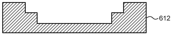
토포그래피 변화가 기판의 수십 미크론 또는 심지어 수 밀리미터를 초과하여 존재할 때 두 번째 더 어려운 문제가 발생한다. 이러한 유형의 토포그래피의 예가 도 5a에 도시되어 있다. 도 5a는 토포그래피가 상승되거나 하강되는 큰 면적(수 미크론 또는 수 밀리미터 초과)을 갖는 기판(512)을 도시한다. 이러한 토포그래피 변화는 수 나노미터에서 수십 또는 심지어 수백 나노미터까지 어디에든 이를 수 있다. 수백 나노미터 수준의 토포그래피는 심각한 이미징 문제를 생성한다. 통상적으로 화학 기계 연마(CMP) 단계는 그러한 토포그래피 변화를 감소시키기 위해 적용된다. 그러나 CMP 단계로도 최종 토포그래피는 여전히 수십 나노미터의 변화를 가질 수 있다. 광학 리소그래피의 경우, 스캐너는 큰 면적에 걸친 이러한 토포그래피 변화의 일부를 보상할 수 있다. 그러나 전이 영역에서 초점 심도 문제가 심각해지고 이미징에 심각한 영향을 준다. 결과적으로, 디바이스 제조자는 관심 수준에 맞는 정확한 패턴을 생성하기 위해 두 개의 상이한 마스크를 사용하여 두 번의 별도 노광을 해야 할 수밖에 없으므로 디바이스 제조 프로세스에 상당한 비용이 추가된다. 나노임프린트 리소그래피의 경우, 이러한 토포그래피 문제는 마찬가지로 심각한 결과를 가질 수 있다. 즉, 평탄성의 큰 편위는 전술한 바와 같이 임계 치수(CD) 균일성에 영향을 미치는 잔여 층 두께 변화를 야기할 수 있다. 느린 레지스트 충전(공구 처리량 및 따라서 소유 비용에 영향을 미침) 및 일부 경우에 제조되는 디바이스의 기능성에 영향을 줄 수 있는 비 충전 결함 같은 더 근본적인 문제도 관찰될 수 있다.The second more difficult problem arises when the topography change is present on the substrate in the tens of microns or even in excess of a few millimeters. An example of this type of topography is shown in FIG. 5A. 5A shows a
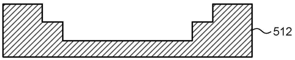
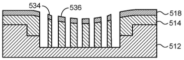
전사된 피쳐에서 임계 치수 변동성의 결과적인 해로운 영향을 갖는 이러한 토포그래피에 대한 패턴 전사 체계가 도 5a 내지 도 5h에 도시되어 있다. 도 5a에 도시된 바와 같이, 기판(512)은 큰 면적(예로서, 수 미크론 이상)에 걸쳐 연장되는 연관된 토포그래피를 갖는다. 도 5b에 도시된 바와 같이, SOC 층(514)은 기판(512) 상에 피착되어 있고, 표면(516)은 기판(512)의 하부 토포그래피와 연계된 토포그래피 상에서 취해진다. 즉, SOC 층(514)의 표면(516)의 토포그래피는 기판(512)의 하부 토포그래피에 대응한다. SOC 층(514)의 평탄성 변화는 하부 기판(512)의 것과 같이 두드러지지는 않지만 그럼에도 불구하고 이들은 평탄성 변화를 갖는 표면을 계속 나타낸다. 도 5c에서, 하드 마스크 층(518)은 SOC 층(514) 위에 피착되어 있다. 특히, 하드 마스크 층(518)은 SOC 층(514)의 토포그래피와 일치하는 표면(520)을 가지므로, 하드 마스크 층(518)은 SOC 층(514)의 표면(516)과 동일한 평탄성 변화를 갖는 표면(520)을 나타낸다. 도 5d에서, 균일한 피쳐(524 및 526)를 갖는 패터닝된 층(522)은 나노임프린트 프로세스에 의해 하드 마스크 층(518) 위에 적용된다. 하드 마스크 층(518)의 토포그래피 변화 때문에, 패터닝된 층(522)은 불균일한 잔여 층(528)을 갖는다. 도 5e는 하드 마스크 층(518)에 피쳐(534, 536)를 형성하기 위해 하드 마스크 층(518)으로의 패터닝된 층(522)의 결과적 패턴 전사를 도시한다. 잔여 층 비-균일성 때문에, 잔여 층(525)을 제거하기 위한 에칭 시간이 잔여 층(528)의 변화하는 두께의 함수로서 변하므로, 가장 작은 패터닝된 전사된 피쳐(534 및 536)("임계 피쳐"라고도 함)의 임계 치수(CD)는 더 이상 균일하지 않다. 패턴 전사가 도 5f에 도시된 바와 같이 SOC 층(514) 내로 계속 진행됨에 따라, 피쳐(534 및 536)의 비-균일성이 따라서 이전된다. 마지막으로, 하부 기판(512)이 에칭되고 남아있는 SOC 및 레지스트 재료가 제거되고(도 5g 내지 도 5h), 비-균일성을 갖는 최종 기판 피쳐(544 및 546)는 잔여 층(522)의 에칭 동안 도입된 비-균일성에 상응한다. 전술한 바와 같이, 이러한 임계 치수 비-균일성은 나노임프린트 리소그래피에 한정되지 않는다. 또한 토포그래피의 변화는 광학 및 극 자외선(EUV) 리소그래피에서 초점 심도에 영향을 미치며 마찬가지로 노광 프로세스 동안 도입되는 임계 피쳐 비-균일성을 초래한다.The pattern transfer scheme for such topography with the detrimental effect of critical dimension variability in transferred features is shown in Figures 5A-5H. As shown in FIG. 5A, the
대조적으로, 본 발명은 (1) 패터닝된 피쳐가 임계 피쳐의 비-균일성 에러 또는 다른 결함 문제를 발생시키거나 패터닝된 피쳐 모두를 형성하기 위해 다수의 리소그래피 단계의 사용을 필요로 하지 않고 쉽게 정의될 수 있도록 평면 표면을 생성하고, (2) 전사 에칭 후에 여전히 양호한 에칭 내성을 가지며 높은 종횡비 피쳐(종횡비 2.5:1 이상을 갖는 피쳐)가 표준 처리 조건 하에서 굴곡되거나 흔들리거나 압궤되지 않도록 기계적으로 안정한 구조를 초래하는 솔루션을 제공한다. 본 명세서에서 더 상세히 설명되는 바와 같이, 이는 (1) 토포그래피 변화를 포함하는 기판 상에 예로서 SOC 층 같은 탄소 막 층을 먼저 적용하고, (2) 탄소 층의 상부에 얇은 유기 평탄화 막을 적용하고, (3) 탄소 층의 상부에 하드마스크 층을 적용하고, (4) 예로서, 임프린트 또는 광학 리소그래피 프로세스에 의해 하드 마스크 층 위에 패터닝된 층을 형성하며, (1) 내지 (4) 단계에서, 그에 의해, 탄소 막, 평탄화 막, 하드 마스크 및 패터닝된 층의 다층 스택을 형성하고, (5) 패터닝된 층의 패턴을 다층 스택으로 그리고 그후 하부 기판으로 전사하는 것에 의해 달성된다. 특정 예에서, 다층 스택은 전형적인 처리 조건 하에서 2.5:1 이상의 종횡비에서 50nm 이하의 피쳐를 유지할 수 있는 복합 유효 기계적 강성도(Eeff)를 갖는다. 이러한 프로세스의 일 실시예는 다음과 같이 도 6a 내지 도 6i에 상세히 설명된다.In contrast, the present invention provides a lithographic apparatus that (1) can be easily defined without requiring the use of multiple lithography steps to produce patterned features that produce non-uniformity errors or other defect problems of critical features or both patterned features (2) a mechanically stable structure that still has good etch resistance after transfer etch and a high aspect ratio feature (features with an aspect ratio of 2.5: 1 or more) is not bent, shaken or crushed under standard processing conditions ≪ / RTI > As will be described in greater detail herein, this is accomplished by (1) first applying a carbon film layer, such as, for example, an SOC layer, onto a substrate comprising a topographical change, (2) applying a thin organic planarizing film on top of the carbon layer (3) applying a hard mask layer on top of the carbon layer, and (4) forming a patterned layer on the hard mask layer by, for example, an imprint or optical lithography process, Thereby forming a multilayer stack of a carbon film, a planarizing film, a hard mask and a patterned layer, and (5) transferring the pattern of the patterned layer to a multilayer stack and then to a lower substrate. In certain instances, the multilayer stack has a composite effective mechanical stiffness (Eeff) that can maintain a feature of 50 nm or less at an aspect ratio of 2.5: 1 or greater under typical processing conditions. One embodiment of this process is described in detail in Figures 6A-6I as follows.
도 6a를 참조하면, 기판(612)은 도 5a의 기판(512)과 동일한 비-평면 토포그래피를 갖는다. 도 6b에서, SOC 층(614)은 기판(612) 상에 피착되어, SOC 층(614)의 표면(616)이 도 5b와 유사한 기판(612)의 하부 토포그래피와 연관된 토포그래피를 취한다. 그 다음, 도 6c에 도시된 바와 같이, 평탄화 재료가 SOC 층(614) 위에 적용되어 평탄화 층(618)을 형성한다. 특히, 평탄화 층(618)의 상부 표면(620)은 사실상 평평하고, 즉, SOC 층(614)의 표면(616)의 하부 토포그래피와 연관된 어떠한 토포그래피도 취하지 않는다. 따라서, 예로서 광학 또는 임프린트 리소그래피를 사용하여 SOC 층(614) 위에 패터닝되는 피쳐는 전술한 바와 같이 표면 토포그래피 변화를 초래하는 임계 치수 변화 또는 다른 단점없이 전사될 수 있다. 도 6d 내지 도 6i는 추가 프로세스 단계를 나타낸다. 도 6d에서, 하드 마스크 층(622)은 평탄화 층(618) 위에 피착되고, 도 6e에서, 피쳐(624, 626)를 가지며 잔여 층(628)을 갖는 패터닝된 층(620)은 하드 마스크 층(622) 위에 형성된다. 도 6f는 피쳐(634 및 636)를 형성하기 위해 하드 마스크 층(622)으로의 패턴의 전사 에칭이 후속되는 잔여 층(628)의 균일한 에칭의 결과를 나타낸다. 다음으로, 도 6g에서, 패턴은 평탄화 층(618) 및 SOC 층(614) 모두에 에칭된다. 평탄화 층(618) 및 SOC 층(614)은 일반적으로 모두 유기성이기 때문에, 두 재료를 에칭하는데 사용되는 에칭 화학제는 동일할 수 있으며, 일반적으로 헬륨 또는 아르곤 같은 추가 가스와 조합된 산소, 일산화탄소, 이산화탄소와 같은 주요 에칭제 가스로 구성된다. 마지막으로, 도 6h 내지 도 6i에 도시된 바와 같이, 패턴은 기판(612)으로 전사되어 플라즈마 에칭 또는 습식 에칭 중 어느 하나에 의해 제거된 나머지 층과 함께 최종 피쳐(644 및 646)를 형성한다.Referring to FIG. 6A, the
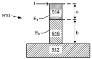
전술한 프로세스의 중요점은 도 6g에 도시된 패턴 전사 단계 후에, 기판(612)에 부착된 SOC의 비교적 두꺼운 층(SOC 층(614))이 남는다는 것이다. 본 명세서에 추가로 설명된 바와 같이, 기판(612)에 인접한 이 SOC 층(614)은 에칭된 피쳐(634 또는 636)에 기계적 강성도를 제공하여, 에칭된 피쳐의 굴곡이 최소화되게 하며, 이는 기판에 인접하게 위치된, 기계적 강성도가 훨씬 적은 평탄화 층을 갖는 경우와는 대조적이다. 또한, SOC 층(614)은 기판 내로의 후속 에칭을 위한 양호한 에칭 보호를 제공한다. 이는 평탄화 층(616)이 SOC 층(614)에 대해 등가의 에칭 내성을 갖지 않을 수도 있기 때문에 중요할 수 있다. 특정 경우에, 평탄화 층(616)은 SOC 층(614)에 비해 0 % 내지 30 %의 에칭 내성 강하를 가질 수 있다. 따라서, 소정 양태에서, 높은 종횡비의 구조의 제공시, SOC 및 평탄화 재료의 증착의 순서, 즉, 먼저 적용된 SOC 층을 적용한 후 평탄화 층을 적용하는 것이 유리하다. 이 방법을 채택함으로써 (1) 하드 마스크 층 및 후속하는 패터닝 층을 적용하기 전에 표면 토포그래피가 평탄화되어, 전사 에칭 동안 임계 치수의 최소 변화를 보장하고, (2) 평탄화 층을 적용하기 전에 SOC 층의 피착은 전체 다층 스택의 에칭 이후의 피쳐의 양호한 기계적 강성도를 보증하여 피쳐 압궤가 회피된다. 이러한 장점은 도 7 및 도 8를 참조하여 더 설명된다.An important point of the above-described process is that after the pattern transfer step shown in FIG. 6G, a relatively thick layer of SOC (SOC layer 614) attached to
도 7은 SOC 층(714)이 기판(712) 상 및 평탄화 층(716) 아래에 적용되는 단일 전사 에칭 피쳐(710)의 단순화된 경우를 도시한다. 설명을 위해, 하드 마스크 층은 그 두께가 평탄화 층(716) 및 SOC 층(714)의 두께에 비해 무시할 수 있기 때문에 도시되지 않는다. 이 경우, 피쳐(710)의 상부에 적용된 측방향 힘(f)의 적용에 의해 야기된 피쳐(710)의 편향은 더 이상 단순히 영 모듈러스에 반비례하지 않는다. 대신, 고차 보정 항을 포함하고 다음 수학식(수학식 3)의 형태를 취한다.Figure 7 illustrates a simplified case of a single
![]()
![]()
여기서, δ는 피쳐의 측방향 편향의 양(또는 이동), f는 부여된 힘, I은 관성 모멘트, a는 SOC 층(714)의 두께(또는 높이), Ea는 SOC 층(714)의 영 모듈러스, b는 평탄화 층(716)의 두께(또는 높이)이고, Eb는 평탄화 층(716)의 영 모듈러스이다. 예시를 위해 Ea가 5GPa로 설정되고 Eb가 1GPa로 설정되므로 Ea와 Eb 사이의 비율은 5이다(즉, Ea/Eb = 5). 총 피쳐 두께(또는 높이)가 a + b = 1이 되도록 정규화되면 편향 δ은 다음 수학식(수학식 4)의 형태를 취한다.Where a is the thickness (or height) of the
![]()
![]()
수학식 4를 사용하여, 피쳐의 상대적인 측방향 편향의 양(또는 "편향 비율")은 복합재 피쳐의 전체 높이(a + b)의 비율로서의 SOC 층의 높이(a)의 함수로서 플롯화될 수 있다. 도 8에서, 플롯(820)은 Ea/Eb가 5와 같은 상황에 대한 편향 비율을 나타낸다. 이 상황에서, 피쳐가 전체적으로 SOC 층(714)으로 구성되어 a의 비율이 1.0과 같으면, 이때, 상대적 편향은 1.0의 최소 값이고, 피쳐가 전체적으로 재료 평탄화 층(716)(즉, 재료 b)으로 구성되어 a의 비율이 0이면 이때, 상대적 편향은 5x 배 초과 또는 5.0이다. 유사하게 플롯(830)은 Ea/Eb가 3과 같은 상황에 대한 편향 비율을 도시한다. 여기서, a의 비율이 1.0이 되도록 피쳐가 SOC 층(714)으로 전체적으로 구성되는 경우, 상대적 편향은 1.0의 최소 값이고, 피쳐가 전체적으로 재료(b)로 구성되어 a 비율이 0인 경우 상대적 편향은 3x 초과 또는 3.0이다.Using
이 편향 비율이 이러한 다층 스택의 재료 조성에 어떻게 영향을 주는지에 대한 예로서, SOC 층이 5의 영 모듈러스를 갖는 플롯(820)의 상황을 가정하면, 평탄화 층은 1의 영 모듈러스를 가지며, Ea/Eb는 5와 같으며, 추가로 5:1의 종횡비가 후속 에칭 단계에 필요하다. 도 4에 도시된 바와 같이, 이런 5:1 종횡비에서 작은 피쳐(예로서, 50nm 미만)를 지지하기 위해서는 5에 가까운 유효 모듈러스가 요구된다. 도 8의 플롯(820)을 다시 참조하면, 100 % SOC 층을 80 % SOC 및 20 % 평탄화 재료로 이루어진 복합재 스택으로 대체함으로써, 전체적으로 100 % SOC 재료로 이루어진 피쳐에 비해 편향 비율의 변화가 단지 3 %만큼 시프트된다는 것을 알 수 있다. 이 예의 SOC 재료가 5의 영 모듈러스를 가지기 때문에, 이때, 이런 3 %의 상대적 편향 비율의 시프트는 복합 재료의 유효 모듈러스를 동일한 3 %만큼 낮추어, 복합 재료에 대한 4.85GPa의 유효 모듈러스를 초래하며, 이는 원하는 5:1 종횡비 피쳐를 지지하기에 전체적으로 충분하다.As an example of how this deflection ratio affects the material composition of such a multilayer stack, assuming the situation of the
이제 동일한 상황에 대해, 피쳐 종횡비 비율과 더불어 토포그래피 변화의 추가적 문제를 추가로 고려한다. 예로서 임계 피쳐가 30nm 폭인 경우, 이때, 5:1 종횡비는 총 복합재 스택이 150nm이어야 한다는 것을 나타낸다. 스택의 20 %가 평탄화 층으로부터 유도되는 경우, 평탄화 층의 두께는 30nm가 될 것이다. 기판의 하부 토포그래피 변화가 30nm보다 작으면, 이때, 20 % 평탄화 층(30nm)은 이런 토포그래피를 평탄화하는데 충분할 것이다. 그러나, 실제로, SOC 막 자체가 먼저 기판 상에 스핀 다운되는 것에 의해 적용되고 그렇게 하는 과정에서 이미 토포그래피 변화의 일부를 감소시킴에 따라 평탄화 상황이 향상된다. 즉, 스핀 온 막은 일반적으로 하부 토포그래피 변화의 약 절반만큼 필요한 평탄화의 양을 감소시킬 수 있다(피쳐 간격에 의존함, 즉, 작은 피쳐 간격(~ 1 미크론 미만)은 큰 피쳐 간격보다 훨씬 효율적으로 평탄화됨). 결과적으로, 30nm의 시작 토포그래피 변화는 전술한 접근법에 의해 쉽게 평탄화될 수 있으며, 약 60nm까지의 시작 토포그래피 변화도 먼저 80 % 스핀-온 SOC 층을 적용한 다음, 20 % 평탄화 막을 적용함으로써 해결될 수 있다.Now, for the same situation, we further consider the additional problem of topographical change along with the aspect aspect ratio. As an example, if the critical feature is 30 nm wide, then a 5: 1 aspect ratio indicates that the total composite stack should be 150 nm. If 20% of the stack is derived from the planarization layer, the thickness of the planarization layer will be 30 nm. If the substrate's underlying topography change is less than 30 nm, then a 20% planarization layer (30 nm) will be sufficient to planarize such topography. However, in practice, the SOC film itself is first applied by spinning down on the substrate, and in the course of doing so, the planarization situation is improved by reducing some of the topographic changes already. That is, spin-on films can generally reduce the amount of planarization required by about half of the bottom-topography variation (depending on feature spacing, i.e., small feature spacing (less than ~ 1 micron) Flattened). As a result, a start topography change of 30 nm can be easily planarized by the approach described above, and a start topography change of up to about 60 nm is also resolved by first applying an 80% spin-on SOC layer and then applying a 20% planarization film .
제2 예로서, 동일한 재료 조건(즉, 영 모듈러스가 5인 SOC 재료 및 영 모듈러스가 1인 평탄화 재료)에 대해 단지 4:1의 작은 피쳐 종횡비가 요구되며, 그 후, 도 5에 도시된 바와 같이, 유효 영 모듈러스는 2.46GPa 만큼 낮을 수 있다. 수학식 2의 연산에 의해, 2의 인자만큼 영 모듈러스를 감소시킴으로써(즉, 5GPa에서 2.46GPa까지), 허용 가능한 편향(d)의 양은 2의 인자만큼 증가된다. 이 경우, 도 8의 플롯(820)을 참조하면, 2의 편향 비율이 수용될 수 있다. 결과적으로, 4:1의 종횡비는 30 %만큼 작은 SOC와 복합 두께의 70%만큼 많은 낮은 모듈러스 평탄화 막으로부터 유래된 피쳐의 복합 두께에 의해 지지될 수 있다.As a second example, a small feature aspect ratio of only 4: 1 is required for the same material conditions (i.e., a SOC material having a Young modulus of 5 and a planarizing material having a Young's modulus of 1) Likewise, the effective Young modulus can be as low as 2.46 GPa. By the operation of equation (2), the amount of allowable deflection (d) is increased by a factor of 2 by decreasing the Young modulus by a factor of two (i.e. from 5 GPa to 2.46 GPa). In this case, referring to the
제3 예에서, 후속 피착된 평탄화 막(716)에 대한 2GPa의 영 모듈러스와 SOC 층(714)을 위한 6GPa의 영 모듈러스를 가정한다. 이 경우 두 막 사이의 영 모듈러스 비율은 3이다(Ea/Eb = 3). 이 상황에 대한 이 예의 편향 비율(도 8, 플롯(830))은 1.0 내지 3.0에서 변한다. 제1 예에서와 같이, 역시 유효 영 모듈러스가 적어도 5 바로 아래이어야 하는 경우에 해당하는 5:1의 피쳐 종횡비를 역시 목적으로 할 수 있다. 플롯(830)에 따르면, 단지 편향 비율을 약 10 %까지 증가시키면서, 복합재 스택의 30 %까지가 이제 평탄화 막(716)으로 구성될 수 있다. 이 예의 SOC 재료가 6의 영 모듈러스를 가지기 때문에, 상대적 편향 비율에서의 10 % 시프트는 유효 모듈러스의 유사한 양만큼의 감소에 대응하고, 5를 훨씬 더 초과한 유효 영 모듈러스를 초래하며, 이는 이전에 언급한 바와 같이 5:1의 종횡비를 완벽하게 지지할 수 있다.In a third example, assume a Young modulus of 2 GPa for the subsequently deposited
제4 예로서, 예 3에서와 동일한 재료 조성을 사용하지만 단지 4:1의 종횡비가 대신 요구되는 경우, 이때, 도 5의 플롯에 따라, 유효 영 모듈러스는 2.46GPa만큼 낮을 수 있다. 영 모듈러스를 2의 인자보다 크게 감소시킴으로써(즉, 6GPa에서 2.46GPa까지 감소), 허용 가능한 편향(d)의 양은 2를 초과한 인자만큼 증가된다. 이 경우, 플롯(830)에 따르면, 2보다 큰 편향 비율이 수용될 수 있고, 결과적으로, 복합재 두께의 약 80 %가 낮은 모듈러스 평탄화 막으로부터 유래될 수 있으며, 20 %만큼 작은 복합 두께가 SOC 막에서 유래될 수 있다. 상당한 양의 평탄화 막이 복합재 스택에 통합될 수 있기 때문에, 고 종횡비 피쳐 구조를 달성하고 수십 나노미터 정도로 하부 토포그래피를 완전히 평탄화 할 수 있는 복합재 스택을 제공하는 두 문제점이 만족스럽게 해결된다.As a fourth example, if the same material composition as in Example 3 is used but only an aspect ratio of 4: 1 is required instead, then according to the plot of FIG. 5, the effective Young's modulus may be as low as 2.46 GPa. By reducing the Young's modulus to greater than the factor of 2 (i.e., from 6 GPa to 2.46 GPa), the amount of allowable deflection (d) is increased by a factor greater than two. In this case, according to
통상의 숙련자는 복합 두께 및 유효 영 모듈러스의 다른 많은 조합이 가능하다는 것을 알 수 있을 것이다. 주요 기준은 라인 또는 피쳐 압궤를 피하기 위해 복합재 피쳐에서 충분한 유효 기계적 강성도를 유지하는 것이다. 전술한 바와 같이, 평탄화 층에 대한 1GPa의 적당한 영 모듈러스 및 SOC에 대한 5GPa의 영 모듈러스를 가정하면, 5:1 종횡비는 5 바로 아래의 유효 영 모듈러스를 필요로 한다. 종횡비가 감소함에 따라, 낮은 유효 영 모듈러스는 만족스럽고 복합 구조의 유효 기계적 강성도는 이에 따라 완화될 수 있다. 그러나, 피쳐 크기가 감소하고, 따라서 각 재료 성분에 대한 유효 영 모듈러스의 값이 감소되는 경우, 도 3에 도시된 바와 같이, 이때, 다층 스택의 유효 영 모듈러스는 그에 따라 증가할 필요가 있다.It will be appreciated by those of ordinary skill in the art that many other combinations of composite thickness and effective Young modulus are possible. The main criterion is to maintain sufficient effective mechanical stiffness in the composite feature to avoid line or feature collapse. As discussed above, assuming a proper Young's modulus of 1 GPa for the planarization layer and a Young's modulus of 5 GPa for SOC, a 5: 1 aspect ratio requires an effective Young's modulus of just below 5. As the aspect ratio decreases, the low effective Young's modulus is satisfactory and the effective mechanical stiffness of the composite structure can be mitigated accordingly. However, if the feature size decreases and thus the value of the effective Young's modulus for each material component decreases, then the effective Young's modulus of the multilayer stack needs to increase accordingly, as shown in FIG.
물론 영 모듈러스의 값은 복합재 스택을 구축하기 위해 선택한 실제 재료에 따라 달라질 것이다. SOC 막의 영 모듈러스는 약 2 내지 10GPa 사이에서 다양하다. 스핀-온 기술을 사용하여 피착될 때 평탄화 재료의 범위는 대략 1-2GPa이다. 따라서, 복합재 피쳐의 최종 유효 기계적 강성도는 필요한 종횡비와 평탄화 층 및 SOC 층 복합재의 실제 유효 영 모듈러스에 따라 변할 것이다. 유효 영 모듈러스는 스핀 코팅되지 않고 대신에 스퍼터링, 화학 기상 증착 또는 전자 빔 피착과 같은 진공 기술을 사용하여 피착되는 평탄화 막을 사용함으로써 향상될 수 있다.Of course, the value of the Young modulus will depend on the actual material chosen to build the composite stack. The Young's modulus of the SOC film varies between about 2 and 10 GPa. The range of planarizing material when deposited using spin-on technology is approximately 1-2 GPa. Thus, the final effective mechanical stiffness of the composite feature will vary with the required aspect ratio and the actual effective Young's modulus of the planarizing layer and SOC layer composite. The effective Young's modulus can be improved by using a planarizing film that is not spin-coated and deposited using a vacuum technique such as sputtering, chemical vapor deposition or electron beam deposition instead.
도 9는 피착 순서의 중요성을 보여주는 반례를 도시한다. 이 예에서, 피쳐(910)는 반대로, 즉, 먼저 기판(912) 상에 평탄화 층(916)을 피착하고, 후속하여 SOC 재료를 피착하여 SOC 층(914)을 형성함으로써 형성된다. 평탄화 층(916)의 두께 및 그 영 모듈러스는 각각 b 및 Eb로 표시된다. SOC 층(914)의 두께 및 그 영 모듈러스는 a 및 Ea로 각각 표시된다. 복합재 피쳐(910)에 부여된 힘은 f로 표시된다. (역시, 평탄화 층 및 SOC 층에 비해 그 두께가 무시가능할 정도로 매우 얇기 때문에, 하드 마스크 층은 도시되지 않는다). 이 경우, 측방향 힘(f)의 적용에 의해 야기되는 복합재 피쳐(910)의 편향 δ은 마찬가지로 더 이상 영 모듈러스에 단순히 반비례하지 않는다. 대신, 고차 보정 항을 포함하고 다음 수학식(수학식 5)의 형태를 취한다.Fig. 9 shows an example showing the importance of the deposition order. In this example, feature 910 is formed by reversing, that is, by first depositing a
![]()
![]()
여기서 f는 피쳐에 부여된 힘이며 I은 관성 모멘트이다. 예시를 위해, Ea가 5GPa이고 Eb가 1GPa라고 가정하면 Ea와 Eb 사이의 비율은 5이다(즉, Ea/Eb = 5). 복합재 두께가 a + b = 1이 되도록 정규화되면 편향은 다음 수학식(수학식 6)의 형식을 취한다.Where f is the force applied to the feature and I is the moment of inertia. For purposes of illustration, E when a is assumed to 5GPa and E b is 1GPa the ratio between E a and E b is 5 (that is, E a / E b = 5). If the composite thickness is normalized so that a + b = 1, then the deflection takes the form of the following equation (Equation 6).
![]()
![]()
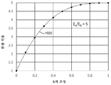
수학식 6을 사용하여, "편향 비율"또는 상대적 편향의 양이 도 10에 평탄화 재료의 높이(b)(즉, 도 10의 "b의 조성")의 함수로서 도 10의 그래프(플롯(1020))에 플롯화된다. 이 플롯으로부터, 평탄화 재료가 피쳐에 통합되지 않을 때, 즉 피쳐가 전체적으로 SOC 재료로 구성되는 경우, 상대적 편향은 1의 그 최소치라는 것을 알 수 있다. SOC 재료가 적용되지 않는 경우, 즉 피쳐가 전체적으로 평탄화 재료로 구성되는 경우, 이때, 편향은 5의 인자만큼 점프하고, 전술한 바와 같이, 그 자체로 사용될 때 평탄화 재료의 낮은 기계적 강성도로 인해, 2.5:1보다 양호한 종횡비를 지지할 수 없다.Using
그러나 여기에서 중요한 점은 다층 스택의 저부 층으로서 작은 양의 평탄화 재료를 통합해도 피쳐 압궤가 발생하는 상황이 발생한다는 것이다. 예로서, 다시 도 10을 참조하면, 전체 피쳐 두께의 10 %만이 평탄화 재료인 경우 편향 비율은 전체적으로 SOC를 사용하는 것에 비해 2배(2X)가 된다. 이런 편향 비율의 증가는 유효 모듈러스가 2의 인자만큼 감소함을 의미한다. SOC 영 모듈러스 원래 5GPa이고 평탄화 막이 1의 모듈러스를 갖는 경우, 그후, 평탄화 막의 10 % 만 저부 층으로서 추가함으로써, 유효 영 모듈러스는 단지 2.5로 떨어지며, 이는 도 4의 플롯(402)에 따라, 4:1보다 큰 종횡비를 유지하기에 불충분하다.However, what is important here is that even when a small amount of planarizing material is incorporated as the bottom layer of the multilayer stack, a situation occurs in which feature collapse occurs. By way of example, referring again to FIG. 10, if only 10% of the total feature thickness is a planarizing material, the deflection ratio is 2X (2X) compared to using SOC as a whole. This increase in deflection ratio means that the effective modulus is reduced by a factor of two. SOC < / RTI > Young Modulus Originally 5 GPa and the planarizing film had a modulus of 1, then by adding only 10% of the planarizing film as a bottom layer, the effective Young's modulus dropped to only 2.5, Is insufficient to maintain an aspect ratio greater than one.
제2 예로서, 표적 종횡비가 4:1 바로 아래로 완화되는 경우, 이때, 저부 층으로서 10 % 평탄화 막을 갖는 복합재 스택은 4:1 미만의 종횡비를 지지하기 위한 기계적 강성도 요건을 충족시키도록 작동할 수 있다. 그러나, 예로서 15nm의 기존 토포그래피가 존재하고 30nm 임계 피쳐 크기가 필요한 경우, 이때, 복합재 막의 높이는 120nm가 된다. 따라서, 10 % 평탄화 막은 단지 12nm의 두께를 가지며, 이는 평탄화 막이 기존의 15nm의 토포그래피 변화를 평탄하게 하기 위해 충분한 평탄화 막이 피착되지 않을 것이라는 것을 의미한다. 결과적으로, 종횡비가 낮은 완화된 경우에도, 후속 에칭에 필요한 종횡비 그리고 또한 하부 토포그래피 문제를 해결하기에 충분한 두께의 평탄화 막 모두를 해결하는 복합재 막 스택이 제공될 수 없다. 증가된 토포그래피 변화가 도입됨에 따라, 보다 두꺼운 평탄화 막의 필요성이 생성될 때, 평탄화 층이 먼저 피착되는 경우의 연장으로서, 심지어 4:1보다 낮은 다수의 종횡비가 지지될 수 없다.As a second example, if the target aspect ratio is relaxed to just below 4: 1, then the composite stack with the 10% planarizing film as the bottom layer will operate to meet the mechanical stiffness requirements to support an aspect ratio of less than 4: 1 . However, if for example an existing topography of 15 nm is present and a 30 nm critical feature size is required, then the height of the composite film will be 120 nm. Thus, the 10% planarizing film has a thickness of only 12 nm, which means that the planarizing film will not have a sufficient planarizing film deposited to flatten the existing 15 nm topography change. As a result, even if the aspect ratio is relaxed, a composite film stack can not be provided that solves both the aspect ratio required for subsequent etching and also the planarization film, which is sufficient to solve the underlying topography problem. As increased topography variations are introduced, multiple aspect ratios lower than 4: 1 can not be sustained as an extension of the planarization layer being deposited first, as the need for thicker planarization films is created.
다양한 양태들의 추가의 수정 및 대안적인 실시예는 이 설명을 고려하여 통상의 숙련자에게 명백할 것이다. 따라서, 이 설명은 단지 예시적인 것으로 해석되어야 한다. 본 명세서에 도시되고 설명된 형태는 실시예의 예로서 취해진 것으로 이해된다. 본 명세서에 도시되고 기술된 것들에 대해 요소들 및 재료들이 대체될 수 있으며, 이 설명의 이점을 얻은 후에 통상의 숙련자에게 명백한 바와 같이, 부품 및 프로세스들이 역전될 수 있고, 특정 특징들이 독립적으로 이용될 수 있다.Additional modifications and alternative embodiments of various aspects will be apparent to those of ordinary skill in the art in view of this description. Accordingly, this description is to be construed as illustrative only. It is to be understood that the form shown and described herein is taken as an example of an embodiment. Elements and materials may be substituted for those shown and described herein and, after obtaining the benefit of this description, as will be apparent to one of ordinary skill in the art, the parts and processes may be reversed and certain features may be utilized independently .
Claims (13)
상기 기판 위에 제1 기저층을 부착하는 단계로서, 형성되는 상기 제1 기저층이 아래에 있는 상기 기판의 비-평면 표면 변화에 대응하는 비평면 표면 변화를 갖는, 제1 기저층을 부착하는 단계, 및
상기 제1 기저층 위에 제2 평탄화층을 부착하는 단계
에 의해, 상기 기판 상에 다층 스택을 형성하는 단계;
상기 다층 스택 상에 하드 마스크를 피착하는 단계; 및
상기 하드 마스크 상에 패터닝된 층을 형성하는 단계를 포함하고,
형성된 상기 패터닝된 층은 피쳐(features)를 갖고,
상기 다층 스택은, 50nm 이하의 피쳐 치수 및 2.5:1 이상의 종횡비를 갖는 하나 이상의 에칭된 피쳐를 최소 피쳐 압궤(collapse)로 유지하는 데 충분한 복합 유효 기계적 강성도(Eeff)를 갖는, 방법.Providing a substrate having a surface with a non-planar surface change;
Attaching a first base layer on the substrate, the first base layer being formed having a non-planar surface change corresponding to a non-planar surface variation of the substrate underlying the first base layer; and
Attaching a second planarization layer on the first base layer
Forming a multilayer stack on the substrate;
Depositing a hard mask on the multilayer stack; And
Forming a patterned layer on the hard mask,
The patterned layer formed has features,
Wherein the multilayer stack has a composite effective mechanical stiffness (E eff ) sufficient to maintain at least one etched feature with a feature dimension of 50 nm or less and an aspect ratio of 2.5: 1 or more at a minimum feature collapse.
비-평면 표면 변화가 있는 표면을 갖는 기판;
상기 기판의 표면 위에 형성되고, 상기 기판 표면의 비-평면 표면 변화에 대응하는 비-평면 표면 변화를 갖는 제1 탄소 층; 및
상기 제1 탄소 층 위에 형성되고 평면 표면을 갖는 제2 평탄화 층을 포함하며,
다층 스택은 2.5:1 이상의 종횡비에서 50nm 이하의 피쳐를 최소 피쳐 압궤로 유지하는 데 충분한 복합 유효 기계적 강성도(Eeff)를 갖는, 다층 스택.Layer stack,
A substrate having a surface with a non-planar surface change;
A first carbon layer formed on a surface of the substrate and having a non-planar surface change corresponding to a non-planar surface variation of the substrate surface; And
A second planarization layer formed over the first carbon layer and having a planar surface,
The multilayer stack has a composite effective mechanical stiffness (E eff ) sufficient to maintain a feature of 50 nm or less at the minimum feature collapse at an aspect ratio of 2.5: 1 or more.
제8항의 방법에 따라 형성된 패터닝된 층의 피쳐를 기판으로 전사하는 단계, 및
상기 기판을 처리하여 디바이스를 제조하는 단계를 포함하는, 방법.A method of manufacturing a device,
Transferring the features of the patterned layer formed according to the method of claim 8 to a substrate, and
And processing the substrate to produce a device.
Applications Claiming Priority (2)
| Application Number | Priority Date | Filing Date | Title |
|---|---|---|---|
| US15/441,381 | 2017-02-24 | ||
| US15/441,381 US10079152B1 (en) | 2017-02-24 | 2017-02-24 | Method for forming planarized etch mask structures over existing topography |
Publications (2)
| Publication Number | Publication Date |
|---|---|
| KR20180098138A true KR20180098138A (en) | 2018-09-03 |
| KR102253295B1 KR102253295B1 (en) | 2021-05-20 |
Family
ID=63246983
Family Applications (1)
| Application Number | Title | Priority Date | Filing Date |
|---|---|---|---|
| KR1020180017407A KR102253295B1 (en) | 2017-02-24 | 2018-02-13 | Method for forming planarized etch mask structures over existing topography |
Country Status (3)
| Country | Link |
|---|---|
| US (1) | US10079152B1 (en) |
| JP (1) | JP7222606B2 (en) |
| KR (1) | KR102253295B1 (en) |
Families Citing this family (6)
| Publication number | Priority date | Publication date | Assignee | Title |
|---|---|---|---|---|
| JP7403961B2 (en) * | 2019-03-19 | 2023-12-25 | キオクシア株式会社 | Imprint method and semiconductor device manufacturing method |
| JP7336303B2 (en) * | 2019-07-31 | 2023-08-31 | キヤノン株式会社 | Article manufacturing method, film forming method, mold manufacturing method, article manufacturing system, information processing method and program |
| US11567401B2 (en) * | 2019-12-20 | 2023-01-31 | Canon Kabushiki Kaisha | Nanofabrication method with correction of distortion within an imprint system |
| US11656546B2 (en) | 2020-02-27 | 2023-05-23 | Canon Kabushiki Kaisha | Exposure apparatus for uniform light intensity and methods of using the same |
| US11349061B2 (en) * | 2020-06-08 | 2022-05-31 | International Business Machines Corporation | Glassy carbon mask for immersion implant and selective laser anneal |
| US11443940B2 (en) * | 2020-06-24 | 2022-09-13 | Canon Kabushiki Kaisha | Apparatus for uniform light intensity and methods of using the same |
Citations (4)
| Publication number | Priority date | Publication date | Assignee | Title |
|---|---|---|---|---|
| US20050184637A1 (en) * | 2004-01-29 | 2005-08-25 | Asahi Glass Company, Limited | Envelope for a flat panel display and flat panel display employing the envelope |
| US20130068720A1 (en) * | 2011-09-16 | 2013-03-21 | Shuichi Taniguchi | Pattern forming method |
| US20140227887A1 (en) * | 2011-09-06 | 2014-08-14 | Dongjin Semichem Co., Ltd. | Phenol-based self-crosslinking polymer and resist underlayer film composition including same |
| US20170003568A1 (en) * | 2014-01-30 | 2017-01-05 | Sony Corporation | Display unit and electronic apparatus |
Family Cites Families (15)
| Publication number | Priority date | Publication date | Assignee | Title |
|---|---|---|---|---|
| US6873087B1 (en) | 1999-10-29 | 2005-03-29 | Board Of Regents, The University Of Texas System | High precision orientation alignment and gap control stages for imprint lithography processes |
| US7077992B2 (en) | 2002-07-11 | 2006-07-18 | Molecular Imprints, Inc. | Step and repeat imprint lithography processes |
| US6932934B2 (en) | 2002-07-11 | 2005-08-23 | Molecular Imprints, Inc. | Formation of discontinuous films during an imprint lithography process |
| US7179396B2 (en) | 2003-03-25 | 2007-02-20 | Molecular Imprints, Inc. | Positive tone bi-layer imprint lithography method |
| US7396475B2 (en) | 2003-04-25 | 2008-07-08 | Molecular Imprints, Inc. | Method of forming stepped structures employing imprint lithography |
| US7157036B2 (en) | 2003-06-17 | 2007-01-02 | Molecular Imprints, Inc | Method to reduce adhesion between a conformable region and a pattern of a mold |
| US7790231B2 (en) | 2003-07-10 | 2010-09-07 | Brewer Science Inc. | Automated process and apparatus for planarization of topographical surfaces |
| US8076386B2 (en) | 2004-02-23 | 2011-12-13 | Molecular Imprints, Inc. | Materials for imprint lithography |
| US7998651B2 (en) | 2006-05-15 | 2011-08-16 | Asml Netherlands B.V. | Imprint lithography |
| US11392037B2 (en) * | 2008-02-18 | 2022-07-19 | Nissan Chemical Industries, Ltd. | Resist underlayer film forming composition containing silicone having cyclic amino group |
| US8071275B2 (en) | 2008-04-10 | 2011-12-06 | Lexmark International, Inc. | Methods for planarizing unevenness on surface of wafer photoresist layer and wafers produced by the methods |
| CN102089708A (en) | 2008-06-09 | 2011-06-08 | 得克萨斯州大学系统董事会 | Adaptive nanotopography sculpting |
| WO2013109748A1 (en) * | 2012-01-19 | 2013-07-25 | Brewer Science Inc. | Nonpolymeric antireflection compositions containing adamantyl groups |
| SG11201601162TA (en) | 2013-08-19 | 2016-03-30 | Univ Texas | Programmable deposition of thin films of a user-defined profile with nanometer scale accuracy |
| KR102351281B1 (en) * | 2013-09-11 | 2022-01-14 | 제이에스알 가부시끼가이샤 | Composition for forming inorganic film for multilayer resist process, and pattern formation method |
-
2017
- 2017-02-24 US US15/441,381 patent/US10079152B1/en active Active
-
2018
- 2018-02-13 KR KR1020180017407A patent/KR102253295B1/en active IP Right Grant
- 2018-02-19 JP JP2018027233A patent/JP7222606B2/en active Active
Patent Citations (5)
| Publication number | Priority date | Publication date | Assignee | Title |
|---|---|---|---|---|
| US20050184637A1 (en) * | 2004-01-29 | 2005-08-25 | Asahi Glass Company, Limited | Envelope for a flat panel display and flat panel display employing the envelope |
| US20140227887A1 (en) * | 2011-09-06 | 2014-08-14 | Dongjin Semichem Co., Ltd. | Phenol-based self-crosslinking polymer and resist underlayer film composition including same |
| US20130068720A1 (en) * | 2011-09-16 | 2013-03-21 | Shuichi Taniguchi | Pattern forming method |
| JP2013065725A (en) * | 2011-09-16 | 2013-04-11 | Toshiba Corp | Pattern formation method |
| US20170003568A1 (en) * | 2014-01-30 | 2017-01-05 | Sony Corporation | Display unit and electronic apparatus |
Also Published As
| Publication number | Publication date |
|---|---|
| US20180247823A1 (en) | 2018-08-30 |
| US10079152B1 (en) | 2018-09-18 |
| JP7222606B2 (en) | 2023-02-15 |
| KR102253295B1 (en) | 2021-05-20 |
| JP2018142701A (en) | 2018-09-13 |
Similar Documents
| Publication | Publication Date | Title |
|---|---|---|
| KR102253295B1 (en) | Method for forming planarized etch mask structures over existing topography | |
| US8012394B2 (en) | Template pattern density doubling | |
| US7960090B2 (en) | Pattern forming method, pattern formed thereby, mold, processing apparatus, and processing method | |
| US8961852B2 (en) | Templates having high contrast alignment marks | |
| US7357876B2 (en) | Eliminating printability of sub-resolution defects in imprint lithography | |
| US7140861B2 (en) | Compliant hard template for UV imprinting | |
| US10211051B2 (en) | Method of reverse tone patterning | |
| JP5404654B2 (en) | Limit dimension control during template formation | |
| US20200225575A1 (en) | Apparatus for Separating a Master Template from a Replica Template | |
| JP2009182075A (en) | Manufacturing method of structure by imprint | |
| KR102379626B1 (en) | Nanoimprint template with light blocking material and method of fabrication | |
| US7985530B2 (en) | Etch-enhanced technique for lift-off patterning | |
| JP5848386B2 (en) | In-situ insertion structure forming method | |
| JP2013503057A (en) | Functional nanoparticles | |
| US8935981B2 (en) | High contrast alignment marks through multiple stage imprinting | |
| US20100095862A1 (en) | Double Sidewall Angle Nano-Imprint Template | |
| KR20210080218A (en) | Nanofabrication method with correction of distortion whithin an imprint system | |
| US20230205080A1 (en) | Template, method of forming a template, apparatus and method of manufacturing an article | |
| JP2018160537A (en) | Pattern forming method | |
| TW202400507A (en) | Methods for fabricating imprint lithography templates, optical components and diffractive optical elements | |
| KR20220034874A (en) | Methods for planarization of spin-on and CVD deposited organic films |
Legal Events
| Date | Code | Title | Description |
|---|---|---|---|
| A201 | Request for examination | ||
| E902 | Notification of reason for refusal | ||
| E701 | Decision to grant or registration of patent right | ||
| GRNT | Written decision to grant |