KR20170099018A - Memory system and operation method for the same - Google Patents
Memory system and operation method for the same Download PDFInfo
- Publication number
- KR20170099018A KR20170099018A KR1020160020551A KR20160020551A KR20170099018A KR 20170099018 A KR20170099018 A KR 20170099018A KR 1020160020551 A KR1020160020551 A KR 1020160020551A KR 20160020551 A KR20160020551 A KR 20160020551A KR 20170099018 A KR20170099018 A KR 20170099018A
- Authority
- KR
- South Korea
- Prior art keywords
- bit information
- memory
- error bit
- memory blocks
- garbage collection
- Prior art date
Links
Images


Classifications
-
- G—PHYSICS
- G06—COMPUTING; CALCULATING OR COUNTING
- G06F—ELECTRIC DIGITAL DATA PROCESSING
- G06F12/00—Accessing, addressing or allocating within memory systems or architectures
- G06F12/02—Addressing or allocation; Relocation
- G06F12/0223—User address space allocation, e.g. contiguous or non contiguous base addressing
- G06F12/023—Free address space management
- G06F12/0238—Memory management in non-volatile memory, e.g. resistive RAM or ferroelectric memory
- G06F12/0246—Memory management in non-volatile memory, e.g. resistive RAM or ferroelectric memory in block erasable memory, e.g. flash memory
-
- G—PHYSICS
- G06—COMPUTING; CALCULATING OR COUNTING
- G06F—ELECTRIC DIGITAL DATA PROCESSING
- G06F3/00—Input arrangements for transferring data to be processed into a form capable of being handled by the computer; Output arrangements for transferring data from processing unit to output unit, e.g. interface arrangements
- G06F3/06—Digital input from, or digital output to, record carriers, e.g. RAID, emulated record carriers or networked record carriers
- G06F3/0601—Interfaces specially adapted for storage systems
- G06F3/0602—Interfaces specially adapted for storage systems specifically adapted to achieve a particular effect
- G06F3/0614—Improving the reliability of storage systems
-
- G—PHYSICS
- G06—COMPUTING; CALCULATING OR COUNTING
- G06F—ELECTRIC DIGITAL DATA PROCESSING
- G06F12/00—Accessing, addressing or allocating within memory systems or architectures
- G06F12/02—Addressing or allocation; Relocation
- G06F12/0223—User address space allocation, e.g. contiguous or non contiguous base addressing
- G06F12/023—Free address space management
- G06F12/0253—Garbage collection, i.e. reclamation of unreferenced memory
-
- G—PHYSICS
- G06—COMPUTING; CALCULATING OR COUNTING
- G06F—ELECTRIC DIGITAL DATA PROCESSING
- G06F11/00—Error detection; Error correction; Monitoring
- G06F11/07—Responding to the occurrence of a fault, e.g. fault tolerance
- G06F11/08—Error detection or correction by redundancy in data representation, e.g. by using checking codes
- G06F11/10—Adding special bits or symbols to the coded information, e.g. parity check, casting out 9's or 11's
- G06F11/1008—Adding special bits or symbols to the coded information, e.g. parity check, casting out 9's or 11's in individual solid state devices
- G06F11/1012—Adding special bits or symbols to the coded information, e.g. parity check, casting out 9's or 11's in individual solid state devices using codes or arrangements adapted for a specific type of error
-
- G—PHYSICS
- G06—COMPUTING; CALCULATING OR COUNTING
- G06F—ELECTRIC DIGITAL DATA PROCESSING
- G06F11/00—Error detection; Error correction; Monitoring
- G06F11/07—Responding to the occurrence of a fault, e.g. fault tolerance
- G06F11/08—Error detection or correction by redundancy in data representation, e.g. by using checking codes
- G06F11/10—Adding special bits or symbols to the coded information, e.g. parity check, casting out 9's or 11's
- G06F11/1008—Adding special bits or symbols to the coded information, e.g. parity check, casting out 9's or 11's in individual solid state devices
- G06F11/1048—Adding special bits or symbols to the coded information, e.g. parity check, casting out 9's or 11's in individual solid state devices using arrangements adapted for a specific error detection or correction feature
-
- G—PHYSICS
- G06—COMPUTING; CALCULATING OR COUNTING
- G06F—ELECTRIC DIGITAL DATA PROCESSING
- G06F11/00—Error detection; Error correction; Monitoring
- G06F11/07—Responding to the occurrence of a fault, e.g. fault tolerance
- G06F11/08—Error detection or correction by redundancy in data representation, e.g. by using checking codes
- G06F11/10—Adding special bits or symbols to the coded information, e.g. parity check, casting out 9's or 11's
- G06F11/1008—Adding special bits or symbols to the coded information, e.g. parity check, casting out 9's or 11's in individual solid state devices
- G06F11/1068—Adding special bits or symbols to the coded information, e.g. parity check, casting out 9's or 11's in individual solid state devices in sector programmable memories, e.g. flash disk
-
- G—PHYSICS
- G06—COMPUTING; CALCULATING OR COUNTING
- G06F—ELECTRIC DIGITAL DATA PROCESSING
- G06F11/00—Error detection; Error correction; Monitoring
- G06F11/07—Responding to the occurrence of a fault, e.g. fault tolerance
- G06F11/16—Error detection or correction of the data by redundancy in hardware
- G06F11/1666—Error detection or correction of the data by redundancy in hardware where the redundant component is memory or memory area
-
- G—PHYSICS
- G06—COMPUTING; CALCULATING OR COUNTING
- G06F—ELECTRIC DIGITAL DATA PROCESSING
- G06F13/00—Interconnection of, or transfer of information or other signals between, memories, input/output devices or central processing units
- G06F13/14—Handling requests for interconnection or transfer
- G06F13/16—Handling requests for interconnection or transfer for access to memory bus
- G06F13/1668—Details of memory controller
-
- G—PHYSICS
- G06—COMPUTING; CALCULATING OR COUNTING
- G06F—ELECTRIC DIGITAL DATA PROCESSING
- G06F3/00—Input arrangements for transferring data to be processed into a form capable of being handled by the computer; Output arrangements for transferring data from processing unit to output unit, e.g. interface arrangements
- G06F3/06—Digital input from, or digital output to, record carriers, e.g. RAID, emulated record carriers or networked record carriers
- G06F3/0601—Interfaces specially adapted for storage systems
- G06F3/0602—Interfaces specially adapted for storage systems specifically adapted to achieve a particular effect
- G06F3/061—Improving I/O performance
-
- G—PHYSICS
- G06—COMPUTING; CALCULATING OR COUNTING
- G06F—ELECTRIC DIGITAL DATA PROCESSING
- G06F3/00—Input arrangements for transferring data to be processed into a form capable of being handled by the computer; Output arrangements for transferring data from processing unit to output unit, e.g. interface arrangements
- G06F3/06—Digital input from, or digital output to, record carriers, e.g. RAID, emulated record carriers or networked record carriers
- G06F3/0601—Interfaces specially adapted for storage systems
- G06F3/0628—Interfaces specially adapted for storage systems making use of a particular technique
- G06F3/0638—Organizing or formatting or addressing of data
- G06F3/064—Management of blocks
-
- G—PHYSICS
- G06—COMPUTING; CALCULATING OR COUNTING
- G06F—ELECTRIC DIGITAL DATA PROCESSING
- G06F3/00—Input arrangements for transferring data to be processed into a form capable of being handled by the computer; Output arrangements for transferring data from processing unit to output unit, e.g. interface arrangements
- G06F3/06—Digital input from, or digital output to, record carriers, e.g. RAID, emulated record carriers or networked record carriers
- G06F3/0601—Interfaces specially adapted for storage systems
- G06F3/0628—Interfaces specially adapted for storage systems making use of a particular technique
- G06F3/0646—Horizontal data movement in storage systems, i.e. moving data in between storage devices or systems
- G06F3/0652—Erasing, e.g. deleting, data cleaning, moving of data to a wastebasket
-
- G—PHYSICS
- G06—COMPUTING; CALCULATING OR COUNTING
- G06F—ELECTRIC DIGITAL DATA PROCESSING
- G06F3/00—Input arrangements for transferring data to be processed into a form capable of being handled by the computer; Output arrangements for transferring data from processing unit to output unit, e.g. interface arrangements
- G06F3/06—Digital input from, or digital output to, record carriers, e.g. RAID, emulated record carriers or networked record carriers
- G06F3/0601—Interfaces specially adapted for storage systems
- G06F3/0628—Interfaces specially adapted for storage systems making use of a particular technique
- G06F3/0662—Virtualisation aspects
- G06F3/0665—Virtualisation aspects at area level, e.g. provisioning of virtual or logical volumes
-
- G—PHYSICS
- G06—COMPUTING; CALCULATING OR COUNTING
- G06F—ELECTRIC DIGITAL DATA PROCESSING
- G06F3/00—Input arrangements for transferring data to be processed into a form capable of being handled by the computer; Output arrangements for transferring data from processing unit to output unit, e.g. interface arrangements
- G06F3/06—Digital input from, or digital output to, record carriers, e.g. RAID, emulated record carriers or networked record carriers
- G06F3/0601—Interfaces specially adapted for storage systems
- G06F3/0668—Interfaces specially adapted for storage systems adopting a particular infrastructure
- G06F3/0671—In-line storage system
- G06F3/0673—Single storage device
- G06F3/0679—Non-volatile semiconductor memory device, e.g. flash memory, one time programmable memory [OTP]
-
- G—PHYSICS
- G11—INFORMATION STORAGE
- G11C—STATIC STORES
- G11C29/00—Checking stores for correct operation ; Subsequent repair; Testing stores during standby or offline operation
- G11C29/02—Detection or location of defective auxiliary circuits, e.g. defective refresh counters
- G11C29/022—Detection or location of defective auxiliary circuits, e.g. defective refresh counters in I/O circuitry
-
- G—PHYSICS
- G11—INFORMATION STORAGE
- G11C—STATIC STORES
- G11C7/00—Arrangements for writing information into, or reading information out from, a digital store
- G11C7/10—Input/output [I/O] data interface arrangements, e.g. I/O data control circuits, I/O data buffers
-
- G—PHYSICS
- G06—COMPUTING; CALCULATING OR COUNTING
- G06F—ELECTRIC DIGITAL DATA PROCESSING
- G06F2212/00—Indexing scheme relating to accessing, addressing or allocation within memory systems or architectures
- G06F2212/10—Providing a specific technical effect
- G06F2212/1016—Performance improvement
-
- G—PHYSICS
- G06—COMPUTING; CALCULATING OR COUNTING
- G06F—ELECTRIC DIGITAL DATA PROCESSING
- G06F2212/00—Indexing scheme relating to accessing, addressing or allocation within memory systems or architectures
- G06F2212/72—Details relating to flash memory management
- G06F2212/7205—Cleaning, compaction, garbage collection, erase control
-
- G—PHYSICS
- G11—INFORMATION STORAGE
- G11C—STATIC STORES
- G11C29/00—Checking stores for correct operation ; Subsequent repair; Testing stores during standby or offline operation
- G11C29/04—Detection or location of defective memory elements, e.g. cell constructio details, timing of test signals
- G11C29/08—Functional testing, e.g. testing during refresh, power-on self testing [POST] or distributed testing
- G11C29/12—Built-in arrangements for testing, e.g. built-in self testing [BIST] or interconnection details
- G11C29/44—Indication or identification of errors, e.g. for repair
- G11C29/4401—Indication or identification of errors, e.g. for repair for self repair
-
- G—PHYSICS
- G11—INFORMATION STORAGE
- G11C—STATIC STORES
- G11C29/00—Checking stores for correct operation ; Subsequent repair; Testing stores during standby or offline operation
- G11C29/52—Protection of memory contents; Detection of errors in memory contents
-
- H—ELECTRICITY
- H03—ELECTRONIC CIRCUITRY
- H03M—CODING; DECODING; CODE CONVERSION IN GENERAL
- H03M13/00—Coding, decoding or code conversion, for error detection or error correction; Coding theory basic assumptions; Coding bounds; Error probability evaluation methods; Channel models; Simulation or testing of codes
- H03M13/03—Error detection or forward error correction by redundancy in data representation, i.e. code words containing more digits than the source words
- H03M13/05—Error detection or forward error correction by redundancy in data representation, i.e. code words containing more digits than the source words using block codes, i.e. a predetermined number of check bits joined to a predetermined number of information bits
- H03M13/11—Error detection or forward error correction by redundancy in data representation, i.e. code words containing more digits than the source words using block codes, i.e. a predetermined number of check bits joined to a predetermined number of information bits using multiple parity bits
- H03M13/1102—Codes on graphs and decoding on graphs, e.g. low-density parity check [LDPC] codes
-
- H—ELECTRICITY
- H03—ELECTRONIC CIRCUITRY
- H03M—CODING; DECODING; CODE CONVERSION IN GENERAL
- H03M13/00—Coding, decoding or code conversion, for error detection or error correction; Coding theory basic assumptions; Coding bounds; Error probability evaluation methods; Channel models; Simulation or testing of codes
- H03M13/03—Error detection or forward error correction by redundancy in data representation, i.e. code words containing more digits than the source words
- H03M13/05—Error detection or forward error correction by redundancy in data representation, i.e. code words containing more digits than the source words using block codes, i.e. a predetermined number of check bits joined to a predetermined number of information bits
- H03M13/13—Linear codes
- H03M13/15—Cyclic codes, i.e. cyclic shifts of codewords produce other codewords, e.g. codes defined by a generator polynomial, Bose-Chaudhuri-Hocquenghem [BCH] codes
- H03M13/151—Cyclic codes, i.e. cyclic shifts of codewords produce other codewords, e.g. codes defined by a generator polynomial, Bose-Chaudhuri-Hocquenghem [BCH] codes using error location or error correction polynomials
- H03M13/1515—Reed-Solomon codes
-
- H—ELECTRICITY
- H03—ELECTRONIC CIRCUITRY
- H03M—CODING; DECODING; CODE CONVERSION IN GENERAL
- H03M13/00—Coding, decoding or code conversion, for error detection or error correction; Coding theory basic assumptions; Coding bounds; Error probability evaluation methods; Channel models; Simulation or testing of codes
- H03M13/03—Error detection or forward error correction by redundancy in data representation, i.e. code words containing more digits than the source words
- H03M13/05—Error detection or forward error correction by redundancy in data representation, i.e. code words containing more digits than the source words using block codes, i.e. a predetermined number of check bits joined to a predetermined number of information bits
- H03M13/13—Linear codes
- H03M13/15—Cyclic codes, i.e. cyclic shifts of codewords produce other codewords, e.g. codes defined by a generator polynomial, Bose-Chaudhuri-Hocquenghem [BCH] codes
- H03M13/151—Cyclic codes, i.e. cyclic shifts of codewords produce other codewords, e.g. codes defined by a generator polynomial, Bose-Chaudhuri-Hocquenghem [BCH] codes using error location or error correction polynomials
- H03M13/152—Bose-Chaudhuri-Hocquenghem [BCH] codes
-
- H—ELECTRICITY
- H03—ELECTRONIC CIRCUITRY
- H03M—CODING; DECODING; CODE CONVERSION IN GENERAL
- H03M13/00—Coding, decoding or code conversion, for error detection or error correction; Coding theory basic assumptions; Coding bounds; Error probability evaluation methods; Channel models; Simulation or testing of codes
- H03M13/03—Error detection or forward error correction by redundancy in data representation, i.e. code words containing more digits than the source words
- H03M13/05—Error detection or forward error correction by redundancy in data representation, i.e. code words containing more digits than the source words using block codes, i.e. a predetermined number of check bits joined to a predetermined number of information bits
- H03M13/13—Linear codes
- H03M13/19—Single error correction without using particular properties of the cyclic codes, e.g. Hamming codes, extended or generalised Hamming codes
-
- H—ELECTRICITY
- H03—ELECTRONIC CIRCUITRY
- H03M—CODING; DECODING; CODE CONVERSION IN GENERAL
- H03M13/00—Coding, decoding or code conversion, for error detection or error correction; Coding theory basic assumptions; Coding bounds; Error probability evaluation methods; Channel models; Simulation or testing of codes
- H03M13/03—Error detection or forward error correction by redundancy in data representation, i.e. code words containing more digits than the source words
- H03M13/23—Error detection or forward error correction by redundancy in data representation, i.e. code words containing more digits than the source words using convolutional codes, e.g. unit memory codes
-
- H—ELECTRICITY
- H03—ELECTRONIC CIRCUITRY
- H03M—CODING; DECODING; CODE CONVERSION IN GENERAL
- H03M13/00—Coding, decoding or code conversion, for error detection or error correction; Coding theory basic assumptions; Coding bounds; Error probability evaluation methods; Channel models; Simulation or testing of codes
- H03M13/29—Coding, decoding or code conversion, for error detection or error correction; Coding theory basic assumptions; Coding bounds; Error probability evaluation methods; Channel models; Simulation or testing of codes combining two or more codes or code structures, e.g. product codes, generalised product codes, concatenated codes, inner and outer codes
- H03M13/2957—Turbo codes and decoding
Landscapes
- Engineering & Computer Science (AREA)
- Theoretical Computer Science (AREA)
- Physics & Mathematics (AREA)
- General Engineering & Computer Science (AREA)
- General Physics & Mathematics (AREA)
- Human Computer Interaction (AREA)
- Quality & Reliability (AREA)
- Read Only Memory (AREA)
- Semiconductor Memories (AREA)
- Probability & Statistics with Applications (AREA)
- Non-Volatile Memory (AREA)
Abstract
Description
본 발명은 메모리 시스템의 가비지 컬렉션 동작에 관한 것으로서, 더욱 상세하게는 에러 비트 정보를 바탕으로 가비지 컬렉션 동작을 수행하는 메모리 시스템 및 그 동작방법에 관한 것이다.BACKGROUND OF THE
최근 컴퓨터 환경에 대한 패러다임(paradigm)이 언제, 어디서나 컴퓨터 시스템을 사용할 수 있도록 하는 유비쿼터스 컴퓨팅(ubiquitous computing)으로 전환되고 있다. 이로 인해 휴대폰, 디지털 카메라, 노트북 컴퓨터 등과 같은 휴대용 전자 장치의 사용이 급증하고 있다. 이와 같은 휴대용 전자 장치는 일반적으로 메모리 장치를 이용하는 메모리 시스템, 다시 말해 데이터 저장 장치를 사용한다. 데이터 저장 장치는 휴대용 전자 장치의 주 기억 장치 또는 보조 기억 장치로 사용된다. Recently, a paradigm for a computer environment has been transformed into ubiquitous computing, which enables a computer system to be used whenever and wherever. As a result, the use of portable electronic devices such as mobile phones, digital cameras, and notebook computers is rapidly increasing. Such portable electronic devices typically use memory systems that use memory devices, i. E., Data storage devices. The data storage device is used as a main storage device or an auxiliary storage device of a portable electronic device.
메모리 장치를 이용한 데이터 저장 장치는 기계적인 구동부가 없어서 안정성 및 내구성이 뛰어나며, 또한 정보의 액세스 속도가 매우 빠르고 전력 소모가 적다는 장점이 있다. 이러한 장점을 갖는 데이터 저장 장치의 일 예로, USB(Universal Serial Bus) 메모리 장치, 다양한 인터페이스를 갖는 메모리 카드, 솔리드 스테이트 드라이브(SSD: Solid State Drive) 등이 포함된다.The data storage device using the memory device is advantageous in that it has excellent stability and durability because there is no mechanical driving part, and the access speed of information is very fast and power consumption is low. Examples of the data storage device having such advantages include a USB (Universal Serial Bus) memory device, a memory card having various interfaces, and a solid state drive (SSD).
본 발명은 에러 비트 정보를 바탕으로 가비지 컬렉션 동작을 수행하는 메모리 시스템 및 그 동작방법을 제공하고자 한다.The present invention provides a memory system and an operation method thereof for performing a garbage collection operation based on error bit information.
본 발명의 실시예에 따른 메모리 시스템은 다수의 메모리 블록들을 포함하는 메모리 장치; 및 상기 다수의 메모리 블록들 중에서 유효 페이지 수가 제1 임계값 이하인 제1 메모리 블록들에 대해 가비지 컬렉션 동작을 수행하는 컨트롤러를 포함할 수 있고, 상기 컨트롤러는 상기 제1 메모리 블록들에 대해 각각의 에러 비트 정보를 바탕으로 가비지 컬렉션 동작을 수행할 수 있다. A memory system according to an embodiment of the present invention includes a memory device including a plurality of memory blocks; And a controller for performing a garbage collection operation on the first memory blocks having the number of valid pages equal to or less than a first threshold value among the plurality of memory blocks, The garbage collection operation can be performed based on the bit information.
본 발명의 또 다른 실시예에 따른 메모리 시스템의 동작방법은, 각각 다수의 페이지들을 포함하는 복수의 메모리 블록들 중에서 유효 페이지 수가 제1 임계값 이하인 제1 메모리 블록들을 선택하는 단계; 및 상기 제1 메모리 블록들에 대해 각각의 에러 비트 정보를 바탕으로 가비지 컬렉션 동작을 수행하는 단계를 포함할 수 있다.According to still another aspect of the present invention, there is provided a method of operating a memory system, the method comprising: selecting first memory blocks having a number of valid pages equal to or less than a first threshold value among a plurality of memory blocks each including a plurality of pages; And performing a garbage collection operation on the first memory blocks based on the respective error bit information.
본 기술은 메모리 장치에서 무효 데이터들을 정리하여 저장 공간을 확보할 때, 특성이 취약해진 공간을 우선적으로 선별하여 정리할 수 있다. 따라서, 메모리 장치의 저장 공간을 확보함과 동시에, 프로그램/리드 동작 등에 발생할 수 있는 에러를 방지할 수 있다.When the storage space is secured by arranging the invalid data in the memory device, the technology can sort and sort the space with the weak characteristic. Therefore, it is possible to secure a storage space of the memory device and to prevent an error that may occur in the program / read operation and the like.
이를 위해, 리드 동작 시에 검출되는 에러 비트 정보를 관리함으로써 메모리 장치를 제어하는 컨트롤러의 오버헤드(overhead)를 줄이고, 메모리 장치의 동작 속도 또한 증가시킬 수 있다. To this end, by managing the error bit information detected during the read operation, it is possible to reduce the overhead of the controller for controlling the memory device and increase the operation speed of the memory device.
도 1은 본 발명의 실시예에 따른 메모리 시스템을 포함하는 데이터 처리 시스템을 개략적으로 도시한 도면.
도 2는 본 발명의 실시예에 따른 메모리 시스템에서 메모리 장치를 개략적으로 도시한 도면.
도 3은 본 발명의 실시예에 따른 메모리 장치에서 메모리 블록들의 메모리 셀 어레이 회로를 개략적으로 도시한 도면.
도 4 내지 도 11은 본 발명의 실시예에 따른 메모리 시스템에서 메모리 장치 구조를 개략적으로 도시한 도면.
도 12는 본 발명의 실시예에 따른 메모리 시스템을 개략적으로 도시한 도면.
도 13은 도 12의 메모리 장치의 에러 비트 정보를 검출하는 동작을 설명하기 위한 도면.
도 14는 본 발명의 실시예에 따른 가비지 컬렉션 정보와 최대 에러 비트 정보를 저장하는 관리 테이블을 도시한 도면.
도 15는 본 발명의 실시예에 따른 도 12의 메모리 시스템의 전반적인 동작을 설명하기 위한 도면.1 schematically depicts a data processing system including a memory system according to an embodiment of the invention;
Figure 2 schematically illustrates a memory device in a memory system according to an embodiment of the present invention;
3 schematically shows a memory cell array circuit of memory blocks in a memory device according to an embodiment of the present invention.
Figures 4-11 schematically illustrate a memory device structure in a memory system according to an embodiment of the present invention.
12 schematically illustrates a memory system in accordance with an embodiment of the present invention.
13 is a view for explaining an operation of detecting error bit information in the memory device of Fig. 12; Fig.
FIG. 14 illustrates a management table storing garbage collection information and maximum error bit information according to an embodiment of the present invention; FIG.
FIG. 15 is a diagram for explaining an overall operation of the memory system of FIG. 12 according to the embodiment of the present invention; FIG.
이하, 본 발명이 속하는 기술 분야에서 통상의 지식을 가진 자가 본 발명의 기술적 사상을 용이하게 실시할 수 있을 정도로 상세히 설명하기 위하여, 본 발명의 가장 바람직한 실시예를 첨부 도면을 참조하여 설명하기로 한다. 그러나, 본 발명은 이하에서 개시되는 실시예에 한정되는 것이 아니라 서로 다른 다양한 형태로 구성될 수 있으며, 단지 본 실시예는 본 발명의 개시가 완전하도록 하며 통상의 지식을 가진자에게 본 발명의 범주를 완전하게 알려주기 위해 제공되는 것이다.DETAILED DESCRIPTION OF THE PREFERRED EMBODIMENTS Hereinafter, preferred embodiments of the present invention will be described in detail with reference to the accompanying drawings in order to facilitate a person skilled in the art to easily carry out the technical idea of the present invention. . However, it is to be understood that the present invention is not limited to the disclosed embodiments, but may be embodied in many different forms and should not be construed as limited to the embodiments set forth herein, Is provided to fully inform the user.
도 1은 본 발명의 실시 예에 따른 메모리 시스템을 포함하는 데이터 처리 시스템의 일 예를 개략적으로 도시한 도면이다.1 is a diagram schematically illustrating an example of a data processing system including a memory system according to an embodiment of the present invention.
도 1을 참조하면, 데이터 처리 시스템(100)은, 호스트(Host)(102) 및 메모리 시스템(110)을 포함한다.Referring to FIG. 1, a
그리고, 호스트(102)는, 예컨대, 휴대폰, MP3 플레이어, 랩탑 컴퓨터 등과 같은 휴대용 전자 장치들, 또는 데스크탑 컴퓨터, 게임기, TV, 프로젝터 등과 같은 전자 장치들을 포함한다.The
또한, 메모리 시스템(110)은, 호스트(102)의 요청에 응답하여 동작하며, 특히 호스트(102)에 의해서 액세스되는 데이터를 저장한다. 다시 말해, 메모리 시스템(110)은, 호스트(102)의 주 기억 장치 또는 보조 기억 장치로 사용될 수 있다. 여기서, 메모리 시스템(110)은 호스트(102)와 연결되는 호스트 인터페이스 프로토콜에 따라, 다양한 종류의 저장 장치들 중 어느 하나로 구현될 수 있다. 예를 들면, 메모리 시스템(110)은, 솔리드 스테이트 드라이브(SSD: Solid State Drive), MMC, eMMC(embedded MMC), RS-MMC(Reduced Size MMC), micro-MMC 형태의 멀티 미디어 카드(MMC: Multi Media Card), SD, mini-SD, micro-SD 형태의 시큐어 디지털(SD: Secure Digital) 카드, USB(Universal Storage Bus) 저장 장치, UFS(Universal Flash Storage) 장치, CF(Compact Flash) 카드, 스마트 미디어(Smart Media) 카드, 메모리 스틱(Memory Stick) 등과 같은 다양한 종류의 저장 장치들 중 어느 하나로 구현될 수 있다.The
아울러, 메모리 시스템(110)을 구현하는 저장 장치들은, DRAM(Dynamic Random Access Memory), SRAM(Static RAM) 등과 같은 휘발성 메모리 장치와 ROM(Read Only Memory), MROM(Mask ROM), PROM(Programmable ROM), EPROM(Erasable Programmable ROM), EEPROM(Electrically Erasable Programmable ROM), FRAM(Ferroelectric RAM), PRAM(Phase-change RAM), MRAM(Magnetoresistive RAM), RRAM(Resistive RAM), 플래시 메모리 등과 같은 비휘발성 메모리 장치로 구현될 수 있다.In addition, the storage devices implementing the
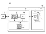
그리고, 메모리 시스템(110)은, 호스트(102)에 의해서 액세스되는 데이터를 저장하는 메모리 장치(150), 및 메모리 장치(150)로의 데이터 저장을 제어하는 컨트롤러(130)를 포함한다.The
여기서, 컨트롤러(130) 및 메모리 장치(150)는 하나의 반도체 장치로 집적될 수 있다. 일 예로, 컨트롤러(130) 및 메모리 장치(150)는 하나의 반도체 장치로 집적되어 SSD를 구성할 수 있다. 메모리 시스템(110)이 SSD로 이용되는 경우, 메모리 시스템(110)에 연결되는 호스트(102)의 동작 속도는 획기적으로 개선될 수 있다.Here, the
컨트롤러(130) 및 메모리 장치(150)는 하나의 반도체 장치로 집적되어, 메모리 카드를 구성할 수 있다. 예를 들면, 컨트롤러(130) 및 메모리 장치(150)는, 하나의 반도체 장치로 집적되어, PC 카드(PCMCIA: Personal Computer Memory Card International Association), 컴팩트 플래시 카드(CF), 스마트 미디어 카드(SM, SMC), 메모리 스틱, 멀티미디어 카드(MMC, RS-MMC, MMCmicro), SD 카드(SD, miniSD, microSD, SDHC), 유니버설 플래시 기억 장치(UFS) 등과 같은 메모리 카드를 구성할 수 있다.The
또 다른 일 예로, 메모리 시스템(110)은, 컴퓨터, UMPC (Ultra Mobile PC), 워크스테이션, 넷북(net-book), PDA (Personal Digital Assistant), 포터블(portable) 컴퓨터, 웹 태블릿(web tablet), 태블릿 컴퓨터(tablet computer), 무선 전화기(wireless phone), 모바일 폰(mobile phone), 스마트폰(smart phone), e-북(e-book), PMP(Portable Multimedia Player), 휴대용 게임기, 네비게이션(navigation) 장치, 블랙박스(black box), 디지털 카메라(digital camera), DMB (Digital Multimedia Broadcasting) 재생기, 3차원 텔레비전(3-dimensional television), 스마트 텔레비전(smart television), 디지털 음성 녹음기(digital audio recorder), 디지털 음성 재생기(digital audio player), 디지털 영상 녹화기(digital picture recorder), 디지털 영상 재생기(digital picture player), 디지털 동영상 녹화기(digital video recorder), 디지털 동영상 재생기(digital video player), 데이터 센터를 구성하는 스토리지, 정보를 무선 환경에서 송수신할 수 있는 장치, 홈 네트워크를 구성하는 다양한 전자 장치들 중 하나, 컴퓨터 네트워크를 구성하는 다양한 전자 장치들 중 하나, 텔레매틱스 네트워크를 구성하는 다양한 전자 장치들 중 하나, RFID 장치, 또는 컴퓨팅 시스템을 구성하는 다양한 구성 요소들 중 하나 등을 구성할 수 있다.In another example,
한편, 메모리 시스템(110)의 메모리 장치(150)는, 전원이 공급되지 않아도 저장된 데이터를 유지할 수 있으며, 특히 라이트(write) 동작을 통해 호스트(102)로부터 제공된 데이터를 저장하고, 리드(read) 동작을 통해 저장된 데이터를 호스트(102)로 제공한다. 그리고, 메모리 장치(150)는, 복수의 메모리 블록(memory block)들(152,154,156)을 포함하며, 각각의 메모리 블록들은, 복수의 페이지(page)들을 포함하며, 또한 각각의 페이지들은, 복수의 워드라인(WL: Word Line)들이 연결된 복수의 메모리 셀들을 포함한다. 또한, 메모리 장치(150)는, 비휘발성 메모리 장치, 일 예로 플래시 메모리가 될 수 있으며, 이때 플래시 메모리는 3D 입체 스택(stack) 구조가 될 수 있다. 여기서, 메모리 장치(150)의 구조 및 메모리 장치(150)의 3D 입체 스택 구조에 대해서는, 이하 도 2 내지 도 11을 참조하여 보다 구체적으로 설명할 예정임으로, 여기서는 그에 관한 구체적인 설명을 생략하기로 한다.Meanwhile, the
그리고, 메모리 시스템(110)의 컨트롤러(130)는, 호스트(102)로부터의 요청에 응답하여 메모리 장치(150)를 제어한다. 예컨대, 컨트롤러(130)는, 메모리 장치(150)로부터 리드된 데이터를 호스트(102)로 제공하고, 호스트(102)로부터 제공된 데이터를 메모리 장치(150)에 저장하며, 이를 위해 컨트롤러(130)는, 메모리 장치(150)의 리드, 라이트, 프로그램(program), 이레이즈(erase) 등의 동작을 제어한다.The
보다 구체적으로 설명하면, 컨트롤러(130)는, 호스트 인터페이스(Host I/F)(132), 프로세서(Processor)(134), 에러 정정 코드(ECC: Error Correction Code) 유닛(138), 파워 관리 유닛(PMU: Power Management Unit)(140), 낸드 플래시 컨트롤러(NFC: NAND Flash Controller)(142), 및 메모리(Memory)(144)를 포함한다.More specifically, the
또한, 호스트 인터페이스(134)는, 호스트(102)의 커맨드(command) 및 데이터를 처리하며, USB(Universal Serial Bus), MMC(Multi-Media Card), PCI-E(Peripheral Component Interconnect-Express), SAS(Serial-Attached SCSI), SATA(Serial Advanced Technology Attachment), PATA(Parallel Advanced Technology Attachment), SCSI(Small Computer System Interface), ESDI(Enhanced Small Disk Interface), IDE(Integrated Drive Electronics) 등과 같은 다양한 인터페이스 프로토콜들 중 적어도 하나를 통해 호스트(102)와 통신하도록 구성될 수 있다.In addition, the
아울러, ECC 유닛(138)은, 메모리 장치(150)에 저장된 데이터를 리드할 경우, 메모리 장치(150)로부터 리드된 데이터에 포함되는 에러를 검출 및 정정한다. 다시 말해, ECC 유닛(138)은, 메모리 장치(150)로부터 리드한 데이터에 대하여 에러 정정 디코딩을 수행한 후, 에러 정정 디코딩의 성공 여부를 판단하고 판단 결과에 따라 지시 신호를 출력하며, ECC 인코딩 과정에서 생성된 패리티(parity) 비트를 사용하여 리드된 데이터의 에러 비트를 정정할 수 있다. 이때, ECC 유닛(138)은, 에러 비트 개수가 정정 가능한 에러 비트 한계치 이상 발생하면, 에러 비트를 정정할 수 없으며, 에러 비트를 정정하지 못함에 상응하는 에러 정정 실패(fail) 신호를 출력할 수 있다.In addition, when reading data stored in the
여기서, ECC 유닛(138)은, LDPC(Low Density Parity Check) code, BCH(Bose, Chaudhri, Hocquenghem) code, turbo code, 리드-솔로몬(Reed-Solomon) code, convolutional code, RSC(Recursive Systematic Convolutional) code, TCM(Trellis-Coded Modulation), BCM(Block Coded Modulation) 등의 코디드 모듈레이션(coded modulation)을 사용하여 에러 정정을 수행할 수 있으며 이에 한정되는 것은 아니다. 또한, ECC 유닛(138)은 오류 정정을 위한 회로, 시스템 또는 장치를 모두 포함할 수 있다.Herein, the
그리고, PMU(140)는, 컨트롤러(130)의 파워, 즉 컨트롤러(130)에 포함된 구성 요소들의 파워를 제공 및 관리한다.The PMU 140 provides and manages the power of the
또한, NFC(142)는, 컨트롤러(130)가 호스트(102)로부터의 요청에 응답하여 메모리 장치(150)를 제어하기 위해, 컨트롤러(130)와 메모리 장치(150) 간의 인터페이싱을 수행하는 메모리 인터페이스로서, 메모리 장치(150)가 플래시 메모리, 특히 일 예로 메모리 장치(150)가 낸드 플래시 메모리일 경우에, 프로세서(134)의 제어에 따라 메모리 장치(150)의 제어 신호를 생성하고 데이터를 처리한다.The NFC 142 also includes a
아울러, 메모리(144)는, 메모리 시스템(110) 및 컨트롤러(130)의 동작 메모리로, 메모리 시스템(110) 및 컨트롤러(130)의 구동을 위한 데이터를 저장한다. 보다 구체적으로 설명하면, 메모리(144)는, 컨트롤러(130)가 호스트(102)로부터의 요청에 응답하여 메모리 장치(150)를 제어, 예컨대 컨트롤러(130)가, 메모리 장치(150)로부터 리드된 데이터를 호스트(102)로 제공하고, 호스트(102)로부터 제공된 데이터를 메모리 장치(150)에 저장하며, 이를 위해 컨트롤러(130)가, 메모리 장치(150)의 리드, 라이트, 프로그램, 이레이즈(erase) 등의 동작을 제어할 경우, 이러한 동작을 메모리 시스템(110), 즉 컨트롤러(130)와 메모리 장치(150) 간에 수행하기 위해 필요한 데이터를 저장한다.The
여기서, 메모리(144)는, 휘발성 메모리로 구현될 수 있으며, 예컨대 정적 랜덤 액세스 메모리(SRAM: Static Random Access Memory), 또는 동적 랜덤 액세스 메모리(DRAM: Dynamic Random Access Memory) 등으로 구현될 수 있다. 또한, 메모리(144)는, 전술한 바와 같이, 호스트(102)와 메모리 장치(150) 간 데이터 라이트 및 리드 등의 동작을 수행하기 위해 필요한 데이터, 및 데이터 라이트 및 리드 등의 동작 수행 시의 데이터를 저장하며, 이러한 데이터 저장을 위해, 프로그램 메모리, 데이터 메모리, 라이트 버퍼, 리드 버퍼, 맵(map) 버퍼 등을 포함한다.The
그리고, 프로세서(134)는, 메모리 시스템(110)의 제반 동작을 제어하며, 호스트(102)로부터의 라이트 요청 또는 리드 요청에 응답하여, 메모리 장치(150)에 대한 라이트 동작 또는 리드 동작을 제어한다. 여기서, 프로세서(134)는, 메모리 시스템(110)의 제반 동작을 제어하기 위해 플래시 변환 계층(FTL: Flash Translation Layer, 이하 'FTL'이라 칭하기로 함)이라 불리는 펌웨어(firmware)를 구동한다. 또한, 프로세서(134)는, 마이크로프로세서 또는 중앙 처리 장치(CPU) 등으로 구현될 수 있다.The
그리고, 프로세서(134)에는, 메모리 장치(150)의 배드 관리(bad management), 예컨대 배드 블록 관리(bad block management)를 수행하기 위한 관리 유닛(도시하지 않음)이 포함되며, 관리 유닛은, 메모리 장치(150)에 포함된 복수의 메모리 블록들에서 배드 블록(bad block)을 확인한 후, 확인된 배드 블록을 배드 처리하는 배드 블록 관리를 수행한다. 여기서, 배드 관리, 다시 말해 배드 블록 관리는, 메모리 장치(150)가 플래쉬 메모리, 예컨대 낸드 플래시 메모리일 경우, 낸드의 특성으로 인해 데이터 라이트, 예컨대 데이터 프로그램(program) 시에 프로그램 실패(program fail)가 발생할 수 있으며, 프로그램 실패가 발생한 메모리 블록을 배드(bad) 처리한 후, 프로그램 실패된 데이터를 새로운 메모리 블록에 라이트, 즉 프로그램하는 것을 의미한다. 또한, 메모리 장치(150)가 3D 입체 스택 구조를 가질 경우에는, 프로그램 실패에 따라 해당 블록을 배드 블록으로 처리할 경우, 메모리 장치(150)의 사용 효율 및 메모리 시스템(100)의 신뢰성이 급격하게 저하되므로, 보다 신뢰성 있는 배드 블록 관리 수행이 필요하다. 그러면 이하에서는, 도 2 내지 도 11을 참조하여 본 발명의 실시 예에 따른 메모리 시스템에서의 메모리 장치에 대해서 보다 구체적으로 설명하기로 한다.The
도 2는 본 발명의 실시 예에 따른 메모리 시스템에서 메모리 장치의 일 예를 개략적으로 도시한 도면이고, 도 3은 본 발명의 실시 예에 따른 메모리 장치에서 메모리 블록들의 메모리 셀 어레이 회로를 개략적으로 도시한 도면이며, 도 4 내지 도 11은 본 발명의 실시 예에 따른 메모리 시스템에서 메모리 장치 구조를 개략적으로 도시한 도면으로, 메모리 장치가 3차원 비휘발성 메모리 장치로 구현될 경우의 구조를 개략적으로 도시한 도면이다.Figure 2 schematically illustrates an example of a memory device in a memory system according to an embodiment of the present invention, Figure 3 schematically illustrates a memory cell array circuit of memory blocks in a memory device according to an embodiment of the present invention. And FIGS. 4 to 11 are views schematically showing a structure of a memory device in a memory system according to an embodiment of the present invention, and schematically the structure when the memory device is implemented as a three-dimensional nonvolatile memory device Fig.
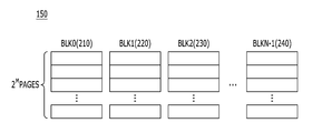
우선, 도 2를 참조하면, 메모리 장치(150)는, 복수의 메모리 블록들, 예컨대 블록0(BLK0)(210), 블록1(BLK1)(220), 블록2(BLK2)(230), 및 블록N-1(BLKN-1)(240)을 포함하며, 각각의 블록들(210,220,230,240)은, 복수의 페이지들(Pages), 예컨대 2M개의 페이지들(2MPAGES)을 포함한다. 여기서, 설명의 편의를 위해, 복수의 메모리 블록들이 각각 2M개의 페이지들을 포함하는 것을 일 예로 하여 설명하지만, 복수의 메모리들은, 각각 M개의 페이지들을 포함할 수도 있다. 그리고, 각각의 페이지들은, 복수의 워드라인(WL: Word Line)들이 연결된 복수의 메모리 셀들을 포함한다.2,
또한, 메모리 장치(150)는, 복수의 메모리 블록들을, 하나의 메모리 셀에 저장 또는 표현할 수 있는 비트의 수에 따라, 단일 레벨 셀(SLC: Single Level Cell) 메모리 블록 및 멀티 레벨 셀(MLC: Multi Level Cell) 메모리 블록 등으로 포함할 수 있다. 여기서, SLC 메모리 블록은, 하나의 메모리 셀에 1 비트 데이터를 저장하는 메모리 셀들에 의해 구현된 복수의 페이지들을 포함하며, 데이터 연산 성능이 빠르며 내구성이 높다. 그리고, MLC 메모리 블록은, 하나의 메모리 셀에 멀티 비트 데이터(예를 들면, 2 비트 이상)를 저장하는 메모리 셀들에 의해 구현된 복수의 페이지들을 포함하며, SLC 메모리 블록보다 큰 데이터 저장 공간을 가질 수, 다시 말해 고집적화 할 수 있다. 여기서, 하나의 메모리 셀에 3 비트 데이터를 저장할 수 있는 메모리 셀들에 의해 구현된 복수의 페이지들을 포함하는 MLC 메모리 블록을, 트리플 레벨 셀(TLC: Triple Level Cell) 메모리 블록으로 구분할 수도 있다.In addition, the
그리고, 각각의 블록들(210,220,230,240)은, 라이트 동작을 통해 호스트 장치로부터 제공된 데이터를 저장하고, 리드 동작을 통해 저장된 데이터를 호스트(102)로 제공한다.Each of the
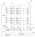
다음으로, 도 3을 참조하면, 메모리 시스템(110)에서 메모리 장치(150)의 메모리 블록(152)은, 비트라인들(BL0 to BLm-1)에 각각 연결된 복수의 셀 스트링들(340)을 포함할 수 있다. 각 열(column)의 셀 스트링(340)은, 적어도 하나의 드레인 선택 트랜지스터(DST)와, 적어도 하나의 소스 선택 트랜지스터(SST)를 포함할 수 있다. 선택 트랜지스터들(DST, SST) 사이에는, 복수 개의 메모리 셀들, 또는, 메모리 셀 트랜지스터들(MC0 to MCn-1)이 직렬로 연결될 수 있다. 각각의 메모리 셀(MC0 to MCn-1)은, 셀 당 복수의 비트의 데이터 정보를 저장하는 멀티 레벨 셀(MLC: Multi-Level Cell)로 구성될 수 있다. 셀 스트링들(340)은 대응하는 비트라인들(BL0 to BLm-1)에 각각 전기적으로 연결될 수 있다.3,
여기서, 도 3은 낸드 플래시 메모리 셀로 구성된 메모리 블록(152)을 일 예로 도시하고 있으나, 본 발명의 실시 예에 따른 메모리 장치(150)의 메모리 블록(152)은, 낸드 플래시 메모리에만 국한되는 것은 아니라 노어 플래시 메모리(NOR-type Flash memory), 적어도 두 종류 이상의 메모리 셀들이 혼합된 하이브리드 플래시 메모리, 및 메모리 칩 내에 컨트롤러가 내장된 One-NAND 플래시 메모리 등으로도 구현될 수 있다. 반도체 장치의 동작 특성은 전하 저장층이 전도성 부유 게이트로 구성된 플래시 메모리 장치는 물론, 전하 저장층이 절연막으로 구성된 차지 트랩형 플래시(Charge Trap Flash; CTF)에도 적용될 수 있다.3 illustrates a
그리고, 메모리 장치(150)의 전압 공급 회로(310)는, 동작 모드에 따라서 각각의 워드라인들로 공급될 워드라인 전압들(예를 들면, 프로그램 전압, 리드 전압, 패스 전압 등)과, 메모리 셀들이 형성된 벌크(예를 들면, 웰 영역)로 공급될 전압을 제공할 수 있으며, 이때 전압 공급 회로(310)의 전압 발생 동작은 제어 회로(도시하지 않음)의 제어에 의해 수행될 수 있다. 또한, 전압 공급 회로(310)는, 다수의 리드 데이터를 생성하기 위해 복수의 가변 리드 전압들을 생성할 수 있으며, 제어 회로의 제어에 응답하여 메모리 셀 어레이의 메모리 블록들(또는 섹터들) 중 하나를 선택하고, 선택된 메모리 블록의 워드라인들 중 하나를 선택할 수 있으며, 워드라인 전압을 선택된 워드라인 및 비선택된 워드라인들로 각각 제공할 수 있다.The
아울러, 메모리 장치(150)의 리드/라이트(read/write) 회로(320)는, 제어 회로에 의해서 제어되며, 동작 모드에 따라 감지 증폭기(sense amplifier)로서 또는 라이트 드라이버(write driver)로서 동작할 수 있다. 예를 들면, 검증/정상 리드 동작의 경우 리드/라이트 회로(320)는, 메모리 셀 어레이로부터 데이터를 리드하기 위한 감지 증폭기로서 동작할 수 있다. 또한, 프로그램 동작의 경우 리드/라이트 회로(320)는, 메모리 셀 어레이에 저장될 데이터에 따라 비트라인들을 구동하는 라이트 드라이버로서 동작할 수 있다. 리드/라이트 회로(320)는, 프로그램 동작 시 셀 어레이에 라이트될 데이터를 버퍼(미도시)로부터 수신하고, 입력된 데이터에 따라 비트라인들을 구동할 수 있다. 이를 위해, 리드/라이트 회로(320)는, 열(column)들(또는 비트라인들) 또는 열쌍(column pair)(또는 비트라인 쌍들)에 각각 대응되는 복수 개의 페이지 버퍼(PB)들(322,324,326)을 포함할 수 있으며, 각각의 페이지 버퍼(page buffer)(322,324,326)에는 복수의 래치들(도시하지 않음)이 포함될 수 있다. 그러면 여기서, 도 4 내지 도 11을 참조하여 본 발명의 실시 예에 따른 메모리 시스템에서 메모리 장치가 3차원 비휘발성 메모리 장치로 구현될 경우의 메모리 장치에 대해서 보다 구체적으로 설명하기로 한다.In addition, the read /
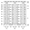
도 4를 참조하면, 메모리 장치(150)는, 전술한 바와 같이, 복수의 메모리 블록들(BLK0 to BLKN-1)을 포함할 수 있다. 여기서, 도 4는, 도 2에 도시한 메모리 장치의 메모리 블록을 보여주는 블록도로서, 각 메모리 블록(BLK)은, 3차원 구조(또는 수직 구조)로 구현될 수 있다. 예를 들면, 각 메모리 블록(BLK)은 제1방향 내지 제3방향들, 예컨대 x-축 방향, y-축 방향, 및 z-축 방향을 따라 신장된 구조물들을 포함할 수 있다.Referring to FIG. 4, the
각 메모리 블록(BLK)은 제2방향을 따라 신장된 복수의 낸드 스트링들(NS)을 포함할 수 있다. 제1방향 및 제3방향들을 따라 복수의 낸드 스트링들(NS)이 제공될 수 있다. 각 낸드 스트링(NS)은 비트라인(BL), 적어도 하나의 스트링 선택라인(SSL), 적어도 하나의 접지 선택라인(GSL), 복수의 워드라인들(WL), 적어도 하나의 더미 워드라인(DWL), 그리고 공통 소스라인(CSL)에 연결될 수 있다. 즉, 각 메모리 블록은 복수의 비트라인들(BL), 복수의 스트링 선택라인들(SSL), 복수의 접지 선택라인들(GSL), 복수의 워드라인들(WL), 복수의 더미 워드라인들(DWL), 그리고 복수의 공통 소스라인(CSL)에 연결될 수 있다.Each memory block BLK may include a plurality of NAND strings NS extending along a second direction. A plurality of NAND strings NS may be provided along the first direction and the third direction. Each NAND string NS includes a bit line BL, at least one string select line SSL, at least one ground select line GSL, a plurality of word lines WL, at least one dummy word line DWL ), And a common source line (CSL). That is, each memory block includes a plurality of bit lines BL, a plurality of string select lines SSL, a plurality of ground select lines GSL, a plurality of word lines WL, a plurality of dummy word lines (DWL), and a plurality of common source lines (CSL).
그리고, 도 5 및 도 6을 참조하면, 메모리 장치(150)의 복수의 메모리 블록들에서 임의의 메모리 블록(BLKi)은, 제1방향 내지 제3방향들을 따라 신장된 구조물들을 포함할 수 있다. 여기서, 도 5는, 본 발명의 실시 예에 따른 메모리 장치가 제1구조의 3차원 비휘발성 메모리 장치로 구현될 경우의 구조를 개략적으로 도시한 도면이며, 도 4의 복수의 메모리 블록에서 제1구조로 구현된 임의의 메모리 블록(BLKi)을 도시한 사시도이고, 도 6은, 도 5의 메모리 블록(BLKi)을 임의의 제1선(I-I')에 따른 단면도이다.5 and 6, an arbitrary memory block BLKi in the plurality of memory blocks of the
우선, 기판(5111)이 제공될 수 있다. 예컨대, 기판(5111)은 제1타입 불순물로 도핑된 실리콘 물질을 포함할 수 있다. 예를 들면, 기판(5111)은 p-타입 불순물로 도핑된 실리콘 물질을 포함하거나, p-타입 웰(예를 들면, 포켓 p-웰)일 수 있고, p-타입 웰을 둘러싸는 n-타입 웰을 더 포함할 수 있다. 이하에서는 설명의 편의를 위해, 기판(5111)은 p-타입 실리콘인 것으로 가정하지만, 기판(5111)은 p-타입 실리콘으로 한정되지 않는다.First, a
그리고, 기판(5111) 상에, 제1방향을 따라 신장된 복수의 도핑 영역들(5311,5312,5313,5314)이 제공될 수 있다. 예를 들면, 복수의 도핑 영역들((5311,5312,5313,5314)은 기판(1111)과 상이한 제2타입을 가질 수 있다. 예를 들면, 복수의 도핑 영역들(5311,5312,5313,5314)은 n-타입을 가질 수 있다. 이하에서는 설명의 편의를 위해, 제1도핑 영역 내지 제4도핑 영역들(5311,5312,5313,5314)은, n-타입인 것으로 가정하지만, 제1도핑 영역 내지 제4도핑 영역들(5311,5312,5313,5314)은 n-타입인 것으로 한정되지 않는다.Then, on the
제1도핑 영역 및 제2도핑 영역들(5311,5312) 사이에 대응하는 기판(5111) 상의 영역에서, 제1방향을 따라 신장되는 복수의 절연 물질들(5112)이 제2방향을 따라 순차적으로 제공될 수 있다. 예를 들면, 복수의 절연 물질들(5112) 및 기판(5111)은 제2방향을 따라 미리 설정된 거리만큼 이격되어 제공될 수 있다. 예를 들면, 복수의 절연 물질들(5112)은 각각 제2방향을 따라 미리 설정된 거리만큼 이격되어 제공될 수 있다. 예컨대, 절연 물질들(5112)은 실리콘 산화물(Silicon Oxide)과 같은 절연 물질을 포함할 수 있다.In a region on the
제1도핑 영역 및 제2도핑 영역들(5311,5312) 사이에 대응하는 기판(5111) 상의 영역에서, 제1방향을 따라 순차적으로 배치되며 제2방향을 따라 절연 물질들(5112)을 관통하는 복수의 필라들(5113)이 제공될 수 있다. 예컨대, 복수의 필라들(5113) 각각은 절연 물질들(5112)을 관통하여 기판(5111)과 연결될 수 있다. 예컨대, 각 필라(5113)는 복수의 물질들로 구성될 수 있다. 예를 들면, 각 필라(1113)의 표면층(1114)은 제1타입으로 도핑된 실리콘 물질을 포함할 수 있다. 예를 들면, 각 필라(5113)의 표면층(5114)은 기판(5111)과 동일한 타입으로 도핑된 실리콘 물질을 포함할 수 있다. 이하에서는 설명의 편의를 위해, 각 필라(5113)의 표면층(5114)은 p-타입 실리콘을 포함하는 것으로 가정하지만, 각 필라(5113)의 표면층(5114)은 p-타입 실리콘을 포함하는 것으로 한정되지 않는다.Are sequentially disposed along the first direction in the region on the
각 필라(5113)의 내부층(5115)은 절연 물질로 구성될 수 있다. 예를 들면, 각 필라(5113)의 내부층(5115)은 실리콘 산화물(Silicon Oxide)과 같은 절연 물질로 충진될 수 있다.The
제1도핑 영역 및 제2도핑 영역들(5311,5312) 사이의 영역에서, 절연 물질들(5112), 필라들(5113), 그리고 기판(5111)의 노출된 표면을 따라 절연막(5116)이 제공될 수 있다. 예컨대, 절연막(5116)의 두께는 절연 물질들(5112) 사이의 거리의 1/2 보다 작을 수 있다. 즉, 절연 물질들(5112) 중 제1절연 물질의 하부 면에 제공된 절연막(5116), 그리고, 제1절연 물질 하부의 제2절연 물질의 상부 면에 제공된 절연막(5116) 사이에, 절연 물질들(5112) 및 절연막(5116) 이외의 물질이 배치될 수 있는 영역이 제공될 수 있다.The insulating
제1도핑 영역 및 제2도핑 영역들(5311,5312) 사이의 영역에서, 절연막(5116)의 노출된 표면 상에 도전 물질들(5211,5221,5231,5241,5251,5261,5271,5281,5291)이 제공될 수 있다. 예를 들면, 기판(5111)에 인접한 절연 물질(5112) 및 기판(5111) 사이에 제1방향을 따라 신장되는 도전 물질(5211)이 제공될 수 있다. 특히, 기판(5111)에 인접한 절연 물질(5112)의 하부 면의 절연막(5116) 및 기판(5111)의 상부 면의 절연막(5116) 사이에, 제1방향으로 신장되는 도전 물질(5211)이 제공될 수 있다.In the region between the first doped region and the second
절연 물질들(5112) 중 특정 절연 물질 상부 면의 절연막(5116) 및 특정 절연 물질 상부에 배치된 절연 물질의 하부 면의 절연막(5116) 사이에, 제1방향을 따라 신장되는 도전 물질이 제공될 수 있다. 예컨대, 절연 물질들(5112) 사이에, 제1방향으로 신장되는 복수의 도전 물질들(5221,5231,5241,5251,5261,5271,5281)이 제공될 수 있다. 또한, 최상부 절연 물질(5112) 상의 영역에 제1방향을 따라 신장되는 도전 물질(5291)이 제공될 수 있다. 예컨대, 제1방향으로 신장된 도전 물질들(5211,5221,5231,5241,5251,5261,5271,5281,5291)은 금속 물질일 수 있다. 예컨대, 제1방향으로 신장된 도전 물질들(5211,5221,5231,5241,5251,5261,5271,5281,5291)은 폴리 실리콘 등과 같은 도전 물질일 수 있다.A conductive material extending along the first direction is provided between the insulating
제2도핑 영역 및 제3도핑 영역들(5312,5313) 사이의 영역에서, 제1도핑 영역 및 제2도핑 영역들(5311,5312) 사이의 구조물과 동일한 구조물이 제공될 수 있다. 예컨대, 제2도핑 영역 및 제3도핑 영역들(5312,5313) 사이의 영역에서, 제1방향으로 신장되는 복수의 절연 물질들(5112), 제1방향을 따라 순차적으로 배치되며 제3방향을 따라 복수의 절연 물질들(5112)을 관통하는 복수의 필라들(5113), 복수의 절연 물질들(5112) 및 복수의 필라들(5113)의 노출된 표면에 제공되는 절연막(5116), 그리고, 제1방향을 따라 신장되는 복수의 도전 물질들(5212,5222,5232,5242,5252,5262,5272,5282,5292)이 제공될 수 있다.In the region between the second doped region and the third
제3도핑 영역 및 제4도핑 영역들(5313,5314) 사이의 영역에서, 제1도핑 영역 및 제2도핑 영역들(5311,5312) 사이의 구조물과 동일한 구조물이 제공될 수 있다. 예컨대, 제3도핑 영역 및 제4도핑 영역들(5312,5313) 사이의 영역에서, 제1방향으로 신장되는 복수의 절연 물질들(5112), 제1방향을 따라 순차적으로 배치되며 제3방향을 따라 복수의 절연 물질들(5112)을 관통하는 복수의 필라들(5113), 복수의 절연 물질들(5112) 및 복수의 필라들(5113)의 노출된 표면에 제공되는 절연막(5116), 그리고 제1방향을 따라 신장되는 복수의 도전 물질들(5213,5223,5243,5253,5263,5273,5283,5293)이 제공될 수 있다.In the region between the third doped region and the fourth
복수의 필라들(5113) 상에 드레인들(5320)이 각각 제공될 수 있다. 예컨대, 드레인들(5320)은 제2타입으로 도핑된 실리콘 물질들일 수 있다. 예를 들면, 드레인들(5320)은 n-타입으로 도핑된 실리콘 물질들일 수 있다. 이하에서는 설명의 편의를 위해, 드레인들(5320)는 n-타입 실리콘을 포함하는 것으로 가정하지만, 드레인들(5320)은 n-타입 실리콘을 포함하는 것으로 한정되지 않는다. 예컨대, 각 드레인(5320)의 폭은 대응하는 필라(5113)의 폭 보다 클 수 있다. 예를 들면, 각 드레인(5320)은 대응하는 필라(5113)의 상부면에 패드 형태로 제공될 수 있다.
드레인들(5320) 상에, 제3방향으로 신장된 도전 물질들(5331,5332,5333)이 제공될 수 있다. 도전 물질들(5331,5332,5333)은 제1방향을 따라 순차적으로 배치될 수 있다. 도전 물질들(5331,5332,5333) 각각은 대응하는 영역의 드레인들(5320)과 연결될 수 있다. 예컨대, 드레인들(5320) 및 제3방향으로 신장된 도전 물질들(5331,5332,5333)은 각각 콘택 플러그들(contact plug)을 통해 연결될 수 있다. 예컨대, 제3방향으로 신장된 도전 물질들(5331,5332,5333)은 금속 물질일 수 있다. 예컨대, 제3방향으로 신장된 도전 물질들(5331,5332,53333)은 폴리 실리콘 등과 같은 도전 물질일 수 있다.On the
도 5 및 도 6에서, 각 필라(5113)는 절연막(5116)의 인접한 영역 및 제1방향을 따라 신장되는 복수의 도체라인들(5211 내지 5291, 5212 내지 5292, 및 5213 내지 5293) 중 인접한 영역과 함께 스트링을 형성할 수 있다. 예를 들면, 각 필라(5113)는 절연막(5116)의 인접한 영역 및 제1방향을 따라 신장되는 복수의 도체라인들(5211 내지 5291, 5212 내지 5292, 및 5213 내지 5293) 중 인접한 영역과 함께 낸드 스트링(NS)을 형성할 수 있다. 낸드 스트링(NS)은 복수의 트랜지스터 구조들(TS)을 포함할 수 있다.5 and 6, each of the
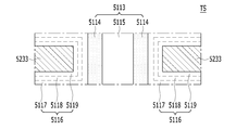
그리고, 도 7을 참조하면, 도 6에 도시한 트랜지스터 구조(TS)에서의 절연막(5116)은, 제1서브 절연막 내지 제3서브 절연막들(5117,5118,5119)을 포함할 수 있다. 여기서, 도 7은, 도 6의 트랜지스터 구조(TS)를 보여주는 단면도이다.7, the insulating
필라(5113)의 p-타입 실리콘(5114)은 바디(body)로 동작할 수 있다. 필라(5113)에 인접한 제1서브 절연막(5117)은 터널링 절연막으로 동작할 수 있으며, 열산화막을 포함할 수 있다.The p-
제2서브 절연막(5118)은 전하 저장막으로 동작할 수 있다. 예를 들면, 제2서브 절연막(5118)은 전하 포획층으로 동작할 수 있으며, 질화막 또는 금속 산화막(예컨대, 알루미늄 산화막, 하프늄 산화막 등)을 포함할 수 있다.The
도전 물질(5233)에 인접한 제3 서브 절연막(5119)은 블로킹 절연막으로 동작할 수 있다. 예를 들면, 제1방향으로 신장된 도전 물질(5233)과 인접한 제3서브 절연막(5119)은 단일층 또는 다층으로 형성될 수 있다. 제3서브 절연막(5119)은 제1서브 절연막 및 제2서브 절연막들(5117,5118)보다 높은 유전상수를 갖는 고유전막(예컨대, 알루미늄 산화막, 하프늄 산화막 등)일 수 있다.The
도전 물질(5233)은 게이트(또는 제어 게이트)로 동작할 수 있다. 즉, 게이트(또는 제어 게이트(5233)), 블로킹 절연막(5119), 전하 저장막(5118), 터널링 절연막(5117), 및 바디(5114)는, 트랜지스터(또는 메모리 셀 트랜지스터 구조)를 형성할 수 있다. 예컨대, 제1서브 절연막 내지 제3서브 절연막들(5117,5118,5119)은 ONO(oxide-nitride-oxide)를 구성할 수 있다. 이하에서는 설명의 편의를 위해, 필라(5113)의 p-타입 실리콘(5114)을 제2방향의 바디라 칭하기로 한다.
메모리 블록(BLKi)은 복수의 필라들(5113)을 포함할 수 있다. 즉, 메모리 블록(BLKi)은 복수의 낸드 스트링들(NS)을 포함할 수 있다. 보다 구체적으로 설명하면, 메모리 블록(BLKi)은 제2방향(또는 기판과 수직한 방향)으로 신장된 복수의 낸드 스트링들(NS)을 포함할 수 있다.The memory block BLKi may include a plurality of
각 낸드 스트링(NS)은 제2방향을 따라 배치되는 복수의 트랜지스터 구조들(TS)을 포함할 수 있다. 각 낸드 스트링(NS)의 복수의 트랜지스터 구조들(TS) 중 적어도 하나는 스트링 선택 트랜지스터(SST)로 동작할 수 있다. 각 낸드 스트링(NS)의 복수의 트랜지스터 구조들(TS) 중 적어도 하나는 접지 선택 트랜지스터(GST)로 동작할 수 있다.Each NAND string NS may include a plurality of transistor structures TS disposed along a second direction. At least one of the plurality of transistor structures TS of each NAND string NS may operate as a string selection transistor (SST). At least one of the plurality of transistor structures TS of each NAND string NS may operate as a ground selection transistor (GST).
게이트들(또는 제어 게이트들)은 제1방향으로 신장된 도전 물질들(5211 내지 5291, 5212 내지 5292, 및 5213 내지 5293)에 대응할 수 있다. 즉, 게이트들(또는 제어 게이트들)은 제1방향으로 신장되어 워드라인들, 그리고 적어도 두 개의 선택라인들(예를 들면, 적어도 하나의 스트링 선택라인(SSL) 및 적어도 하나의 접지 선택라인(GSL))을 형성할 수 있다.The gates (or control gates) may correspond to the
제3방향으로 신장된 도전 물질들(5331,5332,5333)은 낸드 스트링들(NS)의 일단에 연결될 수 있다. 예컨대, 제3방향으로 신장된 도전 물질들(5331,5332,5333)은 비트라인들(BL)로 동작할 수 있다. 즉, 하나의 메모리 블록(BLKi)에서, 하나의 비트라인(BL)에 복수의 낸드 스트링들(NS)이 연결될 수 있다.The
제1방향으로 신장된 제2타입 도핑 영역들(5311,5312,5313,5314)이 낸드 스트링들(NS)의 타단에 제공될 수 있다. 제1방향으로 신장된 제2타입 도핑 영역들(5311,5312,5313,5314)은 공통 소스라인들(CSL)로 동작할 수 있다.Second type doped
즉, 메모리 블록(BLKi)은 기판(5111)에 수직한 방향(제2방향)으로 신장된 복수의 낸드 스트링들(NS)을 포함하며, 하나의 비트라인(BL)에 복수의 낸드 스트링들(NS)이 연결되는 낸드 플래시 메모리 블록(예를 들면, 전하 포획형)으로 동작할 수 있다.That is, the memory block BLKi includes a plurality of NAND strings NS extending in a direction perpendicular to the substrate 5111 (second direction), and a plurality of NAND strings NAND flash memory block (e.g., charge trapping type) to which the NAND flash memory is connected.
도 5 내지 도 7에서는, 제1방향으로 신장되는 도체라인들(5211 내지 5291, 5212 내지 5292, 및 5213 내지 5293)이 9개의 층에 제공되는 것으로 설명하였지만, 제1방향으로 신장되는 도체라인들(5211 내지 5291, 5212 내지 5292, 및 5213 내지 5293)이 9개의 층에 제공되는 것으로 한정되지 않는다. 예를 들면, 제1방향으로 신장되는 도체라인들은 8개의 층, 16개의 층, 또는 복수의 층에 제공될 수 있다. 즉, 하나의 낸드 스트링(NS)에서, 트랜지스터는 8개, 16개, 또는 복수 개일 수 있다.5 to 7,
전술한 도 5 내지 도 7에서는, 하나의 비트라인(BL)에 3 개의 낸드 스트링들(NS)이 연결되는 것으로 설명하였으나, 하나의 비트라인(BL)에 3개의 낸드 스트링들(NS)이 연결되는 것으로 한정되지 않는다. 예컨대, 메모리 블록(BLKi)에서, 하나의 비트라인(BL)에 m 개의 낸드 스트링들(NS)이 연결될 수 있다. 이때, 하나의 비트라인(BL)에 연결되는 낸드 스트링들(NS)의 수만큼, 제1방향으로 신장되는 도전 물질들(5211 내지 5291, 5212 내지 5292, 및 5213 내지 5293)의 수 및 공통 소스라인들(5311,5312,5313,5314)의 수 또한 조절될 수 있다.5 to 7, three NAND strings NS are connected to one bit line BL. However, three NAND strings NS may be connected to one bit line BL, . For example, in the memory block BLKi, m NAND strings NS may be connected to one bit line BL. At this time, the number of conductive materials (5211 to 5291, 5212 to 5292, and 5213 to 5293) extending in the first direction by the number of NAND strings (NS) connected to one bit line (BL) The number of
또한, 도 5 내지 도 7에서는, 제1방향으로 신장된 하나의 도전 물질에 3 개의 낸드 스트링들(NS)이 연결되는 것으로 설명하였으나, 제1방향으로 신장된 하나의 도전 물질에 3 개의 낸드 스트링들(NS)이 연결되는 것으로 한정되지 않는다. 예를 들면, 제1방향으로 신장된 하나의 도전 물질에, n 개의 낸드 스트링들(NS)이 연결될 수 있다. 이때, 제1방향으로 신장된 하나의 도전 물질에 연결되는 낸드 스트링들(NS)의 수만큼, 비트라인들(5331,5332,5333)의 수 또한 조절될 수 있다.5 to 7, three NAND strings NS are connected to one conductive material extending in the first direction. However, in the case where one conductive material extended in the first direction has three NAND strings NS are connected to each other. For example, n conductive n-strings NS may be connected to one conductive material extending in a first direction. At this time, the number of
도 8을 참조하면, 메모리 장치(150)의 복수의 블록들에서 제1구조로 구현된 임의의 블록(BLKi)에는, 제1비트라인(BL1) 및 공통 소스라인(CSL) 사이에 낸드 스트링들(NS11 to NS31)이 제공될 수 있다. 여기서, 도 8은, 도 5 내지 도 7에서 설명한 제1구조로 구현된 메모리 블록(BLKi)의 등가 회로를 도시한 회로도이다. 그리고, 제1비트라인(BL1)은 제3방향으로 신장된 도전 물질(5331)에 대응할 수 있다. 제2비트라인(BL2) 및 공통 소스라인(CSL) 사이에 낸드 스트링들(NS12, NS22, NS32)이 제공될 수 있다. 제2비트라인(BL2)은 제3방향으로 신장된 도전 물질(5332)에 대응할 수 있다. 제3비트라인(BL3) 및 공통 소스라인(CSL) 사이에, 낸드 스트링들(NS13, NS23, NS33)이 제공될 수 있다. 제3비트라인(BL3)은 제3방향으로 신장된 도전 물질(5333)에 대응할 수 있다.8, in any block BLKi implemented with the first structure in the plurality of blocks of the
각 낸드 스트링(NS)의 스트링 선택 트랜지스터(SST)는 대응하는 비트라인(BL)과 연결될 수 있다. 각 낸드 스트링(NS)의 접지 선택 트랜지스터(GST)는 공통 소스라인(CSL)과 연결될 수 있다. 각 낸드 스트링(NS)의 스트링 선택 트랜지스터(SST) 및 접지 선택 트랜지스터(GST) 사이에 메모리 셀들(MC)이 제공될 수 있다.The string selection transistor SST of each NAND string NS may be connected to the corresponding bit line BL. The ground selection transistor GST of each NAND string NS can be connected to the common source line CSL. Memory cells MC may be provided between the string selection transistor SST and the ground selection transistor GST of each NAND string NS.
이하에서는 설명의 편의를 위해, 행(row) 및 열(column)) 단위로 낸드 스트링들(NS)을 정의할 수 있으며, 하나의 비트라인에 공통으로 연결된 낸드 스트링들(NS)은 하나의 열을 형성할 수 있음을, 일 예로 하여 설명하기로 한다. 예를 들면, 제1비트라인(BL1)에 연결된 낸드 스트링들(NS11 내지 NS31)은 제1열에 대응할 수 있고, 제2비트라인(BL2)에 연결된 낸드 스트링들(NS12 내지 NS32)은 제2열에 대응할 수 있으며, 제3비트라인(BL3)에 연결된 낸드 스트링들(NS13 내지 NS33)은 제3열에 대응할 수 있다. 하나의 스트링 선택라인(SSL)에 연결되는 낸드 스트링들(NS)은 하나의 행을 형성할 수 있다. 예를 들면, 제1스트링 선택라인(SSL1)에 연결된 낸드 스트링들(NS11 내지 NS13)은 제1행을 형성할 수 있고, 제2스트링 선택라인(SSL2)에 연결된 낸드 스트링들(NS21 내지 NS23)은 제2행을 형성할 수 있으며, 제3스트링 선택라인(SSL3)에 연결된 낸드 스트링들(NS31 내지 NS33)은 제3행을 형성할 수 있다.Hereinafter, for convenience of explanation, NAND strings NS may be defined in units of a row and a column, and NAND strings NS connected in common to one bit line may be defined as one column As will be described below. For example, the NAND strings NS11 to NS31 connected to the first bit line BL1 may correspond to the first column, and the NAND strings NS12 to NS32 connected to the second bit line BL2 may correspond to the second column And the NAND strings NS13 to NS33 connected to the third bit line BL3 may correspond to the third column. The NAND strings NS connected to one string select line (SSL) can form one row. For example, the NAND strings NS11 through NS13 connected to the first string selection line SSL1 may form a first row, the NAND strings NS21 through NS23 connected to the second string selection line SSL2, And the NAND strings NS31 to NS33 connected to the third string selection line SSL3 may form the third row.
또한, 각 낸드 스트링(NS)에서, 높이가 정의될 수 있다. 예컨대, 각 낸드 스트링(NS)에서, 접지 선택 트랜지스터(GST)에 인접한 메모리 셀(MC1)의 높이는 1이다. 각 낸드 스트링(NS)에서, 스트링 선택 트랜지스터(SST)에 인접할수록 메모리 셀의 높이는 증가할 수 있다. 각 낸드 스트링(NS)에서, 스트링 선택 트랜지스터(SST)에 인접한 메모리 셀(MC6)의 높이는 7이다.Further, in each NAND string NS, a height can be defined. For example, in each NAND string NS, the height of the memory cell MC1 adjacent to the ground selection transistor GST is one. In each NAND string NS, the height of the memory cell may increase as the string selection transistor SST is adjacent to the string selection transistor SST. In each NAND string NS, the height of the memory cell MC6 adjacent to the string selection transistor SST is seven.
그리고, 동일한 행의 낸드 스트링들(NS)의 스트링 선택 트랜지스터들(SST)은 스트링 선택라인(SSL)을 공유할 수 있다. 상이한 행의 낸드 스트링들(NS)의 스트링 선택 트랜지스터들(SST)은 상이한 스트링 선택라인들(SSL1, SSL2, SSL3)에 각각 연결될 수 있다.Then, the string selection transistors SST of the NAND strings NS in the same row can share the string selection line SSL. The string selection transistors SST of the NAND strings NS of the different rows can be connected to the different string selection lines SSL1, SSL2 and SSL3, respectively.
아울러, 동일한 행의 낸드 스트링들(NS)의 동일한 높이의 메모리 셀들은 워드라인(WL)을 공유할 수 있다. 또한, 동일한 높이에서, 상이한 행의 낸드 스트링들(NS)의 메모리 셀들(MC)에 연결된 워드라인들(WL)은 공통으로 연결될 수 있다. 동일한 행의 낸드 스트링들(NS)의 동일한 높이의 더미 메모리 셀들(DMC)은 더미 워드라인(DWL)을 공유할 수 있다. 또한, 동일한 높이에서, 상이한 행의 낸드 스트링들(NS)의 더미 메모리 셀들(DMC)에 연결된 더미 워드라인들(DWL)은 공통으로 연결될 수 있다.In addition, memory cells at the same height of the NAND strings NS in the same row can share the word line WL. Further, at the same height, the word lines WL connected to the memory cells MC of the NAND strings NS of different rows can be connected in common. The dummy memory cells DMC of the same height of the NAND strings NS in the same row can share the dummy word line DWL. Further, at the same height, the dummy word lines DWL connected to the dummy memory cells DMC of the NAND strings NS of the different rows can be connected in common.
예컨대, 워드라인들(WL) 또는 더미 워드라인들(DWL)은 제1방향으로 신장되는 도전 물질들(5211 내지 5291, 5212 내지 5292, 및 5213 내지 5293)이 제공되는 층에서 공통으로 연결될 수 있다. 예컨대, 제1방향으로 신장되는 도전 물질들(5211 내지 5291, 5212 내지 5292, 및 5213 내지 5293)은 콘택을 통해 상부 층에 연결될 수 있다. 상부 층에서 제1방향으로 신장되는 도전 물질들(5211 내지 5291, 5212 내지 5292, 및 5213 내지 5293)이 공통으로 연결될 수 있다. 즉, 동일한 행의 낸드 스트링들(NS)의 접지 선택 트랜지스터들(GST)은 접지 선택라인(GSL)을 공유할 수 있다. 그리고, 상이한 행의 낸드 스트링들(NS)의 접지 선택 트랜지스터들(GST)은 접지 선택라인(GSL)을 공유할 수 있다. 다시 말해, 낸드 스트링들(NS11 내지 NS13, NS21 내지 NS23, 및 NS31 내지 NS33)은 접지 선택라인(GSL)에 공통으로 연결될 수 있다.For example, the word lines WL or the dummy word lines DWL may be connected in common in the layer provided with the
공통 소스라인(CSL)은 낸드 스트링들(NS)에 공통으로 연결될 수 있다. 예를 들면, 기판(5111) 상의 활성 영역에서, 제1도핑 영역 내지 제4도핑 영역들(5311,5312,5313,5314)이 연결될 수 있다. 예를 들면, 제1도핑 영역 내지 제4도핑 영역들(5311,5312,5313,5314)은 콘택을 통해 상부 층에 연결될 수 있고, 또한 상부 층에서 제1도핑 영역 내지 제4도핑 영역들(5311,5312,5313,5314)이 공통으로 연결될 수 있다.The common source line CSL may be connected in common to the NAND strings NS. For example, in the active region on the
즉, 도 8에 도시된 바와 같이, 동일 깊이의 워드라인들(WL)은 공통으로 연결될 수 있다. 따라서, 특정 워드라인(WL)이 선택될 때, 특정 워드라인(WL)에 연결된 모든 낸드 스트링들(NS)이 선택될 수 있다. 상이한 행의 낸드 스트링들(NS)은 상이한 스트링 선택라인(SSL)에 연결될 수 있다. 따라서, 스트링 선택라인들(SSL1 내지 SSL3)을 선택함으로써, 동일 워드라인(WL)에 연결된 낸드 스트링들(NS) 중 비선택 행의 낸드 스트링들(NS)이 비트라인들(BL1 내지 BL3)로부터 분리될 수 있다. 즉, 스트링 선택라인들(SSL1 내지 SSL3)을 선택함으로써, 낸드 스트링들(NS)의 행이 선택될 수 있다. 그리고, 비트라인들(BL1 내지 BL3)을 선택함으로써, 선택 행의 낸드 스트링들(NS)이 열 단위로 선택될 수 있다.That is, as shown in FIG. 8, the word lines WL of the same depth can be connected in common. Thus, when a particular word line WL is selected, all NAND strings NS connected to a particular word line WL can be selected. NAND strings NS in different rows may be connected to different string select lines SSL. Thus, by selecting the string selection lines SSL1 to SSL3, the NAND strings NS of unselected rows among the NAND strings NS connected to the same word line WL are selected from the bit lines BL1 to BL3 Can be separated. That is, by selecting the string selection lines SSL1 to SSL3, a row of NAND strings NS can be selected. Then, by selecting the bit lines BL1 to BL3, the NAND strings NS of the selected row can be selected in units of columns.
각 낸드 스트링(NS)에서, 더미 메모리 셀(DMC)이 제공될 수 있다. 더미 메모리 셀(DMC) 및 접지 선택 트랜지스터(GST) 사이에 제1메모리 셀 내지 제3메모리 셀들(MC1 내지 MC3)이 제공될 수 있다.In each NAND string NS, a dummy memory cell DMC may be provided. The first to third memory cells MC1 to MC3 may be provided between the dummy memory cell DMC and the ground selection transistor GST.
더미 메모리 셀(DMC) 및 스트링 선택 트랜지스터(SST) 사이에 제4메모리 셀 내지 제6메모리 셀들(MC4 내지 MC6)이 제공될 수 있다. 여기서, 각 낸드 스트링(NS)의 메모리 셀들(MC)은, 더미 메모리 셀(DMC)에 의해 메모리 셀 그룹들로 분할될 수 있으며, 분할된 메모리 셀 그룹들 중 접지 선택 트랜지스터(GST)에 인접한 메모리 셀들(예를 들면, MC1 to MC3)을 하부 메모리 셀 그룹이라 할 수 있고, 분할된 메모리 셀 그룹들 중 스트링 선택 트랜지스터(SST)에 인접한 메모리 셀들(예를 들면, MC4 내지 MC6)을 상부 메모리 셀 그룹이라 할 수 있다. 그러면 이하에서는, 도 9 내지 도 11을 참조하여 본 발명의 실시 예에 따른 메모리 시스템에서 메모리 장치가 제1구조와 다른 구조의 3차원 비휘발성 메모리 장치로 구현될 경우에 대해 보다 구체적으로 설명하기로 한다.The fourth to sixth memory cells MC4 to MC6 may be provided between the dummy memory cell DMC and the string selection transistor SST. Here, the memory cells MC of each NAND string NS can be divided into memory cell groups by the dummy memory cells DMC, and the memory cells MC of the divided memory cell groups adjacent to the ground selection transistor GST (For example, MC1 to MC3) may be referred to as a lower memory cell group, and memory cells (for example, MC4 to MC6) adjacent to the string selection transistor SST among the divided memory cell groups may be referred to as an upper memory cell Group. Hereinafter, with reference to FIGS. 9 to 11, the memory device according to the embodiment of the present invention will be described in more detail when the memory device is implemented as a three-dimensional nonvolatile memory device having a structure different from that of the first structure do.
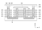
도 9 및 도 10을 참조하면, 메모리 장치(150)의 복수의 메모리 블록들에서 제2구조로 구현된 임의의 메모리 블록(BLKj)은, 제1방향 내지 제3방향들을 따라 신장된 구조물들을 포함할 수 있다. 여기서, 도 9는, 본 발명의 실시 예에 따른 메모리 장치가 앞선 도 5 내지 도 8에서 설명한 제1구조와 다른 제2구조의 3차원 비휘발성 메모리 장치로 구현될 경우의 구조를 개략적으로 도시한 도면이며, 도 4의 복수의 메모리 블록에서 제2구조로 구현된 임의의 메모리 블록(BLKj)을 도시한 사시도이고, 도 10은, 도 9의 메모리 블록(BLKj)을 임의의 제2선(Ⅶ-Ⅶ')에 따른 단면도이다.9 and 10, an arbitrary memory block BLKj implemented in the second structure in the plurality of memory blocks of the
우선, 기판(6311)이 제공될 수 있다. 예컨대, 기판(6311)은 제1타입 불순물로 도핑된 실리콘 물질을 포함할 수 있다. 예를 들면, 기판(6311)은 p-타입 불순물로 도핑된 실리콘 물질을 포함하거나, p-타입 웰(예를 들면, 포켓 p-웰)일 수 있고, p-타입 웰을 둘러싸는 n-타입 웰을 더 포함할 수 있다. 이하에서는 설명의 편의를 위해, 기판(6311)은 p-타입 실리콘인 것으로 가정하지만, 기판(6311)은 p-타입 실리콘으로 한정되지 않는다.First, a
그리고, 기판(6311) 상에, x-축 방향 및 y-축 방향으로 신장되는 제1도전 물질 내지 제4도전 물질들(6321,6322,6323,6324)이 제공된다. 여기서, 제1도전 물질 내지 제4도전 물질들(6321,6322,6323,6324)은 z-축 방향을 따라 특정 거리만큼 이격되어 제공된다.Then, on the
또한, 기판(6311) 상에 x-축 방향 및 y-축으로 신장되는 제5도전 물질 내지 제8도전 물질들(6325,6326,6327,6328)이 제공된다. 여기서, 제5도전 물질 내지 제8도전 물질들(6325,6326,6327,6328)은 z-축 방향을 따라 특정 거리만큼 이격되어 제공된다. 그리고, 제5도전 물질 내지 제8도전 물질들(6325,6326,6327,6328)은 y-축 방향을 따라 제1도전 물질 내지 제4도전 물질들(6321,6322,6323,6324)과 이격되어 제공된다.Further, fifth to eighth
아울러, 제1도전 물질 내지 제4도전 물질들(6321,6322,6323,6324)을 관통하는 복수의 하부 필라(DP)들이 제공된다. 각 하부 필라(DP)는 z-축 방향을 따라 신장된다. 또한, 제5도전 물질 내지 제8도전 물질들(6325,6326,6327,6328)을 관통하는 복수의 상부 필라(UP)들이 제공된다. 각 상부 필라(UP)는 z-축 방향을 따라 신장된다.In addition, a plurality of lower pillars (DP) passing through the first to fourth
하부 필라(DP) 및 상부 필라(UP) 각각은 내부 물질(6361), 중간층(6362) 및 표면층(6363)을 포함한다. 여기서, 도 5 및 도 6에서 설명한 바와 같이, 중간층(6362)은 셀 트랜지스터의 채널로서 동작할 것이다. 표면층(6363)은 블로킹 절연막, 전하 저장막 및 터널링 절연막을 포함할 것이다.Each of the lower pillars DP and upper pillars UP includes an
하부 필라(DP) 및 상부 필라(UP)는 파이프 게이트(PG)를 통해 연결된다. 파이프 게이트(PG)는 기판(6311) 내에 배치될 수 있으며, 일 예로, 파이프 게이트(PG)는 하부 필라(DP) 및 상부 필라(UP)와 동일한 물질들을 포함할 수 있다.The lower pillar DP and the upper pillar UP are connected via a pipe gate PG. The pipe gate PG may be disposed within the
하부 필라(DP)의 상부에, x-축 방향 및 y-축 방향으로 신장되는 제 2 타입의 도핑 물질(6312)이 제공된다. 예컨대, 제2타입의 도핑 물질(6312)은 n-타입의 실리콘 물질을 포함할 수 있다. 제2타입의 도핑 물질(6312)은 공통 소스라인(CSL)으로서 동작한다.On top of the lower pillar DP is provided a second type of
상부 필라(UP)의 상부에 드레인(6340)이 제공된다. 예컨대, 드레인(6340)은 n-타입의 실리콘 물질을 포함할 수 있다. 그리고, 드레인(6340)들의 상부에 y-축 방향으로 신장되는 제1상부 도전 물질 및 제2상부 도전 물질들(6351,6352)이 제공된다.A
제1상부 도전 물질 및 제2상부 도전 물질들(6351,6352)은 x-축 방향을 따라 이격되어 제공된다. 예컨대, 제1상부 도전 물질 및 제2상부 도전 물질들(6351,6352)은 금속 물질로 형성될 수 있으며, 일 예로, 제1상부 도전 물질 및 제2상부 도전 물질들(6351,6352)과 드레인(6340)들은 콘택 플러그들을 통해 연결될 수 있다. 제1상부 도전 물질 및 제2상부 도전 물질들(6351,6352)은 각각 제1비트라인 및 제2비트라인들(BL1, BL2)로 동작한다.The first upper conductive material and the second upper
제1도전 물질(6321)은 소스 선택라인(SSL)으로 동작하고, 제2도전 물질(6322)은 제1더미 워드라인(DWL1)으로 동작하며, 제3도전 물질 및 제4도전 물질들(6323,6324)은 각각 제1메인 워드라인 및 제2메인 워드라인들(MWL1, MWL2)로 동작한다. 그리고, 제5도전 물질 및 제6도전 물질들(6325,6326)은 각각 제3메인 워드라인 및 제4메인 워드라인들(MWL3, MWL4)로 동작하고, 제7도전 물질(6327)은 제2더미 워드라인(DWL2)으로 동작하며, 제8도전 물질(6328)은 드레인 선택라인(DSL)로서 동작한다.The first
하부 필라(DP), 그리고 하부 필라(DP)에 인접한 제1도전 물질 내지 제4도전 물질들(6321,6322,6323,6324)은 하부 스트링을 구성한다. 상부 필라(UP), 그리고 상부 필라(UP)에 인접한 제5도전 물질 내지 제8도전 물질들(6325,6326,6327,6328)은 상부 스트링을 구성한다. 하부 스트링 및 상부 스트링은 파이프 게이트(PG)를 통해 연결된다. 하부 스트링의 일단은 공통 소스라인(CSL)으로 동작하는 제2타입의 도핑 물질(6312)에 연결된다. 상부 스트링의 일단은 드레인(6320)을 통해 해당 비트라인에 연결된다. 하나의 하부 스트링 및 하나의 상부 스트링은 제2타입의 도핑 물질(6312)과 해당 비트라인 사이에 연결된 하나의 셀 스트링을 구성할 것이다.And the first to fourth
즉, 하부 스트링은 소스 선택 트랜지스터(SST), 제1더미 메모리 셀(DMC1), 그리고 제1메인 메모리 셀 및 제2메인 메모리 셀들(MMC1, MMC2)을 포함할 것이다. 그리고, 상부 스트링은 제3메인 메모리 셀 및 제4메인 메모리 셀들(MMC3, MMC4), 제2더미 메모리 셀(DMC2), 그리고 드레인 선택 트랜지스터(DST)를 포함할 것이다.That is, the lower string will include a source select transistor (SST), a first dummy memory cell (DMC1), and a first main memory cell and a second main memory cell (MMC1, MMC2). The upper string will include a third main memory cell and fourth main memory cells MMC3 and MMC4, a second dummy memory cell DMC2, and a drain select transistor DST.
한편, 도 9 및 도 10에서 상부 스트림 및 하부 스트링은, 낸드 스트링(NS)을 형성할 수 있으며, 낸드 스트링(NS)은 복수의 트랜지스터 구조들(TS)을 포함할 수 있다. 여기서, 도 9 및 도 10에서의 낸드 스트림에 포함된 트랜지스터 구조는, 앞서 도 7에서 구체적으로 설명하였으므로, 여기서는 그에 관한 구체적인 설명을 생략하기로 한다.9 and 10, the upper stream and the lower string may form a NAND string NS, and the NAND string NS may include a plurality of transistor structures TS. Here, the transistor structure included in the NAND stream in FIGS. 9 and 10 has been described in detail with reference to FIG. 7, and a detailed description thereof will be omitted here.
그리고, 도 11을 참조하면, 메모리 장치(150)의 복수의 블록들에서 제2구조로 구현된 임의의 블록(BLKj)에는, 도 9 및 도 10에서 설명한 바와 같이, 하나의 상부 스트링과 하나의 하부 스트링이 파이프 게이트(PG)를 통해 연결되어 구현된 하나의 셀 스트링들이 각각 복수의 쌍들을 이루어 제공될 수 있다. 여기서, 도 11은, 도 9 및 도 10에서 설명한 제2구조로 구현된 메모리 블록(BLKj)의 등가 회로를 도시한 회로도이며, 설명의 편의를 위해 제2구조로 구현된 임의의 블록(BLKj)에서 한 쌍을 구성하는 제1스트링과 제2스트링만을 도시하였다.11, in an arbitrary block BLKj implemented in the second structure in the plurality of blocks of the
즉, 제2구조로 구현된 임의의 블록(BLKj)에서, 제1채널(CH1)을 따라 적층된 메모리 셀들, 예컨대 적어도 하나의 소스 선택 게이트(SSG1) 및 적어도 하나의 드레인 선택 게이트(DSG1)는, 제1스트링(ST1)을 구현하고, 제2채널(CH2)을 따라 적층된 메모리 셀들, 예컨대 적어도 하나의 소스 선택 게이트(SSG2) 및 적어도 하나의 드레인 선택 게이트(DSG2)는 제2스트링(ST2)을 구현한다.That is, in any block BLKj implemented with the second structure, the memory cells stacked along the first channel CH1, such as at least one source select gate SSG1 and at least one drain select gate DSG1, And at least one source select gate SSG2 and at least one drain select gate DSG2 that implement the first string ST1 and stacked along the second channel CH2 are coupled to the second string ST2 ).
또한, 제1스트링(ST1)과 제2스트링(ST2)은, 동일한 드레인 선택라인(DSL) 및 동일한 소스 선택라인(SSL)에 연결되며, 또한 제1스트링(ST1)은, 제1비트라인(BL1)에 연결되고, 제2스트링(ST2)은 제2비트라인(BL2)에 연결된다.The first string ST1 and the second string ST2 are connected to the same drain select line DSL and the same source select line SSL and the first string ST1 is connected to the first bit line BL1 and the second string ST2 is connected to the second bit line BL2.
여기서, 설명의 편의를 위해, 도 11에서는, 제1스트링(ST1)과 제2스트링(ST2)이 동일한 드레인 선택라인(DSL) 및 동일한 소스 선택라인(SSL)에 연결되는 경우를 일 예로 설명하였으나, 제1스트링(ST1)과 제2스트링(ST2)이 동일한 소스 선택라인(SSL) 및 동일한 비트라인(BL)에 연결되어, 제1스트링(ST1)이 제1드레인 선택라인(DSL1)에 연결되고 제2스트링(ST2)이 제2드레인 선택라인(DSL2)에 연결되거나, 또는 제1스트링(ST1)과 제2스트링(ST2)이 동일한 드레인 선택라인(DSL) 및 동일한 비트라인(BL)에 연결되어, 제1스트링(ST1)이 제1소스 선택라인(SSL1)에 연결되고 제2스트링(ST2)은 제2소스 선택라인(SDSL2)에 연결될 수도 있다.11, the case where the first string ST1 and the second string ST2 are connected to the same drain selection line DSL and the same source selection line SSL has been described as an example, , The first string ST1 and the second string ST2 are connected to the same source select line SSL and the same bit line BL so that the first string ST1 is connected to the first drain select line DSL1 And the second string ST2 is connected to the second drain select line DSL2 or the first string ST1 and the second string ST2 are connected to the same drain select line DSL and the same bit line BL The first string ST1 may be connected to the first source selection line SSL1 and the second string ST2 may be connected to the second source selection line SDSL2.
도 12는 본 발명의 실시예에 따른 메모리 시스템을 개략적으로 도시한 도면이다.12 is a diagram schematically illustrating a memory system according to an embodiment of the present invention.
도 12를 참조하면, 도 1에 도시된 메모리 시스템(110)의 구성을 참조하여 도시한 것을 알 수 있다. 즉, 본 발명의 실시예에 따른 동작을 설명하는데 필요한 구성만을 좀 더 강조하여 자세히 나타내었다. 도 12에 도시한 바와 같이, 메모리 시스템(110)은 컨트롤러(130), 및 메모리 장치(150)를 포함한다. 이때, 컨트롤러(130)의 프로세서(134), 및 메모리(144)는 각각 가비지 컬렉션(GC) 모듈(1210), 및 레지스터(1220)를 포함할 수 있다. 하지만, 본 발명이 이에 한정되는 것은 아니며, 실시예에 따라 가비지 컬렉션(GC) 모듈(1210), 및 레지스터(1220)를 별개로 구비할 수도 있다.Referring to FIG. 12, it can be seen that reference is made to the configuration of the
메모리 장치(150)가 비휘발성 메모리 장치, 일 예로 플래시 메모리로 구비될 경우 컨트롤러(130)는 메모리 장치(150)의 저장 능력(storage capacity)을 높이기 위해 가비지 컬렉션(garbage collection) 동작을 수행한다. 즉, 일정 기준 이상의 무효 데이터(invalid data)들을 포함하는 메모리 블록(예를 들면, 152)을 선택하여 상기 메모리 블록(152)의 유효 데이터(valid data)들을 다른 메모리 블록(154 or 156)으로 복사하고, 무효 데이터만을 포함하는 상기 메모리 블록(152)을 삭제하여 가비지 컬렉션 동작을 수행한다. 상기 삭제된 메모리 블록(152)은 프리 블록(free block)으로 그만큼의 데이터 저장 공간을 확보할 수 있다. When the
가비지 컬렉션(GC) 모듈(1210)은 메모리 장치(150)의 유효 데이터들을 모으고 무효 데이터들을 삭제하는 가비지 컬렉션 동작을 관리할 수 있다. 즉, 가비지 컬렉션(GC) 모듈(1210)은 메모리 블록들(152~156)의 유효/무효 페이지(valid/invalid page) 수, 프리 블록 수, 등을 포함하는 가비지 컬렉션 정보를 관리한다. 뿐만 아니라, 본 발명의 실시예에 따른 가비지 컬렉션(GC) 모듈(1210)은 메모리 블록들(152~156)의 에러 비트 정보를 바탕으로 가비지 컬렉션 동작을 관리할 수 있다. 에러 비트 정보에 대해서는 아래에 좀 더 자세히 설명하기로 한다. The garbage collection (GC)
앞서 설명한 바와 같이, 컨트롤러(130)의 ECC 유닛(138)은, 메모리 장치(150)에 저장된 데이터를 리드할 경우, 메모리 장치(150)로부터 리드된 데이터에 포함되는 에러를 검출 및 정정한다. 하지만, ECC 유닛(138)은 리드된 데이터에 포함되는 에러 비트 수가 정정 가능한 한계치 이상이면, 에러 비트를 정정할 수 없으며 해당 메모리 블록을 불량 블록(bad block)으로 처리하여 관리한다. The
따라서, 컨트롤러(130)는 하나의 메모리 블록으로부터 리드된 데이터의 에러 비트 수가 기준을 초과하였는지 여부에 따라 리드 리클레임 (read reclaim) 동작을 수행할 수 있다. 이때 기준을 초과한 메모리 블록의 데이터는 모두 리드되어 다른 메모리 블록으로 복사될 수 있다. 리드 리클레임 동작을 통해, 리텐션 특성 등이 취약해진 메모리 셀들의 데이터를 옮겨줌으로써 리드 동작 시 일어날 수 있는 디스터번스(disturbance) 등을 방지할 수 있다.Accordingly, the
본 발명의 실시예에 따른 가비지 컬렉션(GC) 모듈(1210)은 이와 같은 에러 비트 정보를 가비지 컬렉션 정보와 조합하여 관리할 수 있다. 즉, 단순히 여유 공간을 확보하는 가비지 컬렉션 동작 시에 특성이 취약해진 공간을 함께 정리할 수 있다. 따라서, 메모리 장치(150)를 구동하기 위한 컨트롤러(130)의 오버헤드(overhead)를 줄이고, 메모리 장치(150)의 동작 속도 또한 향상시킬 수 있다. 본 발명의 실시예에 따른 메모리 시스템(110)의 자세한 동작은 도 15를 참조하여 후술하기로 한다. The garbage collection (GC)
도 13은 도 12의 메모리 장치(150)의 에러 비트 정보를 검출하는 동작을 설명하기 위한 도면이다.FIG. 13 is a diagram for explaining an operation of detecting error bit information in the
도 13을 참조하면, 도 3에 도시된 메모리 장치(150)의 구성을 참조하여 도시한 것을 알 수 있다. 즉, 도 3의 메모리 장치(150)의 구성을 바탕으로, 본 발명의 실시예에 따라 제어 회로(1310), 및 패스/페일 체크 회로(1320)가 추가로 구비될 수 있다.Referring to FIG. 13, it can be seen that the configuration of the
본 발명의 실시에에 따른 메모리 장치(150)의 리드 동작 시 제어 회로(1310)는 전압 제어 신호(VC_signal), 및 버퍼 제어 신호(PB_signal)를 생성하여 전압 공급 회로(310), 및 리드/라이트 회로(320)를 각각 제어할 수 있다. The
우선, 전압 공급 회로(310)는 리드 동작시 제어 회로(1310)에서 입력되는 전압 제어 신호(VC_signal)에 응답하여 리드 전압, 및 패스 전압을 생성할 수 있다. 또한, 외부로부터 입력되는 로우 어드레스에 따라 선택된/비선택된 워드라인(WL)에 각각 리드 전압, 및 패스 전압을 인가할 수 있다. First, the
이때, 메모리 장치(150)의 리드/라이트 회로(320)는, 제어 회로(1310)에서 입력되는 버퍼 제어 신호(BP_signal)에 응답하여, 감지 증폭기(sense amplifier)로서 동작할 수 있다. 예를 들면, 전압 공급 회로(310)에 의해 선택된 워드라인(WL)에 연결된 메모리 셀들(MC)의 문턱전압 상태를 비트라인(BL)을 통해 센싱하여, 메모리 셀들(MC)에 저장된 데이터를 리드할 수 있다.At this time, the read /
패스/페일 체크 회로(1320)는 리드 동작 시 리드/라이트 회로(320)에 포함되는 페이지 버퍼(PB) 그룹별로 리드 데이터의 에러 비트 정보를 검출할 수 있다. 각 페이지 버퍼 그룹 내에 포함된 페이지 버퍼(PB)들에 저장된 리드 데이터를 바탕으로 에러 비트 여부를 검출하여 카운트한다. 카운트된 에러 비트의 수가 ECC 유닛(138)에서 보정할 수 있는 허용 비트 수보다 큰지 또는 작은지를 판단하여 패스/페일 신호(PASS/FAIL)를 출력한다. 즉, 패스/페일 체크 회로(1320)는 카운트된 에러 비트의 수가 허용 비트 수보다 같거나 작을 경우 패스 신호(PASS)를 출력하고, 카운트된 에러 비트 수가 허용 비트 수보다 클 경우 페일 신호(FAIL)를 출력한다. The path /
이때, 제어 회로(1310)는 패스/페일 체크 회로(1320)로부터 출력되는 패스/페일 신호(PASS/FAIL)에 응답해, 메모리 장치(150)의 리드 동작의 성공/실패 여부를 판단할 수 있다. 또한, 패스/페일 체크 회로(1320)로부터 카운트된 에리 비트 수를 에러 비트 정보로서 컨트롤러(130)로 제공할 수 있다. 카운트된 에러 비트 수는 리드 동작의 단위인 하나의 페이지 또는 데이터 정크에 발생된 에러 비트 수일 수 있으나, 본 발명에 이에 한정되는 것은 아니다.At this time, the
본 발명의 실시예에 따라 메모리 장치(150)로부터 에러 비트 정보를 전달받는 가비지 컬렉션(GC) 모듈(1210, 도 12)은 이를 가비지 컬렉션 정보와 함께 레지스터(1220, 도 12)에 기록하여 관리할 수 있다. 도 14를 참조하면, 가비지 컬렉션 동작 시, 가비지 컬렉션 정보와 에러 비트 정보를 관리하는 동작과 이를 바탕으로, 복수의 메모리 블록들 중 희생 블록(victim block)을 선택하는 동작이 설명되어 있다.The garbage collection (GC) module 1210 (FIG. 12) that receives error bit information from the
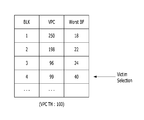
도 14는 본 발명의 실시예에 따른 가비지 컬렉션 정보와 최대 에러 비트 정보를 저장하는 관리 테이블을 도시하는 도면이다. 일실시예에 따라 관리 테이블에는 4개의 메모리 블록(BLK)의 정보가 기록되어 관리되는 것으로 나타내었으나, 본 발명이 이에 한정되는 것은 아니다. 14 is a diagram illustrating a management table for storing garbage collection information and maximum error bit information according to an embodiment of the present invention. Although it has been described that information of four memory blocks BLK is recorded and managed in the management table according to an embodiment, the present invention is not limited thereto.
관리 테이블에 저장되는 가비지 컬렉션 정보(VPC)는 유효 페이지 수롤 나타낸다. 즉 각각의 제1 내지 제4 메모리 블록들(BLK1, BLK2, BLK3, BLK4)은 250, 198, 96, 99개의 유효 페이지들을 포함하고 있는 것을 확인할 수 있다. 또한, 관리 테이블에 저장되는 최대 에러 비트 정보(Worst BF)는 기준 단위로 리드된 데이터 내에 발생한 최대 에러 비트 수를 나타낸다. 즉, 제1 내지 제4 메모리 블록들(BLK1, BLK2, BLK3, 및 BLK4)에서 리드 (또는 검증) 동작을 수행했을 때, 페이지 버퍼(PB) 그룹에서 검출되는 에러 비트 수들이 에러 비트 정보로 제공될 수 있고, 최대 에러 비트 정보(Worst BF)는 새로운 에러 비트 정보가 검출될 때마다 비교되어 더 큰 값으로 업데이트될 수 있다. (도 12의 레지스터(1220)) 각각의 정보를 바탕으로 하면, 제1 메모리 블록(BLK1)이 가장 여유 공간을 많이 확보하고 리텐션 특성도 좋은 반면, 제3 및 제4 메모리 블록(BLK3, 및 BLK4)이 각각 가장 여유 공간이 적고 리텐션 특성이 안 좋은 것을 확인할 수 있다.The garbage collection information (VPC) stored in the management table indicates the number of effective pages. That is, it can be seen that each of the first to fourth memory blocks BLK1, BLK2, BLK3, and BLK4 includes 250, 198, 96, and 99 valid pages. The maximum error bit information (Worst BF) stored in the management table represents the maximum number of error bits generated in the data read in the reference unit. That is, when the read (or verify) operation is performed in the first to fourth memory blocks BLK1, BLK2, BLK3, and BLK4, the number of error bits detected in the page buffer PB group is provided as error bit information , And the maximum error bit information (Worst BF) can be compared and updated to a larger value each time new error bit information is detected. (The register 1220 of FIG. 12), the first memory block BLK1 has the most free space and the retention characteristic is good, while the third and fourth memory blocks BLK3 and BLK3 BLK4) have the smallest free space and poor retention characteristics, respectively.
가비지 컬렉션 정보(VPC)만을 바탕으로 가비지 컬렉션 동작을 수행할 경우, 그 입계값을 100으로 설정하였을 때, 제3 및 제4 메모리 블록들(BLK3, 및 BLK4)의 유효 페이지 수가 각각 96, 99에 해당하여 희생 블록으로 선택될 수 있다. 특히, 제3 메모리 블록(BLK3)은 여유 공간이 상대적으로 더 적기 때문에, 더 많은 여유 공간 확보를 위해 제3 메모리 블록(BLK3)에 가비지 컬렉션 동작이 수행될 수 있다. When the garbage collection operation is performed based only on the garbage collection information VPC, when the threshold value is set to 100, the number of effective pages of the third and fourth memory blocks BLK3 and BLK4 is 96 and 99, respectively It can be selected as a sacrifice block. In particular, since the third memory block BLK3 has a relatively small amount of free space, a garbage collection operation can be performed on the third memory block BLK3 to secure more free space.
하지만, 메모리 블록의 특성 면에서는 최대 에러 비트 수가 더 큰 제4 메모리 블록(BLK4)이 제3 메모리 블록(BLK3)에 비해 훨씬 열악하다. 따라서 제4 메모리 블록을 우선적으로 정리하는 것이 해당 블록이 배드 블록으로 처리되는 것을 방지하고, 메모리 블록들을 보다 더 효율적으로 관리할 수 있다. 본 발명의 실시에에 따르면, 최대 에러 비트 정보(Worst BF)를 같이 참조하여 가비지 컬렉션 동작을 수행하기 때문에, 여유 공간 확보와 함께 특성이 취약해진 공간들을 정리할 수 있다.However, in terms of the characteristics of the memory block, the fourth memory block BLK4 having the largest number of error bits is much worse than the third memory block BLK3. Thus, prioritizing the fourth memory block prevents the corresponding block from being processed into the bad block, and can more efficiently manage the memory blocks. According to the embodiment of the present invention, since the garbage collection operation is performed with reference to the maximum error bit information (Worst BF), it is possible to organize the spaces in which the characteristics are weakened together with securing the free space.
이를 위해, 도 14와 같이 각각의 메모리 블록들에 대응하는 가비지 컬렉션 정보(VPC)와 에러 비트 정보(Worst BF)를 함께 저장할 수 있으나, 본 발명의 다른 실시예에 따라 일부 정보만을 저장하여 메모리(144) 공간의 효율성을 높일 수 있다. 일예로, 가비지 컬렉션 정보(VPC)가 임계값 미만인 제3 및 제4 메모리 블록만을 선택하여 에러 비트 정보를 검출하고 최대 에러 비트 정보(Worst BF)로 업데이트 할 수 있다. 더 나아가, 선택된 제3 및 제4 메모리 블록의 최대 에러 비트 정보(Worst BF) 중에서도 상위 N(N은 자연수)개의 최대 에러 비트 정보(Worst BF)만 선택하여 업데이트할 수 있다. 이때, 가비지 컬렉션 정보(VPC)가 변함에 따라 선택되는 메모리 블록들도 계속 달라질 수 있다. For this purpose, the garbage collection information (VPC) and the error bit information (Worst BF) corresponding to the respective memory blocks can be stored together as shown in FIG. 14. However, according to another embodiment of the present invention, 144) efficiency of the space can be increased. For example, only the third and fourth memory blocks whose garbage collection information (VPC) is less than the threshold value can be selected to detect error bit information and update to the maximum error bit information (Worst BF). Furthermore, only the uppermost N (N is a natural number) maximum error bit information Worst BF among the maximum error bit information Worst BF of the selected third and fourth memory blocks can be selected and updated. At this time, the memory blocks selected according to the change of the garbage collection information (VPC) may be continuously changed.
도 15는 본 발명의 실시예에 따라 도 12의 메모리 시스템(110)의 전반적인 동작을 설명하기 위한 도면이다.FIG. 15 is a diagram for explaining an overall operation of the
1) 유효 페이지 확인 (S1510)1) Valid page validation (S1510)
우선, 컨트롤러(130)의 가비지 컬렉션(GC) 모듈(1210)은 메모리 장치(150)에 포함된 복수의 메모리 블록들(152, 154, 156)의 유효 페이지 수를 관리할 수 있다. 각각의 유효 페이지 수는 가비지 컬렉션 정보(VPC)로 저장되어, 그 값이 임계값(TH) 미만인 메모리 블록들을 따로 선별하여 희생 대상 블록으로 관리할 수 있다. 가비지 컬렉션(GC) 모듈은(1210) 유효 페이지 수가 변함에 따라 희생 대상 블록을 계속 업데이트하여 관리할 수 있다. First, the garbage collection (GC)
2) 에러 비트 정보 검출 (S1520)2) Error bit information detection (S1520)
상기 유효 페이지 확인 단계(S1510)에서 희생 대상 블록으로 선택된 메모리 블록들에 대해 에러 비트 정보가 검출될 수 있다. 즉, 제어 회로(1310)의 제어에 따라 전압 공급 회로(310)는 선택된 메모리 블록들의 워드라인(WL)에 리드 전압을 인가하고, 이때, 리드/라이트 회로(320)의 복수 개의 페이지 버퍼(PB)들은 기준 단위로 데이터를 리드할 수 있다. 패스/페일 체크 회로(1320)는 리드 데이터 내에 발생한 에러 비트 수를 카운트하여 선택된 메모리 블록들의 에러 비트 정보로서 검출한다. 에러 비트 정보 검출 동작은 선택된 메모리 블록들에 대한 별도의 리드 동작을 통해 이뤄지거나, 메모리 장치(150)의 일반적인 동작에 따른 리드 동작시 함께 수행될 수 있다. In the valid page checking step S1510, error bit information may be detected for the memory blocks selected as the sacrificial target block. That is, under the control of the
3) 최대 에러 비트 정보 저장/업데이트 (S1530) 3) Maximum error bit information storage / update (S1530)
상기 에러 비트 정보 검출 단계(S1520)에서 에러 비트 정보가 검출될 때마다 가비지 컬렉션(GC) 모듈(1210)은 레지스터(1220)에 최대 에러 비트 정보(Worst BF)를 저장/업데이트할 수 있다. 앞서 설명한 바와 같이, 본 발명의 실시예에 따라 가비지 컬렉션(GC) 모듈(1210)은 여러가지 방법으로 최대 에러 비트 정보(Worst BF)를 저장/업데이트할 수 있다. 일례로, 가비지 컬렉션(GC) 모듈(1210)은 선택된 메모리 블록들의 에러 비트 정보를 모두 저장하고, 새로운 에러 비트 정보가 검출될 때마다 대응하는 메모리 블록의 저장된 에러 비트 정보와 비교하여 더 큰 값을 최대 에러 비트 정보(Worst BF)로 업데이트할 수 있다. 또 다른 실시에에 따르면, 가비지 컬렉션(GC) 모듈(1210)은 선택된 메모리 블록들 중 상위 제1 내지 제N 번째(N은 자연수)의 에러 비트 정보 값을 갖는 메모리 블록들의 정보(에러 비트 정보 및 블록 어드레스)를 저장하고, 새로운 에러 비트 정보가 검출될 때마다 저장된 에러 비트 정보와 비교하여 다시 상위 제1 내지 제N 번째의 에러 비트 정보 값을 갖는 메모리 블록들의 정보를 최대 에러 비트 정보(Worst BF)로 업데이트할 수 있다.The garbage collection (GC)
4) 오픈 메모리 블록 관리 (S1540)4) Open memory block management (S1540)
컨트롤러(130)의 가비지 컬렉션(GC) 모듈(1210)은 메모리 장치(150)에 포함된 복수의 메모리 블록들(152, 154, 156)의 유효 페이지들과 함께 아직 데이터 저장이 이뤄지지 않은 오픈(open) 메모리 블록들을 관리할 수 있다. 즉, 오픈 메모리 블록들의 수를 체크하고, 그 수가 일정값 이하로 내려가면 무효 페이지들을 정리하여 저장공간을 확보할 수 있도록 가비지 컬렉션 동작을 수행한다. The garbage collection (GC)
5) 최대 에러 비트 정보 확인 (S1550)5) Confirm the maximum error bit information (S1550)
가비지 컬렉션 동작 시, 가비지 컬렉션(GC) 모듈(1210)은 레지스터(1220)에 저장된 최대 에러 비트 정보(Worst BF)를 확인한다. 선택된 메모리 블록들의 최대 에러 비트 정보(Worst BF)가 모두 저장된 경우는 그 중 기설정된 임계값 이상인(Yes) 최대 에러 비트 정보(Worst BF)에 해당하는 메모리 블록에 가비지 컬렉션 동작(S1560)을 수행할 수 있다. 또 다른 실시예에 따라, 상위 제1 내지 제N 번째 최대 에러 비트 정보(Worst BF)가 저장된 경우는 이에 해당하는 메모리 블록에 대해 차례로 가비지 컬렉션 동작(S1560)을 수행할 수 있다. In garbage collection operation, the garbage collection (GC)
본 발명의 기술 사상은 상기 바람직한 실시예에 따라 구체적으로 기술되었으나, 이상에서 설명한 실시예는 그 설명을 위한 것이며 그 제한을 위한 것이 아님을 주의하여야 한다. 예를 들어, 본 발명의 일 실시예에 따라 메모리 장치는 제1 또는 제2 구조로 구현된 3D 입체 스택(stack) 구조를 갖는 것으로 도시되었으나, 본 발명이 이에 한정되는 것은 아니며 2D 구조의 메모리 장치에도 적용될 수 있다. 또한, 본 발명의 기술 분야의 통상의 전문가라면 본 발명의 기술 사상의 범위 내에서 여러 가지 치환, 변형 및 변경으로 다양한 실시예가 가능함을 이해할 수 있을 것이다.While the present invention has been particularly shown and described with reference to exemplary embodiments thereof, it is to be understood that the invention is not limited to the disclosed exemplary embodiments. For example, according to one embodiment of the present invention, the memory device is shown as having a 3D stereoscopic stack structure implemented in the first or second structure, but the present invention is not limited thereto, . ≪ / RTI > It will be apparent to those skilled in the art that various modifications and variations can be made in the present invention without departing from the spirit and scope of the invention.
134 : 프로세서
144 : 메모리
320 : 리드/라이트 회로
1210 : 가비지 컬렉션(GC) 모듈
1220 : 레지스터
1310 : 제어 회로
1320 : 패스/페일 체크 회로134: Processor
144: Memory
320: Lead / Write circuit
1210: Garbage Collection (GC) module
1220: Register
1310: Control circuit
1320: Pass / fail check circuit
Claims (18)
상기 다수의 메모리 블록들 중에서 유효 페이지 수가 제1 임계값 이하인 제1 메모리 블록들에 대해 가비지 컬렉션 동작을 수행하는 컨트롤러를 포함하고,
상기 컨트롤러는 상기 제1 메모리 블록들에 대해 각각의 에러 비트 정보를 바탕으로 가비지 컬렉션 동작을 수행하는 메모리 시스템.
A memory device including a plurality of memory blocks; And
And a controller for performing a garbage collection operation on the first memory blocks having the number of valid pages less than a first threshold value among the plurality of memory blocks,
Wherein the controller performs a garbage collection operation on the first memory blocks based on respective error bit information.
상기 에러 비트 정보는 상기 제1 메모리 블록들로부터 리드된 기준 단위의 데이터 내에 발생한 에리 비트 수를 포함하는 메모리 시스템.
The method according to claim 1,
Wherein the error bit information includes the number of eribits generated in the data of the reference unit read from the first memory blocks.
상기 컨트롤러는 상기 제1 메모리 블록들 각각의 에러 비트 정보를 저장하고, 새로운 에러 비트 정보가 검출될 때마다 대응하는 메모리 블록의 저장된 에러 비트 정보와 비교하여 더 큰 값으로 업데이트하는 메모리 시스템.
3. The method of claim 2,
Wherein the controller stores the error bit information of each of the first memory blocks and compares the new error bit information with the stored error bit information of the corresponding memory block whenever new error bit information is detected to update to a larger value.
상기 컨트롤러는 상기 제1 메모리 블록들 중에서 해당 에러 비트 정보가 제2 임계값 이상인 메모리 블록에 우선적으로 가비지 컬렉션 동작을 수행하는 메모리 시스템.
The method of claim 3,
Wherein the controller preferentially performs a garbage collection operation on a memory block whose error bit information is equal to or greater than a second threshold value among the first memory blocks.
상기 컨트롤러는 상기 제1 메모리 블록들 각각의 에러 비트 정보 중 그 값이 상위 제1 내지 제N 번째(N은 자연수)인 에러 비트 정보와 해당 메모리 블록의 어드레스를 저장하고, 새로운 에러 비트 정보가 검출될 때마다 저장된 정보와 비교하여 다시 상위 제1 내지 제N 번째인 에러 비트 정보를 갖는 메모리 블록의 정보로 갱신하는 메모리 시스템.
3. The method of claim 2,
Wherein the controller stores error bit information whose value is the first to the Nth (N is a natural number) of the error bit information of each of the first memory blocks and the address of the corresponding memory block, The information is updated with the information of the memory block having the error bit information of the first to the N-th highest.
상기 컨트롤러는 상기 제1 메모리 블록들 중에서 해당 에러 비트 정보가 상기 상위 제1 내지 제N 번째로 저장된 메모리 블록에 우선적으로 가비지 컬렉션 동작을 수행하는 메모리 시스템.
6. The method of claim 5,
Wherein the controller performs a garbage collection operation preferentially on the memory blocks stored in the first to the N-th memory blocks, with corresponding error bit information among the first memory blocks.
상기 메모리 장치는:
상기 다수의 메모리 블록들 중 선택된 메모리 블록으로부터 기준 단위의 데이터를 리드하는 리드/라이트 회로; 및
상기 리드된 데이터에 발생된 에러 비트 수를 카운트하고 카운트된 에러 비트 수를 선택된 메모리 블록의 에러 비트 정보로 검출하는 패스/페일 체크 회로를 포함하는 메모리 시스템.
3. The method of claim 2,
The memory device comprising:
A read / write circuit for reading data of a reference unit from a selected memory block among the plurality of memory blocks; And
And a pass / fail check circuit that counts the number of error bits generated in the read data and detects the counted number of error bits as error bit information of the selected memory block.
상기 컨트롤러는:
상기 검출된 에러 비트 정보를 저장하는 메모리;
상기 검출된 에러 비트 정보와 상기 메모리에 저장된 에러 비트 정보를 비교하여 그 결과에 따라 상기 메모리에 저장된 에러 비트 정보를 업데이트하는 프로세서; 및
상기 검출된 에러 비트 정보를 바탕으로 리드된 데이터에 발생된 에러 비트를 보정하는 에러 정정 코드 유닛을 포함하는 메모리 시스템.
8. The method of claim 7,
The controller comprising:
A memory for storing the detected error bit information;
A processor for comparing the detected error bit information with the error bit information stored in the memory and updating the error bit information stored in the memory according to the result; And
And an error correction code unit for correcting error bits generated in the data read based on the detected error bit information.
상기 컨트롤러는,
각각의 메모리 블록들에 포함되는 적정 유효 페이지 수를 바탕으로 제1 임계값을 설정하여 가비지 컬렉션 동작을 관리하는 가비지 컬렉션 모듈을 포함하는 메모리 시스템.
The method according to claim 1,
The controller comprising:
And a garbage collection module for managing a garbage collection operation by setting a first threshold value based on an appropriate number of valid pages included in each of the memory blocks.
상기 제1 메모리 블록들에 대해 각각의 에러 비트 정보를 바탕으로 가비지 컬렉션 동작을 수행하는 단계
를 포함하는 메모리 시스템의 동작방법.
Selecting first memory blocks having a valid page count less than or equal to a first threshold value among a plurality of memory blocks each including a plurality of pages; And
Performing a garbage collection operation on the first memory blocks based on respective error bit information
≪ / RTI >
상기 에러 비트 정보는 상기 제1 메모리 블록들로부터 리드된 기준 단위의 데이터 내에 발생한 에러 비트 수를 포함하는 메모리 시스템의 동작방법.
11. The method of claim 10,
Wherein the error bit information includes the number of error bits generated in the data of the reference unit read from the first memory blocks.
상기 제1 메모리 블록들에 대해 각각의 에러 비트 정보를 바탕으로 가비지 컬렉션 동작을 수행하는 단계 이전에:
상기 제1 메모리 블록들의 에러 비트 정보를 검출하는 단계; 및
상기 검출된 에러 비트 정보를 관리하는 단계를 더 포함하는 반도체 메모리 시스템의 동작방법.
12. The method of claim 11,
Before performing a garbage collection operation based on the respective error bit information for the first memory blocks:
Detecting error bit information of the first memory blocks; And
And managing the detected error bit information. ≪ Desc / Clms Page number 21 >
상기 검출된 에러 비트 정보를 관리하는 단계는:
상기 제1 메모리 블록들 각각의 에러 비트 정보를 저장하는 단계; 및
새로운 에러 비트 정보가 검출될 때마다 대응하는 메모리 블록의 저장된 에러 비트 정보와 비교하여 더 큰 값으로 업데이트하는 단계를 포함하는 메모리 시스템의 동작방법.
13. The method of claim 12,
Wherein the step of managing the detected error bit information comprises:
Storing error bit information of each of the first memory blocks; And
Each time new error bit information is detected, with the stored error bit information of the corresponding memory block to a larger value.
상기 제1 메모리 블록들에 대해 각각의 에러 비트 정보를 바탕으로 가비지 컬렉션 동작을 수행하는 단계는,
상기 저장된 에러 비트 정보 중에서 그 값이 제2 임계값 이상인 에러 비트 정보에 대응하는 메모리 블록에 우선적으로 가비지 컬렉션 동작을 수행하는 단계를 포함하는 메모리 시스템의 동작방법.14. The method of claim 13,
Wherein the step of performing the garbage collection operation on the first memory blocks based on the respective error bit information comprises:
And performing a garbage collection operation preferentially on a memory block corresponding to error bit information whose value is equal to or greater than a second threshold value among the stored error bit information.
상기 검출된 에러 비트 정보를 관리하는 단계는:
상기 제1 메모리 블록들 각각의 에러 비트 정보 중 그 값이 상위 제1 내지 제N 번째(N은 자연수)인 에러 비트 정보와 해당 메모리 블록의 어드레스를 저장하는 단계; 및
새로운 에러 비트 정보가 검출될 때마다 저장된 에러 비트 정보와 비교하여 다시 상위 제1 내지 제N 번째인 에러 비트 정보를 갖는 메모리 블록의 정보로 업데이트하는 단계를 포함하는 메모리 시스템의 동작장법.
13. The method of claim 12,
Wherein the step of managing the detected error bit information comprises:
Storing error bit information of the first to N-th (N is a natural number) value of the error bit information of each of the first memory blocks and an address of the corresponding memory block; And
Each time the new error bit information is detected, with the information of the memory block having the error bit information of the first to the N-th highest compared with the stored error bit information.
상기 제1 메모리 블록들에 대해 각각의 에러 비트 정보를 바탕으로 가비지 컬렉션 동작을 수행하는 단계는,
상기 상위 제1 내지 제N 번째로 저장된 에러 비트 정보에 대응하는 메모리 블록에 우선적으로 가비지 컬렉션 동작을 수행하는 단계를 포함하는 메모리 시스템의 동작방법.
16. The method of claim 15,
Wherein the step of performing the garbage collection operation on the first memory blocks based on the respective error bit information comprises:
And performing a garbage collection operation preferentially on a memory block corresponding to the stored first to Nth stored error bit information.
상기 제1 메모리 블록들의 에러 비트 정보를 검출하는 단계는,
상기 제1 메모리 블록들 중 선택된 메모리 블록으로부터 기준 단위의 데이터를 리드하는 단계: 및
상기 리드된 데이터에 발생된 에러 비트 수를 카운트하고 카운트된 에러 비트 수를 상기 선택된 메모리 블록의 에러 비트 정보로 검출하는 단계를 포함하는 메모리 시스템의 동작방법.
13. The method of claim 12,
Wherein the step of detecting error bit information of the first memory blocks comprises:
Reading data of a reference unit from a selected one of the first memory blocks; and
Counting the number of error bits generated in the read data and detecting the counted number of error bits as error bit information in the selected memory block.
상기 복수의 메모리 블록들 중에서 새로운 데이터 저장이 가능한 오픈 메모리 블록을 관리하는 단계를 더 포함하고,
상기 가비지 컬렉션 동작은 상기 오픈 메모리 블록의 수가 일정값 이하일 때 수행되는 메모리 시스템의 동작방법.11. The method of claim 10,
Further comprising managing an open memory block capable of storing new data among the plurality of memory blocks,
Wherein the garbage collection operation is performed when the number of the open memory blocks is less than a predetermined value.
Priority Applications (3)
| Application Number | Priority Date | Filing Date | Title |
|---|---|---|---|
| KR1020160020551A KR20170099018A (en) | 2016-02-22 | 2016-02-22 | Memory system and operation method for the same |
| US15/234,942 US20170242786A1 (en) | 2016-02-22 | 2016-08-11 | Memory system and operation method thereof |
| CN201610809451.9A CN107102815B (en) | 2016-02-22 | 2016-09-08 | Memory system and operating method thereof |
Applications Claiming Priority (1)
| Application Number | Priority Date | Filing Date | Title |
|---|---|---|---|
| KR1020160020551A KR20170099018A (en) | 2016-02-22 | 2016-02-22 | Memory system and operation method for the same |
Publications (1)
| Publication Number | Publication Date |
|---|---|
| KR20170099018A true KR20170099018A (en) | 2017-08-31 |
Family
ID=59629996
Family Applications (1)
| Application Number | Title | Priority Date | Filing Date |
|---|---|---|---|
| KR1020160020551A KR20170099018A (en) | 2016-02-22 | 2016-02-22 | Memory system and operation method for the same |
Country Status (3)
| Country | Link |
|---|---|
| US (1) | US20170242786A1 (en) |
| KR (1) | KR20170099018A (en) |
| CN (1) | CN107102815B (en) |
Cited By (5)
| Publication number | Priority date | Publication date | Assignee | Title |
|---|---|---|---|---|
| CN109992197A (en) * | 2017-12-29 | 2019-07-09 | 苏州迈瑞微电子有限公司 | A kind of data read-write method, device, electronic equipment and storage medium |
| US10678687B2 (en) | 2018-07-11 | 2020-06-09 | SK Hynix Inc. | Memory system and operating method thereof |
| US10884922B2 (en) | 2018-05-18 | 2021-01-05 | SK Hynix Inc. | Storage device and method of operating the same |
| US10936485B2 (en) | 2018-12-13 | 2021-03-02 | SK Hynix Inc. | Data storage device for dynamic garbage collection triggering and operating method thereof |
| US11204865B2 (en) | 2019-01-07 | 2021-12-21 | SK Hynix Inc. | Data storage device, operation method thereof, and storage system including the same |
Families Citing this family (6)
| Publication number | Priority date | Publication date | Assignee | Title |
|---|---|---|---|---|
| US10452468B2 (en) * | 2016-12-30 | 2019-10-22 | Western Digital Technologies, Inc. | Method and system for managing non-volatile memory |
| KR20200006829A (en) * | 2018-07-11 | 2020-01-21 | 에스케이하이닉스 주식회사 | Memory system and operating method thereof |
| KR20200031886A (en) * | 2018-09-17 | 2020-03-25 | 에스케이하이닉스 주식회사 | Memory system and operating method thereof |
| US10915444B2 (en) * | 2018-12-27 | 2021-02-09 | Micron Technology, Inc. | Garbage collection candidate selection using block overwrite rate |
| CN111564469B (en) * | 2020-05-19 | 2024-03-15 | 上海集成电路研发中心有限公司 | Three-dimensional memory and manufacturing method |
| US11461025B2 (en) * | 2020-11-05 | 2022-10-04 | Macronix International Co., Ltd. | Data retention in memory devices |
Family Cites Families (8)
| Publication number | Priority date | Publication date | Assignee | Title |
|---|---|---|---|---|
| KR100789406B1 (en) * | 2006-11-03 | 2007-12-28 | 삼성전자주식회사 | Flash memory system and garbage collection method therof |
| US7978516B2 (en) * | 2007-12-27 | 2011-07-12 | Pliant Technology, Inc. | Flash memory controller having reduced pinout |
| JP2011192239A (en) * | 2010-03-17 | 2011-09-29 | Sony Corp | Storage device and storage system |
| US8626989B2 (en) * | 2011-02-02 | 2014-01-07 | Micron Technology, Inc. | Control arrangements and methods for accessing block oriented nonvolatile memory |
| JP2015529368A (en) * | 2012-09-06 | 2015-10-05 | ピーアイ−コーラル、インク. | Storage translation layer |
| US9652381B2 (en) * | 2014-06-19 | 2017-05-16 | Sandisk Technologies Llc | Sub-block garbage collection |
| KR102301772B1 (en) * | 2015-03-09 | 2021-09-16 | 삼성전자주식회사 | Memory system comprising nonvolatile memory device and garbage collection method thereof |
| US9696935B2 (en) * | 2015-04-24 | 2017-07-04 | Kabushiki Kaisha Toshiba | Storage device that secures a block for a stream or namespace and system having the storage device |
-
2016
- 2016-02-22 KR KR1020160020551A patent/KR20170099018A/en unknown
- 2016-08-11 US US15/234,942 patent/US20170242786A1/en not_active Abandoned
- 2016-09-08 CN CN201610809451.9A patent/CN107102815B/en active Active
Cited By (5)
| Publication number | Priority date | Publication date | Assignee | Title |
|---|---|---|---|---|
| CN109992197A (en) * | 2017-12-29 | 2019-07-09 | 苏州迈瑞微电子有限公司 | A kind of data read-write method, device, electronic equipment and storage medium |
| US10884922B2 (en) | 2018-05-18 | 2021-01-05 | SK Hynix Inc. | Storage device and method of operating the same |
| US10678687B2 (en) | 2018-07-11 | 2020-06-09 | SK Hynix Inc. | Memory system and operating method thereof |
| US10936485B2 (en) | 2018-12-13 | 2021-03-02 | SK Hynix Inc. | Data storage device for dynamic garbage collection triggering and operating method thereof |
| US11204865B2 (en) | 2019-01-07 | 2021-12-21 | SK Hynix Inc. | Data storage device, operation method thereof, and storage system including the same |
Also Published As
| Publication number | Publication date |
|---|---|
| US20170242786A1 (en) | 2017-08-24 |
| CN107102815A (en) | 2017-08-29 |
| CN107102815B (en) | 2020-07-21 |
Similar Documents
| Publication | Publication Date | Title |
|---|---|---|
| KR102512448B1 (en) | Memory system and operation method thereof | |
| KR102517129B1 (en) | Memory system and operation method for the same | |
| KR102231441B1 (en) | Memory system and operating method of memory system | |
| KR102309471B1 (en) | Data processing system and operating method of data processing system | |
| KR20170056765A (en) | Memory system and operating method of memory system | |
| KR102514388B1 (en) | Memory system and operating method of memory system | |
| KR20170099018A (en) | Memory system and operation method for the same | |
| KR20170061221A (en) | Memory system and operating method of memory system | |
| KR20160073868A (en) | Memory system and operating method of memory system | |
| KR20160058458A (en) | Memory system and operating method of memory system | |
| KR20170056767A (en) | Memory system and operating method of memory system | |
| KR20170050953A (en) | Memory system and operation method for the same | |
| CN105718378B (en) | Storage system and operation method thereof | |
| KR20160143259A (en) | Memory system and operation method for the same | |
| KR20160148952A (en) | Memory system and operating method of memory system | |
| KR20170060206A (en) | Memory system and operating method of memory system | |
| KR20170076883A (en) | Memory system and operation method for the same | |
| KR20160132204A (en) | Memory system and operation method for the same | |
| KR20170059049A (en) | Memory system and operating method of memory system | |
| KR20170073792A (en) | Memory system and operating method of memory system | |
| KR20170076878A (en) | Memory system and operating method of memory system | |
| KR20170061218A (en) | Memory system and operating method of memory system | |
| KR20170044781A (en) | Memory system and operation method for the same | |
| KR20170078315A (en) | Memory system and operation method for the same | |
| KR20170078310A (en) | Memory system and operation methode for the same |