KR20170086304A - Touch window - Google Patents
Touch window Download PDFInfo
- Publication number
- KR20170086304A KR20170086304A KR1020160005983A KR20160005983A KR20170086304A KR 20170086304 A KR20170086304 A KR 20170086304A KR 1020160005983 A KR1020160005983 A KR 1020160005983A KR 20160005983 A KR20160005983 A KR 20160005983A KR 20170086304 A KR20170086304 A KR 20170086304A
- Authority
- KR
- South Korea
- Prior art keywords
- substrate
- intermediate layer
- disposed
- sensing electrode
- touch window
- Prior art date
Links
Images


Classifications
-
- G—PHYSICS
- G06—COMPUTING; CALCULATING OR COUNTING
- G06F—ELECTRIC DIGITAL DATA PROCESSING
- G06F3/00—Input arrangements for transferring data to be processed into a form capable of being handled by the computer; Output arrangements for transferring data from processing unit to output unit, e.g. interface arrangements
- G06F3/01—Input arrangements or combined input and output arrangements for interaction between user and computer
- G06F3/03—Arrangements for converting the position or the displacement of a member into a coded form
- G06F3/041—Digitisers, e.g. for touch screens or touch pads, characterised by the transducing means
- G06F3/044—Digitisers, e.g. for touch screens or touch pads, characterised by the transducing means by capacitive means
-
- G—PHYSICS
- G06—COMPUTING; CALCULATING OR COUNTING
- G06F—ELECTRIC DIGITAL DATA PROCESSING
- G06F2203/00—Indexing scheme relating to G06F3/00 - G06F3/048
- G06F2203/041—Indexing scheme relating to G06F3/041 - G06F3/045
- G06F2203/04112—Electrode mesh in capacitive digitiser: electrode for touch sensing is formed of a mesh of very fine, normally metallic, interconnected lines that are almost invisible to see. This provides a quite large but transparent electrode surface, without need for ITO or similar transparent conductive material
Landscapes
- Engineering & Computer Science (AREA)
- General Engineering & Computer Science (AREA)
- Theoretical Computer Science (AREA)
- Human Computer Interaction (AREA)
- Physics & Mathematics (AREA)
- General Physics & Mathematics (AREA)
- Position Input By Displaying (AREA)
Abstract
실시예에 따른 터치 윈도우는, 유효 영역 및 비유효 영역을 포함하는 커버 기판, 상기 커버 기판 상에 배치되는 중간층, 상기 중간층 상에 배치되는 기판, 및 상기 기판 상에 배치되는 전극을 포함한다.A touch window according to an embodiment includes a cover substrate including an effective region and an ineffective region, an intermediate layer disposed on the cover substrate, a substrate disposed on the intermediate layer, and an electrode disposed on the substrate.
Description
실시예는 터치 윈도우에 관한 것이다.An embodiment relates to a touch window.
최근 다양한 전자 제품에서 디스플레이 장치에 표시된 화상에 손가락 또는 스타일러스(stylus) 등의 입력 장치를 접촉하는 방식으로 입력을 하는 터치 윈도우가 적용되고 있다.[0002] In recent years, a touch window has been applied to input images in a manner of touching an input device such as a finger or a stylus to an image displayed on a display device in various electronic products.
이러한 터치 윈도우는, 배선 전극 및 회로 기판 등을 외부에서 보이지 않도록 데코층 또는 데코층이 구비된 데코 필름을 포함할 수 있다.Such a touch window may include a deco film or a deco film provided with a deco layer so that the wiring electrodes and the circuit board are not seen from the outside.
커버 기판 상에 데코층이 배치되고, 기판 상에 전극이 배치되고, 상기 커버 기판 및 상기 기판이 접착층에 의하여 합지되는 경우에는, 데코층의 단차에 의하여 기판의 경계가 시인될 수 있는 문제점이 있다. There is a problem in that when a decor layer is disposed on a cover substrate, electrodes are disposed on the substrate, and the cover substrate and the substrate are laminated by the adhesive layer, the boundary of the substrate can be visually recognized by the step of the decor layer .
또한, 커버 기판 상에 배치되는 데코층의 단차에 의하여 접착층의 들뜸이 발생할 수 있고, 이에 따른 기포의 발생으로 인하여, 공정 효율 및 공정 수율이 저하되는 문제점이 있다.In addition, floating of the adhesive layer may occur due to the step difference of the decor layer disposed on the cover substrate, resulting in a problem in that process efficiency and process yield are lowered due to the generation of bubbles.
한편, 커버 기판 상에는 UV 패턴층, 증착층, 데코층을 구비한 데코 필름이 접착층에 의하여 합지되고, 상기 데코 필름 상에는 전극이 형성된 기판이 접착층에 의하여 합지될 수 있다.On the other hand, a decorative film having a UV pattern layer, a vapor deposition layer and a decor layer is laminated on the cover substrate by an adhesive layer, and the substrate on which the electrode is formed may be laminated by an adhesive layer.
이때, 데코 필름은 별도로 제작 후에 커버 기판 상에 부착되어야 하므로, 접착층의 배치 불량 또는 접착층의 기포로 인한 불량 등으로 인하여 터치 윈도우의 제조 수율이 저하되는 문제점이 있다. At this time, since the decorative film must be separately mounted on the cover substrate after fabrication, there is a problem that the manufacturing yield of the touch window is deteriorated due to a defective placement of the adhesive layer or defects due to bubbles in the adhesive layer.
따라서, 상기와 같은 문제점을 해결할 수 있는 새로운 구조의 터치 윈도우가 요구된다.Therefore, a touch window having a new structure capable of solving the above problems is required.
실시예는 슬림한 두께를 가지고 향상된 시인성 및 신뢰성을 가지는 터치 윈도우를 제공하고자 한다.Embodiments provide a touch window having a slim thickness and improved visibility and reliability.
실시예에 따른 터치 윈도우는, 유효 영역 및 비유효 영역을 포함하는 커버 기판, 상기 커버 기판 상에 배치되는 중간층, 상기 중간층 상에 배치되는 기판, 및 상기 기판 상에 배치되는 전극을 포함한다.A touch window according to an embodiment includes a cover substrate including an effective region and an ineffective region, an intermediate layer disposed on the cover substrate, a substrate disposed on the intermediate layer, and an electrode disposed on the substrate.
실시예에 따른 터치 윈도우는 유효 영역 및 비유효 영역을 포함하는 커버 기판 상에 중간층이 배치되고, 상기 중간층 상에 기판이 배치되고, 상기 기판 상에 전극이 배치될 수 있다.A touch window according to an embodiment may have an intermediate layer disposed on a cover substrate including a valid region and an ineffective region, a substrate disposed on the intermediate layer, and an electrode disposed on the substrate.
즉, 실시예에 따른 터치 윈도우는 유효 영역 및 비유효 영역 상에 중간층이 배치됨에 따라, 기판과 커버 기판을 접착할 수 있다.That is, in the touch window according to the embodiment, since the intermediate layer is disposed on the effective area and the non-effective area, the substrate and the cover substrate can be bonded.
또한, 상기 비유효 영역 상에 배치되는 상기 중간층은 색을 가질 수 있음에 따라, 배선 전극 및 회로 기판 등을 외부에서 보이지 않도록 하기 위한 데코층을 생략할 수 있다.Further, since the intermediate layer disposed on the ineffective area can have a color, a decor layer for preventing the wiring electrodes and the circuit board from being seen from the outside can be omitted.
이에 따라, 데코층의 단차에 의하여 기판의 경계가 시인될 수 있는 문제점을 방지할 수 있으므로, 시인성이 향상된 터치 윈도우를 제공할 수 있다. Accordingly, it is possible to prevent the problem that the boundary of the substrate can be visually recognized by the step of the decor layer, so that a touch window with improved visibility can be provided.
또한, 상기 유효 영역 상에 배치되는 상기 중간층의 상면의 높이는 상기 비유효 영역 상에 배치되는 상기 중간층의 상면의 높이와 대응될 수 있다. The height of the top surface of the intermediate layer disposed on the effective area may correspond to the height of the top surface of the intermediate layer disposed on the ineffective area.
즉, 실시예에 따른 터치 윈도우는 비유효 영역에서 데코층을 생략할 수 있으므로, 데코층에 의한 단차가 발생하지 않을 수 있다. 또한, 데코층 상에 접착층이 배치됨에 따라 발생할 수 있는 접착층의 배치 불량 또는 접착층의 기포로 인한 불량을 방지할 수 있다. 이에 따라, 신뢰성 및 공정 효율이 향상된 터치 윈도우를 제공할 수 있다.That is, since the touch window according to the embodiment can omit the decor layer in the ineffective area, the step due to the decor layer may not occur. In addition, it is possible to prevent defective placement due to poor placement of the adhesive layer or air bubbles in the adhesive layer that may occur as the adhesive layer is disposed on the decor layer. Accordingly, a touch window with improved reliability and process efficiency can be provided.
또한, 상기 중간층의 두께는 50㎛ 이하 일 수 있다.The thickness of the intermediate layer may be 50 탆 or less.
실시예에 따른 터치 윈도우는 비유효 영역에서 데코층 상에 접착층이 배치되지 않고, 색을 가지는 중간층이 배치될 수 있다. 이에 따라, 상기 데코층의 두께만큼 터치 윈도우의 두께가 얇아질 수 있으므로, 실시예에 따른 터치 윈도우는 슬림한 두께의 터치 윈도우를 제공할 수 있다.In the touch window according to the embodiment, the adhesive layer is not disposed on the decor layer in the ineffective area, and the intermediate layer having the color may be disposed. Accordingly, since the thickness of the touch window can be reduced by the thickness of the decor layer, the touch window according to the embodiment can provide a touch window having a slim thickness.
도 1은 제 1 실시예에 따른 터치 윈도우의 사시도를 도시한 도면이다.
도 2는 도 1의 A-A' 영역을 따라 절단한 단면도를 도시한 도면들이다.
도 3은 제 2 실시예에 따른 터치 윈도우의 정면도를 도시한 도면이다.
도 4는 도 3의 B-B' 영역을 따라 절단한 단면도를 도시한 도면들이다.
도 5 내지 도 7은 실시예에 따른 터치 윈도우와 표시 패널이 결합되는 터치 디바이스를 설명하기 위한 도면들이다.
도 8 내지 도 11은 실시예에 따른 터치 윈도우가 적용되는 터치 디바이스 장치의 일례를 도시한 도면들이다.1 is a perspective view of a touch window according to the first embodiment.
FIG. 2 is a cross-sectional view taken along line AA 'of FIG.
3 is a front view of the touch window according to the second embodiment.
FIG. 4 is a cross-sectional view taken along line BB 'of FIG. 3. FIG.
5 to 7 are views for explaining a touch device in which a touch window and a display panel are combined according to an embodiment.
8 to 11 are views showing an example of a touch device device to which the touch window according to the embodiment is applied.
실시예들의 설명에 있어서, 각 층(막), 영역, 패턴 또는 구조물들이 기판, 각 층(막), 영역, 패드 또는 패턴들의 “상/위(on)”에 또는 “하/아래(under)”에 형성된다는 기재는, 직접(directly) 또는 다른 층을 개재하여 형성되는 것을 모두 포함한다. 각 층의 상/위 또는 하/아래에 대한 기준은 도면을 기준으로 설명한다.In the description of the embodiments, it is to be understood that each layer (film), area, pattern or structure may be referred to as being "on" or "under / under" Quot; includes all that is formed directly or through another layer. The criteria for top / bottom or bottom / bottom of each layer are described with reference to the drawings.
또한, 어떤 부분이 다른 부분과 "연결"되어 있다고 할 때, 이는 "직접적으로 연결"되어 있는 경우뿐아니라, 그 중간에 다른 부재를 사이에 두고 "간접적으로 연결"되어 있는 경우도 포함한다. 또한 어떤 부분이어떤 구성요소를 "포함"한다고 할 때, 이는 특별히 반대되는 기재가 없는 한 다른 구성요소를 제외하는 것이 아니라 다른 구성요소를 더 구비할 수 있다는 것을 의미한다. Also, when a part is referred to as being "connected" to another part, it includes not only a case of being "directly connected" but also a case of being "indirectly connected" with another member in between. Also, when an element is referred to as "comprising ", it means that it can include other elements, not excluding other elements unless specifically stated otherwise.
도면에서 각 층(막), 영역, 패턴 또는 구조물들의 두께나 크기는 설명의 명확성 및 편의를 위하여 변형될 수 있으므로, 실제 크기를 전적으로 반영하는 것은 아니다.The thickness or the size of each layer (film), region, pattern or structure in the drawings may be modified for clarity and convenience of explanation, and thus does not entirely reflect the actual size.
도 1을 참조하면, 제 1 실시예에 따른 터치 윈도우는 커버 기판(100), 기판(110), 제 2 기판(120), 감지 전극(200), 배선 전극(300)을 포함할 수 있다.Referring to FIG. 1, the touch window according to the first embodiment may include a
상기 커버 기판(100)은 리지드(rigid)하거나 또는 플렉서블(flexible)할 수 있다. The
예를 들어, 상기 커버 기판(100)은 유리 또는 플라스틱을 포함할 수 있다. 자세하게, 상기 커버 기판(100)은 소다라임유리(soda lime glass) 또는 알루미노실리케이트유리 등의 화학 강화/반강화유리를 포함하거나, 폴리이미드(Polyimide, PI), 폴리에틸렌 테레프탈레이트(polyethylene terephthalate, PET), 프로필렌 글리콜(propylene glycol, PPG) 폴리 카보네이트(PC) 등의 강화 혹은 연성 플라스틱을 포함하거나 사파이어를 포함할 수 있다. For example, the
또한, 상기 커버 기판(100)은 광등방성 필름을 포함할 수 있다. 일례로, 상기 커버 기판(100)은 COC(Cyclic Olefin Copolymer), COP(Cyclic Olefin Polymer), 광등방 폴리카보네이트(polycarbonate, PC) 또는 광등방 폴리메틸메타크릴레이트(PMMA) 등을 포함할 수 있다.In addition, the
사파이어는 유전율 등 전기 특성이 매우 뛰어나 터치 반응 속도를 획기적으로 올릴수 있을 뿐 아니라 호버링(Hovering) 등 공간 터치를 쉽게 구현 할 수 있고 표면 강도가 높아 기판으로도 적용 가능한 물질이다. 여기서, 호버링이란 디스플레이에서 약간 떨어진 거리에서도 좌표를 인식하는 기술을 의미한다.Sapphire has excellent electrical properties such as dielectric constant, which not only greatly improves the touch response rate but also can easily realize spatial touch such as hovering and is applicable as a substrate due to its high surface strength. Here, hovering means a technique of recognizing coordinates even at a small distance from the display.
또한, 상기 커버 기판(100)은 부분적으로 곡면을 가지면서 휘어질 수 있다. 즉, 상기 커버 기판(100)은 부분적으로는 평면을 가지고, 부분적으로는 곡면을 가지면서 휘어질 수 있다. 자세하게, 상기 커버 기판(100)의 끝단이 곡면을 가지면서 휘어지거나 랜덤(Random)한 곡률을 포함한 표면을 가지며 휘어지거나 구부러질 수 있다. Also, the
또한, 상기 커버 기판(100)은 유연한 특성을 가지는 플렉서블(flexible) 기판일 수 있다. In addition, the
또한, 상기 커버 기판(100)은 커브드(curved) 또는 벤디드(bended) 기판일 수 있다. 즉, 상기 커버 기판(100)을 포함하는 터치 윈도우도 플렉서블, 커브드 또는 벤디드 특성을 가지도록 형성될 수 있다. 이로 인해, 실시예에 따른 터치 윈도우는 휴대가 용이하며, 다양한 디자인으로 변경이 가능할 수 있다.In addition, the
상기 커버 기판(100) 상에는 별도의 기판(110)이 더 배치될 수 있다. 또한, 상기 기판(110) 상에는 별도의 제 2 기판(120)이 더 배치될 수 있다. A
상기 기판(110) 상에는 전극이 배치될 수 있다. 상기 기판(110) 상에는 감지 전극(200) 및 배선 전극(300)이 배치될 수 있다. 즉, 상기 기판(110)은 지지기판일 수 있다.An electrode may be disposed on the
또한, 상기 제 2 기판(120) 상에는 전극이 배치될 수 있다. 상기 제 2 기판(120) 상에는 감지 전극(200) 및 배선 전극(300)이 배치될 수 있다. 즉, 상기 기판(110)은 지지기판일 수 있다.In addition, an electrode may be disposed on the
상기 기판(110) 및 상기 제 2 기판(120) 중 적어도 하나의 기판은 상기 커버 기판(100)과 대응되거나 유사한 물질을 포함할 수 있다. At least one of the
상기 기판(110) 및 상기 제 2 기판(120) 중 적어도 하나의 기판은 상기 커버 기판(100)보다 작은 두께를 가질 수 있다. At least one substrate of the
상기 기판(110)은 및 상기 제 2 기판(120) 중 적어도 하나의 기판은 상기 커버 기판(100)과 대응되거나 상기 커버 기판(100)보다 작은 평면적을 가질 수 있다. At least one substrate of the
상기 감지 전극(200)은 제 1 감지 전극(210) 및 제 2 감지 전극(220)을 포함할 수 있다. 상기 제 1 감지 전극(210) 및 상기 제 2 감지 전극(220)은 서로 다른 방향으로 연장하며, 상기 기판(110) 및 상기 제 2 기판(120) 상에 각각 배치될 수 있다. 예를 들어, 상기 제 1 감지 전극(210)은 상기 기판(110) 상에 배치되고, 상기 제 2 감지 전극(220)은 상기 제 2 기판(120) 상에 배치될 수 있다. The
상기 제 1 감지 전극(210) 및 상기 제 2 감지 전극(220) 중 적어도 하나의 감지 전극은 광의 투과를 방해하지 않으면서 전기가 흐를 수 있도록 투명 전도성 물질을 포함할 수 있다, 일례로, 상기 감지전극은 인듐 주석 산화물(indium tin oxide), 인듐 아연 산화물(indium zinc oxide), 구리 산화물(copper oxide), 주석 산화물(tin oxide), 아연 산화물(zinc oxide), 티타늄 산화물(titanium oxide) 등의 금속 산화물을 포함할 수 있다. 이에 따라, 감지 유효 영역 상에 투명한 물질이 배치되므로, 감지 전극의 패턴 형성시 자유도를 향상시킬 수 있다.At least one of the
또는, 상기 제 1 감지 전극(210) 및 상기 제 2 감지 전극(220) 중 적어도 하나의 감지 전극은 나노와이어, 감광성 나노와이어 필름, 탄소나노튜브(CNT), 그래핀(graphene), 전도성 폴리머 또는 이들의 혼합물을 포함할 수 있다. 이에 따라, 플렉서블 및/또는 벤딩이 구현된 터치 윈도우를 제조할 때, 자유도를 향상할 수 있다. Alternatively, at least one of the
나노 와이어 또는 탄소나노튜브(CNT)와 같은 나노 합성체를 사용하는 경우 흑색으로 구성할 수도 있으며, 나노 파우더의 함량제어를 통해 전기전도도를 확보 하면서 색과 반사율 제어가 가능한 장점이 있다. 이에 따라, 플렉서블 및/또는 벤딩이 구현된 터치 윈도우를 제조할 때, 자유도를 향상할 수 있다.When a nanocomposite such as a nanowire or a carbon nanotube (CNT) is used, the nanocomposite may be made of black, and the color and reflectance can be controlled while securing the electric conductivity by controlling the content of the nano powder. Accordingly, when manufacturing a touch window in which flexible and / or bending is implemented, the degree of freedom can be improved.
또는, 상기 제 1 감지 전극(210) 및 상기 제 2 감지 전극(220) 중 적어도 하나의 감지 전극은 다양한 금속을 포함할 수 있다. 예를 들어, 상기 감지전극(200)은 크롬(Cr), 니켈(Ni), 구리(Cu), 알루미늄(Al), 은(Ag), 몰리브덴(Mo). 금(Au), 티타튬(Ti) 및 이들의 합금 중 적어도 하나의 금속을 포함할 수 있다. Alternatively, at least one of the
또한, 상기 제 1 감지 전극(210) 및 상기 제 2 감지 전극(220) 중 적어도 하나의 감지 전극은 메쉬 형상으로 배치될 수 있다.Also, at least one of the
상기 감지 전극이 메쉬 형상을 가짐으로써, 유효 영역(AA) 상에서 상기 감지 전극의 패턴이 보이지 않게 할 수 있다. 즉, 상기 감지 전극이 금속으로 형성되어도, 패턴이 보이지 않게 할 수 있다. 또한, 상기 감지 전극이 대형 크기의 터치 윈도우에 적용되어도 터치 윈도우의 저항을 낮출 수 있다. 또한, 감지 전극과 배선전극을 동일 물질로 동시에 패터닝 할 수 있다.Since the sensing electrode has a mesh shape, the pattern of the sensing electrode can be made invisible on the effective area AA. That is, even if the sensing electrode is formed of metal, the pattern can be made invisible. In addition, the resistance of the touch window can be lowered even when the sensing electrode is applied to a touch window of a large size. In addition, the sensing electrode and the wiring electrode can be patterned simultaneously using the same material.
상기 배선 전극(300)은 상기 제 1 감지 전극(210)과 연결되는 제 1 배선 전극(310) 및 상기 제 2 감지 전극(220)과 연결되는 제 2 배선 전극(320)을 포함할 수 있다. 예를 들어, 상기 제 1 배선 전극(310)은 상기 기판(110) 상에 배치될 수 있고, 상기 제 2 배선 전극(320)은 상기 제 2 기판(120) 상에 배치될 수 있다.The
즉, 상기 제 1 배선 전극(310) 및 상기 제 2 배선 전극(320)의 일단은 각각 상기 제 1 감지 전극(210) 및 상기 제 2 감지 전극(220)과 연결되고, 타단은 회로기판과 연결될 수 있다. 상기 회로 기판으로는 다양한 형태의 회로 기판이 적용될 수 있으며, 예를 들어, 플렉서블 회로 기판(flexible printed circuit board, FPCB) 등이 적용될 수 있다.That is, one end of the
상기 제 1 배선 전극(310) 및 상기 제 2 배선 전극(320)은 전도성 물질을 포함할 수 있다. 예를 들어, 상기 배선 전극(300)은 앞서 설명한 상기 감지 전극(200)과 대응되거나 유사한 물질을 포함할 수 있다.The
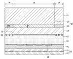
이하 도 2를 참조하여, 제 1 실시예에 따른 터치 윈도우의 커버 기판(100), 기판(110), 제 2 기판(120), 감지 전극(200), 배선 전극(300) 및 중간층(400)을 설명한다.2, the
상기 커버 기판(100)에는 유효 영역(AA) 및 비유효 영역(UA)이 정의될 수 있다. In the
상기 유효 영역(AA)에서는 디스플레이가 표시될 수 있고, 상기 유효 영역(AA) 주위에 배치되는 상기 비유효 영역(UA)에서는 디스플레이가 표시되지 않을 수 있다.The display may be displayed in the effective area AA and the display may not be displayed in the non-valid area UA disposed around the valid area AA.
또한, 상기 유효 영역(AA) 및 상기 비유효 영역(UA) 중 적어도 하나의 영역에서는 입력 장치(예를 들어, 손가락, 스타일러스 펜 등)의 위치를 감지할 수 있다. 이와 같은 터치 윈도우에 손가락 등의 입력 장치가 접촉되면, 입력 장치가 접촉된 부분에서 정전 용량의 차이가 발생하고, 이러한 차이가 발생한 부분을 접촉 위치로 검출할 수 있다.Also, at least one of the effective area AA and the ineffective area UA may sense the position of an input device (e.g., a finger, a stylus pen, etc.). When an input device such as a finger is brought into contact with such a touch window, a capacitance difference occurs at a portion where the input device is contacted, and a portion where such a difference occurs can be detected as the contact position.
상기 커버 기판(100) 상에는 별도의 기판(110)이 더 배치될 수 있다. 상기 커버 기판(100)과 상기 기판(110) 사이에는 중간층(400)이 배치될 수 있다. 상기 중간층(400)은 상기 커버 기판(100)의 유효 영역 및 비유효 영역 상에 배치됨에 따라, 상기 커버 기판(100)과 상기 기판(110)을 접착할 수 있다.A
상기 중간층(400)은 접착 물질을 포함할 수 있다. 상기 중간층(400)은 광학용 투명 접착제(OCA, OCR)를 포함할 수 있다. The
상기 중간층(400)의 일면은 상기 커버 기판(100)과 직접 접촉하고, 상기 중간층(400)의 상기 일면과 반대되는 타면은 상기 기판(110)과 직접 접촉할 수 있다.One side of the
상기 중간층(400)은 상기 커버 기판(100)의 유효 영역 상에 배치되는 제 1 중간층(410) 및 상기 커버 기판(100)의 비유효 영역 상에 배치되는 제 2 중간층(420)을 포함할 수 있다.The
상기 제 1 중간층(410)은 상기 제 2 중간층(420)과 상기 커버 기판(100)의 동일한 일면 상에 배치될 수 있다. The first
상기 제 1 중간층(410)의 측면은 상기 제 2 중간층(420)의 측면과 접촉하며 배치될 수 있다.The side surface of the first
상기 중간층(400)은 단일층일 수 있다. 즉, 상기 제 1 중간층(410) 및 상기 제 2 중간층(420)은 일체로 형성되는 단일층일 수 있다.The
예를 들어, 상기 기판(110) 상에 접착 물질을 도포할 수 있다. 다음으로, 상기 유효 영역과 대응되는 영역 상에 마스크를 배치할 수 있다. 다음으로, 상기 마스크가 배치되지 않은 비유효 영역 상에 블랙 잉크를 도포하고, 건조시킬 수 있다. 그 다음으로, 비유효 영역 상에 배치되는 접착 물질에 다시 블랙 잉크를 도포하고, 건조시킬 수 있다. For example, an adhesive material may be applied on the
유효 영역 상에 마스크를 배치한 후에 비유효 영역 상에 블랙 잉크를 도포함에 따라, 제 2 중간층(420)은 선택적으로 색을 가질 수 있다. 또한, 두 번의 블랙 잉크 도포과정에 의하여 상기 제 2 중간층(420)은 배선 전극이 시인되는 것을 방지할 수 있다. As the black ink is applied onto the ineffective area after the mask is placed on the effective area, the second
상기 제 1 중간층(410)은 투명한 물질을 포함할 수 있다. 예를 들어, 상기 제 1 중간층(410)은 아크릴계, 실리콘계, 우레탄계 고분자를 포함할 수 있다. 이에 따라, 상기 제 1 중간층(410)은 소재 자체의 투과도가 90%이상일 수 있어, 광투과율을 비롯한 광특성이 우수할 수 있다.The first
상기 제 1 중간층(410)은 광(UV)에 의하여 경화될 수 있는 광경화성 물질을 포함할 수 있다. 예를 들어, 상기 제 1 중간층(410)은 아크릴계 고분자를 포함할 수 있다. 이에 따라, 상기 제 1 중간층(410)은 빠른 경화 속도를 가지므로 공정 효율을 향상시킬 수 있다. The first
상기 제 2 중간층(420)은 색을 가질 수 있다. 상기 제 2 중간층(420)은 상기 제 1 중간층(410)과 대응되는 물질을 포함하고, 안료를 더 포함할 수 있다. The second
상기 제 2 중간층(420)은 아크릴계, 실리콘계, 우레탄계 고분자를 포함할 수 있다. 예를 들어, 상기 제 2 중간층(420)은 아크릴계 고분자를 포함하고, 안료를 더 포함할 수 있다. 자세하게, 상기 제 2 중간층(420)은 유기안료 및 무기안료 중 적어도 하나를 포함할 수 있다. 예를 들어, 상기 제 2 중간층(420)은 무기 안료로, 카본 블랙을 포함할 수 있다. 이에 따라, 상기 제 2 중간층(420)은 블랙 색을 가질 수 있다. 상기 제 2 중간층(420)은 색을 가질 수 있음에 따라, 배선 전극이나 회로 기판이 시인되는 것을 방지할 수 있다. The second
즉, 실시예에 따른 터치 윈도우는 상기 커버 기판(100) 상에 상기 제 2 중간층(420)이 배치됨에 따라, 데코층 또는 데코필름을 생략할 수 있다.That is, in the touch window according to the embodiment, since the second
이에 따라, 실시예에 따른 터치 윈도우는 데코층의 단차에 의하여 기판의 경계가 시인될 수 있는 문제점을 방지할 수 있으므로, 시인성이 향상된 터치 윈도우를 제공할 수 있다. Accordingly, the touch window according to the embodiment can prevent the problem that the boundary of the substrate can be visually recognized by the step of the decor layer, so that a touch window with improved visibility can be provided.
상기 중간층(400)은 유효 영역과 비유효 영역 상에 일정한 두께로 배치될 수 있다. 자세하게, 상기 제 1 중간층(410)의 두께(T1)는 상기 제 2 중간층(420)의 두께(T2)와 대응될 수 있다. 예를 들어, 상기 제 1 중간층(410)의 두께(T1) 및 상기 제 2 중간층(420)의 두께(T2)는 50㎛이하일 수 있다. 예를 들어, 상기 제 1 중간층(410)의 두께(T1) 및 상기 제 2 중간층(420)의 두께(T2)는 35㎛이하일 수 있다. 예를 들어, 상기 제 1 중간층(410)의 두께(T1) 및 상기 제 2 중간층(420)의 두께(T2)는 15㎛ 내지 30㎛일 수 있다.The
상기 제 1 중간층(410)의 두께(T1) 및 상기 제 2 중간층(420)의 두께(T2)가 15㎛ 미만인 경우에는 중간층의 접착력 저하에 의에 의한 박리가 발생할 수 있고, 이에 따라, 터치 윈도우의 신뢰성이 저하될 수 있다. If the thickness T1 of the first
상기 제 1 중간층(410)의 두께(T1) 및 상기 제 2 중간층(420)의 두께(T2)가 50㎛ 초과인 경우에는 터치 윈도우의 두께가 증가할 수 있다.If the thickness T1 of the first
상기 제 1 중간층(410)의 상면의 높이는 상기 제 2 중간층(420)의 상면의 높이와 대응될 수 있다. 즉, 상기 제 1 중간층(410)의 상면은 상기 제 2 중간층(420)의 상면과 연결되어, 평면을 형성할 수 있다. 예를 들어, 상기 제 1 중간층(410) 및 상기 제 2 중간층(420)의 상면은 상기 기판(110)의 상면과 마주보며 배치될 수 있다. The height of the upper surface of the first
즉, 실시예에 따른 터치 윈도우는 비유효 영역에서 데코층을 생략할 수 있으므로, 데코층 상에 접착층이 배치됨에 따라 발생할 수 있는 접착층의 배치 불량 또는 접착층의 기포로 인한 불량을 방지할 수 있다. 이에 따라, 신뢰성 및 공정 효율이 향상된 터치 윈도우를 제공할 수 있다.That is, since the touch window according to the embodiment can omit the decor layer in the ineffective area, it is possible to prevent defective placement due to defective placement of the adhesive layer or bubble of the adhesive layer that may occur as the adhesive layer is disposed on the decor layer. Accordingly, a touch window with improved reliability and process efficiency can be provided.
또한, 실시예에 따른 터치 윈도우는 비유효 영역에서 상기 데코층의 두께만큼 터치 윈도우의 두께가 얇아질 수 있으므로, 실시예에 따른 터치 윈도우는 슬림한 두께의 터치 윈도우를 제공할 수 있다.The touch window according to the embodiment can provide a touch window having a slim thickness because the thickness of the touch window can be reduced by the thickness of the decor layer in the ineffective area.
또한, 실시예에 따른 터치 윈도우는 데코층 또는 데코필름의 배치 공정을 생략할 수 있어, 공정 비용을 저감시킬 수 있고, 공정 효율이 향상될 수 있다. Further, in the touch window according to the embodiment, the step of arranging the decor layer or the deco film can be omitted, the process cost can be reduced, and the process efficiency can be improved.
또한, 상기 기판(110) 상에는 별도의 제 2 기판(120)이 더 배치될 수 있다. 상기 기판(110)과 상기 제 2 기판(120) 사이에는 제 3 중간층(430)이 배치될 수 있다. 상기 제 3 중간층(430)은 상기 기판(110)의 유효 영역 및 비유효 영역 상에 배치됨에 따라, 상기 기판(110)과 상기 제 2 기판(120)을 접착할 수 있다.A separate
상기 제 3 중간층(430)의 일면은 상기 기판(110)과 직접 접촉하고, 상기 중간층(400)의 일면과 반대되는 타면은 상기 제 2 기판(120)과 직접 접촉할 수 있다.One surface of the third
상기 제 3 중간층(430)은 접착 물질을 포함할 수 있다. 상기 제 3 중간층(430)은 광학용 투명 접착제(OCA, OCR)를 포함할 수 있다.The third
상기 제 3 중간층(430)은 단일층일 수 있다. 상기 제 3 중간층(430)은 투명한 물질을 포함할 수 있다. 상기 제 3 중간층(430)은 제 1 중간층(410)과 대응되는 물질을 포함할 수 있다. 예를 들어, 상기 제 3 중간층(430)은 아크릴계 고분자를 포함할 수 있다. 이에 따라, 상기 제 3 중간층(430)은 광투과율을 비롯한 광특성이 우수할 수 있다.The third
상기 감지 전극(200) 및 상기 배선 전극(300)은 상기 기판(110)과 상기 제 2 기판(120)에 의해 지지되고, 상기 기판(110)과 상기 커버 기판(100)은 상기 제 1 중간층(410) 및 상기 제 2 중간층(420)을 통해 집적 또는 간접적으로 접착될 수 있고, 상기 기판(110)과 상기 제 2 기판(120)은 제 3 중간층(430)을 통해 직접 또는 간접적으로 접착될 수 있다. 이에 따라, 커버기판과 기판을 각각 따로 형성할 수 있으므로, 터치윈도우 대량생산에 유리 할 수 있다.The
상기 감지 전극(200)은 상기 기판(110) 상에 배치될 수 있다. 예를 들어, 상기 감지 전극(200)은 상기 기판(110)의 유효 영역(AA) 상에 배치될 수 있다.The
상기 배선 전극(300)은 상기 기판(110) 상에 배치될 수 있다. 자세하게, 상기 배선 전극(300)은 상기 기판(110)의 유효 영역(AA) 및 비유효 영역(UA) 중 적어도 하나의 영역 상에 배치될 수 있다. 바람직하게는, 상기 배선 전극(300)은 상기 기판(110)의 상기 비유효 영역(UA) 상에 배치될 수 있다.The
상기 기판(110) 상에는 상기 제 1 감지 전극(210) 및 상기 제 1 배선 전극(310)이 배치될 수 있다. 예를 들어, 상기 제 1 감지 전극(210) 및 상기 제 1 배선 전극(310)은 상기 기판(110)의 일면 상에 직접 배치될 수 있다. The
상기 제 2 기판(120) 상에는 상기 제 2 감지 전극(220) 및 상기 제 2 배선 전극(320)이 배치될 수 있다. 예를 들어, 상기 제 2 감지 전극(220) 및 상기 제 2 배선 전극(320)은 상기 2 기판(120)의 일면 상에 직접 배치될 수 있다. The
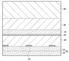
도 3 및 도 4는 제 2 실시예에 따른 터치 윈도우에 관한 것이다. 상기 제 1 실시예와 중복되는 설명은 생략될 수 있다. 동일한 구성에 대해서는 동일한 도면 부호를 부여한다.Figs. 3 and 4 relate to a touch window according to the second embodiment. Fig. The description overlapping with the first embodiment may be omitted. The same reference numerals are assigned to the same components.
이하, 도 3 및 도 4는 제 2 실시예에 따른 터치 윈도우의 커버 기판(100), 기판(110), 감지 전극(200), 배선 전극(300) 및 중간층(400)을 설명한다.3 and 4 illustrate the
실시예에 따른 터치 윈도우는 상기 커버 기판(100) 및 상기 기판(110)을 포함하고, 상기 기판(110) 상의 제 1 감지 전극(210) 및 제 2 감지 전극(220)을 포함할 수 있다.The touch window according to the embodiment may include the
자세하게, 상기 기판(110)의 일면에는 일 방향으로 연장하는 상기 제 1 감지 전극(210) 및 상기 제 1 감지 전극(210)과 연결되는 제 1 배선 전극(310)이 배치되고, 상기 기판(110)의 상기 일면과 대응되는 일면 상에는 상기 일 방향과 다른 방향으로 연장하는 제 2 감지 전극(220) 및 상기 제 2 감지 전극(220)과 연결되는 제 2 배선 전극(320)이 배치될 수 있다.The
즉, 상기 제 1 감지 전극(210)과 상기 제 2 감지 전극(220)은 상기 기판(110)의 동일 면 상에서 서로 다른 방향으로 연장되며 배치될 수 있다.That is, the
상기 제 1 감지 전극(210)과 상기 제 2 감지 전극(220)은 상기 기판(110) 상에서 서로 절연되며 배치될 수 있다. 자세하게, 상기 제 1 감지 전극(210)을 구성하는 복수 개의 제 1 단위 감지 전극들은 서로 연결되며 배치되고, 상기 제 2 감지 전극(220)을 구성하는 복수 개의 제 2 단위 감지 전극들은 서로 이격되며 배치될 수 있다. 상기 제 2 단위 감지 전극들은 브리지 전극(230)에 의해 연결되고, 상기 브리지 전극(230)이 배치되는 부분에 절연 물질(250)을 배치하여, 상기 제 1 감지 전극(210)과 상기 제 2 감지 전극(220)은 서로 단락시킬 수 있다.The
이에 따라, 상기 제 1 감지 전극(210)과 상기 제 2 감지 전극(220)은 서로 접촉되지 않고, 상기 기판(110)의 동일한 일면 즉, 유효 영역(AA)의 동일 면 상에서 서로 절연되며 배치될 수 있다. Accordingly, the
또한, 상기 제 1 감지 전극(210) 및 상기 제 2 감지 전극(220) 중 적어도 하나의 감지 전극은 메쉬 형상으로 배치될 수 있다.Also, at least one of the
상기 커버 기판(100) 상에는 상기 기판(110)이 배치되고, 상기 커버 기판(100)과 상기 기판(110)은 중간층(400)을 통해 서로 접착될 수 있다.The
즉, 상기 제 1 실시예와 달리, 상기 기판(110)의 일면 상에 상기 제 1 감지 전극(210), 상기 제 2 감지 전극(220), 상기 제 1 배선 전극(310) 및 상기 제 2 배선 전극(320)이 모두 배치될 수 있어, 상기 제 1 실시예에 따른 상기 제 2 기판(120)을 생략함에 따라, 터치 윈도우의 두께가 더 감소될 수 있다. That is, unlike the first embodiment, the
도 4를 참조하면, 상기 커버 기판(100) 상에 상기 기판(110)이 배치될 수 있다. 상기 커버 기판(100)과 상기 기판(110) 사이에는 중간층(400)이 배치될 수 있다. 상기 중간층(400)은 상기 커버 기판(100)의 유효 영역 및 비유효 영역 상에 배치됨에 따라, 상기 커버 기판(100)과 상기 기판(110)을 접착할 수 있다. Referring to FIG. 4, the
상기 중간층(400)은 접착 물질을 포함할 수 있다. 상기 중간층(400)은 광학용 투명 접착제(OCA, OCR)를 포함할 수 있다. The
상기 중간층(400)의 일면은 상기 커버 기판(100)과 직접 접촉하고, 상기 중간층(400)의 상기 일면과 반대되는 타면은 상기 기판(110)과 직접 접촉할 수 있다.One side of the
상기 중간층(400)은 상기 커버 기판(100)의 유효 영역 상에 배치되는 제 1 중간층(410) 및 상기 커버 기판(100)의 비유효 영역 상에 배치되는 제 2 중간층(420)을 포함할 수 있다.The
상기 제 1 중간층(410)은 상기 제 2 중간층(420)과 상기 커버 기판(100)의 동일한 일면 상에 배치될 수 있다. The first
상기 제 1 중간층(410)의 측면은 상기 제 2 중간층(420)의 측면과 접촉하며 배치될 수 있다.The side surface of the first
상기 중간층(400)은 단일층일 수 있다. 즉, 상기 제 1 중간층(410) 및 상기 제 2 중간층(420)은 일체로 형성되는 단일층일 수 있다.The
상기 제 1 중간층(410)은 투명한 물질을 포함할 수 있다. 예를 들어, 상기 제 1 중간층(410)은 아크릴계, 실리콘계, 우레탄계 고분자를 포함할 수 있다. 이에 따라, 상기 제 1 중간층(410)은 소재 자체의 투과도가 90%이상일 수 있어, 광투과율을 비롯한 광특성이 우수할 수 있다.The first
상기 제 1 중간층(410)은 광(UV)에 의하여 경화될 수 있는 광경화성 물질을 포함할 수 있다. 예를 들어, 상기 제 1 중간층(410)은 아크릴계 고분자를 포함할 수 있다. 이에 따라, 상기 제 1 중간층(410)은 빠른 경화 속도를 가지므로 공정 효율을 향상시킬 수 있다. The first
상기 제 2 중간층(420)은 색을 가질 수 있다. 상기 제 2 중간층(420)은 상기 제 1 중간층(410)과 대응되는 물질을 포함하고, 안료를 더 포함할 수 있다. The second
상기 제 2 중간층(420)은 아크릴계, 실리콘계, 우레탄계 고분자를 포함할 수 있다. 예를 들어, 상기 제 2 중간층(420)은 아크릴계 고분자를 포함하고, 안료를 더 포함할 수 있다. 자세하게, 상기 제 2 중간층(420)은 유기안료 및 무기안료 중 적어도 하나를 포함할 수 있다. 예를 들어, 상기 제 2 중간층(420)은 무기 안료로, 카본 블랙을 포함할 수 있다. 이에 따라, 상기 제 2 중간층(420)은 블랙 색을 가질 수 있다. 상기 제 2 중간층(420)은 색을 가질 수 있음에 따라, 배선 전극이나 회로 기판이 시인되는 것을 방지할 수 있다. The second
즉, 실시예에 따른 터치 윈도우는 상기 커버 기판(100) 상에 상기 제 2 중간층(420)이 배치됨에 따라, 데코층 또는 데코필름을 생략할 수 있다.That is, in the touch window according to the embodiment, since the second
이에 따라, 실시예에 따른 터치 윈도우는 데코층의 단차에 의하여 기판의 경계가 시인될 수 있는 문제점을 방지할 수 있으므로, 시인성이 향상된 터치 윈도우를 제공할 수 있다. Accordingly, the touch window according to the embodiment can prevent the problem that the boundary of the substrate can be visually recognized by the step of the decor layer, so that a touch window with improved visibility can be provided.
상기 중간층(400)은 유효 영역과 비유효 영역 상에 일정한 두께로 배치될 수 있다. 자세하게, 상기 제 1 중간층(410)의 두께(T1)는 상기 제 2 중간층(420)의 두께(T2)와 대응될 수 있다. 예를 들어, 상기 제 1 중간층(410)의 두께(T1) 및 상기 제 2 중간층(420)의 두께(T2)는 50㎛이하일 수 있다. 예를 들어, 상기 제 1 중간층(410)의 두께(T1) 및 상기 제 2 중간층(420)의 두께(T2)는 35㎛이하일 수 있다. 예를 들어, 상기 제 1 중간층(410)의 두께(T1) 및 상기 제 2 중간층(420)의 두께(T2)는 15㎛ 내지 30㎛일 수 있다.The
상기 제 1 중간층(410)의 두께(T1) 및 상기 제 2 중간층(420)의 두께(T2)가 15㎛ 미만인 경우에는 중간층의 접착력 저하에 의에 의한 박리가 발생할 수 있고, 이에 따라, 터치 윈도우의 신뢰성이 저하될 수 있다. If the thickness T1 of the first
상기 제 1 중간층(410)의 두께(T1) 및 상기 제 2 중간층(420)의 두께(T2)가 50㎛ 초과인 경우에는 터치 윈도우의 두께가 증가할 수 있다.If the thickness T1 of the first
상기 제 1 중간층(410)의 상면의 높이는 상기 제 2 중간층(420)의 상면의 높이와 대응될 수 있다. 즉, 상기 제 1 중간층(410)의 상면은 상기 제 2 중간층(420)의 상면과 연결되어, 평면을 형성할 수 있다. 예를 들어, 상기 제 1 중간층(410) 및 상기 제 2 중간층(420)의 상면은 상기 기판(110)의 상면과 마주보며 평행하게 배치될 수 있다. The height of the upper surface of the first
즉, 실시예에 따른 터치 윈도우는 비유효 영역에서 데코층을 생략할 수 있으므로, 데코층 상에 접착층이 배치됨에 따라 발생할 수 있는 접착층의 배치 불량 또는 접착층의 기포로 인한 불량을 방지할 수 있다. 이에 따라, 신뢰성 및 공정 효율이 향상된 터치 윈도우를 제공할 수 있다.That is, since the touch window according to the embodiment can omit the decor layer in the ineffective area, it is possible to prevent defective placement due to defective placement of the adhesive layer or bubble of the adhesive layer that may occur as the adhesive layer is disposed on the decor layer. Accordingly, a touch window with improved reliability and process efficiency can be provided.
또한, 실시예에 따른 터치 윈도우는 비유효 영역에서 상기 데코층의 두께만큼 터치 윈도우의 두께가 얇아질 수 있으므로, 실시예에 따른 터치 윈도우는 슬림한 두께의 터치 윈도우를 제공할 수 있다.The touch window according to the embodiment can provide a touch window having a slim thickness because the thickness of the touch window can be reduced by the thickness of the decor layer in the ineffective area.
또한, 실시예에 따른 터치 윈도우는 데코층 또는 데코필름의 배치 공정을 생략할 수 있어, 공정 비용을 저감시킬 수 있고, 공정 효율이 향상될 수 있다. Further, in the touch window according to the embodiment, the step of arranging the decor layer or the deco film can be omitted, the process cost can be reduced, and the process efficiency can be improved.
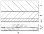
앞서 설명한 터치 윈도우는 표시 패널과 결합하여 터치 디바이스에 적용될 수 있다. 예를 들어, 터치 윈도우는 표시 패널과 접착층에 의해 결합될 수 있다.The touch window described above can be applied to a touch device in combination with a display panel. For example, the touch window may be coupled to the display panel by an adhesive layer.
도 5를 참조하면, 실시예에 따른 터치 디바이스는 표시 패널(500) 상에 배치되는 터치 윈도우를 포함할 수 있다.Referring to FIG. 5, the touch device according to the embodiment may include a touch window disposed on the
자세하게, 도 5를 참조하면, 상기 터치 디바이스는 상기 기판(110)과 상기 표시 패널(500)이 결합되어 형성될 수 있다. 상기 기판(110)과 상기 표시 패널(500)은 제 4 중간층(440)을 통해 서로 접착될 수 있다. 예를 들어, 상기 기판(110)과 상기 표시 패널(500)은 광학용 투명 접착제(OCA, OCR)를 포함하는 제 4 중간층(440)을 통해 서로 합지될 수 있다.5, the touch device may be formed by combining the
상기 표시 패널(500)은 제 1' 기판(510) 및 제 2' 기판(520)을 포함할 수 있다.The
상기 표시 패널(500)이 액정표시패널인 경우, 상기 표시 패널(500)은 박막트랜지스터(Thin Film Transistor,TFT)와 화소전극을 포함하는 제 1' 기판(510)과 컬러필터층들을 포함하는 제 2' 기판(520)이 액정층을 사이에 두고 합착된 구조로 형성될 수 있다. When the
또한, 상기 표시 패널(500)은 박막트랜지스터, 칼라필터 및 블랙매트릭스가 제 1' 기판(510)에 형성되고, 제 2' 기판(520)이 액정층을 사이에 두고 상기 제 1' 기판(510)과 합착되는 COT(color filter on transistor)구조의 액정표시패널일 수도 있다. 즉, 상기 제 1' 기판(510) 상에 박막 트랜지스터를 형성하고, 상기 박막 트랜지스터 상에 보호막을 형성하고, 상기 보호막 상에 컬러필터층을 형성할 수 있다. 또한, 상기 제 1' 기판(510)에는 상기 박막 트랜지스터와 접촉하는 화소전극을 형성한다. 이때, 개구율을 향상하고 마스크 공정을 단순화하기 위해 블랙매트릭스를 생략하고, 공통 전극이 블랙매트릭스의 역할을 겸하도록 형성할 수도 있다.In addition, the
또한, 상기 표시 패널(500)이 액정표시패널인 경우, 상기 표시 장치는 상기 표시 패널(500) 배면에서 광을 제공하는 백라이트 유닛을 더 포함할 수 있다. When the
상기 표시 패널(500)이 유기전계발광표시패널인 경우, 상기 표시 패널(500)은 별도의 광원이 필요하지 않은 자발광 소자를 포함한다. 상기 표시 패널(500)은 제 1' 기판(510) 상에 박막트랜지스터가 형성되고, 상기 박막트랜지스터와 접촉하는 유기발광소자가 형성된다. 상기 유기발광소자는 양극, 음극 및 상기 양극과 음극 사이에 형성된 유기발광층을 포함할 수 있다. 또한, 상기 유기발광소자 상에 인캡슐레이션을 위한 봉지 기판 역할을 하는 제 2' 기판(520)을 더 포함할 수 있다.When the
도 6을 참조하면, 실시예에 따른 터치 디바이스는 표시 패널(500)과 일체로 형성된 터치 윈도우를 포함할 수 있다. 즉, 적어도 하나의 감지 전극을 지지하는 기판이 생략될 수 있다.Referring to FIG. 6, the touch device according to the embodiment may include a touch window formed integrally with the
자세하게는, 상기 표시 패널(500)의 적어도 일면에 적어도 하나의 감지 전극이 배치될 수 있다. 즉, 상기 제 1' 기판(510) 또는 상기 제 2' 기판(520)의 적어도 일면에 적어도 하나의 감지 전극이 형성될 수 있다.In detail, at least one sensing electrode may be disposed on at least one surface of the
이때, 상부에 배치된 기판의 상면에 적어도 하나의 감지 전극이 형성될 수 있다. At this time, at least one sensing electrode may be formed on the upper surface of the substrate disposed above.
도 6을 참조하면, 상기 기판(110)의 일면에 제 1 감지 전극(210)이 배치될 수 있다. 또한, 상기 제 1 감지 전극(210)과 연결되는 제 1 배선이 배치될 수 있다. 또한, 상기 표시 패널(500)의 일면에 제 2 감지 전극(220)이 배치될 수 있다. 또한, 상기 제 2 감지 전극(220)과 연결되는 제 2 배선이 배치될 수 있다. Referring to FIG. 6, the
상기 기판(110)과 상기 표시 패널(500) 사이에는 상기 제 4 중간층(440)이 배치되어, 상기 기판과 상기 표시 패널(500)은 서로 합지될 수 있다. The fourth
또한, 상기 기판(110) 하부에 편광판을 더 포함할 수 있다. 상기 편광판은 선 편광판 또는 외광 반사 방지 편광판 일 수 있다. 예를 들면, 상기 표시 패널(500)이 액정표시패널인 경우, 상기 편광판은 선 편광판일 수 있다. 또한, 상기 표시 패널(500)이 유기전계발광표시패널인 경우, 상기 편광판은 외광 반사 방지 편광판 일 수 있다. In addition, a polarizing plate may be further disposed under the
실시예에 따른 터치 디바이스는 감지 전극을 지지하는 적어도 하나의 기판을 생략할 수 있다. 이로 인해, 두께가 얇고 가벼운 터치 디바이스를 형성할 수 있다.The touch device according to the embodiment may omit at least one substrate supporting the sensing electrode. As a result, a touch device with a thin thickness and light weight can be formed.
도 7을 참조하면, 실시예에 따른 터치 디바이스는 표시 패널(500)과 일체로 형성된 터치 윈도우를 포함할 수 있다. 즉, 적어도 하나의 감지 전극을 지지하는 기판이 생략될 수 있다.Referring to FIG. 7, the touch device according to the embodiment may include a touch window formed integrally with the
예를 들어, 유효 영역에 배치되어 터치를 감지하는 센서 역할을 하는 감지 전극과 상기 감지 전극으로 전기적 신호를 인가하는 배선이 상기 표시 패널의 내측에 형성될 수 있다. 자세하게, 적어도 하나의 감지 전극 또는 적어도 하나의 배선이 상기 표시 패널의 내측에 형성될 수 있다. For example, a sensing electrode serving as a sensor for sensing a touch disposed in the effective area and a wiring for applying an electrical signal to the sensing electrode may be formed on the inner side of the display panel. In detail, at least one sensing electrode or at least one wiring may be formed inside the display panel.
상기 표시 패널은 제 1' 기판(510) 및 제 2' 기판(520)을 포함한다. 이때, 상기 제 1' 기판(510) 및 제 2' 기판(520)의 사이에 제 1 감지 전극(210) 및 제 2 감지 전극(220) 중 적어도 하나의 감지 전극이 배치된다. 즉, 상기 제 1' 기판(510) 또는 상기 제 2' 기판(520)의 적어도 일면에 적어도 하나의 감지 전극이 배치될 수 있다.The display panel includes a
도 7을 참조하면, 상기 기판(110)의 일면에 제 1 감지 전극(210)이 배치될 수 있다. 또한, 상기 제 1 감지 전극(210)과 연결되는 제 1 배선이 배치될 수 있다. 또한, 상기 제 1' 기판(510) 및 제 2' 기판(520) 사이에 제 2 감지 전극(220) 및 제 2 배선이 형성될 수 있다. 즉, 표시 패널의 내측에 제 2 감지 전극(220) 및 제 2 배선이 배치되고, 표시 패널의 외측에 제 1 감지 전극(210) 및 제 1 배선이 배치될 수 있다.Referring to FIG. 7, a
상기 제 2 감지 전극(220) 및 제 2 배선은 상기 제 1' 기판(510)의 상면 또는 상기 제 2' 기판(520)의 배면에 배치될 수 있다. The
또한, 상기 기판(110) 하부에 편광판을 더 포함할 수 있다.In addition, a polarizing plate may be further disposed under the
상기 표시 패널이 액정표시패널인 경우, 상기 제 2 감지 전극이 제 1' 기판(510) 상면에 형성되는 경우, 상기 감지 전극은 박막트랜지스터(Thin Film Transistor,TFT) 또는 화소전극과 함께 형성될 수 있다. 또한, 상기 제 2 감지 전극이 제 2' 기판(520) 배면에 형성되는 경우, 상기 감지 전극 상에 컬러필터층이 형성되거나, 상기 컬러필터층 상에 감지 전극이 형성될 수 있다. 상기 표시 패널이 유기전계발광표시패널인 경우, 상기 제 2 감지 전극이 제 1' 기판(510)의 상면에 형성되는 경우, 상기 제 2 감지 전극은 박막트랜지스터 또는 유기발광소자와 함께 형성될 수 있다. When the display panel is a liquid crystal display panel, when the second sensing electrode is formed on the upper surface of the
실시예에 따른 터치 디바이스는 감지 전극을 지지하는 적어도 하나의 기판을 생략할 수 있다. 이로 인해, 두께가 얇고 가벼운 터치 디바이스를 형성할 수 있다. 또한, 표시 패널에 형성되는 소자와 함께 감지 전극 및 배선을 형성하여 공정을 단순화 하고, 비용을 절감할 수 있다.The touch device according to the embodiment may omit at least one substrate supporting the sensing electrode. As a result, a touch device with a thin thickness and light weight can be formed. Further, the sensing electrode and the wiring are formed together with the element formed on the display panel, thereby simplifying the process and reducing the cost.
이하, 도 8 내지 도 11를 참조하여, 앞서 설명한 실시예들에 따른 터치 윈도우가 적용되는 디스플레이 장치의 일례를 설명한다.Hereinafter, an example of a display device to which a touch window according to the above-described embodiments is applied will be described with reference to FIGS. 8 to 11. FIG.
도 8을 참고하면, 터치 디바이스 장치의 일례로서, 이동식 단말기가 도시되어 있다. 상기 이동식 단말기는 유효 영역(AA) 및 비유효 영역(UA)을 포함할 수 있다. 상기 유효 영역(AA)은 손가락 등의 터치에 의해 터치 신호를 감지하고, 상기 비유효 영역에는 명령 아이콘 패턴부 및 로고 등이 형성될 수 있다.Referring to Fig. 8, a mobile terminal is shown as an example of a touch device. The mobile terminal may include a valid area AA and a non-valid area UA. The effective area AA senses a touch signal by touching a finger or the like, and a command icon pattern part and a logo are formed on the non-valid area.
도 9를 참조하면, 이러한 터치 윈도우는 이동식 단말기 등의 터치 디바이스 장치뿐만 아니라 자동차 네비게이션에도 적용될 수 있다.Referring to FIG. 9, such a touch window can be applied not only to a touch device such as a mobile terminal but also to a car navigation system.
도 10을 참조하면, 터치 윈도우는 휘어지는 플렉서블(flexible) 터치 윈도우를 포함할 수 있다. 따라서, 이를 포함하는 터치 디바이스 장치는 플렉서블 터치 디바이스 장치일 수 있다. 따라서, 사용자가 손으로 휘거나 구부릴 수 있다. 이러한 플렉서블 터치 윈도우는 웨어러블 터치 등에 적용될 수 있다.Referring to FIG. 10, the touch window may include a flexible flexible touch window. Accordingly, the touch device device including the same may be a flexible touch device device. Therefore, the user can bend or bend by hand. Such a flexible touch window can be applied to a wearable touch or the like.
또한, 도 11을 참조하면, 이러한 터치 윈도우는 차량 내에도 적용될 수 있다. 즉, 상기 터치 윈도우는 차량 내에서 터치 윈도우가 적용될 수 있는 다양한 부분에 적용될 수 있다. 따라서, PND(Personal Navigation Display)뿐만 아니라, 계기판(dashboard) 등에 적용되어 CID(Center Information Display)도 구현할 수 있다. 그러나, 실시예가 이에 한정되는 것은 아니고, 이러한 터치 디바이스 장치는 다양한 전자 제품에 사용될 수 있음은 물론이다.11, such a touch window can also be applied to a vehicle. That is, the touch window can be applied to various parts to which a touch window can be applied in the vehicle. Therefore, not only PND (Personal Navigation Display) but also dashboard can be applied to implement CID (Center Information Display). However, the embodiment is not limited thereto, and it goes without saying that such a touch device device can be used for various electronic products.
상술한 실시예에 설명된 특징, 구조, 효과 등은 본 발명의 적어도 하나의 실시예에 포함되며, 반드시 하나의 실시예에만 한정되는 것은 아니다. 나아가, 각 실시예에서 예시된 특징, 구조, 효과 등은 실시예들이 속하는 분야의 통상의 지식을 가지는 자에 의하여 다른 실시예들에 대해서도 조합 또는 변형되어 실시 가능하다. 따라서 이러한 조합과 변형에 관계된 내용들은 본 발명의 범위에 포함되는 것으로 해석되어야 할 것이다. The features, structures, effects and the like described in the foregoing embodiments are included in at least one embodiment of the present invention and are not necessarily limited to one embodiment. Further, the features, structures, effects, and the like illustrated in the embodiments may be combined or modified in other embodiments by those skilled in the art to which the embodiments belong. Therefore, it should be understood that the present invention is not limited to these combinations and modifications.
또한, 이상에서 실시예들을 중심으로 설명하였으나 이는 단지 예시일 뿐 본 발명을 한정하는 것이 아니며, 본 발명이 속하는 분야의 통상의 지식을 가진 자라면 본 실시예의 본질적인 특성을 벗어나지 않는 범위에서 이상에 예시되지 않은 여러 가지의 변형과 응용이 가능함을 알 수 있을 것이다. 예를 들어, 실시예들에 구체적으로 나타난 각 구성 요소는 변형하여 실시할 수 있는 것이다. 그리고 이러한 변형과 응용에 관계된 차이점들은 첨부한 청구 범위에서 규정하는 본 발명의 범위에 포함되는 것으로 해석되어야 할 것이다.While the present invention has been particularly shown and described with reference to exemplary embodiments thereof, it is clearly understood that the same is by way of illustration and example only and is not to be construed as limiting the scope of the present invention. It can be seen that various modifications and applications are possible. For example, each component specifically shown in the embodiments may be modified and implemented. It is to be understood that the present invention may be embodied in many other specific forms without departing from the spirit or essential characteristics thereof.
Claims (10)
상기 커버 기판 상에 배치되는 중간층;
상기 중간층 상에 배치되는 기판; 및
상기 기판 상에 배치되는 전극을 포함하는 터치 윈도우.A cover substrate including a valid region and a non-valid region;
An intermediate layer disposed on the cover substrate;
A substrate disposed on the intermediate layer; And
And an electrode disposed on the substrate.
상기 중간층은 상기 유효 영역 및 상기 비유효 영역 상에 배치되는 것을 포함하는 터치 윈도우.The method according to claim 1,
Wherein the intermediate layer is disposed on the valid region and the non-valid region.
상기 중간층은 단일층인 것을 포함하는 터치 윈도우.The method according to claim 1,
Wherein the intermediate layer is a single layer.
상기 유효 영역 상에 배치되는 상기 중간층은 투명한 물질인 것을 포함하는 터치 윈도우.The method according to claim 1,
Wherein the intermediate layer disposed on the effective region is a transparent material.
상기 비유효 영역 상에 배치되는 상기 중간층은 색을 가지는 것을 포함하는 터치 윈도우.The method according to claim 1,
Wherein the intermediate layer disposed on the ineffective area comprises a color.
상기 중간층은 접착 물질을 포함하는 터치 윈도우.The method according to claim 1,
Wherein the intermediate layer comprises an adhesive material.
상기 중간층의 두께는 50㎛이하 인 것을 포함하는 터치 윈도우.The method according to claim 1,
Wherein the intermediate layer has a thickness of 50 mu m or less.
상기 비유효 영역 상에 배치되는 상기 중간층은 유기안료 및 무기안료 중 적어도 하나를 포함하는 터치 윈도우.3. The method of claim 2,
Wherein the intermediate layer disposed on the ineffective area comprises at least one of an organic pigment and an inorganic pigment.
상기 유효 영역 상에 배치되는 상기 중간층의 상면의 높이는 상기 비유효 영역 상에 배치되는 상기 중간층의 상면의 높이와 대응되는 것을 포함하는 터치 윈도우.The method according to claim 1,
Wherein a height of an upper surface of the intermediate layer disposed on the effective area corresponds to a height of an upper surface of the intermediate layer disposed on the ineffective area.
상기 전극은 메쉬 형상인 것을 포함하는 터치 윈도우.The method according to claim 1,
Wherein the electrodes are mesh-shaped.
Priority Applications (1)
| Application Number | Priority Date | Filing Date | Title |
|---|---|---|---|
| KR1020160005983A KR20170086304A (en) | 2016-01-18 | 2016-01-18 | Touch window |
Applications Claiming Priority (1)
| Application Number | Priority Date | Filing Date | Title |
|---|---|---|---|
| KR1020160005983A KR20170086304A (en) | 2016-01-18 | 2016-01-18 | Touch window |
Publications (1)
| Publication Number | Publication Date |
|---|---|
| KR20170086304A true KR20170086304A (en) | 2017-07-26 |
Family
ID=59427184
Family Applications (1)
| Application Number | Title | Priority Date | Filing Date |
|---|---|---|---|
| KR1020160005983A KR20170086304A (en) | 2016-01-18 | 2016-01-18 | Touch window |
Country Status (1)
| Country | Link |
|---|---|
| KR (1) | KR20170086304A (en) |
-
2016
- 2016-01-18 KR KR1020160005983A patent/KR20170086304A/en not_active Application Discontinuation
Similar Documents
| Publication | Publication Date | Title |
|---|---|---|
| US10474305B2 (en) | Touch window | |
| US10078386B2 (en) | Touch device | |
| US9791981B2 (en) | Touch window and touch device including the same | |
| US9772727B2 (en) | Touch panel | |
| US9823792B2 (en) | Touch panel | |
| US10013084B2 (en) | Bendable touch window and touch device with the same | |
| US9619092B2 (en) | Touch panel | |
| US10318026B2 (en) | Touch window | |
| US10175800B2 (en) | Electrode member and touch window comprising the same | |
| KR20170084627A (en) | Touch window | |
| KR102029710B1 (en) | Touch panel | |
| KR20180113074A (en) | Touch panel | |
| KR20180113081A (en) | Touch panel | |
| KR20170093627A (en) | Touch window | |
| KR20170086304A (en) | Touch window | |
| KR20170129530A (en) | Touch window and touch device | |
| KR102302824B1 (en) | Touch window and touch device | |
| KR102313967B1 (en) | Touch window | |
| KR20170118475A (en) | Touch window and touch device | |
| KR20170001328A (en) | Touch window | |
| KR20170136758A (en) | Touch window and touch device | |
| KR20170046455A (en) | Touch window | |
| KR20170119868A (en) | Touch window | |
| KR20160070537A (en) | Touch window | |
| KR20170100374A (en) | Touch window and touch divice |
Legal Events
| Date | Code | Title | Description |
|---|---|---|---|
| A201 | Request for examination | ||
| E902 | Notification of reason for refusal | ||
| E601 | Decision to refuse application |