KR20170052760A - Display device and fabricating mehtod of the same - Google Patents
Display device and fabricating mehtod of the same Download PDFInfo
- Publication number
- KR20170052760A KR20170052760A KR1020150154074A KR20150154074A KR20170052760A KR 20170052760 A KR20170052760 A KR 20170052760A KR 1020150154074 A KR1020150154074 A KR 1020150154074A KR 20150154074 A KR20150154074 A KR 20150154074A KR 20170052760 A KR20170052760 A KR 20170052760A
- Authority
- KR
- South Korea
- Prior art keywords
- guide plate
- light guide
- adhesive tape
- chassis
- fastening
- Prior art date
Links
Images


Classifications
-
- G—PHYSICS
- G02—OPTICS
- G02B—OPTICAL ELEMENTS, SYSTEMS OR APPARATUS
- G02B6/00—Light guides; Structural details of arrangements comprising light guides and other optical elements, e.g. couplings
- G02B6/0001—Light guides; Structural details of arrangements comprising light guides and other optical elements, e.g. couplings specially adapted for lighting devices or systems
- G02B6/0011—Light guides; Structural details of arrangements comprising light guides and other optical elements, e.g. couplings specially adapted for lighting devices or systems the light guides being planar or of plate-like form
- G02B6/0081—Mechanical or electrical aspects of the light guide and light source in the lighting device peculiar to the adaptation to planar light guides, e.g. concerning packaging
- G02B6/0086—Positioning aspects
- G02B6/0088—Positioning aspects of the light guide or other optical sheets in the package
-
- G—PHYSICS
- G02—OPTICS
- G02F—OPTICAL DEVICES OR ARRANGEMENTS FOR THE CONTROL OF LIGHT BY MODIFICATION OF THE OPTICAL PROPERTIES OF THE MEDIA OF THE ELEMENTS INVOLVED THEREIN; NON-LINEAR OPTICS; FREQUENCY-CHANGING OF LIGHT; OPTICAL LOGIC ELEMENTS; OPTICAL ANALOGUE/DIGITAL CONVERTERS
- G02F1/00—Devices or arrangements for the control of the intensity, colour, phase, polarisation or direction of light arriving from an independent light source, e.g. switching, gating or modulating; Non-linear optics
- G02F1/01—Devices or arrangements for the control of the intensity, colour, phase, polarisation or direction of light arriving from an independent light source, e.g. switching, gating or modulating; Non-linear optics for the control of the intensity, phase, polarisation or colour
- G02F1/13—Devices or arrangements for the control of the intensity, colour, phase, polarisation or direction of light arriving from an independent light source, e.g. switching, gating or modulating; Non-linear optics for the control of the intensity, phase, polarisation or colour based on liquid crystals, e.g. single liquid crystal display cells
- G02F1/133—Constructional arrangements; Operation of liquid crystal cells; Circuit arrangements
- G02F1/1333—Constructional arrangements; Manufacturing methods
- G02F1/133308—Support structures for LCD panels, e.g. frames or bezels
-
- G—PHYSICS
- G02—OPTICS
- G02B—OPTICAL ELEMENTS, SYSTEMS OR APPARATUS
- G02B6/00—Light guides; Structural details of arrangements comprising light guides and other optical elements, e.g. couplings
- G02B6/0001—Light guides; Structural details of arrangements comprising light guides and other optical elements, e.g. couplings specially adapted for lighting devices or systems
- G02B6/0011—Light guides; Structural details of arrangements comprising light guides and other optical elements, e.g. couplings specially adapted for lighting devices or systems the light guides being planar or of plate-like form
- G02B6/0033—Means for improving the coupling-out of light from the light guide
- G02B6/005—Means for improving the coupling-out of light from the light guide provided by one optical element, or plurality thereof, placed on the light output side of the light guide
-
- G—PHYSICS
- G02—OPTICS
- G02B—OPTICAL ELEMENTS, SYSTEMS OR APPARATUS
- G02B6/00—Light guides; Structural details of arrangements comprising light guides and other optical elements, e.g. couplings
- G02B6/0001—Light guides; Structural details of arrangements comprising light guides and other optical elements, e.g. couplings specially adapted for lighting devices or systems
- G02B6/0011—Light guides; Structural details of arrangements comprising light guides and other optical elements, e.g. couplings specially adapted for lighting devices or systems the light guides being planar or of plate-like form
- G02B6/0081—Mechanical or electrical aspects of the light guide and light source in the lighting device peculiar to the adaptation to planar light guides, e.g. concerning packaging
- G02B6/0083—Details of electrical connections of light sources to drivers, circuit boards, or the like
-
- G—PHYSICS
- G02—OPTICS
- G02F—OPTICAL DEVICES OR ARRANGEMENTS FOR THE CONTROL OF LIGHT BY MODIFICATION OF THE OPTICAL PROPERTIES OF THE MEDIA OF THE ELEMENTS INVOLVED THEREIN; NON-LINEAR OPTICS; FREQUENCY-CHANGING OF LIGHT; OPTICAL LOGIC ELEMENTS; OPTICAL ANALOGUE/DIGITAL CONVERTERS
- G02F1/00—Devices or arrangements for the control of the intensity, colour, phase, polarisation or direction of light arriving from an independent light source, e.g. switching, gating or modulating; Non-linear optics
- G02F1/01—Devices or arrangements for the control of the intensity, colour, phase, polarisation or direction of light arriving from an independent light source, e.g. switching, gating or modulating; Non-linear optics for the control of the intensity, phase, polarisation or colour
- G02F1/13—Devices or arrangements for the control of the intensity, colour, phase, polarisation or direction of light arriving from an independent light source, e.g. switching, gating or modulating; Non-linear optics for the control of the intensity, phase, polarisation or colour based on liquid crystals, e.g. single liquid crystal display cells
- G02F1/133—Constructional arrangements; Operation of liquid crystal cells; Circuit arrangements
- G02F1/1333—Constructional arrangements; Manufacturing methods
- G02F1/133305—Flexible substrates, e.g. plastics, organic film
-
- G—PHYSICS
- G02—OPTICS
- G02F—OPTICAL DEVICES OR ARRANGEMENTS FOR THE CONTROL OF LIGHT BY MODIFICATION OF THE OPTICAL PROPERTIES OF THE MEDIA OF THE ELEMENTS INVOLVED THEREIN; NON-LINEAR OPTICS; FREQUENCY-CHANGING OF LIGHT; OPTICAL LOGIC ELEMENTS; OPTICAL ANALOGUE/DIGITAL CONVERTERS
- G02F1/00—Devices or arrangements for the control of the intensity, colour, phase, polarisation or direction of light arriving from an independent light source, e.g. switching, gating or modulating; Non-linear optics
- G02F1/01—Devices or arrangements for the control of the intensity, colour, phase, polarisation or direction of light arriving from an independent light source, e.g. switching, gating or modulating; Non-linear optics for the control of the intensity, phase, polarisation or colour
- G02F1/13—Devices or arrangements for the control of the intensity, colour, phase, polarisation or direction of light arriving from an independent light source, e.g. switching, gating or modulating; Non-linear optics for the control of the intensity, phase, polarisation or colour based on liquid crystals, e.g. single liquid crystal display cells
- G02F1/133—Constructional arrangements; Operation of liquid crystal cells; Circuit arrangements
- G02F1/1333—Constructional arrangements; Manufacturing methods
- G02F1/1335—Structural association of cells with optical devices, e.g. polarisers or reflectors
- G02F1/133509—Filters, e.g. light shielding masks
- G02F1/133512—Light shielding layers, e.g. black matrix
-
- G—PHYSICS
- G02—OPTICS
- G02F—OPTICAL DEVICES OR ARRANGEMENTS FOR THE CONTROL OF LIGHT BY MODIFICATION OF THE OPTICAL PROPERTIES OF THE MEDIA OF THE ELEMENTS INVOLVED THEREIN; NON-LINEAR OPTICS; FREQUENCY-CHANGING OF LIGHT; OPTICAL LOGIC ELEMENTS; OPTICAL ANALOGUE/DIGITAL CONVERTERS
- G02F1/00—Devices or arrangements for the control of the intensity, colour, phase, polarisation or direction of light arriving from an independent light source, e.g. switching, gating or modulating; Non-linear optics
- G02F1/01—Devices or arrangements for the control of the intensity, colour, phase, polarisation or direction of light arriving from an independent light source, e.g. switching, gating or modulating; Non-linear optics for the control of the intensity, phase, polarisation or colour
- G02F1/13—Devices or arrangements for the control of the intensity, colour, phase, polarisation or direction of light arriving from an independent light source, e.g. switching, gating or modulating; Non-linear optics for the control of the intensity, phase, polarisation or colour based on liquid crystals, e.g. single liquid crystal display cells
- G02F1/133—Constructional arrangements; Operation of liquid crystal cells; Circuit arrangements
- G02F1/1333—Constructional arrangements; Manufacturing methods
- G02F1/1335—Structural association of cells with optical devices, e.g. polarisers or reflectors
- G02F1/133524—Light-guides, e.g. fibre-optic bundles, louvered or jalousie light-guides
-
- G—PHYSICS
- G02—OPTICS
- G02F—OPTICAL DEVICES OR ARRANGEMENTS FOR THE CONTROL OF LIGHT BY MODIFICATION OF THE OPTICAL PROPERTIES OF THE MEDIA OF THE ELEMENTS INVOLVED THEREIN; NON-LINEAR OPTICS; FREQUENCY-CHANGING OF LIGHT; OPTICAL LOGIC ELEMENTS; OPTICAL ANALOGUE/DIGITAL CONVERTERS
- G02F1/00—Devices or arrangements for the control of the intensity, colour, phase, polarisation or direction of light arriving from an independent light source, e.g. switching, gating or modulating; Non-linear optics
- G02F1/01—Devices or arrangements for the control of the intensity, colour, phase, polarisation or direction of light arriving from an independent light source, e.g. switching, gating or modulating; Non-linear optics for the control of the intensity, phase, polarisation or colour
- G02F1/13—Devices or arrangements for the control of the intensity, colour, phase, polarisation or direction of light arriving from an independent light source, e.g. switching, gating or modulating; Non-linear optics for the control of the intensity, phase, polarisation or colour based on liquid crystals, e.g. single liquid crystal display cells
- G02F1/133—Constructional arrangements; Operation of liquid crystal cells; Circuit arrangements
- G02F1/1333—Constructional arrangements; Manufacturing methods
- G02F1/1335—Structural association of cells with optical devices, e.g. polarisers or reflectors
- G02F1/1336—Illuminating devices
- G02F1/133615—Edge-illuminating devices, i.e. illuminating from the side
-
- G—PHYSICS
- G02—OPTICS
- G02F—OPTICAL DEVICES OR ARRANGEMENTS FOR THE CONTROL OF LIGHT BY MODIFICATION OF THE OPTICAL PROPERTIES OF THE MEDIA OF THE ELEMENTS INVOLVED THEREIN; NON-LINEAR OPTICS; FREQUENCY-CHANGING OF LIGHT; OPTICAL LOGIC ELEMENTS; OPTICAL ANALOGUE/DIGITAL CONVERTERS
- G02F1/00—Devices or arrangements for the control of the intensity, colour, phase, polarisation or direction of light arriving from an independent light source, e.g. switching, gating or modulating; Non-linear optics
- G02F1/01—Devices or arrangements for the control of the intensity, colour, phase, polarisation or direction of light arriving from an independent light source, e.g. switching, gating or modulating; Non-linear optics for the control of the intensity, phase, polarisation or colour
- G02F1/13—Devices or arrangements for the control of the intensity, colour, phase, polarisation or direction of light arriving from an independent light source, e.g. switching, gating or modulating; Non-linear optics for the control of the intensity, phase, polarisation or colour based on liquid crystals, e.g. single liquid crystal display cells
- G02F1/133—Constructional arrangements; Operation of liquid crystal cells; Circuit arrangements
- G02F1/1333—Constructional arrangements; Manufacturing methods
- G02F1/133308—Support structures for LCD panels, e.g. frames or bezels
- G02F1/133314—Back frames
-
- G—PHYSICS
- G02—OPTICS
- G02F—OPTICAL DEVICES OR ARRANGEMENTS FOR THE CONTROL OF LIGHT BY MODIFICATION OF THE OPTICAL PROPERTIES OF THE MEDIA OF THE ELEMENTS INVOLVED THEREIN; NON-LINEAR OPTICS; FREQUENCY-CHANGING OF LIGHT; OPTICAL LOGIC ELEMENTS; OPTICAL ANALOGUE/DIGITAL CONVERTERS
- G02F1/00—Devices or arrangements for the control of the intensity, colour, phase, polarisation or direction of light arriving from an independent light source, e.g. switching, gating or modulating; Non-linear optics
- G02F1/01—Devices or arrangements for the control of the intensity, colour, phase, polarisation or direction of light arriving from an independent light source, e.g. switching, gating or modulating; Non-linear optics for the control of the intensity, phase, polarisation or colour
- G02F1/13—Devices or arrangements for the control of the intensity, colour, phase, polarisation or direction of light arriving from an independent light source, e.g. switching, gating or modulating; Non-linear optics for the control of the intensity, phase, polarisation or colour based on liquid crystals, e.g. single liquid crystal display cells
- G02F1/133—Constructional arrangements; Operation of liquid crystal cells; Circuit arrangements
- G02F1/1333—Constructional arrangements; Manufacturing methods
- G02F1/133308—Support structures for LCD panels, e.g. frames or bezels
- G02F1/133317—Intermediate frames, e.g. between backlight housing and front frame
-
- G02F2001/133317—
-
- G—PHYSICS
- G02—OPTICS
- G02F—OPTICAL DEVICES OR ARRANGEMENTS FOR THE CONTROL OF LIGHT BY MODIFICATION OF THE OPTICAL PROPERTIES OF THE MEDIA OF THE ELEMENTS INVOLVED THEREIN; NON-LINEAR OPTICS; FREQUENCY-CHANGING OF LIGHT; OPTICAL LOGIC ELEMENTS; OPTICAL ANALOGUE/DIGITAL CONVERTERS
- G02F2201/00—Constructional arrangements not provided for in groups G02F1/00 - G02F7/00
- G02F2201/56—Substrates having a particular shape, e.g. non-rectangular
-
- G—PHYSICS
- G02—OPTICS
- G02F—OPTICAL DEVICES OR ARRANGEMENTS FOR THE CONTROL OF LIGHT BY MODIFICATION OF THE OPTICAL PROPERTIES OF THE MEDIA OF THE ELEMENTS INVOLVED THEREIN; NON-LINEAR OPTICS; FREQUENCY-CHANGING OF LIGHT; OPTICAL LOGIC ELEMENTS; OPTICAL ANALOGUE/DIGITAL CONVERTERS
- G02F2202/00—Materials and properties
- G02F2202/28—Adhesive materials or arrangements
Landscapes
- Physics & Mathematics (AREA)
- Nonlinear Science (AREA)
- General Physics & Mathematics (AREA)
- Optics & Photonics (AREA)
- Mathematical Physics (AREA)
- Chemical & Material Sciences (AREA)
- Crystallography & Structural Chemistry (AREA)
- Liquid Crystal (AREA)
- Devices For Indicating Variable Information By Combining Individual Elements (AREA)
Abstract
Description
본 발명은 표시장치 및 이의 제조 방법에 관한 것으로, 더욱 상세하게는 표시 패널과 도광판이 일정한 곡률을 갖도록 고정되는 표시장치 및 이의 제조 방법에 관한 것이다.
BACKGROUND OF THE
표시 장치는 대면적이 용이하고 경량화가 가능한 평판 표시 장치가 이용되고 있다. 평판 표시 장치의 예로 액정 표시 장치(LCD)를 들 수 있다. 최근 산업계에서는 두께가 얇으면서 휘어질 수 있는 플렉서블(Flexible) 액정 표시 장치에 대한 필요성이 커지고 있다. 2. Description of the Related Art A flat panel display device is used as a display device which is large in size and light in weight. An example of a flat panel display device is a liquid crystal display (LCD). 2. Description of the Related Art In recent years, there has been a growing need for a flexible liquid crystal display device which can be bent to have a thin thickness.
본 발명의 목적은 표시 패널과 도광판이 곡률을 갖도록 고정되는 표시 장치를 제공하는 데 있다. An object of the present invention is to provide a display device in which a display panel and a light guide plate are fixed so as to have a curvature.
본 발명의 일 실시예인 표시 장치는 광원, 상기 광원과 대향하는 입광면을 구비하는 도광판, 상기 도광판 상에 배치되는 미들 샤시, 및 상기 미들 샤시 상에 배치되는 표시 패널을 포함하고, 상기 미들 샤시는 제1 부 및 상기 제1 부의 일단으로부터 연장되고, 상기 제1 부의 적어도 일부분과 수직 방향으로 중첩되는 제2 부, 및 상기 제1 부와 상기 제2 부를 연결하는 연결부를 포함하고, 상기 제1 부와 상기 제2 부는 수직 방향으로 서로 이격된다. A display device according to an embodiment of the present invention includes a light source, a light guide plate having a light incident surface facing the light source, a middle chassis disposed on the light guide plate, and a display panel disposed on the middle chassis, And a second portion extending from one end of the first portion and vertically overlapping at least a part of the first portion and a connecting portion connecting the first portion and the second portion, And the second portion are spaced apart from each other in the vertical direction.
상기 연결부는 상기 제1 부와 상기 제2 부 사이에 정의되는 만곡 기준선을 중심으로 휘어진다. The connection portion is warped about a curvature reference line defined between the first portion and the second portion.
상기 광원은 상기 도광판의 일측에 배치되고, 상기 제1 부는 상기 광원과 상기 수직 방향으로 중첩되고, 상기 제2 부는 평면상으로 상기 광원과 이격된다. The light source is disposed on one side of the light guide plate, the first unit overlaps with the light source in the vertical direction, and the second unit is separated from the light source in a plane.
상기 광원이 실장되는 실장면을 포함하는 회로기판을 더 포함하고, 상기 제2 부는 일단은 상기 연결부에 연결되고, 상기 제2 부의 타단은 상기 입광면으로부터 상기 수직 방향으로 연장되는 제1 가상면과 상기 실장면으로부터 상기 수직 방향으로 연장되는 제2 가상면 사이에 배치된다. Wherein the second portion is connected to the connection portion, and the other end of the second portion is connected to a first imaginary plane extending in the vertical direction from the light incidence plane, And a second imaginary plane extending in the vertical direction from the mounting scene.
표시 장치는 제1 접착 테이프 및 제2 접착 테이프를 더 포함하고, 상기 제1 부는 상기 제2 부의 상측에 배치되며, 상기 제1 접착 테이프의 일면은 상기 도광판에 부착되고, 상기 제1 접착 테이프의 타면은 상기 제2 부에 부착되고, 상기 제2 접착 테이프의 일면은 상기 표시 패널에 부착되고, 상기 제2 접착 테이프의 타면은 상기 제1 부에 부착된다. The display device further includes a first adhesive tape and a second adhesive tape, wherein the first portion is disposed on the upper side of the second portion, one surface of the first adhesive tape is attached to the light guide plate, One surface of the second adhesive tape is attached to the display panel and the other surface of the second adhesive tape is attached to the first portion.
상기 미들 샤시는 상기 제2 부로부터 연장되고 상기 제1 및 제2 부와 상기 수직 방향으로 중첩되는 제3 부를 더 포함한다. The middle chassis further includes a third portion extending from the second portion and overlapping the first and second portions in the vertical direction.
상기 제2 부는 상기 제1 및 제3 부 사이에 개재된다. And the second portion is interposed between the first and third portions.
상기 제1 부와 상기 제2 부를 연결하는 제1 연결부, 및 상기 제2 부와 상기 제3 부를 연결하는 제2 연결부를 더 포함하며, 상기 제1 연결부는 상기 제1 부와 상기 제2 부 사이의 가상의 제1 기준선을 중심으로 휘어지고, 상기 제2 연결부는 상기 제2 부와 상기 제3 부 사이의 가상의 제2 기준선을 중심으로 휘어진다. And a second connection portion connecting the second portion and the third portion, wherein the first connection portion is provided between the first portion and the second portion, And the second connecting portion is warped about a virtual second reference line between the second portion and the third portion.
표시 장치는 상기 도광판 및 상기 광원을 수납하는 수납공간이 정의된 바텀 샤시를 더 포함하고, 상기 미들 샤시는 상기 제1 부의 타단으로부터 연장되고, 상기 바텀 샤시와 체결되는 체결부를 더 포함한다. The display device further includes a bottom chassis defining a storage space for accommodating the light guide plate and the light source, and the middle chassis further includes a fastening portion extending from the other end of the first portion and fastened to the bottom chassis.
상기 체결부는 제1 체결부 및 상기 제1 체결부로부터 연장되며, 상기 제1 체결부의 적어도 일부분과 수평방향으로 중첩되는 제2 체결부를 포함하며, 상기 바텀 샤시는 제3 체결부 및 상기 제3 체결부로부터 연장되며, 상기 제3 체결부의 적어도 일부분과 상기 수평 방향으로 중첩되는 제4 체결부를 포함하며, 상기 제2 체결부는 상기 제4 체결부와 체결된다. Wherein the fastening portion includes a first fastening portion and a second fastening portion extending from the first fastening portion and overlapping with at least a portion of the first fastening portion in a horizontal direction, wherein the bottom chassis includes a third fastening portion, And a fourth fastening part extending from the first fastening part and overlapping at least a part of the third fastening part in the horizontal direction, and the second fastening part is fastened to the fourth fastening part.
상기 광원이 실장되는 회로기판을 더 포함하며, 상기 회로기판은 상기 제3 체결부에 결합된다. And a circuit board on which the light source is mounted, wherein the circuit board is coupled to the third fastening portion.
상기 제1 부의 두께와 상기 체결부의 두께는 서로 상이하다. The thickness of the first part and the thickness of the fastening part are different from each other.
본 발명의 일 실시예에 따른 백라이트 유닛은 광원, 상기 광원과 대향하는 입광면을 구비하는 도광판, 상기 도광판 및 상기 광원을 수납하는 수납공간이 정의된 바텀 샤시, 및 상기 도광판 상에 배치되는 미들 샤시를 포함하고, 상기 미들 샤시는 제1 부, 상기 제1 부의 일단으로부터 연장되고 상기 제1 부의 적어도 일부분과 수직 방향으로 중첩되는 제2 부, 상기 제1 부와 상기 제2 부를 연결하고 휘어진 연결부, 및 상기 제1 부의 타단으로부터 연장되고 상기 바텀 샤시와 체결되는 체결부를 포함한다. A backlight unit according to an embodiment of the present invention includes: And a middle chassis disposed on the light guide plate, wherein the middle chassis includes a light source, a light guide plate having a light incident surface facing the light source, a light guide plate, a bottom chassis defining a storage space for accommodating the light guide plate and the light source, A second portion extending from one end of the first portion and overlapping with at least a portion of the first portion in a vertical direction, a connecting portion bent and connecting the first portion and the second portion, and a connecting portion extending from the other end of the first portion, And a fastening portion to be fastened to the chassis.
백라이트 유닛은 접착 테이프를 더 포함하며, 상기 제1 부는 상기 제2 부의 상측에 배치되며, 상기 접착 테이프의 일면은 상기 도광판에 부착되고, 상기 접착 테이프의 타면은 상기 제2 부에 부착된다. The backlight unit further includes an adhesive tape, the first portion is disposed on the upper side of the second portion, one surface of the adhesive tape is attached to the light guide plate, and the other surface of the adhesive tape is attached to the second portion.
상기 제1 부는 상기 제2 부의 하측에 배치되며, 상기 접착 테이프의 일면은 상기 도광판에 부착되고, 상기 접착 테이프의 타면은 상기 제1 부에 부착된다. The first part is disposed on the lower side of the second part, one side of the adhesive tape is attached to the light guide plate, and the other side of the adhesive tape is attached to the first part.
백라이트 유닛은 복수의 광학 시트를 더 포함하며, 상기 복수의 광학 시트는 상기 도광판 상측에 배치되고, 상기 제1 부 및 상기 제2 부와 평면상으로 이격된다. The backlight unit further includes a plurality of optical sheets, and the plurality of optical sheets are disposed on the light guide plate and are spaced apart in a plane from the first and second portions.
상기 미들 샤시는 상기 제2 부로부터 연장되고 상기 제1 및 제2 부와 상기 수직 방향으로 중첩되는 제3 부를 더 포함한다. The middle chassis further includes a third portion extending from the second portion and overlapping the first and second portions in the vertical direction.
본 발명의 일 실시예에 따른 표시 장치 제조 방법은 샤시 부재를 제공하는 단계, 및 상기 샤시 부재로부터 미들 샤시를 제작 하는 단계를 포함하고, 상기 미들 샤시를 제작하는 단계는 상기 샤시 부재의 제1 및 제2 부가 수직 방향으로 중첩되도록, 상기 제1 부 및 상기 제2 부를 연결하는 제1 연결부를 구부리는 단계, 상기 제1 및 제2 부를 도광판의 일단 및 표시 패널의 일단 사이에 개재되도록 상기 도광판 및 상기 표시 패널을 배치하는 단계를 포함한다. A method of manufacturing a display device according to an embodiment of the present invention includes the steps of providing a chassis member and fabricating a middle chassis from the chassis member, Bending the first connection portion connecting the first portion and the second portion so that the second portion overlaps the first portion and the second portion in the vertical direction, bending the first and second portions between the one end of the light guide plate and one end of the display panel, And disposing the display panel.
표시 장치 제조 방법은 상기 제1 접착 테이프의 일면은 도광판에 부착시키고, 상기 제1 접착 테이프의 타면은 상기 제2 부에 부착시키는 단계, 및 상기 제2 접착 테이프의 일면은 표시 패널에 부착시키고, 상기 제2 접착 테이프의 타면은 상기 제1 부에 부착시키는 단계를 더 포함하고, 상기 제1 연결부를 구부리는 단계는 상기 제1 부가 상기 제2 부의 상측에 배치되도록 상기 제1 연결부를 구부리는 단계를 포함한다. A method of manufacturing a display device includes attaching one surface of the first adhesive tape to a light guide plate and attaching the other surface of the first adhesive tape to the second portion and attaching one surface of the second adhesive tape to a display panel, Wherein the step of bending the first connection portion includes bending the first connection portion such that the first portion is disposed on the upper side of the second portion, .
상기 미들 샤시를 제작하는 단계는 제3 부가 상기 제1 부 및 상기 제2 부와 상기 수직방향으로 중첩되도록 상기 제2 부와 상기 제3 부를 연결하는 제2 연결부를 구부리는 단계를 더 포함한다. The step of fabricating the middle chassis may further include bending a second connecting portion connecting the second portion and the third portion so that the third portion overlaps the first portion and the second portion in the vertical direction.
본 발명의 일 실시예에 따른 표시 장치가 포함하는 미들 샤시는 제1 부, 제2 부, 및 연결부를 구비한다. 제1 부 및 제2 부가 수직 방향으로 중첩되는 2중 샤시 구조가 표시 패널 및 도광판 사이에 배치된다. 그에 따라 미들 샤시는 휘어진 표시 패널과 도광판이 다시 원래의 플랫(flat)한 형상으로 되돌아가려는 복원력을 상쇄시키는 방향으로 인장력을 표시 패널과 도광판에 작용시킴으로써, 커브드 표시 장치, 특히 상대적으로 큰 복원력이 발생하는 대형 커브드 표시 장치의 용이하게 구현할 수 있다. The middle chassis included in the display device according to an embodiment of the present invention includes a first portion, a second portion, and a connection portion. A double chassis structure in which the first and second parts are overlapped in the vertical direction is disposed between the display panel and the light guide plate. Accordingly, the middle chassis acts on the display panel and the light guide plate in such a direction as to cancel the restoring force that the curved display panel and the light guide plate return to the original flat shape, so that the curved display device, especially the relatively large restoring force It is possible to easily implement a large-sized display device that generates a large amount of light.
도 1a은 본 발명의 일 실시예에 따른 표시 장치의 분해 사시도이다.
도 1b는 도 1a에 도시된 표시 장치의 조립 상태를 나타낸 단면도이다.
도 2는 도 1b에 도시된 도면을 설명하기 위한 확대도이다.
도 3은 본 발명의 다른 일 실시예의 표시 장치를 설명하기 위한 확대 단면도이다.
도 4는 본 발명의 다른 일 실시예의 표시 장치를 설명하기 위한 확대 단면도이다.
도 5는 본 발명의 다른 일 실시예의 표시 장치를 설명하기 위한 확대 단면도이다.
도 6는 본 발명의 다른 일 실시예의 표시 장치를 설명하기 위한 확대 단면도이다.
도 7는 본 발명의 다른 일 실시예의 표시 장치를 설명하기 위한 확대 단면도이다.
도 8은 본 발명의 일 실시예에 따른 표시 장치의 제조 방법의 순서도이다.1A is an exploded perspective view of a display device according to an embodiment of the present invention.
1B is a cross-sectional view illustrating an assembled state of the display device shown in FIG. 1A.
Fig. 2 is an enlarged view for explaining the drawing shown in Fig. 1B.
3 is an enlarged cross-sectional view for explaining a display device according to another embodiment of the present invention.
4 is an enlarged cross-sectional view for explaining a display device according to another embodiment of the present invention.
5 is an enlarged cross-sectional view for explaining a display device according to another embodiment of the present invention.
6 is an enlarged cross-sectional view for explaining a display device according to another embodiment of the present invention.
7 is an enlarged cross-sectional view for explaining a display device according to another embodiment of the present invention.
8 is a flowchart of a method of manufacturing a display device according to an embodiment of the present invention.
본 발명은 다양한 변경을 가할 수 있고 여러 가지 형태를 가질 수 있는 바, 특정 실시예들을 도면에 예시하고 본문에 상세하게 설명하고자 한다. 그러나, 이는 본 발명을 특정한 개시 형태에 대해 한정하려는 것이 아니며, 본 발명의 사상 및 기술 범위에 포함되는 모든 변경, 균등물 내지 대체물을 포함하는 것으로 이해되어야 한다.The present invention is capable of various modifications and various forms, and specific embodiments are illustrated in the drawings and described in detail in the text. It should be understood, however, that the invention is not intended to be limited to the particular forms disclosed, but includes all modifications, equivalents, and alternatives falling within the spirit and scope of the invention.
각 도면을 설명하면서 유사한 참조부호를 유사한 구성요소에 대해 사용하였다. 첨부된 도면에 있어서, 구조물들의 치수는 본 발명의 명확성을 위하여 실제보다 확대하여 도시한 것이다. 제1, 제2 등의 용어는 다양한 구성요소들을 설명하는데 사용될 수 있지만, 구성요소들은 용어들에 의해 한정되어서는 안 된다. 용어들은 하나의 구성요소를 다른 구성요소로부터 구별하는 목적으로만 사용된다. 예를 들어, 본 발명의 권리 범위를 벗어나지 않으면서 제1 구성요소는 제2 구성요소로 명명될 수 있고, 유사하게 제2 구성요소도 제1 구성요소로 명명될 수 있다. 단수의 표현은 문맥상 명백하게 다르게 뜻하지 않는 한, 다수의 표현을 포함한다. Like reference numerals are used for like elements in describing each drawing. In the accompanying drawings, the dimensions of the structures are shown enlarged from the actual for the sake of clarity of the present invention. The terms first, second, etc. may be used to describe various elements, but the elements should not be limited by terms. Terms are used only for the purpose of distinguishing one component from another. For example, without departing from the scope of the present invention, the first component may be referred to as a second component, and similarly, the second component may also be referred to as a first component. The singular forms "a," "an," and "the" include plural referents unless the context clearly dictates otherwise.
본 출원에서, "포함하다" 또는 "가지다" 등의 용어는 명세서 상에 기재된 특징, 숫자, 단계, 동작, 구성요소, 부품 또는 이들을 조합한 것이 존재함을 지정하려는 것이지, 하나 또는 그 이상의 다른 특징들이나 숫자, 단계, 동작, 구성요소, 부분품 또는 이들을 조합한 것들의 존재 또는 부가 가능성을 미리 배제하지 않는 것으로 이해되어야 한다. 또한, 층, 막, 영역, 판 등의 부분이 다른 부분 "위에" 또는 "상에" 있다고 할 경우, 이는 다른 부분 "바로 위에" 있는 경우뿐만 아니라 그 중간에 또 다른 부분이 있는 경우도 포함한다. 반대로 층, 막, 영역, 판 등의 부분이 다른 부분 "아래에" 있다고 할 경우, 이는 다른 부분 "바로 아래에" 있는 경우뿐만 아니라 그 중간에 또 다른 부분이 있는 경우도 포함한다. In the present application, the terms "comprises" or "having" and the like are used to specify that there is a feature, a number, a step, an operation, an element, a component or a combination thereof described in the specification, But do not preclude the presence or addition of one or more other features, integers, steps, operations, components, parts, or combinations thereof. Furthermore, when a part such as a layer, a film, an area, a plate, etc. is referred to as being "on" or "on" another part, it includes not only the case where it is "directly on" another part but also the case where there is another part in the middle . On the contrary, where a section such as a layer, a film, an area, a plate, etc. is referred to as being "under" another section, this includes not only the case where the section is "directly underneath"
이하, 첨부한 도면들을 참조하여 본 발명의 바람직한 실시예를 보다 상세하게 설명한다.Hereinafter, preferred embodiments of the present invention will be described in detail with reference to the accompanying drawings.
도 1a은 본 발명의 일 실시예에 따른 표시 장치의 분해 사시도이고, 도 1b는 도 1a에 도시된 표시 장치의 조립 상태를 나타낸 단면도이다.FIG. 1A is an exploded perspective view of a display device according to an embodiment of the present invention, and FIG. 1B is a cross-sectional view illustrating an assembled state of the display device shown in FIG. 1A.
도 1a을 참조하면 본 발명의 일 실시예에 따른 표시 장치(100)는 윈도우(101), 표시 패널(DPA), 미들 샤시(104), 백라이트 유닛(110), 및 바텀 샤시(108)를 포함한다.1A, a
본 발명의 일 예에서, 상기 윈도우(101)는 판 형상을 가질 수 있다. 상기 윈도우(101)는 실질적으로 투명 하고, 예를 들어, 글래스 또는 투명한 폴리머를 포함할 수 있다. In one example of the present invention, the
상기 윈도우(101) 하측에 상기 표시 패널(DPA)이 배치될 수 있다. 좀 더 상세하게 설명하면 상기 윈도우(101)는 표시 영역(미도시) 및 비표시 영역(미도시)을 포함하고, 상기 표시 패널(DPA)을 덮도록 상기 표시 패널(DPA)의 상측에 배치될 수 있다. 상기 윈도우(101)는 외부 충격으로부터 상기 표시 패널(DPA)를 보호 할 수 있다.The display panel DPA may be disposed under the
상기 표시 패널(DPA)은 하부 기판(103), 상기 하부 기판(103)과 상측으로 대향하는 상부 기판(102), 및 액정층(LQ, 도 2에 도시됨)을 포함할 수 있다. 본 발명의 일 예로, 상기 상부 기판(102)의 면적은 도 1a에 도시된 바와 같이 상기 하부 기판(103)의 면적보다 작을 수 있다. 따라서 상기 하부 기판(103)에 의해 커버되지 않는 상기 상부 기판(102)의 일부는 노출될 수 있고, 상기 상부 기판(102)의 노출된 부분에는 패드부가 형성될 수 있다.The display panel DPA may include a
상기 하부 기판(103) 상에는 스위칭 소자인 박막트랜지스터(Thin Film Transistor)(미도시)가 매트릭스 형태로 형성될 수 있다. 상기 박막트랜지스터들의 소스 단자 및 게이트 단자에는 각각 데이터 라인(미도시) 및 게이트 라인(미도시)이 연결되고, 드레인 단자에는 투명하고, 도전성을 갖는 화소 전극이 연결될 수 있다.A thin film transistor (not shown), which is a switching device, may be formed on the
상기 상부 기판(102)에는 상기 하부 기판(103)에 형성되는 상기 화소 전극과 마주하도록 투명한 도전성 재질로 이루어진 공통 전극이 형성될 수 있다.A common electrode made of a transparent conductive material may be formed on the
상기 표시 패널(DPA)에서 상기 박막 트랜지스터의 게이트 단자에 전원이 인가되어 상기 박막 트랜지스터가 턴 온되면 상기 화소 전극과 상기 공통 전극 사이에 전계가 형성될 수 있다. 상기 전계에 의해 상기 하부 기판(103)과 상기 상부 기판(102) 사이에 배치되는 상기 액정층(LQ)의 액정 배열이 변화될 수 있고, 상기 액정의 배열 변화에 따라서 광 투과도가 변화되어 원하는 영상을 상기 윈도우(101)를 통해서 외부에서 시인할 수 있다. An electric field may be formed between the pixel electrode and the common electrode when power is applied to the gate terminal of the thin film transistor in the display panel DPA and the thin film transistor is turned on. The liquid crystal arrangement of the liquid crystal layer LQ disposed between the
상기 표시 패널(DPA)의 하측에는 상기 미들 샤시(104)가 배치될 수 있다. The
상기 미들 샤시(104)는 후술할 상기 바텀 샤시(108)의 복수의 체결 후크(112)와 체결될 수 있는 복수의 체결 홈(109)을 포함할 수 있다. 예를 들어 상기 미들 샤시(104)의 평면상의 형상은 장변과 단변을 가지는 직사각형의 형상일 수 있다. 상기 복수의 체결 홈(109)은 상기 단변과 평행한 일방향으로, 상기 단변으로부터 하측으로 연장되는 상기 미들 샤시(104)의 측면에 배열될 수 있다.The
상기 미들 샤시(104)는 금속 재질로 이루어질 수 있다. 예를 들어, 상기 미들 샤시(104)는 알루미늄(Al), 철(Fe), 구리(Cu), 이들의 화합물, 및 혼합물을 포함할 수 있다.The
상기 백라이트 유닛(110)은 도광판(106), 상기 도광판(106)의 측면에 대향하도록 배치된 복수의 광원(111), 상기 복수의 광원(111)이 실장되는 실장면(LF, 도 2에 도시됨)을 포함하는 회로기판(107), 및 상기 표시 패널(DPA)과 상기 도광판(106) 사이에 배치된 복수의 광학 시트(105)를 포함한다.The
본 발명의 일 예로, 상기 백라이트 유닛(110)은 에지형 일 수 있다. 보다 구체적으로, 상기 복수의 광원(111)은 상기 도광판(106)의 입광면과 상기 입광면과 반대하는 타측면에 인접하여 배치될 수 있다.As an example of the present invention, the
도 1a에서는 상기 복수의 광원(111)이 상기 도광판(106)의 일측면과 상기 일측면에 대향하는 타측면에 인접하여 배치되는 에지형의 백라이트 유닛을 도시하였다.1A shows an edge type backlight unit in which the plurality of
도 1a에 도시된 바와 같이 상기 복수의 광원(111)은 상기 일방향으로 상기 회로기판(107) 상에 배열될 수 있다.As shown in FIG. 1A, the plurality of
상기 도광판(106)의 평면상의 형상은 장변과 단변을 구비하는 직사각형 모양의 판상일 수 있다. 상기 도광판(106)의 상기 입광면은 상기 광원(111)에 대향할 수 있다. 상기 도광판(106)은 상기 입광면을 통해 상기 광원(111)들로부터 입사되는 광을 수신하고, 상기 광을 가이딩하여 평면광으로 변환시킬 수 있다. 상기 도광판(106)은 상기 변환된 평면광을 상기 복수의 광학 시트(105)의 배면 측으로 출력할 수 있다.The planar shape of the
상기 복수의 광학 시트(105)는 상기 도광판(106)의 상측에 배치된다. 상기 복수의 광학 시트(105)는 상기 도광판(106)으로부터 입사되는 광의 효율을 증가시킬 수 있다. 좀 더 상세하게 설명하면, 상기 복수의 광학 시트(105)는 상기 도광판(106)에 의해 확산된 광을 확산시키는 확산시트 및 상기 확산된 광을 집광하는 프리즘시트를 포함할 수 있다. 예를 들어, 상기 프리즘 시트는 수평 프리즘 시트 및 수직 프리즘 시트를 포함할 수 있다. 상기 수평 프리즘 시트의 복수의 프리즘들의 연장 방향은 상기 수직 프리즘 시트의 연장 방향과 상이 할 수 있다.The plurality of
상기 확산시트, 상기 수직 프리즘 시트, 상기 수평 프리즘 시트가 순차적으로 적층될 수 있다.The diffusion sheet, the vertical prism sheet, and the horizontal prism sheet may be sequentially stacked.
상기 백라이트 유닛(110)의 하측에 상기 바텀 샤시(108)가 배치될 수 있다. The
상기 바텀 샤시(108)에는 상기 도광판(106) 및 상기 광원(111)을 수납하는 수납공간이 정의 될 수 있다. 상기 바텀 샤시(108)는 전술한 바대로 상기 복수의 체결 후크(112)를 구비할 수 있다. 상기 복수의 체결 후크(112)는 상기 복수의 체결 홈(109)이 체결될 수 있도록 상기 복수의 체결 홈(109)의 위치에 대응하는 위치에 구비될 수 있다. A storage space for storing the
따라서 상기 복수의 체결 홈(109)과 마찬가지로 상기 복수의 체결 후크(112)는 상기 일방향으로 상기 바텀 샤시(108)의 측면에 배열될 수 있다.Therefore, like the plurality of
상기 바텀 샤시(108)는 금속 재질로 이루어질 수 있다. 예를 들어, 상기 미들 샤시(104)는 알루미늄(Al), 철(Fe), 구리(Cu), 및 이들을 포함한 화합물, 및 혼합물을 포함할 수 있다.The
도 1b에서는 도 1a에 도시된 Ⅰ-Ⅰ를 따라 절단한 절단면을 도시하고 있다. 도 1b를 참조하면, 본 발명의 일 실시예에 따른 표시 장치(100)는 휘어진 형상을 갖는 커브드 표시 장치일 수 있다. 도 1b에서는 하측으로 볼록한 형태의 커브드 표시 장치를 도시하였으나, 이에 한정되는 것은 아니고, 상측으로 볼록한 형태의 커브드 표시 장치에도 본 발명은 적용될 수 있다. 또한 플랫한 표시 장치에도 본 발명이 적용될 수 있음은 물론이다.Fig. 1 (b) is a cross-sectional view taken along the line I-I shown in Fig. 1a. Referring to FIG. 1B, the
본 발명의 일 실시예에서, 표시 장치의 구성들, 예를 들어 상기 도광판 및 표시 패널은 초기 상태에서 평평한 형상을 가질 수 있다. 초기 상태의 상기 구성들을 구부림으로써, 상기 구성들의 휘어진 형상이 형성 될 수 있다. 상기 구성들은 휘어져 있으므로, 상기 구성들에서 복원력이 발생한다. 상기 복원력은 상기 구성들이 평평한 형상을 갖도록 작용될 수 있다. 상기 미들 샤시(104)는 상기 복원력을 해소 할 수 있다. 이와 관련하여 이하 상세하게 설명하도록 한다.In an embodiment of the present invention, the configurations of the display device, for example, the light guide plate and the display panel may have a flat shape in an initial state. By bending the above configurations in the initial state, a curved shape of the configurations can be formed. Since the structures are bent, a restoring force is generated in the structures. The restoring force may be such that the configurations have a flat shape. The
상기 바텀 샤시(108)와 체결하는 미들 샤시(104)를 이용하여, 상기 도광판(106)과 상기 표시 패널(DPA)의 휘어진 형상을 고정 및 유지시킬 수 있다. 즉 본 발명은 도 1a의 휘어진The warped shape of the
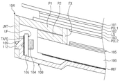
도 2는 도 1b에 도시된 도면을 설명하기 위한 확대도이다.Fig. 2 is an enlarged view for explaining the drawing shown in Fig. 1B.
도 2를 참조하면, 제1 편광판(POL1)은 상기 표시 패널(DPA)과 상기 윈도우(101) 사이에 제공될 수 있다. 상기 제1 편광판(POL1)은 제1 편광축(미도시)을 포함한다. 상기 제1 편광판(POL1)은 상기 표시 패널(DPA)로부터 수신 받은 광을 상기 제1 편광축과 평행한 방향으로 편광시킨다.Referring to FIG. 2, a first polarizer POL1 may be provided between the display panel DPA and the
제2 편광판(POL2)은 상기 표시 패널(DPA) 하측에 제공될 수 있다. 예를 들어 상기 제2 편광판(POL2)은 상기 하부 기판(103) 하면에 부착될 수 있다. 상기 제2 편광판(POL2)은 예를 들어 상기 하부 기판(103) 및 상기 복수의 광학 시트(105) 사이에 개재 된다. 상기 제2 편광판(POL2)은 제2 편광축(미도시)을 포함한다. 상기 제2 편광판(POL2)은 상기 복수의 광학 시트(105)로부터 수신 받은 광을 상기 제2 편광축과 평행한 방향으로 편광시킨다. 상기 제1 편광축과 상기 제2 편광축은 서로 수직할 수 있다.And the second polarizing plate POL2 may be provided below the display panel DPA. For example, the second polarizer POL2 may be attached to the lower surface of the
상기 도광판(106)의 하측에는 반사 필름(REF)이 제공될 수 있다. 예를 들어 상기 상기 반사 필름(REF)는 상기 도광판(106) 및 상기 바텀 샤시(108) 사이에 개재되며, 상기 반사 필름(REF)은 상기 도광판(106)의 하면에 부착될 수 있다. 상기 반사 필름(REF)은 상기 도광판(106)이 수신한 광 중에서 상기 반사 필름(REF) 측으로 누설된 광을 상측으로 반사시켜 광효율을 향상 시킬 수 있다. A reflective film REF may be provided on the lower side of the
상기 미들 샤시(104)는 제1 부(P1), 상기 제1 부(P1)의 일단으로부터 연장되는 연결부(FX), 상기 연결부(FX)로부터 연장되고 상기 제1 부(P1)의 적어도 일부분과 수직 방향으로 중첩되는 제2 부(P2), 및 상기 제1 부(P1)의 타단으로부터 연장되고 상기 바텀 샤시(108)와 체결되는 체결부(JNT)를 포함할 수 있다. The
상기 제1 부(P1)는 상기 광원(111)과 상기 수직 방향으로 중첩될 수 있다. 즉 상기 광원(111)의 상측에 상기 제1 부(P1)의 일부분이 배치될 수 있다. The first portion P1 may overlap with the
본 발명의 일 예로, 상기 연결부(FX)의 일부는 휘어진 형상을 가질 수 있다. 보다 구체적으로, 상기 연결부(FX)는 상기 제1 부(P1)와 상기 제2 부(P2) 사이에 정의되고, 상기 일방향과 평행한 만곡 기준선(미도시)을 중심으로 휘어진 곡면을 가질 수 있다.In an example of the present invention, a part of the connection portion FX may have a curved shape. More specifically, the connection part FX may be defined between the first part P1 and the second part P2, and may have a curved surface curved around a curved reference line (not shown) parallel to the one direction .
상기 곡면은 상기 일방향과 평행할 수 있다. 상기 연결부(FX)의 형상은 도 2에 도시된 형상에 한정되지 않고, 상기 만곡 기준선을 중심으로 여러가지 형상으로 휘어질 수 있다.The curved surface may be parallel to the one direction. The shape of the connection portion FX is not limited to the shape shown in FIG. 2, but can be bent in various shapes around the curvature reference line.
도 2에 도시된 바와 같이 상기 제1 부(P1)의 적어도 일부분은 상기 제2 부(P2)의 상측에 배치될 수 있다. 또한 상기 제2 부(P2)는 상기 제1 부(P1)의 적어도 일부분과 상기 수직 방향으로 소정 간격 이격될 수 있다.As shown in FIG. 2, at least a part of the first part P1 may be disposed above the second part P2. The second portion P2 may be spaced apart from the first portion P1 by a predetermined distance in the vertical direction.
그리고 상기 제1 부(P1)의 일부분은 상기 도광판(106)과 상기 수직 방향으로 중첩됨과 동시에 상기 제2 부(P2)와 수직 방향으로 중첩될 수 있고, 상기 제2 부(P2)의 일부분은 역시 상기 도광판(106)과 중첩될 수 있다.A part of the first part P1 may be overlapped with the
예를 들어, 도 2에서 도시한 바와 같이, 상기 제1 부(P1)의 상면은 상기 하부 기판(103)의 하면의 일부와 접촉될 수 있다. 상기 제2 부(P2)의 하면은 상기 도광판(106)의 상면의 일부와 접촉될 수 있다. 그리고 상기 연결부(FX)는 상기 하부 기판(103)의 하면의 일부와 상기 도광판(106)의 상면의 일부와 동시에 접촉될 수 있다. 좀 더 상세하게 설명하면 상기 연결부(FX)의 상면은 상기 하부 기판(103)의 하면의 일부와 접촉될 수 있고, 상기 연결부(FX)의 하면은 상기 도광판(106)의 상면의 일부와 접촉될 수 있다. For example, as shown in FIG. 2, the upper surface of the first portion P1 may be in contact with a lower surface of the
도 2에서는 상기 제2 부(P2)의 전체가 상기 도광판(106)의 일부분과 상기 수직 방향으로 중첩되어 있는 표시 장치(100)에 대해서 도시하고 있지만 이에 한정하지 않는다.Although FIG. 2 shows the
예를 들어, 상기 제2 부(P2)의 타단은 상기 입광면으로부터 상기 수직 방향으로 연장되는 제1 가상면(미도시)과 상기 회로기판(107)의 실장면(LF)으로부터 상기 수직 방향으로 연장되는 제2 가상면(미도시) 사이에 배치될 수 있다. 또한 상기 제1 가상면For example, the other end of the second portion P2 may extend from a first imaginary plane (not shown) extending in the vertical direction from the light incidence surface and a second imaginary plane (not shown) extending from the mount plane LF of the
본 발명의 일 예로, 상기 제1 부(P1)은 상기 광원(111)과 상기 수직 방향으로 중첩될 수 있고, 상기 제2 부(P2)는 평면상으로 상기 광원(111)과 이격되고, 상기 광원(111)과 상기 수직 방향으로 중첩되지 않을 수 있다.The first part P1 may overlap with the
그리고 상기 제1 부(P1) 및 상기 제2 부(P2)와 상기 복수의 광학 시트(105)는 평면상으로 이격될 수 있다. The first part (P1) and the second part (P2) and the plurality of optical sheets (105) may be spaced apart in a plane.
상기 바텀 샤시(108)는 상기 회로기판(107)과 결합될 수 있다. 예를 들어 상기 바텀 샤시(108)는 상기 회로기판(107)과 접착 부재(TAPE)에 의해 결합될 수 있다. The
전술한 바대로, 상기 바텀 샤시(108)는 상기 복수의 체결 후크(112)를 포함할 수 있고, 도 2에 도시된 바와 같이 상기 복수의 체결 홈(109)이 상기 복수의 체결 후크(112)와 각각 체결됨으로써 상기 미들 샤시(104)와 상기 바텀 샤시(108)가 서로 체결될 수 있다.As described above, the
상기 미들 샤시(104)와 상기 바텀 샤시(108)를 상기 복수의 체결 후크(112)와 상기 복수의 체결 홈(109)을 이용하여 체결함으로써, 상기 미들 샤시(104)를 고정 시키고, 상기 미들 샤시(104)가 외부의 충격 등에 의해 이탈되는 것을 방지할 수 있다. 따라서 도 2에 도시된 바와 같이 상기 표시 장치(100)의 최외곽에 배치되는 상기 미들 샤시(104)를 통해 상기 표시 장치(100)의 아웃라인(Outline)을 형성할 수 있다.The
나아가 상기 미들 샤시(104)는 상기 제1 부(P1), 상기 제2 부(P2), 및 상기 연결부(FX)를 구비함으로써, 기존 표시 장치의 몰드 프레임의 기능을 수행할 수 있다. 그리고 상기 미들 샤시(104)는 기존 표시 장치의 몰드 프레임보다 향상된 기능을 가질 수 있다.Furthermore, the
좀 더 상세하게 설명하면, 상기 제1 부(P1) 및 상기 제2 부(P2)가 상기 수직 방향으로 중첩되는 2중 샤시 구조를 가지는 상기 미들 샤시(104)가 상기 표시 패널(DPA) 및 상기 도광판(106) 사이에 배치될 수 있다. 그에 따라 상기 미들 샤시(104)는 휘어진 표시 패널과 도광판이 원래의 플랫(flat)한 형상으로 되돌아가려는 복원력을 상쇄시키는 방향으로 인장력을 상기 표시 패널과 상기 도광판에 작용시킴으로써, 커브드 표시 장치, 특히 상대적으로 큰 복원력이 발생되는 대형 커브드 표시 장치를 용이하게 구현할 수 있다.More specifically, the
결론적으로 기존의 몰드 프레임은 샤시에 비해 상대적으로 낮은 강도로 가지므로 대형 커브드 표시 장치에서 곡면 구현이 어려웠지만, 몰드 프레임을 상기 미들 샤시(104)로 대체하여, 커브드 표시 장치에 있어서 몰드 프레임의 단점을 개선할 수 있다.As a result, since the conventional mold frame has relatively lower strength than the chassis, it is difficult to realize a curved surface in the large curved display device, but the mold frame is replaced with the
도 3은 본 발명의 다른 일 실시예의 표시 장치를 설명하기 위한 확대 단면도이다.3 is an enlarged cross-sectional view for explaining a display device according to another embodiment of the present invention.
도 3의 표시 장치(100)는 도 2의 표시 장치(100)와 비교 했을 때 제1 접착 테이프(POR1) 및 제2 접착 테이프(POR2)를 더 포함할 수 있다.The
도 3에 도시된 바와 같이 상기 제1 접착 테이프(POR1)의 일면은 상기 도광판(106)에 부착될 수 있고 상기 제1 접착 테이프(POR1)의 타면은 상기 제2 부(P2)에 부착될 수 있다. 예를 들어 상기 제1 접착 테이프(POR1)의 일면은 상기 도광판(106)의 상면에 부착될 수 있고, 상기 제2 부(P2)의 하면에 부착될 수 있다.3, one surface of the first adhesive tape POR1 may be attached to the
상기 제2 접착 테이프(POR2)의 일면은 상기 표시 패널(DPA)에 부착될 수 있고 상기 제2 접착 테이프(POR2)의 타면은 상기 제1 부(P1)에 부착될 수 있다. 예를 들어, 상기 제2 접착 테이프(POR2)의 일면은 상기 표시 패널(DPA)의 상기 하부 기판(103)의 배면에 부착될 수 있고, 상기 제2 접착 테이프(POR2)의 타면은 상기 제1 부(P1)의 상면에 부착될 수 있다.One surface of the second adhesive tape POR2 may be attached to the display panel DPA and the other surface of the second adhesive tape POR2 may be attached to the first portion P1. For example, one surface of the second adhesive tape POR2 may be attached to the back surface of the
본 발명의 일 예에서, 상기 제1 접착 테이프(POR1) 및 상기 제2 접착 테이프(POR2)는 예를 들어 포론 소재를 포함하는 테이프일 수 있다. In one example of the present invention, the first adhesive tape POR1 and the second adhesive tape POR2 may be tape including, for example, a poron material.
도 3의 미들 샤시(104)는 상기 제1 접착 테이프(POR1) 및 상기 제2 접착 테이프(POR2)를 이용함으로써, 도 2의 표시 장치(100)과 비교했을 때 상기 표시 패널(DPA)과 상기 도광판(106)은 더 견고하게 상기 미들 샤시(104)에 결합 및 고정될 수 있다. 따라서 전술한 복원력을 상쇄시키는 방향으로 더 큰 인장력이 상기 표시 패널(DPA)과 상기 도광판(106)에 작용될 수 있고, 상기 표시 패널 및 상기 도광판의 휘어진 형상이 안정적으로 유지 될 수 있다.The
도 4는 본 발명의 다른 일 실시예의 표시 장치를 설명하기 위한 확대 단면도이다.4 is an enlarged cross-sectional view for explaining a display device according to another embodiment of the present invention.
도 4의 경우에는 도 3의 경우와 달리 상기 제2 부(P2)가 상기 제1 부(P1)의 상측에 배치될 수 있다. 도 4의 미들 샤시(104)도 상기 제1 부(P1)와 상기 제2 부(P2)가 상기 수직 방향으로 중첩되는 2중 샤시 구조를 구비할 수 있다. 나머지 구성은 도 3에 도시된 표시 장치(100)의 구성과 동일하다. 따라서 상기 2중 샤시 구조에 의한 효과도 전술한 바대로 동일하다.In the case of FIG. 4, the second part P2 may be disposed above the first part P1, unlike the case of FIG. The
도 5는 본 발명의 다른 일 실시예의 표시 장치(100)를 설명하기 위한 확대 단면도이다.5 is an enlarged cross-sectional view for explaining a
도 5를 참조하면, 상기 미들 샤시(104)는 상기 제1 부(P1),상기 제2 부(P2), 상기 제2 부(P2)로부터 연장되고, 상기 제1 부(P1) 및 상기 제2 부(P2)와 상기 수직 방향으로 중첩되는 제3 부(P3), 상기 제1 부(P1)와 상기 제2 부(P2)를 연결하는 제1 연결부(FX1), 상기 제2 부(P2)와 상기 제3 부(P3)를 연결하는 제2 연결부(FX2), 및 상기 체결부(JNT)를 포함할 수 있다. 5, the
도 5의 표시 장치(100)와 도 2의 표시 장치(100)는 미들 샤시(104)의 구조에서 차이가 있다. 상세하게 설명하면, 도 2의 연결부(FX)는 도 5의 제1 연결부(FX1)와 대응되는 바, 도 5의 미들 샤시(104)는 도 2의 미들 샤시(104)와 비교 했을때 상기 제3 부(P3) 및 상기 제2 연결부(FX2)를 더 포함한다. The
도 5에 도시된 바와 같이 상기 제2 부(P2)는 상기 제1 부(P1) 및 상기 제3 부(P3) 사이에 개재될 수 있다.As shown in FIG. 5, the second portion P2 may be interposed between the first portion P1 and the third portion P3.
본 발명의 일 예로, 상기 제1 연결부(FX1)의 일부는 휘어진 형상을 가질 수 있다.In an example of the present invention, a part of the first connection portion FX1 may have a curved shape.
보다 구체적으로 상기 제1 연결부(FX1)는 상기 제1 부(P1)와 상기 제2 부(P2) 사이에 정의되고, 상기 일방향과 평행한 제1 기준선(미도시)을 중심으로 휘어진 곡면을 가질 수 있다.More specifically, the first connection part FX1 is defined between the first part P1 and the second part P2 and has a curved surface curved around a first reference line (not shown) parallel to the one direction .
상기 제1 기준선을 중심으로 휘어진 곡면은 상기 일방향과 평행할 수 있다. 상기 제1 연결부(FX1)의 형상은 도 5에 도시된 형상에 한정되지 않고, 상기 제1 기준선을 중심으로 여러가지 형상으로 휘어질 수 있다.The curved surface curved around the first reference line may be parallel to the one direction. The shape of the first connection part FX1 is not limited to the shape shown in FIG. 5, but may be bent in various shapes around the first reference line.
마찬가지로 상기 제2 연결부(FX2)의 일부는 휘어진 형상을 가질 수 있다.Similarly, a part of the second connection portion FX2 may have a curved shape.
보다 구체적으로 상기 제2 연결부(FX2)는 상기 제2 부(P1)와 상기 제3 부(P2) 사이에 정의되고, 상기 일방향과 평행한 제2 기준선(미도시)을 중심으로 휘어진 곡면을 가질 수 있다.More specifically, the second connection part FX2 is defined between the second part P1 and the third part P2 and has a curved surface curved around a second reference line (not shown) parallel to the one direction .
상기 제2 기준선을 중심으로 휘어진 곡면은 상기 일방향과 평행할 수 있다. 상기 제2 연결부(FX2)의 형상은 도 5에 도시된 형상에 한정되지 않고, 상기 제2 기준선을 중심으로 여러가지 형상으로 휘어질 수 있다.The curved surface curved around the second reference line may be parallel to the one direction. The shape of the second connection portion FX2 is not limited to the shape shown in FIG. 5, but may be bent in various shapes around the second reference line.
나머지 구성에 대해서는 도 2에 도시된 표시 장치(100)의 구성과 동일한 바 생략하도록 한다.The rest of the configuration is the same as that of the
도 5에 도시된 상기 제1 부(P1), 상기 제2 부(P2), 상기 및 제3 부(P3)가 동시에 상기 수직 방향으로 중첩되는 3중 샤시 구조는 도 2의 2중 샤시 구조와 비교하여 보다 더 큰 강성을 가지고, 더 강한 인장력을 상기 도광판 및 상기 표시 패널에 작용시킬 수 있다. 따라서 상기 3중 샤시 구조가 상기 도광판(106)과 상기 하부 기판(103) 사이에 배치됨으로써, 커브드 표시 장치를 더욱 더 용이하게 구현할 수 있다. 도 5에서는 3중 샤시 구조만을 도시하였지만, 이에 한정되는 것은 아니고, 필요에 따라 3중 이상의 샤시 구조도 구현될 수 있을 것이다.The triple chassis structure in which the first portion P1, the second portion P2, the third portion P3, and the third portion P3 shown in FIG. 5 are simultaneously superimposed in the vertical direction, And a stronger tensile force can be applied to the light guide plate and the display panel. Accordingly, the triple chassis structure is disposed between the
도 6는 본 발명의 다른 일 실시예의 표시 장치를 설명하기 위한 확대 단면도이다.6 is an enlarged cross-sectional view for explaining a display device according to another embodiment of the present invention.
도 6의 경우에는 도 3의 경우와 달리 상기 체결부(JNT)와 상기 바텀 샤시(108)에 차이점이 있다. 6, there is a difference between the coupling portion JNT and the
도 6에 도시된 표시 장치는 상기 체결부(JNT) 및 상기 바텀 샤시(108)를 제외하고는 도 3의 표시 장치와 동일한 바, 중복되는 설명은 생략한다. 이하 도 6의 체결부(JNT)와 바텀 샤시(108)에 대해서 설명한다.The display device shown in FIG. 6 is the same as the display device of FIG. 3 except for the fastening portion JNT and the
본 발명의 일 예에서, 도 6의 체결부(JNT')는 도 3의 체결부(JNT)와 달리 상기 복수의 체결 홈(109)을 포함하지 않을 수 있으며 도 6의 바텀 샤시(108')는 도 3의 바텀 샤시(108)와 달리 상기 복수의 체결 후크(112)를 포함하지 않을 수 있다.6 may not include the plurality of
상기 체결부(JNT')는 제1 체결부(JNT1) 및 상기 제1 체결부(JNT1)로부터 연장되며 상기 제1 체결부(JNT1)의 적어도 일부분과 수평 방향으로 중첩되는 제2 체결부(JNT2)를 포함할 수 있다.The fastening part JNT 'includes a first fastening part JNT1 and a second fastening part JNT2 extending from the first fastening part JNT1 and overlapping at least a part of the first fastening part JNT1 in a horizontal direction. ).
상기 바텀 샤시(108')는 제3 체결부(JNT3) 및 상기 제3 체결부(JNT3)로부터 연장되며, 상기 제3 체결부(JNT3)의 적어도 일부분과 상기 수평 방향으로 중첩되는 제4 체결부(JNT4)를 포함할 수 있다.The bottom chassis 108 'extends from the third fastening portion JNT3 and the third fastening portion JNT3 and is connected to at least a portion of the third fastening portion JNT3, (JNT4).
본 발명의 일 예에서, 상기 제3 체결부(JNT3)와 상기 회로기판(107)은 상기 접착 부재(TAPE)에 의해 결합될 수 있다.In an embodiment of the present invention, the third fastening portion JNT3 and the
상기 제1 체결부(JNT1)과 상기 제2 체결부(JNT2)는 수평 방향으로 중첩되면서 서로 결합될 수 있다.The first fastening part JNT1 and the second fastening part JNT2 may be coupled to each other while being overlapped in the horizontal direction.
상기 제3 체결부(JNT3)과 상기 제4 체결부(JNT4)는 상기 수평 방향으로 중첩되면서 서로 결합될 수 있다.The third fastening part JNT3 and the fourth fastening part JNT4 may be coupled to each other while being overlapped in the horizontal direction.
상기 제1 체결부(JNT1), 상기 제3 체결부(JNT3)는 상기 제2 체결부(JNT2)와 상기 제4 체결부(JNT4)와 상기 수평 방향으로 중첩될 수 있다.The first fastening part JNT1 and the third fastening part JNT3 may be overlapped with the second fastening part JNT2 and the fourth fastening part JNT4 in the horizontal direction.
상기 제2 체결부(JNT2)와 상기 제4 체결부(JNT4)는 상기 수직 방향으로 중첩될 수 있다.The second fastening part JNT2 and the fourth fastening part JNT4 may be overlapped in the vertical direction.
상기 제2 체결부(JNT2)의 일단은 상기 제4 체결부(JNT4)의 일단과 체결될 수 있다.One end of the second fastening part JNT2 may be fastened to one end of the fourth fastening part JNT4.
예를 들어 도 6에 도시된 바와 같이 상기 제2 체결부(JNT2)의 일단과 상기 제4 체결부(JNT4)의 일단은 서로 접촉할 수 있다. 좀 더 상세하게 설명하면 상기 제2 체결부(JNT2)의 일단과 상기 제4 체결부(JNT4)의 일단은 접착성 부재에 의해서 서로 부착됨으로써, 체결될 수 있다. For example, as shown in FIG. 6, one end of the second fastening portion JNT2 and one end of the fourth fastening portion JNT4 may contact each other. In more detail, one end of the second fastening portion JNT2 and one end of the fourth fastening portion JNT4 are attached to each other by an adhesive member, so that they can be fastened.
결론적으로, 상기 제2 체결부(JNT2)의 일단과 상기 제4 체결부(JNT4)의 일단이 체결되어 형성되는 구조를 상기 복수의 체결 홈(109) 및 체결 후크(112) 구조를 대신하여 적용함으로써, 높은 강성을 가지는 커브드 표시 장치의 샤시 구조를 구현할 수 있다.As a result, a structure in which one end of the second fastening portion JNT2 and one end of the fourth fastening portion JNT4 are coupled to each other may be applied instead of the plurality of fastening recesses 109 and the fastening hooks 112 The chassis structure of the curved display device having high rigidity can be realized.
따라서 미들 샤시(104)와 바텀 샤시(108)의 체결이 해제되어 샤시가 이탈되는 위험성을 도 3의 표시 장치(100)에 비해서 감소시킬 수 있다. Therefore, the risk that the engagement between the
도 7는 본 발명의 다른 일 실시예의 표시 장치(100)를 설명하기 위한 확대 단면도이다.7 is an enlarged cross-sectional view for explaining a
도 7을 참조하면, 본 발명의 일 실시예에서, 상기 체결부(JNT)의 두께는 제1 부(P1)의 두께와 상이할 수 있다. 나아가 상기 체결부(JNT)의 두께와 제2 부(P2)의 두께는 상이할 수 있다.Referring to FIG. 7, in an embodiment of the present invention, the thickness of the fastening portion JNT may be different from the thickness of the first portion P1. Further, the thickness of the coupling portion JNT may be different from the thickness of the second portion P2.
예를 들어 상기 제1 부(P1)와 상기 제2 부(P2)의 두께는 상기 체결부(JNT)의 두께보다 클 수 있다.For example, the thickness of the first portion P1 and the second portion P2 may be greater than the thickness of the fastening portion JNT.
도 7과 같이 상대적으로 높은 인장력이 필요한 상기 제1 부(P1)와 상기 제2 부(P2) 만을 상기 체결부(JNT)보다 두껍게 제작하여, 재료 비용을 절감하면서, 전술한 효과를 달성할 수 있다.Only the first portion P1 and the second portion P2 that require a relatively high tensile force as shown in FIG. 7 are made thicker than the fastening portion JNT, thereby achieving the above-mentioned effect while reducing the material cost have.
도 8은 본 발명의 일 실시예에 따른 표시 장치의 제조 방법의 순서도이다.8 is a flowchart of a method of manufacturing a display device according to an embodiment of the present invention.
도 8을 참조하면, 본 발명의 표시 장치(100)를 제조하는데 있어서, 우선적으로 샤시 부재(미도시)를 제공한다.(S1) 상기 샤시 부재는 사출 성형 방법을 통해 성형될 수 있다. 상기 샤시 부재는 장변과 단변을 가지는 얇은 판상 형상일 수 있다.8, in manufacturing the
상기 샤시 부재는 금속 재질로 이루어질 수 있다. 예를 들어, 상기 샤시 부재는 알루미늄(Al), 철(Fe), 구리(Cu), 이들을 포함한 화합물 및 혼합물을 포함할 수 있다.The chassis member may be made of a metal material. For example, the chassis member may comprise aluminum (Al), iron (Fe), copper (Cu), compounds and mixtures thereof.
상기 샤시 부재는 제1 부(P1) 및 제2 부(P2) 및 상기 제1 부(P1)와 상기 제2 부(P2)를 연결하는 연결부(FX)를 포함할 수 있다.The chassis member may include a first portion P1 and a second portion P2 and a connection portion FX connecting the first portion P1 and the second portion P2.
도 2의 미들 샤시(104)를 제작하기 위해서 상기 제1 연결부(FX1)를 구부린다.(S2) 좀 더 상세하게 설명하면, 상기 제1 부(P1) 및 상기 제2 부(P2)가 수직 방향으로 중첩되도록 상기 제1 연결부(FX1)를 구부린다.The first connecting portion FX1 is bent in order to manufacture the
다음으로 상기 S2 과정을 통해 제작된 상기 미들 샤시(104)의 일부분이 도광판(106)과 표시 패널(DPA)의 사이에 개재되도록 상기 도광판(106)과 상기 표시 패널(DPA)을 배치한다.(S3) Next, the
좀 더 상세하게 설명하면, 상기 제1 부(P1) 및 상기 제2 부(P2)를 상기 도광판(106)의 일단 및 상기 표시 패널(DPA)의 일단 사이에 개재되도록 상기 도광판(106) 및 상기 표시 패널(DPA)을 배치한다.More specifically, the first portion P1 and the second portion P2 may be disposed between the
상기 S1 내지 S3 과정을 통해서 도 2에 도시된 표시 장치(100)가 제조될 수 있다.The
상기 S3 단계 이후에 제1 접착 테이프(POR1)의 일면은 상기 도광판(106)에 부착시키고, 상기 제1 접착 테이프(POR1)의 타면은 상기 제2 부(P2)에 부착시키고(S4), 상기 제2 접착 테이프(POR2)의 일면은 표시 패널(DPA)에 부착시키고, 상기 제2 접착 테이프(POR2)의 타면은 상기 제1 부(P1)에 부착시킬 수 있다.(S5) 상기 S4 내지 S5 과정을 통해 도 3에 도시된 표시 장치(100)를 제조할 수 있다.After step S3, one side of the first adhesive tape POR1 is attached to the
나아가 도 5에 도시된 3중 샤시 구조의 미들 샤시(104)를 포함하는 표시 장치(100)를 제조하기 위하여, 상기 샤시 부재의 제3 부(P3)가 상기 제1 부(P1) 및 상기 제2 부(P2)와 상기 수직방향으로 중첩되도록 상기 제2 부(P2)와 상기 제3 부(P3)를 연결하는 제2 연결부(FX2)를 구부리는 단계를 더 포함할 수 있다.In order to manufacture the
이상 실시예를 참조하여 설명하였지만, 해당 기술 분야의 숙련된 당업자는 하기의 특허 청구 범위에 기재된 본 발명의 사상 및 영역으로부터 벗어나지 않는 범위 내에서 본 발명을 다양하게 수정 및 변경시킬 수 있음을 이해할 수 있을 것이다.It will be apparent to those skilled in the art that various modifications and variations can be made in the present invention without departing from the spirit or scope of the invention as defined in the following claims. There will be.
P1: 제1 부
P2: 제2 부
FX: 연결부
106: 도광판
104: 미들 샤시
108: 바텀 샤시P1:
FX: connection part 106: light guide plate
104: Middle Chassis 108: Bottom Chassis
Claims (20)
상기 광원과 대향하는 입광면을 구비하는 도광판;
상기 도광판 상에 배치되는 미들 샤시; 및
상기 미들 샤시 상에 배치되는 표시 패널을 포함하고,
상기 미들 샤시는 제1 부, 상기 제1 부의 일단으로부터 연장되는 연결부, 및 상기 연결부로부터 연장되고 상기 제1 부의 적어도 일부분과 수직 방향으로 소정 간격 이격되고, 상기 수직 방향으로 중첩되는 제2 부를 포함하는 것을 특징으로 하는 표시 장치.
Light source;
A light guide plate having a light incidence surface facing the light source;
A middle chassis disposed on the light guide plate; And
And a display panel disposed on the middle chassis,
The middle chassis includes a first portion, a connection portion extending from one end of the first portion, and a second portion extending from the connection portion and spaced apart from the first portion by a predetermined distance in the vertical direction and overlapping in the vertical direction And the display device.
상기 연결부는 상기 제1 부와 상기 제2 부 사이에 정의되는 만곡 기준선을 중심으로 휘어지는 것을 특징으로 하는 표시 장치.
The method according to claim 1,
Wherein the connection portion is bent about a curvature reference line defined between the first portion and the second portion.
상기 광원은 상기 도광판의 일측에 배치되고,
상기 제1 부는 상기 광원과 상기 수직 방향으로 중첩되고, 상기 제2 부는 평면상으로 상기 광원과 이격된 것을 특징으로 하는 표시 장치.
3. The method of claim 2,
Wherein the light source is disposed on one side of the light guide plate,
Wherein the first portion overlaps with the light source in the vertical direction, and the second portion is spaced apart from the light source in a plane.
상기 광원이 실장되는 실장면을 포함하는 회로기판을 더 포함하고,
상기 제2 부는 일단은 상기 연결부에 연결되고, 평면상으로 보았을 때, 상기 제2 부의 타단은 상기 입광면으로부터 상기 수직 방향으로 연장되는 제1 가상면과 상기 실장면으로부터 상기 수직 방향으로 연장되는 제2 가상면 사이에 배치되는 것을 특징으로 하는 표시 장치.
The method of claim 3,
And a circuit board including a mounting surface on which the light source is mounted,
Wherein the second portion is connected to the connection portion at one end and the other end of the second portion is connected to the first imaginary plane extending in the vertical direction from the light incidence surface and the second imaginary plane extending in the vertical direction from the mount portion, 2 virtual planes.
제1 접착 테이프 및 제2 접착 테이프를 더 포함하고,
상기 제1 부는 상기 제2 부의 상측에 배치되며,
상기 제1 접착 테이프의 일면은 상기 도광판에 부착되고, 상기 제1 접착 테이프의 타면은 상기 제2 부에 부착되고,
상기 제2 접착 테이프의 일면은 상기 표시 패널에 부착되고, 상기 제2 접착 테이프의 타면은 상기 제1 부에 부착되는 것을 특징으로 하는 표시 장치.
The method according to claim 1,
Further comprising a first adhesive tape and a second adhesive tape,
Wherein the first portion is disposed on the upper side of the second portion,
One surface of the first adhesive tape is attached to the light guide plate, the other surface of the first adhesive tape is attached to the second portion,
Wherein one surface of the second adhesive tape is attached to the display panel and the other surface of the second adhesive tape is attached to the first portion.
상기 미들 샤시는 상기 제2 부로부터 연장되고 상기 제1 및 제2 부와 상기 수직 방향으로 중첩되는 제3 부를 더 포함하는 것을 특징으로 하는 표시 장치.
The method according to claim 1,
Wherein the middle chassis further comprises a third portion extending from the second portion and overlapping the first and second portions in the vertical direction.
상기 제2 부는 상기 제1 및 제3 부 사이에 개재되는 것을 특징으로 하는 표시 장치.
The method according to claim 6,
And the second portion is interposed between the first and third portions.
상기 제1 부와 상기 제2 부를 연결하는 제1 연결부, 및 상기 제2 부와 상기 제3 부를 연결하는 제2 연결부를 더 포함하며,
상기 제1 연결부는 상기 제1 부와 상기 제2 부 사이에 정의되는 제1 기준선을 중심으로 휘어지고,
상기 제2 연결부는 상기 제2 부와 상기 제3 부 사이에 정의되는 제2 기준선을 중심으로 휘어지는 것을 특징으로 하는 표시 장치.
8. The method of claim 7,
A first connecting portion connecting the first portion and the second portion, and a second connecting portion connecting the second portion and the third portion,
Wherein the first connection portion is bent around a first reference line defined between the first portion and the second portion,
And the second connection portion is bent about a second reference line defined between the second portion and the third portion.
상기 도광판 및 상기 광원을 수납하는 수납공간이 정의된 바텀 샤시를 더 포함하고,
상기 미들 샤시는 상기 제1 부의 타단으로부터 연장되고, 상기 바텀 샤시와 체결되는 체결부를 더 포함하는 것을 특징으로 하는 표시 장치.
The method according to claim 1,
Further comprising a bottom chassis in which a storage space for storing the light guide plate and the light source is defined,
Wherein the middle chassis further comprises a fastening part extending from the other end of the first part and fastened to the bottom chassis.
상기 체결부는 제1 체결부 및 상기 제1 체결부로부터 연장되며, 상기 제1 체결부의 적어도 일부분과 수평방향으로 중첩되는 제2 체결부를 포함하며,
상기 바텀 샤시는 제3 체결부 및 상기 제3 체결부로부터 연장되며, 상기 제3 체결부의 적어도 일부분과 상기 수평 방향으로 중첩되는 제4 체결부를 포함하며,
상기 제2 체결부는 상기 제4 체결부와 체결되는 것을 특징으로 하는 표시 장치.
10. The method of claim 9,
Wherein the fastening portion includes a first fastening portion and a second fastening portion extending from the first fastening portion and horizontally overlapping at least a portion of the first fastening portion,
Wherein the bottom chassis includes a third fastening portion and a fourth fastening portion extending from the third fastening portion and overlapping at least a part of the third fastening portion in the horizontal direction,
And the second fastening portion is fastened to the fourth fastening portion.
상기 광원이 실장되는 회로기판을 더 포함하며,
상기 회로기판은 상기 제3 체결부에 결합되는 것을 특징으로 하는 표시 장치.
11. The method of claim 10,
And a circuit board on which the light source is mounted,
And the circuit board is coupled to the third fastening portion.
상기 제1 부의 두께와 상기 체결부의 두께는 서로 상이한 것을 특징으로 하는 표시 장치.
10. The method of claim 9,
Wherein the thickness of the first portion and the thickness of the fastening portion are different from each other.
상기 광원과 대향하는 입광면을 구비하는 도광판;
상기 도광판 및 상기 광원을 수납하는 수납공간이 정의된 바텀 샤시; 및
상기 도광판 상에 배치되는 미들 샤시를 포함하고,
상기 미들 샤시는 제1 부, 상기 제1 부의 일단으로부터 연장되는 연결부, 상기 연결부로부터 연장되고 상기 제1 부의 적어도 일부분과 수직 방향으로 소정 간격 이격되고, 상기 수직 방향으로 중첩되는 제2 부, 및 상기 제1 부의 타측으로부터 연장되고, 상기 바텀 샤시와 체결되는 체결부를 포함하는 것을 특징으로 하는 백라이트 유닛.
Light source;
A light guide plate having a light incidence surface facing the light source;
A bottom chassis defining a storage space for storing the light guide plate and the light source; And
And a middle chassis disposed on the light guide plate,
The middle chassis includes a first portion, a connecting portion extending from one end of the first portion, a second portion extending from the connecting portion, spaced apart from the first portion by a predetermined distance in the vertical direction, And a fastening portion extending from the other side of the first portion and fastened to the bottom chassis.
접착 테이프를 더 포함하며,
상기 제1 부는 상기 제2 부의 상측에 배치되며,
상기 접착 테이프의 일면은 상기 도광판에 부착되고, 상기 접착 테이프의 타면은 상기 제2 부에 부착되는 것을 특징으로 하는 백라이트 유닛.
14. The method of claim 13,
Further comprising an adhesive tape,
Wherein the first portion is disposed on the upper side of the second portion,
Wherein one surface of the adhesive tape is attached to the light guide plate, and the other surface of the adhesive tape is attached to the second portion.
접착 테이프를 더 포함하며,
상기 제1 부는 상기 제2 부의 하측에 배치되며,
상기 접착 테이프의 일면은 상기 도광판에 부착되고, 상기 접착 테이프의 타면은 상기 제1 부에 부착되는 것을 특징으로 하는 백라이트 유닛.
14. The method of claim 13,
Further comprising an adhesive tape,
Wherein the first portion is disposed below the second portion,
Wherein one surface of the adhesive tape is attached to the light guide plate, and the other surface of the adhesive tape is attached to the first portion.
복수의 광학 시트를 더 포함하며,
상기 복수의 광학 시트는 상기 도광판 상측에 배치되고, 상기 제1 부 및 상기 제2 부와 평면상으로 보았을 때 이격되는 것을 특징으로 하는 백라이트 유닛.
14. The method of claim 13,
Further comprising a plurality of optical sheets,
Wherein the plurality of optical sheets are disposed on the upper side of the light guide plate and spaced apart from each other when viewed in a plan view from the first portion and the second portion.
상기 미들 샤시는 상기 제2 부로부터 연장되고 상기 제1 및 제2 부와 상기 수직 방향으로 중첩되는 제3 부를 더 포함하는 것을 특징으로 하는 백라이트 유닛.
14. The method of claim 13,
Wherein the middle chassis further comprises a third portion extending from the second portion and overlapping the first and second portions in the vertical direction.
상기 샤시 부재로부터 미들 샤시를 제작하는 단계; 및
상기 미들 샤시가 도광판의 일단 및 표시 패널의 일단과 수직 방향으로 중첩하도록 상기 도광판 및 상기 표시 패널을 상기 미들 샤시와 결합 시키는 단계를 포함하고,
상기 미들 샤시를 제작하는 단계는 상기 샤시 부재의 제1 및 제2 부가 상기 수직 방향으로 중첩되도록, 상기 제1 부 및 상기 제2 부를 연결하는 제1 연결부를 구부리는 단계를 포함하는 표시 장치 제조 방법.
Providing a chassis member;
Fabricating a middle chassis from the chassis member; And
And coupling the light guide plate and the display panel to the middle chassis so that the middle chassis overlaps one end of the light guide plate and one end of the display panel in a vertical direction,
Wherein the step of fabricating the middle chassis includes bending a first connection portion connecting the first portion and the second portion so that the first and second portions of the chassis member overlap in the vertical direction, .
상기 제1 부가 상기 제2 부의 상측에 배치되고,
상기 미들 샤시와 결합 시키는 단계는
제1 접착 테이프의 일면은 도광판에 부착시키고, 상기 제1 접착 테이프의 타면은 상기 제2 부에 부착시키는 단계; 및
상기 제2 접착 테이프의 일면은 표시 패널에 부착시키고, 상기 제2 접착 테이프의 타면은 상기 제1 부에 부착시키는 단계를 포함하는 것을 특징으로 하는 표시 장치 제조 방법.
19. The method of claim 18,
The first portion is disposed on the upper side of the second portion,
The step of combining with the middle chassis
Attaching one surface of the first adhesive tape to the light guide plate and attaching the other surface of the first adhesive tape to the second portion; And
And attaching one surface of the second adhesive tape to the display panel and attaching the other surface of the second adhesive tape to the first portion.
상기 미들 샤시를 제작하는 단계는 제3 부가 상기 제1 부 및 상기 제2 부와 상기 수직방향으로 중첩되도록 상기 제2 부와 상기 제3 부를 연결하는 제2 연결부를 구부리는 단계를 더 포함하는 표시 장치 제조 방법.
19. The method of claim 18,
Wherein the step of fabricating the middle chassis further comprises bending a second connection portion connecting the second portion and the third portion so that the third portion overlaps the first portion and the second portion in the vertical direction, Device manufacturing method.
Priority Applications (4)
| Application Number | Priority Date | Filing Date | Title |
|---|---|---|---|
| KR1020150154074A KR102451998B1 (en) | 2015-11-03 | 2015-11-03 | Display device and fabricating mehtod of the same |
| US15/196,204 US10254470B2 (en) | 2015-11-03 | 2016-06-29 | Display device and method of manufacturing the same |
| CN201610957929.2A CN106842693B (en) | 2015-11-03 | 2016-10-27 | Backlight unit, display device and method of manufacturing the same |
| US15/977,524 US20180259704A1 (en) | 2015-11-03 | 2018-05-11 | Display device |
Applications Claiming Priority (1)
| Application Number | Priority Date | Filing Date | Title |
|---|---|---|---|
| KR1020150154074A KR102451998B1 (en) | 2015-11-03 | 2015-11-03 | Display device and fabricating mehtod of the same |
Publications (2)
| Publication Number | Publication Date |
|---|---|
| KR20170052760A true KR20170052760A (en) | 2017-05-15 |
| KR102451998B1 KR102451998B1 (en) | 2022-10-11 |
Family
ID=58634509
Family Applications (1)
| Application Number | Title | Priority Date | Filing Date |
|---|---|---|---|
| KR1020150154074A KR102451998B1 (en) | 2015-11-03 | 2015-11-03 | Display device and fabricating mehtod of the same |
Country Status (3)
| Country | Link |
|---|---|
| US (1) | US10254470B2 (en) |
| KR (1) | KR102451998B1 (en) |
| CN (1) | CN106842693B (en) |
Cited By (1)
| Publication number | Priority date | Publication date | Assignee | Title |
|---|---|---|---|---|
| KR20190108665A (en) * | 2018-03-14 | 2019-09-25 | 삼성디스플레이 주식회사 | Display module and display device including the same |
Families Citing this family (9)
| Publication number | Priority date | Publication date | Assignee | Title |
|---|---|---|---|---|
| JP6517724B2 (en) * | 2016-04-08 | 2019-05-22 | ミネベアミツミ株式会社 | Planar lighting device |
| KR101866314B1 (en) * | 2016-07-12 | 2018-06-12 | (주)코텍 | Curved type display device |
| CN107390416A (en) * | 2017-09-19 | 2017-11-24 | 合肥惠科金扬科技有限公司 | Display module, display screen and electronic product |
| KR20190034368A (en) * | 2017-09-22 | 2019-04-02 | 삼성디스플레이 주식회사 | Backlight unit and display device including the same |
| TWM557369U (en) * | 2017-11-09 | 2018-03-21 | 揚昇照明股份有限公司 | Reflective display apparatus |
| KR20190079727A (en) * | 2017-12-27 | 2019-07-08 | 삼성디스플레이 주식회사 | Display device |
| CN110646963A (en) * | 2018-06-26 | 2020-01-03 | 鸿富锦精密工业(深圳)有限公司 | Liquid crystal display module and display device |
| CN110646964A (en) * | 2018-06-27 | 2020-01-03 | 夏普株式会社 | Liquid crystal display device having a plurality of pixel electrodes |
| CN110673252B (en) * | 2019-09-12 | 2021-09-03 | 惠州市华星光电技术有限公司 | Light guide plate and display device thereof |
Citations (3)
| Publication number | Priority date | Publication date | Assignee | Title |
|---|---|---|---|---|
| JP2012118498A (en) * | 2010-12-03 | 2012-06-21 | Wistron Corp | Flat panel display |
| JP2012198434A (en) * | 2011-03-22 | 2012-10-18 | Japan Display East Co Ltd | Liquid crystal display device |
| KR20150092408A (en) * | 2014-02-04 | 2015-08-13 | 삼성디스플레이 주식회사 | Curved backlight assembly and curved display device having the same |
Family Cites Families (16)
| Publication number | Priority date | Publication date | Assignee | Title |
|---|---|---|---|---|
| JP3511591B2 (en) * | 1999-07-05 | 2004-03-29 | 株式会社アドバンスト・ディスプレイ | Liquid crystal display |
| JP2003346535A (en) * | 2002-03-20 | 2003-12-05 | Advanced Display Inc | Planar light device and display device |
| US7153018B2 (en) * | 2002-09-19 | 2006-12-26 | Matsushita Electric Industrial Co., Ltd. | Illumination unit and liquid crystal display comprising it |
| TWI348055B (en) * | 2005-10-18 | 2011-09-01 | Coretronic Corp | Plane light source apparatus |
| BRPI0721020A2 (en) * | 2007-01-22 | 2014-07-29 | Sharp Kk | REAR LIGHT DEVICE AND FLAT DISPLAY Using the same |
| KR101014464B1 (en) * | 2009-01-13 | 2011-02-14 | 엘지디스플레이 주식회사 | Liquid crystal display device |
| JP5394492B2 (en) * | 2009-07-29 | 2014-01-22 | アルプス電気株式会社 | Operating device |
| EP2641179B1 (en) * | 2010-11-21 | 2019-01-02 | Verifyter AB | Method and apparatus for automatic diagnosis of software failures |
| KR101926430B1 (en) * | 2011-04-18 | 2018-12-10 | 엘지디스플레이 주식회사 | Display apparatus |
| JP2013003487A (en) | 2011-06-21 | 2013-01-07 | Panasonic Liquid Crystal Display Co Ltd | Display device |
| KR101909436B1 (en) | 2012-08-10 | 2018-10-18 | 엘지디스플레이 주식회사 | Display apparatus and method for manufacturing the same |
| TWI464501B (en) * | 2012-08-28 | 2014-12-11 | Au Optronics Corp | Structural support and panel display module therewith |
| KR101966739B1 (en) | 2012-11-09 | 2019-04-09 | 삼성전자주식회사 | Curved display apparatus |
| KR101472752B1 (en) * | 2012-12-24 | 2014-12-15 | 엘지디스플레이 주식회사 | Liquid crystal display device |
| KR102232166B1 (en) * | 2014-03-06 | 2021-03-29 | 삼성디스플레이 주식회사 | Display apparatus |
| WO2016046973A1 (en) * | 2014-09-26 | 2016-03-31 | 堺ディスプレイプロダクト株式会社 | Display device |
-
2015
- 2015-11-03 KR KR1020150154074A patent/KR102451998B1/en active IP Right Grant
-
2016
- 2016-06-29 US US15/196,204 patent/US10254470B2/en active Active
- 2016-10-27 CN CN201610957929.2A patent/CN106842693B/en active Active
Patent Citations (3)
| Publication number | Priority date | Publication date | Assignee | Title |
|---|---|---|---|---|
| JP2012118498A (en) * | 2010-12-03 | 2012-06-21 | Wistron Corp | Flat panel display |
| JP2012198434A (en) * | 2011-03-22 | 2012-10-18 | Japan Display East Co Ltd | Liquid crystal display device |
| KR20150092408A (en) * | 2014-02-04 | 2015-08-13 | 삼성디스플레이 주식회사 | Curved backlight assembly and curved display device having the same |
Cited By (1)
| Publication number | Priority date | Publication date | Assignee | Title |
|---|---|---|---|---|
| KR20190108665A (en) * | 2018-03-14 | 2019-09-25 | 삼성디스플레이 주식회사 | Display module and display device including the same |
Also Published As
| Publication number | Publication date |
|---|---|
| US20170123144A1 (en) | 2017-05-04 |
| US10254470B2 (en) | 2019-04-09 |
| KR102451998B1 (en) | 2022-10-11 |
| CN106842693A (en) | 2017-06-13 |
| CN106842693B (en) | 2021-08-27 |
Similar Documents
| Publication | Publication Date | Title |
|---|---|---|
| KR102451998B1 (en) | Display device and fabricating mehtod of the same | |
| US8531624B2 (en) | LCD device | |
| KR100759736B1 (en) | Liquid-crystal display device | |
| US8134658B2 (en) | Liquid crystal display module | |
| US9291853B2 (en) | Display device | |
| US9467641B2 (en) | Television and electronic apparatus | |
| US20070132909A1 (en) | Liquid crystal display device | |
| US20070252922A1 (en) | Liquid crystal display device | |
| EP2153273B1 (en) | Display device | |
| US8780293B2 (en) | Liquid crystal display device, backlight module and frame unit thereof | |
| TWI459091B (en) | Backlight module and display device using the same | |
| US20130077343A1 (en) | Backlight unit and display apparatus having the same | |
| EP3089140B1 (en) | Display apparatus | |
| US10345510B2 (en) | Liquid crystal display | |
| KR20180067797A (en) | Electronic device | |
| JP7064264B2 (en) | Display device | |
| US10139544B2 (en) | Light guide plate, back plate, edge-lit type backlight module and display device | |
| KR102227016B1 (en) | Display Device | |
| US9341876B2 (en) | Liquid crystal display device | |
| EP2755079A2 (en) | Display apparatus | |
| KR101693045B1 (en) | Liquid Cyrstal Display device | |
| US20140085576A1 (en) | Light Guide Plates and Optical Films with Mating Alignment Features | |
| US9164304B2 (en) | Liquid crystal display assembly and electronic device | |
| KR101269292B1 (en) | Liquid Crystal Display Device | |
| US9395567B2 (en) | Display device and liquid crystal display device that prevent cracking of a display panel without increasing in size |
Legal Events
| Date | Code | Title | Description |
|---|---|---|---|
| A201 | Request for examination | ||
| E902 | Notification of reason for refusal | ||
| E701 | Decision to grant or registration of patent right | ||
| GRNT | Written decision to grant |