KR20170013802A - Plsmonic device - Google Patents
Plsmonic device Download PDFInfo
- Publication number
- KR20170013802A KR20170013802A KR1020160036323A KR20160036323A KR20170013802A KR 20170013802 A KR20170013802 A KR 20170013802A KR 1020160036323 A KR1020160036323 A KR 1020160036323A KR 20160036323 A KR20160036323 A KR 20160036323A KR 20170013802 A KR20170013802 A KR 20170013802A
- Authority
- KR
- South Korea
- Prior art keywords
- filter
- spp mode
- spp
- converter
- mode
- Prior art date
Links
Images


Classifications
-
- G—PHYSICS
- G02—OPTICS
- G02B—OPTICAL ELEMENTS, SYSTEMS OR APPARATUS
- G02B6/00—Light guides; Structural details of arrangements comprising light guides and other optical elements, e.g. couplings
- G02B6/10—Light guides; Structural details of arrangements comprising light guides and other optical elements, e.g. couplings of the optical waveguide type
- G02B6/12—Light guides; Structural details of arrangements comprising light guides and other optical elements, e.g. couplings of the optical waveguide type of the integrated circuit kind
- G02B6/122—Basic optical elements, e.g. light-guiding paths
- G02B6/1226—Basic optical elements, e.g. light-guiding paths involving surface plasmon interaction
-
- G—PHYSICS
- G02—OPTICS
- G02B—OPTICAL ELEMENTS, SYSTEMS OR APPARATUS
- G02B5/00—Optical elements other than lenses
- G02B5/008—Surface plasmon devices
-
- G—PHYSICS
- G02—OPTICS
- G02B—OPTICAL ELEMENTS, SYSTEMS OR APPARATUS
- G02B5/00—Optical elements other than lenses
- G02B5/20—Filters
- G02B5/28—Interference filters
- G02B5/285—Interference filters comprising deposited thin solid films
- G02B5/288—Interference filters comprising deposited thin solid films comprising at least one thin film resonant cavity, e.g. in bandpass filters
Landscapes
- Physics & Mathematics (AREA)
- General Physics & Mathematics (AREA)
- Optics & Photonics (AREA)
- Engineering & Computer Science (AREA)
- Microelectronics & Electronic Packaging (AREA)
- Optical Integrated Circuits (AREA)
Abstract
Description
본 발명은 플라즈모닉 소자에 관한 것으로, 보다 상세하게는, 도파로 내부에서 모드 변화를 일으키는 수동 소자를 개선시킨 플라즈모닉 소자에 관한 것이다.BACKGROUND OF THE
플라즈몬은 금속 내부 자유전자밀도의 진동에 해당되는 collective excitation이다. 전자밀도는 전자기장과 상호작용하므로 광자와 플라즈몬은 결합할 수 있으며 금속 표면의 플라즈몬과 광자가 결합된 표면 모드 (coupled surface mode)를 표면 플라즈몬 폴라리톤이라고 부른다. 이러한 표면 모드는 회절한계 이상으로 빛을 집속하는 것이 가능하도록 하므로 광학 저장매체나 광 집적회로, 비선형 광학 연구 등에서 그 응용 가능성이 높다고 평가된다. Plasmon is a collective excitation corresponding to the oscillation of free electron density in the metal. The electron density interacts with the electromagnetic field, so that the photon and plasmon can combine. The coupled surface mode in which the plasmon and photons on the metal surface are combined is called surface plasmon polariton. These surface modes allow the light to be focused above the diffraction limit, which is considered to be highly applicable in optical storage media, optical integrated circuits, and nonlinear optical research.
가장 간단한 플라즈모닉 소자 중 하나로 SPP가 전파되는 통로인 도파로를 들 수 있다. 도파로는 형태와 크기에 따라 분산관계 (dispersion relation)와 전파 거리 (propagation length) 등의 전파 특성이 달라지며, 도파로 설계를 통해 이러한 특성들을 조절하는 것도 가능하다. 도파로는 여러 개의 전파 모드를 가질 수 있는데 각각의 모드를 결합시키는 구조가 없는 한 각각의 모드들은 독립적인 전파 채널로 동작하며 이를 이용한 멀티플렉싱도 가능하다. One of the simplest plasmonic elements is a waveguide that is the path through which the SPP propagates. Propagation characteristics such as dispersion relation and propagation length vary depending on the shape and size of the waveguide, and it is also possible to control these characteristics through waveguide design. A waveguide can have several propagation modes, and each mode operates as an independent propagation channel, and multiplexing using the modes is also possible unless there is a structure for combining the modes.
필요에 따라 독립적으로 동작하던 전파 모드들을 상호작용시켜 한 채널의 SPP를 다른 채널로 옮기는 것이 필요한 경우가 있을 수 있는데, 예를 들면 특정위치에서 SPP가 느린 속도로 진행하며 물질과 오랜 시간 상호작용해야 하는 경우 처음부터 느린 SPP 전파채널만 이용하면 에너지 손실이 너무 크게 발생하여 SPP가 발생하는 위치부터 해당 위치까지 SPP를 보내기 어렵게 된다. 이러한 경우 손실이 작은 SPP 채널을 통해 목적지 근방까지 이동하고 모드 변환장치를 통해 느린 SPP로 변환시켜주면 훨씬 효율적일 것이다. There may be times when it is necessary to move the SPP of one channel to another channel by interacting with independently operating radio modes as needed. For example, at a specific location, the SPP proceeds at a slow rate and must interact with the substance for a long time It is difficult to send the SPP from the position where the SPP is generated to the corresponding position because the energy loss is excessively large when only the slow SPP propagation channel is used from the beginning. In such a case, it would be much more efficient to move the loss to the nearest destination through the small SPP channel and convert it to a slower SPP through the mode converter.
모드 간 상호작용을 만들기 위해서는 SPP 전파방향으로의 대칭성을 깨는 도파로 단면 변형이 필요하다. To create inter-mode interaction, a waveguide section deformation is required to break the symmetry in the SPP propagation direction.
일반적으로 도파로 단면이 일정하지 않으면, 각각의 전파 모드가 더 이상 독립적이지 않으므로 여러 투과 및 반사 모드로의 전이가 발생하게 된다. 따라서 아주 단순한 국소적 단면 변형만으로도 모드 간 상호작용을 만들 수 있다. 그러나 복잡도가 너무 낮은 구조는 대체적으로 효율에 한계가 있고 의도하지 않은 모드의 투과 및 반사를 피하는 것이 대부분의 경우 불가능하다. 정교한 설계를 통해 선택적인 모드 변환을 일으키는 것도 가능한데 단열적 도파로 단면 변화, 격자에 의한 모드 간 전이현상, 형상 최적화를 이용하는 방법이 이에 속한다. 단열적 도파로 단면 변화나 격자를 이용한 설계의 경우는 섭동으로 고려해도 될 정도의 약하고 느린 변화만을 주기 때문에 위상 맞춤 조건 등을 이용하여 정확히 원하는 모드의 투과 반사만이 주로 일어나도록 할 수 있다. 그러나 이러한 설계가 가능하기 위해서는 나노 소자로서는 부적합할 정도로 긴 길이를 요구하기 때문에 실용성에서 큰 단점이 있다. 형상 최적화를 이용한 설계는 적당한 소자 크기를 유지하면서도 변환 효율이 매우 좋을 수 있으나 일반적으로 최적화된 형상이 매우 복잡하기 때문에 전자빔 공정과 같은 초정밀 공정을 요구하게 되어 생산성이 떨어지게 된다. 이에 크기가 작으면서도 단순한 형태를 가지며 선택적 모드 변환이 가능한 소자의 설계가 필요하다.In general, if the waveguide cross-section is not constant, each propagation mode is no longer independent, resulting in transition to multiple transmission and reflection modes. Thus, a very simple localized deformation can be used to create inter-mode interaction. However, structures with too low complexity generally have limited efficiency, and in most cases it is impossible to avoid the transmission and reflection of unintended modes. It is also possible to cause selective mode conversion through sophisticated design, such as a method using an adiabatic waveguide section change, a mode transition phenomenon by a lattice, and a shape optimization. In the case of the design using the adiabatic waveguide section change or grating, only the weak and slow change which can be considered as the perturbation is made, and therefore, only the desired reflection of the desired mode can be mainly caused by the phase matching condition. However, in order to enable such a design, a long length is required to be unsuitable as a nano device, which is a great disadvantage in practical use. The design using shape optimization can be very efficient in terms of the conversion efficiency while maintaining a proper device size, but since the optimized shape is generally very complicated, it requires a highly precise process such as an electron beam process, which lowers the productivity. Therefore, it is necessary to design a device which is simple in size but small in size and capable of selective mode conversion.
본 발명은 전술한 문제점을 해결하기 위해 안출된 것으로서, 본 발명의 목적은, 본 발명은 도파로 내부에서 모드 변화를 일으키는 수동 소자를 개선시킨 플라즈모닉 소자를 제공하는데 있다.SUMMARY OF THE INVENTION The present invention has been made to solve the above problems, and it is an object of the present invention to provide a plasmonic device in which a passive element for causing a mode change in a waveguide is improved.
상술한 목적을 달성하기 위하여, 본 발명에 따른 플라즈모닉 소자는, 반대칭 SPP 모드를 대칭 SPP 모드로 변환시켜 투과시키는 플라즈모닉 소자로서, 소정의 유전율을 갖는 금속 재질로 구성된 바디; 상기 바디의 내부를 관통하여 일 방향으로 연장되게 구성되며 SPP 가 전파되는 중앙 도파로; 상기 중앙 도파로 상에 형성되는 제1 필터; 컨버터; 및 2 필터;를 포함하며, 상기 중앙 도파로는 SPP 가 전파되도록 소정의 제1 유전율 값을 갖는 제1 유전체로 구성되고, 상기 컨버터는 상기 제1 필터와 상기 제2 필터 사이에 위치하되, 상기 제1 필터는 대칭 SPP 모드의 투과를 차단하고 반대칭 SPP 모드를 통과시키며, 상기 제2 필터는 반대칭 SPP 모드의 투과를 차단하고 대칭 SPP 모드를 통과시키며, 상기 컨버터는 반대칭 SPP 모드를 대칭 SPP 모드로 변환시키는 구성을 갖는다.In order to achieve the above object, a plasmonic device according to the present invention is a plasmonic device for converting and transmitting an opposite-SPP mode to a symmetric SPP mode, comprising: a body made of a metal material having a predetermined permittivity; A central waveguide extending in one direction through the inside of the body and propagating SPP; A first filter formed on the central waveguide; Converter; And a second filter, wherein the central waveguide is composed of a first dielectric having a predetermined first permittivity value such that the SPP propagates, and wherein the converter is located between the first filter and the second filter, 1 filter intercepts the transmission of the symmetric SPP mode and passes the antisense SPP mode, the second filter interrupts the transmission of the antisense SPP mode and passes the symmetric SPP mode, Mode.
바람직하게는, 상기 제1 필터는, 상기 중앙 도파로의 연장 방향에 대해 수직방향으로 소정의 길이 및 상기 중앙 도파로의 연장 방향으로 소정의 너비를 갖는 수직 도파로로 구성되되, 상기 수직 도파로는 상기 중앙 도파로의 연장 방향에 대해 양 측 수직방향으로 서로 대칭되게 연장된다.Preferably, the first filter is composed of a vertical waveguide having a predetermined length in a direction perpendicular to the extending direction of the central waveguide and a predetermined width in the extending direction of the central waveguide, And extend symmetrically with respect to the direction of extension of both sides.
바람직하게는, 상기 컨버터는, 상기 중앙 도파로의 연장 방향에 대해 일 측 수직방향으로 소정의 깊이를 갖고 상기 중앙 도파로의 연장 방향으로 소정의 너비를 가지며 형성되는 그루브로 구성된다.Preferably, the converter is formed of a groove having a predetermined depth in the one-sided vertical direction with respect to the extending direction of the central waveguide and having a predetermined width in the extending direction of the central waveguide.
바람직하게는, 상기 제2 필터는, 상기 중앙 도파로 내에 위치하며 상기 중앙 도파로의 연장 방향으로 소정의 두께를 갖고 제2 유전율 값을 갖는 제2 유전체로 구성되되, 상기 제2 유전율 값은 상기 제1 유전율 값보다 작은 값을 갖는다.Preferably, the second filter is composed of a second dielectric material which is located in the central waveguide and has a predetermined thickness in the extending direction of the central waveguide and has a second dielectric constant value, And has a smaller value than the permittivity value.
바람직하게는, 상기 제1 필터와 상기 컨버터는 제1 간격을 갖고 이격되게 배치되며, 상기 컨버터와 상기 제2 필터는 제2 간격을 갖고 이격되게 배치된다.Preferably, the first filter and the converter are spaced apart from each other with a first gap, and the converter and the second filter are spaced apart with a second gap.
바람직하게는, 상기 제1 간격, 및 상기 제2 간격의 크기는, 상기 제1 필터에서 상기 제2 필터 방향으로 반대칭 SPP 모드가 전파될 상기 플라즈모닉 소자 전체의 반대칭 SPP 모드의 반사계수가 0 이 되도록 하는 크기를 갖는다.Preferably, the magnitudes of the first spacing and the second spacing are such that the reflection coefficient of the opposite-SPP mode across the plasmonic element to which the opposite-SPP mode will propagate from the first filter to the
본 발명의 일 실시예에 의한 플라즈모닉 소자의 제조 방법은, 소정의 유전율을 갖는 금속 재질로 구성된 바디; 상기 바디의 내부를 관통하여 일 방향으로 연장되게 구성되며 SPP 가 전파되는 중앙 도파로; 상기 중앙 도파로 상에 형성되는 제1 필터; 컨버터; 및 2 필터;를 포함하며, 상기 중앙 도파로는 SPP 가 전파되도록 소정의 제1 유전율 값을 갖는 제1 유전체로 구성되고, 상기 컨버터는 상기 제1 필터와 상기 제2 필터 사이에 위치하되, 상기 제1 필터와 상기 컨버터는 제1 간격을 갖고 이격되게 배치되며, 상기 컨버터와 상기 제2 필터는 제2 간격을 갖고 이격되게 배치되며, 상기 제1 필터는 상기 중앙 도파로의 연장 방향에 대해 수직방향으로 소정의 길이 및 상기 중앙 도파로의 연장 방향으로 소정의 너비를 갖는 수직 도파로로 구성되되, 상기 수직 도파로는 상기 중앙 도파로의 연장 방향에 대해 양 측 수직방향으로 서로 대칭되게 연장되어 대칭 SPP 모드의 투과를 차단하고 반대칭 SPP 모드를 통과시키며, 상기 제2 필터는 상기 제1 유전율보다 작은 제2 유전율 값을 갖고 상기 중앙 도파로의 연장 방향으로 소정의 두께를 가져서 제2 유전체로 구성되어 반대칭 SPP 모드의 투과를 차단하고 대칭 SPP 모드를 통과시키며, 상기 컨버터는 상기 중앙 도파로의 연장 방향에 대해 일 측 수직방향으로 소정의 깊이를 갖고 상기 중앙 도파로의 연장 방향으로 소정의 너비를 가지며 형성되는 그루브로 구성되어 반대칭 SPP 모드를 대칭 SPP 모드로 변환시켜서, 반대칭 SPP 모드를 대칭 SPP 모드로 변환시켜 투과시키는 플라즈모닉 소자의 제조 방법으로서,A method of manufacturing a plasmonic device according to an embodiment of the present invention includes: a body made of a metal material having a predetermined dielectric constant; A central waveguide extending in one direction through the inside of the body and propagating SPP; A first filter formed on the central waveguide; Converter; And a second filter, wherein the central waveguide is composed of a first dielectric having a predetermined first permittivity value such that the SPP propagates, and wherein the converter is located between the first filter and the second filter, 1 converter and the converter are spaced apart from each other with a first distance, the converter and the second filter are spaced apart from each other with a second distance, and the first filter is arranged in a direction perpendicular to the extending direction of the center waveguide And a vertical waveguide having a predetermined length and a predetermined width in the extending direction of the central waveguide, wherein the vertical waveguide extends symmetrically with respect to the extending direction of the central waveguide in both vertical directions so that the transmission in the symmetric SPP mode And the second filter has a second permittivity value smaller than the first permittivity and has a second permittivity value smaller than the first permittivity value in the extending direction of the center waveguide Wherein said converter has a predetermined thickness and is formed of a second dielectric so as to cut off the transmission of the opposite SPP mode and pass the symmetric SPP mode, said converter having a predetermined depth in one vertical direction with respect to the extending direction of said central waveguide, And converting the opposite SPP mode into a symmetric SPP mode and converting the opposite SPP mode into a symmetric SPP mode, the method comprising the steps of:
(a) 상기 제1 필터를 구성하는 수직 도파로의 길이 및 너비를 결정하는 단계;(a) determining a length and a width of a vertical waveguide constituting the first filter;
(b) 상기 제2 필터의 두께를 결정하는 단계; (b) determining a thickness of the second filter;
(c) 상기 컨버터의 너비 및 깊이를 결정하는 단계;(c) determining the width and depth of the converter;
(d) 하기 수학식 1 을 만족시키는 상기 간격 1 의 값을 결정하는 단계; (d) determining a value of the
(수학식 1(
![]()
![]()
![]()
![]()
![]()
![]()
(e) 상기 (d) 단계에서 결정된 상기 간격 1 의 값을 하기 식 2 에 대입하고, R 이 0 이 되도록 하는 상기 간격 2 의 값을 결정하는 단계;를 포함한다. (e) substituting the value of the

(수학식 2) (2)
![]()
![]()
![]()
![]()
![]()
![]()
바람직하게는, 상기 (a) 단계는,Preferably, the step (a)
상기 수직 도파로의 너비와 길이를 변화시킴에 따라서 대칭 및 반대칭 SPP 모드의 투과량이 변화하는 것을 시뮬레이션하여 대칭 SPP 모드의 투과량이 최소화되고 반대칭 SPP 모드의 투과량을 확보하는 영역을 선택하도록 이루어진다.The transmission amount of the symmetric SPP mode is minimized by simulating that the transmission amount of the symmetric SPP mode is changed by varying the width and length of the vertical waveguide to select the region where the transmission amount of the opposite SPP mode is secured.
바람직하게는, 상기 (b) 단계는, Fabry-Perot 공진에 의한 진동 양상을 보이는 상기 제2 필터에 대한 대칭 SPP 모드의 투과량 양상에 따라서, 상기 대칭 SPP 모드의 투과량이 최대값을 갖도록 하는 상기 제2 필터의 두께값 중에서 어느 하나를 상기 제2 필터의 두께로 선택하되, 반대칭SPP 모드가 컷오프되는 임계 두께 이상의 두께값 중 최소의 두께값을 상기 제2 필터의 두께로 선택한다.Preferably, the step (b) further includes a step of adjusting the permeation amount of the symmetric SPP mode to a maximum value according to the pattern of the transmission amount of the symmetric SPP mode with respect to the second filter exhibiting a vibrational pattern by Fabry-Perot resonance, 2 filter thickness is selected as the thickness of the second filter, and the thickness of the second filter is selected as the minimum thickness value of the thickness values exceeding the critical thickness at which the opposite SPP mode is cut off.
바람직하게는, 상기 (c) 단계는, 상기 컨버터의 너비와 깊이를 변화시킴에 따라서 입사된 반대칭 SPP 모드에 대한 대칭 SPP 모드의 투과율을 시뮬레이션하여 변환 효율에 따라서 상기 컨버터의 너비와 깊이를 선택한다.Preferably, the step (c) further comprises the step of simulating the transmittance of the symmetric SPP mode with respect to the incident opposing SPP mode by varying the width and depth of the converter and selecting the width and depth of the converter according to the conversion efficiency do.
바람직하게는, 상기 (d) 단계는, 간격 1을 바꾸어 가며 제1 필터와 컨버터를 묶은 블록에 대한 투과 및 반사계수를 조사하고 수학식 1의 좌변과 우변을 비교하여 두 값이 같아지도록 하는 간격 1을 선택한다. 이 과정을 통해 수학식 1이 만족되게 되어야만 (e) 단계를 통해 반대칭 SPP 모드의 반사를 제거할 수 있다.Preferably, in the step (d), the transmission and reflection coefficients for the block in which the first filter and the converter are bundled are changed while changing the
바람직하게는, 상기 (e) 단계는, 간격 2를 바꾸어 가며 전체 구조에 대한반대칭 SPP 모드의 반사율인 R이 0이 되도록 하는 간격 2를 선택한다.Preferably, in the step (e), the interval 2 is selected such that the reflectivity R of the opposite SPP mode for the entire structure is 0, changing the interval 2.
본 발명에서 제안하는 구조를 갖는 플라즈모닉 소자에서는 입력되는 모드에 대해 단 하나의 출력 모드만이 방출된다. 이는 부수적으로 발생된 노이즈를 제거하기 위해 필요한 각종 필터나 광 아이솔레이터 (optical isolator)의 필요성을 줄여줄 수 있으므로 광학 시스템 설계가 더 간단해 질 수 있다. 또한, 본 발명에 따른 구조는 극히 단순한 형태를 가지는 부분들의 조합 만으로 구성되기 때문에 형상 최적화 기법에 비해 훨씬 단순한 형태를 가지는 이점이 있다. 마지막으로 모드 변환장치가 전체적으로 공진구조이기 때문에 전체 길이가 매우 짧을 수 있어 소형화에도 유리하다.In the plasmonic device having the structure proposed in the present invention, only one output mode is emitted for the input mode. This can reduce the need for various filters or optical isolators needed to eliminate incidental noise, thus simplifying optical system design. In addition, since the structure according to the present invention is composed of only a combination of parts having an extremely simple shape, there is an advantage that the shape is much simpler than the shape optimization technique. Finally, since the mode conversion device is a resonance structure as a whole, the overall length can be very short, which is advantageous for miniaturization.
도 1 은 본 발명에 따른 플라즈모닉 소자의 전체 구조를 나타낸 개념도이다.
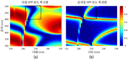
도 2 는 제1 필터를 구성하는 수직 도파로의 너비와 길이에 따른 대칭 및 반대칭 SPP 모드의 투과량을 나타낸 도면이다.
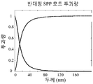
도 3 은 제2 필터의 두께에 따른 반대칭 SPP 모드의 투과량을 나타낸 도면이다.
도 4 는 제2 필터의 두께에 따른 대칭 SPP 모드의 투과량을 각각 나타낸 도면이다.
도 5 는 컨버터의 깊이와 너비에 따른 대칭 SPP 모드의 투과율을 나타낸 도면이다.
도 6 은 플라즈모닉 소자의 구조를 나타낸 도면이다.
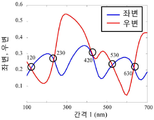
도 7 은 간격 1 을 변화시킴에 따라서 식 2 의 좌변과 우변의 변화를 나타낸 도면이다.
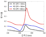
도 8 은 간격 1 을 결정하고, 간격 2 를 변화시킴에 따라서 플라즈몬 소자의 반대칭 SPP 모드의 반사율의 변화를 나타낸 도면이다.
도 9 는 플라즈모닉 소자의 자기장 세기 분포를 도시한 도면이다.1 is a conceptual diagram showing the entire structure of a plasmonic device according to the present invention.
FIG. 2 is a view showing the transmission amounts of the symmetric and anti-symmetric SPP modes according to the width and length of the vertical waveguide constituting the first filter.
Fig. 3 is a diagram showing the transmission amount of the opposite-SPP mode depending on the thickness of the second filter.
4 is a view showing the transmission amount of the symmetric SPP mode according to the thickness of the second filter, respectively.
5 is a graph showing the transmittance of the symmetric SPP mode according to the depth and width of the converter.
6 is a diagram showing a structure of a plasmonic element.
7 is a diagram showing changes in the left side and the right side of Equation 2 as the
8 is a diagram showing a variation of the reflectance in the opposite-SPP mode of the plasmon element by determining the
9 is a diagram showing a magnetic field intensity distribution of a plasmonic element.
이하, 첨부된 도면을 참조하여, 본 발명에 따른 바람직한 실시예에 대하여 설명한다. 본 실시예는 제한적인 것으로 의도된 것이 아니다.Hereinafter, preferred embodiments of the present invention will be described with reference to the accompanying drawings. The present embodiments are not intended to be limiting.
아래에서는 첨부한 도면을 참고로 하여 본 발명의 실시 예에 대하여 본 발명이 속하는 기술 분야에서 통상의 지식을 가진 자가 용이하게 실시할 수 있도록 상세히 설명한다. 그러나 본 발명은 여러 가지 상이한 형태로 구현될 수 있으며 여기에서 설명하는 실시 예에 한정되지 않는다. 그리고 도면에서 본 발명을 명확하게 설명하기 위해서 설명과 관계없는 부분은 생략하였으며, 명세서 전체를 통하여 유사한 부분에 대해서는 유사한 도면 부호를 붙였다.Hereinafter, embodiments of the present invention will be described in detail with reference to the accompanying drawings so that those skilled in the art can easily carry out the present invention. The present invention may, however, be embodied in many different forms and should not be construed as limited to the embodiments set forth herein. In order to clearly illustrate the present invention, parts not related to the description are omitted, and similar parts are denoted by like reference characters throughout the specification.
명세서 전체에서, 어떤 부분이 어떤 구성요소를 "포함"한다고 할 때, 이는 특별히 반대되는 기재가 없는 한 다른 구성요소를 제외하는 것이 아니라 다른 구성요소를 더 포함할 수 있는 것을 의미한다.Throughout the specification, when an element is referred to as "comprising ", it means that it can include other elements as well, without excluding other elements unless specifically stated otherwise.
이하에서는 본 발명의 일 실시예에 따른 플라즈모닉 소자(1)의 구조와 함께,를 최적화 설계된 플라즈모닉 소자(1)의 제조 방법을 함께 설명한다. 본 발명에 따른 플라즈모닉 소자(1)는, 바디(100)와, 바디(100)를 관통하는 중앙 도파로(200)와, 상기 중앙 도파로(200) 상에 형성되는 제1 필터(300), 컨버터(400), 및 제2 필터(500)를 포함한다. Hereinafter, a method of manufacturing the
바디(100)는 전체적으로 금속 재질로 구성되며, 소정의 길이 및 폭을 갖는다. 이하에서는 도 1 을 참조하여, 도 1 의 가로 방향은 길이 방향으로 지칭하며, 상하 방향은 폭 방향으로 설명한다. 한편, 바람직하게는, 바디(100)는 은(Ag) 재질로 구성될 수 있다. The
중앙 도파로(200)는 바디(100)의 내부를 관통하여 바디(100)의 길이 방향으로 연장되고 소정의 폭을 갖게 구성된다. 중앙 도파로(200)는 SPP 가 전파되도록 소정의 제1 유전율 값을 갖는 유전체로 구성된다. 바람직하게는, 일 실시예에 의하면, 중앙 도파로(200)를 구성하는 유전체는 실리콘 (ε=12.15)으로 구성될 수 있으며, 그 폭은 200 nm 일 수 있다.The
중앙 도파로(200)를 통해 SPP 가 전파된다. 도 1 에서, 좌측의 A 는 반대칭 SPP 가 전파되는 것을 나타내며, 우측의 B 는 대칭 SPP 가 전파되는 것을 나타낸다.The SPP is propagated through the
제1 필터(300)는 중앙 도파로(200) 상에 형성된다. 제1 필터(300)는 최우선적으로 대칭 SPP 모드가 투과하지 못하도록 하며, 이차적으로는 반대칭 SPP 모드의 투과를 최대화하는 방향으로 최적화 설계된다. 이를 통해 대칭 SPP 모드의 반사를 차단하고 반대칭 SPP 모드가 상쇄간섭으로 제거될 확률을 높이도록 설계된다.The
바람직하게는, 제1 필터(300)는 중앙 도파로(200)의 폭 방향 양 측으로 돌출된 2 개의 수직 도파로로 이루어진 notch 필터로 설계될 수 있다. 즉, 제1 필터(300)는 중앙 도파로(200)에 대해 각각 양 측에 형성된 제1 수직 도파로(310) 및 제2 수직 도파로(320)로 구성될 수 있다. 각각의 수직 도파로는 바디(100)의 폭 방향으로 소정의 길이를 갖고, 바디(100)의 길이 방향으로 소정의 너비를 갖는다. Preferably, the
제1 필터(300)의 최적화 설계는 중앙 도파로(200)에 수직한 수직 도파로의 너비와 길이에 따라서 투과량이 달라지는 것을 이용한다. 이러한 설계는 수직 도파로의 너비와 길이를 변화시킴에 따라서 대칭 및 반대칭 SPP 모드의 투과량이 변화하는 것을 시뮬레이션하여, 대칭 SPP 모드의 투과량이 최소화되면서 반대칭 SPP 모드의 투과량이 상당량 확보되는 조건을 만족시키는 영역을 선택하는 방식으로 이루어진다. The optimized design of the
예컨대, 도 2 의 경우, 너비 240 nm, 길이 330 nm 에서 대칭 SPP 모드의 투과는 3 % 미만이며, 반대칭 SPP 모드의 투과는 70 % 가 되었다.For example, in FIG. 2, the transmission of the symmetric SPP mode is less than 3% and the transmission of the opposite SPP mode is 70% at a width of 240 nm and a length of 330 nm.
이어서, 제2 필터(500)는 반대칭 SPP 모드의 투과를 차단하고 대칭 SPP 모드는 통과하도록 설계한다. 바람직하게는, 반대칭 SPP 모드의 투과를 완전히 차단하고, 대칭 SPP 모드는 완전히 통과하도록 설계됨이 바람직하다. 따라서, 반대칭 SPP 모드의 투과를 차단하고 설계를 단순화하도록 한다.Then, the
제2 필터(500)는 제1 유전체로 구성되는 중앙 도파로(200)의 일 구간을 다른 부분과 상이한 유전율을 갖는 제2 유전체 재질로 치환하여, 반대칭 SPP 모드가 특정 주파수 아래에서 컷오프(cutoff) 되는 현상을 이용한다. 제2 필터(500)를 구성하는 제2 유전체의 유전율이 높을수록 컷오프되는 주파수가 낮아지게 되므로, 제2 유전체의 유전율이 작아지면 존재하던 반대칭 SPP 모드가 사라질 수 있다. The
이에 따라서, 제2 필터(500)는 반대칭 SPP 모드에 대해 장벽과 같은 역할을 하게 된다. 도 3 에 도시된 바와 같이, 장벽의 두께에 따라서 반대칭 SPP 모드의 투과율이 터널링 현상과 흡사한 경향을 보이며 감소하는 것을 확인할 수 있다. 반대칭 SPP 모드의 투과를 막기 위히 필요한 제2 필터(500)의 두께는 대략 150 nm 이상이다. 이를 편의상 임계 두께라고 한다.Accordingly, the
한편, 도 4 에 도시된 바와 같이, 대칭 SPP 모드의 투과율과 제2 필터(500)의 두께와의 관계는 Fabry-Perot 공진에 의한 진동 양상을 보인다. 도 4 에서는 제2 필터(500)의 두께가 470 nm 의 배수일 때 거의 완전한 투과가 일어나는 것을 확인할 수 있다. 4, the relationship between the transmittance of the symmetric SPP mode and the thickness of the
상기 임계 두께 이상의 두께를 갖되, 470nm 의 배수의 두께일 때 제2 필터(500)는 반대칭 SPP 모드의 투과를 차단하며 대칭 SPP 모드를 완전히 투과시킨다. 설계상 최소한의 두께를 가지는 것이 바람직하므로, 제2 필터(500)의 두께로는 470 nm 가 선택됨이 바람직하다.When the thickness is equal to or greater than the critical thickness, and the thickness is a multiple of 470 nm, the
이어서, 컨버터(400)는 공진 구조가 없는 단일 구조 기준으로 대칭 SPP 모드와 반대칭 SPP 모드간 변환 효율이 가장 높도록 설계된다. 제2 필터(500)가 대칭 SPP 모드를 완전히 투과시키도록 설계되므로 컨버터(400) 자체의 변환 효율이 높은 것이 전체 모드 변환의 효율에 더욱 기여할 수 있다.The
컨버터(400)는 중앙 도파로(200)의 폭 방향 일 측에 형성된 사각형 그루브로 구성되며, 바디(100)의 길이방향으로 소정의 너비를 갖고, 바디(100)의 폭 방향으로 소정의 깊이를 갖는다.The
컨버터(400)의 구체적인 설계는 제1 필터(300)의 설계와 유사한 방식으로 이루어질 수 있다. 즉, 반대칭 SPP 모드를 입사시키고, 컨버터(400)의 너비와 깊이를 각각 조절하였을 때 대칭 SPP 모드의 투과율이 어떻게 나타나는지 시뮬레이션 한다. 예컨대, 도 5 에 나타난 바와 같이, 너비가 200 nm 이고, 깊이가 70 nm 일 때, 효율이 43 % 로 최적화 됨을 알 수 있다.Concrete design of the
이어서, 상기 제1 필터(300)와 상기 컨버터(400) 사이의 제1 간격(M)의 크기를 결정하고, 컨버터(400)와 제2 필터(500) 사이의 제2 간격(N)의 크기를 결정한다. 제1 간격(M)과 제2 간격(N)의 크기를 결정함으로써, 플라즈모닉 소자(1) 전체의 구조에서 반대칭 SPP 모드의 반사가 제거되도록 한다. Next, the size of the first gap M between the
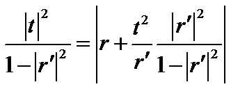
먼저, 제1 간격(M)은, 제2 간격(N)을 조절함에 따라서 반대칭 SPP 모드의 반사가 제거될 수 있는지 알려주는 조건을 이용하여 구한다. 이 조건은 플라즈모닉 소자(1) 전체의 복소반사계수를 나타내는 다음의 식 1 에 의해서 구할 수 있다.First, the first interval M is obtained by using a condition that indicates whether reflection of the opposite-SPP mode can be removed by adjusting the second interval N. [ This condition can be obtained by the following equation (1) which indicates the complex reflection coefficient of the entire plasmonic element (1).
여기에서 ![]()
![]()
![]()
![]()
![]()
![]()
![]()
![]()
![]()
![]()
![]()
![]()
![]()
![]()
아울러, ![]()
![]()
![]()
![]()
![]()
![]()
![]()
![]()
![]()
![]()
![]()
![]()
상기 식 1 의 적용은 컨버터(400), 및 제1 필터(300)의 설계와는 무관하다. 식 1 은 에너지 손실을 무시할 수 있으며, 제2 필터(500)에서 대칭 SPP 모드의 반사를 무시할 수 있는 경우 만족된다. 에너지 손실은 바람직하지 아니하므로 제1 유전체와 제2 유전체는 광을 거의 흡수하지 아니하는 물질을 사용하고, 도파로 너비 또한 반드시 필요한 만큼만 좁혀 최대한 손실을 줄이는 바, 식 1 의 적용이 가능하게 된다. The application of
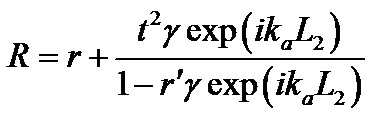
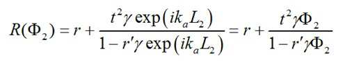
이어서, 제2 간격(N)의 크기 ![]()
![]()
![]()
![]()

식 2 는 중앙 도파로(200)에서 반대칭 SPP 의 이동간 손실이 충분히 작고, 반대칭 SPP 모드가 제2 필터(500)에서 반사되는 과정에서 에너지 손실이 크지 아니한 경우 식 1 에서 도출될 수 있다.Equation (2) can be derived from Equation (1) if the energy loss is not large in the process of the anti-nominal SPP mode transition being sufficiently small in the central waveguide (200) and the anti-symmetric SPP mode being reflected in the second filter (500).
반대칭 SPP 의 이동간 손실이 적다는 것은 수식적으로는 ![]()
![]()
![]()
![]()
![]()
![]()
또한, 제2 간격(N)의 크기 ![]()
![]()
![]()
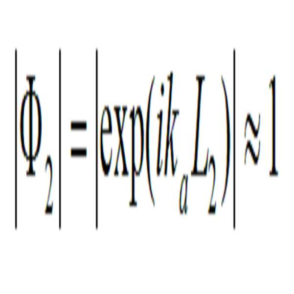
![]()
![]()
![]()
상기와 같은 전제하에, 식 2 를 얻는 과정을 설명하면 아래와 같다.Under the above premise, the process of obtaining Equation 2 will be described below.
식 1 에서, ![]()
![]()
![]()
![]()
![]()
![]()
이를 보다 상세히 설명하면, 어떠한 복소평면에 관한 식이 아래의 식 4 의 형태를 갖고, 변수의 절대값이 아래의 식 5 를 만족할 경우, (식4)의 변환에 의해, 상기 복소평면에 관한 식의 함수값은 복소평면 상에서 원의 형태로 나타난다. 이때, 상기 원의 반지름과 중심점의 위치는 아래의 식 6, 및 식 7 과 같다. 즉, 함수값은 복소평면 상에서 원의 형태로 나타나며, 상기 식의 각 계수를 통해 상기 원의 반지름과 중심점의 위치를 도출할 수 있다.More specifically, if the expression for any complex plane has the form of the following expression (4) and the absolute value of the variable satisfies the following expression (5), the expression (4) The function value appears in the form of a circle on the complex plane. At this time, the radius of the circle and the position of the center point are expressed by the following equations (6) and (7). That is, the function value appears as a circle on the complex plane, and the radius of the circle and the position of the center point can be derived through the respective coefficients of the equation.


반지름 : 
중심점 : 
한편, 상기 식 4 의 형태가 
![]()
![]()
위에서 설명한 바와 같이, 상기 식 1 에서, ![]()
![]()
![]()
![]()
또한, 
이에 따라서, 
한편, 상기 식 4, 6, 7 과 상기 식 3 의 각 항을 대응시키면 ![]()
![]()
먼저, 상기 식 4 와 상기 식 3 의 대응관계를 비교해보면 아래와 같다. First, the correspondence between Equation 4 and Equation 3 is as follows.

이에 따라서, 식 3 의 궤적을 복소평면 상에 나타낸 원의 반지름과 중심점의 위치는 아래와 같다. Accordingly, the radius of the circle and the position of the center point on the complex plane of the trajectory of Equation 3 are as follows.
반지름 : 
중심점 : 
이에 따라서, 
![]()


![]()
여기서, ![]()
![]()
![]()
![]()
![]()
![]()
![]()
![]()
여기서, 
이어서, 제1 간격(M)의 크기를 변화시켜가며 상기 식 2 의 좌변과 우변의 값을 각각 그래프로 나타내고, 좌변과 우변의 값이 같아질 때의 제1 간격(M)을 찾는다. 즉, 제1 간격(M)의 크기를 바꾸어가며 상기 식 2 를 만족시키는 제1 간격(M)의 크기를 찾는다. 상기 설명한 바와 같이, 식 2 의 변수 ![]()
![]()
![]()
![]()
![]()
![]()
이어서, 상기 과정에 따라서 도출된 제1 간격(M)의 값에 따라서 상기 변수 ![]()
![]()
![]()

![]()
![]()
![]()
도 8 을 참조하면, 식 2 의 조건을 만족시키는 제1 간격(M)의 크기의 경우에만 제2 간격(N)의 크기를 조절하여 복소반사계수 

결론적으로, 상기 식 2 를 만족하는 제1 간격(M)의 크기를 찾은 후, 제1 간격(M)을 식 1 에 대입하여 플라즈모닉 소자(1) 전체 구조의 반대칭 SPP 모드의 복소반사계수가 0 이 되는 제2 간격(N)의 크기를 찾음으로써, 플라즈모닉 소자(1) 전체의 구조에서 반대칭 SPP 모드의 반사가 제거되도록 한다.In conclusion, after finding the size of the first interval M satisfying the expression 2, the first interval M is substituted into the
실시예에 따라서, 제1 간격(M)의 크기를 120 nm 로 하고, 제2 간격(N)의 크기를 320 nm 으로 하여, 최종 변환효율이 47 % 이고, 대칭 SPP 모드 투과 이외의 성분은 모두 합하여 0.5 % 미만이 되는 구조를 갖는 플라즈몬 소자가 설계될 수 있다. 이와 같이 설계된 플라즈몬 소자에 대해 반대칭 SPP 모드를 넣는 경우의 자기장 세기 분포는 도 9 에 도시된 바와 같으며, 반사 등으로 발생하는 맥놀이 등이 매우 약해짐을 확인할 수 있다.According to the embodiment, the size of the first interval M is 120 nm, the size of the second interval N is 320 nm, the final conversion efficiency is 47%, and all components other than the transmission through the symmetric SPP mode It is possible to design a plasmon device having a structure which is less than 0.5% in total. The intensity distribution of the magnetic field when the opposite SPP mode is applied to the designed plasmon device is as shown in FIG. 9, and it can be confirmed that the beat or the like caused by reflection or the like is very weak.
본 발명에서 제안하는 구조를 갖는 플라즈모닉 소자(1)에서는 입력되는 모드에 대해 단 하나의 출력 모드만이 방출될 수 있다. 이는 부수적으로 발생된 노이즈를 제거하기 위해 필요한 각종 필터나 광 아이솔레이터 (optical isolator)의 필요성을 줄여줄 수 있으므로 광학 시스템 설계가 더 간단해 질 수 있음을 의미한다. 또한, 본 발명에 따른 구조는 극히 단순한 형태를 가지는 부분들의 조합 만으로 구성되기 때문에 형상 최적화 기법에 비해 훨씬 단순한 형태를 가지는 이점이 있다. 마지막으로 모드 변환장치가 전체적으로 공진구조이기 때문에 전체 길이가 매우 짧을 수 있어 소형화에도 유리하다.In the
이상에서는 바람직한 실시예에 대하여 도시하고 설명하였지만, 본 발명은 상술한 특정의 실시예에 한정되지 아니하며, 청구범위에서 청구하는 본 발명의 요지를 벗어남이 없이 당해 발명이 속하는 기술분야에서 통상의 지식을 가진 자에 의해 다양한 변형실시가 가능한 것은 물론이고, 이러한 변형실시들은 본 발명의 기술적 사상이나 전망으로부터 개별적으로 이해되어서는 안될 것이다.While the present invention has been particularly shown and described with reference to exemplary embodiments thereof, it is to be understood that the invention is not limited to the disclosed exemplary embodiments, but, on the contrary, It should be understood that various modifications may be made by those skilled in the art without departing from the spirit and scope of the invention.
1: 플라즈모닉 소자
100: 바디
200: 중앙 도파로
300: 제1 필터
310: 제1 수직 도파로
320: 제2 수직 도파로
400: 컨버터
500: 제2 필터1: Plasmonic element
100: Body
200: central waveguide
300: first filter
310: first vertical waveguide
320: second vertical waveguide
400: Converter
500: second filter
Claims (10)
소정의 유전율을 갖는 금속 재질로 구성된 바디;
상기 바디의 내부를 관통하여 일 방향으로 연장되게 구성되며 SPP 가 전파되는 중앙 도파로;
상기 중앙 도파로 상에 형성되는 제1 필터; 컨버터; 및 2 필터;를 포함하며,
상기 중앙 도파로는 SPP 가 전파되도록 소정의 제1 유전율 값을 갖는 제1 유전체로 구성되고,
상기 컨버터는 상기 제1 필터와 상기 제2 필터 사이에 위치하되,
상기 제1 필터는 대칭 SPP 모드의 투과를 차단하고 반대칭 SPP 모드를 통과시키며,
상기 제2 필터는 반대칭 SPP 모드의 투과를 차단하고 대칭 SPP 모드를 통과시키며,
상기 컨버터는 반대칭 SPP 모드를 대칭 SPP 모드로 변환시키는 플라즈모닉 소자.In a plasmonic device for converting an antisense SPP mode into a symmetric SPP mode and transmitting the same,
A body made of a metal material having a predetermined permittivity;
A central waveguide extending in one direction through the inside of the body and propagating SPP;
A first filter formed on the central waveguide; Converter; And a second filter,
Wherein the central waveguide is composed of a first dielectric having a predetermined first dielectric constant value so that the SPP propagates,
The converter being located between the first filter and the second filter,
Said first filter blocking transmission of a symmetric SPP mode and passing an opposite SPP mode,
The second filter intercepts the transmission of the anti-SPP mode and passes the symmetric SPP mode,
The converter converts a counter-SPP mode to a symmetric SPP mode.
상기 제1 필터는,
상기 중앙 도파로의 연장 방향에 대해 수직방향으로 소정의 길이 및 상기 중앙 도파로의 연장 방향으로 소정의 너비를 갖는 수직 도파로로 구성되되,
상기 수직 도파로는 상기 중앙 도파로의 연장 방향에 대해 양 측 수직방향으로 서로 대칭되게 연장되는 플라즈모닉 소자.The method according to claim 1,
Wherein the first filter comprises:
A vertical waveguide having a predetermined length in a direction perpendicular to the extending direction of the central waveguide and a predetermined width in a direction in which the central waveguide extends,
Wherein the vertical waveguide extends symmetrically with respect to the extending direction of the central waveguide in both vertical directions.
상기 컨버터는,
상기 중앙 도파로의 연장 방향에 대해 일 측 수직방향으로 소정의 깊이를 갖고 상기 중앙 도파로의 연장 방향으로 소정의 너비를 가지며 형성되는 그루브로 구성되는 플라즈모닉 소자.The method according to claim 1,
The converter includes:
And a groove having a predetermined depth in the one vertical direction and a predetermined width in the extending direction of the central waveguide with respect to the extending direction of the central waveguide.
상기 제2 필터는,
상기 중앙 도파로 내에 위치하며 상기 중앙 도파로의 연장 방향으로 소정의 두께를 갖고 제2 유전율 값을 갖는 제2 유전체로 구성되되,
상기 제2 유전율 값은 상기 제1 유전율 값보다 작은 플라즈모닉 소자.The method according to claim 1,
Wherein the second filter comprises:
A second dielectric having a predetermined thickness in a direction extending from the central waveguide and having a second dielectric constant,
Wherein the second permittivity value is smaller than the first permittivity value.
상기 제1 필터와 상기 컨버터는 제1 간격을 갖고 이격되게 배치되며,
상기 컨버터와 상기 제2 필터는 제2 간격을 갖고 이격되게 배치되는 플라즈모닉 소자.The method according to claim 1,
Wherein the first filter and the converter are spaced apart from each other with a first interval,
Wherein the converter and the second filter are spaced apart from each other at a second interval.
상기 제1 간격, 및 상기 제2 간격의 크기는,
상기 제1 필터에서 상기 제2 필터 방향으로 반대칭 SPP 모드가 전파될 상기 플라즈모닉 소자 전체의 반대칭 SPP 모드의 반사계수가 0 이 되도록 하는 크기를 갖는 플라즈모닉 소자.6. The method of claim 5,
The size of the first gap and the second gap,
Wherein the reflection coefficient of the opposite-SPP mode of the entire plasmonic device to be propagated in the opposite-sampling SPP mode from the first filter to the second filter is zero.
상기 바디의 내부를 관통하여 일 방향으로 연장되게 구성되며 SPP 가 전파되는 중앙 도파로;
상기 중앙 도파로 상에 형성되는 제1 필터; 컨버터; 및 2 필터;를 포함하며,
상기 중앙 도파로는 SPP 가 전파되도록 소정의 제1 유전율 값을 갖는 제1 유전체로 구성되고,
상기 컨버터는 상기 제1 필터와 상기 제2 필터 사이에 위치하되, 상기 제1 필터와 상기 컨버터는 제1 간격을 갖고 이격되게 배치되며, 상기 컨버터와 상기 제2 필터는 제2 간격을 갖고 이격되게 배치되며,
상기 제1 필터는 상기 중앙 도파로의 연장 방향에 대해 수직방향으로 소정의 길이 및 상기 중앙 도파로의 연장 방향으로 소정의 너비를 갖는 수직 도파로로 구성되되, 상기 수직 도파로는 상기 중앙 도파로의 연장 방향에 대해 양 측 수직방향으로 서로 대칭되게 연장되어 대칭 SPP 모드의 투과를 차단하고 반대칭 SPP 모드를 통과시키며,
상기 제2 필터는 상기 제1 유전율보다 작은 제2 유전율 값을 갖고 상기 중앙 도파로의 연장 방향으로 소정의 두께를 가져서 제2 유전체로 구성되어 반대칭 SPP 모드의 투과를 차단하고 대칭 SPP 모드를 통과시키며,
상기 컨버터는 상기 중앙 도파로의 연장 방향에 대해 일 측 수직방향으로 소정의 깊이를 갖고 상기 중앙 도파로의 연장 방향으로 소정의 너비를 가지며 형성되는 그루브로 구성되어 반대칭 SPP 모드를 대칭 SPP 모드로 변환시켜서,
반대칭 SPP 모드를 대칭 SPP 모드로 변환시켜 투과시키는 플라즈모닉 소자의 제조 방법으로서,
(a) 상기 제1 필터를 구성하는 수직 도파로의 길이 및 너비를 결정하는 단계;
(b) 상기 제2 필터의 두께를 결정하는 단계;
(c) 상기 컨버터의 너비 및 깊이를 결정하는 단계;
(d) 하기 수학식 1 을 만족시키는 상기 간격 1 의 값을 결정하는 단계;

(수학식 1)
(
(e) 상기 (a) 단계에서 결정된 상기 간격 1 의 값을 하기 식 2 에 대입하고, R 이 0 이 되도록 하는 상기 간격 2 의 값을 결정하는 단계;를 포함하는 플라즈모닉 소자의 제조 방법.

(수학식 2)
(
: 반대칭 SPP 모드의 전파상수
A central waveguide extending in one direction through the inside of the body and propagating SPP;
A first filter formed on the central waveguide; Converter; And a second filter,
Wherein the central waveguide is composed of a first dielectric having a predetermined first dielectric constant value so that the SPP propagates,
Wherein the converter is located between the first filter and the second filter, the first filter and the converter are spaced apart from each other with a first distance, and the converter and the second filter are spaced apart from each other by a second distance Lt; / RTI &
Wherein the first filter comprises a vertical waveguide having a predetermined length in a direction perpendicular to the extending direction of the central waveguide and a predetermined width in the extending direction of the central waveguide, Extend symmetrically with respect to each other in the vertical direction on both sides to block the transmission of the symmetric SPP mode and pass the opposite SPP mode,
The second filter has a second dielectric constant value smaller than the first dielectric constant and has a predetermined thickness in the extending direction of the central waveguide, and is formed of a second dielectric material to block the transmission of the opposite SPP mode and pass the symmetric SPP mode ,
Wherein the converter comprises a groove having a predetermined depth in a direction perpendicular to the extending direction of the central waveguide and having a predetermined width in the extending direction of the central waveguide to convert the opposite SPP mode into the symmetric SPP mode ,
A method of manufacturing a plasmonic device for converting an antisense SPP mode into a symmetric SPP mode and transmitting the same,
(a) determining a length and a width of a vertical waveguide constituting the first filter;
(b) determining a thickness of the second filter;
(c) determining the width and depth of the converter;
(d) determining a value of the interval 1 satisfying Equation (1);
(1)
(
(e) substituting the value of the interval 1 determined in the step (a) into the following equation 2, and determining the value of the interval 2 so that R becomes zero.
(2)
(
: Electromagnetic wave in SPP mode
상기 (a) 단계는,
상기 수직 도파로의 너비와 길이를 변화시킴에 따라서 대칭 및 반대칭 SPP 모드의 투과량이 변화하는 것을 시뮬레이션하여 대칭 SPP 모드의 투과량이 최소화되고 반대칭 SPP 모드의 투과량을 확보하는 영역을 선택하도록 이루어지는 플라즈모닉 소자의 제조 방법.8. The method of claim 7,
The step (a)
And the transmission amount of the symmetric SPP mode is changed by changing the width and the length of the vertical waveguide so as to minimize the transmission amount of the symmetric SPP mode and to secure the transmission amount of the opposite SPP mode, / RTI >
상기 (b) 단계는,
Fabry-Perot 공진에 의한 진동 양상을 보이는 상기 제2 필터에 대한 대칭 SPP 모드의 투과량 양상에 따라서, 상기 대칭 SPP 모드의 투과량이 최대값을 갖도록 하는 상기 제2 필터의 두께값 중에서 어느 하나이되,
반대칭SPP 모드가 컷오프되는 임계 두께 이상의 두께값 중 최소의 두께값을 상기 제2 필터의 두께로 선택하는 플라즈모닉 소자의 제조 방법.8. The method of claim 7,
The step (b)
And a thickness value of the second filter that allows the transmission amount of the symmetric SPP mode to have a maximum value in accordance with the transmission amount of the symmetric SPP mode for the second filter exhibiting a vibration mode due to Fabry-Perot resonance,
Wherein the thickness of the second filter is selected as a minimum thickness value of thickness values equal to or larger than a critical thickness at which the opposite SPP mode is cut off.
상기 (c) 단계는,
상기 컨버터의 너비와 깊이를 변화시킴에 따라서 입사된 반대칭 SPP 모드에 대한 대칭 SPP 모드의 투과율을 시뮬레이션하여 변환 효율에 따라서 상기 컨버터의 너비와 깊이를 선택하는 플라즈모닉 소자의 제조 방법.8. The method of claim 7,
The step (c)
Simulating the transmittance of the symmetric SPP mode with respect to the incident opposing SPP mode by varying the width and depth of the converter and selecting the width and depth of the converter according to the conversion efficiency.
Applications Claiming Priority (2)
| Application Number | Priority Date | Filing Date | Title |
|---|---|---|---|
| KR1020150106778 | 2015-07-28 | ||
| KR20150106778 | 2015-07-28 |
Publications (1)
| Publication Number | Publication Date |
|---|---|
| KR20170013802A true KR20170013802A (en) | 2017-02-07 |
Family
ID=58108107
Family Applications (1)
| Application Number | Title | Priority Date | Filing Date |
|---|---|---|---|
| KR1020160036323A KR20170013802A (en) | 2015-07-28 | 2016-03-25 | Plsmonic device |
Country Status (1)
| Country | Link |
|---|---|
| KR (1) | KR20170013802A (en) |
Citations (1)
| Publication number | Priority date | Publication date | Assignee | Title |
|---|---|---|---|---|
| KR970019144A (en) | 1995-09-19 | 1997-04-30 | 무라따 미치히로 | DIELECTRIC RESONATOR CAPABLE OF VARYING RESONANT FREQUENCY |
-
2016
- 2016-03-25 KR KR1020160036323A patent/KR20170013802A/en not_active Application Discontinuation
Patent Citations (1)
| Publication number | Priority date | Publication date | Assignee | Title |
|---|---|---|---|---|
| KR970019144A (en) | 1995-09-19 | 1997-04-30 | 무라따 미치히로 | DIELECTRIC RESONATOR CAPABLE OF VARYING RESONANT FREQUENCY |
Similar Documents
| Publication | Publication Date | Title |
|---|---|---|
| Özdemir et al. | Parity–time symmetry and exceptional points in photonics | |
| KR100739522B1 (en) | Electromagnetic wave frequency filter | |
| JP4398275B2 (en) | Light control element | |
| Hussein et al. | A review on the techniques for building all-optical photonic crystal logic gates | |
| Rawal et al. | Design, analysis and optimization of silicon-on-insulator photonic crystal dual band wavelength demultiplexer | |
| US7116878B2 (en) | Optical waveguide structure | |
| US9341782B2 (en) | Methods and systems for delaying optical waves | |
| Danaie et al. | Design of adjustable T-shaped and Y-shaped photonic crystal power splitters for TM and TE polarizations | |
| Xie et al. | A tunable slow light device with multiple channels based on plasmon-induced transparency | |
| Bavil et al. | A compact nanoplasmonics filter and intersection structure based on utilizing a slot cavity and a Fabry–Perot resonator | |
| Petrov et al. | Dispersion compensation with photonic crystal line-defect waveguides | |
| JP2003161971A (en) | Photonic crystal interferometric switch | |
| Ghasemi et al. | Proposal for metal–insulator–metal plasmonic power splitter and demultiplexer suitable for implementation in optical switches | |
| KR101023254B1 (en) | Plasmon transmission filter | |
| Balaji et al. | Design and analysis of waveguide taper for photonic crystal demultiplexer | |
| Mao et al. | An ARROW optical wavelength filter: design and analysis | |
| KR20170013802A (en) | Plsmonic device | |
| RU2502102C2 (en) | Optical filter | |
| JP5320566B2 (en) | Two-dimensional photonic crystal optical resonator | |
| KR101677208B1 (en) | Surface plasmon pulse group velocity converter | |
| Chung | Time-domain numerical investigation of ring resonator optical delay devices | |
| Chauhan et al. | Photonic crystal-microring resonators for tunable delay lines | |
| US7224868B2 (en) | Radiation-free optical cavity | |
| Hayran et al. | Slow light enabled wavelength demultiplexing | |
| US11520157B2 (en) | Polarization attenuator and polarization attenuation method |
Legal Events
| Date | Code | Title | Description |
|---|---|---|---|
| A201 | Request for examination | ||
| E902 | Notification of reason for refusal | ||
| E601 | Decision to refuse application |