KR20170010697A - Flexible electronic device having adhesive function and method for manufacturing same - Google Patents
Flexible electronic device having adhesive function and method for manufacturing same Download PDFInfo
- Publication number
- KR20170010697A KR20170010697A KR1020150102689A KR20150102689A KR20170010697A KR 20170010697 A KR20170010697 A KR 20170010697A KR 1020150102689 A KR1020150102689 A KR 1020150102689A KR 20150102689 A KR20150102689 A KR 20150102689A KR 20170010697 A KR20170010697 A KR 20170010697A
- Authority
- KR
- South Korea
- Prior art keywords
- electronic device
- layer
- adhesive tape
- adhesive
- flexible
- Prior art date
Links
- 239000000853 adhesive Substances 0.000 title claims abstract description 27
- 230000001070 adhesive effect Effects 0.000 title claims abstract description 27
- 238000000034 method Methods 0.000 title claims description 41
- 238000004519 manufacturing process Methods 0.000 title description 11
- 239000002390 adhesive tape Substances 0.000 claims abstract description 38
- 239000000758 substrate Substances 0.000 claims abstract description 23
- 239000012790 adhesive layer Substances 0.000 claims abstract description 12
- 239000010410 layer Substances 0.000 claims description 85
- 229910021389 graphene Inorganic materials 0.000 claims description 45
- OKTJSMMVPCPJKN-UHFFFAOYSA-N Carbon Chemical compound [C] OKTJSMMVPCPJKN-UHFFFAOYSA-N 0.000 claims description 43
- 230000005669 field effect Effects 0.000 claims description 40
- QVGXLLKOCUKJST-UHFFFAOYSA-N atomic oxygen Chemical compound [O] QVGXLLKOCUKJST-UHFFFAOYSA-N 0.000 claims description 31
- 229910052760 oxygen Inorganic materials 0.000 claims description 31
- 239000001301 oxygen Substances 0.000 claims description 31
- 238000012986 modification Methods 0.000 claims description 18
- 230000004048 modification Effects 0.000 claims description 18
- 229920001721 polyimide Polymers 0.000 claims description 16
- 239000004642 Polyimide Substances 0.000 claims description 14
- 238000009832 plasma treatment Methods 0.000 claims description 14
- 239000011248 coating agent Substances 0.000 claims description 10
- 238000000576 coating method Methods 0.000 claims description 10
- 229920003229 poly(methyl methacrylate) Polymers 0.000 claims description 9
- -1 polyethylene Polymers 0.000 claims description 9
- 239000004926 polymethyl methacrylate Substances 0.000 claims description 9
- 229920000767 polyaniline Polymers 0.000 claims description 6
- 229920000128 polypyrrole Polymers 0.000 claims description 6
- 238000012546 transfer Methods 0.000 claims description 6
- 238000005229 chemical vapour deposition Methods 0.000 claims description 5
- 239000000126 substance Substances 0.000 claims description 5
- 229920000036 polyvinylpyrrolidone Polymers 0.000 claims description 4
- ALQLPWJFHRMHIU-UHFFFAOYSA-N 1,4-diisocyanatobenzene Chemical compound O=C=NC1=CC=C(N=C=O)C=C1 ALQLPWJFHRMHIU-UHFFFAOYSA-N 0.000 claims description 3
- HPJFXFRNEJHDFR-UHFFFAOYSA-N 22291-04-9 Chemical compound C1=CC(C(N(CCN(C)C)C2=O)=O)=C3C2=CC=C2C(=O)N(CCN(C)C)C(=O)C1=C32 HPJFXFRNEJHDFR-UHFFFAOYSA-N 0.000 claims description 3
- XMWRBQBLMFGWIX-UHFFFAOYSA-N C60 fullerene Chemical compound C12=C3C(C4=C56)=C7C8=C5C5=C9C%10=C6C6=C4C1=C1C4=C6C6=C%10C%10=C9C9=C%11C5=C8C5=C8C7=C3C3=C7C2=C1C1=C2C4=C6C4=C%10C6=C9C9=C%11C5=C5C8=C3C3=C7C1=C1C2=C4C6=C2C9=C5C3=C12 XMWRBQBLMFGWIX-UHFFFAOYSA-N 0.000 claims description 3
- CBENFWSGALASAD-UHFFFAOYSA-N Ozone Chemical compound [O-][O+]=O CBENFWSGALASAD-UHFFFAOYSA-N 0.000 claims description 3
- 229920001665 Poly-4-vinylphenol Polymers 0.000 claims description 3
- 239000004698 Polyethylene Substances 0.000 claims description 3
- 239000004372 Polyvinyl alcohol Substances 0.000 claims description 3
- 238000004299 exfoliation Methods 0.000 claims description 3
- 229910003472 fullerene Inorganic materials 0.000 claims description 3
- 238000010438 heat treatment Methods 0.000 claims description 3
- RBTKNAXYKSUFRK-UHFFFAOYSA-N heliogen blue Chemical compound [Cu].[N-]1C2=C(C=CC=C3)C3=C1N=C([N-]1)C3=CC=CC=C3C1=NC([N-]1)=C(C=CC=C3)C3=C1N=C([N-]1)C3=CC=CC=C3C1=N2 RBTKNAXYKSUFRK-UHFFFAOYSA-N 0.000 claims description 3
- SLIUAWYAILUBJU-UHFFFAOYSA-N pentacene Chemical compound C1=CC=CC2=CC3=CC4=CC5=CC=CC=C5C=C4C=C3C=C21 SLIUAWYAILUBJU-UHFFFAOYSA-N 0.000 claims description 3
- KJOLVZJFMDVPGB-UHFFFAOYSA-N perylenediimide Chemical compound C=12C3=CC=C(C(NC4=O)=O)C2=C4C=CC=1C1=CC=C2C(=O)NC(=O)C4=CC=C3C1=C42 KJOLVZJFMDVPGB-UHFFFAOYSA-N 0.000 claims description 3
- 229920000301 poly(3-hexylthiophene-2,5-diyl) polymer Polymers 0.000 claims description 3
- 229920000058 polyacrylate Polymers 0.000 claims description 3
- 229920000573 polyethylene Polymers 0.000 claims description 3
- 229920002635 polyurethane Polymers 0.000 claims description 3
- 239000004814 polyurethane Substances 0.000 claims description 3
- 229920002451 polyvinyl alcohol Polymers 0.000 claims description 3
- 239000000463 material Substances 0.000 abstract description 14
- 238000005452 bending Methods 0.000 abstract description 12
- 230000003252 repetitive effect Effects 0.000 abstract description 3
- 239000010408 film Substances 0.000 description 17
- XUIMIQQOPSSXEZ-UHFFFAOYSA-N Silicon Chemical compound [Si] XUIMIQQOPSSXEZ-UHFFFAOYSA-N 0.000 description 13
- 229910052710 silicon Inorganic materials 0.000 description 13
- 239000010703 silicon Substances 0.000 description 13
- 230000000052 comparative effect Effects 0.000 description 6
- 239000004810 polytetrafluoroethylene Substances 0.000 description 6
- 229920001343 polytetrafluoroethylene Polymers 0.000 description 6
- 238000012360 testing method Methods 0.000 description 6
- 238000004458 analytical method Methods 0.000 description 5
- 239000010409 thin film Substances 0.000 description 5
- 239000005062 Polybutadiene Substances 0.000 description 4
- 239000004820 Pressure-sensitive adhesive Substances 0.000 description 4
- 229910052782 aluminium Inorganic materials 0.000 description 4
- ROOXNKNUYICQNP-UHFFFAOYSA-N ammonium persulfate Chemical compound [NH4+].[NH4+].[O-]S(=O)(=O)OOS([O-])(=O)=O ROOXNKNUYICQNP-UHFFFAOYSA-N 0.000 description 4
- 229920002857 polybutadiene Polymers 0.000 description 4
- RYGMFSIKBFXOCR-UHFFFAOYSA-N Copper Chemical compound [Cu] RYGMFSIKBFXOCR-UHFFFAOYSA-N 0.000 description 3
- 238000004833 X-ray photoelectron spectroscopy Methods 0.000 description 3
- XAGFODPZIPBFFR-UHFFFAOYSA-N aluminium Chemical compound [Al] XAGFODPZIPBFFR-UHFFFAOYSA-N 0.000 description 3
- 239000011889 copper foil Substances 0.000 description 3
- 238000005516 engineering process Methods 0.000 description 3
- 239000012212 insulator Substances 0.000 description 3
- 229920003023 plastic Polymers 0.000 description 3
- 239000004033 plastic Substances 0.000 description 3
- 239000001267 polyvinylpyrrolidone Substances 0.000 description 3
- 235000013855 polyvinylpyrrolidone Nutrition 0.000 description 3
- 238000004528 spin coating Methods 0.000 description 3
- 239000004793 Polystyrene Substances 0.000 description 2
- 229910001870 ammonium persulfate Inorganic materials 0.000 description 2
- 238000000231 atomic layer deposition Methods 0.000 description 2
- 230000005540 biological transmission Effects 0.000 description 2
- 230000015572 biosynthetic process Effects 0.000 description 2
- 238000007667 floating Methods 0.000 description 2
- 230000014509 gene expression Effects 0.000 description 2
- 229910052737 gold Inorganic materials 0.000 description 2
- 239000010931 gold Substances 0.000 description 2
- 238000005240 physical vapour deposition Methods 0.000 description 2
- 229920001610 polycaprolactone Polymers 0.000 description 2
- 239000002094 self assembled monolayer Substances 0.000 description 2
- 239000013545 self-assembled monolayer Substances 0.000 description 2
- 229910052719 titanium Inorganic materials 0.000 description 2
- 239000010936 titanium Substances 0.000 description 2
- XLYOFNOQVPJJNP-UHFFFAOYSA-N water Chemical compound O XLYOFNOQVPJJNP-UHFFFAOYSA-N 0.000 description 2
- WQYWXQCOYRZFAV-UHFFFAOYSA-N 3-octylthiophene Chemical compound CCCCCCCCC=1C=CSC=1 WQYWXQCOYRZFAV-UHFFFAOYSA-N 0.000 description 1
- IAYPIBMASNFSPL-UHFFFAOYSA-N Ethylene oxide Chemical compound C1CO1 IAYPIBMASNFSPL-UHFFFAOYSA-N 0.000 description 1
- RTAQQCXQSZGOHL-UHFFFAOYSA-N Titanium Chemical compound [Ti] RTAQQCXQSZGOHL-UHFFFAOYSA-N 0.000 description 1
- 229910052790 beryllium Inorganic materials 0.000 description 1
- 229910052797 bismuth Inorganic materials 0.000 description 1
- 239000003990 capacitor Substances 0.000 description 1
- 238000005266 casting Methods 0.000 description 1
- 230000015556 catabolic process Effects 0.000 description 1
- 229910052804 chromium Inorganic materials 0.000 description 1
- 239000000470 constituent Substances 0.000 description 1
- 229910052802 copper Inorganic materials 0.000 description 1
- 239000010949 copper Substances 0.000 description 1
- 230000003247 decreasing effect Effects 0.000 description 1
- 238000003795 desorption Methods 0.000 description 1
- 238000003618 dip coating Methods 0.000 description 1
- 239000012153 distilled water Substances 0.000 description 1
- 239000011521 glass Substances 0.000 description 1
- PCHJSUWPFVWCPO-UHFFFAOYSA-N gold Chemical compound [Au] PCHJSUWPFVWCPO-UHFFFAOYSA-N 0.000 description 1
- 229910052735 hafnium Inorganic materials 0.000 description 1
- 229910052738 indium Inorganic materials 0.000 description 1
- 238000007641 inkjet printing Methods 0.000 description 1
- 238000009413 insulation Methods 0.000 description 1
- 229910052745 lead Inorganic materials 0.000 description 1
- 239000004973 liquid crystal related substance Substances 0.000 description 1
- 229910052748 manganese Inorganic materials 0.000 description 1
- 238000005259 measurement Methods 0.000 description 1
- 238000001000 micrograph Methods 0.000 description 1
- 229910052759 nickel Inorganic materials 0.000 description 1
- 229910052758 niobium Inorganic materials 0.000 description 1
- 230000005693 optoelectronics Effects 0.000 description 1
- TWNQGVIAIRXVLR-UHFFFAOYSA-N oxo(oxoalumanyloxy)alumane Chemical compound O=[Al]O[Al]=O TWNQGVIAIRXVLR-UHFFFAOYSA-N 0.000 description 1
- 229910052763 palladium Inorganic materials 0.000 description 1
- 238000000206 photolithography Methods 0.000 description 1
- 229910052697 platinum Inorganic materials 0.000 description 1
- 229920000307 polymer substrate Polymers 0.000 description 1
- 229920001296 polysiloxane Polymers 0.000 description 1
- 229920002223 polystyrene Polymers 0.000 description 1
- 238000012545 processing Methods 0.000 description 1
- 229910052703 rhodium Inorganic materials 0.000 description 1
- 239000004065 semiconductor Substances 0.000 description 1
- 229910052709 silver Inorganic materials 0.000 description 1
- 238000007764 slot die coating Methods 0.000 description 1
- 229910052721 tungsten Inorganic materials 0.000 description 1
- 229910052720 vanadium Inorganic materials 0.000 description 1
- 229910052725 zinc Inorganic materials 0.000 description 1
- 229910052726 zirconium Inorganic materials 0.000 description 1
Images


Classifications
-
- H01L51/0097—
-
- H—ELECTRICITY
- H01—ELECTRIC ELEMENTS
- H01L—SEMICONDUCTOR DEVICES NOT COVERED BY CLASS H10
- H01L29/00—Semiconductor devices specially adapted for rectifying, amplifying, oscillating or switching and having potential barriers; Capacitors or resistors having potential barriers, e.g. a PN-junction depletion layer or carrier concentration layer; Details of semiconductor bodies or of electrodes thereof ; Multistep manufacturing processes therefor
- H01L29/66—Types of semiconductor device ; Multistep manufacturing processes therefor
- H01L29/68—Types of semiconductor device ; Multistep manufacturing processes therefor controllable by only the electric current supplied, or only the electric potential applied, to an electrode which does not carry the current to be rectified, amplified or switched
- H01L29/76—Unipolar devices, e.g. field effect transistors
- H01L29/772—Field effect transistors
- H01L29/78—Field effect transistors with field effect produced by an insulated gate
- H01L29/786—Thin film transistors, i.e. transistors with a channel being at least partly a thin film
- H01L29/78684—Thin film transistors, i.e. transistors with a channel being at least partly a thin film having a semiconductor body comprising semiconductor materials of Group IV not being silicon, or alloys including an element of the group IV, e.g. Ge, SiN alloys, SiC alloys
-
- H—ELECTRICITY
- H01—ELECTRIC ELEMENTS
- H01L—SEMICONDUCTOR DEVICES NOT COVERED BY CLASS H10
- H01L21/00—Processes or apparatus adapted for the manufacture or treatment of semiconductor or solid state devices or of parts thereof
- H01L21/02—Manufacture or treatment of semiconductor devices or of parts thereof
- H01L21/02104—Forming layers
- H01L21/02107—Forming insulating materials on a substrate
- H01L21/02225—Forming insulating materials on a substrate characterised by the process for the formation of the insulating layer
- H01L21/02227—Forming insulating materials on a substrate characterised by the process for the formation of the insulating layer formation by a process other than a deposition process
- H01L21/0223—Forming insulating materials on a substrate characterised by the process for the formation of the insulating layer formation by a process other than a deposition process formation by oxidation, e.g. oxidation of the substrate
-
- H—ELECTRICITY
- H01—ELECTRIC ELEMENTS
- H01L—SEMICONDUCTOR DEVICES NOT COVERED BY CLASS H10
- H01L21/00—Processes or apparatus adapted for the manufacture or treatment of semiconductor or solid state devices or of parts thereof
- H01L21/02—Manufacture or treatment of semiconductor devices or of parts thereof
- H01L21/02104—Forming layers
- H01L21/02365—Forming inorganic semiconducting materials on a substrate
- H01L21/02518—Deposited layers
- H01L21/02521—Materials
- H01L21/02524—Group 14 semiconducting materials
- H01L21/02527—Carbon, e.g. diamond-like carbon
-
- H—ELECTRICITY
- H01—ELECTRIC ELEMENTS
- H01L—SEMICONDUCTOR DEVICES NOT COVERED BY CLASS H10
- H01L21/00—Processes or apparatus adapted for the manufacture or treatment of semiconductor or solid state devices or of parts thereof
- H01L21/67—Apparatus specially adapted for handling semiconductor or electric solid state devices during manufacture or treatment thereof; Apparatus specially adapted for handling wafers during manufacture or treatment of semiconductor or electric solid state devices or components ; Apparatus not specifically provided for elsewhere
- H01L21/67005—Apparatus not specifically provided for elsewhere
- H01L21/67011—Apparatus for manufacture or treatment
- H01L21/67132—Apparatus for placing on an insulating substrate, e.g. tape
-
- H—ELECTRICITY
- H01—ELECTRIC ELEMENTS
- H01L—SEMICONDUCTOR DEVICES NOT COVERED BY CLASS H10
- H01L29/00—Semiconductor devices specially adapted for rectifying, amplifying, oscillating or switching and having potential barriers; Capacitors or resistors having potential barriers, e.g. a PN-junction depletion layer or carrier concentration layer; Details of semiconductor bodies or of electrodes thereof ; Multistep manufacturing processes therefor
- H01L29/02—Semiconductor bodies ; Multistep manufacturing processes therefor
- H01L29/12—Semiconductor bodies ; Multistep manufacturing processes therefor characterised by the materials of which they are formed
- H01L29/16—Semiconductor bodies ; Multistep manufacturing processes therefor characterised by the materials of which they are formed including, apart from doping materials or other impurities, only elements of Group IV of the Periodic Table
- H01L29/1606—Graphene
-
- H—ELECTRICITY
- H01—ELECTRIC ELEMENTS
- H01L—SEMICONDUCTOR DEVICES NOT COVERED BY CLASS H10
- H01L29/00—Semiconductor devices specially adapted for rectifying, amplifying, oscillating or switching and having potential barriers; Capacitors or resistors having potential barriers, e.g. a PN-junction depletion layer or carrier concentration layer; Details of semiconductor bodies or of electrodes thereof ; Multistep manufacturing processes therefor
- H01L29/40—Electrodes ; Multistep manufacturing processes therefor
- H01L29/41—Electrodes ; Multistep manufacturing processes therefor characterised by their shape, relative sizes or dispositions
- H01L29/423—Electrodes ; Multistep manufacturing processes therefor characterised by their shape, relative sizes or dispositions not carrying the current to be rectified, amplified or switched
- H01L29/42312—Gate electrodes for field effect devices
- H01L29/42316—Gate electrodes for field effect devices for field-effect transistors
- H01L29/4232—Gate electrodes for field effect devices for field-effect transistors with insulated gate
- H01L29/42356—Disposition, e.g. buried gate electrode
-
- H—ELECTRICITY
- H01—ELECTRIC ELEMENTS
- H01L—SEMICONDUCTOR DEVICES NOT COVERED BY CLASS H10
- H01L29/00—Semiconductor devices specially adapted for rectifying, amplifying, oscillating or switching and having potential barriers; Capacitors or resistors having potential barriers, e.g. a PN-junction depletion layer or carrier concentration layer; Details of semiconductor bodies or of electrodes thereof ; Multistep manufacturing processes therefor
- H01L29/40—Electrodes ; Multistep manufacturing processes therefor
- H01L29/41—Electrodes ; Multistep manufacturing processes therefor characterised by their shape, relative sizes or dispositions
- H01L29/423—Electrodes ; Multistep manufacturing processes therefor characterised by their shape, relative sizes or dispositions not carrying the current to be rectified, amplified or switched
- H01L29/42312—Gate electrodes for field effect devices
- H01L29/42316—Gate electrodes for field effect devices for field-effect transistors
- H01L29/4232—Gate electrodes for field effect devices for field-effect transistors with insulated gate
- H01L29/42364—Gate electrodes for field effect devices for field-effect transistors with insulated gate characterised by the insulating layer, e.g. thickness or uniformity
-
- H—ELECTRICITY
- H01—ELECTRIC ELEMENTS
- H01L—SEMICONDUCTOR DEVICES NOT COVERED BY CLASS H10
- H01L29/00—Semiconductor devices specially adapted for rectifying, amplifying, oscillating or switching and having potential barriers; Capacitors or resistors having potential barriers, e.g. a PN-junction depletion layer or carrier concentration layer; Details of semiconductor bodies or of electrodes thereof ; Multistep manufacturing processes therefor
- H01L29/66—Types of semiconductor device ; Multistep manufacturing processes therefor
- H01L29/66007—Multistep manufacturing processes
- H01L29/66015—Multistep manufacturing processes of devices having a semiconductor body comprising semiconducting carbon, e.g. diamond, diamond-like carbon, graphene
- H01L29/66037—Multistep manufacturing processes of devices having a semiconductor body comprising semiconducting carbon, e.g. diamond, diamond-like carbon, graphene the devices being controllable only by the electric current supplied or the electric potential applied, to an electrode which does not carry the current to be rectified, amplified or switched, e.g. three-terminal devices
- H01L29/66045—Field-effect transistors
-
- H—ELECTRICITY
- H01—ELECTRIC ELEMENTS
- H01L—SEMICONDUCTOR DEVICES NOT COVERED BY CLASS H10
- H01L29/00—Semiconductor devices specially adapted for rectifying, amplifying, oscillating or switching and having potential barriers; Capacitors or resistors having potential barriers, e.g. a PN-junction depletion layer or carrier concentration layer; Details of semiconductor bodies or of electrodes thereof ; Multistep manufacturing processes therefor
- H01L29/66—Types of semiconductor device ; Multistep manufacturing processes therefor
- H01L29/68—Types of semiconductor device ; Multistep manufacturing processes therefor controllable by only the electric current supplied, or only the electric potential applied, to an electrode which does not carry the current to be rectified, amplified or switched
- H01L29/76—Unipolar devices, e.g. field effect transistors
- H01L29/772—Field effect transistors
- H01L29/78—Field effect transistors with field effect produced by an insulated gate
- H01L29/786—Thin film transistors, i.e. transistors with a channel being at least partly a thin film
- H01L29/78603—Thin film transistors, i.e. transistors with a channel being at least partly a thin film characterised by the insulating substrate or support
-
- H—ELECTRICITY
- H10—SEMICONDUCTOR DEVICES; ELECTRIC SOLID-STATE DEVICES NOT OTHERWISE PROVIDED FOR
- H10K—ORGANIC ELECTRIC SOLID-STATE DEVICES
- H10K10/00—Organic devices specially adapted for rectifying, amplifying, oscillating or switching; Organic capacitors or resistors having potential barriers
- H10K10/40—Organic transistors
- H10K10/46—Field-effect transistors, e.g. organic thin-film transistors [OTFT]
- H10K10/462—Insulated gate field-effect transistors [IGFETs]
- H10K10/466—Lateral bottom-gate IGFETs comprising only a single gate
-
- H—ELECTRICITY
- H10—SEMICONDUCTOR DEVICES; ELECTRIC SOLID-STATE DEVICES NOT OTHERWISE PROVIDED FOR
- H10K—ORGANIC ELECTRIC SOLID-STATE DEVICES
- H10K10/00—Organic devices specially adapted for rectifying, amplifying, oscillating or switching; Organic capacitors or resistors having potential barriers
- H10K10/40—Organic transistors
- H10K10/46—Field-effect transistors, e.g. organic thin-film transistors [OTFT]
- H10K10/462—Insulated gate field-effect transistors [IGFETs]
- H10K10/468—Insulated gate field-effect transistors [IGFETs] characterised by the gate dielectrics
-
- H—ELECTRICITY
- H10—SEMICONDUCTOR DEVICES; ELECTRIC SOLID-STATE DEVICES NOT OTHERWISE PROVIDED FOR
- H10K—ORGANIC ELECTRIC SOLID-STATE DEVICES
- H10K10/00—Organic devices specially adapted for rectifying, amplifying, oscillating or switching; Organic capacitors or resistors having potential barriers
- H10K10/40—Organic transistors
- H10K10/46—Field-effect transistors, e.g. organic thin-film transistors [OTFT]
- H10K10/462—Insulated gate field-effect transistors [IGFETs]
- H10K10/484—Insulated gate field-effect transistors [IGFETs] characterised by the channel regions
-
- H—ELECTRICITY
- H10—SEMICONDUCTOR DEVICES; ELECTRIC SOLID-STATE DEVICES NOT OTHERWISE PROVIDED FOR
- H10K—ORGANIC ELECTRIC SOLID-STATE DEVICES
- H10K77/00—Constructional details of devices covered by this subclass and not covered by groups H10K10/80, H10K30/80, H10K50/80 or H10K59/80
- H10K77/10—Substrates, e.g. flexible substrates
- H10K77/111—Flexible substrates
-
- H—ELECTRICITY
- H10—SEMICONDUCTOR DEVICES; ELECTRIC SOLID-STATE DEVICES NOT OTHERWISE PROVIDED FOR
- H10K—ORGANIC ELECTRIC SOLID-STATE DEVICES
- H10K85/00—Organic materials used in the body or electrodes of devices covered by this subclass
- H10K85/10—Organic polymers or oligomers
- H10K85/141—Organic polymers or oligomers comprising aliphatic or olefinic chains, e.g. poly N-vinylcarbazol, PVC or PTFE
- H10K85/143—Polyacetylene; Derivatives thereof
-
- H—ELECTRICITY
- H01—ELECTRIC ELEMENTS
- H01L—SEMICONDUCTOR DEVICES NOT COVERED BY CLASS H10
- H01L21/00—Processes or apparatus adapted for the manufacture or treatment of semiconductor or solid state devices or of parts thereof
- H01L21/02—Manufacture or treatment of semiconductor devices or of parts thereof
- H01L21/02104—Forming layers
- H01L21/02107—Forming insulating materials on a substrate
- H01L21/02225—Forming insulating materials on a substrate characterised by the process for the formation of the insulating layer
- H01L21/02227—Forming insulating materials on a substrate characterised by the process for the formation of the insulating layer formation by a process other than a deposition process
- H01L21/02252—Forming insulating materials on a substrate characterised by the process for the formation of the insulating layer formation by a process other than a deposition process formation by plasma treatment, e.g. plasma oxidation of the substrate
-
- Y—GENERAL TAGGING OF NEW TECHNOLOGICAL DEVELOPMENTS; GENERAL TAGGING OF CROSS-SECTIONAL TECHNOLOGIES SPANNING OVER SEVERAL SECTIONS OF THE IPC; TECHNICAL SUBJECTS COVERED BY FORMER USPC CROSS-REFERENCE ART COLLECTIONS [XRACs] AND DIGESTS
- Y02—TECHNOLOGIES OR APPLICATIONS FOR MITIGATION OR ADAPTATION AGAINST CLIMATE CHANGE
- Y02E—REDUCTION OF GREENHOUSE GAS [GHG] EMISSIONS, RELATED TO ENERGY GENERATION, TRANSMISSION OR DISTRIBUTION
- Y02E10/00—Energy generation through renewable energy sources
- Y02E10/50—Photovoltaic [PV] energy
- Y02E10/549—Organic PV cells
-
- Y—GENERAL TAGGING OF NEW TECHNOLOGICAL DEVELOPMENTS; GENERAL TAGGING OF CROSS-SECTIONAL TECHNOLOGIES SPANNING OVER SEVERAL SECTIONS OF THE IPC; TECHNICAL SUBJECTS COVERED BY FORMER USPC CROSS-REFERENCE ART COLLECTIONS [XRACs] AND DIGESTS
- Y02—TECHNOLOGIES OR APPLICATIONS FOR MITIGATION OR ADAPTATION AGAINST CLIMATE CHANGE
- Y02P—CLIMATE CHANGE MITIGATION TECHNOLOGIES IN THE PRODUCTION OR PROCESSING OF GOODS
- Y02P70/00—Climate change mitigation technologies in the production process for final industrial or consumer products
- Y02P70/50—Manufacturing or production processes characterised by the final manufactured product
Landscapes
- Engineering & Computer Science (AREA)
- Microelectronics & Electronic Packaging (AREA)
- Power Engineering (AREA)
- Physics & Mathematics (AREA)
- Condensed Matter Physics & Semiconductors (AREA)
- General Physics & Mathematics (AREA)
- Computer Hardware Design (AREA)
- Ceramic Engineering (AREA)
- Manufacturing & Machinery (AREA)
- Chemical & Material Sciences (AREA)
- Materials Engineering (AREA)
- Thin Film Transistor (AREA)
Abstract
Description
본 발명은 점착 기능을 구비한 유연 전자소자 및 그의 제조방법에 관한 것으로, 점착층을 포함하는 점착테이프 상에 유연 전자소자를 형성하여 점착 기능을 구비한 유연 전자소자를 제조하는 기술에 관한 것이다.BACKGROUND OF THE
플렉서블한 전자소자는 미래 산업에 중요한 요소 기술이 될 것으로 예상되고 있다. 예를 들어 플라스틱 기판 상에 구현된 박막 트랜지스터는 구부림이 가능한 액정 표시 소자나 최근 큰 관심을 불러일으키고 있는 전자 종이(electronic paper) 및 유기 발광 소자의 구동에도 응용이 가능하다. 특히, 최근에 개발된 전자 종이는 전압 구동으로 높은 전하 이동도와 고속 스위칭 속도가 필요치 않은 표시 소자이고, 구부림이 가능한 대면적에 적용하기 유리한 기술이므로, 유연한 기판에 제작된 박막 트랜지스터의 응용 가능성이 매우 높다.Flexible electronic devices are expected to become an important technology for future industries. For example, a thin film transistor implemented on a plastic substrate can be applied to driving a bendable liquid crystal display device or an electronic paper and an organic light emitting device which have recently attracted great interest. In particular, recently developed electronic paper is a display device that does not require high charge mobility and high switching speed due to voltage driving, and is an advantageous technology applicable to a large area where bending is possible. Therefore, application of a thin film transistor fabricated on a flexible substrate is very feasible high.
종래의 기술로서 제작된 플렉서블한 전자소자는 두께가 얇은 필름형태의 플라스틱 기판(plastic substrate)을 사용하여 무게가 가볍고 상대적으로 깨질 위험이 적다는 장점이 있지만, 구부리는 힘에 의해 소자의 파괴가 일어날 수 있고 기존의 2차원적인 평면 소자와는 구조적 호환성이 없는 문제점이 있다. 또한, 박막 트랜지스터 어레이 공정을 수행한 후 플라스틱기판으로부터 고정기판을 떼어내는 탈착 공정이 필요하므로 제조공정이 많아지고, 그에 따른 제품의 양산성도 떨어지며 이에 따른 부수적인 공정 불량의 문제가 있었다.The flexible electronic device manufactured as a conventional technology has advantages in that it uses a plastic substrate having a thin film thickness and is light in weight and relatively low in risk of breakage, but breakage of the device occurs due to the bending force And there is a problem in that it is not structurally compatible with existing two-dimensional planar elements. Further, since a desorption process is required to remove the fixed substrate from the plastic substrate after performing the thin film transistor array process, the number of manufacturing processes is increased and the mass productivity of the product is also lowered, resulting in a problem of incidental process failure.
또한, 작업복이나 다양한 물품 등 표면이 곡면으로 이루어진 소재에 전자소자를 부착할 필요가 있으며, 이 경우, 소자를 지지하는 기판이 변형되면서 소자가 손상될 수 있으며, 전자소자가 부착된 대상이 휘어지거나 구부릴 수 있는 소재인 경우 소자가 지속적으로 저항을 받으며 수명이 단축되는 문제점이 있다.In addition, it is necessary to attach an electronic element to a material having a curved surface such as a work clothes or various articles. In this case, the substrate supporting the element may be deformed and the element may be damaged. In the case of a bendable material, there is a problem that the device is continuously subjected to resistance and shortens its service life.
따라서, 반복적으로 구부리거나 휘는 힘에 상관없이 기판상이 소자의 손상이 최소화되고, 박막 트랜지스터 등 전자소자 어레이 공정 후 고정기판으로부터 쉽게 탈착이 가능하며 다양한 소재에 쉽게 부착하여 사용할 수 있는 점착성을 구비한 플렉서블한 전자소자의 개발이 필요한 실정이다.Therefore, it is possible to minimize the damage of the element on the substrate irrespective of the repeated bending or bending force, to easily attach and detach from the fixed substrate after the electronic element array process such as the thin film transistor, It is necessary to develop an electronic device.
본 발명의 목적은 상기 문제점을 해결하기 위한 것으로서 유연 전자소자가 다양한 플렉서블 소재나 굴곡면이 있는 소재의 표면에 자유롭게 점착이 가능하고, 기판의 변형이나 반복적인 휘어짐에 의해서도 전자소자의 손상을 최소화하고 성능을 오랫동안 유지할 수 있는 점착 기능을 구비한 유연 전자소자를 제공하는 데 있다. It is an object of the present invention to solve the problems described above, and it is an object of the present invention to provide a flexible electronic device capable of freely adhering to a surface of a flexible material or a material having a curved surface and minimizing damage to the electronic device by deformation or repetitive bending of the substrate And to provide a flexible electronic device having an adhesive function capable of maintaining performance for a long time.
본 발명의 일 측면에 따르면, 유연 필름, 및 상기 유연 필름의 일측면 상에 형성된 점착층을 포함하는 점착테이프; 및 상기 점착테이프의 상기 일측면의 반대측 타측면 상에 형성된 전자소자;를 포함하는 점착 기능을 구비한 유연 전자소자가 제공된다.According to one aspect of the present invention, there is provided an adhesive tape comprising: a flexible film; and an adhesive layer formed on one side of the flexible film; And an electronic element formed on the other side opposite to the one side surface of the adhesive tape.
상기 전자소자가 상기 유연 필름을 기판으로 포함할 수 있다.The electronic device may include the flexible film as a substrate.
상기 유연 전자소자가 전계효과 트랜지스터, 태양전지, 유기발광다이오드, 촉각센서, 전파 식별 태그, 전자종이, 및 바이오 센서 중에서 선택된 1종 이상일 수 있다.The flexible electronic device may be at least one selected from a field effect transistor, a solar cell, an organic light emitting diode, a tactile sensor, a radio wave identification tag, an electronic paper, and a biosensor.
상기 점착 기능을 구비한 유연 전자소자가 전계효과 트랜지스터이고, 상기 전계효과 트랜지스터가 유연 필름, 및 상기 유연 필름의 일측면 상에 형성된 점착층을 포함하는 점착테이프; 상기 점착테이프의 상기 일측면의 반대측 타측면 상에 위치하는 게이트 전극; 상기 게이트 전극 상에 위치하는 게이트 절연층; 상기 게이트 절연층 상에 위치하고, 서로 이격되어 배치되는 소스 전극 및 드레인 전극; 및 상기 게이트 절연층 상에 위치하고 상기 소스전극 및 드레인 전극을 전기적으로 연결하는 활성층;을 포함할 수 있다.Wherein the flexible electronic device having the adhesive function is a field effect transistor and the field effect transistor comprises a flexible film and an adhesive layer formed on one side of the flexible film; A gate electrode located on the other side opposite to the one side of the adhesive tape; A gate insulating layer disposed on the gate electrode; Source and drain electrodes disposed on the gate insulating layer and spaced apart from each other; And an active layer located on the gate insulating layer and electrically connecting the source electrode and the drain electrode.
상기 점착테이프는 상기 타측면 상에 상기 타측면의 표면을 평탄화하는 표면개질층을 추가로 포함할 수 있다.The adhesive tape may further include a surface modification layer on the other side surface for planarizing the surface of the other side surface.
상기 표면개질층이 폴리이미드(polyimide), 폴리아크릴레이트, 폴리우레탄, 폴리에틸렌, 폴리비닐페놀, 및 폴리비닐알콜 중에서 선택된 1종 이상을 포함할 수 있다.The surface modification layer may include at least one selected from the group consisting of polyimide, polyacrylate, polyurethane, polyethylene, polyvinyl phenol, and polyvinyl alcohol.
상기 점착테이프의 영탄성률(Young's modulus)이 상기 표면 개질층의 영탄성률(Young's modulus) 보다 작을 수 있다.The Young's modulus of the adhesive tape may be smaller than the Young's modulus of the surface modification layer.
상기 표면 개질층은 제곱평균제곱근 거칠기(Root-mean-square roughness)가 0.1 내지 1 nm 일 수 있다.The surface modification layer may have a root-mean-square roughness of 0.1 to 1 nm.
상기 게이트 절연층은 두께가 1 내지 10 nm 일 수 있다.The gate insulating layer may have a thickness of 1 to 10 nm.
상기 활성층이 그래핀, PQT-12(poly(3,3'''-didodecyl quarterthiophene)), P3HT(poly(3-hexyl thiophene)), P3BT(poly(3-butyl thiophene)), P3OT(poly(3-octyl thiophene)), PPy(polypyrrole), PANI(polyaniline), PDPP(polydiketopyrrolopyrrole), PIID(polyisoindigo), PPDI(poly(perylene diimide)), PNDI(poly(naphthalene diimide)), PEO(poly(ethylene oxide)), PCL(poly(-caprolactone)), PMMA(poly(methyl methacrylate)), PS(polystyrene), PVP (poly(vinyl pyrrolidone)), 펜타센, 루브린, 구리 프탈로시아닌 및 풀러렌 중에서 선택된 1종 이상을 포함할 수 있다.The active layer may be formed of at least one selected from the group consisting of graphene, poly (3,3'-didodecyl quarterthiophene), poly (3-hexyl thiophene), P3BT (poly (3-butyl thiophene) 3-octyl thiophene), PPy (polypyrrole), PANI (polyaniline), PDPP (polydiketopyrrolopyrrole), PIID (polyisoindigo), PPDI (poly (perylene diimide), PNDI (poly (naphthalene diimide) (PVP), pentacene, lubrin, copper phthalocyanine, and fullerene), poly (methyl methacrylate), PC (poly (methyl methacrylate) Or more.
본 발명의 다른 하나의 측면에 따르면, (a) 유연 필름, 및 상기 유연 필름의 일측면 상에 형성된 점착층을 포함하는 점착테이프를 준비하는 단계; 및 (b) 상기 점착테이프의 상기 일측면의 반대측 타측면 상에 전자소자를 형성하는 단계;를 포함하는 점착 기능을 구비한 유연 전자소자의 제조방법이 제공된다.According to another aspect of the present invention, there is provided a method of manufacturing a flexible film, comprising the steps of: (a) preparing an adhesive tape comprising a flexible film and an adhesive layer formed on one side of the flexible film; And (b) forming an electronic device on the other side opposite to the one side of the adhesive tape. The present invention also provides a method for manufacturing a flexible electronic device having an adhesive function.
상기 유연 전자소자의 제조방법이 단계 (a) 후에 상기 점착테이프의 상기 일측면의 반대측 타측면 상에 표면개질층을 코팅하는 단계를 추가로 포함할 수 있다.The method of manufacturing a flexible electronic device may further include, after step (a), coating the surface modification layer on the other opposite side of the one side of the adhesive tape.
단계 (b)의 전자소자가 전계효과 트랜지스터, 태양전지, 유기발광다이오드, 촉각센서, 전파 식별 태그, 전자종이, 및 바이오 센서 중에서 선택된 1종 이상일 수 있다.The electronic device of step (b) may be at least one selected from a field effect transistor, a solar cell, an organic light emitting diode, a tactile sensor, a radio wave identification tag, an electronic paper, and a biosensor.
단계 (b)의 전자소자가 전계효과 트랜지스터이고, 단계 (b)가, (b-1) 상기 점착테이프의 상기 일측면의 반대측 타측면 상에 게이트 전극을 형성하는 단계; (b-2) 상기 게이트 전극상에 게이트 절연층을 형성하는 단계; (b-3) 상기 게이트 절연층 상에 소스 전극 및 드레인 전극을 형성하는 단계; 및 (b-4) 상기 게이트 절연층 상에, 상기 소스 전극 및 드레인 전극을 전기적으로 연결하는 활성층을 형성하는 단계;를 포함할 수 있다.Wherein the electronic element of step (b) is a field-effect transistor, and step (b) comprises: (b-1) forming a gate electrode on the other side opposite to the one side of the adhesive tape; (b-2) forming a gate insulating layer on the gate electrode; (b-3) forming a source electrode and a drain electrode on the gate insulating layer; And (b-4) forming an active layer electrically connecting the source electrode and the drain electrode on the gate insulating layer.
단계 (b-2)가 UV 오존처리, 산소 분위기 열처리, 및 산소 플라즈마 처리 중에서 선택된 어느 하나의 방법으로 수행될 수 있다.Step (b-2) may be carried out by any one of the methods selected from UV ozone treatment, oxygen atmosphere heat treatment, and oxygen plasma treatment.
단계 (b-2)가 산소 플라즈마 처리에 의해 수행될 수 있다.Step (b-2) may be performed by oxygen plasma treatment.
상기 산소 플라즈마 처리가 10 내지 300W의 RF 전력 조건에서 수행될 수 있다.The oxygen plasma treatment may be performed at RF power conditions of 10 to 300 W.
상기 산소 플라즈마 처리가 1 내지 1000 mTorr의 압력 조건에서 수행될 수 있다.The oxygen plasma treatment may be performed at a pressure of 1 to 1000 mTorr.
상기 활성층이 그래핀층이고, 상기 그래핀층이 물리적 또는 화학적 박리에 의해 제조된 그래핀, SiC에서 성장시켜 제조된 그래핀, 및 화학기상 증착법에 의해 제조된 그래핀 중에서 선택된 어느 하나일 수 있다.The active layer may be a graphene layer, and the graphene layer may be any of graphene produced by physical or chemical exfoliation, graphene grown by growing in SiC, and graphene produced by chemical vapor deposition.
단계 (b-4)가 건식 전사법에 따라 수행될 수 있다.Step (b-4) can be carried out according to a dry transfer method.
본 발명의 유연 전자소자는 다양한 플렉서블 소재나 굴곡면이 있는 소재의 표면에 자유롭게 점착이 가능하고, 기판의 변형이나 반복적인 밴딩(bending)에 의해서도 전자소자의 손상을 최소화하고 성능을 오랫동안 유지할 수 있는 효과가 있다.The flexible electronic device of the present invention can be freely adhered to the surface of various flexible materials or materials having curved surfaces and can minimize the damage of electronic devices and maintain the performance for a long time due to deformation or repetitive bending of the substrate It is effective.
도 1은 본 발명의 점착 기능을 구비한 유연 전자소자의 제조방법을 순차적으로 나타낸 흐름도이다.
도 2는 실시예 1에 따라 실리콘 웨이퍼 상에 제조된 점착 기능을 구비한 유연 전자소자의 개략도 및 측단면도(a) 및 실리콘 웨이퍼에서 분리한 점착 기능을 구비한 유연 전자소자의 사진(b)을 나타낸 것이다.
도3은 스카치 테이프 표면에 폴리이미드의 코팅 전 후 거칠기를 비교한 AFM(atomic force microscope) 이미지이다.
도 4는 실시예 1에 의해 제조된 그래핀 전계효과 트랜지스터를 지폐, 실리콘 웨이퍼, 종이에 부착한 이미지 및 각각의 전기적 성능을 분석하여 나타낸 그래프이다.
도 5는 실시예 1 내지 3에 의해 제조된 게이트절연층의 누설전류밀도(current density)를 측정하여 나타낸 그래프이다.
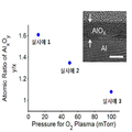
도 6은 실시예 1 내지 3에 의해 제조된 그래핀 전계효과 트랜지스터의 산소 플라즈마 압력에 따른 AlOX의 원자비를 측정하여 나타낸 그래프 및 및 TEM(transmission electron microscope) 이미지이다.
도 7은 실시예 1에 따라 제조된 게이트절연층/게이트 패턴/폴리이미드/접착테이프가 오피스 페이퍼(office paper)에 부착된 게이트절연층/게이트 패턴/폴리이미드/접착테이프/오피스 페이퍼(a)의 측단면 및 비교예 1에 따라 제조된 게이트 절연층/게이트 패턴/폴리이미드(b)의 측단면을 나타낸 것이다.
도 8은 도 7의 두 샘플에 대한 구부림 곡률반경(bending radius)에 따른 표면 변형률(surface strain)을 측정하여 나타낸 것이다. 1 is a flowchart sequentially illustrating a method of manufacturing a flexible electronic device having an adhesive function according to the present invention.
Fig. 2 is a schematic view and cross-sectional side view (a) of a flexible electronic device having an adhesive function manufactured on a silicon wafer according to Example 1 and a photograph (b) of a flexible electronic device having an adhesive function separated from a silicon wafer .
3 is an AFM (atomic force microscope) image obtained by comparing the roughness of the surface of the scotch tape before and after coating the polyimide.
FIG. 4 is a graph showing an image obtained by attaching a graphene field effect transistor fabricated according to Example 1 to a banknote, a silicon wafer, paper, and the electrical performance of each.
FIG. 5 is a graph showing leakage current density measured by the gate insulating layers manufactured in Examples 1 to 3. FIG.
FIG. 6 is a graph and TEM (transmission electron microscope) image showing the atomic ratio of AlO x according to the oxygen plasma pressure of the graphene field effect transistor manufactured in Examples 1 to 3.
FIG. 7 is a cross-sectional view of the gate insulating layer / gate pattern / polyimide / adhesive tape / office paper (a) prepared according to Example 1, the gate insulating layer / gate pattern / polyimide / adhesive tape adhered to office paper, And a cross-sectional view of the gate insulating layer / gate pattern / polyimide (b) prepared according to Comparative Example 1.
FIG. 8 is a graph showing the measured surface strain according to the bending radius for the two samples in FIG. 7. FIG.
이하, 본 발명이 속하는 기술 분야에서 통상의 지식을 가진 자가 용이하게 실시할 수 있도록 본 발명의 구현예 및 실시예를 상세히 설명한다. Hereinafter, embodiments and examples of the present invention will be described in detail so that those skilled in the art can easily carry out the present invention.
본원에서 사용한 용어는 단지 특정한 실시예를 설명하기 위해 사용된 것으로, 본 발명을 한정하려는 의도가 아니다. 이하의 설명은 본 발명을 특정한 실시 형태에 대해 한정하려는 것이 아니며, 본 발명의 사상 및 기술 범위에 포함되는 모든 변환, 균등물 내지 대체물을 포함하는 것으로 이해되어야 한다. 본 발명을 설명함에 있어서 관련된 공지 기술에 대한 구체적인 설명이 본 발명의 요지를 흐릴 수 있다고 판단되는 경우 그 상세한 설명을 생략한다.The terminology used herein is for the purpose of describing particular embodiments only and is not intended to be limiting of the invention. It is to be understood that the following description is not intended to limit the invention to specific embodiments but includes all modifications, equivalents, and alternatives falling within the spirit and scope of the invention. DETAILED DESCRIPTION OF THE PREFERRED EMBODIMENTS Hereinafter, the present invention will be described in detail with reference to the accompanying drawings.
또한, 이하에서 사용될 제1, 제2 등과 같이 서수를 포함하는 용어는 다양한 구성요소들을 설명하는데 사용될 수 있지만, 상기 구성요소들은 상기 용어들에 의해 한정되지는 않는다. 상기 용어들은 하나의 구성요소를 다른 구성요소로부터 구별하는 목적으로만 사용된다. 예를 들어, 본 발명의 권리 범위를 벗어나지 않으면서 제1 구성요소는 제2 구성요소로 명명될 수 있고, 유사하게 제2 구성요소도 제1 구성요소로 명명될 수 있다.Furthermore, terms including an ordinal number such as first, second, etc. to be used below can be used to describe various elements, but the constituent elements are not limited by the terms. The terms are used only for the purpose of distinguishing one component from another. For example, without departing from the scope of the present invention, the first component may be referred to as a second component, and similarly, the second component may also be referred to as a first component.
또한, 어떤 구성요소가 다른 구성요소 상에 "형성되어" 있다거나 "적층되어" 있다는 의미로 언급된 때에는, 그 다른 구성요소의 표면 상의 전면 또는 일면에 직접 부착되어 형성되어 있거나 적층되어 있을 수도 있지만, 중간에 다른 구성요소가 더 존재할 수도 있다고 이해되어야 할 것이다.Also, when an element is referred to in the sense of being "formed" or "laminated" on another element, it may be directly attached or formed on the front surface or one surface of the surface of the other element , It should be understood that there may be other components in between.
또한 단수의 표현은 문맥상 명백하게 다르게 뜻하지 않는 한, 복수의 표현을 포함한다. 본 출원에서, "포함하다" 또는 "가지다" 등의 용어는 명세서상에 기재된 특징, 숫자, 단계, 동작, 구성요소, 또는 이들을 조합한 것이 존재함을 지정하려는 것이지, 하나 또는 그 이상의 다른 특징들이나 숫자, 단계, 동작, 구성요소, 또는 이들을 조합한 것들의 존재 또는 부가 가능성을 미리 배제하지 않는 것으로 이해되어야 한다.Also, the singular expressions include plural expressions unless the context clearly dictates otherwise. In the present application, the terms "comprises ", or" having ", and the like, specify that the presence of stated features, integers, steps, operations, elements, or combinations thereof, But do not preclude the presence or addition of one or more other features, integers, steps, operations, elements, or combinations thereof.
이하, 본 발명의 점착 기능을 구비한 유연 전자소자를 설명하도록 한다.Hereinafter, a flexible electronic device having the adhesive function of the present invention will be described.
본 발명의 점착기능을 구비한 유연 전자소자는, 유연 필름, 및 상기 유연 필름의 일측면 상에 형성된 점착층을 포함하는 점착테이프; 및 상기 점착테이프의 상기 일측면의 반대측 타측면 상에 형성된 전자소자;를 포함할 수 있다.The flexible electronic device having the adhesive function of the present invention comprises: a pressure-sensitive adhesive tape comprising a flexible film and an adhesive layer formed on one side of the flexible film; And an electronic device formed on the other side opposite to the one side of the adhesive tape.
상기 전자소자는 상기 유연 필름을 기판으로 포함할 수 있다.The electronic device may include the flexible film as a substrate.
상기 전자소자는 전계효과 트랜지스터, 태양전지, 유기발광다이오드, 촉각센서, 전파 식별 태그, 전자종이, 바이오 센서 등일 수 있다.The electronic device may be a field effect transistor, a solar cell, an organic light emitting diode, a tactile sensor, a radio wave identification tag, an electronic paper, a biosensor, or the like.
상기 점착 기능을 구비한 유연 전자소자는, 유연 필름, 및 상기 유연 필름의 일측면 상에 형성된 점착층을 포함하는 점착테이프; 상기 점착테이프의 상기 일측면의 반대측 타측면 상에 위치하는 게이트 전극; 상기 게이트 전극 상에 위치하는 게이트 절연층; 상기 게이트 절연층 상에 위치하고, 서로 이격되어 배치되는 소스 전극 및 드레인 전극; 및 상기 게이트 절연층 상에 위치하고 상기 소스전극 및 드레인 전극을 전기적으로 연결하는 활성층;을 포함하는 전계효과 트랜지스터일 수 있다.Wherein the flexible electronic device having the adhesive function comprises: a pressure-sensitive adhesive tape comprising a flexible film and an adhesive layer formed on one side of the flexible film; A gate electrode located on the other side opposite to the one side of the adhesive tape; A gate insulating layer disposed on the gate electrode; Source and drain electrodes disposed on the gate insulating layer and spaced apart from each other; And an active layer located on the gate insulating layer and electrically connecting the source electrode and the drain electrode.
상기 점착테이프의 상기 타측면 상에 상기 타측면의 표면을 평탄화하는 표면개질층을 추가로 포함할 수 있다.And a surface modification layer for planarizing the surface of the other side surface on the other side surface of the adhesive tape.
상기 표면개질층은 폴리이미드(polyimide), 폴리아크릴레이트, 폴리우레탄, 폴리에틸렌, 폴리비닐페놀, 폴리비닐알콜 등일 수 있다. 바람직하게는 폴리이미드(polyimide)일 수 있다.The surface modification layer may be polyimide, polyacrylate, polyurethane, polyethylene, polyvinyl phenol, polyvinyl alcohol, or the like. Preferably, it may be a polyimide.
상기 점착테이프의 영탄성률(Young's modulus)이 상기 표면 개질층의 영탄성률(Young's modulus) 보다 작을 수 있다.The Young's modulus of the adhesive tape may be smaller than the Young's modulus of the surface modification layer.
바람직하게는, 상기 점착테이프의 영탄성률(Young's modulus)은 0.1 내지 100 MPa인 것이 바람직하고, 더욱 바람직하게는 1 내지 10 Mpa일 수 있다.Preferably, the Young's modulus of the adhesive tape is 0.1 to 100 MPa, and more preferably 1 to 10 MPa.
또한, 상기 표면 개질층의 영탄성률(Young's modulus)은 상기 점착테이프의 영탄성률(Young's modulus)에 비해 상대적으로 큰 것이 바람직하고, 0.1 내지 100 GPa일 수 있고, 더 바람직하게는 1 내지 10 GPa일 수 있다.Also, the Young's modulus of the surface modifying layer is preferably relatively large compared to Young's modulus of the adhesive tape, may be 0.1 to 100 GPa, more preferably 1 to 10 GPa .
상기 점착테이프 표면의 제곱평균제곱근 거칠기(Root-mean-square roughness)는 10 내지 100 nm인 것이 바람직하고, 더욱 바람직하게는 20 내지 80 nm일 수 있다.The root mean square roughness of the adhesive tape surface is preferably 10 to 100 nm, more preferably 20 to 80 nm.
상기 표면 개질층은 두께가 1 내지 20㎛인 것이 바람직하고, 더욱 바람직하게는 5 내지 15㎛일 수 있다.The thickness of the surface modification layer is preferably 1 to 20 占 퐉, more preferably 5 to 15 占 퐉.
상기 표면 개질층은 제곱평균제곱근 거칠기(Root-mean-square roughness)가 0.1 내지 1 nm인 것이 바람직하고, 더욱 바람직하게는 0.1 내지 0.4 nm일 수 있다.The surface modification layer preferably has a root-mean-square roughness of 0.1 to 1 nm, more preferably 0.1 to 0.4 nm.
상기 게이트 절연층은 두께가 1 내지 10 nm인 것이 바람직하고, 더욱 바람직하게는 3 내지 7 nm 일 수 있다. The thickness of the gate insulating layer is preferably 1 to 10 nm, more preferably 3 to 7 nm.
상기 소스 전극 및 드레인 전극은 Au, Al, Ag, Be, Bi, Co, Cu, Cr, Hf, In, Mn, Mo, Mg, Ni, Nb, Pb, Pd, Pt, Rh, Re, Ru, Sb, Ta, Te, Ti, V, W, Zr, Zn 등을 적용할 수 있다.The source electrode and the drain electrode may be formed of one selected from the group consisting of Au, Al, Ag, Be, Bi, Co, Cu, Cr, Hf, In, Mn, Mo, Mg, Ni, Nb, Pb, Pd, Pt, Rh, , Ta, Te, Ti, V, W, Zr, and Zn.
상기 유기 활성층은 그래핀, PQT-12(poly(3,3'''-didodecyl quarterthiophene)), P3HT(poly(3-hexyl thiophene)), P3BT(poly(3-butyl thiophene)), P3OT(poly(3-octyl thiophene)), PPy(polypyrrole), PANI(polyaniline), PDPP(polydiketopyrrolopyrrole), PIID(polyisoindigo), PPDI(poly(perylene diimide)), PNDI(poly(naphthalene diimide)), PEO(poly(ethylene oxide)), PCL(poly(-caprolactone)), PMMA(poly(methyl methacrylate)), PS(polystyrene), PVP (poly(vinyl pyrrolidone)), 펜타센, 루브린, 구리 프탈로시아닌 및 풀러렌 등일 수 있다.The organic active layer may include at least one selected from the group consisting of graphene, poly (3,3'-didodecyl quarterthiophene), poly (3-hexyl thiophene), P3BT 3-octyl thiophene), PPy (polypyrrole), PANI (polyaniline), PDPP (polydiketopyrrolopyrrole), PIID (polyisoindigo), PPDI (poly (perylene diimide), PNDI (poly (naphthalene diimide) ethylene oxide (PCL), poly (caprolactone), poly (methyl methacrylate), PS (polystyrene), polyvinyl pyrrolidone (PVP), pentacene, lubrin, copper phthalocyanine and fullerene .
본 발명의 유연 전자소자는 다양한 플렉서블 소재나 굴곡면이 있는 소재의 표면에 부착될 수 있다. 예를 들면, 상기 플렉서블 소재가 펜, 피부, 지폐, 의류, 유리 등일 수 있다.The flexible electronic device of the present invention can be attached to the surface of a material having various flexible materials or curved surfaces. For example, the flexible material may be a pen, skin, banknote, clothing, glass, or the like.
도 1은 본 발명의 점착 기능을 구비한 유연 전자소자의 제조방법을 순차적으로 나타낸 흐름도이다. 이하, 도 1을 참조하여 본 발명의 점착 기능을 구비한 유연 전자소자의 제조방법을 설명하도록 한다.1 is a flowchart sequentially illustrating a method of manufacturing a flexible electronic device having an adhesive function according to the present invention. Hereinafter, a method of manufacturing a flexible electronic device having an adhesive function of the present invention will be described with reference to FIG.
먼저, 유연 필름, 및 상기 유연 필름의 일측면 상에 형성된 점착층을 포함하는 점착테이프를 준비한다(단계 a).First, an adhesive tape comprising a flexible film and an adhesive layer formed on one side of the flexible film is prepared (step a).
상기 점착테이프의 상기 일측면의 반대측 타측면 상에 표면개질층을 추가로 코팅하는 단계를 포함할 수 있다.And further coating a surface modification layer on the other opposite side of the one side of the adhesive tape.
상기 코팅이 물리적 기상증착, 화학적 기상증착, 스핀코팅, 잉크젯 프린팅, 딥 코팅, 드롭 캐스팅, 바 코팅, 슬롯다이 코팅 등일 수 있다. 바람직하게는 스핀코팅일 수 있다.The coating can be physical vapor deposition, chemical vapor deposition, spin coating, inkjet printing, dip coating, drop casting, bar coating, slot die coating, and the like. Preferably a spin coating.
상기 코팅하는 단계 이후, 가열하여 건조시킬 수 있다.After the coating step, it may be heated and dried.
이후, 상기 점착테이프의 상기 일측면의 반대측 타측면 상에 전자소자를 형성한다(단계 b).Thereafter, an electronic device is formed on the other side opposite to the one side of the adhesive tape (step b).
상기 전자소자는 전계효과 트랜지스터, 태양전지, 유기발광다이오드, 촉각센서, 전파 식별 태그, 전자종이, 바이오 센서 등 다양한 전자소자가 적용될 수 있으나, 이하에서는 예시적으로 전계효과 트랜지스터를 형성하는 방법에 대해 설명하도록 한다.Various electronic devices such as a field effect transistor, a solar cell, an organic light emitting diode, a tactile sensor, a radio wave identification tag, an electronic paper, and a biosensor may be used as the electronic device. Hereinafter, a method of forming a field effect transistor Explain it.
구체적으로, 상기 점착테이프의 상기 일측면의 반대측 타측면 상에 게이트 전극을 형성한다(단계 b-1).Specifically, a gate electrode is formed on the other side opposite to the one side of the adhesive tape (step b-1).
b-1 단계는 쉐도우 마스크, 포토리소그래피, 물리적기상증착법, 화학적 기상증착법, 스핀코팅 등에 의해 수행될 수 있다.Step b-1 may be performed by a shadow mask, photolithography, physical vapor deposition, chemical vapor deposition, spin coating, or the like.
다음으로, 상기 게이트 전극 상에 게이트 절연층을 형성한다(단계 b-2).Next, a gate insulating layer is formed on the gate electrode (step b-2).
b-2 단계는 UV 오존처리, 산소 분위기 열처리, 산소 플라즈마 처리 등에 의해 수행되는 것이 바람직하고, 더욱 바람직하게는 산소 플라즈마 처리에 의해 수행될 수 있다.Step b-2 is preferably performed by UV ozone treatment, oxygen atmosphere heat treatment, oxygen plasma treatment or the like, and more preferably by oxygen plasma treatment.
종래의 고분자 기판에 비해 본 발명에 적용되는 점착테이프는 열이나 화학물질에 매우 취약하므로, 고온이나 고압이 요구되는 공정에서 손상될 수 있다. 따라서, 온도가 낮고, 화학물질에 노출되지 않는 마일드한 공정으로 게이트 절연층을 형성할 필요가 있다. Compared to the conventional polymer substrate, the adhesive tape applied to the present invention is very vulnerable to heat or chemical substances and can be damaged in a process requiring high temperature or high pressure. Therefore, it is necessary to form the gate insulating layer with a mild process in which the temperature is low and is not exposed to chemical substances.
상기 산소 플라즈마 처리는 바람직하게는 10 내지 300W, 더욱 바람직하게는 200 내지 280W의 RF 전력(Radio Frequency Power) 조건에서 수행할 수 있다.The oxygen plasma treatment may preferably be performed under RF power conditions of 10 to 300 W, more preferably 200 to 280 W.
또한, 상기 산소 플라즈마 처리 시간은 상기 전력 조건에서 1 내지 20분 동안 수행되는 것이 바람직하고, 더욱 바람직하게는 5 내지 15 분 동안 수행될 수 있다.Further, the oxygen plasma treatment time is preferably 1 to 20 minutes, more preferably 5 to 15 minutes in the power condition.
또한, 상기 산소 플라즈마의 압력 조건은 바람직하게는 1 내지 1000 mTorr, 더욱 바람직하게는 10 내지 100 mTorr일 수 있다.Further, the pressure condition of the oxygen plasma may preferably be 1 to 1000 mTorr, more preferably 10 to 100 mTorr.
다음으로, 상기 게이트 절연층 상에 소스 전극 및 드레인 전극을 형성한다(단계 b-3).Next, a source electrode and a drain electrode are formed on the gate insulating layer (step b-3).
상기 소스 전극 및 드레인 전극의 재료는 상기 점착 기능을 구비한 유연 전자 소자의 설명에 기재된 바와 동일하므로 상세한 내용은 그 부분을 참조하기로 한다.The materials of the source electrode and the drain electrode are the same as those described in the description of the flexible electronic device having the adhesive function, and therefore, the details thereof will be referred to.
마지막으로, 상기 게이트 절연층 상에, 상기 소스 전극 및 드레인 전극을 전기적으로 연결하는 활성층을 형성한다(단계 b-4).Finally, an active layer for electrically connecting the source electrode and the drain electrode is formed on the gate insulating layer (step b-4).
상기 활성층의 종류는 상술한 점착 기능을 구비한 유연 전자소자에서 설명한 바와 동일하므로 구체적인 내용은 그 부분을 참조하기로 한다.Since the kind of the active layer is the same as that described in the above-described flexible electronic device having the adhesive function, the detailed contents will be referred to.
상기 활성층은 다양한 반도체 물질을 적용할 수 있으나, 바람직하게는 그래핀을 포함하는 그래핀층을 적용할 수 있다. Various semiconductor materials can be used for the active layer, but a graphene layer including graphene may be preferably used.
상기 그래핀층은 물리적 또는 화학적 박리에 의해 제조된 그래핀, SiC에서 성장시켜 제조된 그래핀, 화학기상 증착법에 의해 제조된 그래핀 등일 수 있다.The graphene layer may be graphene produced by physical or chemical exfoliation, graphene grown by SiC, graphene produced by chemical vapor deposition, or the like.
상기 그래핀층의 형성은 상기 게이트 절연층상에 그래핀을 건식 전사법에 따라 수행하는 것이 바람직하다. 왜냐하면, 본 발명에 적용되는 점착테이프는 습기에 취약하므로 종래 사용되는 습식 전사법에 비해 건식 전사법을 사용하는 것이 더욱 바람직하다.The formation of the graphene layer is preferably performed by a dry transfer method on the gate insulating layer. This is because the adhesive tape applied to the present invention is vulnerable to moisture, and therefore, it is more preferable to use the dry transfer method as compared with the wet transfer method used in the past.
이하, 본 발명의 바람직한 실시예를 들어 설명하도록 한다.Hereinafter, preferred embodiments of the present invention will be described.
[실시예][Example]
실시예Example 1 One
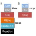
유연필름으로 폴리테트라 플루오로에틸렌(PTFE, Polytetrafluoroethylene)과 점착층으로 실리콘계 점착제를 포함하는 점착 테이프인 스카치 테이프(3MTM, 5480, PTFE 두께 50㎛, 실리콘계 접착제 두께 44㎛)를 준비하였다. 상기 스카치 테이프를 실리콘 웨이퍼 상에 부착하였다. Scotch tape (3M ™, 5480, PTFE thickness: 50 μm, silicon-based adhesive thickness: 44 μm) which is an adhesive tape containing a silicone-based adhesive as an adhesive layer was prepared as a flexible film and PTFE (Polytetrafluoroethylene). The scotch tape was mounted on a silicon wafer.
다음으로, 상기 실리콘 웨이퍼 상에 부착된 테이프상에 폴리이미드 용액(VTECTM, PI-1388)을 3000rpm으로 30초 동안 스핀코팅하고, 60℃ 및 150℃에서 순차적으로 10분 동안 베이킹(baking)하여 폴리이미드 표면개질층을 형성하였다. Next, a polyimide solution (VTEC TM , PI-1388) was spin coated on the tape adhered on the silicon wafer at 3000 rpm for 30 seconds and baked at 60 캜 and 150 캜 for 10 minutes successively Thereby forming a polyimide surface modification layer.
다음으로, 상기 표면개질층상에 게이트 전극으로 알루미늄 층(30nm)을 섀도우 마스크를 이용하여 열 증착기 안에서 열증착하였다. Next, an aluminum layer (30 nm) as a gate electrode was thermally deposited on the surface modification layer in a thermal evaporator using a shadow mask.
이후, 상기 알루미늄 층을 250W의 RF 전력(radio frequency power) 조건에서 7분 동안 산소 플라즈마 챔버에서 산화시켜 상기 알루미늄 층의 표면에 게이트 절연층을 형성하였다. 플라즈마 처리를 하는 동안, 산소 압력은 플라즈마가 존재하는 동안 가능한 가장 낮은 수준으로 유지하였다. 이때, 플라즈마 챔버의 가장 낮은 압력 수준은 12mTorr 였다. Thereafter, the aluminum layer was oxidized in an oxygen plasma chamber for 7 minutes under RF power of 250 W to form a gate insulating layer on the surface of the aluminum layer. During the plasma treatment, the oxygen pressure was kept to the lowest possible level during the presence of the plasma. At this time, the lowest pressure level of the plasma chamber was 12 mTorr.
다음으로, 상기 게이트 절연층상에 소스 및 드레인 전극(5nm 두께의 티타늄상에 40nm 두께 금)을 섀도우 마스크를 이용하여 열층착하였다.Next, source and drain electrodes (5 nm thick titanium and 40 nm thick gold) were thermally deposited on the gate insulating layer using a shadow mask.
마지막으로, 상기 소스 및 드레인 전극을 전기적으로 연결하도록 상기 게이트 유전체층 상에 건식 전사법에 따라 그래핀 활성층을 형성하였다. 구체적으로, 구리 포일 위에 성장된 그래핀 상에 폴리부타디엔과 PMMA를 차례로 코팅하여 바이레이어 지지층을 형성하고, 코팅면의 반대편에 존재하는 그래핀은 산소 플라즈마를 통해 제거한 후, 0.1M의 과황산암모늄 수용액에 넣어 구리 포일을 에칭하였다. 구리 포일이 다 에칭된 후에 상기 과황산암모늄 수용액에 떠있는 PMMA/폴리부타디엔/그래핀층을 증류수 배스에 옮긴 후, 물에 떠있는 PMMA/폴리부타디엔/그래핀층을 구멍이 뚫린 샘플 홀더에 고정시키고 건조시켰다. 다음으로, 상기 홀더에 고정된 상기 폴리부타디엔/PMMA/그래핀층을 상기 소스 및 드레인 전극, 게이트 절연층과 접촉시키고 열과 압력을 가하여 그래핀을 건식 전사함으로써 그래핀 활성층을 형성하여 그래핀 전계효과 트랜지스터를 제조하였다.Finally, a graphene active layer was formed on the gate dielectric layer by a dry transfer method so as to electrically connect the source and drain electrodes. Specifically, polybutadiene and PMMA were sequentially coated on the graphenes grown on the copper foil to form a bilayer support layer. The graphenes present on the opposite side of the coating surface were removed through an oxygen plasma, and then 0.1M ammonium persulfate And the copper foil was etched. After the copper foil is etched, the PMMA / polybutadiene / graphene layer floating in the aqueous ammonium persulfate solution is transferred to the distilled water bath, and then the PMMA / polybutadiene / graphene layer floating in the water is fixed to the perforated sample holder and dried . Next, the polybutadiene / PMMA / graphene layer fixed to the holder is contacted with the source and drain electrodes and the gate insulating layer, and the graphene is dry transferred by applying heat and pressure to form a graphene active layer, .
실시예 1에 따라 실리콘 웨이퍼 상에 제조된 점착 기능을 구비한 유연 그래핀전계효과 트랜지스터의 개략도 및 측단면도(a)와, 실리콘 웨이퍼에서 분리한 점착 기능을 구비한 유연 전자소자의 사진(b)을 도 2에 나타내었다.(B) is a schematic cross-sectional side view and cross-sectional side view of a flexible graphene field effect transistor having an adhesive function manufactured on a silicon wafer according to Example 1 and a photograph (b) of a flexible electronic device having an adhesive function separated from a silicon wafer, Is shown in Fig.
실시예Example 2 2
게이트 절연층 형성시, 산소 플라즈마 챔버의 압력이 12mTorr 인 것 대신에 50mTorr인 것을 제외하고 실시예 1과 동일한 방법 및 조건으로 그래핀 전계효과 트랜지스터를 제조하였다. A graphene field effect transistor was manufactured under the same conditions and conditions as in Example 1, except that the pressure in the oxygen plasma chamber was 50 mTorr instead of 12 mTorr when forming the gate insulating layer.
실시예Example 3 3
게이트 절연층 형성시, 산소 플라즈마 챔버의 압력이 12mTorr 인 것 대신에 100mTorr인 것을 제외하고 실시예 1과 동일한 방법 및 조건으로 그래핀 전계효과 트랜지스터를 제조하였다. A graphene field effect transistor was manufactured under the same conditions and conditions as in Example 1, except that the pressure in the oxygen plasma chamber was 100 mTorr instead of 12 mTorr.
비교예Comparative Example 1 One
폴리테트라 플루오로에틸렌(PTFE, Polytetrafluoroethylene)과 실리콘계 접착제를 포함하는 스카치 테이프 대신에 폴리이미드 필름(두께 125㎛)을 유연 기판으로 사용한 것을 제외하고는 실시예 1과 동일한 방법으로 그래핀 전계효과 트랜지스터를 제조하였다. A graphene field effect transistor was fabricated in the same manner as in Example 1, except that a polyimide film (thickness: 125 탆) was used as a flexible substrate instead of a scotch tape containing polytetrafluoroethylene (PTFE) .
[시험예][Test Example]
시험예Test Example 1. 폴리이미드 코팅 1. Polyimide coating 전 후Before and after 기판 표면의 거칠기 비교 Roughness comparison of substrate surface
스카치 테이프의 PTFE 표면에 폴리이미드의 코팅 전 후 거칠기를 비교한 AFM(atomic force microscope) 분석결과를 도 3에 나타내었다. 상기 스카치 테이프는 실시예 1에서 사용한 것을 사용하였다.The results of AFM (atomic force microscope) analysis comparing the roughness before and after coating of the polyimide on the PTFE surface of the scotch tape are shown in FIG. The scotch tape used in Example 1 was used.
상기 분석 결과를 통해 스카치 테이프 표면과 폴리이미드가 코팅된 스카치 테이프 표면의 거칠기를 확인할 수 있었다.From the analysis results, it was possible to confirm the roughness of the surface of the scotch tape and the surface of the scotch tape coated with polyimide.
도 3을 참조하면, 스카치 테이프 표면의 제곱평균제곱근 거칠기(Root-mean-square roughness)는 28.1nm로 거칠지만, 스카치 테이프 표면에 폴리이미드 용액을 통하여 9㎛의 폴리이미드 필름을 스핀코팅하면 제곱평균제곱근 거칠기(Root-mean-square roughness)가 0.225nm로 실리콘 웨이퍼와 유사한 수준으로 표면에 평탄화되는 것을 확인할 수 있었고, 이에 따라 평탄화된 기판상에 전자소자를 부착하기에 더욱 용이할 것으로 판단된다.Referring to FIG. 3, the root mean square roughness of the surface of the scotch tape is roughly 28.1 nm. When the 9 μm-thick polyimide film is spin coated on the surface of the scotch tape through the polyimide solution, It was confirmed that the root-mean-square roughness was 0.225 nm and the surface was planarized to a level similar to that of the silicon wafer, and thus it is considered that it is easier to attach the electronic device on the planarized substrate.
시험예Test Example 2. 점착 기능을 구비한 2. Adhesive function 그래핀Grapina 전계효과 트랜지스터의 전기적 성능 분석 Electrical performance analysis of field effect transistor
도 4는 실시예 1에 의해 제조된 그래핀 전계효과 트랜지스터를 지폐(a), 실리콘 웨이퍼(b), 종이(c)에 부착한 이미지 및 각각에 대한 전기적 성능을 분석한 결과이다. FIG. 4 is a graph showing the results of analyzing the electrical performance of the graphene field effect transistor fabricated according to Example 1 on the paper money (a), the silicon wafer (b) and the paper (c)
도 4를 참조하면, 실시예 1에 의해 제조된 그래핀 전계효과 트랜지스터는 실리콘 웨이퍼에서 떼어낼 수 있고, 떼어낸 뒤 원하는 다양한 기판에 붙일 수 있었다. 또한, 전기적 성능을 분석하기 위해 실시예 1에 의해 제조된 그래핀 전계효과 트랜지스터를 우선 측정하였고, 이를 실리콘 웨이퍼에서 떼어낸 뒤 지폐에 옮겨서 같은 부분을 측정하였고, 또 다시 떼어내어 종이에 붙인 뒤 구기고 핀 다음 같은 부분을 다시 한번 측정하였다. Referring to FIG. 4, the graphene field effect transistor manufactured according to Example 1 can be detached from a silicon wafer, and can be detached and pasted to a desired substrate. In order to analyze the electrical performance, the graphene field effect transistor fabricated in Example 1 was first measured, removed from the silicon wafer, transferred to the banknote to measure the same portion, peeled off again, The pin was then measured again.
실시예 1에 의해 제조된 그래핀 전계효과 트랜지스터는 채널 폭을 85μm로 고정하였고, 폭과 길이비(width-to-length ratio, W/L)는 0.2로 고정하였다.The channel width of the graphene field effect transistor fabricated in Example 1 was fixed at 85 μm and the width-to-length ratio (W / L) was fixed at 0.2.
실시예 1에 의해 제조된 그래핀 전계효과 트랜지스터는 지폐로 이동한 뒤에도 전기적 성능이 거의 변화하지 않았고, 종이로 전사하고 구겨진 이후에도 전기적 성능은 거의 그대로 유지되는 것을 확인할 수 있었다.The electrical performance of the graphene field effect transistor fabricated according to Example 1 did not substantially change even after moving to banknotes and electrical performance remained almost the same even after being transferred to paper and crumpled.
시험예Test Example 3. 점착 기능을 구비한 유연 전자소자의 누설전류 분석 3. Leakage current analysis of flexible electronic devices with adhesive function
도 5는 실시예 1 내지 3에 의해 제조된 그래핀 전계효과 트랜지스터의 전류밀도(current density)를 측정하여 나타낸 그래프이다.5 is a graph showing the current density of the graphene field effect transistor manufactured according to Examples 1 to 3.
도 5를 참조하면, 실시예 1 내지 3에 의해 제조된 그래핀 전계효과 트랜지스터는 게이트 절연층 형성시 산소플라즈마 처리 공정에서 산소압력이 낮을수록 AlOX 층을 통과하는 누설전류(current density)가 감소하고, 항복 전압(breakdown voltage)은 증가하는 것으로 나타났다. 즉, 게이트 절연층을 형성할 때 산소 플라즈마 처리 압력이 낮을수록 더 좋은 품질의 산화막을 제조할 수 있고, 그래핀 전계효과 트랜지스터 게이트 절연층의 절연특성이 향상되는 것을 알 수 있었다. Referring to FIG. 5, in the graphene field effect transistor manufactured according to Examples 1 to 3, as the oxygen pressure is lowered in the oxygen plasma treatment process in forming the gate insulating layer, the current density passing through the AlO x layer is decreased , And the breakdown voltage was found to increase. That is, it can be seen that as the oxygen plasma processing pressure is lowered at the time of forming the gate insulating layer, a better quality oxide film can be produced and the insulating characteristic of the graphene field effect transistor gate insulating layer is improved.
또한, 자가조립 단분자막(self-assembled monolayer, SAM)과 함께 AlOX의 원자층 증착(atomic layer deposition, ALD)을 사용한 종래의 게이트 절연체(총 두께 6.4nm)의 정전용량은 대략 0.5μF cm-2 정도이며, 누설전류는 3V에서 10-7A cm-2로 측정되었다. 3V에서 0.5μF cm-2 정전용량은 실시예 1의 알루미늄 산화물 커패시터의 겨우 1V에서 1.5 μF cm-2 AlOX 정전용량과 같은 양의 전하량을 유도하고, 1V에서 AlOX를 통해 게이트 누설전류는 10-8A cm-2이고, 이것은 이전 연구에서보다 낮은 수치이다. In addition, the capacitance of a conventional gate insulator (total thickness 6.4 nm) using atomic layer deposition (ALD) of AlO x with a self-assembled monolayer (SAM) is approximately 0.5 μF cm -2 And the leakage current was measured at 10 -7 A cm -2 at 3V. In 3V 0.5μF cm -2 capacitance is the first embodiment of the induced positive electric charge, such as only 1.5 μF cm -2 AlO X capacitance at 1V of the aluminum oxide capacitor, and the gate leakage current at 1V through AlO X 10 -8 A cm -2 , which is lower than in previous studies.
따라서, 실시예 1의 게이트 절연체는 정전용량(capacitance)이 크기 때문에, 전계효과 트랜지스터(FET)를 작동하기에 1-1.5V의 낮은 전압으로도 충분히 작동할 수 있으며, 이는 다양한 소재 및 기기에 점착되어 휴대 사용하기에 적합하다는 것을 의미한다.Therefore, since the gate insulator of Example 1 has a large capacitance, it can operate well at a low voltage of 1-1.5V to operate a field effect transistor (FET) And it is suitable for portable use.
시험예Test Example 4. 점착 기능을 구비한 유연 전자소자의 누설전류 분석 4. Leakage current analysis of flexible electronic devices with adhesive function
도 6은 실시예 1 내지 3에 의해 제조된 그래핀 전계효과 트랜지스터의 게이트 절연체 형성시 산소 플라즈마 압력에 따른 AlOX의 원자비를 측정하여 나타낸 그래프 및 게이트 및 게이트 절연체의 측단면에 대한 TEM(transmission electron microscope) 이미지를 나타내었다.FIG. 6 is a graph showing the atomic ratio of AlO x according to the oxygen plasma pressure during the formation of the gate insulator of the graphene field effect transistor manufactured in Examples 1 to 3, and a TEM electron microscope images.
실시예 1 내지 3에 의해 제조된 그래핀 전계효과 트랜지스터 제조시 산소 플라즈마 압력에 따른 AlOX의 원자비는 X선 광전자 분광법(X-ray photoelectron spectroscopy, XPS)으로 측정하였다. XPS 측정에서 AlOX 의 비탄력 평균 자유 경로(inelastic mean free path, IMFP)는 최대 전자 운동 에너지가 1420 eV에서 5nm 이하이다. 따라서, 광전자 검출기 및 샘플 스테이지 사이의 각도는 AlOX에서 나온 측정된 광전자는 모두 80 °기울어졌다.The atomic ratio of AlO x according to the oxygen plasma pressure was measured by X-ray photoelectron spectroscopy (XPS) in the fabrication of the graphene field effect transistor according to Examples 1 to 3. In XPS measurements, the inelastic mean free path of AlO x (IMFP) has a maximum electron kinetic energy of less than 5 nm at 1420 eV. Thus, the angle between the optoelectronic detector and the sample stage was tilted by 80 ° for all of the photoelectrons from AlO x .
도 6을 참조하면, AlOX의 원자비는 낮은 산소압으로 산소 플라즈마를 수행한 실시예 1의 경우에 산소의 비율이 상대적으로 높은 것을 확인할 수 있었다. 따라서 AlOX의 절연성은 산소비율의 증가와 함께 향상됨을 알 수 있었다. Referring to FIG. 6, it can be confirmed that the ratio of oxygen is relatively high in the case of Example 1 in which oxygen plasma is performed at a low oxygen pressure in the atomic ratio of AlO x . Therefore, the insulation of AlO x was improved with the increase of oxygen ratio.
또한, 실시예 1에 의해 제조된 그래핀 전계효과 트랜지스터의 AlOX 두께는 투과전자현미경(transmission electron microscope, TEM)을 이용하여 5.7nm로 측정되었다. AlOX 층의 유전상수를 9.5로 가정함으로써, TEM으로 측정된 두께는 상기 도 5에 따른 정전용량 값과 잘 일치하는 것을 확인할 수 있었다.In addition, the graphene field effect transistor AlO x The thickness was measured at 5.7 nm using a transmission electron microscope (TEM). AlO X Layer was assumed to be 9.5, it was confirmed that the thickness measured by TEM agreed well with the capacitance value shown in FIG.
시험예Test Example 5: 구부림 곡률반경에 따른 표면 변형률 측정 5: Measurement of surface strain according to bending radius of curvature
도 7은 실시예 1에 따라 제조된 전계효과 트랜지스터가 오피스 페이퍼(office paper)에 부착된 측단면(a) 및 비교예 1에 따라 제조된 전계효과 트랜지스터(b)의 측단면을 나타낸 것이다. 여기서 전계효과 트랜지스터의 구성요소 중 기판 및 게이트 전극/게이트 절연층만이 도시하였고, 나머지 구조는 생략하였다. 또한, 도 8은 실시예 1 및 비교예 1에 따라 제조된 전계효과 트랜지스터의 구부림 곡률반경(bending radius)에 따른 표면 변형률(surface strain)을 측정하여 나타낸 것이다. 7 is a cross-sectional side view of a side cross-section (a) in which a field effect transistor manufactured according to Example 1 is attached to an office paper, and a field effect transistor (b) manufactured in accordance with Comparative Example 1; Here, only the substrate and the gate electrode / gate insulating layer among the components of the field-effect transistor are illustrated, and the remaining structures are omitted. 8 is a graph showing the surface strain measured according to the bending radius of the field-effect transistor manufactured according to Example 1 and Comparative Example 1. FIG.
도 8을 참조하면, 구부림 곡률반경이 약 0.1cm일 때, 비교예 1에 따라 제조된 전계효과 트랜지스터 기판의 표면 변형률이 실시예 1에 따라 제조된 전계효과 트랜지스터 기판의 표면 변형률에 비해 약 5배 큰 것을 알 수 있었다. Referring to FIG. 8, when the bending radius of curvature is about 0.1 cm, the surface strain of the field effect transistor substrate manufactured according to Comparative Example 1 is about 5 times as large as that of the field effect transistor substrate manufactured according to Example 1 I could see a big thing.
따라서, 실시예 1에 따라 제조된 전계효과 트랜지스터의 실리콘계 접착제 부분이 전단 응력을 흡수하여, 기판 표면 변형률이 비교예 1에 따라 제조된 전계효과 트랜지스터보다 훨씬 낮은 것은 것으로 나타났다. 즉, 본 발명의 점착 기능을 구비한 전자소자는 다양한 소재 또는 기기에 적용되어 밴딩(bending)되어도 기판 표면에 변형률이 작아 그 위에 부착된 소자의 손상이 최소화될 수 있을 것으로 판단된다.Therefore, it was found that the silicon-based adhesive portion of the field effect transistor fabricated according to Example 1 absorbed the shear stress and the substrate surface strain was much lower than that of the field effect transistor manufactured according to Comparative Example 1. [ That is, even if the electronic device having the adhesive function of the present invention is applied to various materials or devices and bending, the strain on the surface of the substrate is small, so that the damage of the device attached thereon can be minimized.
본 발명의 범위는 상기 상세한 설명보다는 후술하는 특허청구범위에 의하여 나타내어지며, 특허청구범위의 의미 및 범위 그리고 그 균등 개념으로부터 도출되는 모든 변경 또는 변형된 형태가 본 발명의 범위에 포함되는 것으로 해석되어야 한다.The scope of the present invention is defined by the appended claims rather than the detailed description and all changes or modifications derived from the meaning and scope of the claims and their equivalents are to be construed as being included within the scope of the present invention do.
Claims (20)
상기 점착테이프의 상기 일측면의 반대측 타측면 상에 형성된 전자소자;를
포함하는 점착 기능을 구비한 유연 전자소자.An adhesive tape comprising a flexible film and an adhesive layer formed on one side of the flexible film; And
An electronic element formed on the other side opposite to the one side of the adhesive tape;
A flexible electronic device having an adhesive function.
상기 전자소자가 상기 유연 필름을 기판으로 포함하는 것을 특징으로 하는 점착 기능을 구비한 유연 전자소자.The method according to claim 1,
Wherein the electronic device comprises the flexible film as a substrate.
상기 유연 전자소자가 전계효과 트랜지스터, 태양전지, 유기발광다이오드, 촉각센서, 전파 식별 태그, 전자종이, 및 바이오 센서 중에서 선택된 1종 이상인 것을 특징으로 하는 점착 기능을 구비한 유연 전자소자.The method according to claim 1,
Wherein the flexible electronic device is at least one selected from the group consisting of a field effect transistor, a solar cell, an organic light emitting diode, a tactile sensor, a radio wave identification tag, an electronic paper, and a biosensor.
상기 점착 기능을 구비한 유연 전자소자가 전계효과 트랜지스터이고,
상기 전계효과 트랜지스터가
유연 필름, 및 상기 유연 필름의 일측면 상에 형성된 점착층을 포함하는 점착테이프;
상기 점착테이프의 상기 일측면의 반대측 타측면 상에 위치하는 게이트 전극;
상기 게이트 전극 상에 위치하는 게이트 절연층;
상기 게이트 절연층 상에 위치하고, 서로 이격되어 배치되는 소스 전극 및 드레인 전극; 및
상기 게이트 절연층 상에 위치하고 상기 소스전극 및 드레인 전극을 전기적으로 연결하는 활성층;을 포함하는 것을 특징으로 하는 점착 기능을 구비한 유연 전자소자.The method of claim 3,
Wherein the flexible electronic device having the adhesive function is a field effect transistor,
The field effect transistor
An adhesive tape comprising a flexible film and an adhesive layer formed on one side of the flexible film;
A gate electrode located on the other side opposite to the one side of the adhesive tape;
A gate insulating layer disposed on the gate electrode;
Source and drain electrodes disposed on the gate insulating layer and spaced apart from each other; And
And an active layer located on the gate insulating layer and electrically connecting the source electrode and the drain electrode.
상기 점착테이프는 상기 타측면 상에 상기 타측면의 표면을 평탄화하는 표면개질층을 추가로 포함하는 것을 특징으로 하는 점착 기능을 구비한 유연 전자소자.5. The method of claim 4,
Wherein the adhesive tape further comprises a surface modifying layer for flattening the surface of the other side surface on the other side surface.
상기 표면개질층이 폴리이미드(polyimide), 폴리아크릴레이트, 폴리우레탄, 폴리에틸렌, 폴리비닐페놀, 및 폴리비닐알콜 중에서 선택된 1종 이상을 포함하는 것을 특징으로 하는 점착 기능을 구비한 유연 전자소자.6. The method of claim 5,
Wherein the surface modification layer comprises at least one selected from the group consisting of polyimide, polyacrylate, polyurethane, polyethylene, polyvinyl phenol, and polyvinyl alcohol.
상기 점착테이프의 영탄성률(Young's modulus)이 상기 표면 개질층의 영탄성률(Young's modulus) 보다 작은 것을 특징으로 하는 점착 기능을 구비한 유연 전자소자.5. The method of claim 4,
Wherein the Young's modulus of the adhesive tape is smaller than the Young's modulus of the surface modifying layer.
상기 표면 개질층은 제곱평균제곱근 거칠기(Root-mean-square roughness)가 0.1 내지 1 nm인 것을 특징으로 하는 점착 기능을 구비한 유연 전자소자.6. The method of claim 5,
Wherein the surface modification layer has a root mean square roughness (RMS) of 0.1 to 1 nm.
상기 게이트 절연층은 두께가 1 내지 10 nm인 것을 특징으로 하는 점착 기능을 구비한 전자소자.5. The method of claim 4,
Wherein the gate insulating layer has a thickness of 1 to 10 nm.
상기 활성층이 그래핀, PQT-12(poly(3,3'''-didodecyl quarterthiophene)), P3HT(poly(3-hexyl thiophene)), P3BT(poly(3-butyl thiophene)), P3OT(poly(3-octyl thiophene)), PPy(polypyrrole), PANI(polyaniline), PDPP(polydiketopyrrolopyrrole), PIID(polyisoindigo), PPDI(poly(perylene diimide)), PNDI(poly(naphthalene diimide)), PEO(poly(ethylene oxide)), PCL(poly(-caprolactone)), PMMA(poly(methyl methacrylate)), PS(polystyrene), PVP (poly(vinyl pyrrolidone)), 펜타센, 루브린, 구리 프탈로시아닌 및 풀러렌 중에서 선택된 1종 이상을 포함하는 것을 특징으로 하는 점착 기능을 구비한 유연 전자소자.5. The method of claim 4,
The active layer may be formed of at least one selected from the group consisting of graphene, poly (3,3'-didodecyl quarterthiophene), poly (3-hexyl thiophene), P3BT (poly (3-butyl thiophene) 3-octyl thiophene), PPy (polypyrrole), PANI (polyaniline), PDPP (polydiketopyrrolopyrrole), PIID (polyisoindigo), PPDI (poly (perylene diimide), PNDI (poly (naphthalene diimide) (PVP), pentacene, lubrin, copper phthalocyanine, and fullerene), poly (methyl methacrylate), PC (poly (methyl methacrylate) Wherein the flexible electronic device has an adhesive function.
(b) 상기 점착테이프의 상기 일측면의 반대측 타측면 상에 전자소자를 형성하는 단계;를
포함하는 점착 기능을 구비한 유연 전자소자의 제조방법.(a) preparing an adhesive tape comprising a flexible film and an adhesive layer formed on one side of the flexible film; And
(b) forming an electronic element on the other side opposite to the one side of the adhesive tape;
Wherein the method comprises the steps of:
상기 유연 전자소자의 제조방법이 단계 (a) 후에 상기 점착테이프의 상기 일측면의 반대측 타측면 상에 표면개질층을 코팅하는 단계를 추가로 포함하는 것을 특징으로 하는 점착 기능을 구비한 유연 전자소자의 제조방법.12. The method of claim 11,
Characterized in that the method further comprises the step of coating the surface modification layer on the other side opposite to the one side of the adhesive tape after step (a), characterized in that the flexible electronic device ≪ / RTI >
단계 (b)의 전자소자가 전계효과 트랜지스터, 태양전지, 유기발광다이오드, 촉각센서, 전파 식별 태그, 전자종이, 및 바이오 센서 중에서 선택된 1종 이상인 것을 특징으로 하는 점착 기능을 구비한 유연 전자소자의 제조방법.12. The method of claim 11,
Wherein the electronic device of step (b) is at least one selected from a field effect transistor, a solar cell, an organic light emitting diode, a tactile sensor, a radio wave identification tag, an electronic paper, and a biosensor Gt;
단계 (b)의 전자소자가 전계효과 트랜지스터이고,
단계 (b)가,
(b-1) 상기 점착테이프의 상기 일측면의 반대측 타측면 상에 게이트 전극을 형성하는 단계;
(b-2) 상기 게이트 전극상에 게이트 절연층을 형성하는 단계;
(b-3) 상기 게이트 절연층 상에 소스 전극 및 드레인 전극을 형성하는 단계; 및
(b-4) 상기 게이트 절연층 상에, 상기 소스 전극 및 드레인 전극을 전기적으로 연결하는 활성층을 형성하는 단계;를
포함하는 점착 기능을 구비한 유연 전자소자의 제조방법.14. The method of claim 13,
Wherein the electronic device of step (b) is a field effect transistor,
Step (b)
(b-1) forming a gate electrode on the other side opposite to the one side of the adhesive tape;
(b-2) forming a gate insulating layer on the gate electrode;
(b-3) forming a source electrode and a drain electrode on the gate insulating layer; And
(b-4) forming, on the gate insulating layer, an active layer for electrically connecting the source electrode and the drain electrode;
Wherein the method comprises the steps of:
단계 (b-2)가 UV 오존처리, 산소 분위기 열처리, 및 산소 플라즈마 처리 중에서 선택된 어느 하나의 방법으로 수행되는 것을 특징으로 하는 점착 기능을 구비한 유연 전자소자의 제조방법.15. The method of claim 14,
Wherein the step (b-2) is performed by any one method selected from UV ozone treatment, oxygen atmosphere heat treatment, and oxygen plasma treatment.
단계 (b-2)가 산소 플라즈마 처리에 의해 수행되는 것을 특징으로 하는 점착 기능을 구비한 유연 전자소자의 제조방법.16. The method of claim 15,
Wherein the step (b-2) is carried out by an oxygen plasma treatment.
상기 산소 플라즈마 처리가 10 내지 300W의 RF 전력 조건에서 수행되는 것을 특징으로 하는 점착 기능을 구비한 유연 전자소자의 제조방법.17. The method of claim 16,
Wherein the oxygen plasma treatment is performed at an RF power of 10 to 300 W. The method of claim 1,
상기 산소 플라즈마 처리가 1 내지 1000 mTorr의 압력 조건에서 수행되는 것을 특징으로 하는 점착 기능을 구비한 유연 전자소자의 제조방법.17. The method of claim 16,
Wherein the oxygen plasma treatment is performed under a pressure of 1 to 1000 mTorr.
상기 활성층이 그래핀층이고,
상기 그래핀층이 물리적 또는 화학적 박리에 의해 제조된 그래핀, SiC에서 성장시켜 제조된 그래핀, 및 화학기상 증착법에 의해 제조된 그래핀 중에서 선택된 어느 하나인 것을 특징으로 하는 점착 기능을 구비한 유연 전자소자의 제조방법.15. The method of claim 14,
Wherein the active layer is a graphene layer,
Wherein the graphene layer is any one selected from graphene produced by physical or chemical exfoliation, graphene produced by growing in SiC, and graphene produced by chemical vapor deposition. / RTI >
단계 (b-4)가 건식 전사법에 따라 수행되는 것을 특징으로 하는 점착 기능을 구비한 유연 전자소자의 제조방법.15. The method of claim 14,
Wherein the step (b-4) is carried out according to a dry transfer method.
Priority Applications (2)
| Application Number | Priority Date | Filing Date | Title |
|---|---|---|---|
| KR1020150102689A KR20170010697A (en) | 2015-07-20 | 2015-07-20 | Flexible electronic device having adhesive function and method for manufacturing same |
| US14/757,537 US9685558B2 (en) | 2015-07-20 | 2015-12-23 | Flexible electronic device having adhesive function and method of manufacturing the same |
Applications Claiming Priority (1)
| Application Number | Priority Date | Filing Date | Title |
|---|---|---|---|
| KR1020150102689A KR20170010697A (en) | 2015-07-20 | 2015-07-20 | Flexible electronic device having adhesive function and method for manufacturing same |
Related Child Applications (1)
| Application Number | Title | Priority Date | Filing Date |
|---|---|---|---|
| KR1020170065981A Division KR20170061125A (en) | 2017-05-29 | 2017-05-29 | Flexible electronic device having adhesive function and method for manufacturing same |
Publications (1)
| Publication Number | Publication Date |
|---|---|
| KR20170010697A true KR20170010697A (en) | 2017-02-01 |
Family
ID=57837866
Family Applications (1)
| Application Number | Title | Priority Date | Filing Date |
|---|---|---|---|
| KR1020150102689A KR20170010697A (en) | 2015-07-20 | 2015-07-20 | Flexible electronic device having adhesive function and method for manufacturing same |
Country Status (2)
| Country | Link |
|---|---|
| US (1) | US9685558B2 (en) |
| KR (1) | KR20170010697A (en) |
Cited By (1)
| Publication number | Priority date | Publication date | Assignee | Title |
|---|---|---|---|---|
| KR20180127057A (en) * | 2017-05-19 | 2018-11-28 | 한국기계연구원 | Graphene Patch for Capacitive Displacement Measurement and Manufacturing Method of the Same and Capacitive Displacement Measurement System using the Same |
Families Citing this family (15)
| Publication number | Priority date | Publication date | Assignee | Title |
|---|---|---|---|---|
| US10830640B2 (en) * | 2016-09-13 | 2020-11-10 | Sony Corporation | Electromagnetic wave detection element, electromagnetic wave sensor, electronic apparatus, and structural body |
| US10445634B2 (en) | 2016-12-14 | 2019-10-15 | Trackonomy Systems, Inc. | Fabricating multifunction adhesive product for ubiquitous realtime tracking |
| US11138490B2 (en) | 2016-12-14 | 2021-10-05 | Ajay Khoche | Hierarchical combination of distributed statistics in a monitoring network |
| US10902310B2 (en) | 2016-12-14 | 2021-01-26 | Trackonomy Systems, Inc. | Wireless communications and transducer based event detection platform |
| US10885420B2 (en) | 2016-12-14 | 2021-01-05 | Ajay Khoche | Package sealing tape types with varied transducer sampling densities |
| CN107412882B (en) * | 2017-08-01 | 2020-04-07 | 浙江理工大学 | Preparation method of attached flexible artificial skin receptor |
| WO2020247354A1 (en) | 2019-06-05 | 2020-12-10 | Trackonomy Systems, Inc. | Temperature monitoring in cold supply chains |
| CN110148643B (en) * | 2019-06-06 | 2021-05-04 | 上海纳米技术及应用国家工程研究中心有限公司 | Construction method of semiconductor quantum dot/graphene van der waals junction flexible device |
| MX2022003135A (en) | 2019-09-13 | 2022-08-04 | Trackonomy Systems Inc | Roll-to-roll additive manufacturing method and device. |
| CN110707216B (en) * | 2019-10-24 | 2023-06-13 | 宁波石墨烯创新中心有限公司 | Graphene thin film transistor, preparation method thereof and display device |
| US11864058B1 (en) | 2020-10-04 | 2024-01-02 | Trackonomy Systems, Inc. | Flexible tracking device for cables and equipment |
| EP4186053A1 (en) | 2020-07-24 | 2023-05-31 | Trackonomy Systems, Inc. | Tearing to turn on wireless node with multiple cutouts for re-use |
| US11527148B1 (en) | 2020-10-04 | 2022-12-13 | Trackonomy Systems, Inc. | Augmented reality for guiding users to assets in IOT applications |
| WO2022126020A1 (en) | 2020-12-12 | 2022-06-16 | Trackonomy Systems, Inc. | Flexible solar-powered wireless communication device |
| CN113845751B (en) * | 2021-09-24 | 2023-04-18 | 四川大学 | Epoxy resin-based electromagnetic shielding composite material and preparation method and application thereof |
Family Cites Families (8)
| Publication number | Priority date | Publication date | Assignee | Title |
|---|---|---|---|---|
| TW520453B (en) | 1999-12-27 | 2003-02-11 | Seiko Epson Corp | A method to fabricate thin insulating films |
| US7223672B2 (en) * | 2002-04-24 | 2007-05-29 | E Ink Corporation | Processes for forming backplanes for electro-optic displays |
| US7825582B2 (en) * | 2004-11-08 | 2010-11-02 | Kyodo Printing Co., Ltd. | Flexible display and manufacturing method thereof |
| KR100831562B1 (en) | 2006-03-23 | 2008-05-21 | 주식회사 엘지화학 | Pressure Sensitive Adhesive Composition for Transferring Flexible Substrate |
| KR101736970B1 (en) | 2010-12-17 | 2017-05-30 | 삼성전자주식회사 | Graphene electronic device and method of fabricating the same |
| KR20150053530A (en) * | 2013-11-08 | 2015-05-18 | 삼성디스플레이 주식회사 | Organic light emitting display device and method of manufacturing the same |
| CN103681486B (en) * | 2013-12-06 | 2018-07-17 | 京东方科技集团股份有限公司 | A kind of manufacturing method of flexible display substrates |
| KR102283589B1 (en) | 2014-01-06 | 2021-07-30 | 삼성디스플레이 주식회사 | Display device and method for manufacturing the same |
-
2015
- 2015-07-20 KR KR1020150102689A patent/KR20170010697A/en active Application Filing
- 2015-12-23 US US14/757,537 patent/US9685558B2/en active Active
Cited By (1)
| Publication number | Priority date | Publication date | Assignee | Title |
|---|---|---|---|---|
| KR20180127057A (en) * | 2017-05-19 | 2018-11-28 | 한국기계연구원 | Graphene Patch for Capacitive Displacement Measurement and Manufacturing Method of the Same and Capacitive Displacement Measurement System using the Same |
Also Published As
| Publication number | Publication date |
|---|---|
| US20170025547A1 (en) | 2017-01-26 |
| US9685558B2 (en) | 2017-06-20 |
Similar Documents
| Publication | Publication Date | Title |
|---|---|---|
| US9685558B2 (en) | Flexible electronic device having adhesive function and method of manufacturing the same | |
| Hu et al. | Carbon nanotube thin films: fabrication, properties, and applications | |
| Wang et al. | Support-free transfer of ultrasmooth graphene films facilitated by self-assembled monolayers for electronic devices and patterns | |
| Jung et al. | A TIPS-TPDO-tetraCN-based n-type organic field-effect transistor with a cross-linked PMMA polymer gate dielectric | |
| US20100127242A1 (en) | Transparent electronics based on transfer printed carbon nanotubes on rigid and flexible substrates | |
| JP2009290187A (en) | Forming method and structure of self-organization monomolecular film, field effect transistor | |
| US20070178710A1 (en) | Method for sealing thin film transistors | |
| US10475549B2 (en) | Structure including molecular monolayer and graphene electrode, flexible electronic device, and method of producing the same | |
| Park et al. | Stretchable thin-film transistors with molybdenum disulfide channels and graphene electrodes | |
| Basu et al. | Graphene-based electrodes for enhanced organic thin film transistors based on pentacene | |
| US9337169B2 (en) | Environmentally-assisted technique for transferring devices onto non-conventional substrates | |
| Zhu et al. | Direct transfer of graphene and application in low-voltage hybrid transistors | |
| Gao et al. | Encapsulate-and-peel: fabricating carbon nanotube CMOS integrated circuits in a flexible ultra-thin plastic film | |
| US20180315937A1 (en) | Organic thin film transistor and method for making the same | |
| KR101489866B1 (en) | Graphene field effect transistor with dielectrics and gate electrodes having stable behaviors despite high strains, and manufacturing method of the same | |
| Dinelli et al. | Effects of surface chemical composition on the early growth stages of α-sexithienyl films on silicon oxide substrates | |
| KR20130079393A (en) | Organic semiconductor film and method for manufacturing the same, and stamp for contact printing | |
| Guo et al. | Large-area metal–semiconductor heterojunctions realized via MXene-induced two-dimensional surface polarization | |
| Spiehl et al. | Analysis of the mobility of printed organic p-channel transistors depending on the transistor geometry and orientation | |
| TWI525708B (en) | An alkyl silane laminate, a method for producing the same, and a thin film transistor | |
| KR20170061125A (en) | Flexible electronic device having adhesive function and method for manufacturing same | |
| Koirala et al. | MXenes and their composites for flexible electronics | |
| KR20170088322A (en) | Flexible substrate laminate for releasing surface strain and flexible electronic device compring same | |
| Masoumi et al. | Design and manufacture of TNT explosives detector sensors based on GFET | |
| Kim et al. | A direct metal transfer method for cross-bar type polymer non-volatile memory applications |
Legal Events
| Date | Code | Title | Description |
|---|---|---|---|
| A201 | Request for examination | ||
| E601 | Decision to refuse application | ||
| A107 | Divisional application of patent | ||
| J201 | Request for trial against refusal decision | ||
| N231 | Notification of change of applicant | ||
| J301 | Trial decision |
Free format text: TRIAL NUMBER: 2017101002622; TRIAL DECISION FOR APPEAL AGAINST DECISION TO DECLINE REFUSAL REQUESTED 20170529 Effective date: 20190228 |
|
| J2X1 | Appeal (before the patent court) |
Free format text: TRIAL NUMBER: 2019201003281; APPEAL AGAINST DECISION TO DECLINE REFUSAL |