KR20170005821A - Capacitor and method of production thereof - Google Patents
Capacitor and method of production thereof Download PDFInfo
- Publication number
- KR20170005821A KR20170005821A KR1020167033251A KR20167033251A KR20170005821A KR 20170005821 A KR20170005821 A KR 20170005821A KR 1020167033251 A KR1020167033251 A KR 1020167033251A KR 20167033251 A KR20167033251 A KR 20167033251A KR 20170005821 A KR20170005821 A KR 20170005821A
- Authority
- KR
- South Korea
- Prior art keywords
- molecular material
- core
- boiling
- substituents
- electrodes
- Prior art date
Links
- 239000003990 capacitor Substances 0.000 title claims abstract description 43
- 238000000034 method Methods 0.000 title claims abstract description 23
- 238000004519 manufacturing process Methods 0.000 title description 5
- 239000000463 material Substances 0.000 claims description 47
- 125000001424 substituent group Chemical group 0.000 claims description 27
- 238000009835 boiling Methods 0.000 claims description 25
- 125000000217 alkyl group Chemical group 0.000 claims description 24
- 229920000767 polyaniline Polymers 0.000 claims description 15
- 239000007787 solid Substances 0.000 claims description 14
- 239000013078 crystal Substances 0.000 claims description 12
- 238000009413 insulation Methods 0.000 claims description 7
- 239000000758 substrate Substances 0.000 claims description 6
- 229910052802 copper Inorganic materials 0.000 claims description 4
- 239000010949 copper Substances 0.000 claims description 4
- RYGMFSIKBFXOCR-UHFFFAOYSA-N Copper Chemical compound [Cu] RYGMFSIKBFXOCR-UHFFFAOYSA-N 0.000 claims description 2
- 229910052782 aluminium Inorganic materials 0.000 claims description 2
- 238000001816 cooling Methods 0.000 claims description 2
- 238000001035 drying Methods 0.000 claims description 2
- 239000000155 melt Substances 0.000 claims description 2
- 229910052697 platinum Inorganic materials 0.000 claims description 2
- 229910052709 silver Inorganic materials 0.000 claims description 2
- 238000004146 energy storage Methods 0.000 abstract description 13
- 238000004870 electrical engineering Methods 0.000 abstract 1
- 230000005684 electric field Effects 0.000 description 14
- 230000015556 catabolic process Effects 0.000 description 13
- 239000002245 particle Substances 0.000 description 6
- 239000003989 dielectric material Substances 0.000 description 5
- 239000004584 polyacrylic acid Substances 0.000 description 5
- 230000004888 barrier function Effects 0.000 description 4
- 230000000903 blocking effect Effects 0.000 description 3
- 239000002131 composite material Substances 0.000 description 3
- 238000005325 percolation Methods 0.000 description 3
- -1 polypropylene Polymers 0.000 description 3
- PAYRUJLWNCNPSJ-UHFFFAOYSA-N Aniline Chemical compound NC1=CC=CC=C1 PAYRUJLWNCNPSJ-UHFFFAOYSA-N 0.000 description 2
- 230000008901 benefit Effects 0.000 description 2
- 230000015572 biosynthetic process Effects 0.000 description 2
- YRIUSKIDOIARQF-UHFFFAOYSA-N dodecyl benzenesulfonate Chemical compound CCCCCCCCCCCCOS(=O)(=O)C1=CC=CC=C1 YRIUSKIDOIARQF-UHFFFAOYSA-N 0.000 description 2
- 229940071161 dodecylbenzenesulfonate Drugs 0.000 description 2
- 230000003993 interaction Effects 0.000 description 2
- 230000000877 morphologic effect Effects 0.000 description 2
- 229920006254 polymer film Polymers 0.000 description 2
- VCDRAONLIPOEFL-UHFFFAOYSA-N 4-n-[4-(4-anilinoanilino)phenyl]benzene-1,4-diamine Chemical compound C1=CC(N)=CC=C1NC(C=C1)=CC=C1NC(C=C1)=CC=C1NC1=CC=CC=C1 VCDRAONLIPOEFL-UHFFFAOYSA-N 0.000 description 1
- NIXOWILDQLNWCW-UHFFFAOYSA-N Acrylic acid Chemical class OC(=O)C=C NIXOWILDQLNWCW-UHFFFAOYSA-N 0.000 description 1
- 239000004698 Polyethylene Substances 0.000 description 1
- 239000004743 Polypropylene Substances 0.000 description 1
- 229920002125 Sokalan® Polymers 0.000 description 1
- 238000010521 absorption reaction Methods 0.000 description 1
- 230000002776 aggregation Effects 0.000 description 1
- 238000004220 aggregation Methods 0.000 description 1
- 239000000919 ceramic Substances 0.000 description 1
- 230000008859 change Effects 0.000 description 1
- 230000001351 cycling effect Effects 0.000 description 1
- 230000006378 damage Effects 0.000 description 1
- 230000007423 decrease Effects 0.000 description 1
- 238000006731 degradation reaction Methods 0.000 description 1
- 230000001419 dependent effect Effects 0.000 description 1
- 238000013461 design Methods 0.000 description 1
- 239000006185 dispersion Substances 0.000 description 1
- 230000000694 effects Effects 0.000 description 1
- 238000012983 electrochemical energy storage Methods 0.000 description 1
- 230000005686 electrostatic field Effects 0.000 description 1
- 238000005516 engineering process Methods 0.000 description 1
- 230000002068 genetic effect Effects 0.000 description 1
- 229910052737 gold Inorganic materials 0.000 description 1
- 239000012535 impurity Substances 0.000 description 1
- 238000011065 in-situ storage Methods 0.000 description 1
- 239000011159 matrix material Substances 0.000 description 1
- 229910052751 metal Inorganic materials 0.000 description 1
- 239000002184 metal Substances 0.000 description 1
- 150000002739 metals Chemical class 0.000 description 1
- 238000012986 modification Methods 0.000 description 1
- 230000004048 modification Effects 0.000 description 1
- 238000012544 monitoring process Methods 0.000 description 1
- 239000000178 monomer Substances 0.000 description 1
- 239000002121 nanofiber Substances 0.000 description 1
- 239000002057 nanoflower Substances 0.000 description 1
- 239000002086 nanomaterial Substances 0.000 description 1
- 239000002055 nanoplate Substances 0.000 description 1
- 239000002074 nanoribbon Substances 0.000 description 1
- 239000002135 nanosheet Substances 0.000 description 1
- 239000002070 nanowire Substances 0.000 description 1
- 230000006911 nucleation Effects 0.000 description 1
- 238000010899 nucleation Methods 0.000 description 1
- 239000011368 organic material Substances 0.000 description 1
- 238000012856 packing Methods 0.000 description 1
- 230000035699 permeability Effects 0.000 description 1
- 229920000728 polyester Polymers 0.000 description 1
- 229920000573 polyethylene Polymers 0.000 description 1
- 238000006116 polymerization reaction Methods 0.000 description 1
- 229920001155 polypropylene Polymers 0.000 description 1
- 230000008569 process Effects 0.000 description 1
- 238000001878 scanning electron micrograph Methods 0.000 description 1
- 238000001338 self-assembly Methods 0.000 description 1
- 239000004065 semiconductor Substances 0.000 description 1
- 238000000926 separation method Methods 0.000 description 1
- 239000002904 solvent Substances 0.000 description 1
- 239000003381 stabilizer Substances 0.000 description 1
- 239000000126 substance Substances 0.000 description 1
- 229920001897 terpolymer Polymers 0.000 description 1
- 238000013519 translation Methods 0.000 description 1
- 238000001771 vacuum deposition Methods 0.000 description 1
Images
Classifications
-
- H—ELECTRICITY
- H01—ELECTRIC ELEMENTS
- H01G—CAPACITORS; CAPACITORS, RECTIFIERS, DETECTORS, SWITCHING DEVICES, LIGHT-SENSITIVE OR TEMPERATURE-SENSITIVE DEVICES OF THE ELECTROLYTIC TYPE
- H01G4/00—Fixed capacitors; Processes of their manufacture
- H01G4/002—Details
- H01G4/018—Dielectrics
- H01G4/06—Solid dielectrics
- H01G4/14—Organic dielectrics
-
- H—ELECTRICITY
- H01—ELECTRIC ELEMENTS
- H01G—CAPACITORS; CAPACITORS, RECTIFIERS, DETECTORS, SWITCHING DEVICES, LIGHT-SENSITIVE OR TEMPERATURE-SENSITIVE DEVICES OF THE ELECTROLYTIC TYPE
- H01G4/00—Fixed capacitors; Processes of their manufacture
- H01G4/002—Details
- H01G4/005—Electrodes
- H01G4/008—Selection of materials
-
- H—ELECTRICITY
- H01—ELECTRIC ELEMENTS
- H01G—CAPACITORS; CAPACITORS, RECTIFIERS, DETECTORS, SWITCHING DEVICES, LIGHT-SENSITIVE OR TEMPERATURE-SENSITIVE DEVICES OF THE ELECTROLYTIC TYPE
- H01G4/00—Fixed capacitors; Processes of their manufacture
- H01G4/002—Details
- H01G4/018—Dielectrics
- H01G4/06—Solid dielectrics
- H01G4/14—Organic dielectrics
- H01G4/18—Organic dielectrics of synthetic material, e.g. derivatives of cellulose
- H01G4/186—Organic dielectrics of synthetic material, e.g. derivatives of cellulose halogenated
-
- H—ELECTRICITY
- H01—ELECTRIC ELEMENTS
- H01L—SEMICONDUCTOR DEVICES NOT COVERED BY CLASS H10
- H01L28/00—Passive two-terminal components without a potential-jump or surface barrier for integrated circuits; Details thereof; Multistep manufacturing processes therefor
- H01L28/40—Capacitors
-
- H—ELECTRICITY
- H01—ELECTRIC ELEMENTS
- H01L—SEMICONDUCTOR DEVICES NOT COVERED BY CLASS H10
- H01L29/00—Semiconductor devices specially adapted for rectifying, amplifying, oscillating or switching and having potential barriers; Capacitors or resistors having potential barriers, e.g. a PN-junction depletion layer or carrier concentration layer; Details of semiconductor bodies or of electrodes thereof ; Multistep manufacturing processes therefor
Landscapes
- Engineering & Computer Science (AREA)
- Power Engineering (AREA)
- Microelectronics & Electronic Packaging (AREA)
- Manufacturing & Machinery (AREA)
- Computer Hardware Design (AREA)
- Chemical & Material Sciences (AREA)
- Materials Engineering (AREA)
- Ceramic Engineering (AREA)
- Condensed Matter Physics & Semiconductors (AREA)
- General Physics & Mathematics (AREA)
- Physics & Mathematics (AREA)
- Fixed Capacitors And Capacitor Manufacturing Machines (AREA)
- Organic Low-Molecular-Weight Compounds And Preparation Thereof (AREA)
Abstract
본 발명은 전반적으로 전기 공학 및 전자공학의 분야에 관한 것이다. 더 구체적으로, 본 발명은 전기 회로의 수동 컴포넌트들에 관한 것으로서, 더 구체적으로는 에너지 저장을 위해 의도된 커패시터 및 이의 생산 방법에 관한 것이다.The present invention relates generally to the fields of electrical engineering and electronics. More specifically, the present invention relates to passive components of an electrical circuit, and more particularly to a capacitor intended for energy storage and a method of producing the same.
Description
상호-참조Cross-reference
본 출원은 2014년 05월 12일자로 출원된 미국 가특허 출원 번호 제61/991,871호에 대한 이익을 주장하며, 이는 그 전체가 본원에 참조로서 포함된다. This application claims the benefit of U.S. Provisional Patent Application No. 61 / 991,871, filed May 12, 2014, which is incorporated herein by reference in its entirety.
기술분야Technical field
본 발명은 전반적으로 전기 회로의 수동 컴포넌트들에 관한 것으로서, 더 구체적으로는 에너지 저장을 위해 의도된 커패시터 및 이의 생산 방법에 관한 것이다.The present invention relates generally to passive components of an electrical circuit, and more particularly to a capacitor intended for energy storage and a method of manufacturing the same.
커패시터는 정전기장 형태로 에너지를 저장하기 위해 사용되는 수동 전자 컴포넌트이며, 이는 유전체 층에 의해 분리된 한 쌍의 전극들을 포함한다. 2개의 전극들 사이에 전위 차이가 존재하며, 전기장이 유전체 층 내에 존재한다. 이러한 장은 에너지를 저장하며, 이상적인 커패시터는, 각각의 전극 상의 전기 전하 대 이들 사이의 전위 차이의 비율인 커패시턴스의 단일하고 일정한 값에 의해 특징지어진다. 실제로는, 전극들 사이의 유전체 층이 작은 양의 누설 전류를 통과시킨다. 전극들 및 리드(lead)들은 등가 직렬 저항을 도입하며, 유전체 층은 항복 전압을 야기하는 전기장 강도에 대한 한계를 갖는다. 가장 단순한 에너지 저장 디바이스는 유전율 ε의 유전체 층에 의해 분리된 2개의 평행한 전극들로 구성되며, 전극들의 각각은 면적 S를 갖고 서로로부터 거리 d 상에 위치된다. 전극들은 면적 S 위에서 균일하게 연장하는 것으로 간주되며, 표면 전하 밀도는 다음의 방정식에 의해 표현될 수 있다: ±ρ = ±Q/S. 전극들의 폭은 분리 (거리) d보다 훨씬 더 크며, 커패시터의 중심 근처의 전기장은 크기 E = ρ/ε를 가지고 균일할 것이다. 전압은 전극들 사이의 전기장의 선 적분으로서 정의된다. 이상적인 커패시터는 다음의 식에 의해 정의되는 일정한 커패시턴스 C에 의해 특징지어진다:A capacitor is a passive electronic component used to store energy in the form of an electrostatic field, which includes a pair of electrodes separated by a dielectric layer. There is a potential difference between the two electrodes, and an electric field exists in the dielectric layer. These fields store energy, and the ideal capacitors are characterized by a single and constant value of the capacitance, which is the ratio of the electrical charge on each electrode to the potential difference between them. In practice, the dielectric layer between the electrodes allows a small amount of leakage current to pass. Electrodes and leads introduce an equivalent series resistance, and the dielectric layer has a limitation on the electric field strength that causes the breakdown voltage. The simplest energy storage device consists of two parallel electrodes separated by a dielectric layer of dielectric constant epsilon, each of the electrodes having an area S and located on a distance d from each other. The electrodes are considered to extend uniformly over the area S, and the surface charge density can be expressed by the following equation: 占 ρ = ± Q / S. The width of the electrodes is much larger than the separation (distance) d, and the electric field near the center of the capacitor will be uniform with a size E = rho / epsilon. The voltage is defined as the line integral of the electric field between the electrodes. The ideal capacitor is characterized by a constant capacitance, C, defined by:
C = Q/V, 식 (1),C = Q / V, Equation (1),
이는 커패시턴스가 면적에 따라 증가하고 거리에 따라 감소한다는 것을 보여준다. 따라서, 커패시턴스는 높은 유전율의 재료들로 만들어진 디바이스들 내에서 최대이다.This shows that the capacitance increases with area and decreases with distance. Thus, the capacitance is greatest in devices made of materials of high dielectric constant.
항복 강도(breakdown strength) Ebd로서 알려진 특징적인 전기장은, 커패시터 내의 유전체 층이 전도성이 되는 전기장이다. 이러한 것이 발생하는 전압이 디바이스의 항복 전압으로서 지칭되며, 이는 전극들 사이의 간격 및 유전체 강도의 곱에 의해 주어진다: The characteristic electric field known as the breakdown strength E bd is the electric field in which the dielectric layer in the capacitor is conductive. The voltage at which this occurs is referred to as the breakdown voltage of the device, which is given by the product of the gap between the electrodes and the dielectric strength:
Vbd = Ebdd, 식 (2).V bd = E bd d, equation (2).
커패시터에 저장되는 최대 체적 에너지 밀도는 ~ε·E2 bd에 비례하는 값에 의해 제한되며, 여기에서, ε는 유전체 유전율이며 Ebd는 항복 강도이다. 따라서, 커패시터의 저장되는 에너지를 증가시키기 위하여 유전체의 항복 강도 Ebd 및 유전체 투자율 ε을 증가시켜야 한다.The maximum volume energy density stored in the capacitor is ~ ε · E is limited by a value proportional to 2 bd, Here, ε is the dielectric permittivity E bd is the yield strength. Therefore, in order to increase the stored energy of the capacitor, the yield strength E bd of the dielectric and the dielectric permeability? Should be increased.
고 전압 애플리케이션들에 대하여, 훨씬 더 많은 커패시터들이 사용되어야만 한다. 극적으로 항복 전압을 감소시킬 수 있는 다수의 인자들이 존재한다. 이러한 애플리케이션들에 대하여 전도성 전극들의 기하구조가 중요하다. 특히, 날카로운 에지(edge)들 또는 포인트(point)들은 국부적으로 전기장 강도를 크게 증가시키며, 국부적인 항복을 초래할 수 있다. 일단 국부적인 항복이 임의의 포인트에서 시작하면, 항복이 대향되는 전극에 도달할 때까지 항복이 유전체 층을 통해 빠르게 "트레이스(trace)"할 것이며, 이는 단락 회로를 야기한다.For high voltage applications, much more capacitors must be used. There are a number of factors that can dramatically reduce the breakdown voltage. The geometry of the conductive electrodes is important for these applications. In particular, sharp edges or points can greatly increase the local electric field strength and can lead to local yielding. Once the local breakdown starts at any point, the breakdown will quickly "trace" through the dielectric layer until the breakdown reaches the opposite electrode, which causes a short circuit.
유전체 층의 항복은 일반적으로 다음과 같이 일어난다. 전기장의 강도가 유전체 재료의 원자들로부터 전자들을 해방시킬 정도로 충분히 높아지며, 이는 전자들이 하나의 전극으로부터 다른 전극으로 전기 전류를 전도시키게끔 만든다. 유전체 내의 불순물들 또는 결정 구조 내의 불완전성들의 존재는 반도체 디바이스들에서 관찰되는 바와 같은 아발란치 항복을 야기할 수 있다.The breakdown of the dielectric layer generally occurs as follows. The intensity of the electric field is sufficiently high to liberate electrons from the atoms of dielectric material, which causes electrons to conduct electrical current from one electrode to another. The presence of impurities in the dielectric or imperfections in the crystal structure can lead to avalanche breakdown as observed in semiconductor devices.
유전체 재료의 다른 중요한 특징은 그것의 유전체 유전율이다. 상이한 유형들의 유전체 재료들이 커패시터들에 대해 사용되며, 이들은, 세라믹들, 폴리머 필름, 종이, 및 상이한 종류들의 전해 커패시터들을 포함한다. 가장 광범위하게 사용되는 폴리머 필름 재료는 폴리프로필렌 및 폴리에스테르이다. 유전체 유전율의 증가는 체적 에너지 밀도의 증가를 가능하게 하며, 이는 중요한 기술적 과제이다.Another important feature of dielectric materials is their dielectric permittivity. Different types of dielectric materials are used for the capacitors, which include ceramics, polymer films, paper, and electrolytic capacitors of different kinds. The most widely used polymer film materials are polypropylene and polyester. An increase in the dielectric permittivity enables an increase in the volume energy density, which is an important technical challenge.
폴리아닐린, PANI-DBSA/PAA의 초-고 유전 상수 복합물이 도데실벤젠 설포네이트(dodecylbenzene sulfonate; DBSA)가 존재하는 상태에서 폴리-아크릴 산(poly-acrylic acid; PAA)의 수계 분산액 내에서 아닐린의 인 시튜(in situ) 중합을 사용하여 합성되었다(Chao-Hsien Hoa 등의, "High dielectric constant polyaniline/poly(acrylic acid) composites prepared by in situ polymerization", Synthetic Metals 158(2008), pp. 630-637 참조). 수용성 PAA는 폴리머성 안정제로서 역할하였으며, 이는 거시적 응집(macroscopic aggregation)으로부터 PANI 입자들을 보호한다. 중량으로 30% PANI를 함유하는 복합물에 대하여, (1 kHz에서) 약 2.0*105의 매우 높은 유전 상수가 획득되었다. 복합물들의 형태적, 유전적 및 전기적 속성들에 대한 PANI 함량의 영향이 조사되었다. 유전체 유전율, 유전 손실, 손실 탄젠트 및 전기적 모듈러스(modulus)의 주파수 의존성이 0.5 kHz 내지 10 MHz의 주파수 범위에서 분석되었다. SEM 현미경 사진은, 높은 PAN 함량(즉, 20 wt.%)을 갖는 복합물들이 PAA 매트릭스 내에서 균일하게 분포된 다수의 나노-스케일(nano-scale) PANI 입자들로 구성된다는 것을 보여준다. 높은 유전 상수들은 PANI 입자들의 작은 커패시터들의 합계에 기인하였다. 이러한 재료의 단점은, 전기장의 증가와 함께 증가하는 이러한 이벤트의 확률을 갖는 전기장 하에서의 적어도 하나의 연속적인 전도성 경로의 형성 및 퍼콜레이션(percolation)의 가능한 발생이다. 이웃하는 전도성 PANI 입자들을 통해 적어도 하나의 연속적인 경로(트랙(track))가 커패시터의 전극들 사이에 형성될 때, 이는 이러한 커패시터의 항복 전압을 감소시킨다. Polyaniline and PANI-DBSA / PAA in the presence of dodecylbenzene sulfonate (DBSA) in an aqueous dispersion of poly-acrylic acid (PAA) (Chao-Hsien Hoa et al., "High dielectric constant polyaniline / poly (acrylic acid) composites prepared by in situ polymerization", Synthetic Metals 158 (2008), pp. 630- 637). The water-soluble PAA served as a polymeric stabilizer, which protects the PANI particles from macroscopic aggregation. For complexes containing 30% PANI by weight, a very high dielectric constant of about 2.0 * 10 5 (at 1 kHz) was obtained. The effect of PANI content on morphological, genetic and electrical properties of the composites was investigated. The dielectric dependence of dielectric permittivity, dielectric loss, loss tangent, and electrical modulus was analyzed over the frequency range of 0.5 kHz to 10 MHz. SEM micrographs show that composites having a high PAN content (i.e., 20 wt.%) Consist of a large number of nano-scale PANI particles uniformly distributed within the PAA matrix. The high dielectric constants were due to the sum of the small capacitors of the PANI particles. A disadvantage of this material is the possible occurrence of percolation and formation of at least one continuous conductive path under an electric field with the probability of such an event increasing with the increase of the electric field. When at least one continuous path (track) is formed between the electrodes of the capacitor through neighboring conductive PANI particles, this reduces the breakdown voltage of such a capacitor.
도핑된 아닐린 올리고머의 단결정들은 간단한 용액-기반 자체-어셈블리(self-assembly) 방법을 통해 생산된다(Yue Wang 등의, "Morphological and Dimensional Control via Hierarchical Assembly of Doped Oligoaniline Single Crystals", J. Am. Chem. Soc. 2012, 134, pp. 9251-9262 참조). 상세한 메커니즘적 연구들은 상이한 모폴로지(morphology)들 및 치수들의 결정들이 "상향식" 계층적 어셈블리에 의해 생산될 수 있다는 것을 나타내며, 여기에서 1-차원(1-D) 나노섬유들과 같은 구조체들이 더 높은 차수의 아키텍처들로 응집될 수 있다. 1-D 나노섬유들 및 나노와이어들, 2-D 나노리본들 및 나노시트들, 3-D 나노플레이트들, 적층된 시트들, 나노플라워(nanoflower)들, 다공성 네트워크들, 중공형 구들, 및 꼬인 코일들을 포함하는 매우 다양한 결정성 나노구조체들은, 도핑된 올리고머들 사이의 비-공유 상호작용들 및 결정들의 핵형성을 제어함으로써 획득될 수 있다. 이러한 나노스케일 결정들은, 형상-의존적 결정도와 같은 관심이 있는 구조-속성 관계들뿐만 아니라 그들의 벌크(bulk) 대응물들에 비하여 향상된 전도성을 나타낸다. 또한, 이러한 구조체들의 모폴로지 및 치수는, 흡수 연구들을 통해 분자-용매 상호작용들을 모니터링함으로써 대부분 이론적으로 설명되고 예측될 수 있다. 모델 시스템으로서 테트라-아닐린을 사용하면, 이러한 물품 내에 제공되는 결과들 및 전략들은 유기 재료들에 대한 형상 및 크기 제어의 일반적인 기법에 대한 통찰을 제공한다.Single crystals of doped aniline oligomers are produced through a simple solution-based self-assembly process (Yue Wang et al., "Morphological and Dimensional Control via Hierarchical Assembly of Doped Oligoaniline Single Crystals", J. Am. Chem Soc., 2012, 134, pp. 9251-9262). Detailed mechanistic studies indicate that determinations of different morphologies and dimensions can be produced by a "bottom-up" hierarchical assembly where structures such as 1-dimensional (1-D) Order architectures. 1-D nanofibers and nanowires, 2-D nanoribbons and nanosheets, 3-D nanoplates, laminated sheets, nanoflowers, porous networks, hollow spheres, and A wide variety of crystalline nanostructures, including twisted coils, can be obtained by controlling non-covalent interactions between doped oligomers and nucleation of crystals. These nanoscale crystals exhibit improved conductivity compared to their bulk counterparts as well as interesting structure-property relationships such as shape-dependent crystallinity. In addition, the morphology and dimensions of these structures can be largely explained and predicted theoretically by monitoring molecular-solvent interactions through absorption studies. Using tetra-aniline as a model system, the results and strategies provided in such articles provide insight into common techniques of shape and size control for organic materials.
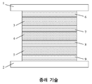
다층 구조체에 기반하는 공지된 에너지 저장 디바이스가 존재한다. 에너지 저장 디바이스는 제 1 및 제 2 전극들을 포함하며, 다층 구조체는 차단 및 유전체 층들을 포함한다. 제 1 차단 층은 제 1 전극과 유전체 층 사이에 배치되며, 제 2 차단 층은 제 2 전극과 유전체 층 사이에 배치된다. 제 1 및 제 2 차단 층들의 유전 상수들 둘 모두는 개별적으로 유전체 층의 유전 상수보다 더 크다. 도 1은, 전극들(1 및 2)을 포함하며, 다층 구조체가 차단 재료의 층들(6, 7, 8, 9)에 의해 분리되는 유전체 재료로 만들어진 층들(3, 4, 5)을 포함하는, 하나의 예시적인 설계를 도시한다. 따라서 차단 층들(6 및 9)은 전극들(1 및 2)의 근방에 배치되며, 유전체 재료의 유전 상수보다 더 높은 유전 상수에 의해 특징지어진다. 이러한 디바이스의 단점은, 전극들과 직접적으로 접촉하도록 위치된 높은 유전체 유전율의 차단 층들이 에너지 저장 디바이스의 파괴를 초래할 수 있다는 것이다. 복합 재료들에 기반하며 (PANI 입자들과 같은) 극성화된 입자들을 함유하는 높은 유전체 유전율을 갖는 재료들은 퍼콜레이션 현상을 보여줄 수 있다. 형성된 층들의 다결정질 구조체는, 결정자들 사이의 경계들 상에 다수의 얽힌 화학 결합(tangling chemical bond)들을 갖는다. 사용되는 높은 유전체 유전율을 갖는 재료가 다결정질 구조를 가질 때, 퍼콜레이션이 결정립(crystal grain)의 경계들을 따라 발생할 수 있다. 공지된 디바이스의 다른 단점은, 모든 층들의 진공 증착인 비싼 제조 절차이다.There are known energy storage devices based on multilayer structures. The energy storage device comprises first and second electrodes, wherein the multilayer structure comprises barrier and dielectric layers. A first blocking layer is disposed between the first electrode and the dielectric layer, and a second blocking layer is disposed between the second electrode and the dielectric layer. Both of the dielectric constants of the first and second barrier layers are individually greater than the dielectric constant of the dielectric layer. Figure 1 shows a multilayer
에너지 저장 디바이스로서 커패시터들은, 예를 들어 배터리와 같은 전기화학적 에너지 저장장치와 대비할 때 공지된 이점들을 갖는다. 배터리들과 비교하면, 커패시터들은 매우 높은 전력 밀도, 즉, 충전/재충전 레이트(rate)를 가지고 에너지를 저장하는 것이 가능하며, 아주 작은 열화를 갖는 긴 저장 수명을 가지는 것이 가능하고, 수십만번 또는 수억번 충전 및 방전(사이클링)될 수 있다. 그러나, 커패시터들은 일반적으로 배터리의 경우와 같이 작은 체적 또는 중량으로, 또는 낮은 에너지 저장 비용으로 에너지를 저장할 수 없으며, 이는 커패시터들을 일부 애플리케이션들, 예를 들어 전기 차량들에 대하여 비실용적으로 만든다. 따라서, 더 높은 체적 및 질량 에너지 저장 밀도 및 더 낮은 비용의 커패시터들을 제공하는 것이 에너지 저장 기술에 있어서의 진보일 것이다.Capacitors as energy storage devices have known advantages when compared to electrochemical energy storage devices such as, for example, batteries. Compared to batteries, capacitors are capable of storing energy with a very high power density, i.e. charge / refill rate, and are capable of having a long shelf life with very little degradation, Charge and discharge (cycling). However, capacitors are generally unable to store energy with small volume or weight, or low energy storage cost, as in the case of a battery, which makes the capacitors impractical for some applications, e.g., electric vehicles. Accordingly, it would be an advance in energy storage technology to provide capacitors with higher volume and mass energy storage densities and lower cost.
본 발명은 커패시터의 보존되는 에너지의 체적 및 질량 밀도의 추가적인 증가의 문제점을 해결하며, 동시에 재료들 및 제조 프로세스의 비용을 감소시킨다.The present invention solves the problem of the additional increase in the volume and mass density of the energy conserved in the capacitor, while simultaneously reducing the cost of materials and manufacturing processes.
본 발명의 실시예들은, 제 1 전극, 제 2 전극, 및 상기 제 1 및 제 2 전극들 사이에 배치된 분자 재료의 유전체 층을 포함하는 커패시터를 제공한다. 상기 전극들은 평평하고 평면적이며, 서로 평행하게 배치된다. 분자 재료는 다음의 일반식에 의해 설명된다: Embodiments of the present invention provide a capacitor comprising a first electrode, a second electrode, and a dielectric layer of molecular material disposed between the first and second electrodes. The electrodes are flat and planar and arranged parallel to one another. The molecular material is described by the following general formula:
Dp-(코어)-Hq, 일반식 (I),D p - (core) -H q , general formulas (I),
여기에서 코어는 공액(conjugated) π-시스템들을 가지며 길이방향 축에 의해 특징지어지는 극성화가능(polarizable) 전도성 비등축(anisometric) 코어이며, D 및 H는 절연 치환체(substituent)들이고, p 및 q는 그에 따른 D 및 H 치환체들의 수들이다. 절연 치환체들은 정점(apex) 위치들에서 극성화가능 비등축 코어에 부착되며, p 및 q는 값들 1, 2, 3, 4, 및 5로부터 독립적으로 선택된다.Wherein the core is a polarizable conductive anisometric core having conjugated? Systems and characterized by a longitudinal axis, D and H are insulating substituents, p and q Is the number of D and H substituents accordingly. Insulation substituents are attached to the polarizable non-excited core at apex positions, and p and q are independently selected from
커패시터를 생산하는 방법은, a) 전극들 중 하나로서 역할하는 전도성 기판을 마련하는 단계, b) 기판 상에 분자 재료를 적용(apply)하는 단계, c) 기판 상에 고체 층인 분자 재료 층을 형성하는 단계, 및 d) 고체 분자 재료 층 상에 제 2 전극을 형성하는 단계를 포함하며, 여기에서 분자 재료는 다음의 일반식에 의해 설명되고: The method of producing a capacitor comprises the steps of: a) providing a conductive substrate serving as one of the electrodes, b) applying a molecular material on the substrate, c) forming a layer of molecular material, And d) forming a second electrode on the solid molecular material layer, wherein the molecular material is described by the following general formula: < RTI ID = 0.0 >
Dp-(코어)-Hq, 일반식 (I),Dp- (core) -Hq, general formula (I),
여기에서 코어는 공액 π-시스템들을 가지며 길이방향 축에 의해 특징지어지는 전도성이고 극성화가능한 비등축 코어이며, D 및 H는 절연 치환체들이고, p 및 q는 그에 따른 D 및 H 치환체들의 수들이다. 절연 치환체들은 정점 위치들에서 극성화가능 비등축 코어에 부착되며, p 및 q는 값들 1, 2, 3, 4, 및 5로부터 독립적으로 선택된다.Wherein the core is a conductive, polarizable boiling axis core having conjugated? Systems and characterized by a longitudinal axis, D and H are the insulating substituents, and p and q are the numbers of the corresponding D and H substituents. Insulation substituents are attached to the polarizable capable boiling core at the apex positions, and p and q are independently selected from the
도 1은 에너지 저장 디바이스를 도시하는 개략적인 예시도이다.
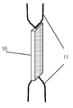
도 2는 본 발명의 일 실시예에 따른 분자 재료의 단일 분자를 도시하는 개략적인 예시도이다.
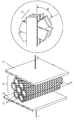
도 3은, 본 발명의 일 실시예에 따른, 분자 재료의 유전체 층 내의 육방 결정 구조를 갖는 개시된 커패시터를 도시하는 개략적인 예시도이다. 삽입도는 트위스트된(twisted) 전도성 스택(stack)의 형성을 도시하는 개략적인 예시도이다.
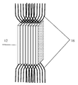
도 4는, 본 발명의 일 실시예에 따른 분자 재료의 유전체 층을 도시하는 개략적인 예시도이며, 여기에서 전도성 스택들은 0과 동일한 트위스트 각도를 가지고 형성된다.
도 5는, 본 발명의 일 실시예에 따른, 분자 재료의 유전체 층의 라멜라(lamellar) 구조를 갖는 개시된 커패시터를 도시하는 개략적인 예시도이다.Figure 1 is a schematic illustration showing an energy storage device.
2 is a schematic illustration showing a single molecule of a molecular material according to one embodiment of the present invention.
Figure 3 is a schematic illustration showing an disclosed capacitor having a hexagonal crystal structure within a dielectric layer of a molecular material, according to one embodiment of the present invention. The inset is a schematic illustration showing the formation of a twisted conductive stack.
Figure 4 is a schematic illustration showing a dielectric layer of a molecular material according to one embodiment of the present invention wherein the conductive stacks are formed with a twist angle equal to zero.
Figure 5 is a schematic illustration showing a disclosed capacitor having a lamellar structure of a dielectric layer of molecular material, in accordance with an embodiment of the present invention.
본 발명의 일반적인 설명이 이루어지며, 추가적인 이해는, 본원에서 오로지 예시적인 목적으로 그리고 첨부된 청구항들의 범위를 제한하도록 의도되지 않는 특정한 선호되는 실시예들을 참조함으로써 획득될 수 있다.A general description of the invention is given and additional understanding may be acquired by reference to certain preferred embodiments, which are not intended to be limiting for purposes of illustration and limitation of the scope of the appended claims.
본 발명은 이상에서 개시된 바와 같은 커패시터를 제공한다. 개시되는 커패시터는, 제 1 전극, 제 2 전극, 및 상기 제 1 및 제 2 전극들 사이에 배치된 분자 재료의 유전체 층을 포함한다. 상기 전극들은 평평하고 평면적이며, 서로 평행하게 배치된다. (도 2에 개략적으로 도시된) 분자 재료의 분자는 다음의 일반식에 의해 설명된다: The present invention provides a capacitor as described above. The disclosed capacitor includes a first electrode, a second electrode, and a dielectric layer of molecular material disposed between the first and second electrodes. The electrodes are flat and planar and arranged parallel to one another. The molecules of the molecular material (shown schematically in Figure 2) are illustrated by the following general formula:
Dp-(코어)-Hq, 일반식 (I),D p - (core) -H q , general formulas (I),
여기에서 코어(10)는 공액 π-시스템들을 가지며 길이방향 축에 의해 특징지어지는 극성화가능 전도성 비등축 코어이고, 절연 치환체들 D 및 H(11), p 및 q는 그에 따른 절연 치환체들 D 및 H의 수들이다. 절연 치환체들은 정점 위치들에서 극성화가능 비등축 코어에 부착되며, p 및 q는 값들 1, 2, 3, 4, 및 5로부터 독립적으로 선택된다.Wherein the core (10) is a polarizable-conductive conducting anisotropic core characterized by a longitudinal axis having conjugate? Systems, and wherein the insulating substituents D and H (11), p and q are the insulating substituents D And H. Insulation substituents are attached to the polarizable capable boiling core at the apex positions, and p and q are independently selected from the
비등축 코어는, 0.34±0.01 nm를 초과하지 않는 두께 및 동일하지 않은 치수들을 갖는 평평한 분자 시스템이다. 이는, 코어의 세로 방향을 따른 축인 길이방향 축에 의해 특징지어진다. The boiling axis core is a flat molecular system with thicknesses not equal to 0.34 + - 0.01 nm and non-identical dimensions. This is characterized by a longitudinal axis which is an axis along the longitudinal direction of the core.
개시된 커패시터의 일 실시예에 있어서, 절연 그룹들 D 중 적어도 하나 및 절연 그룹들 H 중 적어도 하나는, 알킬, 플루오르화된 알킬, 염소화된 알킬, 분지형(branched) 및 복합(complex) 알킬, 분지형 및 복합 플루오르화된 알킬, 분지형 및 복합 염소화된 알킬 그룹들, 및 이들의 임의의 조합을 포함하는 리스트로부터 독립적으로 선택된다.In one embodiment of the disclosed capacitor, at least one of the insulating groups D and at least one of the insulating groups H is selected from the group consisting of alkyl, fluorinated alkyl, chlorinated alkyl, branched and complex alkyl, Is selected independently from a list comprising terpolymers and complex fluorinated alkyls, branched and complex chlorinated alkyl groups, and any combination thereof.
개시된 커패시터의 일 실시예에 있어서, 비등축 코어는 π-π-상호작용에 기인하는 전도성 스택들을 형성하며, 절연 치환체들은 상기 스택들을 둘러싸는 절연 서브층들을 형성한다. 인접한 비등축 코어들의 길이방향 축들은 트위스트 각도 α를 형성하며, 상기 트위스트 각도는 0° ≤ α ≤ 90°의 범위 내이고, 스택들 내의 코어들 사이의 거리는 0.34±0.1nm이다.In one embodiment of the disclosed capacitor, the boiling axis core forms conductive stacks due to pi-pi-interactions, and the insulating substituents form insulating sub-layers surrounding the stacks. The longitudinal axes of adjacent boiling shafts form a twist angle alpha, the twist angle is in the range of 0 ° ≤ α ≤ 90 ° and the distance between the cores in the stacks is 0.34 ± 0.1 nm.
디바이스의 애플리케이션에 의존하여, 절연 치환체들을 가지고 형성된 절연 서브층 재료의 유전체 유전율 εins는 광범위한 영역 내에 있을 수 있으며; 대부분의 실시예들에 대하여 이는 약 2 내지 25 사이의 범위 내에 있다. 절연 서브층 재료는 4 eV보다 더 큰 밴드 갭(band gap)에 의해 특징지어진다. 절연 서브층은 약 0.01 V/nm 내지 10 V/nm 사이의 범위 내의 항복 필드 강도에 의해 특징지어진다. 비등축 코어들의 높은 분극성에 기인하여, 전도성 분자 스택들은 절연 서브층의 유전체 유전율 εins에 비하여 상대적으로 높은 유전체 유전율 εcor를 갖는다. 따라서, 전도성 극성화가능 스택들은, 절연 서브층의 유전체 유전율 εins보다 10 내지 10만 배 더 높은 유전체 유전율 εcor를 갖는다. 따라서 절연 서브층들 내의 전기장 강도 Eins 및 전도성 극성화가능 분자 스택들 내의 전기장 강도 Ecor은 다음을 충족시킨다: Depending on the application of the device, the dielectric permittivity? Ins of the insulating sub-layer material formed with the insulating substituents may be within a wide range; For most embodiments it is in the range of between about 2 and 25. The insulating sub-layer material is characterized by a band gap greater than 4 eV. The insulating sub-layer is characterized by a yield field strength in the range between about 0.01 V / nm and 10 V / nm. Due to the high boiling polarized axis of the core, a conductive molecule stack have a relatively high dielectric permittivity ε cor as compared to the dielectric permittivity ε of the insulating sublayer ins. Thus, the conductive polarized possible stacks, only the dielectric permittivity of 10 to 10 ins than ε of the insulating sub-layer has a higher dielectric permittivity ε cor times. Thus, the electric field strength E ins in the insulating sub-layers and the electric field strength E cor in the conductive polarizable molecule stacks satisfy:
Ecor = (εins/εcor)·Eins, 식 (1).E cor = (ε ins / ε cor ) · E ins , Eq. (1).
전기장 강도 Ecor은 전기장 강도 Eins보다 훨씬 더 작으며, 에너지 저장 디바이스에 가둬지는 전압은 절연 서브층들에 걸쳐 분포된다. 에너지 저장 디바이스의 동작 전압을 증가시키기 위하여, 절연 서브층들의 수를 증가시키는 것이 필요하다. The electric field strength E cor is much smaller than the electric field strength E ins , and the voltage confined in the energy storage device is distributed over the insulating sub-layers. In order to increase the operating voltage of the energy storage device, it is necessary to increase the number of insulating sub-layers.
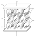
본 발명의 일 실시예에 있어서, 비등축 코어들은 트위스트된 전도성 스택들을 형성하며, 여기에서 인접한 비등축 코어들의 길이방향 축들(도 3에 대한 삽입도에서 파선들)은 트위스트 각도 α로 트위스트된다. 또 다른 실시예에 있어서, 유전체 층은 육방 결정 구조를 갖는다.In one embodiment of the present invention, the boiling shafts form twisted conductive stacks, wherein the longitudinal axes of adjacent boiling shaft cores (dashed lines in the inset in FIG. 3) are twisted with a twist angle alpha. In yet another embodiment, the dielectric layer has a hexagonal crystal structure.
도 3의 개략도에서, 커패시터는 2개의 전극들(13 및 14), 및 절연 서브층들(16)로 둘러싸인 이방성 트위스트된 스택들(12)을 포함하는 유전체 층(15)을 포함한다. 용어 "육방 구조"는 트위스트된 전도성 스택들을 포함하는 유전체 층의 분자 재료 구조를 지칭한다. 유전체 층은, 서로 평행하게 위치된 트위스트된 스택들의 조밀한 패킹(dense packing)에 의해 특징지어진다. 이러한 스택들의 이들에 대하여 직각인 평면 상으로의 돌출들이 육방 대칭성을 갖는 2-차원 구조체를 형성한다. 3, the capacitor includes a
개시된 커패시터의 일 실시예에 있어서, 비등축 코어들은 0과 동일한 트위스트 각도를 갖는 전도성 스택들을 형성한다. 하나의 스택 내의 비등축 코어들의 길이방향 축들은 서로 평행하며, 상기 전극들의 표면에 대하여 수직이다. 도 4는, 비등축 코어들을 가지고 형성된 스택(12) 및 절연 치환체들을 가지고 형성된 절연 서브층들(16)을 개략적으로 도시한다. 절연 치환체들은 전도성 스택들 사이에 그리고 또한 전도성 스택들과 전극들 사이에 절연 서브층들을 형성한다. 절연 치환체들의 추가적인 역할은 분자 재료 내의 일 함수를 증가시키는 것이다. 일 함수는, 전도성 스택의 표면으로부터 전자를 제거하기 위해 필요한 최소량의 에너지이다. In one embodiment of the disclosed capacitor, the boiling shafts form conductive stacks having the same twist angle as zero. The longitudinal axes of the boiling axis cores in one stack are parallel to one another and perpendicular to the surface of the electrodes. Figure 4 schematically shows a
또 다른 실시예에 있어서, 분자 재료는 라멜라 결정 구조를 갖는다. 라멜라 구조들 또는 마이크로구조들은, 예를 들어, 라멜라 폴리에틸렌에서와 같이, 교번하는 상이한 재료들의 미세 층들(서브층들) 및/또는 상이한 구조들 및/또는 속성들의 영역들로 구성된다. 본 발명에 있어서, 전도성 스택들의 미세 층들은 절연 치환체들의 비정질 서브층들과 교번한다. 도 5는, 본 발명의 일 실시예에 따른, 유전체 층의 라멜라 구조를 갖는 커패시터를 도시한다. 커패시터는 2개의 전극들(13 및 14), 및 극성화가능 비등축 코어들을 가지고 형성된 전도성 스택들의 미세 층들(12) 및 등방성 절연 서브층들(16)을 포함하는 유전체 층(15)을 포함한다. In yet another embodiment, the molecular material has a lamellar crystal structure. The lamellar structures or microstructures are composed of regions of different layers (sublayers) and / or different structures and / or properties of alternating different materials, such as, for example, in lamellar polyethylene. In the present invention, the microlayers of the conductive stacks alternate with the amorphous sublayers of the insulating substituents. Figure 5 illustrates a capacitor having a lamellar structure of dielectric layers, according to one embodiment of the present invention. The capacitor includes a
개시된 커패시터의 분자 재료의 극성화가능 비등축 코어들은 적어도 하나의 방향에서 병진 주기성(translation periodicity) 및 대칭성을 가질 수 있다. 병진 대칭성은, 고려되는 시스템의 속성들이 병진 벡터로 지칭되는 특정 벡터 상의 시프트에서 변화하지 않는 대칭 유형이며, 결정들은 3개의 모든 방향들에서 병진 대칭성을 갖는다. Polarizable cores of the molecular material of the disclosed capacitors may have translational periodicity and symmetry in at least one direction. The translational symmetry is a symmetric type in which the attributes of the system under consideration do not change at a shift on a particular vector, referred to as a translation vector, and the crystals have translational symmetry in all three directions.
본 발명의 일 실시예에 있어서, 극성화가능 비등축 코어는 공액 π-시스템들을 갖는 모노머들을 포함하는 전기전도성 올리고머이며, 전기전도성 올리고머는 π-π-상호작용에 기인하는 분자 스택들을 형성하고, 스택들은 평면 전극의 표면에 평행하게 위치된다. 본 발명의 일 실시예에 있어서, 전기전도성 올리고머들은 표 1에 주어지는 바와 같은 구조들(1 내지 7) 중 하나에 대응하는 다음의 구조식들을 포함하는 리스트로부터 선택된다.In one embodiment of the present invention, the polarizableizable boiling axis core is an electrically conductive oligomer comprising monomers with conjugated pi-systems, wherein the electrically conductive oligomer forms molecular stacks due to pi-pi-interactions, The stacks are positioned parallel to the surface of the planar electrode. In one embodiment of the present invention, the electrically conductive oligomers are selected from the list comprising the following structural formulas corresponding to one of structures (1 to 7) as given in Table 1:
표 1. 전기전도성 올리고머들의 예들Table 1. Examples of electrically conductive oligomers


여기에서 n은 2, 3, 4, 5, 6, 7, 8, 9, 10, 11 또는 12이다.Where n is 2, 3, 4, 5, 6, 7, 8, 9, 10, 11 or 12.
개시된 커패시터의 전극들은, 비제한적으로 Pt, Cu, Al, Ag 또는 Au를 포함하는 임의의 적절한 재료로 만들어질 수 있다. The electrodes of the disclosed capacitors can be made of any suitable material including, but not limited to Pt, Cu, Al, Ag or Au.
일부 실시예들에 있어서, 커패시터는 다양한 제조 방법들에 의해 생산될 수 있으며, 이러한 제조 방법들은 일반적으로, a) 전극들 중 하나로서 역할하는 전도성 기판을 마련하는 단계, b) 기판 상에 분자 재료를 적용(apply)하는 단계, c) 기판 상에 고체 층인 분자 재료 층을 형성하는 단계, 및 d) 고체 분자 재료 층 상에 제 2 전극을 형성하는 단계를 포함하며, 여기에서 분자 재료는 다음의 일반식에 의해 설명되고: In some embodiments, the capacitor can be produced by a variety of manufacturing methods, which generally include the steps of: a) providing a conductive substrate serving as one of the electrodes, b) C) forming a molecular material layer that is a solid layer on the substrate, and d) forming a second electrode on the solid molecular material layer, wherein the molecular material is selected from the group consisting of Described by a general formula:
Dp-(코어)-Hq, 일반식 (I),D p - (core) -H q , general formulas (I),
여기에서 코어(10)는 공액 π-시스템들을 가지며 길이방향 축에 의해 특징지어지는 극성화가능 전도성 비등축 코어이며, D 및 H는 절연 치환체들이고, p 및 q는 그에 따른 D 및 H 치환체들의 수들이다. 절연 치환체들은 정점 위치들에서 극성화가능 비등축 코어에 부착되며, p 및 q는 값들 1, 2, 3, 4, 및 5로부터 독립적으로 선택된다. Wherein the
개시된 방법의 일 실시예에 있어서, 절연 그룹들 D 중 적어도 하나 및 절연 그룹들 H 중 적어도 하나는, 알킬, 플루오르화된 알킬, 염소화된 알킬, 분지형 및 복합 알킬, 분지형 및 복합 플루오르화된 알킬, 분지형 및 복합 염소화된 알킬 그룹들, 및 이들의 임의의 조합을 포함하는 리스트로부터 독립적으로 선택된다.In one embodiment of the disclosed method, at least one of the insulating groups D and at least one of the insulating groups H is selected from the group consisting of alkyl, fluorinated alkyl, chlorinated alkyl, branched and complex alkyl, branched and complex fluorinated Alkyl, branched and complex chlorinated alkyl groups, and any combination thereof.
개시된 방법의 일 실시예에 있어서, 적용하는 단계 b)는 분자 재료의 용액을 적용하는 단계를 포함하며, 고체 층을 형성하는 단계 c)는 고체 분자 재료 층을 형성하기 위하여 건조하는 단계를 포함한다.In one embodiment of the disclosed method, applying step b) comprises applying a solution of molecular material, and step c) of forming a solid layer comprises drying to form a layer of solid molecular material .
개시된 방법의 또 다른 실시예에 있어서, 적용하는 단계 b)는 분자 재료의 용융물을 적용하는 단계를 포함하며, 고체 층을 형성하는 단계 c)는 고체 분자 재료 층을 형성하기 위하여 냉각시키는 단계를 포함한다.In another embodiment of the disclosed method, the applying step b) comprises applying a melt of molecular material, and step c) of forming a solid layer comprises cooling to form a layer of solid molecular material do.
본 발명의 실시예들이 더 용이하게 이해될 수 있도록 하기 위하여, 다음의 예에 대한 참조가 이루어지고, 이러한 예는 범위를 제한하려고 의도되지 않으며 본 발명을 예시하도록 의도된다.In order that the embodiments of the present invention may be more readily understood, reference is now made to the following examples, which are not intended to be limiting in scope and are intended to illustrate the invention.
예 1Example 1
예 1은, 도 5에 도시된 바와 같은 라멜라 구조의 고체 분자 재료로 형성된 유전체 층을 포함하는 커패시터를 설명한다.Example 1 describes a capacitor comprising a dielectric layer formed of a solid molecular material of a lamellar structure as shown in Fig.
커패시터는 2개의 전극들(13 및 14), 및 극성화가능 비등축 코어들을 가지고 형성된 전도성 비등축 스택들(12) 및 등방성 절연 서브층들(16)을 포함하는 유전체 층(15)을 포함한다. 폴리아닐린(PANI)은 극성화가능 비등축 코어로서 사용되며, 플루오르화된 알킬 치환체들이 절연 치환체들로서 사용된다. 폴리아닐린(PANI)을 가지고 형성된 전도성 비등축 스택들은 10,000과 동일한 유전체 유전율 εcor를 갖는다. 치환체들에 의해 형성된 각각의 절연 서브층들의 두께는 대략 dins=2 nm이며, 절연 서브층들의 수 nins는 500과 동일하다. 전극들(13 및 14)은 구리로 만들어진다. 절연 서브층들의 유전체 유전율은 2.2와 동일하며(즉, εins=2.2), 그것의 항복 전압은 1 V/nm와 동일하다. 커패시터의 동작 전압은, 대략 1000 V와 동일한 항복 전압 Vbd를 초과하지 않는다. The capacitor includes a
본 발명이 특정한 선호되는 실시예를 참조하여 설명되었지만, 당업자들은 다음의 청구항들의 사상 및 범위로부터 벗어나지 않고 다양한 수정들 및 향상들이 이루어질 수 있다는 것을 인식할 것이다.Although the present invention has been described with reference to certain preferred embodiments, those skilled in the art will recognize that various modifications and improvements can be made without departing from the spirit and scope of the following claims.
Claims (16)
제 1 전극,
제 2 전극, 및
상기 제 1 및 제 2 전극들 사이에 배치된 분자 재료의 유전체 층을 포함하며,
상기 전극들은 평평하고 평면적이며, 서로 평행하게 배치되고,
상기 분자 재료는 다음의 일반식에 의해 설명되며:
Dp-(코어)-Hq 일반식 (I),
여기에서 코어는 공액 π-시스템들을 가지며 길이방향 축에 의해 특징지어지는 극성화가능(polarizable) 전도성 비등축(anisometric) 코어이고,
D 및 H는 절연 치환체들이며,
p 및 q는 그에 따른 D 및 H 치환체들의 수이고,
상기 치환체들은 정점 위치들에서 상기 극성화가능 비등축 코어에 부착되며, p 및 q는 값들 1, 2, 3, 4, 및 5로부터 독립적으로 선택되는, 커패시터.
As a capacitor,
The first electrode,
A second electrode, and
A dielectric layer of molecular material disposed between the first and second electrodes,
The electrodes are flat and planar, arranged parallel to each other,
The molecular material is described by the following general formula:
D p - (core) -H q General formula (I),
Wherein the core is a polarizable conductive anisometric core having conjugated? Systems and characterized by a longitudinal axis,
D and H are insulating substituents,
p and q are the number of the corresponding D and H substituents,
Wherein the substituents are attached to the polarizable capable boiling core at apex positions, and p and q are independently selected from values 1, 2, 3, 4, and 5.
상기 절연 그룹들 D 중 적어도 하나 및 상기 절연 그룹들 H 중 적어도 하나는 각기, 알킬, 플루오르화된 알킬, 염소화된 알킬, 분지형 및 복합 알킬, 분지형 및 복합 플루오르화된 알킬, 분지형 및 복합 염소화된 알킬 그룹들, 및 이들의 임의의 조합으로 구성된 그룹으로부터 독립적으로 선택되는, 커패시터.
The method according to claim 1,
At least one of said insulation groups D and at least one of said insulation groups H is selected from the group consisting of alkyl, fluorinated alkyl, chlorinated alkyl, branched and complex alkyl, branched and complex fluorinated alkyl, Chlorinated alkyl groups, and any combination thereof.
상기 비등축 코어들은 π-π-상호작용에 기인하는 전도성 스택들을 형성하며, 상기 절연 치환체들은 상기 스택들을 둘러싸는 절연 서브층들을 형성하고, 트위스트 각도 α는 인접한 비등축 코어들의 길이방향 축들 사이에 형성되며, 상기 트위스트 각도는 0° ≤ α ≤ 90°의 범위 내이고, 상기 스택들 내의 상기 코어들 사이의 거리는 0.34±0.1nm인, 커패시터.
The method according to claim 1,
Wherein the boiling shafts form conductive stacks due to the pi-pi-interactions, the insulating substitutes form insulating sub-layers surrounding the stacks, and the twist angle alpha is between the longitudinal axes of adjacent boiling shafts Wherein the twist angle is in the range of 0 ° ≤ α ≤ 90 ° and the distance between the cores in the stacks is 0.34 ± 0.1 nm.
상기 비등축 코어들은 트위스트된 전도성 스택들을 형성하며, 상기 트위스트 각도는 0° < α ≤ 90°인, 커패시터.
The method of claim 3,
Wherein the boiling shafts form twisted conductive stacks, wherein the twist angle is 0 DEG < alpha < 90 DEG.
상기 분자 재료의 유전체 층은 육방 결정 구조를 갖는, 커패시터.
The method of claim 4,
Wherein the dielectric layer of the molecular material has a hexagonal crystal structure.
상기 비등축 코어들은 전도성 스택들을 형성하며, 상기 트위스트 각도 α는 0이고, 상기 비등축 코어들의 상기 길이방향 축들은 상기 전극들에 수직인, 커패시터.
The method of claim 3,
Wherein the boiling shafts form conductive stacks, the twist angle alpha is zero, and the longitudinal axes of the boiling shafts are perpendicular to the electrodes.
상기 분자 재료의 유전체 층은 라멜라(lamellar) 결정 구조를 갖는, 커패시터.
The method of claim 6,
Wherein the dielectric layer of the molecular material has a lamellar crystal structure.
상기 극성화가능 비등축 코어들은 적어도 하나의 방향에서 병진 주기성 및 대칭성을 갖는, 커패시터.
The method of claim 7,
Wherein the polarizable boiling axis cores have translational periodicity and symmetry in at least one direction.
상기 극성화가능 비등축 코어는 전기전도성 올리고머이며, 상기 전기전도성 올리고머들은 π-π-상호작용에 기인하는 분자 스택들을 형성하는, 커패시터.
The method according to claim 1,
Wherein the polarizable anisotropic core is an electrically conductive oligomer and the electrically conductive oligomers form molecular stacks due to a pi-pi-interaction.
상기 전기전도성 올리고머는 다음의 구조식들 1 내지 7로 구성된 그룹으로부터 선택되며, 상기 구조식들 1 내지 7은:


여기에서 n = 2, 3, 4, 5, 6, 7, 8, 9, 10, 11 또는 12인, 커패시터.
The method of claim 9,
Wherein the electroconductive oligomer is selected from the group consisting of the following structural formulas 1 to 7, wherein the structural formulas 1 to 7 are:
Wherein n = 2, 3, 4, 5, 6, 7, 8, 9, 10, 11 or 12.
상기 전극들은 Pt, Cu, Al, Ag 및/또는 Au로 만들어지는, 에너지 저장 디바이스.
The method according to claim 1,
Wherein the electrodes are made of Pt, Cu, Al, Ag and / or Au.
상기 커패시터는, 구리로 만들어진 2개의 전극들, 상기 극성화가능 비등축 코어로서 폴리아닐린(PANI), 및 상기 절연 치환체들로서 플루오르화된 알킬 치환체들을 포함하는, 커패시터.
The method according to claim 1,
Wherein the capacitor comprises two electrodes made of copper, polyaniline (PANI) as the polarizable boiling axis core, and fluorinated alkyl substituents as the insulating substituents.
a) 전극들 중 하나로서 역할하는 전도성 기판을 마련하는 단계,
b) 상기 기판 상에 분자 재료를 적용하는 단계,
c) 상기 분자 재료의 고체 층을 형성하는 단계, 및
d) 상기 고체 분자 재료 층 상에 제 2 전극을 형성하는 단계를 포함하며,
상기 분자 재료는 다음의 일반식에 의해 설명되고:
Dp-(코어)-Hq 일반식 (I),
여기에서 코어는 공액 π-시스템들을 가지며 길이방향 축에 의해 특징지어지고,
D 및 H는 절연 치환체들이며,
p 및 q는 그에 따른 D 및 H 치환체들의 수이고,
상기 치환체들은 정점 위치들에서 상기 극성화가능 비등축 코어에 부착되며, p 및 q는 값들 1, 2, 3, 4, 및 5로부터 독립적으로 선택되는, 방법.
A method of producing a capacitor,
a) providing a conductive substrate serving as one of the electrodes,
b) applying a molecular material on the substrate,
c) forming a solid layer of the molecular material, and
d) forming a second electrode on the solid molecular material layer,
The molecular material is described by the following general formula:
D p - (core) -H q General formula (I),
Wherein the core has conjugate? Systems and is characterized by a longitudinal axis,
D and H are insulating substituents,
p and q are the number of the corresponding D and H substituents,
Wherein the substituents are attached to the polarizable capable boiling core at the apex positions, and p and q are independently selected from the values 1, 2, 3, 4, and 5.
상기 절연 그룹들 D 및 H 중 적어도 하나는, 알킬, 플루오르화된 알킬, 염소화된 알킬, 분지형 및 복합 알킬, 분지형 및 복합 플루오르화된 알킬, 분지형 및 복합 염소화된 알킬 그룹들, 및 이들의 임의의 조합을 포함하는 리스트로부터 독립적으로 선택되는, 방법.
14. The method of claim 13,
At least one of said insulating groups D and H is selected from the group consisting of alkyl, fluorinated alkyl, chlorinated alkyl, branched and complex alkyl, branched and complex fluorinated alkyl, branched and complex chlorinated alkyl groups, ≪ / RTI > is selected independently from a list comprising any combination of < RTI ID = 0.0 >
상기 적용하는 단계 b)는 분자 재료의 용액을 적용하는 단계를 포함하며, 상기 고체 층을 형성하는 단계 c)는 고체 분자 재료 층을 형성하기 위하여 건조하는 단계를 포함하는, 방법.
14. The method of claim 13,
Said applying step b) comprises applying a solution of molecular material, wherein step c) of forming said solid layer comprises drying to form a solid molecular material layer.
상기 적용하는 단계 b)는 분자 재료의 용융물을 적용하는 단계를 포함하며, 상기 고체 층을 형성하는 단계 c)는 고체 분자 재료 층을 형성하기 위하여 냉각시키는 단계를 포함하는, 방법.14. The method of claim 13,
Said applying step b) comprises applying a melt of molecular material, wherein step c) of forming said solid layer comprises cooling to form a solid molecular material layer.
Applications Claiming Priority (3)
| Application Number | Priority Date | Filing Date | Title |
|---|---|---|---|
| US201461991871P | 2014-05-12 | 2014-05-12 | |
| US61/991,871 | 2014-05-12 | ||
| PCT/US2015/030356 WO2015175522A1 (en) | 2014-05-12 | 2015-05-12 | Capacitor and method of production thereof |
Publications (1)
| Publication Number | Publication Date |
|---|---|
| KR20170005821A true KR20170005821A (en) | 2017-01-16 |
Family
ID=54480548
Family Applications (1)
| Application Number | Title | Priority Date | Filing Date |
|---|---|---|---|
| KR1020167033251A KR20170005821A (en) | 2014-05-12 | 2015-05-12 | Capacitor and method of production thereof |
Country Status (14)
| Country | Link |
|---|---|
| US (1) | US9589727B2 (en) |
| EP (1) | EP3143651B1 (en) |
| JP (2) | JP2017520128A (en) |
| KR (1) | KR20170005821A (en) |
| CN (1) | CN106463618B (en) |
| AU (1) | AU2015259345B2 (en) |
| CA (1) | CA2948008A1 (en) |
| IL (1) | IL248829A0 (en) |
| MX (1) | MX2016014827A (en) |
| RU (1) | RU2016143559A (en) |
| SG (1) | SG11201609438UA (en) |
| TW (1) | TW201618139A (en) |
| WO (1) | WO2015175522A1 (en) |
| ZA (1) | ZA201608040B (en) |
Families Citing this family (28)
| Publication number | Priority date | Publication date | Assignee | Title |
|---|---|---|---|---|
| US10319523B2 (en) | 2014-05-12 | 2019-06-11 | Capacitor Sciences Incorporated | Yanli dielectric materials and capacitor thereof |
| MX2016014825A (en) | 2014-05-12 | 2017-03-10 | Capacitor Sciences Inc | Energy storage device and method of production thereof. |
| US20170301477A1 (en) * | 2016-04-04 | 2017-10-19 | Capacitor Sciences Incorporated | Electro-polarizable compound and capacitor |
| US10347423B2 (en) | 2014-05-12 | 2019-07-09 | Capacitor Sciences Incorporated | Solid multilayer structure as semiproduct for meta-capacitor |
| US10340082B2 (en) | 2015-05-12 | 2019-07-02 | Capacitor Sciences Incorporated | Capacitor and method of production thereof |
| JP6668341B2 (en) | 2014-11-04 | 2020-03-18 | キャパシタ サイエンシス インコーポレイテッド | Energy storage device and method of manufacturing the same |
| CA2977776A1 (en) | 2015-02-26 | 2016-09-01 | Capacitor Sciences Incorporated | Self-healing capacitor and methods of production thereof |
| US9932358B2 (en) | 2015-05-21 | 2018-04-03 | Capacitor Science Incorporated | Energy storage molecular material, crystal dielectric layer and capacitor |
| US9941051B2 (en) | 2015-06-26 | 2018-04-10 | Capactor Sciences Incorporated | Coiled capacitor |
| US10026553B2 (en) | 2015-10-21 | 2018-07-17 | Capacitor Sciences Incorporated | Organic compound, crystal dielectric layer and capacitor |
| DE102015224739A1 (en) * | 2015-12-09 | 2017-06-14 | Robert Bosch Gmbh | Method and device for triggering pedestrian protection devices and / or pedestrian warning devices |
| US10636575B2 (en) | 2016-02-12 | 2020-04-28 | Capacitor Sciences Incorporated | Furuta and para-Furuta polymer formulations and capacitors |
| US20170236642A1 (en) * | 2016-02-12 | 2017-08-17 | Capacitor Sciences Incorporated | para-FURUTA POLYMER AND CAPACITOR |
| US20170233528A1 (en) * | 2016-02-12 | 2017-08-17 | Capacitor Sciences Incorporated | Sharp polymer and capacitor |
| US10305295B2 (en) | 2016-02-12 | 2019-05-28 | Capacitor Sciences Incorporated | Energy storage cell, capacitive energy storage module, and capacitive energy storage system |
| US20170236641A1 (en) * | 2016-02-12 | 2017-08-17 | Capacitor Sciences Incorporated | Furuta co-polymer and capacitor |
| US11092142B2 (en) * | 2017-11-20 | 2021-08-17 | Capacitor Sciences Incorporated | Plasma electric propulsion device |
| US20170283618A1 (en) * | 2016-04-04 | 2017-10-05 | Capacitor Sciences Incorporated | Non-linear dielectric materials and capacitor |
| US10153087B2 (en) | 2016-04-04 | 2018-12-11 | Capacitor Sciences Incorporated | Electro-polarizable compound and capacitor |
| US9978517B2 (en) | 2016-04-04 | 2018-05-22 | Capacitor Sciences Incorporated | Electro-polarizable compound and capacitor |
| WO2018021328A1 (en) * | 2016-07-26 | 2018-02-01 | 日産化学工業株式会社 | Polymer composition |
| US10395841B2 (en) | 2016-12-02 | 2019-08-27 | Capacitor Sciences Incorporated | Multilayered electrode and film energy storage device |
| US10388461B2 (en) | 2017-08-02 | 2019-08-20 | Perriquest Defense Research Enterprises, Llc | Capacitor arrangements |
| US10163575B1 (en) * | 2017-11-07 | 2018-12-25 | Capacitor Sciences Incorporated | Non-linear capacitor and energy storage device comprising thereof |
| JP2021503488A (en) * | 2017-11-20 | 2021-02-12 | キャパシター サイエンシズ インコーポレイテッドCapacitor Sciences Incorporated | Hein electron-polarizing compounds and their capacitors |
| US10403435B2 (en) | 2017-12-15 | 2019-09-03 | Capacitor Sciences Incorporated | Edder compound and capacitor thereof |
| US11476261B2 (en) * | 2019-02-27 | 2022-10-18 | Kepler Computing Inc. | High-density low voltage non-volatile memory with unidirectional plate-line and bit-line and pillar capacitor |
| JP7444561B2 (en) | 2019-08-08 | 2024-03-06 | 株式会社東芝 | Aluminum electrolytic capacitor, electrical equipment, and method for manufacturing aluminum electrolytic capacitor |
Family Cites Families (19)
| Publication number | Priority date | Publication date | Assignee | Title |
|---|---|---|---|---|
| US6501093B1 (en) | 1994-04-04 | 2002-12-31 | Alvin M. Marks | Quantum energy storage or retrieval device |
| US7033406B2 (en) | 2001-04-12 | 2006-04-25 | Eestor, Inc. | Electrical-energy-storage unit (EESU) utilizing ceramic and integrated-circuit technologies for replacement of electrochemical batteries |
| EP1433211B1 (en) * | 2001-09-27 | 2006-06-21 | 3M Innovative Properties Company | Substituted pentacene semiconductors |
| DE10248722A1 (en) * | 2002-10-18 | 2004-05-06 | Infineon Technologies Ag | Integrated circuit arrangement with capacitor and manufacturing process |
| US7122063B2 (en) * | 2003-02-07 | 2006-10-17 | Showa Denko K.K. | Capacitor and production method of the capacitor |
| US7466536B1 (en) | 2004-08-13 | 2008-12-16 | Eestor, Inc. | Utilization of poly(ethylene terephthalate) plastic and composition-modified barium titanate powders in a matrix that allows polarization and the use of integrated-circuit technologies for the production of lightweight ultrahigh electrical energy storage units (EESU) |
| JP3841814B1 (en) * | 2005-04-28 | 2006-11-08 | 三井金属鉱業株式会社 | Capacitor layer forming material and method for manufacturing the capacitor layer forming material |
| WO2007078916A2 (en) | 2005-12-28 | 2007-07-12 | The Penn State Research Foundation | High electric energy density polymer capacitors with fast discharge speed and high efficiency based on unique poly(vinylidene fluoride) copolymers and terpolymers as dielectric materials |
| US20080002329A1 (en) * | 2006-07-02 | 2008-01-03 | Pohm Arthur V | High Dielectric, Non-Linear Capacitor |
| GB0616358D0 (en) * | 2006-08-16 | 2006-09-27 | Crysoptix Ltd | Anisotropic polymer film and method of production thereof |
| GB0622150D0 (en) * | 2006-11-06 | 2006-12-20 | Kontrakt Technology Ltd | Anisotropic semiconductor film and method of production thereof |
| WO2010083055A1 (en) | 2009-01-16 | 2010-07-22 | The Board Of Trustees Of The Leland Stanford Junior University | Quantum dot ultracapacitor and electron battery |
| US8524398B2 (en) | 2009-04-01 | 2013-09-03 | The Board Of Trustees Of The Leland Stanford Junior University | All-electron battery having area-enhanced electrodes |
| KR20110122051A (en) | 2010-05-03 | 2011-11-09 | 제일모직주식회사 | Compound for organic photoelectric device and organic photoelectric device including the same |
| US20120008251A1 (en) * | 2010-07-12 | 2012-01-12 | Wei-Ching Yu | Film capacitors comprising melt-stretched films as dielectrics |
| KR101517532B1 (en) * | 2011-07-05 | 2015-05-04 | 가부시키가이샤 무라타 세이사쿠쇼 | Dielectric thin film, dielectric thin film element, and thin film capacitor |
| CN104053689B (en) * | 2011-12-09 | 2017-01-18 | 南洋理工大学 | Graft copolymers of a poly(vinylidene fluoride)-based polymer and at least one type of electrically conductive polymer, and methods for forming the graft copolymers |
| US9087645B2 (en) | 2012-01-30 | 2015-07-21 | QuantrumScape Corporation | Solid state energy storage devices |
| US20130334657A1 (en) * | 2012-06-15 | 2013-12-19 | Taiwan Semiconductor Manufacturing Co., Ltd. | Planar interdigitated capacitor structures and methods of forming the same |
-
2015
- 2015-05-12 CA CA2948008A patent/CA2948008A1/en not_active Abandoned
- 2015-05-12 CN CN201580025110.6A patent/CN106463618B/en active Active
- 2015-05-12 RU RU2016143559A patent/RU2016143559A/en not_active Application Discontinuation
- 2015-05-12 SG SG11201609438UA patent/SG11201609438UA/en unknown
- 2015-05-12 TW TW104115076A patent/TW201618139A/en unknown
- 2015-05-12 MX MX2016014827A patent/MX2016014827A/en unknown
- 2015-05-12 US US14/710,491 patent/US9589727B2/en active Active
- 2015-05-12 KR KR1020167033251A patent/KR20170005821A/en not_active Application Discontinuation
- 2015-05-12 AU AU2015259345A patent/AU2015259345B2/en not_active Ceased
- 2015-05-12 EP EP15792405.1A patent/EP3143651B1/en active Active
- 2015-05-12 WO PCT/US2015/030356 patent/WO2015175522A1/en active Application Filing
- 2015-05-12 JP JP2017512654A patent/JP2017520128A/en active Pending
-
2016
- 2016-11-08 IL IL248829A patent/IL248829A0/en unknown
- 2016-11-21 ZA ZA2016/08040A patent/ZA201608040B/en unknown
-
2020
- 2020-04-24 JP JP2020077405A patent/JP2020120130A/en active Pending
Also Published As
| Publication number | Publication date |
|---|---|
| CN106463618A (en) | 2017-02-22 |
| US20160020027A1 (en) | 2016-01-21 |
| CN106463618B (en) | 2019-06-14 |
| CA2948008A1 (en) | 2015-11-19 |
| EP3143651A1 (en) | 2017-03-22 |
| JP2017520128A (en) | 2017-07-20 |
| JP2020120130A (en) | 2020-08-06 |
| SG11201609438UA (en) | 2016-12-29 |
| EP3143651B1 (en) | 2020-09-16 |
| AU2015259345B2 (en) | 2018-03-01 |
| US9589727B2 (en) | 2017-03-07 |
| ZA201608040B (en) | 2018-11-28 |
| WO2015175522A1 (en) | 2015-11-19 |
| AU2015259345A1 (en) | 2016-11-24 |
| MX2016014827A (en) | 2017-03-10 |
| IL248829A0 (en) | 2017-01-31 |
| EP3143651A4 (en) | 2017-12-13 |
| TW201618139A (en) | 2016-05-16 |
| RU2016143559A (en) | 2018-06-19 |
Similar Documents
| Publication | Publication Date | Title |
|---|---|---|
| KR20170005821A (en) | Capacitor and method of production thereof | |
| KR102331588B1 (en) | Energy storage device and method of production thereof | |
| KR102461254B1 (en) | Energy storage devices and methods of production thereof | |
| US10685782B2 (en) | Capacitor and method of production thereof | |
| US20170236642A1 (en) | para-FURUTA POLYMER AND CAPACITOR |
Legal Events
| Date | Code | Title | Description |
|---|---|---|---|
| E902 | Notification of reason for refusal | ||
| E90F | Notification of reason for final refusal | ||
| E601 | Decision to refuse application |