KR20160105442A - Optical film including collimating reflective polarizer - Google Patents
Optical film including collimating reflective polarizer Download PDFInfo
- Publication number
- KR20160105442A KR20160105442A KR1020167020406A KR20167020406A KR20160105442A KR 20160105442 A KR20160105442 A KR 20160105442A KR 1020167020406 A KR1020167020406 A KR 1020167020406A KR 20167020406 A KR20167020406 A KR 20167020406A KR 20160105442 A KR20160105442 A KR 20160105442A
- Authority
- KR
- South Korea
- Prior art keywords
- optical film
- optical
- reflective polarizer
- light
- array
- Prior art date
Links
Images


Classifications
-
- G—PHYSICS
- G02—OPTICS
- G02B—OPTICAL ELEMENTS, SYSTEMS OR APPARATUS
- G02B5/00—Optical elements other than lenses
- G02B5/30—Polarising elements
- G02B5/3025—Polarisers, i.e. arrangements capable of producing a definite output polarisation state from an unpolarised input state
- G02B5/3033—Polarisers, i.e. arrangements capable of producing a definite output polarisation state from an unpolarised input state in the form of a thin sheet or foil, e.g. Polaroid
- G02B5/3041—Polarisers, i.e. arrangements capable of producing a definite output polarisation state from an unpolarised input state in the form of a thin sheet or foil, e.g. Polaroid comprising multiple thin layers, e.g. multilayer stacks
- G02B5/305—Polarisers, i.e. arrangements capable of producing a definite output polarisation state from an unpolarised input state in the form of a thin sheet or foil, e.g. Polaroid comprising multiple thin layers, e.g. multilayer stacks including organic materials, e.g. polymeric layers
-
- G—PHYSICS
- G02—OPTICS
- G02B—OPTICAL ELEMENTS, SYSTEMS OR APPARATUS
- G02B5/00—Optical elements other than lenses
- G02B5/30—Polarising elements
- G02B5/3025—Polarisers, i.e. arrangements capable of producing a definite output polarisation state from an unpolarised input state
- G02B5/3033—Polarisers, i.e. arrangements capable of producing a definite output polarisation state from an unpolarised input state in the form of a thin sheet or foil, e.g. Polaroid
-
- G—PHYSICS
- G02—OPTICS
- G02B—OPTICAL ELEMENTS, SYSTEMS OR APPARATUS
- G02B27/00—Optical systems or apparatus not provided for by any of the groups G02B1/00 - G02B26/00, G02B30/00
- G02B27/28—Optical systems or apparatus not provided for by any of the groups G02B1/00 - G02B26/00, G02B30/00 for polarising
- G02B27/283—Optical systems or apparatus not provided for by any of the groups G02B1/00 - G02B26/00, G02B30/00 for polarising used for beam splitting or combining
-
- G—PHYSICS
- G02—OPTICS
- G02B—OPTICAL ELEMENTS, SYSTEMS OR APPARATUS
- G02B27/00—Optical systems or apparatus not provided for by any of the groups G02B1/00 - G02B26/00, G02B30/00
- G02B27/30—Collimators
-
- G—PHYSICS
- G02—OPTICS
- G02B—OPTICAL ELEMENTS, SYSTEMS OR APPARATUS
- G02B3/00—Simple or compound lenses
- G02B3/0006—Arrays
-
- G—PHYSICS
- G02—OPTICS
- G02B—OPTICAL ELEMENTS, SYSTEMS OR APPARATUS
- G02B6/00—Light guides; Structural details of arrangements comprising light guides and other optical elements, e.g. couplings
- G02B6/0001—Light guides; Structural details of arrangements comprising light guides and other optical elements, e.g. couplings specially adapted for lighting devices or systems
- G02B6/0011—Light guides; Structural details of arrangements comprising light guides and other optical elements, e.g. couplings specially adapted for lighting devices or systems the light guides being planar or of plate-like form
- G02B6/0013—Means for improving the coupling-in of light from the light source into the light guide
- G02B6/0023—Means for improving the coupling-in of light from the light source into the light guide provided by one optical element, or plurality thereof, placed between the light guide and the light source, or around the light source
- G02B6/003—Lens or lenticular sheet or layer
-
- G—PHYSICS
- G02—OPTICS
- G02B—OPTICAL ELEMENTS, SYSTEMS OR APPARATUS
- G02B6/00—Light guides; Structural details of arrangements comprising light guides and other optical elements, e.g. couplings
- G02B6/0001—Light guides; Structural details of arrangements comprising light guides and other optical elements, e.g. couplings specially adapted for lighting devices or systems
- G02B6/0011—Light guides; Structural details of arrangements comprising light guides and other optical elements, e.g. couplings specially adapted for lighting devices or systems the light guides being planar or of plate-like form
- G02B6/0013—Means for improving the coupling-in of light from the light source into the light guide
- G02B6/0023—Means for improving the coupling-in of light from the light source into the light guide provided by one optical element, or plurality thereof, placed between the light guide and the light source, or around the light source
- G02B6/0031—Reflecting element, sheet or layer
-
- G—PHYSICS
- G02—OPTICS
- G02B—OPTICAL ELEMENTS, SYSTEMS OR APPARATUS
- G02B6/00—Light guides; Structural details of arrangements comprising light guides and other optical elements, e.g. couplings
- G02B6/0001—Light guides; Structural details of arrangements comprising light guides and other optical elements, e.g. couplings specially adapted for lighting devices or systems
- G02B6/0011—Light guides; Structural details of arrangements comprising light guides and other optical elements, e.g. couplings specially adapted for lighting devices or systems the light guides being planar or of plate-like form
- G02B6/0033—Means for improving the coupling-out of light from the light guide
- G02B6/005—Means for improving the coupling-out of light from the light guide provided by one optical element, or plurality thereof, placed on the light output side of the light guide
- G02B6/0053—Prismatic sheet or layer; Brightness enhancement element, sheet or layer
-
- G—PHYSICS
- G02—OPTICS
- G02B—OPTICAL ELEMENTS, SYSTEMS OR APPARATUS
- G02B6/00—Light guides; Structural details of arrangements comprising light guides and other optical elements, e.g. couplings
- G02B6/0001—Light guides; Structural details of arrangements comprising light guides and other optical elements, e.g. couplings specially adapted for lighting devices or systems
- G02B6/0011—Light guides; Structural details of arrangements comprising light guides and other optical elements, e.g. couplings specially adapted for lighting devices or systems the light guides being planar or of plate-like form
- G02B6/0033—Means for improving the coupling-out of light from the light guide
- G02B6/005—Means for improving the coupling-out of light from the light guide provided by one optical element, or plurality thereof, placed on the light output side of the light guide
- G02B6/0055—Reflecting element, sheet or layer
-
- G—PHYSICS
- G02—OPTICS
- G02B—OPTICAL ELEMENTS, SYSTEMS OR APPARATUS
- G02B6/00—Light guides; Structural details of arrangements comprising light guides and other optical elements, e.g. couplings
- G02B6/0001—Light guides; Structural details of arrangements comprising light guides and other optical elements, e.g. couplings specially adapted for lighting devices or systems
- G02B6/0011—Light guides; Structural details of arrangements comprising light guides and other optical elements, e.g. couplings specially adapted for lighting devices or systems the light guides being planar or of plate-like form
- G02B6/0033—Means for improving the coupling-out of light from the light guide
- G02B6/0056—Means for improving the coupling-out of light from the light guide for producing polarisation effects, e.g. by a surface with polarizing properties or by an additional polarizing elements
-
- G—PHYSICS
- G02—OPTICS
- G02F—OPTICAL DEVICES OR ARRANGEMENTS FOR THE CONTROL OF LIGHT BY MODIFICATION OF THE OPTICAL PROPERTIES OF THE MEDIA OF THE ELEMENTS INVOLVED THEREIN; NON-LINEAR OPTICS; FREQUENCY-CHANGING OF LIGHT; OPTICAL LOGIC ELEMENTS; OPTICAL ANALOGUE/DIGITAL CONVERTERS
- G02F1/00—Devices or arrangements for the control of the intensity, colour, phase, polarisation or direction of light arriving from an independent light source, e.g. switching, gating or modulating; Non-linear optics
- G02F1/01—Devices or arrangements for the control of the intensity, colour, phase, polarisation or direction of light arriving from an independent light source, e.g. switching, gating or modulating; Non-linear optics for the control of the intensity, phase, polarisation or colour
- G02F1/13—Devices or arrangements for the control of the intensity, colour, phase, polarisation or direction of light arriving from an independent light source, e.g. switching, gating or modulating; Non-linear optics for the control of the intensity, phase, polarisation or colour based on liquid crystals, e.g. single liquid crystal display cells
- G02F1/133—Constructional arrangements; Operation of liquid crystal cells; Circuit arrangements
- G02F1/1333—Constructional arrangements; Manufacturing methods
- G02F1/1335—Structural association of cells with optical devices, e.g. polarisers or reflectors
- G02F1/1336—Illuminating devices
- G02F1/133602—Direct backlight
- G02F1/133606—Direct backlight including a specially adapted diffusing, scattering or light controlling members
- G02F1/133607—Direct backlight including a specially adapted diffusing, scattering or light controlling members the light controlling member including light directing or refracting elements, e.g. prisms or lenses
-
- G02F2001/133607—
Landscapes
- Physics & Mathematics (AREA)
- General Physics & Mathematics (AREA)
- Optics & Photonics (AREA)
- Nonlinear Science (AREA)
- Mathematical Physics (AREA)
- Crystallography & Structural Chemistry (AREA)
- Chemical & Material Sciences (AREA)
- Planar Illumination Modules (AREA)
- Polarising Elements (AREA)
- Optical Elements Other Than Lenses (AREA)
- Liquid Crystal (AREA)
- Laminated Bodies (AREA)
- Securing Globes, Refractors, Reflectors Or The Like (AREA)
Abstract
광학 필름이 개시된다. 보다 구체적으로, 시준 반사 편광기를 포함하는 광학 필름이 개시된다. 광학 필름은 백라이트, 및 특히 백라이트 재순환 공동에서 유용하다. 에지형 백라이트 및 직하형 백라이트 둘 모두에 적합한 구성이 개시된다.An optical film is disclosed. More specifically, an optical film comprising a collimated reflective polarizer is disclosed. Optical films are useful in backlights, and in particular backlight recirculating cavities. A configuration suitable for both an edge type backlight and a direct type backlight is disclosed.
Description
반사 편광기는 일 편광 상태를 갖는 광을 실질적으로 투과시키면서 직교 편광 상태를 갖는 광을 실질적으로 반사시키고, 디스플레이 디바이스용 백라이트에 사용된다. 어떤 경우에, 반사 편광기는 다른 반사 표면과 결합되어 광 재순환 공동(light recycling cavity)을 생성한다. 복수의 광 지향 요소들을 갖는 미세복제된 필름이 광의 각도 분포를 변경하기 위해 사용될 수 있다.The reflective polarizer substantially reflects light having an orthogonal polarization state while substantially transmitting light having a single polarization state, and is used for a backlight for a display device. In some cases, the reflective polarizer is combined with another reflective surface to create a light recycling cavity. A microreplicated film having a plurality of light directing elements can be used to alter the angular distribution of light.
일 태양에서, 본 발명은 광학 필름에 관한 것이다. 광학 필름은 시준 반사 편광기, 및 시준 반사 편광기의 주 표면 상에 배치되는 오목 마이크로렌즈들의 어레이를 포함한다. 일부 실시 형태에서, 시준 반사 편광기는 p-편광된 광에 대해 수직 입사에서 통과 축(pass axis)을 따른 투과율이 Tpassnormal이고 p-편광된 광에 대해 60도 입사에서 통과 축을 따른 투과율이 Tpass60이고, Tpass60 대 Tpassnormal의 비가 0.75 미만이다. 일부 실시 형태에서, Tpass60 대 Tpassnormal의 비는 0.60 또는 0.50 미만이다. 일부 실시 형태에서, 오목 마이크로렌즈들의 어레이는 임의로(randomly) 배열된다. 일부 실시 형태에서, 오목 마이크로렌즈들의 어레이는 규칙적으로 배열된다. 일부 실시 형태에서, 오목 마이크로렌즈들의 어레이에서의 각각의 마이크로렌즈는 종횡비가 약 0.5이다. 일부 실시 형태에서, 오목 마이크로렌즈들의 어레이에서의 각각의 마이크로렌즈는 종횡비가 약 0.3이다. 일부 실시 형태에서, 오목 마이크로렌즈들의 어레이에서의 각각의 마이크로렌즈는 종횡비가 약 0.5 미만이다. 일부 실시 형태에서, 광학 필름은 오목 마이크로렌즈들의 어레이 상에 배치되지 않는 시준 반사 편광기의 표면 상에 배치되는 미세특징부들을 추가로 포함한다. 미세특징부들은 비드(bead)들을 포함할 수 있다. 일부 실시 형태에서, 비드들의 평균 직경은 약 8 μm이다. 일부 실시 형태에서, 미세특징부들은 볼록 렌즈들 또는 프리즘들을 포함한다. 일부 실시 형태에서, 광학 필름은 두께가 420 μm 미만이다. 일부 실시 형태에서, 에지형(edge-lit) 백라이트 조립체가 광학 필름 및 도광체를 포함하고, 여기서 도광체는 오목 마이크로렌즈들의 어레이에 근접하여 배치된다. 일부 실시 형태에서, 직하형(direct-lit) 백라이트 조립체가 광학 필름 및 하나 이상의 광원들을 포함하고, 여기서 하나 이상의 광원들은 오목 마이크로렌즈들의 어레이에 근접하여 배치된다.In one aspect, the invention relates to an optical film. The optical film comprises a collimated reflective polarizer, and an array of concave microlenses disposed on the major surface of the collimated reflective polarizer. In some embodiments, the collimated reflective polarizer has a transmittance Tpassnormal along a pass axis at normal incidence to p-polarized light and a transmittance Tpass60 along the pass axis at 60 degrees incident on p-polarized light, The ratio of Tpass 60 to Tpassnormal is less than 0.75. In some embodiments, the ratio of Tpass 60 to Tpassnormal is less than 0.60 or 0.50. In some embodiments, the array of concave microlenses is randomly arranged. In some embodiments, the array of concave microlenses is arranged regularly. In some embodiments, each microlens in the array of concave microlenses has an aspect ratio of about 0.5. In some embodiments, each microlens in the array of concave microlenses has an aspect ratio of about 0.3. In some embodiments, each microlens in the array of concave microlenses has an aspect ratio of less than about 0.5. In some embodiments, the optical film further comprises microscopic features disposed on a surface of a collimated reflective polarizer that is not disposed on an array of concave microlenses. The fine features may include beads. In some embodiments, the average diameter of the beads is about 8 占 퐉. In some embodiments, the fine features include convex lenses or prisms. In some embodiments, the optical film has a thickness of less than 420 [mu] m. In some embodiments, an edge-lit backlight assembly includes an optical film and a light guide, wherein the light guide is disposed close to the array of concave microlenses. In some embodiments, a direct-lit backlight assembly includes an optical film and one or more light sources, wherein one or more light sources are disposed close to the array of concave microlenses.
다른 태양에서, 본 발명은 제1 및 제2 주 표면을 갖는 광학 기재, 광학 기재의 제1 주 표면 상에 배치되는 시준 반사 편광기, 및 광학 기재의 제2 주 표면 상에 배치되는 오목 마이크로렌즈들의 어레이를 포함하는 광학 필름에 관한 것이다. 일부 실시 형태에서, 광학 필름은 광학 기재와 시준 반사 편광기 사이에 접착제를 추가로 포함한다. 일부 실시 형태에서, 시준 반사 편광기는 p-편광된 광에 대해 수직 입사에서 통과 축을 따른 투과율이 Tpassnormal이고 p-편광된 광에 대해 60도 입사에서 통과 축을 따른 투과율이 Tpass60이고, Tpass60 대 Tpassnormal의 비가 0.75 미만이다. 일부 실시 형태에서, Tpass60 대 Tpassnormal의 비는 0.60 또는 0.50 미만이다. 일부 실시 형태에서, 오목 마이크로렌즈들의 어레이는 임의로 배열된다. 일부 실시 형태에서, 오목 마이크로렌즈들의 어레이는 규칙적으로 배열된다. 일부 실시 형태에서, 오목 마이크로렌즈들의 어레이에서의 각각의 마이크로렌즈는 종횡비가 약 0.5이다. 일부 실시 형태에서, 오목 마이크로렌즈들의 어레이에서의 각각의 마이크로렌즈는 종횡비가 약 0.3이다. 일부 실시 형태에서, 오목 마이크로렌즈들의 어레이에서의 각각의 마이크로렌즈는 종횡비가 약 0.5 미만이다. 일부 실시 형태에서, 광학 필름은 광학 기재 상에 배치되지 않는 시준 반사 편광기의 표면 상에 배치되는 미세특징부들을 추가로 포함한다. 미세특징부들은 비드들을 포함할 수 있다. 일부 실시 형태에서, 비드들의 평균 직경은 약 8 μm이다. 일부 실시 형태에서, 미세특징부들은 볼록 렌즈들 또는 프리즘들을 포함한다. 일부 실시 형태에서, 광학 필름은 두께가 420 μm 미만이다. 일부 실시 형태에서, 에지형 백라이트 조립체가 광학 필름 및 도광체를 포함하고, 여기서 도광체는 오목 마이크로렌즈들의 어레이에 근접하여 배치된다. 일부 실시 형태에서, 직하형 백라이트 조립체가 광학 필름 및 하나 이상의 광원들을 포함하고, 여기서 하나 이상의 광원들은 오목 마이크로렌즈들의 어레이에 근접하여 배치된다.In another aspect, the present invention provides an optical device comprising an optical substrate having first and second major surfaces, a collimated reflective polarizer disposed on a first major surface of the optical substrate, and concave microlenses disposed on a second major surface of the optical substrate To an optical film comprising an array. In some embodiments, the optical film further comprises an adhesive between the optical substrate and the collimated reflective polarizer. In some embodiments, the collimated reflective polarizer has a transmittance Tpassnormal along the pass axis at normal incidence for p-polarized light and a transmittance Tpass60 along the pass axis at 60 degrees incident for p-polarized light, and a ratio of Tpass60 to Tpassnormal Lt; 0.75. In some embodiments, the ratio of Tpass 60 to Tpassnormal is less than 0.60 or 0.50. In some embodiments, the array of concave microlenses is arbitrarily arranged. In some embodiments, the array of concave microlenses is arranged regularly. In some embodiments, each microlens in the array of concave microlenses has an aspect ratio of about 0.5. In some embodiments, each microlens in the array of concave microlenses has an aspect ratio of about 0.3. In some embodiments, each microlens in the array of concave microlenses has an aspect ratio of less than about 0.5. In some embodiments, the optical film further comprises microscopic features disposed on a surface of a collimated reflective polarizer that is not disposed on the optical substrate. The fine features may include beads. In some embodiments, the average diameter of the beads is about 8 占 퐉. In some embodiments, the fine features include convex lenses or prisms. In some embodiments, the optical film has a thickness of less than 420 [mu] m. In some embodiments, the edge-type backlight assembly includes an optical film and a light guide, wherein the light guide is disposed close to the array of concave microlenses. In some embodiments, the direct underlying backlight assembly includes an optical film and one or more light sources, wherein the one or more light sources are disposed close to the array of concave microlenses.
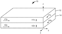
도 1은 다층 광학 필름의 개략적인 상부 사시도이다.
도 2는 시준 반사 편광기를 포함하는 광학 필름의 측단면도이다.
도 3은 시준 반사 편광기를 포함하는 다른 광학 필름의 측단면도이다.
도 4는 시준 반사 편광기를 포함하는 다른 광학 필름의 측단면도이다.
도 5는 도 2의 광학 필름을 포함하는 에지형 백라이트의 일부분의 측단면도이다.
도 6은 도 2의 광학 필름을 포함하는 직하형 백라이트의 일부분의 측단면도이다.
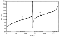
도 7은 비교예 C-2에서의 시준 반사 편광기의 층 두께 프로파일을 나타내는 그래프이다.1 is a schematic top perspective view of a multilayer optical film.
2 is a side cross-sectional view of an optical film comprising a collimated reflective polarizer.
3 is a side cross-sectional view of another optical film comprising a collimated reflective polarizer.
4 is a side cross-sectional view of another optical film comprising a collimated reflective polarizer.
5 is a side cross-sectional view of a portion of an edge-type backlight including the optical film of Fig.
Fig. 6 is a side cross-sectional view of a portion of a direct-type backlight including the optical film of Fig. 2;
7 is a graph showing the layer thickness profile of the collimated reflective polarizer in Comparative Example C-2.
도 1은 다층 광학 필름의 개략적인 상부 사시도이다. 다층 광학 필름(10)은 제1 층들(12) 및 제2 층들(14)을 포함한다.1 is a schematic top perspective view of a multilayer optical film. The multilayer
다층 광학 필름, 즉, 적어도 부분적으로는, 굴절률이 상이한 미세층(microlayer)들의 배열에 의해 바람직한 투과율 및/또는 반사율 특성을 제공하는 필름이 공지되어 있다. 진공 챔버에서 기재 상의 광학적으로 얇은 층들("미세층들")에 일련의 무기 재료들을 침착시킴으로써 그러한 다층 광학 필름을 제조하는 것이 공지되어 있다. 무기 다층 광학 필름은, 예를 들어, 문헌[H. A. Macleod, Thin-Film Optical Filters, 2nd Ed., Macmillan Publishing Co. (1986)] 및 문헌[A. Thelan, Design of Optical Interference Filters, McGraw-Hill, Inc. (1989)]의 교재에 기재되어 있다.Films are known which provide the desired transmittance and / or reflectance properties by multilayer optical films, i.e., at least in part, by arrangement of microlayers with different refractive indices. It is known to produce such multilayer optical films by depositing a series of inorganic materials in optically thin layers ("microns") on a substrate in a vacuum chamber. Inorganic multilayer optical films are described, for example, in HA Macleod, Thin-Film Optical Filters, 2nd Ed . , Macmillan Publishing Co. (1986) and A. & Thelan, Design of Optical Interference Filters , McGraw-Hill, Inc. (1989)].
다층 광학 필름은 또한 교호하는 중합체 층들의 공압출에 의해 입증되었다. 예를 들어, 미국 특허 제3,610,729호(로저스(Rogers)), 제4,446,305호(로저스 등), 제4,540,623호(임(Im) 등), 제5,448,404호(슈렝크(Schrenk) 등), 및 제5,882,774호(존자(Jonza) 등)를 참조하라. 이들 중합체 다층 광학 필름에서, 개별 층들의 제조에는 중합체 재료들이 주로 또는 배타적으로 사용된다. 그러한 필름은 대량 제조 공정에 적합하고 대형 시트 및 롤 제품으로 제조될 수 있다.Multilayer optical films have also been demonstrated by coextrusion of alternating polymer layers. For example, U.S. Patent No. 3,610,729 (Rogers), 4,446,305 (Rogers et al.), 4,540,623 (Im), 5,448,404 (Schrenk et al.), And 5,882,774 See Jonza et al. In these polymeric multilayer optical films, polymeric materials are primarily or exclusively used for the production of discrete layers. Such films are suitable for mass production processes and can be made into large sheet and roll products.
다층 광학 필름은 상이한 굴절률 특성을 갖는 개별 미세층들을 포함하여, 인접한 미세층들 사이의 계면에서 일부 광이 반사되게 한다. 다층 광학 필름에 원하는 반사율 또는 투과율 특성을 제공하기 위하여, 미세층은 복수의 계면에서 반사된 광이 보강 또는 상쇄 간섭을 겪도록 충분히 얇다. 자외선, 가시광선 또는 근적외선 파장에서 광을 반사시키도록 설계된 다층 광학 필름들의 경우, 각각의 미세층은 일반적으로 약 1 μm 미만의 광학 두께(물리적 두께에 굴절률을 곱함)를 갖는다. 다층 광학 필름의 외부 표면들에 있는 스킨 층들, 또는 미세층들의 일관된 그룹들(본 명세서에서 "패킷들"이라고 지칭됨)을 분리시키는 다층 광학 필름들 내에 배치된 보호 경계 층(PBL)들과 같은 더 두꺼운 층들이 포함될 수 있다.The multilayer optical film includes discrete microlayers having different refractive index properties to allow some light to be reflected at the interface between adjacent microlayers. In order to provide the desired reflectivity or transmittance characteristics to the multilayer optical film, the microlayers are thin enough that the light reflected at the plurality of interfaces undergoes a build-up or destructive interference. For multi-layer optical films designed to reflect light at ultraviolet, visible or near-infrared wavelengths, each microlayer generally has an optical thickness (multiplying physical thickness by the refractive index) of less than about 1 μm. Such as protective boundary layers (PBLs) disposed in multilayer optical films that separate skin layers on the outer surfaces of the multilayer optical film, or coherent groups of microlayers (referred to herein as "packets & Thicker layers may be included.
편광 응용, 예컨대 반사 편광기의 경우, 광학 층들 중 적어도 일부는 중합체의 굴절률이 중합체의 직교좌표축들을 따라 상이한 값을 갖는 복굴절 중합체를 사용하여 형성된다. 일반적으로, 복굴절 중합체 미세층은 층 평면에 대한 법선(z-축)에 의해 정의되는 직교좌표축을 가지며, 여기서 x-축 및 y-축은 층 평면 내에 있다. 복굴절 중합체는 또한 비편광 응용에서 사용될 수 있다.In the case of polarizing applications, such as reflective polarizers, at least some of the optical layers are formed using birefringent polymers in which the refractive index of the polymer has a different value along the orthogonal coordinate axes of the polymer. Generally, the birefringent polymer microlayers have orthogonal coordinate axes defined by the normal (z-axis) to the layer plane, where the x-axis and the y-axis are within the layer plane. Birefringent polymers can also be used in non-polarizing applications.
이제 도 1을 참조하면, 다층 광학 필름의 예시적인 광학 반복 유닛(ORU)의 개략 사시도가 도시되어 있다. 도 1은 다층 광학 필름(10)의 2개의 층들만을 도시하는데, 다층 광학 필름은 하나 이상의 인접한 패킷들 또는 적층물들 내에 배열된 수십 또는 수백 개의 그러한 층들을 포함할 수 있다. 필름(10)은 개별 미세층들(12, 14)을 포함하며, 여기서 "미세층들"은, 그러한 층들 사이의 복수의 계면들에서 반사되는 광이 보강 간섭 또는 상쇄 간섭을 겪도록 충분히 얇아서 다층 광학 필름에 원하는 반사율 또는 투과율 특성을 제공하는 층들을 지칭한다. 미세층들(12, 14)은 함께 다층 적층물의 하나의 광학 반복 유닛(ORU)을 나타낼 수 있고, ORU는 적층물의 두께 전반에 걸쳐 반복 패턴으로 반복되는 층들의 최소 세트이다. 미세층들은 일부 광이 인접한 미세층들 사이의 계면에서 반사되도록 상이한 굴절률 특성을 가진다. 자외선, 가시광선 또는 근적외선 파장에서 광을 반사시키도록 설계된 광학 필름들의 경우, 각각의 미세층은 전형적으로 약 1 마이크로미터 미만의 광학 두께(즉, 물리적 두께에 굴절률을 곱함)를 갖는다.Referring now to Figure 1, a schematic perspective view of an exemplary optical repeat unit (ORU) of a multilayer optical film is shown. Figure 1 shows only two layers of a multilayer
어떤 경우에, 미세층들(12, 14)은 1/4 파장 적층물에 대응하는 두께 및 굴절률 값들을 갖는데, 즉 이들은 각각이 동일한 광학 두께(f-비 = 50%)를 갖는 2개의 인접한 미세층들을 갖는 광학 반복 유닛들 또는 유닛 셀들 내에 배열되며, 그러한 광학 반복 유닛은 파장(λ)이 광학 반복 유닛의 전체 광학 두께의 2배인 보강 간섭광에 의한 반사에 효과적이다. f-비가 50%가 아닌 2-미세층 광학 반복 유닛을 갖는 다층 광학 필름, 또는 광학 반복 유닛이 2개 초과의 미세층들을 포함하는 필름과 같은 다른 층 배열이 또한 공지되어 있다. 이들 광학 반복 유닛 설계는 소정의 고차 반사율을 감소시키거나 증가시키도록 구성될 수 있다. 예를 들어, 미국 특허 제5,360,659호(아렌즈(Arends) 등) 및 제5,103,337호(슈렝크 등)를 참조한다. 사람의 가시 영역 전체에 걸쳐 그리고 근적외선 내로 연장되는 반사 대역과 같은 확장된 반사 대역을 제공하도록 필름의 두께 축(예를 들어, z-축)을 따른 두께 구배가 이용될 수 있어, 이 대역이 경사 입사각에서 보다 짧은 파장으로 이동될 때 미세층 적층물이 전체 가시 스펙트럼에 걸쳐 계속하여 반사하도록 한다. 대역 에지, 즉 고반사율과 고투과율 사이의 파장 전이를 예리하게 하도록 맞춤된 두께 구배가 미국 특허 제6,157,490호(휘틀리(Wheatley) 등)에 논의되어 있다.In some cases, the
다층 광학 필름 및 관련 설계와 구성의 추가 상세 사항이 미국 특허 제5,882,774호(존자 등) 및 제6,531,230호(웨버(Weber) 등), PCT 공개 WO 95/17303호(오더커크(Ouderkirk) 등) 및 WO 99/39224호(오더커크 등), 및 문헌["Giant Birefringent Optics in Multilayer Polymer Mirrors", Science, Vol. 287, March 2000 (Weber et al.)]에 논의되어 있다. 다층 광학 필름 및 관련 물품은 그의 광학적, 기계적, 및/또는 화학적 특성을 위해 선택된 추가적인 층 및 코팅을 포함할 수 있다. 예를 들어, UV 흡수 층이 구성요소를 UV 광에 의해 야기되는 열화로부터 보호하기 위해 필름의 입사면에 추가될 수 있다. 다층 광학 필름은 UV-경화성 아크릴레이트 접착제 또는 다른 적합한 재료를 사용하여 기계적 강화층에 부착될 수 있다. 그러한 강화층은 PET 또는 폴리카르보네이트와 같은 중합체를 포함할 수 있고, 예를 들어 비드 또는 프리즘의 사용에 의해, 광 확산 또는 시준(collimation)과 같은 광학 기능을 제공하는 구조화된 표면을 또한 포함할 수 있다. 추가의 층 및 코팅은 또한 긁힘 방지층, 인열 방지층 및 견고제(stiffening agent)를 포함할 수 있다. 예를 들어, 미국 특허 제6,368,699호(길버트(Gilbert) 등)를 참조하라. 다층 광학 필름을 제조하기 위한 방법 및 디바이스가 미국 특허 제6,783,349호(네빈(Neavin) 등)에 논의되어 있다.Additional details of multilayer optical films and related designs and configurations are found in U.S. Patent Nos. 5,882,774 and 6,531,230 (Weber et al.), PCT Publication No. WO 95/17303 (Ouderkirk et al. WO 99/39224 (Orderskirk et al.), And Giant Birefringent Optics in Multilayer Polymer Mirrors, Science, Vol. 287, March 2000 (Weber et al.). Multilayer optical films and related articles may include additional layers and coatings selected for their optical, mechanical, and / or chemical properties. For example, a UV absorbing layer may be added to the incident side of the film to protect the component from degradation caused by UV light. The multilayer optical film may be attached to the mechanical enhancement layer using a UV-curable acrylate adhesive or other suitable material. Such an enhancement layer may comprise a polymer such as PET or polycarbonate and may also include a structured surface that provides optical functionality, such as light diffusion or collimation, for example by use of a bead or prism can do. Additional layers and coatings may also include an anti-scratch layer, a tear-resistant layer, and a stiffening agent. See, for example, U.S. Patent No. 6,368,699 (Gilbert et al.). Methods and devices for making multilayer optical films are discussed in U.S. Patent No. 6,783,349 (Neevin et al.).
다층 광학 필름의 반사율 및 투과율 특성은 각각의 미세층의 굴절률 및 미세층의 두께와 두께 분포의 함수이다. 각각의 미세층은, 적어도 필름 내의 국부 위치에서, 평면내(in-plane) 굴절률(nx, ny) 및 필름의 두께축과 연관된 굴절률(nz)에 의해 특징지어질 수 있다. 이들 굴절률은 각각 상호 직교하는 x-축, y-축 및 z-축을 따라 편광된 광에 대한 당해 물질의 굴절률을 나타낸다. 본 특허 출원에서의 설명을 용이하게 하기 위해, 달리 특정되지 않는 한, x-축, y-축 및 z-축은 다층 광학 필름 상의 임의의 관심대상 지점에 적용가능한 국부 직교좌표인 것으로 가정되며, 여기에서 미세층은 x-y 평면에 평행하게 연장되고, x-축은 Δnx의 크기를 최대화하도록 필름의 평면 내에 배향된다. 따라서, Δny의 크기는 Δnx의 크기 이하일 수 있다(그러나, 초과하지는 않음). 또한, 차이들(Δnx, Δny, Δnz)을 계산함에 있어서 어떤 재료 층으로 시작할 지의 선택은 Δnx가 음이 되지 않을 것을 요구함으로써 정해진다. 달리 말하면, 계면을 형성하는 2개의 층들 사이의 굴절률 차이가 Δnj = n1j ― n2j이고, 여기서 j = x, y 또는 z이고, 층의 번호 1, 2는 n1x ≥ n2x, 즉, Δnx ≥ 0이 되도록 선택된다.The reflectance and transmittance characteristics of the multilayer optical film are a function of the refractive index of each microlayer and the thickness and thickness distribution of the microlayers. Each microlayer may be characterized by an in-plane refractive index (n x , n y ) and a refractive index (n z ) associated with the thickness axis of the film, at least in localized locations within the film. These refractive indices represent the refractive indices of the material for polarized light along mutually orthogonal x-axis, y-axis and z-axis, respectively. To facilitate discussion in this patent application, unless otherwise specified, the x-axis, y-axis, and z-axis are assumed to be local Cartesian coordinates applicable to any point of interest on the multilayer optical film, in the fine layer extends parallel to the xy plane, x- axis is oriented in the plane of the film to maximize the magnitude of Δn x. Thus, the magnitude of Δn y can be (but does not exceed) the magnitude of Δn x . Further, the difference (Δn x, y Δn, Δn z) calculated for selected fingers to start in any layer of material as is determined by requiring that not be the x Δn is negative. In other words, the difference in refractive index between the two layers forming the interface is? Nj = n1j - n2j , where j = x, y or z and the layer numbers 1 and 2 are n1x ? N2x , Is selected so that? N x ? 0.
실제로, 굴절률은 적절한 재료 선택 및 처리 조건에 의해 제어된다. 다층 필름은 2개의 교호하는 중합체들(A, B)을 많은, 예를 들어 수십 또는 수백 개의 층들로 공압출하고, 전형적으로 이어서 다층 압출물을 하나 이상의 다중화 다이로 통과시키며, 그리고 나서 최종 필름을 형성하도록 압출물을 연신 또는 달리 배향시킴으로써 제조된다. 생성된 필름은 전형적으로, 가시광선 또는 근적외선에서와 같은 원하는 스펙트럼 영역(들) 내에서 하나 이상의 반사 대역을 제공하도록 그 두께 및 굴절률이 맞춰진 수백 개의 개별 미세층들로 구성된다. 적당한 수의 층에 의한 고반사율을 달성하기 위하여, 인접한 미세층들은 전형적으로 x-축을 따라 편광된 광에 대해 적어도 0.05의 굴절률 차이(Δnx)를 나타낸다. 일부 실시 형태에서, x-축을 따라 편광된 광에 대한 굴절률 차이가 배향 후에 가능한 한 크도록 재료가 선택된다. 2개의 직교 편광에 대하여 고반사율이 필요한 경우, 인접한 미세층들은 또한 y-축을 따라 편광된 광에 대해 적어도 0.05의 굴절률 차이(Δny)를 나타내도록 제조될 수 있다.Indeed, the refractive index is controlled by appropriate material selection and processing conditions. The multilayer film may be prepared by coextruding two alternating polymers (A, B), e.g., tens or hundreds of layers, typically followed by passing the multilayer extrudate through one or more multiplexing dies, Lt; RTI ID = 0.0 > extruded < / RTI > The resulting film typically consists of hundreds of individual microlayers whose thickness and refractive index are matched to provide one or more reflection bands in the desired spectral region (s), such as in visible or near infrared. In order to achieve a high reflectance by a suitable number of layers, adjacent microlayers typically exhibit a refractive index difference (? N x ) of at least 0.05 for the light polarized along the x-axis. In some embodiments, the material is selected such that the refractive index difference for the light polarized along the x-axis is as large as possible after orientation. If high reflectivity is required for two orthogonal polarizations, adjacent microlayers can also be fabricated to exhibit a refractive index difference (n y ) of at least 0.05 for the light polarized along the y-axis.
상기 참조된 '774 특허(존자 등)는 특히, z-축을 따라 편광된 광에 대한 인접한 미세층들 사이의 굴절률 차이(Δnz)가 경사 입사광의 p-편광 성분에 대한 바람직한 반사율 특성을 달성하도록 어떻게 맞추어질 수 있는지를 기술한다. 경사 입사각에서의 p-편광된 광의 고반사율을 유지하기 위하여, 미세층들 사이의 z-굴절률 부정합(Δnz)은 실질적으로 최대 평면내 굴절률 차이(Δnx) 미만이어서 Δnz ≤ 0.5*Δnx, 또는 Δnz ≤ 0.25 * Δnx가 되도록 제어될 수 있다. 0 또는 거의 0인 크기의 z-굴절률 부정합은 p-편광된 광에 대한 반사율이 입사각의 함수로서 일정하거나 거의 일정한 미세층들 사이의 계면을 생성한다. 또한, z-굴절률 부정합(Δnz)은 평면내 굴절률 차이(Δnx)와 비교할 때 반대 극성을 갖도록, 즉 Δnz < 0이 되도록 제어될 수 있다. 이러한 조건은 s-편광된 광에 대한 경우에서와 같이, p-편광된 광에 대한 반사율이 입사각의 증가에 따라 증가하는 계면을 생성한다.The above referenced '774 patent (al., Et al.) Discloses that the refractive index difference (n z ) between adjacent microlayers for light polarized along the z-axis, in particular, achieves the desired reflectivity properties for the p- Describe how it can be tailored. In order to keep the p- polarized light and the reflectance of the oblique incident angle, z- refractive index mismatch between the fine layer (Δn z) is substantially less than the maximum in-plane refractive index difference (Δn x) then Δn z ≤ 0.5 * Δn x , Or? N z ? 0.25 *? N x . A z-index mismatch of
'774 특허(존자 등)는 또한 다층 반사 편광기로 지칭되는 편광기로서 구성되는 다층 광학 필름에 관한 소정의 설계 고려사항들을 논의한다. 많은 응용에서, 이상적인 반사 편광기는 하나의 축("소광" 또는 "차단" 축)을 따라 고반사율을, 그리고 다른 축("투과" 또는 "통과" 축)을 따라 0의 반사율을 갖는다. 이러한 응용의 목적을 위해, 편광 상태가 통과 축 또는 투과 축과 실질적으로 정렬되는 광은 통과 광이라고 지칭되고, 편광 상태가 차단 축 또는 소광 축과 실질적으로 정렬되는 광은 차단 광이라고 지칭된다. 달리 표시되지 않는다면, 60° 입사에서의 통과 광은 p-편광된 통과 광에서 측정된다. 일부 반사가 투과 축을 따라 일어나면, 비-수직(off-normal) 각도에서의 편광기의 효율이 감소될 수 있고, 반사율이 다양한 파장에 대해 상이하면, 투과된 광 내로 색상이 도입될 수 있다. 게다가, 2개의 y 굴절률 및 2개의 z 굴절률의 정확한 정합은 일부 다층 시스템에서 가능하지 않을 수 있으며, z-축 굴절률이 정합되지 않으면, 평면내 굴절률(n1y, n2y)에 대해 약간의 부정합의 도입이 요구될 수 있다. 특히, y-굴절률 부정합을 z-굴절률 부정합과 동일한 부호를 갖도록 조정함으로써, 브루스터(Brewster) 효과가 미세층들의 계면에서 생성되어, 다층 반사 편광기의 투과 축을 따라 축외(off-axis) 반사율 및 따라서 축외 색상을 최소화시킨다.The '774 patent (Von et al.) Also discusses certain design considerations for multilayer optical films constructed as polarizers, also referred to as multilayer reflective polarizers. In many applications, an ideal reflective polarizer has a high reflectance along one axis (the "quench" or "intercept" axis) and a zero reflectivity along another axis (the "transmissive" or "pass" axis). For purposes of this application, light whose polarization state is substantially aligned with the pass axis or transmission axis is referred to as passing light, and light whose polarization state is substantially aligned with the cut axis or extinction axis is referred to as blocking light. Unless otherwise indicated, the passing light at 60 ° incident is measured in p-polarized passing light. If some reflections occur along the transmission axis, the efficiency of the polarizer at an off-normal angle can be reduced, and if the reflectivity is different for various wavelengths, color can be introduced into the transmitted light. In addition, the exact matching of the two y index and the two z index of refraction may not be possible in some multilayer systems, and if the z-axis index of refraction is not matched, the introduction of some misalignment for the in-plane indexes of refraction (n1y, n2y) May be required. In particular, by adjusting the y-index mismatch to have the same sign as the z-index mismatch, a Brewster effect is produced at the interface of the microlayers, and the off-axis reflectance along the transmission axis of the multilayer reflective polarizer, Minimize color.
'774 특허(존자 등)에서 논의된 다른 설계 고려사항은 다층 반사 편광기의 공기 계면에서의 표면 반사에 관한 것이다. 편광기가 기존의 유리 구성요소 또는 다른 기존의 필름에 투명한 광학 접착제를 사용하여 양면에서 적층되지 않는 한, 그러한 표면 반사는 광학 시스템에서 원하는 편광의 광의 투과율을 감소시킬 것이다. 따라서, 어떤 경우에, 반사방지(antireflection, AR) 코팅을 반사 편광기에 부가하는 것이 유용할 수 있다.Other design considerations discussed in the '774 patent (Resident et al.) Are directed to surface reflections at the air interface of a multilayer reflective polarizer. Such surface reflections will reduce the transmittance of the light of the desired polarization in the optical system, unless the polarizer is laminated on both sides using a transparent optical adhesive to existing glass components or other conventional films. Thus, in some cases, it may be useful to add an antireflection (AR) coating to the reflective polarizer.
반사 편광기는 흔히 액정 디스플레이와 같은 시각 디스플레이 시스템에 사용된다. 이들 시스템 - 현재 모바일 전화기, 태블릿, 노트북 및 서브노트북을 비롯한 컴퓨터, 및 몇몇 평판 TV와 같은 매우 다양한 전자 디바이스에서 발견됨 - 은 연장된 면적의 백라이트에 의해 후방으로부터 조명되는 액정(liquid crystal, LC) 패널을 사용한다. 반사 편광기는 LC 패널에 의해 사용가능한 편광 상태의 광을 백라이트로부터 LC 패널로 투과시키도록 백라이트 위에 배치되거나 또는 그렇지 않다면 백라이트 내에 통합된다. LC 패널에 의해 사용가능하지 않은 직교 편광 상태의 광은 다시 백라이트 내로 반사되고, 여기서 그 광은 궁극적으로 다시 LC 패널을 향해 반사되어 가용 편광 상태로 적어도 부분적으로 변환될 수 있어서, 보통은 소실되곤 했던 광을 "재순환"시키고, 디스플레이의 생성된 휘도 및 전체 효율을 증가시킨다.Reflective polarizers are often used in visual display systems such as liquid crystal displays. These systems - currently found in a wide variety of electronic devices, such as computers and some flat panel TVs - including mobile phones, tablets, notebooks and sub-laptops - are liquid crystal (LC) panels that are illuminated from behind by an extended area of backlight Lt; / RTI > The reflective polarizer is disposed on the backlight or otherwise incorporated into the backlight to transmit light of a polarization state usable by the LC panel from the backlight to the LC panel. Light in an orthogonal polarization state that is not usable by the LC panel is again reflected back into the backlight where it can ultimately be reflected back toward the LC panel and at least partially converted into the available polarization state, Recirculates "the light, and increases the resulting luminance and overall efficiency of the display.
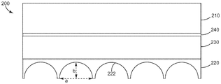
도 2는 시준 반사 편광기를 포함하는 광학 필름의 측단면도이다. 광학 필름(200)은 시준 반사 편광기(210), 렌즈릿(222)을 포함하는 마이크로렌즈 어레이(220), 광학 기재(230), 및 접착제(240)를 포함한다.2 is a side cross-sectional view of an optical film comprising a collimated reflective polarizer. The
시준 반사 편광기(210)는 임의의 적합한 두께일 수 있다. 일부 실시 형태에서, 시준 반사 편광기(210)는 다층 시준 반사 편광기일 수 있다. 다층 시준 반사 편광기의 경우, 층 두께 및 굴절률은 경사 입사광에 비해 축상(on-axis) 입사광의 더 양호한 투과율을 제공하기 위해 선택될 수 있다. 후방 반사체와 조합하여, 시준 반사 편광기는 경사 입사광을 재순환시킬 수 있다. 후속 통과에서, 재순환된 광은 축상에서 투과될 가능성이 더 커서, 시준 효과를 가져올 수 있다. 예를 들어, PCT 공개 WO 2013/059225 A1호(웨버 등)에 기재된 바와 같이, 이러한 필름을 사용한 재순환 백라이트로부터의 광의 잠재적인 시준도(degree of collimation)의 유용한 표시는 주어진 필름의 수직 입사(Tpassnormal) 및 60도 입사(Tpass60)에서의 투과된 p-편광된 광의 비로부터 얻어질 수 있다. 유용한 시준 반사 편광기는 Tpass60 대 Tpassnormal의 비가 0.75, 0.6, 0.5 이하보다 작을 수 있다.The collimated
마이크로렌즈 어레이(220)는 일련의 렌즈릿(222)을 포함한다. 마이크로렌즈 어레이(220) - 그의 라벨에도 불구하고 - 는 렌즈릿을 포함할 필요가 없지만, 그 대신에 또는 추가적으로 임의의 다른 미세특징부들, 예컨대 프리즘들 또는 구체들을 포함할 수 있다. 일부 실시 형태에서, 마이크로렌즈 어레이(220)의 미세특징부들이 반전되고; 즉, 특징부의 반전 형상이 렌즈릿(도 2에 도시된 바와 같음), 구체, 또는 프리즘이 된다. 일부 실시 형태에서, 미세특징부들은 하나의 평면내 방향으로 연장될 수 있고; 다시 말하면, 마이크로렌즈 어레이(220)는 1차원 어레이일 수 있다. 일부 실시 형태에서, 마이크로렌즈 어레이(220)는 2차원 어레이일 수 있다. 마이크로렌즈 어레이(220)는 규칙적으로, 임의로, 또는 의사 랜덤하게(pseudorandomly) 배열될 수 있고, 임의의 적합한 피치를 가질 수 있다. 일부 실시 형태에서, 렌즈릿(222)은 밀착하여 패킹되고; 일부 실시 형태에서, 렌즈릿(222)은 서로 이격되어 있다. 렌즈릿(222)은 마이크로렌즈 어레이(220) 상에 심지어 부분적으로 서로 겹칠 수 있다. 렌즈릿(222)은 2개의 특징 치수들: 그의 폭(a) 및 높이(또는 깊이)(b)를 포함한다. 렌즈릿(222)은 이러한 응용의 목적을 위해 b/a에 의해 주어지는 그의 종횡비에 의해 특징지어질 수 있다. 렌즈릿(222)은 적어도 하나의 만곡된 표면을 포함할 수 있다. 일부 실시 형태에서, 렌즈릿(222)은 만곡된 표면만을 포함할 수 있다. 도 2에 도시된 바와 같은 렌즈릿(222)은, 적어도 이러한 응용의 목적을 위해 오목한 미세특징부라고 간주되고 오목한 미세특징부로 지칭될 수 있다.The
렌즈릿(222)의 종횡비는 적절한 광학 특성을 갖는 적층물을 설계함에 있어서 중요할 수 있다. 종횡비는 어떤 경우에 시준 효과와 확산 사이의 트레이드오프(tradeoff)일 수 있다. 예를 들어, 렌즈릿에 대해, 비교적 높은 종횡비는 더 적은 시준 효과를 제공하는 한편 비교적 더 양호한 확산을 제공할 수 있다. 일부 실시 형태에서, 약 0.5의 종횡비가 적합하다. 일부 실시 형태에서, 0.5 미만, 예를 들어, 약 0.3의 종횡비가 적합하다. 마이크로렌즈 어레이(220) 내의 개별 렌즈릿은 정상적인 제조 변동성을 넘어서는 종횡비의 변동을 가질 수 있다. 그러한 경우에, 평균 종횡비는 0.5 미만, 또는 임의의 다른 적합한 값일 수 있다.The aspect ratio of the
마이크로렌즈 어레이(220)는 주조 및 경화와 같은 미세복제 공정을 비롯한 임의의 적합한 공정을 통해 형성될 수 있다. 마이크로렌즈 어레이(220)를 형성하기 위해 사용되는 수지는 그의 처리 능력, 내구성, 용융 및 휨 내성(warp resistance)과 같은 다른 물리적 특성, 및 굴절률, 투명성 및 확산 품질과 같은 광학 특성을 위해 선택될 수 있다. 일부 실시 형태에서, 마이크로렌즈 어레이(220)의 렌즈릿(222) 사이의 영역은 인접한 필름의 잠재적인 긁힘을 감소시키기 위해 둥글거나, 사각형이거나, 또는 달리 변형될 수 있다.The
광학 기재(230)가 시준 반사 편광기(210)와 마이크로렌즈 어레이(220) 사이에 배치된다. 일부 실시 형태에서, 마이크로렌즈 어레이(220)는 광학 기재(230) 상으로 직접 미세복제된다. 광학 기재(230) 및 마이크로렌즈 어레이(220)는 동일한 재료일 수 있고, 일부 실시 형태에서, 그들은 동일한 단일체 재료 조각의 일부일 수 있다. 다른 실시 형태에서, 광학 기재(230)는 마이크로렌즈 어레이(220)에 접착되거나 또는 적층될 수 있다. 광학 기재는 폴리에틸렌 테레프탈레이트(PET), 폴리카르보네이트(PC) 또는 폴리(메틸 메타크릴레이트)(PMMA)와 같은 중합체 재료를 비롯한 임의의 적합한 재료일 수 있다. 광학 기재(230)는 임의의 적합한 두께를 비롯한 임의의 적합한 치수일 수 있다. 일부 실시 형태에서, 적합한 강성을 제공하기 위해 적절한 두께가 선택될 수 있다. 일부 실시 형태에서, 광학 기재(230)는 마이크로렌즈 어레이(220)와 시준 반사 편광기(210) 사이에 적합한 광학 경로 길이를 제공하도록 선택된 그의 두께를 가질 수 있다. 광학 기재(230)는 실질적으로 투명하고 광학적으로 불활성일 수 있거나, 또는 그것은, 벌크 확산기가 되는 것, 또는 흡수 편광 요소들 또는 염료들을 포함하는 것과 같이 광학 기능을 가질 수 있다.An
접착제(240)가 시준 반사 편광기(210)와 광학 기재(230) 사이에 선택적으로 배치된다. 접착제(240)는 광학적으로 투명한 접착제(optically clear adhesive, OCA), 감압 접착제(pressure sensitive adhesive, PSA), 또는 열 또는 UV-경화성 접착제를 비롯한 임의의 적합한 접착제일 수 있다. 일부 실시 형태에서, 접착제(240)는 광학적으로 불활성인, 즉 투명한 것이 바람직할 수 있다. 다른 실시 형태에서, 접착제(240)는 안료, 확산 입자, 또는 광학 필름(200)을 통하여 이동하는 광을 변경 또는 변형시키는 다른 광학 활성 성분을 포함할 수 있다.An adhesive 240 is selectively disposed between the collimated
도 2에 도시된 광학 필름(200)의 전체 구성은 임의의 적합한 크기의 것일 수 있고, 임의의 적합한 치수를 가질 수 있다. 일부 실시 형태에서, 광학 필름(200)의 층들은 동일한 크기의 것일 수 있고, 심지어 롤 형태로 제조되거나 저장되어, 원하는 크기의 부분품들로 변환될 수 있다. 일반적으로, 광학 필름(200)은 2개의 외부 표면들: 시준 반사 편광기(210)에 인접한 제1 표면, 및 마이크로렌즈 어레이(220)에 인접한 제2 표면을 갖는다. 광학 필름(200)은 다른 필름 및 광학 구성요소, 예컨대 시준 반사 편광기(210)에 인접한 제1 외부 표면에 부착되는 확산기, 흡수 편광기, 또는 터닝 필름(turning film)을 포함할 수 있다.The overall configuration of the
오목 마이크로렌즈 어레이는 일반적으로 재순환 백라이트에서의 반사 편광기와 함께 사용되지 않는다. 특히, 오목 마이크로렌즈 어레이는 백라이트 효율의 관점에서 너무 강하고 바람직하지 않은 확산 효과를 갖는다고 생각되었다. 그러나, 출원인은 의외로, 오목 마이크로렌즈 어레이가, 시준 반사 편광기와 조합하여, 백라이트 결함 은폐를 위한 적절한 확산을 갖는 원하는 전체 시준 효과를 제공할 수 있음을 발견하였다. 이것은 백라이트 설계의 더 큰 유연성을 허용하고, 표준 백라이트 재순환 공동처럼 필적하는 또는 우수한 성능을 갖는 더 얇은 구성을 가능하게 한다. 또한, 더 얇은 베이스 구성은 허용가능한 전체 두께를 보존하면서 백라이트 내에 더 많은 광학 특징부들, 구성요소들 또는 층들을 부여함에 있어서의 설계 유연성을 가능하게 한다.Concave microlens arrays are generally not used with reflective polarizers in recirculating backlights. In particular, it has been thought that the concave microlens array is too strong and has an undesirable diffusion effect in terms of backlight efficiency. However, Applicants have surprisingly found that concave microlens arrays can, in combination with collimated reflective polarizers, provide the desired overall collimation effect with proper diffusion for backlight defect concealment. This allows for greater flexibility of the backlight design and enables a thinner configuration that matches or performs as well as a standard backlight recirculating cavity. A thinner base configuration also allows design flexibility in imparting more optical features, components, or layers into the backlight while preserving the total allowable thickness.
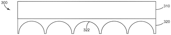
도 3은 시준 반사 편광기를 포함하는 다른 광학 필름의 측단면도이다. 광학 필름(300)은 시준 반사 편광기(310), 및 렌즈릿(322)을 포함하는 마이크로렌즈 어레이(320)를 포함한다. 도 3은, 도 2의 광학 필름(200)에 일반적으로 대응하지만, 마이크로렌즈 어레이(320)가 시준 반사 편광기(310) 상에 직접 미세복제되거나 또는 달리 형성된, 광학 필름의 대안적인 구성을 도시한다.3 is a side cross-sectional view of another optical film comprising a collimated reflective polarizer. The
광학 필름(300)은 광학 기재를 포함하지 않기 때문에 자연스럽게 더 얇은 구성일 수 있다. 박형화(thinness)는 핸드헬드 및 모바일 디스플레이를 비롯한 일부 응용에서 바람직할 수 있다. 그 외에, 마이크로렌즈 어레이(320) 및 시준 반사 편광기(310)의 선택 및 설계는 도 2의 대응하는 요소들(210, 220)에 대해 전술한 것과 동일한 고려사항 및 특징부를 고려할 수 있다.The
도 4는 시준 반사 편광기를 포함하는 다른 광학 필름의 측단면도이다. 광학 필름(400)은 비드들(412A), 프리즘들(412B) 및 렌즈들(412C)을 포함하는 시준 반사 편광기(410), 렌즈릿(422)을 포함한 마이크로렌즈 어레이(420), 광학 기재(430), 및 접착제(440)를 포함한다. 도 4의 광학 필름(400)은 대체로 도 2의 광학 필름(200)에 대응하지만, 도 4는 소정의 실시 형태에 대해 제공될 수 있는 다양한 상부 표면 미세구조물들 및 미세특징부들을 예시한다.4 is a side cross-sectional view of another optical film comprising a collimated reflective polarizer. The
비드들(412A)은 시준 반사 편광기(410)에 인접한 표면 상에 배치될 수 있고, 여러 기능들을 수행할 수 있다. 일부 실시 형태에서, 비드들(412A)은 웨트아웃 방지(anti-wetout), 반사 방지, 또는 뉴턴링 방지(anti-Newton ring) 층으로서 기능할 수 있다. 원하는 기능에 기초한 적절한 비드 크기 및 밀도는 당업자들에게 명백할 것이다. 일부 실시 형태에서, 8 μm 비드들(평균 직경이 8 μm인 비드들)이 사용될 수 있다. 일부 실시 형태에서, 더 작은 비드들, 심지어 1 μm 이하 정도로 작은 비드들이 적절할 수 있다. 비드들은 결합제 또는 용액 또는 용매에 침착될 수 있는데, 어떤 경우에는 비드들이 광학 필름(400)의 표면 상에 배치되거나 또는 그에 접착된 채로 증발될 수 있다. 비드들(412A)은 또한 시준 반사 편광기(410)에 대한 긁힘 내성 또는 보호를 제공할 수 있다. 비드들(412A)은 투명하거나 불투명할 수 있고, 임의의 적합한 재료의 것일 수 있다.
본 명세서에 기술된 광학 필름의 실시 형태에서 가능한 다양한 표면 구조들을 입증하기 위해 프리즘들(412B) 및 렌즈들(412C)이 광학 필름(400) 상에 도시되어 있다. 프리즘들(412B)은, 예를 들어, 광을 추가로 시준하기 위해 유용할 수 있다. 이러한 미세특징부들의 임의의 적합한 피치 및 배열이 광학 필름(400)과 함께 고려된다. 도 4가 설명의 편의상 동일한 광학 필름 상에 비드들(412A), 프리즘들(412B) 및 렌즈들(412C)을 도시하고 상이한 미세특징부들의 개별 섹션들을 필연적으로 제시하도록 의도되지 않지만, 일부 실시 형태에서는 하나 초과의 유형의 미세특징부가 광학 필름(400) 상에 배치될 수 있다.The
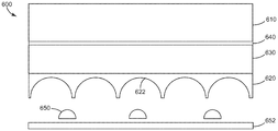
도 5는 도 2의 광학 필름을 포함하는 에지형 백라이트의 일부분의 측단면도이다. 광학 적층물(500)은 시준 반사 편광기(510), 렌즈릿(522)을 포함하는 마이크로렌즈 어레이(520), 광학 기재(530), 접착제(540), 하나 이상의 광원들(550), 반사체(552), 및 도광체(554)를 포함한다.5 is a side cross-sectional view of a portion of an edge-type backlight including the optical film of Fig. The
광학 적층물(500)은 시준 반사 편광기(510), 렌즈릿(522)을 포함하는 마이크로렌즈 어레이(520), 광학 기재(530), 및 접착제(540)를 포함하는, 도 2의 광학 필름(200)에 본질적으로 대응하는 광학 필름을 나타낸다. 또한, 광학 적층물(500)은 하나 이상의 광원들(550), 반사체(552), 및 도광체(554)를 포함한다.The
하나 이상의 광원들(550), 반사체(552), 및 도광체(554)의 구성은 에지형 시스템을 대표한다. 이러한 시스템에서, 하나 이상의 광원들(550)로부터 광이 주입되고 도광체(554)에 들어간다. 하나 이상의 광원들(550)로부터 도광체(554)로의 광의 주입은 주입 또는 시준 광학계를 이용할 수 있다. 광은 하나 이상의 계면들에서의 내부 전반사를 통하여 도광체(554) 내에서 전송된다. 도 5에서, 도광체(554)의 상부 표면은 공기에 노출되어 있는 것으로 도시되어 있다. 임계 각도(주지된 스넬의 법칙(Snell's law)으로부터 계산됨) 초과의 각도로 도광체/공기 계면에 입사하는 광은 내부 전반사된다. 반사체(552)는 또한 광을 전송하는 역할을 하고, 경면 또는 반경면 반사될 수 있다. 일부 실시 형태에서, 도광체(554), 반사체(552), 또는 둘 모두는 확산 또는 추출 특징부들을 포함할 수 있는데, 확산 또는 추출 특징부들은 전송된 광을 도광체(554)로부터 분리시키는 것을 돕고 그것이 임계 각도 미만으로 도광체/공기 계면에 입사하도록 한다. 이러한 방식으로, 하나 이상의 광원들(550)로부터의 광은 도 2와 관련하여 기술된 광학 필름(200)과 동등한 필름을 포함하는 광학 적층물(500)의 부분에 입사하게 된다. 시준 반사 편광기(510)에 의해 반사될 수 있는 광이 도광체(554)를 통해 다시 하방으로 반사되고, 광학 필름을 향해 다시 상방으로 반사되기 전에 반사체(552)에 입사된다. 이러한 방식으로, 광이 달리 사용가능하지 않거나 바람직하지 않은 시야각으로 (궁극적인 백라이트 또는 관찰 디바이스로부터) 발광될 수 있거나 또는 백라이트 내의 다른 구성요소들에 의해 흡수될 수 있을 때, 광은 보다 사용가능한 편광 상태 또는 입사각으로 재순환된다.The configuration of the one or more
하나 이상의 광원들(550)은 CCFL, LED, 백열 전구, 또는 이들의 임의의 조합을 포함하여, 임의의 개수의 광원들일 수 있다. 일부 실시 형태에서, 하나 이상의 광원들(550)은 제한된 범위의 파장들에 걸쳐 발광할 수 있고, 일부 실시 형태에서, 하나 이상의 광원들의 상이한 광원들은 상이한 파장 범위들에 걸쳐 발광할 수 있다. 일부 실시 형태에서, 하나 이상의 광원들(550)은 실질적으로 백색 광을 발광할 수 있다. 하나 이상의 광원들(550)이 LED를 포함하는 실시 형태에서, 하나 이상의 광원들(550)은 실질적으로 램버트(Lambertian) 분포의 광을 발광할 수 있다.The one or more
도광체(554)는 임의의 적합한 재료로 구성될 수 있고, 임의의 적합한 형상 또는 크기의 것일 수 있다. 예를 들어, 도광체는 아크릴로 형성될 수 있고, 평면이거나, 테이퍼지거나 또는 만곡될 수 있다. 반사체(552)는 임의의 적합한 반사체일 수 있다. 일부 실시 형태에서, 반사체(552)는 다층 반사 필름, 예컨대 미국 미네소타주 세인트 폴 소재의 쓰리엠 컴퍼니(3M Company)로부터 입수가능한 향상된 경면 반사체(Enhanced Specular Reflector, ESR)일 수 있다.The
광학 적층물(500)은 마이크로렌즈 어레이(520)가 도광체(554)에 근접해 있도록 배향된다. 예를 들어, 하나 이상의 광원들(550) 및 렌즈릿(522) 또는 도광체(554) 및 시준 반사 편광기(510)의 예시된 상대적 크기들은 설명을 용이하게 하기 위함이고, 그러한 구성요소들의 실제 상대적 치수들을 제안하기 위함이라고 이해되지 않아야 한다.The
도 6은 도 2의 광학 필름을 포함하는 직하형 백라이트의 일부분의 측단면도이다. 광학 적층물(600)은 시준 반사 편광기(610), 렌즈릿(622)을 포함하는 마이크로렌즈 어레이(620), 광학 기재(630), 접착제(640), 하나 이상의 광원들(650), 및 반사체(652)를 포함한다.Fig. 6 is a side cross-sectional view of a portion of a direct-type backlight including the optical film of Fig. 2; The
광학 적층물(600)은 시준 반사 편광기(610), 렌즈릿(622)을 포함하는 마이크로렌즈 어레이(620), 광학 기재(630), 및 접착제(640)를 포함하는, 도 2의 광학 필름(200)에 본질적으로 대응하는 광학 필름을 나타낸다. 또한, 광학 적층물(600)은 하나 이상의 광원들(650) 및 반사체(652)를 포함한다.The
하나 이상의 광원들(650) 및 반사체(652)의 구성은 직하형 백라이트를 대표한다. 이러한 시스템에서, 도광체는 일반적으로 사용되지 않는다 - 그 대신에, 하나 이상의 광원들로부터의 광은 도 6에서, 예를 들어, 도 2의 광학 필름(200)에 대응하는 광학 필름에 직접 입사된다. 이러한 경우에, 광원들이 충분히 확산되지 않는 경우 밝은 점들이 있을 수 있다. 광이 광학 필름에 입사된다. 시준 반사 편광기(610)에 의해 반사된 광은 반사체(652)로 다시 반사되고, 이어서 광학 필름을 향해 다시 지향된다. 도 6의 구성에서와 같이, 광은 이러한 백라이트 공동 내에서 재순환된다. 마이크로렌즈 어레이(620)는 하나 이상의 광원들(650)에 근접해 있도록 구성된다.The configuration of the one or more
예Yes
비교예 C-1Comparative Example C-1
탁도가 7%인 비드형(beaded) PET 확산기 필름의 상부 상에 배치된 프리즘 필름(320 마이크로미터 BEF)의 상부 상에 반사 편광기(DBEF-D2-400)를 배치함으로써 필름 적층물을 제조하였다(모두 미국 미네소타주 세인트 폴 소재의 쓰리엠 컴퍼니로부터 입수가능함). 확산기 층이 백라이트에 가장 가까운 상태로 백라이트 필름으로서 필름을 시험하였다. 이득은 미국 캘리포니아주 채츠워스 소재의 포토 리서치 인크.(Photo Research, Inc.)로부터 입수가능한 스펙트라스캔(SPECTRASCAN) PR-650을 사용하여 측정하였다. 탁도는 헤이즈-가드 플러스(HAZE-GARD PLUS) 4725 탁도 측정기(미국 메릴랜드주 실버 스프링스 소재의 비와이케이-가드너(BYK-Gardner)로부터 입수가능함)를 사용하여 측정하였다. 축상 휘도는 엘딤 이제트 콘트라스트(ELDIM EZ CONTRAST) 160R(프랑스 소재의 엘딤 코포레이션(ELDIM Corp.)으로부터 입수가능함)를 사용하여 측정하였다. 결과가 표 1에 주어져 있다. 확산기 층이 백라이트에 가장 가까운 상태로 필름 적층물을 LED 백라이트 위에 배치하였고, 필름이 LED들을 은폐할 수 있는 정도를 시각적으로 평가하였다. 필름 적층물이 양호한 핫 스폿(hot spot) 은폐를 제공했음을 알아냈다.A film laminate was prepared by placing a reflective polarizer (DBEF-D2-400) on top of a prism film (320 micrometer BEF) placed on top of a beaded PET diffuser film with a turbidity of 7% All available from 3M Company, St. Paul, Minn.). The film was tested as a backlight film with the diffuser layer closest to the backlight. The gain was measured using SPECTRASCAN PR-650, available from Photo Research, Inc., Chatsworth, CA. The turbidity was measured using a HAZE-GARD PLUS 4725 turbidity meter (available from BYK-Gardner, Silver Springs, MD). The axial brightness was measured using ELDIM EZ CONTRAST 160R (available from ELDIM Corp., France). The results are given in Table 1. The film laminate was placed on the LED backlight with the diffuser layer closest to the backlight, and the degree to which the film was able to conceal the LEDs was visually evaluated. It has been found that the film stack provided a good hot spot concealment.
비교예 C-2Comparative Example C-2
본 명세서에 참고로 포함된 PCT 특허 출원 US 2012/060485호의 실시예 3에 기재된 바와 같이 시준 다층 광학 필름(collimating multilayer optical film, CMOF)을 제조하였다. 특히, 2011년 5월 6일자로 출원된, 발명의 명칭이 "다층 중합체 필름을 제조하기 위한 피드블록(Feedblock for Manufacturing Multilayer Polymeric Films)"인 미국 특허 출원 공개 제2011/0272849호에 기재된 피드블록 방법을 이용하여, 교호하는 저 굴절률 및 고 굴절률 중합체 층들로 된 275개 층들을 각각 갖는 2개의 패킷들을 캐스트 웨브로서 공압출하고 나서, 연속 필름 제조 라인의 텐터(tenter)에서 연신시켰다. 고 굴절률 재료는 90/10 coPEN(90% 나프탈레이트 유닛 및 10% 테레프탈레이트 유닛)이었다. 저 굴절률 재료는 미세층들의 패킷 1과 패킷 2 사이에서 상이하였다. 패킷 1을 위한 저 굴절률 재료는 PETg(미국 테네시주 킹즈포트 소재의 이스트만 케미칼(Eastman Chemical)로부터의 이스타(EASTAR) GN071 코폴리에스테르)와 비정질 55/45 coPEN(55% 나프탈레이트 유닛 및 45% 테레프탈레이트 유닛)의 블렌드였다. 1.589의 굴절률을 얻도록 블렌드 비를 조절하였다. 패킷 2를 위한 저 굴절률 재료는 이스트만 케미칼(미국 테네시주 킹즈포트 소재)로부터의 트리탄(TRITAN) FX150 코폴리에스테르였고, 1.554의 측정된 굴절률을 가졌다. 모든 굴절률을 633 nm에서 측정하였다.A collimating multilayer optical film (CMOF) was prepared as described in Example 3 of PCT patent application US 2012/060485, incorporated herein by reference. In particular, the feedblock method described in U.S. Patent Application Publication No. 2011/0272849, filed May 6, 2011, entitled " Feedblock for Manufacturing Multilayer Polymeric Films " , Two packets each having 275 layers of alternating low and high refractive index polymer layers were coextruded as a cast web and then stretched in a tenter of a continuous film production line. The high refractive index material was 90/10 coPEN (90% naphthalate unit and 10% terephthalate unit). The low refractive index material was different between Packet 1 and Packet 2 of the microlayers. The low refractive index material for Packet 1 was PETg (EASTAR GN071 copolyester from Eastman Chemical, Tennessee, USA) and amorphous 55/45 coPEN (55% naphthalate unit and 45% Phthalate unit). The blend ratio was adjusted to obtain a refractive index of 1.589. The low refractive index material for Packet 2 was TRITAN FX150 copolyester from Eastman Chemical, Kingsport, Tenn., And had a measured index of refraction of 1.554. All refractive indices were measured at 633 nm.
CMOF 필름의 층 두께 값들은 원자력 현미경(Atomic Force Microscopy, AFM)을 사용하여 측정하였고, 패킷 1 및 패킷 2 각각에 대한 층 두께 프로파일들(13a, 13b)이 도 7에 도시되어 있다.The layer thickness values of the CMOF film were measured using Atomic Force Microscopy (AFM) and the
0도에서의 투과율 값에 대한 60도로 투과된 통과 축 광의 비는 재순환 백라이트와 함께 사용될 때 필름의 시준 잠재성의 양호한 표시이다. p-편광된 입사광 및 s-편광된 입사광에 대한 투과율 스펙트럼들을 0도 및 60도의 입사각들에 대해 결정하였다. 각각의 측정에 대한 평균 투과율 값들(%T)을 420 nm 내지 680 nm의 각각의 스펙트럼의 투과율 값들을 평균함으로써 추정하였다. 명소시 가중치(photopic weighting)를 사용하지 않았지만, 원한다면 이것이 적용될 수 있다. CMOF 필름에 대한 평균 %T 값들은 다음과 같았다: p-편광에 대해 0도에서의 75%로부터 60도에서의 46%로 떨어지고, s-편광에 대해 0도에서의 75%로부터 60도에서의 36%로 떨어진다. p-편광된 광 및 s-편광된 광에 대한 Tpass60/Tpassnormal의 값들의 비들은 각각 0.62 및 0.48이었다.The ratio of pass-through light transmitted at 60 degrees to the transmittance value at 0 degrees is a good indication of the collimation potential of the film when used with the recirculating backlight. The transmittance spectra for p-polarized incident light and s-polarized incident light were determined for incident angles of 0 and 60 degrees. The average transmittance values (% T) for each measurement were estimated by averaging the transmittance values of each spectrum of 420 nm to 680 nm. We did not use photopic weighting, but this can be applied if desired. The average% T values for the CMOF film were: 75% at 0 degrees for p-polarization falling to 46% at 60 degrees, and 75% at 0 degrees for s- 36%. The ratios of the values of Tpass60 / Tpassnormal for p-polarized light and s-polarized light were 0.62 and 0.48, respectively.
이득, 탁도 및 휘도는 비교예 C-1에서와 같이 결정되었고, 표 1에 기록되어 있다. 필름이 LED들을 은폐할 수 있는 정도를 비교예 C-1에서와 같이 평가하였고, 매우 부족하다는 것을 알아냈다.The gain, turbidity, and luminance were determined as in Comparative Example C-1 and are listed in Table 1. The degree to which the film can conceal the LEDs was evaluated as in comparative example C-1 and found to be very poor.
비교예 C-3Comparative Example C-3
CMOF 필름을 비교예 C-2에서와 같이 제조하였고, 비드형 확산기 층(비드 코팅된 188 마이크로미터 두께의 7% 탁도를 갖는 PET 필름, 상표명 CH003U0로 에스케이씨 하스 디스플레이 필름즈(SKC Haas Display Films)(한국 서울 소재)로부터 입수가능함)을 CMOF에, 비드 측이 CMOF를 등지는 상태로 OCA 8171 CL(미국 미네소타주 세인트 폴 소재의 쓰리엠 컴퍼니로부터 입수가능한 광학적으로 투명한 접착제)을 사용하여 부착하였다. 비드형 층이 백라이트에 가장 가까운 상태로 백라이트 필름으로서 필름을 시험하였다. 이득, 탁도 및 휘도는 비교예 C-1에서와 같이 결정되었고, 표 1에 기록되어 있다. 필름이 LED들을 은폐할 수 있는 정도를 비교예 C-1에서와 같이 평가하였고, 부족하다는 것을 알아냈다.A CMOF film was prepared as in Comparative Example C-2, and a bead spreader layer (bead coated PET film with 7% turbidity of 188 micrometer thickness, trade name CH003U0 by SKC Haas Display Films ( Seoul, Korea) was attached to CMOF and the bead side was attached using OCA 8171 CL (optically transparent adhesive available from 3M Company, St. Paul, MN, USA) with CMOF back. The film was tested as a backlight film with the bead-like layer closest to the backlight. The gain, turbidity, and luminance were determined as in Comparative Example C-1 and are listed in Table 1. The degree to which the film can conceal the LEDs was evaluated as in Comparative Example C-1 and found to be inadequate.
실시예 1Example 1
CMOF 필름을 비교예 C-1에서와 같이 제조하였다. 오목 마이크로렌즈들을 일 표면 상에 갖는 PET 필름을 엠엔테크 코포레이션(MNTech Corporation)(한국 서울 소재)으로부터 획득하였다. 마이크로렌즈들은 피치가 약 30 마이크로미터였고, 높이가 약 10 마이크로미터였다. 마이크로렌즈 필름을 CMOF 필름에, 마이크로렌즈 측이 CMOF를 등지는 상태로 OCA 8171 CL(미국 미네소타주 세인트 폴 소재의 쓰리엠 컴퍼니로부터 입수가능함)을 사용하여 적층하였다. 마이크로렌즈 층이 백라이트에 가장 가까운 상태로 백라이트 필름으로서 필름을 시험하였다. 이득, 탁도 및 휘도는 비교예 C-1에서와 같이 결정되었다. 필름이 LED들을 은폐할 수 있는 정도를 비교예 C-1에서와 같이 평가하였고, 양호한 핫 스폿 은폐를 제공한다는 것을 알아냈다.A CMOF film was prepared as in Comparative Example C-1. A PET film having concave microlenses on one surface was obtained from MNTech Corporation (Seoul, Korea). The microlenses had a pitch of about 30 micrometers and a height of about 10 micrometers. The micro-lens film was laminated to the CMOF film and the micro lens side was laminated using OCA 8171 CL (available from 3M Company, St. Paul, MN, USA) with the CMOF back. The film was tested as a backlight film with the microlens layer closest to the backlight. The gain, turbidity and luminance were determined as in Comparative Example C-1. The degree to which the film can conceal the LEDs was evaluated as in Comparative Example C-1 and found to provide good hotspot concealment.
실시예 2Example 2
마이크로렌즈들의 피치가 약 50 마이크로미터이고 높이가 약 25 마이크로미터인 것 이외에는 실시예 1에서와 동일하게 필름을 제조하였다. 마이크로렌즈 층이 백라이트에 가장 가까운 상태로 백라이트 필름으로서 필름을 시험하였다. 이득, 탁도 및 휘도는 비교예 C-1에서와 같이 결정되었다. 필름이 LED들을 은폐할 수 있는 정도를 비교예 C-1에서와 같이 평가하였고, 양호한 핫 스폿 은폐를 제공한다는 것을 알아냈다.A film was prepared in the same manner as in Example 1, except that the microlenses had a pitch of about 50 micrometers and a height of about 25 micrometers. The film was tested as a backlight film with the microlens layer closest to the backlight. The gain, turbidity and luminance were determined as in Comparative Example C-1. The degree to which the film can conceal the LEDs was evaluated as in Comparative Example C-1 and found to provide good hotspot concealment.
[표 1][Table 1]

하기는 본 발명에 따른 예시적인 실시 형태이다.The following is an exemplary embodiment according to the present invention.
항목 1.Item 1.
시준 반사 편광기; 및Collimated reflective polarizer; And
시준 반사 편광기의 주 표면 상에 배치되는 오목 마이크로렌즈들의 어레이를 포함하는, 광학 필름.And an array of concave microlenses disposed on a major surface of the collimated reflective polarizer.
항목 2.Item 2.
제1 및 제2 주 표면을 갖는 광학 기재;An optical substrate having a first and a second major surface;
광학 기재의 제1 주 표면 상에 배치되는 시준 반사 편광기; 및A collimated reflective polarizer disposed on a first major surface of an optical substrate; And
광학 기재의 제2 주 표면 상에 배치되는 오목 마이크로렌즈들의 어레이를 포함하는, 광학 필름.And an array of concave microlenses disposed on a second major surface of the optical substrate.
항목 3. 광학 기재와 시준 반사 편광기 사이에 접착제를 추가로 포함하는, 항목 2의 광학 필름.Item 3. The optical film of item 2, further comprising an adhesive between the optical substrate and the collimated polarizer.
항목 4. 시준 반사 편광기는 p-편광된 광에 대해 수직 입사에서 통과 축을 따른 투과율이 Tpassnormal이고 p-편광된 광에 대해 60도 입사에서 통과 축을 따른 투과율이 Tpass60이고, Tpass60 대 Tpassnormal의 비가 0.75 미만인, 항목 1 또는 항목 2의 광학 필름.Item 4. A collimated reflective polarizer has a transmittance Tpassnormal along the pass axis at normal incidence for p-polarized light and a transmittance Tpass60 along the pass axis at 60 degrees incident for p-polarized light with a Tpass60 to Tpassnormal ratio of less than 0.75 , Item 1 or item 2 of the optical film.
항목 5. Tpass60 대 Tpassnormal의 비가 0.60 미만인, 항목 4의 광학 필름.Item 5. The optical film of item 4, wherein the ratio of
항목 6. Tpass60 대 Tpassnormal의 비가 0.50 미만인, 항목 5의 광학 필름.Item 6. The optical film of item 5, wherein the ratio of
항목 7. 오목 마이크로렌즈들의 어레이가 임의로 배열되는, 항목 1 또는 항목 2의 광학 필름.Item 7. The optical film of item 1 or item 2, wherein the array of concave microlenses is arbitrarily arranged.
항목 8. 오목 마이크로렌즈들의 어레이가 규칙적으로 배열되는, 항목 1 또는 항목 2의 광학 필름.Item 8. The optical film of item 1 or item 2, wherein the array of concave microlenses is regularly arranged.
항목 9. 오목 마이크로렌즈들의 어레이에서의 각각의 마이크로렌즈는 종횡비가 약 0.5인, 항목 1 또는 항목 2의 광학 필름.Item 9. The optical film of item 1 or item 2, wherein each microlens in the array of concave microlenses has an aspect ratio of about 0.5.
항목 10. 오목 마이크로렌즈들의 어레이에서의 각각의 마이크로렌즈는 종횡비가 약 0.3인, 항목 9의 광학 필름.
항목 11. 오목 마이크로렌즈들의 어레이에서의 각각의 마이크로렌즈는 종횡비가 약 0.5 미만인, 항목 1 또는 항목 2의 광학 필름.Item 11. The optical film of item 1 or item 2, wherein each microlens in the array of concave microlenses has an aspect ratio of less than about 0.5.
항목 12. 오목 마이크로렌즈들의 어레이 상에 배치되지 않는 시준 반사 편광기의 표면 상에 배치되는 미세특징부들을 추가로 포함하는, 항목 1의 광학 필름.
항목 13. 광학 기재 상에 배치되지 않는 시준 반사 편광기의 표면 상에 배치되는 미세특징부들을 추가로 포함하는, 항목 2의 광학 필름.Item 13. The optical film of item 2, further comprising fine features disposed on a surface of a collimated reflective polarizer that is not disposed on the optical substrate.
항목 14. 미세특징부들이 비드들을 포함하는, 항목 12 또는 항목 13의 광학 필름.
항목 15. 비드들의 평균 직경이 약 8 μm인, 항목 14의 광학 필름.Item 15. The optical film of
항목 16. 미세특징부들이 볼록 렌즈들을 포함하는, 항목 12 또는 항목 13의 광학 필름.Item 16. The optical film of
항목 17. 미세특징부들이 프리즘들을 포함하는, 항목 12 또는 항목 13의 광학 필름.Item 17. The optical film of
항목 18. 광학 필름은 두께가 420 μm 미만인, 항목 1 또는 항목 2의 광학 필름.Item 18. The optical film of item 1 or item 2, wherein the optical film has a thickness of less than 420 μm.
항목 19.Item 19.
항목 1 또는 항목 2의 광학 필름; 및Item 1 or item 2 optical film; And
도광체를 포함하고,A light guide,
도광체는 오목 마이크로렌즈들의 어레이에 근접하여 배치되는, 에지형 백라이트 조립체.Wherein the light guide is disposed in close proximity to the array of concave microlenses.
항목 20.Item 20.
항목 1 또는 항목 2의 광학 필름; 및Item 1 or item 2 optical film; And
하나 이상의 광원들을 포함하고,Comprising one or more light sources,
하나 이상의 광원들은 오목 마이크로렌즈들의 어레이에 근접하여 배치되는, 직하형 백라이트 조립체.Wherein the at least one light source is disposed close to the array of concave microlenses.
도면에서의 요소에 대한 설명은, 달리 표시되지 않는다면, 다른 도면에서의 대응하는 요소에 동일하게 적용하는 것으로 이해되어야 한다. 본 발명은 전술한 특정 실시 형태들로 제한되는 것으로 간주되어서는 안 되는데, 그 이유는, 본 발명의 다양한 태양들의 설명을 용이하게 하기 위하여 그러한 실시 형태들이 상세히 기술되어 있기 때문이다. 오히려, 본 발명은 첨부된 청구범위 및 그 등가물들에 의해 한정되는 본 발명의 범주 내에 속하는 다양한 변형들, 등가의 공정들, 및 대안적인 디바이스들을 포함한 본 발명의 모든 태양들을 포함하는 것으로 이해되어야 한다.The description of the elements in the drawings should be understood to apply equally to the corresponding elements in the other drawings unless otherwise indicated. The present invention should not be construed as limited to the specific embodiments described above because such embodiments are described in detail in order to facilitate describing the various aspects of the invention. Rather, the invention is to be understood as embracing all forms of the invention including various modifications, equivalent processes, and alternative devices that fall within the scope of the invention as defined by the appended claims and equivalents thereof .
Claims (10)
시준 반사 편광기의 주 표면 상에 배치되는 오목 마이크로렌즈들의 어레이를 포함하는, 광학 필름.Collimated reflective polarizer; And
And an array of concave microlenses disposed on a major surface of the collimated reflective polarizer.
광학 기재의 제1 주 표면 상에 배치되는 시준 반사 편광기; 및
광학 기재의 제2 주 표면 상에 배치되는 오목 마이크로렌즈들의 어레이를 포함하는, 광학 필름.An optical substrate having a first and a second major surface;
A collimated reflective polarizer disposed on a first major surface of an optical substrate; And
And an array of concave microlenses disposed on a second major surface of the optical substrate.
도광체를 포함하고,
도광체는 오목 마이크로렌즈들의 어레이에 근접하여 배치되는, 에지형(edge-lit) 백라이트 조립체.An optical film according to claim 1 or 2; And
A light guide,
Wherein the light guide is disposed in close proximity to the array of concave microlenses.
하나 이상의 광원들을 포함하고,
하나 이상의 광원들은 오목 마이크로렌즈들의 어레이에 근접하여 배치되는, 직하형(direct-lit) 백라이트 조립체.An optical film according to claim 1 or 2; And
Comprising one or more light sources,
Wherein the at least one light source is disposed close to an array of concave microlenses.
Applications Claiming Priority (3)
| Application Number | Priority Date | Filing Date | Title |
|---|---|---|---|
| US201361921802P | 2013-12-30 | 2013-12-30 | |
| US61/921,802 | 2013-12-30 | ||
| PCT/US2014/071669 WO2015102961A1 (en) | 2013-12-30 | 2014-12-19 | Optical film including collimating reflective polarizer |
Publications (1)
| Publication Number | Publication Date |
|---|---|
| KR20160105442A true KR20160105442A (en) | 2016-09-06 |
Family
ID=52355239
Family Applications (1)
| Application Number | Title | Priority Date | Filing Date |
|---|---|---|---|
| KR1020167020406A KR20160105442A (en) | 2013-12-30 | 2014-12-19 | Optical film including collimating reflective polarizer |
Country Status (6)
| Country | Link |
|---|---|
| US (2) | US11156756B2 (en) |
| JP (1) | JP2017509931A (en) |
| KR (1) | KR20160105442A (en) |
| CN (1) | CN105849595B (en) |
| TW (1) | TW201537231A (en) |
| WO (1) | WO2015102961A1 (en) |
Families Citing this family (19)
| Publication number | Priority date | Publication date | Assignee | Title |
|---|---|---|---|---|
| GB2484713A (en) | 2010-10-21 | 2012-04-25 | Optovate Ltd | Illumination apparatus |
| CN105425468A (en) * | 2016-01-04 | 2016-03-23 | 京东方科技集团股份有限公司 | Straight-down-type backlight module and display device |
| US10585230B2 (en) | 2016-03-23 | 2020-03-10 | Microsoft Technology Licensing, Llc | Light-steering layer for electronic display |
| CN110023798B (en) | 2016-11-29 | 2020-11-27 | 3M创新有限公司 | Optical stack |
| KR102498012B1 (en) * | 2016-12-29 | 2023-02-10 | 루미리즈 홀딩 비.브이. | A lighting device comprising a transparent structure |
| TWI699496B (en) * | 2017-03-31 | 2020-07-21 | 億光電子工業股份有限公司 | Light-emitting device and lighting module |
| CN111051974A (en) * | 2017-09-26 | 2020-04-21 | 苹果公司 | Electronic device having display with direct-lit backlight unit |
| GB201800574D0 (en) | 2018-01-14 | 2018-02-28 | Optovate Ltd | Illumination apparatus |
| CN108319033A (en) * | 2018-01-23 | 2018-07-24 | 武汉维莱特光电技术有限公司 | A kind of arrayed optical fiber collimators |
| GB201807747D0 (en) | 2018-05-13 | 2018-06-27 | Optovate Ltd | Colour micro-LED display apparatus |
| WO2020183260A1 (en) * | 2019-03-08 | 2020-09-17 | 3M Innovative Properties Company | Display optical film and backlight unit |
| WO2020227916A1 (en) | 2019-05-14 | 2020-11-19 | 瑞仪(广州)光电子器件有限公司 | Light source structure, backlight module and display device |
| TW202102883A (en) | 2019-07-02 | 2021-01-16 | 美商瑞爾D斯帕克有限責任公司 | Directional display apparatus |
| WO2021041202A1 (en) | 2019-08-23 | 2021-03-04 | Reald Spark, Llc | Directional illumination apparatus and privacy display |
| WO2021067612A1 (en) | 2019-10-03 | 2021-04-08 | Reald Spark, Llc | Illumination apparatus comprising passive optical nanostructures |
| US11162661B2 (en) | 2019-10-03 | 2021-11-02 | Reald Spark, Llc | Illumination apparatus comprising passive optical nanostructures |
| CN115136065A (en) | 2020-02-20 | 2022-09-30 | 瑞尔D斯帕克有限责任公司 | Illumination and display device |
| CN111308779A (en) * | 2020-03-05 | 2020-06-19 | 深圳市隆利科技股份有限公司 | Direct type backlight device and display equipment |
| WO2021224782A1 (en) * | 2020-05-08 | 2021-11-11 | 3M Innovative Properties Company | Optical construction and display system |
Family Cites Families (31)
| Publication number | Priority date | Publication date | Assignee | Title |
|---|---|---|---|---|
| US3610729A (en) | 1969-06-18 | 1971-10-05 | Polaroid Corp | Multilayered light polarizer |
| US4446305A (en) | 1981-03-02 | 1984-05-01 | Polaroid Corporation | Optical device including birefringent polymer |
| US4540623A (en) | 1983-10-14 | 1985-09-10 | The Dow Chemical Company | Coextruded multi-layered articles |
| US5103337A (en) | 1990-07-24 | 1992-04-07 | The Dow Chemical Company | Infrared reflective optical interference film |
| DE69325283T2 (en) | 1992-10-29 | 1999-11-04 | Minnesota Mining & Mfg | MOLDABLE REFLECTIVE MULTILAYER BODY |
| US5360659A (en) | 1993-05-24 | 1994-11-01 | The Dow Chemical Company | Two component infrared reflecting film |
| AU1866395A (en) | 1993-12-21 | 1995-07-10 | Minnesota Mining And Manufacturing Company | Multilayered optical film |
| US5882774A (en) | 1993-12-21 | 1999-03-16 | Minnesota Mining And Manufacturing Company | Optical film |
| CA2222511A1 (en) | 1995-06-26 | 1997-01-16 | Minnesota Mining And Manufacturing Company | Multilayer polymer film with additional coatings or layers |
| JPH1173119A (en) | 1997-03-24 | 1999-03-16 | Konica Corp | Antireflection coat having electromagnetic wave shield effect and optical member having antireflection coat |
| US6157490A (en) | 1998-01-13 | 2000-12-05 | 3M Innovative Properties Company | Optical film with sharpened bandedge |
| US6808658B2 (en) | 1998-01-13 | 2004-10-26 | 3M Innovative Properties Company | Method for making texture multilayer optical films |
| US6531230B1 (en) | 1998-01-13 | 2003-03-11 | 3M Innovative Properties Company | Color shifting film |
| EP1060416A1 (en) | 1998-01-28 | 2000-12-20 | Minnesota Mining And Manufacturing Company | Infrared interference filter |
| US6104536A (en) * | 1998-09-18 | 2000-08-15 | 3M Innovative Properties Company | High efficiency polarization converter including input and output lenslet arrays |
| WO2001022129A1 (en) | 1999-09-20 | 2001-03-29 | 3M Innovative Properties Company | Optical films having at least one particle-containing layer |
| US6952312B2 (en) * | 2002-12-31 | 2005-10-04 | 3M Innovative Properties Company | Head-up display with polarized light source and wide-angle p-polarization reflective polarizer |
| KR100957496B1 (en) * | 2007-11-26 | 2010-05-14 | 엘지전자 주식회사 | Reflective Polarized Light Film, Back Light Unit And Liquid Crystal display Device Comprising the same |
| JP2009128904A (en) | 2007-11-26 | 2009-06-11 | Lg Electronics Inc | Optical film and liquid crystal display |
| KR20090070830A (en) | 2007-12-27 | 2009-07-01 | 동우 화인켐 주식회사 | Diffusion plate, back light device having the same, and liquid crystal display device |
| US7708446B2 (en) * | 2008-02-26 | 2010-05-04 | Sabic Innovative Plastic Ip B.V. | Display film stacks and a method of modeling the films |
| US8917448B2 (en) * | 2008-11-19 | 2014-12-23 | 3M Innovative Properties Company | Reflective film combinations with output confinement in both polar and azimuthal directions and related constructions |
| KR101041230B1 (en) | 2008-11-27 | 2011-06-27 | 태림전자(주) | Composite film |
| TW201024804A (en) | 2008-12-16 | 2010-07-01 | Part 3 Co Ltd | Light-gathering optical composite film and backlight module having the same |
| KR101080397B1 (en) | 2009-02-23 | 2011-11-04 | 정종구 | Optical sheet |
| WO2011139618A2 (en) | 2010-05-07 | 2011-11-10 | 3M Innovative Properties Company | Feedblock for manufacturing multilayer polymeric films |
| KR20120021937A (en) | 2010-08-23 | 2012-03-09 | 웅진케미칼 주식회사 | Luminance-enhanced film and manufacturing method thereof |
| JP5380403B2 (en) | 2010-09-10 | 2014-01-08 | ジヤトコ株式会社 | Automatic transmission and hydraulic control device |
| CN103890620B (en) | 2011-10-20 | 2017-05-17 | 3M创新有限公司 | Apodized broadband partial reflectors having differing optical packets |
| MY186216A (en) | 2011-10-20 | 2021-06-30 | 3M Innovative Properties Co | Illumination systems with sloped transmission spectrum front reflector |
| CN102654654A (en) * | 2011-11-14 | 2012-09-05 | 京东方科技集团股份有限公司 | Three-dimensional (3D) device and manufacturing method thereof |
-
2014
- 2014-12-19 JP JP2016561592A patent/JP2017509931A/en not_active Withdrawn
- 2014-12-19 WO PCT/US2014/071669 patent/WO2015102961A1/en active Application Filing
- 2014-12-19 US US15/109,092 patent/US11156756B2/en active Active
- 2014-12-19 CN CN201480071437.2A patent/CN105849595B/en not_active Expired - Fee Related
- 2014-12-19 KR KR1020167020406A patent/KR20160105442A/en not_active Application Discontinuation
- 2014-12-29 TW TW103146127A patent/TW201537231A/en unknown
-
2021
- 2021-09-24 US US17/484,537 patent/US11675117B2/en active Active
Also Published As
| Publication number | Publication date |
|---|---|
| WO2015102961A1 (en) | 2015-07-09 |
| US20220082747A1 (en) | 2022-03-17 |
| CN105849595A (en) | 2016-08-10 |
| US20160327712A1 (en) | 2016-11-10 |
| CN105849595B (en) | 2018-06-29 |
| US11675117B2 (en) | 2023-06-13 |
| JP2017509931A (en) | 2017-04-06 |
| US11156756B2 (en) | 2021-10-26 |
| TW201537231A (en) | 2015-10-01 |
Similar Documents
| Publication | Publication Date | Title |
|---|---|---|
| US11675117B2 (en) | Optical film including collimating reflective polarizer | |
| KR101633133B1 (en) | Low layer count reflective polarizer with optimized gain | |
| US10422941B2 (en) | Optical film including collimating reflective polarizer and structured layer | |
| US8721153B2 (en) | Backlight reflectors having a prismatic structure | |
| JP2023126923A (en) | High contrast optical film and devices including the same | |
| US20150346416A1 (en) | Illumination device having viscoelastic lightguide | |
| US8917448B2 (en) | Reflective film combinations with output confinement in both polar and azimuthal directions and related constructions | |
| CN110622048B (en) | Dynamic reflective color film with low optical thickness sensitivity | |
| KR100806089B1 (en) | Transflective polarizer | |
| KR102242153B1 (en) | Polymeric multilayer optical film | |
| KR20030004062A (en) | Transflective film, transflective polarizing film, polarizing light source apparatus and liquid crystal display using the same | |
| US9651728B2 (en) | Variable index light extraction layer with microreplicated posts and methods of making the same | |
| KR20180086507A (en) | Broadband visible reflector | |
| KR20170122182A (en) | An optical laminate comprising a reflective polarizer and a compensation film | |
| CN111308779A (en) | Direct type backlight device and display equipment | |
| WO2018138588A1 (en) | Display system | |
| WO2023281357A1 (en) | Multilayer partial mirror, backlight, and display system | |
| CN111562700A (en) | Direct type backlight device and display equipment |
Legal Events
| Date | Code | Title | Description |
|---|---|---|---|
| WITN | Application deemed withdrawn, e.g. because no request for examination was filed or no examination fee was paid |