KR20160091373A - Multipoint interface shortest pulse width priority resolution - Google Patents
Multipoint interface shortest pulse width priority resolution Download PDFInfo
- Publication number
- KR20160091373A KR20160091373A KR1020167016886A KR20167016886A KR20160091373A KR 20160091373 A KR20160091373 A KR 20160091373A KR 1020167016886 A KR1020167016886 A KR 1020167016886A KR 20167016886 A KR20167016886 A KR 20167016886A KR 20160091373 A KR20160091373 A KR 20160091373A
- Authority
- KR
- South Korea
- Prior art keywords
- communication link
- time period
- data signal
- message
- control
- Prior art date
Links
- 238000004891 communication Methods 0.000 claims abstract description 170
- 238000000034 method Methods 0.000 claims abstract description 71
- 230000005540 biological transmission Effects 0.000 claims abstract description 24
- 238000012545 processing Methods 0.000 claims description 37
- 238000012544 monitoring process Methods 0.000 claims description 13
- 230000000694 effects Effects 0.000 claims description 8
- 230000001052 transient effect Effects 0.000 claims 1
- 230000008569 process Effects 0.000 description 23
- 230000006870 function Effects 0.000 description 12
- 238000010586 diagram Methods 0.000 description 8
- 238000007726 management method Methods 0.000 description 5
- 238000006243 chemical reaction Methods 0.000 description 4
- 230000001413 cellular effect Effects 0.000 description 3
- 230000003139 buffering effect Effects 0.000 description 2
- 238000013461 design Methods 0.000 description 2
- 230000009977 dual effect Effects 0.000 description 2
- 238000013459 approach Methods 0.000 description 1
- 230000008901 benefit Effects 0.000 description 1
- 239000000969 carrier Substances 0.000 description 1
- 230000000295 complement effect Effects 0.000 description 1
- 230000008878 coupling Effects 0.000 description 1
- 238000010168 coupling process Methods 0.000 description 1
- 238000005859 coupling reaction Methods 0.000 description 1
- 238000013144 data compression Methods 0.000 description 1
- 229910044991 metal oxide Inorganic materials 0.000 description 1
- 150000004706 metal oxides Chemical class 0.000 description 1
- 238000012986 modification Methods 0.000 description 1
- 230000004048 modification Effects 0.000 description 1
- 230000003287 optical effect Effects 0.000 description 1
- 230000002093 peripheral effect Effects 0.000 description 1
- 238000005070 sampling Methods 0.000 description 1
- 239000004065 semiconductor Substances 0.000 description 1
- 238000012358 sourcing Methods 0.000 description 1
- 238000006467 substitution reaction Methods 0.000 description 1
- 239000000758 substrate Substances 0.000 description 1
- 238000012546 transfer Methods 0.000 description 1
- 230000007704 transition Effects 0.000 description 1
- 238000013519 translation Methods 0.000 description 1
- 238000012384 transportation and delivery Methods 0.000 description 1
Images


Classifications
-
- H—ELECTRICITY
- H04—ELECTRIC COMMUNICATION TECHNIQUE
- H04W—WIRELESS COMMUNICATION NETWORKS
- H04W52/00—Power management, e.g. TPC [Transmission Power Control], power saving or power classes
- H04W52/04—TPC
- H04W52/18—TPC being performed according to specific parameters
-
- H—ELECTRICITY
- H04—ELECTRIC COMMUNICATION TECHNIQUE
- H04L—TRANSMISSION OF DIGITAL INFORMATION, e.g. TELEGRAPHIC COMMUNICATION
- H04L12/00—Data switching networks
- H04L12/28—Data switching networks characterised by path configuration, e.g. LAN [Local Area Networks] or WAN [Wide Area Networks]
- H04L12/40—Bus networks
- H04L12/407—Bus networks with decentralised control
- H04L12/413—Bus networks with decentralised control with random access, e.g. carrier-sense multiple-access with collision detection [CSMA-CD]
-
- G—PHYSICS
- G06—COMPUTING; CALCULATING OR COUNTING
- G06F—ELECTRIC DIGITAL DATA PROCESSING
- G06F13/00—Interconnection of, or transfer of information or other signals between, memories, input/output devices or central processing units
- G06F13/14—Handling requests for interconnection or transfer
- G06F13/36—Handling requests for interconnection or transfer for access to common bus or bus system
- G06F13/368—Handling requests for interconnection or transfer for access to common bus or bus system with decentralised access control
- G06F13/376—Handling requests for interconnection or transfer for access to common bus or bus system with decentralised access control using a contention resolving method, e.g. collision detection, collision avoidance
-
- H—ELECTRICITY
- H04—ELECTRIC COMMUNICATION TECHNIQUE
- H04L—TRANSMISSION OF DIGITAL INFORMATION, e.g. TELEGRAPHIC COMMUNICATION
- H04L12/00—Data switching networks
- H04L12/28—Data switching networks characterised by path configuration, e.g. LAN [Local Area Networks] or WAN [Wide Area Networks]
- H04L12/40—Bus networks
- H04L12/40143—Bus networks involving priority mechanisms
- H04L12/4015—Bus networks involving priority mechanisms by scheduling the transmission of messages at the communication node
-
- H—ELECTRICITY
- H04—ELECTRIC COMMUNICATION TECHNIQUE
- H04W—WIRELESS COMMUNICATION NETWORKS
- H04W52/00—Power management, e.g. TPC [Transmission Power Control], power saving or power classes
- H04W52/04—TPC
- H04W52/54—Signalisation aspects of the TPC commands, e.g. frame structure
-
- H—ELECTRICITY
- H04—ELECTRIC COMMUNICATION TECHNIQUE
- H04W—WIRELESS COMMUNICATION NETWORKS
- H04W88/00—Devices specially adapted for wireless communication networks, e.g. terminals, base stations or access point devices
- H04W88/02—Terminal devices
Landscapes
- Engineering & Computer Science (AREA)
- Computer Networks & Wireless Communication (AREA)
- Signal Processing (AREA)
- Theoretical Computer Science (AREA)
- Physics & Mathematics (AREA)
- General Engineering & Computer Science (AREA)
- General Physics & Mathematics (AREA)
- Mobile Radio Communication Systems (AREA)
- Communication Control (AREA)
- Bus Control (AREA)
- Information Transfer Systems (AREA)
Abstract
특히 전자 장치 내의 2개의 디바이스들 사이에서 데이터의 송신을 용이하게 하는 시스템, 방법들 및 장치가 설명된다. 각각의 디바이스는 제 1 전압 레벨에서 데이터 신호를 구동함으로써 통신 링크의 제어를 위해 경합할 수 있다. 중재 시간 주기가 경과하기 전에 데이터 신호 또는 클록 신호가 변하면, 하나 이상의 디바이스들은 통신 링크의 제어를 다른 경합자에게 양보한다. 각각의 경합자에 대한 중재 시간 주기는 상이하며 송신될 메시지의 우선순위를 나타낸다. 더 짧은 중재 시간 주기는 상위 우선순위를 나타낸다. 중재는, 통신 링크의 클록 및 데이터 신호들이 유휴상태로 남겨지거나 최소 유휴 시간 동안 다른 미리정의된 상태로 남겨진 이후에 개시할 수도 있다. 최소 유휴 시간은 상이한 노드들에 대해 상이할 수도 있으며 고 우선순위 메시지들 또는 노드들에 대해 더 짧을 수도 있다.Systems, methods, and apparatus for facilitating the transmission of data between two devices, particularly within an electronic device, are described. Each device can compete for control of the communication link by driving a data signal at a first voltage level. If the data signal or clock signal changes before the arbitration time period elapses, one or more devices yield control of the communication link to the other competitor. The arbitration time period for each competitor is different and represents the priority of the message to be transmitted. The shorter arbitration time period represents the higher priority. The arbitration may be initiated after the clock and data signals of the communication link are left idle or left in other predefined states for a minimum idle time. The minimum idle time may be different for different nodes and may be shorter for higher priority messages or nodes.

Description
관련 출원들에 대한 상호참조Cross reference to related applications
본 출원은 2013년 11월 25일자로 미국특허상표청에 출원된 미국 정규특허출원 제14/089,550호를 우선권 주장하고 그 이익을 주장하며, 그 전체 내용은 본 명세서에 참조로 통합된다.This application claims priority and claims the benefit of U. S. Patent Application Serial No. 14 / 089,550, filed November 25, 2013, to the United States Patent and Trademark Office, the entire contents of which are incorporated herein by reference.
본 개시는 일반적으로 고속 데이터 통신 인터페이스들에 관한 것으로서, 더 상세하게는, 다중의 디바이스들을 접속시키는 멀티포인트 데이터 통신 링크들에 관한 것이다.[0001] This disclosure relates generally to high speed data communication interfaces, and more particularly, to multipoint data communication links connecting multiple devices.
셀룰러 전화기들과 같은 모바일 디바이스들의 제조자들은 상이한 제조자들을 포함한 다양한 소스들로부터 모바일 디바이스들의 컴포넌트들을 획득할 수도 있다. 예를 들어, 셀룰러 전화기에서의 어플리케이션 프로세서는 제 1 제조자로부터 획득될 수도 있는 한편, 셀룰러 전화기에 대한 디스플레이는 제 2 제조자로부터 획득될 수도 있다. 어플리케이션 프로세서 및 디스플레이, 디스플레이 드라이버 또는 다른 디바이스는 표준 기반의 또는 독점적인 물리 인터페이스를 이용하여 상호접속될 수도 있다. 물리 인터페이스의 일 예는 멀티포인트 공존 관리 인터페이스 (MP-CxMi) 이고, 이는 디바이스 또는 디바이스의 컴포넌트들 내에서 사용될 수도 있다.Manufacturers of mobile devices, such as cellular telephones, may obtain components of mobile devices from a variety of sources, including different manufacturers. For example, an application processor at a cellular telephone may be obtained from a first manufacturer, while a display for a cellular telephone may be obtained from a second manufacturer. The application processor and display, display driver, or other device may be interconnected using a standards-based or proprietary physical interface. An example of a physical interface is a multipoint coexistence management interface (MP-CxMi), which may be used within a device or components of a device.
모뎀들 또는 다른 기능부들과 연관된 CxMi 노드들의 단순한 네트워크가 완전 집적된 칩들 및 비-집적된 디바이스들을 위해 채용될 수도 있다. 표준 인터페이스의 사용은 상이한 디바이스들을 관리하거나 상이한 디바이스들과 상호작용하기 위해 공통 소프트웨어가 개발되게 한다. CxMi 인터페이스들은 단순한 상보형 금속산화물반도체 (CMOS) 신호들을 사용하고, 대략 50 Mbps 의 데이터 레이트에서 구동할 수도 있다. 하지만, 통상적으로 버스 마스터가 존재하지 않고 버스 중재 프로세스들이 연기될 수도 있으며, 이에 의해 스루풋에 영향을 줄 수도 있다.A simple network of CxMi nodes associated with modems or other functionalities may be employed for fully integrated chips and non-integrated devices. The use of a standard interface allows common software to be developed to manage different devices or to interact with different devices. The CxMi interfaces may use simple complementary metal oxide semiconductor (CMOS) signals and may operate at a data rate of approximately 50 Mbps. However, bus masters do not typically exist and bus arbitration processes may be postponed, thereby affecting throughput.
본 명세서에서 개시된 실시형태들은 장치 내 디바이스들 간의 물리 인터페이스들에 대한 개선된 송신 레이트들을 인에이블링하는 시스템들, 방법들 및 장치를 제공한다. 그 장치는, 전자 장치에서 병치되고 하나 이상의 데이터 링크들을 통해 통신가능하게 커플링될 수도 있는 다중의 집적회로 (IC) 디바이스들을 갖는 모바일 단말기를 포함할 수도 있다.The embodiments disclosed herein provide systems, methods, and apparatus for enabling enhanced transmission rates for physical interfaces between devices within an apparatus. The apparatus may comprise a mobile terminal with multiple integrated circuit (IC) devices that may be juxtaposed in an electronic device and communicatively coupled via one or more data links.
본 개시의 일 양태에 있어서, 데이터 통신을 위한 방법은 제 1 전압 레벨에서 데이터 신호를 구동함으로써 통신 링크의 제어를 위해 경합하는 단계, 제 1 시간 주기 동안 데이터 신호 및 클록 신호를 모니터링하는 단계, 데이터 신호 또는 클록 신호의 전압이 제 1 시간 주기의 만료 시에 제 1 전압 레벨에 있지 않으면 통신 링크의 제어를 양보하는 단계, 데이터 신호의 전압이 제 1 시간 주기의 만료 시에 제 1 전압 레벨에 있으면 제 2 전압 레벨에서 데이터 신호를 구동함으로써 통신 링크 상의 제어를 어써트(assert)하는 단계, 및 통신 링크의 제어를 어써트한 이후 통신 상의 메시지를 송신하는 단계를 포함한다. 제 1 시간 주기의 지속기간은 메시지의 우선순위에 대응할 수도 있다. 통신 링크의 제어는 데이터 신호의 제어 및/또는 클록 신호의 제어를 포함할 수도 있다.In one aspect of the disclosure, a method for data communication includes competing for control of a communication link by driving a data signal at a first voltage level, monitoring a data signal and a clock signal during a first time period, Conferring control of the communication link if the voltage of the signal or clock signal is not at the first voltage level at the expiration of the first time period, if the voltage of the data signal is at the first voltage level at the expiration of the first time period Asserting control on the communication link by driving a data signal at a second voltage level, and transmitting the message over the communication after asserting control of the communication link. The duration of the first time period may correspond to the priority of the message. Control of the communication link may include control of the data signal and / or control of the clock signal.
본 개시의 일 양태에 있어서, 통신 링크의 제어를 위해 경합하는 것은 통신 링크의 데이터 신호 및 클록 신호가 제 1 전압 레벨에서 데이터 신호를 구동하기 이전 제 2 시간 주기 동안 유휴상태이었음을 결정하는 것을 포함한다. 제 2 시간 주기는 통신 링크 상으로 메시지를 송신하도록 구성된 노드와 연관된 우선순위 또는 메시지의 우선순위에 기초하여 계산될 수도 있다. 제 2 시간 주기는 하위 우선순위들에 대한 것보다 상위 우선순위들에 대해 더 짧을 수도 있다.Contending for control of the communication link involves determining that the data signal of the communication link and the clock signal are idle for a second period of time before driving the data signal at the first voltage level do. The second time period may be calculated based on a priority associated with the node configured to transmit the message on the communication link or a priority of the message. The second time period may be shorter for higher priorities than for lower priorities.
본 개시의 일 양태에 있어서, 제 1 시간 주기는 통신 링크의 제어를 위해 경합하는 2 이상의 노드들에 대해 상이하게 정의될 수도 있다. 제 1 시간 주기는 통신 링크와 연관된 타이밍 활동들을 위해 정의된 송신 타이밍 유닛의 배수로서 계산될 수도 있다. 데이터 신호는 1 미만의 송신 타이밍 유닛 동안 제 1 전압 레벨에서 구동될 수도 있다. 통신 링크는 상이한 집적회로 디바이스들 상에 위치된 노드들을 접속시킬 수도 있다. 상이한 집적회로 디바이스들 상에 위치된 노드들은 상이한 내부 클록 레이트들로 동작할 수도 있다. 송신 타이밍 유닛은 내부 클록들의 가장 느린 클록 주기보다 크거나 같을 수도 있다.In one aspect of the present disclosure, the first time period may be defined differently for two or more nodes that compete for control of the communication link. The first time period may be calculated as a multiple of the transmission timing unit defined for the timing activities associated with the communication link. The data signal may be driven at a first voltage level for less than one transmission timing unit. The communication link may connect nodes located on different integrated circuit devices. The nodes located on different integrated circuit devices may operate at different internal clock rates. The transmit timing unit may be greater than or equal to the slowest clock period of the internal clocks.
본 개시의 일 양태에 있어서, 제 1 시간 주기는 통신 링크 상으로 메시지를 송신하도록 구성된 노드의 어드레스와 메시지의 우선순위의 가중 합으로서 계산된다. 제 1 시간 주기는 하위 우선순위 메시지들에 대한 것보다 상위 우선순위 메시지들에 대해 더 짧을 수도 있다. 제 1 시간 주기는 하위 우선순위 노드들에 대한 것보다 상위 우선순위 노드들에 대해 더 짧을 수도 있다.In one aspect of the present disclosure, a first time period is calculated as a weighted sum of the address of the node configured to send the message on the communication link and the priority of the message. The first time period may be shorter for higher priority messages than for lower priority messages. The first time period may be shorter for higher priority nodes than for lower priority nodes.
본 개시의 일 양태에 있어서, 제 1 시간 주기 동안 데이터 신호를 모니터링하는 것은 통신 링크 상으로 메시지를 송신하도록 구성된 노드로 하여금 고 임피던스 상태로 진입하게 하는 것을 포함할 수도 있다.In one aspect of the present disclosure, monitoring a data signal during a first time period may include causing a node configured to transmit a message on a communication link to enter a high impedance state.
본 개시의 일 양태에 있어서, 데이터 통신을 위한 장치는 제 1 전압 레벨에서 데이터 신호를 구동함으로써 통신 링크의 제어를 위해 경합하는 수단, 제 1 시간 주기 동안 데이터 신호 및 클록 신호를 모니터링하는 수단, 데이터 신호 또는 클록 신호의 전압이 제 1 시간 주기의 만료 시에 제 1 전압 레벨에 있지 않으면 통신 링크의 제어를 양보하는 수단, 데이터 신호의 전압이 제 1 시간 주기의 만료 시에 제 1 전압 레벨에 있으면 제 2 전압 레벨에서 데이터 신호를 구동함으로써 통신 링크 상의 제어를 어써트하는 수단, 및 통신 링크의 제어를 어써트한 이후 통신 상의 메시지를 송신하는 수단을 포함한다. 제 1 시간 주기의 지속기간은 메시지의 우선순위에 대응할 수도 있다. 통신 링크의 제어를 위해 경합하는 수단은 데이터 신호 및 클록 신호가 제 1 전압 레벨에서 데이터 신호를 구동하기 이전 제 2 시간 주기 동안 유휴상태이었음을 결정하도록 구성될 수도 있다.In one aspect of the present disclosure, an apparatus for data communication includes means for contention for control of a communication link by driving a data signal at a first voltage level, means for monitoring a data signal and a clock signal during a first time period, Means for conferring control of the communication link if the voltage of the signal or clock signal is not at a first voltage level at the expiration of the first time period, means for transferring control of the communication link if the voltage of the data signal is at a first voltage level at the expiration of the first time period Means for asserting control on the communication link by driving a data signal at a second voltage level, and means for transmitting a message on the communication after asserting control of the communication link. The duration of the first time period may correspond to the priority of the message. The means for contention for control of the communication link may be configured to determine that the data signal and the clock signal are idle for a second time period before driving the data signal at the first voltage level.
본 개시의 일 양태에 있어서, 데이터 통신을 위한 장치는 제 1 전압 레벨에서 데이터 신호를 구동함으로써 통신 링크의 제어를 위해 경합하고, 제 1 시간 주기 동안 데이터 신호 및 클록 신호를 모니터링하고, 데이터 신호 또는 클록 신호의 전압이 제 1 시간 주기의 만료 시에 제 1 전압 레벨에 있지 않으면 통신 링크의 제어를 양보하고, 데이터 신호의 전압이 제 1 시간 주기의 만료 시에 제 1 전압 레벨에 있으면 제 2 전압 레벨에서 데이터 신호를 구동함으로써 통신 링크 상의 제어를 어써트하고, 그리고 통신 링크의 제어를 어써트한 이후 통신 상의 메시지를 송신하도록 구성된 프로세싱 회로를 포함한다. 제 1 시간 주기의 지속기간은 메시지의 우선순위에 대응할 수도 있다. 프로세서는, 데이터 신호가 제 1 전압 레벨에서 구동되기 이전 제 2 시간 주기 동안 통신 링크의 데이터 신호 및 클록 신호가 유휴상태이었음을 결정하도록 구성될 수도 있다.In one aspect of the present disclosure, an apparatus for data communication competing for control of a communication link by driving a data signal at a first voltage level, monitoring a data signal and a clock signal during a first time period, If the voltage of the clock signal is not at the first voltage level at the expiration of the first time period, the control circuit yields control of the communication link and if the voltage of the data signal is at the first voltage level at the expiration of the first time period, Level and a processing circuit configured to assert control over the communication link by driving the data signal at a level and to send a message on the communication after asserting control of the communication link. The duration of the first time period may correspond to the priority of the message. The processor may be configured to determine that the data signal and the clock signal of the communication link are idle during a second time period before the data signal is driven at the first voltage level.
본 개시의 일 양태에 있어서, 비-일시적인 머신 판독가능 저장 매체는 저장된 명령들을 갖고, 그 명령들은, 적어도 하나의 프로세싱 회로에 의해 실행될 경우, 적어도 하나의 프로세싱 회로로 하여금 제 1 전압 레벨에서 데이터 신호를 구동함으로써 통신 링크의 제어를 위해 경합하게 하고, 제 1 시간 주기 동안 데이터 신호 및 클록 신호를 모니터링하게 하고, 데이터 신호 또는 클록 신호의 전압이 제 1 시간 주기의 만료 시에 제 1 전압 레벨에 있지 않으면 통신 링크의 제어를 양보하게 하고, 데이터 신호의 전압이 제 1 시간 주기의 만료 시에 제 1 전압 레벨에 있으면 제 2 전압 레벨에서 데이터 신호를 구동함으로써 통신 링크 상의 제어를 어써트하게 하고, 그리고 통신 링크의 제어를 어써트한 이후 통신 상의 메시지를 송신하게 한다. 제 1 시간 주기의 지속기간은 메시지의 우선순위에 대응한다.In one aspect of the present disclosure, a non-transitory machine-readable storage medium has stored instructions that, when executed by at least one processing circuit, cause at least one processing circuit to generate a data signal To monitor the data signal and the clock signal during a first time period and to cause the voltage of the data signal or clock signal to be at a first voltage level at the expiration of the first time period , Asserts control over the communication link by driving the data signal at a second voltage level if the voltage of the data signal is at a first voltage level at the expiration of the first time period, And transmits a message on the communication after asserting control of the communication link. The duration of the first time period corresponds to the priority of the message.
도 1 은 복수의 이용가능한 표준들 중 하나에 따라 선택적으로 동작하는 IC 디바이스들 사이에 데이터 링크를 채용한 장치를 도시한다.
도 2 는 기능 컴포넌트들을 접속시키기 위해 내부 및 외부 데이터 링크들을 채용한 장치를 위한 시스템 아키텍처의 일 예를 도시한다.
도 3 은 다중의 내부 및 외부 MP-CxMi 통신 링크들을 채용한 장치를 위한 시스템 아키텍처의 일 예를 도시한다.
도 4 는 내부 MP-CxMi 통신 링크들로 디바이스들을 접속시키는 외부 MP-CxMi 통신 링크를 갖는 장치의 단순화된 예를 도시한다.
도 5 는 멀티포인트 MP-CxMi 통신 링크 상으로 송신될 수도 있는 메시지의 예시적인 포맷을 도시한다.
도 6 은 MP-CxMi 통신 링크 상으로 송신된 메시지의 송신을 도시한 타이밍 다이어그램이다.
도 7 은 본 명세서에 개시된 특정 양태들에 따른 MP-CxMi 버스 중재의 일 예를 도시한 타이밍 다이어그램이다.
도 8 은 본 명세서에 개시된 특정 양태들에 따른 킵퍼 (keeper) 회로를 도시한다.
도 9 는 본 명세서에 개시된 특정 양태들에 따른 MP-CxMi 버스에 접속된 노드들 사이에서 통신하기 위한 방법의 플로우 차트이다.
도 10 은 MP-CxMi 버스에 접속된 장치의 하드웨어 구현의 단순화된 예를 도시한 다이어그램이다.Figure 1 illustrates an apparatus employing a data link between IC devices that selectively operates according to one of a plurality of available standards.
Figure 2 illustrates an example of a system architecture for a device employing internal and external data links to connect functional components.
Figure 3 shows an example of a system architecture for a device employing multiple internal and external MP-CxMi communication links.
Figure 4 shows a simplified example of an apparatus with an external MP-CxMi communication link connecting devices with internal MP-CxMi communication links.
Figure 5 illustrates an exemplary format of a message that may be transmitted on a multipoint MP-CxMi communication link.
6 is a timing diagram illustrating the transmission of a message sent on an MP-CxMi communication link.
7 is a timing diagram illustrating an example of MP-CxMi bus arbitration in accordance with certain aspects disclosed herein.
Figure 8 illustrates a keeper circuit according to certain aspects disclosed herein.
9 is a flowchart of a method for communicating between nodes connected to an MP-CxMi bus in accordance with certain aspects disclosed herein.
10 is a diagram illustrating a simplified example of a hardware implementation of a device connected to an MP-CxMi bus.
이제, 다양한 양태들이 도면들을 참조하여 설명된다. 다음의 설명에 있어서, 설명의 목적들로, 다수의 특정 상세들이 하나 이상의 양태들의 철저한 이해를 제공하기 위해 기술된다. 하지만, 그러한 양태들은 이들 특정 상세들없이도 실시될 수도 있음이 명백할 수도 있다.Various aspects are now described with reference to the drawings. In the following description, for purposes of explanation, numerous specific details are set forth in order to provide a thorough understanding of one or more aspects. It may be evident, however, that such aspects may be practiced without these specific details.
본 출원에서 사용되는 바와 같이, 용어들 "컴포넌트", "모듈", "시스템" 등은, 하드웨어, 펌웨어, 하드웨어와 소프트웨어의 조합, 소프트웨어, 또는 실행 중인 소프트웨어와 같지만 이에 한정되지 않는 컴퓨터 관련 엔터티를 포함하도록 의도된다. 예를 들어, 컴포넌트는 프로세서 상에서 구동하는 프로세스, 프로세서, 오브젝트, 실행 가능물 (executable), 실행 스레드 (thread of execution), 프로그램, 및/또는 컴퓨터일 수도 있지만, 이에 한정되지 않는다. 예시로서, 컴퓨팅 디바이스 상에서 구동하는 어플리케이션 및 컴퓨팅 디바이스 양자는 컴포넌트일 수 있다. 하나 이상의 컴포넌트들은 프로세스 및/또는 실행 스레드 내에 상주할 수도 있고, 컴포넌트는 하나의 컴퓨터에 국부화되고/되거나 2 이상의 컴퓨터들 사이에서 분산될 수도 있다. 부가적으로, 이들 컴포넌트들은 다양한 데이터 구조들이 저장된 다양한 컴퓨터 판독가능 매체로부터 실행할 수 있다. 컴포넌트들은 로컬 및/또는 원격 프로세스들에 의해, 예컨데, 로컬 시스템에서, 분산 시스템에서 및/또는 신호에 의한 다른 시스템들과의 인터넷과 같은 네트워크에 걸쳐 다른 컴포넌트와 상호작용하는 하나의 컴포넌트로부터의 데이터와 같은 하나 이상의 데이터 패킷들을 갖는 신호에 따라 통신할 수도 있다.As used in this application, the terms "component," "module," "system," and the like refer to a computer-related entity, such as but not limited to hardware, firmware, a combination of hardware and software, software, . For example, a component may be, but is not limited to, a process running on a processor, a processor, an object, an executable, a thread of execution, a program, and / or a computer. By way of example, both an application running on a computing device and a computing device may be a component. One or more components may reside within a process and / or thread of execution, and the components may be localized on one computer and / or distributed among two or more computers. Additionally, these components may execute from various computer readable media having various data structures stored thereon. The components may be implemented by local and / or remote processes, for example, data from one component interacting with other components across a network, such as the local system, the distributed system, and / or the Internet with other systems by signals Lt; RTI ID = 0.0 > and / or < / RTI >
더욱이, 용어 "또는" 은 배타적 "또는" 보다는 포괄적 "또는" 을 의미하도록 의도된다. 즉, 달리 명시되거나 문맥으로부터 분명하지 않으면, 어구 "X 는 A 또는 B 를 채용한다" 는 자연적인 포괄적 치환들 중 임의의 치환을 의미하도록 의도된다. 즉, 어구 "X 는 A 또는 B 를 채용한다" 는 다음의 예들 중 임의의 것에 의해 만족된다: X 는 A 를 채용한다; X 는 B 를 채용한다; 또는 X 는 A 및 B 양자를 채용한다. 부가적으로, 본 출원 및 첨부된 청구항들에서 사용되는 바와 같은 관사들 ("a" 및 "an") 은, 달리 명시되거나 문맥으로부터 단수 형태로 지향되는 것이 분명하지 않으면 일반적으로 "하나 이상" 을 의미하도록 해석되어야 한다.Moreover, the word "or" is intended to mean "exclusive" or "rather than" or ". That is, the phrase "X adopts A or B" is intended to mean any of the natural inclusive substitutions unless otherwise specified or clear from the context. That is, the phrase "X adopts A or B" is satisfied by any of the following examples: X employs A; X adopts B; Or X employs both A and B. Additionally, articles ("a" and "an") as used in the present application and in the appended claims are generally understood to mean "one or more" unless otherwise specified or directed to the singular form Should be interpreted to mean.
본 발명의 특정 양태들은 전화기, 모바일 컴퓨팅 디바이스, 어플라이언스, 자동차 전자기기, 항공전자 시스템들 등과 같은 장치의 서브컴포넌트들을 포함할 수도 있는 전자 디바이스들 사이에 배치된 통신 링크들에 적용가능할 수도 있다.Certain aspects of the invention may be applicable to communication links disposed between electronic devices that may include subcomponents of devices such as telephones, mobile computing devices, appliances, automotive electronics, avionics systems, and the like.
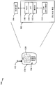
도 1 은 IC 디바이스들 사이에 통신 링크를 채용할 수도 있는 장치 (100) 를 도시한다. 일 예에 있어서, 장치 (100) 는 무선 액세스 네트워크 (RAN), 코어 액세스 네트워크, 인터넷 및/또는 다른 네트워크와 RF 트랜시버를 통해 통신하는 무선 통신 디바이스를 포함할 수도 있다. 장치 (100) 는 프로세싱 회로 (102) 에 동작가능하게 커플링된 통신 트랜시버 (106) 를 포함할 수도 있다. 프로세싱 회로 (102) 는 어플리케이션 특정 IC (ASIC) (108) 와 같은 하나 이상의 IC 디바이스들을 포함할 수도 있다. ASIC (108) 는 하나 이상의 프로세싱 디바이스들, 로직 회로들 등을 포함할 수도 있다. 프로세싱 회로 (102) 는, 프로세싱 회로 (102) 에 의해 실행될 수도 있는 명령들 및 데이터를 유지할 수도 있는 메모리 (112) 와 같은 프로세서 판독가능 저장부를 포함하고/하거나 그 프로세서 판독가능 저장부에 커플링될 수도 있다. 프로세싱 회로 (102) 는, 무선 디바이스의 메모리 디바이스 (112) 와 같은 저장 매체들에 상주하는 소프트웨어 모듈들의 실행을 지원 및 가능케 하는 어플리케이션 프로그래밍 인터페이스 (API) (110) 계층 및 오퍼레이팅 시스템 중 하나 이상에 의해 제어될 수도 있다. 메모리 디바이스 (112) 는 판독 전용 메모리 (ROM) 또는 랜덤 액세스 메모리 (RAM), 전기적으로 소거가능한 프로그래밍가능 ROM (EEPROM), 플래시 카드들, 또는 프로세싱 시스템들 및 컴퓨팅 플랫폼들에서 사용될 수 있는 임의의 메모리 디바이스를 포함할 수도 있다. 프로세싱 회로 (102) 는, 장치 (100) 를 구성 및 동작시키기 위해 사용된 동작 파라미터들 및 다른 정보를 유지할 수 있는 로컬 데이터베이스 (114) 를 포함하거나 로컬 데이터베이스 (114) 에 액세스할 수도 있다. 로컬 데이터베이스 (114) 는 데이터베이스 모듈, 플래시 메모리, 자기 매체들, EEPROM, 광학 매체들, 테이프, 소프트 또는 하드 디스크 등등 중 하나 이상을 사용하여 구현될 수도 있다. 프로세싱 회로 (102) 는 또한, 다른 컴포넌트들 중, 안테나 (122), 디스플레이 (124), 버튼 (128) 과 같은 오퍼레이터 제어부들, 및 키패드 (126) 와 같은 외부 디바이스들에 동작가능하게 커플링될 수도 있다.Figure 1 illustrates an
장치 (100) 는 서로 통신하는 복수의 프로세싱 회로들 (102), 트랜시버들 (106), 모뎀들 및 다른 디바이스들을 포함할 수도 있다. 각각의 프로세싱 회로 (102) 는 하나 이상의 ASIC들 (108), 프로세서들, 시퀀서들, 상태 머신들, 마이크로제어기들, 및 다른 로직 엘리먼트들을 포함한 복수의 IC 디바이스들로서 구현될 수도 있다. 다양한 상이한 엘리먼트들, 디바이스들, 회로들, 모듈들 및 기능부들이 장치 (100) 내에서 데이터 및 제어 정보를 전달하거나, 전송하거나, 라우팅하거나, 중계하거나 그렇지 않으면 통신하기 위해 서로 상호접속하도록 적응될 수도 있다. 일부 경우들에 있어서, 상이한 엘리먼트들, 디바이스들, 회로들, 모듈들 및 기능부들은 상이한 주파수들에서 클록킹되고/되거나 상이한 데이터 레이트들에서 통신 가능하다. 이에 따라, 엘리먼트들, 디바이스들, 회로들, 모듈들 및 기능부들을 상호접속시키는 데이터 통신 링크들은 통상적으로, 가변 수의 접속된 엘리먼트들, 디바이스들, 회로들, 모듈들 및 기능부들로의 액세스를 제공하도록 적응가능해야 한다.
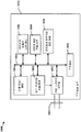
도 2 는 무선 통신 디바이스로서 동작할 수도 있는 장치 (200) 의 단순화된 예를 도시한 블록 다이어그램이다. 장치 (200) 는, 개별 다이스 상에서 형성될 수도 있고 및/또는 동일하거나 상이한 칩 캐리어들 상에서 또는 동일하거나 상이한 패키지들 내에서 제공될 수도 있는 복수의 IC 디바이스들 (202, 204, 206, 및 208) 을 포함한다. IC 디바이스들 (202, 204, 206, 및/또는 208) 중 2 이상은 통신 링크 (210) 를 통해 데이터 및 제어 정보를 교환할 수도 있다. 통신 링크 (210) 는, 서로 매우 근접하게 위치되거나 장치 (200) 의 상이한 부분들에서 물리적으로 위치된 IC 디바이스들 (202, 204, 206, 및/또는 208) 중 2 이상을 접속시키기 위해 사용될 수도 있다. 일 예에 있어서, 통신 링크 (210) 는, IC 디바이스들 (202, 204, 206, 및 208) 을 반송하는 칩 캐리어, 기판 또는 회로 보드 상에 제공될 수도 있다.2 is a block diagram illustrating a simplified example of an
IC 디바이스들 (202, 204, 206, 및 208) 은 동일한 IC 디바이스 (202, 204, 206, 또는 208) 의 다른 컴포넌트들과, 그리고 외부 데이터 링크 (210) 를 통해 다른 IC 디바이스들 (202, 204, 206, 및/또는 208) 의 컴포넌트들과 통신하도록 구성될 수도 있는 기능 컴포넌트들을 각각 포함할 수도 있다. 각각의 IC 디바이스 (202, 204, 206, 또는 208) 내의 컴포넌트들은 프로세싱 회로들 (226, 246, 266 및 282), 저장부 (286), 트랜시버들, 모뎀들, UART들, 디바이스 드라이버들 등등 (컴포넌트들 (222a, 222b, 222c, 242a, 242b 및 262) 로서 일반적으로 도시됨) 을 포함할 수도 있다. 일 예에 있어서, 일반 프로세싱 디바이스 (208) 는, 디지털 신호 프로세서 (DSP), 마이크로프로세서, 마이크로제어기, 시퀀서 로직, 상태 머신들 등과 같은 하나 이상의 프로세싱 회로들 (282) 을 포함하는 ASIC 으로서 제공되고 그리고 저장 디바이스 (286) 를 포함한 회로들을 지원할 수도 있다. 다른 예에 있어서, 일반 프로세싱 디바이스 (208) 는 동적 랜덤 액세스 메모리 (DRAM) 또는 다른 저장 디바이스들 (286) 을 사용하는 벌크 저장부 및 하나 이상의 프로세싱 회로들 (282) 을 제공하는 메모리 제어기 또는 메모리 서브시스템일 수도 있다. IC 디바이스들 (202, 204, 206 및 208) 의 내부 컴포넌트들은, 본 명세서에 개시된 특정 양태들에 따라 구성된 병렬 또는 직렬 버스 또는 통신 링크를 포함할 수도 있는 내부 데이터 링크들 (224, 244, 264 및 284) 을 사용하여 서로 통신할 수도 있다.The IC devices 202,204, 206 and 208 may be coupled to other components of the same IC device 202,204, 206 or 208 and to other IC devices 202,204 , 206, and / or 208), which may be configured to communicate with each other. The components in each
IC 디바이스들 (202, 204, 206, 및/또는 208) 중 하나 이상은 내부 데이터 링크들 (224, 244, 264 및/또는 284) 과 외부 데이터 링크 (210) 간의 인터페이스를 제공하기 위해 게이트웨이 회로 또는 컴포넌트 (220, 240, 260 및 280) 를 가질 수도 있다. 일부 경우들에 있어서, 게이트웨이 (220, 240, 260 또는 280) 는, 병렬-직렬 변환, 직렬-병렬 변환, 클록 레이트 차이들을 수용하기 위한 데이터 버퍼링, 로직 레벨 전환, 라인 드라이버들 등을 포함할 수도 있는 버스 전환 능력들을 제공할 수도 있다. 일부 예에 있어서, 게이트웨이 (220, 240, 260 또는 280) 는, 내부 데이터 링크들 (224, 244, 264 및/또는 284) 및 외부 데이터 링크 (210) 가 공통 아키텍처를 갖는 경우를 포함하여, 어드레스 전환 및/또는 어드레스 레졸루션을 제공할 수도 있다. 일 예에 있어서, 내부 데이터 링크들 (224, 244, 264 및/또는 284) 및 외부 데이터 링크 (210) 는 MP-CxMi 데이터 링크들을 포함할 수도 있다.One or more of the
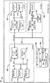
도 3 은 공존 관리를 위해 및/또는 한계 관리 (LM) 및 다른 기능들을 지원하기 위해 2개의 MP-CxMi 데이터 링크들 (310, 312) 을 채용하는 장치 (300) 의 일 예를 도시한 블록 다이어그램이다. 일 예에 있어서, 무선 통신 디바이스는 복수의 디바이스들, 회로들 (302, 304, 306 및 308) 및 그 특정 기능 컴포넌트들 (본 명세서에서 "CxMi 노드들" 로서 대체가능하게 지칭됨) 간의 통신을 지원하기 위한 제 1 MP-CxMi 데이터 링크 (310), 및 IC 디바이스들 (302, 304, 306 및 308) 에 의해 지원된 LM 기능들을 위해 전용되는 제 2 MP-CxMi 통신 링크 (312) 를 제공할 수도 있다. 일 예에 있어서, 전용 LM MP-CxMi 통신 링크 (312) 는 전용 게이트웨이 (318) 를 통해 제 1 IC 디바이스 (302) 의 대응하는 내부 LM MP-CxMi 통신 링크 (314a) 와 접속할 수도 있다. 내부 LM MP-CxMi 통신 링크 (314s) 는, 프라이머리 외부 MP-CxMi 통신 링크 (310) 로의 액세스를 제공하는 게이트웨이 (320) 를 통해 다른 CxMi 노드들에 접속할 수도 있다. 다른 CxMi 노드들은 글로벌 네비게이션 위성 시스템 (GNSS) 및 LM 접속들을 갖는 액세스 포인트 큐 (APQ) (302), GNSS 를 갖는 모뎀 (304), 듀얼 SIM 듀얼 활성 디바이스들을 위한 단일 칩 조합 디바이스 (306), 및 WLAN, 블루투스, FM 및 근접장 통신 (NFC) 모뎀들을 지원하는 결합 디바이스 (308) 의 하나 이상의 노드들을 포함할 수도 있다.3 is a block diagram illustrating an example of a
장치 (300) 의 다양한 엘리먼트들, 디바이스들, 회로들, 모듈들, 및 기능부들은 MP-CxMi 통신 링크 (310, 312, 314a-314d, 316a-316d) 를 사용하여 상호접속될 수도 있다. 하나의 외부 MP-CxMi 통신 링크 (310) 는 IC 디바이스들 (302, 304, 306 및 308) 을 상호접속시키는 한편, 내부 MP-CxMi 통신 링크들 (314a-314d 및 316a-316d) 은 외부 MP-CxMi 통신 링크 (310, 312) 를 연장하여, 각각, 대응하는 IC 디바이스들 (302, 304, 306 및 308) 내의 엘리먼트들, 디바이스들, 회로들, 모듈들 및 기능부들을 상호접속시킬 수도 있다.The various elements, devices, circuits, modules, and functions of the
CxMi 노드들의 결과적인 MP-CxMi 네트워크는 포인트-투-포인트 (P2P) 및 멀티캐스트 통신을 지원하도록 구성될 수도 있다. CxMi 노드들은 모뎀들 또는 다른 기능부들과 연관될 수도 있다. 각각의 IC 디바이스 (302, 304, 306 및 308) 는 하나 이상의 내부 CxMi 노드들을 지원할 수도 있고, CxMi 노드들의 수는 IC 디바이스 (302, 304, 306 및 308) 에 의해 핸들링된 기능들의 수에 기초할 수도 있다.The resulting MP-CxMi network of CxMi nodes may be configured to support point-to-point (P2P) and multicast communication. CxMi nodes may be associated with modems or other functionalities. Each
IC 디바이스들 (302, 304, 306 및 308) 은, 하나 이상의 CxMi 노드들의 동작들을 관리하도록 구성될 수 있는 프로세서 또는 다른 프로세싱 및/또는 컴퓨팅 회로 또는 디바이스를 각각 포함할 수도 있다. 일부 경우들에 있어서, 하나 이상의 CxMi 노드들은 시퀀서 또는 상태 머신에 의해 제어될 수도 있다.
MP-CxMi 통신 시스템은 완전 집적된 및 비-집적된 IC 디바이스들 (302, 304, 306 및 308) 과 함께 사용될 수도 있으며, 공통 호스트 제어기 인터페이스 (HCI) 가 장치 (300) 에 대해 정의될 수도 있다. 이에 따라, 상위 레벨 소프트웨어는 장치 (300) 를 제어하기 위해 사용될 수도 있다. 공통 인터페이스 소프트웨어는, 장치 (300) 내에 배치될 수도 있는 모뎀들/트랜시버들의 타입들의 조합에 무관하게 사용될 수도 있다. 예를 들어, 장치 (300) 는 GSM 및/또는 LTE 모뎀들을 포함할 수도 있으며, 뿐만 아니라, 무선 로컬 영역 네트워크 (WLAN) 트랜시버 (320b), 블루투스 트랜시버 (320a), 및 다른 엔드-포인트 모뎀들 또는 트랜시버들 (320c, 320d) 은 집적될 수도 있으며, MP-CxMi 통신 링크 (310, 312, 314a-314d 및/또는 316a-316d) 를 통해 공통 HCI 에 응답할 수도 있다.The MP-CxMi communication system may be used with fully integrated and
특정 예들에 있어서, 외부 MP-CxMi 통신 링크 (310 또는 312) 는 특별한 물리 계층 드라이버들 및 다른 디바이스들에 대한 요건없이 단순 CMOS 신호들을 사용하여 동작할 수도 있다. 외부 MP-CxMi 통신 링크 (310 또는 312) 는 50 Mbps (megabits per second) 이상의 데이터 레이트로 데이터를 반송하도록 구성될 수도 있다. MP-CxMi 통신 링크 (310 또는 312) 는 유연하게 설계될 수도 있으며, 데이터 레이트는 송신 CxMi 노드에 의해 결정될 수도 있다. 지연 및 연기 파라미터들은 또한 유연하게 구성될 수도 있으며, 일 예에 있어서, 구성 레지스터들에 의해 유지된 파라미터들에 의해 구성될 수도 있다.In certain instances, the external MP-
일 동작 모드에 있어서, 송신 CxMi 노드는 송신 클록을 소싱한다. 어떠한 미리정의된 버스 마스터도 채용되지 않으며, 송신 CxMi 노드는 메시지 송신의 지속기간 동안 버스를 제어 또는 마스터할 수도 있다. 경합 해결은 모든 메시지가 송신되기 전에 수행되고, 이에 의해, 메시지의 송신이 경합 해결에 참여할 시에, 오직 버스 상으로 송신하길 원하는 그 CxMi 노드들만이 경합 해결에 참여한다.In one operating mode, the transmitting CxMi node sourcing the transmit clock. No predefined bus masters are employed, and the transmitting CxMi node may control or master the bus for the duration of the message transmission. The contention resolution is performed before all messages are transmitted, so that when the transmission of a message participates in a contention resolution, only those CxMi nodes that want to transmit on the bus participate in contention resolution.
각각의 CxMi 노드는 고유의 어드레스를 갖고, 이 고유의 어드레스는 HCI 레지스터를 통해 프로그래밍되거나 구성될 수 있다. 각각의 CxMi 노드는 P2P 모드에서 하나의 다른 노드로 메시지를 지향시키거나 또는 포인트-투-멀티포인트 (P2MP) 모드에서 모든 노드들로 메시지를 멀티캐스팅할 수 있다. P2MP 송신들은 멀티캐스트 어드레스들을 사용하여 용이하게 될 수도 있으며, 다수의 상이한 멀티캐스트 어드레스들은 CxMi 노드들의 네트워크 내에서 서브넷들을 정의하기 위해 정의될 수 있다. 일 예에 있어서, 공존 엘리먼트들은 하나의 서브넷을 할당받고, 센서들은 다른 서브넷에 할당되며, 열 관리 엘리먼트들은 다른 서브넷에 할당되는 등일 수도 있다. 다양한 서브넷들은 외부 MP-CxMi 통신 링크 (310 또는 312) 의 동일한 2개의 와이어들을 통해, 그리고 각각의 IC 디바이스 (302, 304, 306 또는 308) 내에서, 대응하는 내부 MP-CxMi 통신 링크 (314a-314d 또는 316a-316d) 상으로 접속되거나 커플링될 수도 있다. 이에 따라, 모든 IC 디바이스들과 서브넷들 간의 통신은 IC 디바이스들 (302, 304, 306 및/또는 308) 사이의 동일한 2개의 와이어들을 사용하여 실시될 수도 있다.Each CxMi node has a unique address, which can be programmed or configured via the HCI register. Each CxMi node can direct messages from P2P mode to one other node or multicast messages to all nodes in point-to-multipoint (P2MP) mode. P2MP transmissions may be facilitated using multicast addresses, and a number of different multicast addresses may be defined to define subnets within the network of CxMi nodes. In one example, coexistence elements may be assigned one subnet, sensors may be assigned to different subnets, thermal management elements may be assigned to different subnets, and so on. The various subnets may be routed through the same two wires of the external MP-
각각의 IC 디바이스 (302, 304, 306 또는 308) 는 프로세서 또는 다른 프로세싱 및/또는 컴퓨팅 회로 또는 디바이스, 및 IC 디바이스들 (302, 304, 306 및/또는 308) 상의 개별 프로세서들 및/또는 IC 디바이스들 (302, 304 및 306) 의 다른 컴포넌트들에 의해 사용된 명령들 및 데이터를 유지하도록 적응될 수도 있는 일시적인 및/또는 비-일시적인 저장 디바이스들을 포함한 저장 매체들을 가질 수도 있다.Each
도 4 는 복수의 IC 디바이스들 (402, 404 및 406) 을 접속시키기 위해 그리고 IC 디바이스들 (402, 404, 406) 내의 기능 엘리먼트들 또는 컴포넌트들 (420, 422a, 442b, 422c, 440, 442a, 442b, 460 및 462) 을 접속시키기 위해 MP-CxMi 를 채용하는 단순화된 장치 (400) 를 도시한 블록 다이어그램이다. 도시된 IC 디바이스들 (402, 404, 406) 각각은, 기능 엘리먼트들 또는 컴포넌트들 (420, 422a, 442b, 422c, 440, 442a, 442b, 460 및 462) 로 하여금 내부 MP-CxMi 데이터 링크들 (426, 446, 466) 을 통해 그리고 외부 MP-CxMi 데이터 링크 (410) 를 통해 상호접속 및 통신할 수 있게 하는 다양한 전환 서비스들을 제공하는 게이트웨이 (420, 440, 460) 를 포함한다. 게이트웨이들 (420, 440, 460) 은 레벨 전환, 버퍼링 및 클록 레이트 변환 서비스들을 제공할 수도 있다. 각각의 MP-CxMi 데이터 링크 (410, 426, 446, 466) 는 통상적으로, 데이터 및 클록 신호들 양자를 반송한다. 각각의 내부 컴포넌트 (422a, 422b, 422c, 442a, 442b 및 462) 는, 각각, 인터페이스 (CxMi 노드) (424a, 424b, 424c, 444a, 444b 및 464) 를 통해 개별 내부 CxMi 데이터 링크들 (426, 446 및 466) 에 접속될 수도 있다.Figure 4 illustrates a method for connecting a plurality of IC devices 402,404 and 406 and for connecting functional elements or
게이트웨이들 (420, 440 및/또는 460) 및 노드들 (424a, 424b, 424c, 444a, 444b 및/또는 464) 은 하나 이상의 상태 머신들 또는 다른 제어기들 또는 시퀀서들에 의해 제어될 수도 있다. 상태 머신들은 단순 실시간 이벤트들을 낮은 레이턴시로 효율적으로 전송할 수 있다. 상태 머신들은 노드 연관식 모뎀에 또는 메시지를 전송하기 위해 구성된 통신 프로세서에 통신가능하게 커플링될 수도 있다.
이제, 장치 (400) 의 특정 동작 양태들이 도 5 내지 도 8 과 관련하여 설명된다.Specific operational aspects of the
도 5 는 MP-CxMi 통신 링크들 (410, 426, 446 및/또는 466) 상에서 사용될 수도 있는 메시지 (500) 의 특정 엘리먼트들을 도시한다. 메시지들은, MP-CxMi 프로토콜에 의해 효과적으로 터널링될 수도 있는 무선 공존 인터페이스 (WCI-2) 메시지들 (512) 을 포함할 수도 있다. WCI-2 메시지 (512) 는 멀티포인트 MP-CxMi 네트워크 (410, 426, 446 및/또는 466) 를 통해 송신될 수도 있으며, 메시지들은 특정 노드들 (424a, 424b, 424c, 444a, 444b 및 464) 에 또는 서브넷 상의 노드들의 그룹에 어드레싱될 수도 있다. 메시지는 소형 헤더를 뒤따라 255 바이트들까지 포함할 수 있다. MP-CxMi 메시지 (500) 에서 터널링되는 메시지 데이터의 상위 레벨 프로토콜을 식별하기 위해 사용될 수도 있는 메시지 타입 필드 (504) 가 헤더에 포함된다. 일 예에 있어서, 프로토콜은, 각각이 상이한 메시지 타입 값과 연관되는 표준화된 및 독점적인 데이터 타입들을 포함한 32개까지의 상이한 메시지 타입들을 지원할 수 있다.Figure 5 illustrates certain elements of a
다중의 노드들이 메시지들을 동시에 전송하려고 시도할 경우에 상위 우선순위 실시간 메시지들이 첫번째로 전송될 수 있게 하는 메시지 우선순위가 정의될 수도 있다. 메시지 우선순위 필드 (502) 는, 매 메시지 (500) 마다 전송되는 3비트 우선순위 값을 포함할 수도 있다. 일 예에 있어서, "0" 우선순위 값이 가장 높은 이용가능한 우선순위 및/또는 가장 긴급한 우선순위와 연관되는 한편 "7" 의 우선순위 값이 가장 낮은 그리고 가장 적게 긴급한 우선순위이도록, 하위 우선순위 값들은 상위 우선순위들에 대응한다. 시스템 설계자는, 실시간 이벤트들에 대응하는 메시지들의 효율적인 전달을 보장하기 위하여 각각의 메시지 타입에 대한 적절한 우선순위들을 선택할 수도 있다. 예를 들어, 타입-0 WCI-2 메시지들 (512) 에는 가장 높은 우선순위가 할당될 수도 있고, 타입-2 WCI-2 메시지들 (512) 에는 가장 낮은 우선순위가 할당될 수도 있다. 시스템 설계자는 3비트 우선순위 필드 (502) 에 의해 제공된 8개 미만의 이용가능한 우선순위 레벨들을 사용할 수도 있고/있거나 외부 MP-CxMi 버스 (410) 상의 중재 페이즈 (phase) 의 오버헤드를 감소하기 위해 우선순위 레벨들의 작은 서브세트를 활용할 수도 있다.A message priority may be defined that allows higher priority real time messages to be sent first when multiple nodes attempt to simultaneously transmit messages. The
각 메시지 타입의 우선순위는 다양한 방식들로 설정될 수 있다. 설명의 단순화를 위해, 노드는 전송될 메시지 데이터를 수신함과 병렬로 노드 인터페이스 회로들의 디바이스측으로부터 3비트 우선순위 필드 (502) 를 수신한다고 가정될 것이다.The priority of each message type may be set in various manners. For simplicity of the description, it will be assumed that the node receives the 3-
본 명세서에서 개시된 특정 양태들에 따르면, 다중의 디바이스들 (402, 404 및 406) 이 MP-CxMi 버스 (410) 에 접속될 경우, 외부 MP-CxMi 버스 (410) 로의 액세스를 중재하기 위해 최단 펄스 폭 방법이 사용될 수도 있다. 동시에 송신하길 원하는 복수의 디바이스들 (402, 404 및/또는 406) 에 대한 우선순위는, 상위 우선순위 메시지들이 최단 어써트 펄스에 의해 식별될 경우에 리졸브(resolve)될 수도 있다. 상위 우선순위 메시지들에 대해 더 짧은 펄스들을 사용하는 것은 고 우선순위 메시지들에 대한 오버헤드를 감소시킬 수 있다. 일부 경우들에 있어서, 메시지 우선순위 필드 (502) 의 실제 디지털 콘텐츠는 외부 MP-CxMi 버스 (410) 가 아닌 오직 내부 MP-CxMi 버스 (426, 446 및/또는 466) 상으로 송신된다. 메시지가 외부 버스 (410) 상으로 송신되려 하면, 메시지 우선순위 (502) 는 중재 페이즈에서 어써트 펄스 폭으로 변환될 수도 있는데, 왜냐하면 이 필드는 메시지 (500) 가 외부 버스를 통해 수신 게이트웨이들 (420, 440 및/또는 460) 로 전달된 이후에 더 이상 필요하지 않기 때문이다.According to certain aspects disclosed herein, when
일 예에 있어서, "3" 으로 설정된 어드레스를 갖는 제 1 CxMi 노드 (424a, 424b, 424c, 444a, 444b 또는 464) 는 "5" 로 설정된 어드레스를 갖는 제 2 CxMi 노드 (424a, 424b, 424c, 444a, 444b 또는 464) 로 P2P 메시지를 송신할 수도 있다. 메시지 목적지 어드레스 필드 (506) 는 "5" 로 설정될 수도 있고, 소스 어드레스 필드 (508) 는 "3" 으로 설정될 수도 있다. CxMi 노드 (424a, 424b, 424c, 444a, 444b 또는 464) 가 메시지 (500) 를 전송할 경우, 모든 수신 노드들 (424a, 424b, 424c, 444a, 444b 및/또는 464) 이 메시지 (500) 를 볼 수 있도록 게이트웨이 (420, 440 및/또는 460), 외부 MP-CxMi 버스 (410) 및 대응하는 내부 MP-CxMi 버스들 (426, 446 및/또는 466) 을 통해 라우팅된다.In one example, a
본 명세서에서 개시된 하나 이상의 양태들에 따른 펄스 폭 기반 경합 해결 방식은 외부 MP-CxMi 버스 (410) 에 대한 우선순위를 리졸브할 수 있다. 외부 MP-CxMi 버스 (410) 의 제어를 위해 경합하는 각각의 노드 (즉, 게이트웨이들 (420, 440 및/또는 460)) 는 "레벨 설정 및 모니터" 절차를 수행하여, 상위 우선순위 노드 (420, 440 또는 460) 가 버스 (410) 의 제어를 취하였는지 여부를 결정한다. MP-CxMi 신호들을 외부 MP-CxMi 버스 (410) 에 커플링하기 위한 I/O 패드 회로는 고 임피던스 능력을 갖는 표준 CMOS I/O 패드 회로를 포함할 수도 있다. 킵퍼 회로 (도 8 참조) 는, 경합 노드들 (420, 440 및/또는 460) 을 포함한 모든 데이터 드라이버 회로들이 고 임피던스 상태에 있을 경우에 버스 (410) 의 상태를 데이터 하이 상태로 또는 데이터 로우 상태로 유지하도록 구성될 수도 있다. 외부 MP-CxMi 버스 (410) 의 클록 신호는, 경합 프로세스 동안을 포함하여 어떠한 디바이스도 클록을 구동하고 있지 않을 경우 클록을 로우 상태로 유지하는 풀-다운 전류 소스로 구성될 수도 있다.A pulse width based contention resolution scheme in accordance with one or more aspects disclosed herein may resolve priorities for an external MP-
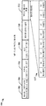
도 6 은 도 5 에 도시된 메시지 (500) 와 같은 MP-CxMi 메시지의 송신을 도시한 타이밍 다이어그램 (600) 이다. 메시지 (500) 는 데이터 페이즈 (608) 동안 MP-CxMi 통신 링크들 (410, 426, 446 및/또는 466) 중 하나 이상의 MP-CxMi 통신 링크들 상으로 송신될 수도 있다. 메시지 (500) 는 송신기에 의해 제공된 클록 (604) 을 사용하여 커넥터들의 쌍 상으로 데이터 (602) 로서 송신될 수도 있다. 데이터 페이즈 (608) 에서 메시지 (500) 를 송신하기 위하여, 송신기는 중재 페이즈 (606) 동안 필요한 MP-CxMi 통신 링크들 (410, 426, 446 및/또는 466) 의 제어를 획득하려고 시도한다. 본 명세서에서 개시된 특정 양태들에 따르면, MP-CxMi 통신 링크 (410) 의 제어는 신호들의 타이밍에 기초한 프로토콜을 사용하여 중재 페이즈 (606) 동안 획득된다.FIG. 6 is a timing diagram 600 illustrating the transmission of an MP-CxMi message, such as the
중재 페이즈 (602) 는, 가장 높은 우선순위 메시지가 첫번째로 송신됨을 보장하는 중재 프로세스를 사용하여 필요한 MP-CxMi 통신 링크들 (410, 426, 446 및/또는 466) 의 제어를 위해 경합하는 복수의 CxMi 노드들 (424a, 424b, 424c, 444a, 444b 및/또는 464) 에 의해 MP-CxMi 통신 버스 (410) 상으로 전송될 메시지들 (500) 에 대한 메시지 우선순위를 리졸브할 수 있다. 우선순위는 메시지 (500) 의 메시지 우선순위 필드 (502) 의 콘텐츠 또는 값과 송신 게이트웨이 (420, 440 또는 460) 에 할당된 게이트웨이 어드레스의 조합으로부터 생성된 타이밍에 기초하여 리졸브될 수도 있다. 일 예에 있어서, 수치 게이트웨이 어드레스 및 메시지 우선순위 변수들에 적용된 상대적으로 단순한 알고리즘은, 메시지 (500) 의 우선순위를 결정하는 계산된 우선순위 값을 생성할 수도 있다.The arbitration phase 602 includes a plurality of contending competing messages for control of the required MP-
가장 높게 계산된 우선순위 값은 어느 경합 CxMi 노드 (424a, 424b, 424c, 444a, 444b 또는 464) 가 MP-CxMi 통신 링크들 (410, 426, 446 및/또는 466) 에 대한 경합에서 승리할 지를 결정할 수도 있다. MP-CxMi 통신 링크들 (410, 426, 446 및/또는 466) 에 대한 경합에서 승리한 CxMi 노드 (424a, 424b, 424c, 444a, 444b 또는 464) 는 내부 MP-CxMi 통신 링크들 (426, 446 및/또는 466) 중 하나 이상 및/또는 외부 MP-CxMi 통신 링크 (410) 로의 액세스를 제어할 수 있다. 노드 소스 어드레스 (508) 는, 2 이상의 메시지들이 동일한 계산된 우선순위 값을 가질 경우에 타이(tie)를 깨는데 사용될 수도 있다.The highest calculated priority value indicates whether any
CxMi 메시지들 (500) 은 데이터 페이즈 (608) 동안 송신될 수도 있다. 도 5 에 도시된 예에 있어서, CxMi 메시지 (500) 의 필드들은, 외부 MP-CxMi 통신 링크 (410) 상의 데이터 압축을 위해 CxMi 게이트웨이 (420, 440 또는 460) 에 의해 합성될 수도 있는 매우 짧은 헤더 (VSH) 필드 (622) 를 포함한다. VSH 필드 (622) 는 통상적으로 첫번째로 송신된다. 일 예에 있어서, VSH 필드 (622) 가 0 내지 6 의 값을 가지면, 메시지 타입 필드 (504), 목적지 노드 어드레스 필드 (506), 소스 노드 어드레스 필드 (508), 및 메시지 데이터 길이 필드 (510) 는 송신될 필요가 없는데, 왜냐하면 이들 필드들은 HCI 내의 레지스터들의 7개 세트들 중 하나로부터 획득될 수 있기 때문이다. 하지만, VSH 필드 (622) 가 7 의 값을 가지면, 메시지 타입 필드 (504) 는, 목적지 노드 어드레스 필드 (506), 소스 노드 어드레스 필드 (508), 및 메시지 데이터 길이 필드 (510) 를 포함한 필드들 (626) 이 뒤따르는 데이터 페이즈 (608) 의 다음 필드 (624) 에서 송신된다. 메시지 타입 필드 (504), 목적지 노드 어드레스 필드 (506), 소스 노드 어드레스 필드 (508), 및 메시지 데이터 길이 필드 (510) 에 대한 메시지 헤더 필드들의 길이들은 통상적으로 HCI 내의 레지스터들에 의해 명시된다.
송신된 VSH 필드 (622) 가 7 의 값을 가질 경우, 옵션적인 필드들 (626) 은 메시지 타입 필드 (504), 목적지 노드 어드레스 필드 (506), 소스 노드 어드레스 필드 (508), 및 메시지 데이터 길이 필드 (510) 를 포함한다.
메시지 타입 필드 (504) 는, MP-CxMi 인터페이스를 통해 터널링되는 프로토콜 또는 메시지의 타입을 식별한다.The
목적지 노드 어드레스 필드 (506) 는, 메시지의 의도된 수신자인 CxMi 노드 (424a, 424b, 424c, 444a, 444b 및/또는 464) 의 노드 어드레스를 명시한다. 어드레스는 또한, 다중의 CxMi 노드들 (424a, 424b, 424c, 444a, 444b 및/또는 464) 로 하여금 메시지 (500) 를 수신하게 하는 멀티캐스트 어드레스일 수도 있다.The destination
소스 노드 어드레스 필드 (508) 는, 메시지가 발신된 CxMi 노드 (424a, 424b, 424c, 444a, 444b 또는 464) 의 노드 어드레스를 포함한다.The source node address field 508 contains the node address of the
메시지 데이터 길이 필드 (510) 는, 뒤이어지는 메시지 데이터 (628) 의 바이트들의 수를 포함한다. 메시지 데이터는 메시지 (500) 의 페이로드를 포함한다.The message
메시지들 (500) 은, 경합 CxMi 노드 (424a, 424b, 424c, 444a, 444b 또는 464) 가 MP-CxMi 메시지 (500) 의 각각의 송신에 선행하는 버스 중재 프로세스에 승리함으로써 외부 MP-CxMi 버스 (410) 의 제어를 획득한 이후에 외부 MP-CxMi 버스 (410) 상으로 전송된다. 송신될 메시지 (500) 를 갖는 각각의 CxMi 게이트웨이 (420, 440 및/또는 460) 가 버스 중재에 참여할 수도 있다. 전송할 어떠한 CxMi 메시지 (500) 도 갖지 않는 임의의 CxMi 게이트웨이 (420, 440 및/또는 460) 는 버스 활동을 무시하고 슬립 모드로 진입하거나 남겨질 수도 있다. CxMi 게이트웨이 (420, 440 및/또는 460) 는 버스 활동을 모니터링하여, 현재 CxMi 메시지 (500) 의 송신이 완료할 때를, 특히, 모니터링 CxMi 노드 (424a, 424b, 424c, 444a, 444b 또는 464) 가 전송할 메시지 (500) 를 갖거나 수신할 때를 결정할 수도 있다.
중재 프로세스에서 승리하지 않은 경합 CxMi 노드 (424a, 424b, 424c, 444a, 444b 및/또는 464) 는 슬립 모드에 진입할 수도 있다. 슬립 모드에 있어서, CxMi 노드 (424a, 424b, 424c, 444a, 444b 및/또는 464) 는 메시지들을 수신할 수 있다. 수신기는, 로직이 오직 CxMi 인터페이스 클록에 의해서만 클록킹될 경우라도 (예를 들어, 내부 클록이 전력을 보존하기 위해 디스에이블링됨), 로직이 파워-온될 경우 메시지가 수신기로 어드레싱되는지 여부를 결정할 수 있다. 일부 경우들에 있어서, CxMi 노드 (424a, 424b, 424c, 444a, 444b 및/또는 464) 는 임의의 메시지의 수신 시 슬립 모드를 퇴장하도록 구성될 수도 있다. 일부 경우들에 있어서, CxMi 노드 (424a, 424b, 424c, 444a, 444b 및/또는 464) 는 특정한 미리결정된 웨이크업 메시지들의 수신 시 슬립 모드를 퇴장하도록 구성될 수도 있다. CxMi 노드 (424a, 424b, 424c, 444a, 444b 및/또는 464) 로 하여금 슬립 모드를 퇴장하게 하는 메시지는, CxMi 노드 (424a, 424b, 424c, 444a, 444b 및/또는 464) 가 웨이크 업 이후 평가할 수 있는 부가적인 데이터를 반송할 수도 있다.Contested
도 7 은 3개의 CxMi 게이트웨이들 (420, 440 및 460) 사이의 버스 중재 프로세스 (700) 의 일 예를 도시한 타이밍 다이어그램이다. 중재 프로세스 (700) 는, 데이터 신호 (702) 및/또는 클록 신호 (704) 가 통상적으로 중재 클록 사이클들의 배수로서 측정되는 미리정의된 시간 동안 유휴상태로 남겨진 이후에 개시될 수도 있다. 도시된 예 (700) 에 있어서, 유휴 상태는 로직 로우 레벨로서 정의될 수도 있다. 중재 클록 사이클에 기반한 시간의 유닛은 송신 유닛 (TU) 로서 지칭될 수도 있다. TU 는 통상적으로, 상이한 클록 속도들에서 동작할 수도 있는 IC 디바이스들 (402, 404 및 406) (도 4 참조) 과 같은 접속된 디바이스들의 가장 느린 클록 레이트를 수용하도록 선택된다. 통상적으로, TU 는 접속된 디바이스들의 가장 느린 클록 레이트의 정수배이고, 이러한 중재 클록 타이밍은 경합 CxMi 게이트웨이들 (420, 440 및 460) 에 의해 송신된 펄스 폭들이 중재 동안 일치된 길이들일 수 있게 한다.FIG. 7 is a timing diagram illustrating an example of a
데이터 신호 (702) 및 클록 신호 (704) 가 중재 프로세스 (700) 이전에 로우상태로 (또는 다른 유휴 상태로) 남겨지는 시간 주기는 가변일 수 있다. 일 예에 있어서, 복수의 경합 CxMi 게이트웨이들 (420, 440 및/또는 460) 은, 상이한 시간 주기들 동안 데이터 신호 (702) 및 클록 신호 (704) 에 대해 유휴 상태를 관측한 이후 중재 프로세스 (700) 를 개시하도록 구성될 수도 있다. CxMi 게이트웨이들 (420, 440 및/또는 460) 에는 상이한 우선순위들이 할당될 수도 있으며, 상위 우선순위 CxMi 게이트웨이들 (420, 440 및/또는 460) 은 하위 우선순위 CxMi 게이트웨이들 (420, 440 및/또는 460) 전에 중재 프로세스 (700) 를 개시하고, 이에 의해, 하위 우선순위 CxMi 게이트웨이들 (420, 440 및/또는 460) 을 선점할 수도 있다. 다른 예에 있어서, CxMi 게이트웨이들 (420, 440 및/또는 460) 은, 송신될 메시지 (500) 의 우선순위에 기초하여 결정된 시간 주기 동안 데이터 신호 (702) 및 클록 신호 (704) 에 대해 유휴 상태를 관측한 이후 중재 프로세스 (700) 를 개시하도록 구성될 수도 있다. 이러한 방식으로, 하위 우선순위를 갖는 메시지 (500) 는 상위 우선순위를 갖는 메시지 (500) 보다 더 긴 모니터 주기를 가질 수 있다.The time period in which the data signal 702 and the
도 7 에 도시된 예에 있어서, 경합 CxMi 게이트웨이들 (420, 440 및 460) 각각은 중재 프로세스 (700) 에 참여한다. CxMi 게이트웨이들 (420, 440 및 460) 은, 데이터 신호 (702) 및 클록 신호 (704) 가 2 이상의 TU들 동안 유휴상태로 남겨졌음을 결정한 이후 경합 중재에 진입할 수도 있다. 중재는, 경합 CxMi 게이트웨이들 (420, 440 및 460) 중 적어도 하나가 MP-CxMi 통신 링크 (410) 의 제어를 위해 경합하기 위해 데이터 신호 (702) 를 하이(high)로 구동할 경우에 시작한다. 경합 CxMi 게이트웨이들 (420, 440 및 460) 중 일부 또는 그 모두는 MP-CxMi 통신 링크 (410) 의 제어를 위한 그 개별 경합을 어써트하기 위해 데이터 신호 (702) 를 하이로 동시에 및/또는 일제히 구동할 수도 있다. 그 후, 각각의 참여하는 CxMi 게이트웨이 (402, 404 및 406) 는, 데이터 신호 (702) 를 로우(low)로 구동하기 전에 그 대응하는 메시지 (500) 에 대한 우선순위 값을 계산함으로써 결정된 시간 주기 동안 대기한다. 데이터 신호 (702) 가 그 시간 주기 이후 이미 로우이면, 대응하는 CxMi 게이트웨이 (420, 440 및/또는 460) 는 MP-CxMi 통신 링크 (410) 의 제어를 CxMi 메시지 (500) 의 상위 우선순위 송신기에 양보한다.In the example shown in FIG. 7, each of the
CxMi 게이트웨이 (402, 404 및 406) 가 데이터 신호 (702) 를 로우로 구동하기 전에 대기하는 시간 주기는 중재 펄스 (710, 718 또는 720) 의 폭을 계산하기 위한 알고리즘을 사용하여 결정될 수도 있다. 도시된 예 (700) 에 있어서, 그 알고리즘은 중재 펄스 (710, 718 또는 720) 의 지속기간 (t) 를 다음과 같이 계산한다:The time period in which the
t = TU * ((Message_Priority * NGateways) + (Gateway_Address + 1)),t = TU * ((Message_Priority * N Gateways ) + (Gateway_Address + 1)),
여기서, NGateways 는 MP-CxMi 통신 링크 (410) 에 접속된 CxMi 게이트웨이들 (420, 440 및 460) 의 수이다. 이 알고리즘에서의 가중화는 게이트웨이 어드레스에 대한 메시지 우선순위를 강조한다. 하지만, 게이트웨이 어드레스는, 동일한 메시지 우선순위를 갖는 메시지들 (500) 간의 타이브레이커 (tiebreaker) 로서 기능할 수 있다. 예를 들어, 상이한 CxMi 게이트웨이들 (420, 440 및/또는 460) 로부터의 2개의 메시지들 (500) 이 동일한 메시지 우선순위를 가질 경우, 가장 낮은 게이트웨이 어드레스를 갖는 CxMi 게이트웨이 (420, 440 또는 460) 로부터 전송된 메시지 (500) 는 중재 펄스들 (710, 718 또는 720) 의 최단치를 생성하기 때문에 중재 프로세스 (700) 에서 우세할 수도 있다.Where N Gateways is the number of
도시된 중재 프로세스 (700) 는, 송신될 메시지들을 갖는 3개의 CxMi 게이트웨이들 (420, 440 및 460) (NGateways=3) 사이의 중재의 일 예와 관련되며, 여기서:The illustrated
![]()
![]()
![]()
![]()
![]()
![]()
도시된 중재 프로세스 (700) 는, 데이터 신호 (702) 및 클록 신호 (704) 가 미리결정된 시간 주기 동안 로우로 풀링된 이후에 시작한다. 이 "유휴" 주기 동안, 모든 CxMi 게이트웨이들 (420, 440 및 460) 은 통상적으로 고 임피던스 상태에 있으며 어떠한 버스 마스터도 정의되지 않는다. 데이터 신호 (702) 및 클록 신호 (704) 는, 모든 CxMi 게이트웨이들 (420, 440 및 460) 이 고 임피던스 상태에 진입할 경우에 개별 킵퍼 회로들 (800) (도 8 참조) 에 의해 유지될 수도 있다. 일 예에 있어서, 3개의 CxMi 게이트웨이들 (420, 440 및 460) 은 고 임피던스 상태로 남겨지고 적어도 2 TU 동안 유휴 상태 (예를 들어, 로우 레벨) 에서 데이터 신호를 관측하도록 구성될 수도 있다. 다른 예에 있어서, 3개의 CxMi 게이트웨이들 (420, 440 및 460) 은 고 임피던스 상태로 남겨지고 상이한 또는 가변 시간 주기들 동안 유휴 상태 (예를 들어, 로우 레벨) 에서 데이터 신호를 관측하도록 구성될 수도 있다. CxMi 게이트웨이들 (420, 440 및 460) 은 MP-CxMi 통신 링크 (410) 의 제어를 위해 경합하기 위해 데이터 신호 (702) 를 하이로 동시에 및/또는 일제히 구동할 수도 있다. 제 1 CxMi 게이트웨이 (420) 는 1 TU 주기가 경과한 이후에 데이터 신호 (702) 를 로우로 풀링한다. 제 2 및 제 3 CxMi 게이트웨이들 (440 및 460) 은, 데이터 신호 (702) 가 로우로 구동되었음을 검출하고 그리고 다음 중재 페이즈 (706) 의 시작까지 고 임피던스 상태로 남겨진다. 제 2 및 제 3 CxMi 게이트웨이들 (440 및 460) 의 데이터 파형들 (714 및 716) 상의 점선들은, 어떠한 상위 우선순위 메시지도 송신을 위해 이용가능한 것으로 결정되지 않으면 발생되었던 펄스들 (718 및 720) 의 형태를 나타낸다. 제 1 CxMi 게이트웨이 (402) 는 통상적으로, 1 TU 이상의 지연 이후에 발생할 수도 있는, 버스 획득을 완료하였을 때까지 클록 신호를 구동하지 않는다.The illustrated
본 명세서에서 개시된 특정 양태들에 따르면, 중재 어써트 펄스 (710) 는 CxMi 게이트웨이들 (420, 440 및/또는 460) 중 하나 이상에 의해 개시되고, 최단의 계산된 중재 어써트 펄스 (710, 718 또는 720) 를 갖는 CxMi 게이트웨이 (420, 440 또는 460) 에 의해 종료된다. 도 7 에 도시된 예에 있어서, 제 1 CxMi 게이트웨이 (420) 는, 최단 중재 어써트 펄스 (710') 를 갖는 파형 (702') 를 생성하고, 데이터 페이즈 (708) 에 진입하기 전에 1 TU (712) 동안 데이터 신호 (702) 를 로우로 구동하는 것을 계속한다. 그 후, 제 1 CxMi 게이트웨이 (420) 는 CxMi 메시지 (500) 의 VSH 필드를 전송한다. 각각의 중재 프로세스 (700) 에 있어서, 중재 페이즈 (706) 의 총 경과 시간은 가변이고, 그 길이는, 중재 프로세스에서 우세한 메시지 (500) 과 연관된 게이트웨이 어드레스 및 메시지 우선순위에 의해 관리된다.According to certain aspects disclosed herein, the arbitration assert
제 2 및 제 3 CxMi 게이트웨이들 (440 및 460) 은, 제 1 CxMi 게이트웨이 (420) 가 상위 우선순위 메시지를 전송하길 원함과 동시에 하위 우선순위 메시지를 전송하기 위해 경합하고 있을 수도 있다. 제 2 CxMi 게이트웨이 (440) 는 펄스 (718) 를 개시할 수도 있고, 제 3 CxMi 게이트웨이 (460) 는 외부 MP-CxMi 통신 링크 (410) 상의 펄스 (720) 를 개시할 수도 있다. 그 후, 제 2 및 제 3 CxMi 게이트웨이들 (440 및 460) 은, 그 개별 펄스 (718 또는 720) 의 시간 주기가 만료할 때까지 데이터 신호 (702) 를 관측할 수도 있다. 하지만, 그 예에 있어서, 데이터 신호 (702) 는 상위 우선순위 제 1 CxMi 게이트웨이 (420) 에 의해 첫번째로 로우로 구동되어, 제 2 CxMi 게이트웨이 (440) 및 제 3 CxMi 게이트웨이 (460) 에게서 데이터 신호 (702) 를 하이 레벨로부터 로우 레벨로 스위칭할 기회를 빼앗고 그리고 제 2 CxMi 게이트웨이 (440) 가 버스 (410) 의 제어를 획득하는 것을 배제한다. 제 1 CxMi 게이트웨이 (420) 가 하위 우선순위 제 2 CxMi 게이트웨이 (440) 및 제 3 CxMi 게이트웨이 (460) 가 데이터 신호 (720) 를 로우로 구동하려고 시도하였을 시간 전에 데이터 신호 (702) 를 로우로 구동하였음을 관측하였으면, 제 2 CxMi 게이트웨이 (440) 및 제 3 CxMi 게이트웨이 (460) 는 고 임피던스 상태로 남겨지고 제 1 CxMi 게이트웨이 (720) 에 의한 송신을 모니터링하고, 후속하여, 다음 경합 프로세스가 시작할 수 있을 때를 결정하기 위해 데이터 신호 (702) 및 클록 신호 (704) 의 유휴 상태들을 모니터링한다.The second and
각각의 CxMi 게이트웨이 (420, 440 및 460) 에 대해, 일 TU 의 지속기간은 내부 클록을 분할하기 위해 구성 또는 프로그래밍된 클록 분할기를 사용하여 결정될 수도 있다. 내부 클록 및 클록 분할기는 게이트웨이 HCI 내의 게이트웨이 구성 레지스터를 통해 구성될 수도 있다. TU 는 통상적으로, 장치 (400) 에서의 모든 CxMi 게이트웨이들 (420, 440 및/또는 460) 의 가장 느린 이용가능한 클록에 의해 생성될 수 있는 지속기간을 갖도록 선택된다. 분수 분할기는, 합성된 클록의 피크-투-피크 변동이 충분한 정확도의 주기를 생성하면 그리고 다른 CxMi 게이트웨이들 (420, 440 및/또는 460) 로부터의 펄스들을 검출하기 위한 샘플링 윈도우가 충분히 정확하면, 사용될 수도 있다.For each
본 명세서에서 개시된 특정 양태들에 따르면, 경합 CxMi 게이트웨이들 (420, 440 및/또는 460) 은 데이터 신호 (702) 를 하이로 구동하고 0.5 TU 내에 고 임피던스 상태에 진입한다. 미구동된 데이터 신호 (702) 및/또는 미구동된 클록 신호 (704) 의 상태를 유지하기 위하여, 하나 이상의 킵퍼 회로들 (800) (도 8) 이 제공될 수도 있다. 킵퍼 회로 (800) 는 IC 디바이스 (402, 404, 406) 상에 내부적으로 배치되거나, 또는 모든 CxMi 게이트웨이들 (420, 440 및 460) 이 고 임피던스 모드에 진입하였을 경우에 데이터 신호 조건을 유지하기 위해 외부적으로 배치될 수도 있다. 중재 동안, 킵퍼 회로 (800) 는, 최고 우선순위 이벤트를 서빙하는 CxMi 게이트웨이 (420, 440 또는 460) 가 신호 라인 (812) 를 로우로 구동하고 따라서 최단 펄스를 생성할 때까지 신호 라인 (812) 를 하이로 유지한다. 도시된 예에 있어서, 킵퍼 회로 (800) 는, 데이터 신호를 그 최종 구동 상태로 유지하는 고 임피던스 피드백 저항기 (804) 를 갖는 비반전 게이트 (802) 를 포함할 수도 있다. 저항기 (804) 는, 무시할 수 있는 부하를 신호 라인 (812) 에 부가하고 활성 CxMi 게이트웨이 출력에 의해 용이하게 극복되는 충분히 높은 저항을 갖는다.According to certain aspects disclosed herein, the
최단 펄스의 주기의 말단에서, 최단 펄스와 연관된 CxMi 게이트웨이 (420, 440 또는 460) 는 고 임피던스 상태를 퇴장하고 신호 라인 (812) 을 구동한다. 예를 들어, 중재 프로세스 (700) 에서 승리한 CxMi 게이트웨이 (420, 440 또는 460) 는 0.5 TU 동안 데이터 신호 (702) 를 로우로 구동하고, 중재 페이즈 (706) 의 종료 이후 클록 신호 (704) 를 구동한다. 전송하기 위한 하위 우선순위 메시지들을 갖는 경합 CxMi 게이트웨이들 (420, 440 및/또는 460) 은 데이터 신호 (704) 가 로우로 구동되었음을 검출하고 중재 프로세스 (700) 를 퇴장할 수도 있다. 중재 프로세스 (700) 에서 우세하지 않은 CxMi 게이트웨이들 (420, 440 및/또는 460) 은 통상적으로, 승리한 메시지가 송신된 이후까지 그 데이터 출력들을 고 임피던스 상태로 유지한다. 오직 신호 천이가 필요한 경우에만 버스를 구동함으로써, 가장 긴급한 메시지를 갖는 CxMi 게이트웨이들 (420, 440 또는 460) 이 다른 CxMi 게이트웨이들 (420, 440 및/또는 460) 에 의해 구동된 펄스보다 데이터 신호 라인 (702) 상의 더 짧은 펄스를 구동하는 것이 가능하다.At the end of the cycle of the shortest pulse, the
도 9 는 CxMi 버스 (410) 에 접속된 노드들 사이에서 통신하기 위한 방법의 플로우 차트 (900) 이다. 그 방법은, CxMi 버스 (410) 일 수도 있는 통신 링크에 커플링된 IC 디바이스 (402, 404 또는 406) 에서 수행될 수도 있다. 단계 902 에서, IC 디바이스 (402, 404 또는 406) 는 제 1 전압 레벨에서 데이터 신호를 구동함으로써 통신 링크의 제어를 위해 경합할 수도 있다.FIG. 9 is a
단계 904 에서, IC 디바이스 (402, 404 또는 406) 는 제 1 시간 주기 동안 데이터 신호 및 클록 신호를 모니터링할 수도 있다. 제 1 시간 주기의 지속기간은 메시지의 우선순위에 대응한다. 제 1 시간 주기는 통신 링크의 제어를 위해 경합하는 2 이상의 노드들에 대해 상이하게 정의될 수도 있다. 제 1 시간 주기는 통신 링크와 연관된 타이밍 활동들을 위해 정의된 송신 타이밍 유닛의 배수로서 계산될 수도 있다. 데이터 신호는 1 미만의 송신 타이밍 유닛 동안 제 1 전압 레벨에서 구동될 수도 있다. 통신 링크는 상이한 IC 디바이스들 상에 위치된 노드들을 접속시키도록 적응될 수도 있다. 상이한 IC 디바이스들 상에 위치된 노드들은 상이한 내부 클록 레이트들로 동작한다. 송신 타이밍 유닛은 상이한 IC 디바이스들에 의해 사용된 내부 클록들의 가장 느린 클록 주기보다 크거나 같을 수도 있다. 제 1 시간 주기는 통신 링크 상으로 메시지를 송신하도록 구성된 노드의 어드레스와 메시지의 우선순위의 가중 합으로서 계산될 수도 있다. 제 1 시간 주기는 상위 우선순위 메시지들 또는 상위 우선순위 노드들에 대해 더 짧을 수도 있다.In
본 개시의 일 양태에 있어서, 통신 링크 상으로 메시지를 송신하도록 구성된 노드는, 데이터 신호가 제 1 시간 주기 동안 모니터링되는 동안 고 임피던스 상태에 진입하도록 야기될 수도 있다.In an aspect of the present disclosure, a node configured to transmit a message on a communication link may be caused to enter a high impedance state while a data signal is being monitored for a first time period.
본 개시의 일 양태에 있어서, 통신 링크의 제어를 위해 경합하는 것은 통신 링크의 데이터 신호 및 클록 신호가 제 1 전압 레벨에서 데이터 신호를 구동하기 이전 제 2 시간 주기 동안 유휴상태이었음을 결정하는 것을 포함할 수도 있다. 예를 들어, 송신될 메시지를 갖는 IC 디바이스들 (402, 404 및/또는 406) 에서의 하나 이상의 노드들은, 클록 및 데이터 신호들이 제 2 시간 주기의 지속기간 동안 유휴상태이거나 로우로 구동되거나 또는 하이로 구동되는 등일 때까지 대기할 수도 있다. 제 2 시간 주기는 통신 링크 상으로 메시지를 송신하도록 구성된 노드와 연관된 우선순위 또는 메시지의 우선순위에 기초하여 계산될 수도 있다. 제 2 시간 주기는 상위 우선순위 노드들 및/또는 상위 우선순위 메시지들에 대해 더 짧을 수도 있다.Contending for control of the communication link involves determining that the data signal of the communication link and the clock signal are idle for a second period of time before driving the data signal at the first voltage level You may. For example, one or more nodes in the
단계 906 에서, IC 디바이스 (402, 404 또는 406) 는 데이터 신호 또는 클록 신호의 전압이 제 1 시간 주기의 만료 시에 제 1 전압 레벨로 남겨지는지 여부를 결정할 수도 있다. 데이터 신호 또는 클록 신호의 전압이 그 시간 주기의 만료 시에 제 1 전압 레벨로 남겨지지 않았다면, 방법은 단계 914 로 진행하고 IC 디바이스 (402, 404 또는 406) 는 통신 링크의 제어를 양보할 수도 있고, 단계 916 에서 다음 중재 페이즈를 대기한다. 통신 링크의 제어를 양보하는 것은 통신 링크와 연관된 데이터 신호 및 클록 신호의 제어를 양보하는 것을 포함할 수도 있다.In
단계 906 에서 데이터 신호 및 클록 신호의 전압이 제 1 시간 주기의 만료 시에 제 1 전압 레벨로 남겨진다고 결정되었으면, 방법은 단계 908 로 진행한다. 단계 910 에서, IC 디바이스 (402, 404 또는 406) 는 제 2 전압 레벨에서 데이터 신호를 구동함으로써 통신 링크 상의 제어를 어써트할 수도 있다. 통신 링크의 제어를 어써트하는 것은 통신 링크와 연관된 데이터 신호 및 클록 신호를 제어하는 것을 포함할 수도 있다.If it is determined in
단계 912 에서, IC 디바이스 (402, 404 또는 406) 는 통신 링크의 제어를 어써트한 이후 통신 상의 메시지를 송신할 수도 있다.In
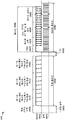
도 10 은 CxMi 버스에 접속되고 프로세싱 회로 (1002) 를 채용한 장치의 하드웨어 구현의 단순화된 예를 도시한 다이어그램 (1000) 이다. 일 예에 있어서, 그 장치는, 데이터 인코딩, 포맷팅 및/또는 데이터를 송신하는 것을 위해 사용될 수도 있는 CxMi 게이트웨이들 (420, 440, 460) 과 같은 컴포넌트들, 모듈들 또는 회로들이 장비된 하나 이상의 IC 디바이스들 (402, 404, 및/또는 406) (도 4 참조) 을 포함할 수도 있다. 프로세싱 회로 (1002) 의 하나 이상의 인스턴스들 또는 변형들은 장치 (400) 에 및/또는 IC 디바이스들 (402, 404, 및/또는 406) 중 하나 이상에 배치될 수도 있다. 프로세싱 회로 (1002) 는 버스 (1020) 에 의해 일반적으로 표현되는 버스 아키텍처로 구현될 수도 있다. 버스 (1020) 는 프로세싱 회로 (1002) 의 특정 어플리케이션 및 전체 설계 제약들에 의존하는 임의의 수의 상호접속 버스들 및 브리지들을 포함할 수도 있다. 버스 (1020) 는 프로세서 (1016), 모듈들 또는 회로들 (1004, 1006, 1008, 및 1010), 커넥터들 또는 와이어들 (1014) 을 구동하도록 구성가능한 라인 드라이버들 (1012), 및 컴퓨터 판독가능 저장 매체 (1018) 에 의해 표현된 하나 이상의 프로세서들 및/또는 하드웨어 모듈들을 포함한 다양한 회로들을 함께 링크시킨다. 버스 (1020) 는 또한, 당업계에 널리 공지되고 따라서 어떠한 추가로 설명되지 않을 타이밍 소스들, 주변기기들, 전압 레귤레이터들, 및 전력 관리 회로들과 같은 다양한 다른 회로들을 링크시킬 수도 있다.10 is a diagram 1000 illustrating a simplified example of a hardware implementation of a device connected to a CxMi bus and employing a
프로세서 (1016) 는 마이크로 프로세서, 제어기, 디지털 신호 프로세서, 시퀀서, 상태 머신 등을 포함할 수도 있다. 프로세서 (1016) 는 컴퓨터 판독가능 저장 매체 (1016) 상에 저장된 소프트웨어의 실행을 포함한 일반 프로세싱을 책임진다. 소프트웨어는, 프로세서 (1016) 에 의해 실행될 경우, 프로세싱 회로 (1002) 로 하여금 임의의 특정 장치에 대해 상기 설명된 다양한 기능들을 수행하게 한다. 컴퓨터 판독가능 저장 매체 (1018) 는 또한, 소프트웨어를 실행할 경우 프로세서 (1016) 에 의해 조작되는 데이터를 저장하는데 사용될 수도 있다. 프로세싱 회로 (1002) 는 모듈들 (1004, 1006, 1008, 및 1010) 중 적어도 하나를 더 포함한다. 특정 모듈들 (1004, 1006, 1008, 및/또는 1010) 은 컴퓨터 판독가능 저장 매체 (1018) 에 상주/저장된, 프로세서 (1016) 에서 구동하는 소프트웨어 모듈들, 프로세서 (1016) 에 커플링된 하나 이상의 하드웨어 모듈들, 또는 이들의 일부 조합일 수도 있다.The
일 구성에 있어서, 무선 통신을 위한 장치 (1000) 는 제 1 전압 레벨에서 데이터 신호를 구동함으로써 통신 링크의 제어를 위해 경합하는 수단 (1004, 1006, 1012), 일 시간 주기 동안 데이터 신호 및 클록 신호를 모니터링하는 수단 (1008, 1012), 데이터 신호 또는 클록 신호의 전압이 제 1 시간 주기의 만료 시에 제 1 전압 레벨에 있지 않으면 통신 링크의 제어를 양보하는 수단 (1004, 1006, 1012), 데이터 신호의 전압이 시간 주기의 만료 시에 제 1 전압 레벨에 있으면 제 2 전압 레벨에서 데이터 신호를 구동함으로써 통신 링크 (1014) 상의 제어를 어써트하는 수단 (1004, 1006, 1012), 및 통신 링크의 제어를 어써트한 이후 통신 상의 메시지를 송신하는 수단 (1010, 1008 및 1012) 을 포함한다.In one configuration, an
전술한 수단들은, 예를 들어, 프로세싱 회로 (226, 246, 266 및/또는 282) (도 2 참조), 게이트웨이들 (220, 240, 260, 280) (도 2 참조), 게이트웨이들 (420, 440, 460) (도 4 참조) 및 저장 매체들 (286) (도 2 참조) 의 일부 조합을 사용하여 구현될 수도 있다.2),
개시된 프로세스들에 있어서의 단계들의 특정 순서 또는 계위는 예시적인 접근법들의 예시임이 이해된다. 설계 선호도들에 기초하여, 프로세스들에 있어서의 단계들의 특정 순서 또는 계위가 재배열될 수도 있음이 이해된다. 첨부한 방법 청구항들은 다양한 단계들의 엘리먼트들을 샘플 순서로 제시하며, 제시된 특정 순서 또는 계위로 한정되도록 의도되지 않는다.It is understood that the specific order or hierarchy of steps in the disclosed processes is exemplary of exemplary approaches. It is understood that, based on design preferences, a particular order or hierarchy of steps in the processes may be rearranged. The appended method claims present the elements of the various steps in a sample order, and are not intended to be limited to the specific sequence or order presented.
상기 설명은 당업자로 하여금 본 명세서에서 설명된 다양한 양태들을 실시할 수 있도록 제공된다. 이들 양태들에 대한 다양한 수정들은 당업자에게 용이하게 자명할 것이며, 본 명세서에서 정의된 일반적인 원리들은 다른 양태들에 적용될 수도 있다. 따라서, 청구항들은 본 명세서에서 설명된 양태들로 한정되도록 의도되지 않지만, 랭귀지 청구항들과 부합하는 충분한 범위를 부여받아야 하며, 여기서, 단수로의 엘리먼트들에 대한 언급은 명확하게 그렇게 서술되지 않으면 "하나 또는 단지 하나만" 을 의미하도록 의도되지 않고 오히려 "하나 이상" 을 의미하도록 의도된다. 명확하게 달리 서술되지 않으면, 용어 "일부" 는 하나 이상을 지칭한다. 당업자에게 공지되어 있거나 나중에 공지되게 되는 본 개시 전반에 걸쳐 설명된 다양한 양태들의 엘리먼트들에 대한 모든 구조적 및 기능적 균등물들은 본 명세서에 참조로 명확히 통합되고 청구항들에 의해 포괄되도록 의도된다. 더욱이, 본 명세서에 개시된 어떤 것도, 그러한 개시가 청구항들에 명시적으로 기재되는지 여부에 무관하게 공중에 전용되도록 의도되지 않는다. 어떠한 청구항 엘리먼트도, 그 엘리먼트가 어구 "~를 위한 수단" 을 이용하여 명백하게 기재되지 않는다면 수단 플러스 기능으로서 해석되지 않아야 한다.The description is provided to enable those skilled in the art to practice the various aspects described herein. Various modifications to these aspects will be readily apparent to those skilled in the art, and the generic principles defined herein may be applied to other aspects. Accordingly, the claims are not intended to be limited to the aspects described herein, but are to be accorded the full breadth of conformity with the language claims, wherein references to elements in singular < RTI ID = Quot; is intended to mean " one or more "rather than " only one ". Unless specifically stated otherwise, the term "part" refers to one or more. All structural and functional equivalents to the elements of the various aspects disclosed throughout this disclosure which are known to those skilled in the art or which will be known later are expressly incorporated herein by reference and are intended to be encompassed by the claims. Moreover, nothing disclosed herein is intended to be dedicated to the public regardless of whether such disclosure is expressly set forth in the claims. No claim element should be construed as a means plus function unless the element is explicitly stated using the phrase " means for ".
Claims (40)
제 1 전압 레벨에서 데이터 신호를 구동함으로써 통신 링크의 제어를 위해 경합하는 단계;
제 1 시간 주기 동안 상기 데이터 신호 및 클록 신호를 모니터링하는 단계;
상기 데이터 신호 또는 상기 클록 신호의 전압이 상기 제 1 시간 주기의 만료 시에 상기 제 1 전압 레벨에 있지 않으면 상기 통신 링크의 제어를 양보하는 단계;
상기 데이터 신호 및 상기 클록 신호의 전압들이 상기 제 1 시간 주기의 만료 시에 상기 제 1 전압 레벨에 있으면 제 2 전압 레벨에서 상기 데이터 신호를 구동함으로써 상기 통신 링크 상의 제어를 어써트(assert)하는 단계; 및
상기 통신 링크의 제어를 어써트한 이후 통신 상의 메시지를 송신하는 단계를 포함하고,
상기 제 1 시간 주기는 상기 메시지의 우선순위에 대응하는 지속기간을 갖는, 노드들 사이에서 통신하기 위한 방법.CLAIMS What is claimed is: 1. A method for communicating between nodes in a device,
Competing for control of the communication link by driving a data signal at a first voltage level;
Monitoring the data signal and the clock signal during a first time period;
Yielding control of the communication link if the voltage of the data signal or the clock signal is not at the first voltage level at the expiration of the first time period;
Asserting control over the communication link by driving the data signal at a second voltage level if the voltages of the data signal and the clock signal are at the first voltage level at the expiration of the first time period ; And
Transmitting a message on communication after asserting control of the communication link,
Wherein the first time period has a duration corresponding to a priority of the message.
상기 통신 링크의 제어를 위해 경합하는 단계는,
상기 제 1 전압 레벨에서 상기 데이터 신호를 구동하기 이전 제 2 시간 주기 동안 상기 통신 링크의 상기 데이터 신호 및 상기 클록 신호가 유휴상태이었음을 결정하는 단계를 포함하는, 노드들 사이에서 통신하기 위한 방법.The method according to claim 1,
Wherein competing for control of the communication link comprises:
And determining that the data signal and the clock signal of the communication link are idle during a second time period prior to driving the data signal at the first voltage level.
상기 제 2 시간 주기는 상기 통신 링크 상으로 상기 메시지를 송신하도록 구성된 노드와 연관된 우선순위 또는 상기 메시지의 우선순위에 기초하여 계산되며,
상기 제 2 시간 주기는 상위 우선순위들에 대해 더 짧은, 노드들 사이에서 통신하기 위한 방법.3. The method of claim 2,
Wherein the second time period is calculated based on a priority associated with a node configured to transmit the message on the communication link or a priority of the message,
And wherein the second time period is shorter for higher priorities.
상기 제 1 시간 주기는 상기 통신 링크의 제어를 위해 경합하는 2 이상의 노드들에 대해 상이하게 정의되는, 노드들 사이에서 통신하기 위한 방법.The method according to claim 1,
Wherein the first time period is defined differently for two or more competing nodes for control of the communication link.
상기 제 1 시간 주기는 상기 통신 링크와 연관된 타이밍 활동들을 위해 정의된 송신 타이밍 유닛의 배수로서 계산되며,
상기 데이터 신호는 1 미만의 송신 타이밍 유닛 동안 상기 제 1 전압 레벨에서 구동되는, 노드들 사이에서 통신하기 위한 방법.The method according to claim 1,
Wherein the first time period is calculated as a multiple of a transmission timing unit defined for timing activities associated with the communication link,
Wherein the data signal is driven at the first voltage level during less than one transmission timing unit.
상기 통신 링크는 상이한 집적회로 디바이스들 상에 위치된 노드들을 접속시키는, 노드들 사이에서 통신하기 위한 방법.6. The method of claim 5,
Wherein the communication link connects nodes located on different integrated circuit devices.
상기 상이한 집적회로 디바이스들 상에 위치된 상기 노드들은 상이한 내부 클록 레이트들로 동작하고,
상기 송신 타이밍 유닛은 내부 클록들의 가장 느린 클록 주기보다 크거나 같은, 노드들 사이에서 통신하기 위한 방법.The method according to claim 6,
The nodes located on the different integrated circuit devices operate at different internal clock rates,
Wherein the transmit timing unit is greater than or equal to the slowest clock period of internal clocks.
상기 제 1 시간 주기는 상기 통신 링크 상으로 상기 메시지를 송신하도록 구성된 노드의 어드레스와 상기 메시지의 우선순위의 가중 합으로서 계산되며,
상기 제 1 시간 주기는 상위 우선순위 메시지들 또는 상위 우선순위 노드들에 대해 더 짧은, 노드들 사이에서 통신하기 위한 방법.The method according to claim 1,
Wherein the first time period is calculated as a weighted sum of an address of a node configured to transmit the message on the communication link and a priority of the message,
Wherein the first time period is shorter for higher priority messages or higher priority nodes.
상기 제 1 시간 주기 동안 상기 데이터 신호를 모니터링하는 단계는 상기 통신 링크 상으로 상기 메시지를 송신하도록 구성된 노드로 하여금 고 임피던스 상태로 진입하게 하는 단계를 포함하는, 노드들 사이에서 통신하기 위한 방법.The method according to claim 1,
Wherein monitoring the data signal during the first time period comprises causing a node configured to transmit the message on the communication link to enter a high impedance state.
상기 통신 링크의 제어는 상기 데이터 신호 및 상기 클록 신호의 제어를 포함하는, 노드들 사이에서 통신하기 위한 방법.The method according to claim 1,
Wherein control of the communication link comprises control of the data signal and the clock signal.
제 1 시간 주기 동안 상기 데이터 신호 및 클록 신호를 모니터링하는 수단;
상기 데이터 신호 또는 상기 클록 신호의 전압이 상기 제 1 시간 주기의 만료 시에 상기 제 1 전압 레벨에 있지 않으면 상기 통신 링크의 제어를 양보하는 수단;
상기 데이터 신호 및 상기 클록 신호의 전압들이 상기 제 1 시간 주기의 만료 시에 상기 제 1 전압 레벨에 있으면 제 2 전압 레벨에서 상기 데이터 신호를 구동함으로써 상기 통신 링크 상의 제어를 어써트하는 수단; 및
상기 통신 링크의 제어를 어써트한 이후 통신 상의 메시지를 송신하는 수단을 포함하고,
상기 제 1 시간 주기는 상기 메시지의 우선순위에 대응하는 지속기간을 갖는, 장치.Means for contending for control of the communication link by driving a data signal at a first voltage level;
Means for monitoring the data signal and the clock signal during a first time period;
Means for yielding control of the communication link if the voltage of the data signal or the clock signal is not at the first voltage level at the expiration of the first time period;
Means for asserting control on the communication link by driving the data signal at a second voltage level if the voltages of the data signal and the clock signal are at the first voltage level at the expiration of the first time period; And
Means for transmitting a message on a communication after asserting control of the communication link,
Wherein the first time period has a duration corresponding to a priority of the message.
상기 통신 링크의 제어를 위해 경합하는 수단은 상기 통신 링크의 상기 데이터 신호 및 상기 클록 신호가 상기 제 1 전압 레벨에서 상기 데이터 신호를 구동하기 이전 제 2 시간 주기 동안 유휴상태이었음을 결정하도록 구성되는, 장치.12. The method of claim 11,
Wherein the means for contention for control of the communication link is configured to determine that the data signal of the communication link and the clock signal are idle during a second time period prior to driving the data signal at the first voltage level. Device.
상기 제 2 시간 주기는 상기 통신 링크 상으로 상기 메시지를 송신하도록 구성된 노드와 연관된 우선순위 또는 상기 메시지의 우선순위에 기초하여 계산되며,
상기 제 2 시간 주기는 상위 우선순위들에 대해 더 짧은, 장치.13. The method of claim 12,
Wherein the second time period is calculated based on a priority associated with a node configured to transmit the message on the communication link or a priority of the message,
Wherein the second time period is shorter for higher priorities.
상기 제 1 시간 주기는 상기 통신 링크의 제어를 위해 경합하는 2 이상의 노드들에 대해 상이하게 정의되는, 장치.12. The method of claim 11,
Wherein the first time period is defined differently for two or more competing nodes for control of the communication link.
상기 제 1 시간 주기는 상기 통신 링크와 연관된 타이밍 활동들을 위해 정의된 송신 타이밍 유닛의 배수로서 계산되며,
상기 데이터 신호는 1 미만의 송신 타이밍 유닛 동안 상기 제 1 전압 레벨에서 구동되는, 장치.12. The method of claim 11,
Wherein the first time period is calculated as a multiple of a transmission timing unit defined for timing activities associated with the communication link,
Wherein the data signal is driven at the first voltage level for less than one transmission timing unit.
상기 통신 링크는 상이한 집적회로 디바이스들 상에 위치된 노드들을 접속시키는, 장치.16. The method of claim 15,
Wherein the communication link connects nodes located on different integrated circuit devices.
상기 상이한 집적회로 디바이스들 상에 위치된 상기 노드들은 상이한 내부 클록 레이트들로 동작하고,
상기 송신 타이밍 유닛은 내부 클록들의 가장 느린 클록 주기보다 크거나 같은, 장치.17. The method of claim 16,
The nodes located on the different integrated circuit devices operate at different internal clock rates,
Wherein the transmit timing unit is greater than or equal to the slowest clock cycle of the internal clocks.
상기 제 1 시간 주기는 상기 통신 링크 상으로 상기 메시지를 송신하도록 구성된 노드의 어드레스와 상기 메시지의 우선순위의 가중 합으로서 계산되며,
상기 제 1 시간 주기는 상위 우선순위 메시지들 또는 상위 우선순위 노드들에 대해 더 짧은, 장치.12. The method of claim 11,
Wherein the first time period is calculated as a weighted sum of an address of a node configured to transmit the message on the communication link and a priority of the message,
Wherein the first time period is shorter for higher priority messages or higher priority nodes.
상기 제 1 시간 주기 동안 상기 데이터 신호를 모니터링하는 수단은 상기 통신 링크 상으로 상기 메시지를 송신하도록 구성된 노드로 하여금 고 임피던스 상태로 진입하게 하도록 구성되는, 장치.12. The method of claim 11,
Wherein the means for monitoring the data signal during the first time period is configured to cause a node configured to transmit the message on the communication link to enter a high impedance state.
상기 통신 링크의 제어는 상기 데이터 신호 및 상기 클록 신호의 제어를 포함하는, 장치.12. The method of claim 11,
Wherein control of the communication link comprises control of the data signal and the clock signal.
상기 프로세싱 회로는,
제 1 전압 레벨에서 데이터 신호를 구동함으로써 통신 링크의 제어를 위해 경합하고;
제 1 시간 주기 동안 상기 데이터 신호 및 클록 신호를 모니터링하고;
상기 데이터 신호 또는 상기 클록 신호의 전압이 상기 제 1 시간 주기의 만료 시에 상기 제 1 전압 레벨에 있지 않으면 상기 통신 링크의 제어를 양보하고;
상기 데이터 신호 및 상기 클록 신호의 전압들이 상기 제 1 시간 주기의 만료 시에 상기 제 1 전압 레벨에 있으면 제 2 전압 레벨에서 상기 데이터 신호를 구동함으로써 상기 통신 링크 상의 제어를 어써트하며; 그리고
상기 통신 링크의 제어를 어써트한 이후 통신 상의 메시지를 송신하도록
구성되고,
상기 제 1 시간 주기는 상기 메시지의 우선순위에 대응하는 지속기간을 갖는, 장치.Processing circuit,
The processing circuit comprising:
Compete for control of the communication link by driving a data signal at a first voltage level;
Monitoring the data signal and the clock signal during a first time period;
Yields control of the communication link if the voltage of the data signal or the clock signal is not at the first voltage level at the expiration of the first time period;
Assert control over the communication link by driving the data signal at a second voltage level if the voltages of the data signal and the clock signal are at the first voltage level at the expiration of the first time period; And
To send a message on the communication after asserting control of the communication link
Respectively,
Wherein the first time period has a duration corresponding to a priority of the message.
상기 프로세싱 회로는, 상기 통신 링크의 상기 데이터 신호 및 상기 클록 신호가 상기 제 1 전압 레벨에서 상기 데이터 신호를 구동하기 이전 제 2 시간 주기 동안 유휴상태이었음을 결정하도록 구성되는, 장치.22. The method of claim 21,
Wherein the processing circuit is configured to determine that the data signal of the communication link and the clock signal are idle for a second period of time before driving the data signal at the first voltage level.
상기 제 2 시간 주기는 상기 통신 링크 상으로 상기 메시지를 송신하도록 구성된 노드와 연관된 우선순위 또는 상기 메시지의 우선순위에 기초하여 계산되며,
상기 제 2 시간 주기는 상위 우선순위들에 대해 더 짧은, 장치.23. The method of claim 22,
Wherein the second time period is calculated based on a priority associated with a node configured to transmit the message on the communication link or a priority of the message,
Wherein the second time period is shorter for higher priorities.
상기 제 1 시간 주기는 상기 통신 링크의 제어를 위해 경합하는 2 이상의 노드들에 대해 상이하게 정의되는, 장치.22. The method of claim 21,
Wherein the first time period is defined differently for two or more competing nodes for control of the communication link.
상기 제 1 시간 주기는 상기 통신 링크와 연관된 타이밍 활동들을 위해 정의된 송신 타이밍 유닛의 배수로서 계산되며,
상기 데이터 신호는 1 미만의 송신 타이밍 유닛 동안 상기 제 1 전압 레벨에서 구동되는, 장치.22. The method of claim 21,
Wherein the first time period is calculated as a multiple of a transmission timing unit defined for timing activities associated with the communication link,
Wherein the data signal is driven at the first voltage level for less than one transmission timing unit.
상기 통신 링크는 상이한 집적회로 디바이스들 상에 위치된 노드들을 접속시키는, 장치.26. The method of claim 25,
Wherein the communication link connects nodes located on different integrated circuit devices.
상기 상이한 집적회로 디바이스들 상에 위치된 상기 노드들은 상이한 내부 클록 레이트들로 동작하고,
상기 송신 타이밍 유닛은 내부 클록들의 가장 느린 클록 주기보다 크거나 같은, 장치.27. The method of claim 26,
The nodes located on the different integrated circuit devices operate at different internal clock rates,
Wherein the transmit timing unit is greater than or equal to the slowest clock cycle of the internal clocks.
상기 제 1 시간 주기는 상기 통신 링크 상으로 상기 메시지를 송신하도록 구성된 노드의 어드레스와 상기 메시지의 우선순위의 가중 합으로서 계산되며,
상기 제 1 시간 주기는 상위 우선순위 메시지들 또는 상위 우선순위 노드들에 대해 더 짧은, 장치.22. The method of claim 21,
Wherein the first time period is calculated as a weighted sum of an address of a node configured to transmit the message on the communication link and a priority of the message,
Wherein the first time period is shorter for higher priority messages or higher priority nodes.
상기 프로세싱 회로는, 상기 통신 링크 상으로 상기 메시지를 송신하도록 구성된 노드로 하여금 상기 제 1 시간 주기 동안 상기 데이터 신호를 모니터링하면서 고 임피던스 상태로 진입하게 하도록 구성되는, 장치.22. The method of claim 21,
Wherein the processing circuit is configured to cause a node configured to transmit the message on the communication link to enter a high impedance state while monitoring the data signal for the first time period.
상기 통신 링크의 제어는 상기 데이터 신호 및 상기 클록 신호의 제어를 포함하는, 장치.22. The method of claim 21,
Wherein control of the communication link comprises control of the data signal and the clock signal.
상기 명령들은, 적어도 하나의 프로세싱 회로에 의해 실행될 경우, 상기 적어도 하나의 프로세싱 회로로 하여금
제 1 전압 레벨에서 데이터 신호를 구동함으로써 통신 링크의 제어를 위해 경합하게 하고;
제 1 시간 주기 동안 상기 데이터 신호 및 클록 신호를 모니터링하게 하고;
상기 데이터 신호 또는 상기 클록 신호의 전압이 상기 제 1 시간 주기의 만료 시에 상기 제 1 전압 레벨에 있지 않으면 상기 통신 링크의 제어를 양보하게 하고;
상기 데이터 신호 및 상기 클록 신호의 전압들이 상기 제 1 시간 주기의 만료 시에 상기 제 1 전압 레벨에 있으면 제 2 전압 레벨에서 상기 데이터 신호를 구동함으로써 상기 통신 링크 상의 제어를 어써트하게 하며; 그리고
상기 통신 링크의 제어를 어써트한 이후 통신 상의 메시지를 송신하게 하고,
상기 제 1 시간 주기는 상기 메시지의 우선순위에 대응하는 지속기간을 갖는, 비-일시적인 머신 판독가능 저장 매체.18. A non-transient machine-readable storage medium having stored thereon instructions,
Wherein the instructions, when executed by the at least one processing circuit, cause the at least one processing circuit
Compete for control of the communication link by driving a data signal at a first voltage level;
Monitor the data signal and the clock signal for a first time period;
Yielding control of the communication link if the voltage of the data signal or the clock signal is not at the first voltage level at the expiration of the first time period;
Assert control over the communication link by driving the data signal at a second voltage level if the voltages of the data signal and the clock signal are at the first voltage level at the expiration of the first time period; And
After the control of the communication link is asserted, causes a message on communication to be transmitted,
The first time period having a duration corresponding to a priority of the message.
상기 명령들은 상기 적어도 하나의 프로세싱 회로로 하여금
상기 제 1 전압 레벨에서 상기 데이터 신호를 구동하기 이전 제 2 시간 주기 동안 상기 통신 링크의 상기 데이터 신호 및 상기 클록 신호가 유휴상태이었음을 결정하게 하는, 비-일시적인 머신 판독가능 저장 매체.32. The method of claim 31,
The instructions cause the at least one processing circuit
To cause the data signal and the clock signal of the communication link to be in an idle state during a second time period prior to driving the data signal at the first voltage level.
상기 제 2 시간 주기는 상기 통신 링크 상으로 상기 메시지를 송신하도록 구성된 노드와 연관된 우선순위 또는 상기 메시지의 우선순위에 기초하여 계산되며,
상기 제 2 시간 주기는 상위 우선순위들에 대해 더 짧은, 비-일시적인 머신 판독가능 저장 매체.33. The method of claim 32,
Wherein the second time period is calculated based on a priority associated with a node configured to transmit the message on the communication link or a priority of the message,
And the second time period is shorter for higher priorities.
상기 제 1 시간 주기는 상기 통신 링크의 제어를 위해 경합하는 2 이상의 노드들에 대해 상이하게 정의되는, 비-일시적인 머신 판독가능 저장 매체.32. The method of claim 31,
Wherein the first time period is defined differently for two or more competing nodes for control of the communication link.
상기 제 1 시간 주기는 상기 통신 링크와 연관된 타이밍 활동들을 위해 정의된 송신 타이밍 유닛의 배수로서 계산되며,
상기 데이터 신호는 1 미만의 송신 타이밍 유닛 동안 상기 제 1 전압 레벨에서 구동되는, 비-일시적인 머신 판독가능 저장 매체.32. The method of claim 31,
Wherein the first time period is calculated as a multiple of a transmission timing unit defined for timing activities associated with the communication link,
Wherein the data signal is driven at the first voltage level during less than one transmission timing unit.
상기 통신 링크는 상이한 집적회로 디바이스들 상에 위치된 노드들을 접속시키는, 비-일시적인 머신 판독가능 저장 매체.36. The method of claim 35,
Wherein the communication link connects nodes located on different integrated circuit devices.
상기 상이한 집적회로 디바이스들 상에 위치된 상기 노드들은 상이한 내부 클록 레이트들로 동작하고,
상기 송신 타이밍 유닛은 내부 클록들의 가장 느린 클록 주기보다 크거나 같은, 비-일시적인 머신 판독가능 저장 매체.37. The method of claim 36,
The nodes located on the different integrated circuit devices operate at different internal clock rates,
Wherein the transmit timing unit is greater than or equal to the slowest clock period of the internal clocks.
상기 제 1 시간 주기는 상기 통신 링크 상으로 상기 메시지를 송신하도록 구성된 노드의 어드레스와 상기 메시지의 우선순위의 가중 합으로서 계산되며,
상기 제 1 시간 주기는 상위 우선순위 메시지들 또는 상위 우선순위 노드들에 대해 더 짧은, 비-일시적인 머신 판독가능 저장 매체.32. The method of claim 31,
Wherein the first time period is calculated as a weighted sum of an address of a node configured to transmit the message on the communication link and a priority of the message,
Wherein the first time period is shorter for higher priority messages or higher priority nodes.
상기 명령들은 상기 적어도 하나의 프로세싱 회로로 하여금
상기 통신 링크 상으로 상기 메시지를 송신하도록 구성된 노드가 상기 제 1 시간 주기 동안 상기 데이터 신호를 모니터링하면서 고 임피던스 상태로 진입하게 하도록 하는, 비-일시적인 머신 판독가능 저장 매체.32. The method of claim 31,
The instructions cause the at least one processing circuit
And cause a node configured to transmit the message on the communication link to enter a high impedance state while monitoring the data signal during the first time period.
상기 통신 링크의 제어는 상기 데이터 신호 및 상기 클록 신호의 제어를 포함하는, 비-일시적인 머신 판독가능 저장 매체.32. The method of claim 31,
Wherein control of the communication link comprises control of the data signal and the clock signal.
Applications Claiming Priority (3)
| Application Number | Priority Date | Filing Date | Title |
|---|---|---|---|
| US14/089,550 US9497710B2 (en) | 2013-11-25 | 2013-11-25 | Multipoint interface shortest pulse width priority resolution |
| US14/089,550 | 2013-11-25 | ||
| PCT/US2014/066814 WO2015077562A1 (en) | 2013-11-25 | 2014-11-21 | Multipoint interface shortest pulse width priority resolution |
Publications (1)
| Publication Number | Publication Date |
|---|---|
| KR20160091373A true KR20160091373A (en) | 2016-08-02 |
Family
ID=52103172
Family Applications (1)
| Application Number | Title | Priority Date | Filing Date |
|---|---|---|---|
| KR1020167016886A KR20160091373A (en) | 2013-11-25 | 2014-11-21 | Multipoint interface shortest pulse width priority resolution |
Country Status (6)
| Country | Link |
|---|---|
| US (1) | US9497710B2 (en) |
| EP (1) | EP3074874B1 (en) |
| JP (1) | JP2016541063A (en) |
| KR (1) | KR20160091373A (en) |
| CN (1) | CN105993007B (en) |
| WO (1) | WO2015077562A1 (en) |
Cited By (1)
| Publication number | Priority date | Publication date | Assignee | Title |
|---|---|---|---|---|
| WO2022211204A1 (en) * | 2021-03-31 | 2022-10-06 | 주식회사 럭스로보 | Module assembly and multi-master communication method therefor |
Families Citing this family (6)
| Publication number | Priority date | Publication date | Assignee | Title |
|---|---|---|---|---|
| US9154130B2 (en) * | 2014-01-14 | 2015-10-06 | Analog Devices, Inc. | Four-state input detection circuitry |
| US20170075843A1 (en) | 2015-09-10 | 2017-03-16 | Qualcomm Incorporated | Unified systems and methods for interchip and intrachip node communication |
| US20170329738A1 (en) * | 2016-05-10 | 2017-11-16 | Qualcomm Incorporated | Digital signaling schemes for line multiplexed uart flow control |
| US20190171588A1 (en) * | 2017-12-05 | 2019-06-06 | Qualcomm Incorporated | Multi-point virtual general-purpose input/output (mp-vgi) for low latency event messaging |
| US20200233829A1 (en) * | 2019-01-22 | 2020-07-23 | Qualcomm Incorporated | Multi-lane system power management interface |
| CN114363107B (en) * | 2021-12-29 | 2024-05-07 | 上海联影医疗科技股份有限公司 | Time-sharing scheduling method and system for controller local area network bus |
Family Cites Families (28)
| Publication number | Priority date | Publication date | Assignee | Title |
|---|---|---|---|---|
| US4359731A (en) * | 1980-08-22 | 1982-11-16 | Phillips Petroleum Company | Communication link contention resolution system |
| US4670872A (en) * | 1985-07-02 | 1987-06-02 | Phillips Petroleum Company | Communication link contention resolution system |
| GB2232855B (en) | 1989-06-07 | 1993-10-20 | Secr Defence | Computer network access control system |
| US5555545A (en) * | 1994-06-23 | 1996-09-10 | Gemtek Technology Co., Ltd. | Connecting apparatus for interconnection between serial data transmission devices |
| JPH0823585A (en) | 1994-07-06 | 1996-01-23 | Toshiba Corp | Job site monitoring control panel system |
| JP2850282B2 (en) * | 1994-07-06 | 1999-01-27 | 日本コロムビア株式会社 | Communication device |
| US5710910A (en) * | 1994-09-30 | 1998-01-20 | University Of Washington | Asynchronous self-tuning clock domains and method for transferring data among domains |
| JPH09244991A (en) | 1996-03-11 | 1997-09-19 | Commuter Herikoputa Senshin Gijutsu Kenkyusho:Kk | Distributed bus arbiter and bus arbitration method |
| US6002669A (en) | 1996-03-26 | 1999-12-14 | White; Darryl C. | Efficient, multi-purpose network data communications protocol |
| KR100201325B1 (en) * | 1996-03-30 | 1999-06-15 | 유기범 | Method of rising frequency of bus clock in a multiprocessor system |
| US6092137A (en) * | 1997-11-26 | 2000-07-18 | Industrial Technology Research Institute | Fair data bus arbitration system which assigns adjustable priority values to competing sources |
| TW468110B (en) | 1998-05-04 | 2001-12-11 | Koninkl Philips Electronics Nv | Electronic apparatus with a bus |
| US6411218B1 (en) * | 1999-01-22 | 2002-06-25 | Koninklijke Philips Electronics N.V. | Priority-encoding device selection using variable arbitrary rankings |
| JP2000250851A (en) | 1999-03-03 | 2000-09-14 | Sony Corp | Method and system for arbitrating bus |
| US6636914B1 (en) * | 1999-11-05 | 2003-10-21 | Apple Computer, Inc. | Method and apparatus for arbitration and fairness on a full-duplex bus using dual phases |
| US6629177B1 (en) * | 1999-12-27 | 2003-09-30 | Intel Corporation | Arbitrating requests on computer buses |
| JP4741122B2 (en) * | 2001-09-07 | 2011-08-03 | 富士通セミコンダクター株式会社 | Semiconductor device and data transfer method |
| JP2003196229A (en) * | 2001-12-28 | 2003-07-11 | Sony Corp | Data transfer method in bus interface and bus interface |
| DE102004024849B4 (en) * | 2003-05-23 | 2008-11-27 | Samsung Electronics Co., Ltd. | Arbitration unit, associated bus system and Arbitrierungsverfahren |
| KR100626362B1 (en) * | 2003-05-23 | 2006-09-20 | 삼성전자주식회사 | Arbiter and method for arbitrating high-performance bandwidth system bus and bus system having arbiter |
| JP4615965B2 (en) * | 2003-11-05 | 2011-01-19 | ルネサスエレクトロニクス株式会社 | Communication system, information processing apparatus having the communication system, and control |
| US7143220B2 (en) | 2004-03-10 | 2006-11-28 | Intel Corporation | Apparatus and method for granting concurrent ownership to support heterogeneous agents in on-chip busses having different grant-to-valid latencies |
| JP2006049948A (en) * | 2004-07-30 | 2006-02-16 | Seiko Epson Corp | Data transfer control apparatus, electronic apparatus, and data transfer control method |
| KR100868766B1 (en) * | 2007-01-31 | 2008-11-17 | 삼성전자주식회사 | Method and apparatus for determining priority in direct memory access apparatus having multiple direct memory access requesting blocks |
| US8068790B2 (en) | 2007-01-31 | 2011-11-29 | Broadcom Corporation | RF bus access protocol and transceiver |
| US8867573B2 (en) * | 2007-04-23 | 2014-10-21 | Nokia Corporation | Transferring data between asynchronous clock domains |
| US9135197B2 (en) | 2009-07-29 | 2015-09-15 | Qualcomm Incorporated | Asynchronous interface for multi-radio coexistence manager |
| US9134919B2 (en) * | 2012-03-29 | 2015-09-15 | Samsung Electronics Co., Ltd. | Memory device including priority information and method of operating the same |
-
2013
- 2013-11-25 US US14/089,550 patent/US9497710B2/en active Active
-
2014
- 2014-11-21 KR KR1020167016886A patent/KR20160091373A/en not_active Application Discontinuation
- 2014-11-21 EP EP14812844.0A patent/EP3074874B1/en active Active
- 2014-11-21 WO PCT/US2014/066814 patent/WO2015077562A1/en active Application Filing
- 2014-11-21 CN CN201480064263.7A patent/CN105993007B/en active Active
- 2014-11-21 JP JP2016533115A patent/JP2016541063A/en active Pending
Cited By (2)
| Publication number | Priority date | Publication date | Assignee | Title |
|---|---|---|---|---|
| WO2022211204A1 (en) * | 2021-03-31 | 2022-10-06 | 주식회사 럭스로보 | Module assembly and multi-master communication method therefor |
| KR20220135775A (en) * | 2021-03-31 | 2022-10-07 | 주식회사 럭스로보 | A module assembly and multi-master communication method thereof |
Also Published As
| Publication number | Publication date |
|---|---|
| US20150146624A1 (en) | 2015-05-28 |
| CN105993007A (en) | 2016-10-05 |
| EP3074874B1 (en) | 2020-02-12 |
| EP3074874A1 (en) | 2016-10-05 |
| CN105993007B (en) | 2019-06-25 |
| WO2015077562A1 (en) | 2015-05-28 |
| JP2016541063A (en) | 2016-12-28 |
| US9497710B2 (en) | 2016-11-15 |
Similar Documents
| Publication | Publication Date | Title |
|---|---|---|
| EP3074874B1 (en) | Multipoint interface shortest pulse width priority resolution | |
| US8744356B2 (en) | Apparatuses and methods for coordination between plurality of co-located wireless communication modules via one wire | |
| CN106063198B (en) | Subscriber station of a bus system and method for improving the transmission quality in a bus system | |
| CN108243017B (en) | Broadcast implementation method, device and equipment | |
| US20130290580A1 (en) | Method and device for serial data transmission at a switchable data rate | |
| KR20160107247A (en) | Camera control interface extension with in-band interrupt | |
| US11102031B2 (en) | Flexible data rate handling in data bus receiver | |
| JP5174624B2 (en) | Wireless communication system, wireless communication terminal, and wireless base station | |
| KR20170110610A (en) | Receive clock calibration for a serial bus | |
| KR101532332B1 (en) | A high speed data transmission method and corresponding devices | |
| CN109996325B (en) | Clock synchronization system and method of wireless sensor network | |
| CN112422153B (en) | Method and system for processing data reception after detecting collisions at a shared transmission medium | |
| JP2009206749A (en) | Multi-hop wireless network system | |
| WO2017065923A1 (en) | Methods to avoid i2c void message in i3c | |
| US20200201808A1 (en) | Time-division multiplexing (tdm) data transfer on serial interfaces | |
| KR20160047484A (en) | Method to minimize the number of irq lines from peripherals to one wire | |
| US11398925B2 (en) | Media access for time-sensitive and best efforts data packets, and related systems, methods and devices | |
| CN113940038B (en) | Subscriber station for a serial bus system and method for communication in a serial bus system | |
| CN112788622B (en) | Configuration method, device and equipment of sensing window | |
| CN111884751A (en) | Smart grid time synchronization method and device based on PTP | |
| FI127550B (en) | Slotted channel access in communications network | |
| US20180357067A1 (en) | In-band hardware reset for virtual general purpose input/output interface | |
| US7406555B2 (en) | Systems and methods for multiple input instrumentation buses | |
| JP6036859B2 (en) | Communication device | |
| KR20190078832A (en) | MAC protocol for wireless sensor network |
Legal Events
| Date | Code | Title | Description |
|---|---|---|---|
| WITN | Application deemed withdrawn, e.g. because no request for examination was filed or no examination fee was paid |