KR20160018781A - Camera control interface extension bus - Google Patents
Camera control interface extension bus Download PDFInfo
- Publication number
- KR20160018781A KR20160018781A KR1020167000592A KR20167000592A KR20160018781A KR 20160018781 A KR20160018781 A KR 20160018781A KR 1020167000592 A KR1020167000592 A KR 1020167000592A KR 20167000592 A KR20167000592 A KR 20167000592A KR 20160018781 A KR20160018781 A KR 20160018781A
- Authority
- KR
- South Korea
- Prior art keywords
- symbols
- serial bus
- wire serial
- sequence
- bus
- Prior art date
Links
Images


Classifications
-
- G—PHYSICS
- G06—COMPUTING; CALCULATING OR COUNTING
- G06F—ELECTRIC DIGITAL DATA PROCESSING
- G06F13/00—Interconnection of, or transfer of information or other signals between, memories, input/output devices or central processing units
- G06F13/38—Information transfer, e.g. on bus
- G06F13/42—Bus transfer protocol, e.g. handshake; Synchronisation
- G06F13/4282—Bus transfer protocol, e.g. handshake; Synchronisation on a serial bus, e.g. I2C bus, SPI bus
- G06F13/4291—Bus transfer protocol, e.g. handshake; Synchronisation on a serial bus, e.g. I2C bus, SPI bus using a clocked protocol
-
- G—PHYSICS
- G06—COMPUTING; CALCULATING OR COUNTING
- G06F—ELECTRIC DIGITAL DATA PROCESSING
- G06F13/00—Interconnection of, or transfer of information or other signals between, memories, input/output devices or central processing units
- G06F13/14—Handling requests for interconnection or transfer
- G06F13/36—Handling requests for interconnection or transfer for access to common bus or bus system
- G06F13/362—Handling requests for interconnection or transfer for access to common bus or bus system with centralised access control
- G06F13/364—Handling requests for interconnection or transfer for access to common bus or bus system with centralised access control using independent requests or grants, e.g. using separated request and grant lines
-
- G—PHYSICS
- G06—COMPUTING; CALCULATING OR COUNTING
- G06F—ELECTRIC DIGITAL DATA PROCESSING
- G06F13/00—Interconnection of, or transfer of information or other signals between, memories, input/output devices or central processing units
- G06F13/38—Information transfer, e.g. on bus
- G06F13/42—Bus transfer protocol, e.g. handshake; Synchronisation
- G06F13/4282—Bus transfer protocol, e.g. handshake; Synchronisation on a serial bus, e.g. I2C bus, SPI bus
- G06F13/4295—Bus transfer protocol, e.g. handshake; Synchronisation on a serial bus, e.g. I2C bus, SPI bus using an embedded synchronisation
-
- H—ELECTRICITY
- H04—ELECTRIC COMMUNICATION TECHNIQUE
- H04L—TRANSMISSION OF DIGITAL INFORMATION, e.g. TELEGRAPHIC COMMUNICATION
- H04L7/00—Arrangements for synchronising receiver with transmitter
- H04L7/02—Speed or phase control by the received code signals, the signals containing no special synchronisation information
- H04L7/033—Speed or phase control by the received code signals, the signals containing no special synchronisation information using the transitions of the received signal to control the phase of the synchronising-signal-generating means, e.g. using a phase-locked loop
- H04L7/0331—Speed or phase control by the received code signals, the signals containing no special synchronisation information using the transitions of the received signal to control the phase of the synchronising-signal-generating means, e.g. using a phase-locked loop with a digital phase-locked loop [PLL] processing binary samples, e.g. add/subtract logic for correction of receiver clock
Landscapes
- Engineering & Computer Science (AREA)
- Theoretical Computer Science (AREA)
- Physics & Mathematics (AREA)
- General Engineering & Computer Science (AREA)
- General Physics & Mathematics (AREA)
- Signal Processing (AREA)
- Computer Networks & Wireless Communication (AREA)
- Information Transfer Systems (AREA)
- Dc Digital Transmission (AREA)
- Multimedia (AREA)
Abstract
인터-인티그레이티드 회로 (I2C) 및/또는 카메라 제어 인터페이스 (CCI) 동작들을 위해 이용되는 직렬 버스의 향상된 성능을 제공하는 시스템, 방법들, 및 장치들이 제공된다. CCI 확장 (CCIe) 디바이스들이 기술된다. CCIe 디바이스들은 버스 마스터로서 또는 슬레이브로서 구성될 수도 있다. 하나의 방법에서, CCIe 송신기는 비트들의 셋트로부터 천이 넘버를 생성하고, 그 천이 넘버를 심볼들의 시퀀스로 변환하며, 2-선 직렬 버스의 시그널링 상태에서 심볼들의 시퀀스를 송신한다. 타이밍 정보는 심볼들의 시퀀스에서 심볼들의 연속적인 쌍들의 심볼들 사이에서의 천이들에서 인코딩될 수도 있다. 예를 들어, 각각의 천이는 2-선 직렬 버스의 적어도 하나의 선의 시그널링 상태에서의 변화를 야기할 수도 있다. CCIe 수신기는 심볼들의 시퀀스를 수신 및 디코딩하기 위해 천이들로부터 수신 클럭을 도출할 수도 있다.Systems, methods, and apparatus are provided that provide enhanced performance of a serial bus used for inter-integrated circuit (I2C) and / or camera control interface (CCI) operations. CCI extension (CCIe) devices are described. The CCIe devices may be configured as a bus master or as a slave. In one approach, a CCIe transmitter generates a transition number from a set of bits, translates the transition number into a sequence of symbols, and transmits a sequence of symbols in the signaling state of the 2-wire serial bus. The timing information may be encoded in transitions between symbols of consecutive pairs of symbols in a sequence of symbols. For example, each transition may cause a change in the signaling state of at least one line of the 2-wire serial bus. The CCIe receiver may derive the received clock from the transitions to receive and decode the sequence of symbols.

Description
본 특허 출원은, 2013년 6월 12일 출원된 "Increasing Data Transfer Rate Over I2C Bus" 라는 제목의 미국 가출원 제 61/834,151 호, 2013년 6월 19일 출원된 "Camera Control Interface Extension Bus" 라는 제목의 미국 가출원 제 61/836,777 호, 2013년 10월 2일 출원된 "Simplifying Symbol Transcoding And Transmission Over CCIe Bus" 라는 제목의 미국 가출원 제 61/886,002 호, 및 2014년 6월 11일 출원된 "Camera Control Interface Extension Bus" 라는 제목의 미국 정규 출원 제 14/302,359 호에 대해 우선권을 주장하고, 이 출원들은 모두 본원의 양수인에게 양도되었고, 이에 의해 참조에 의해 본원에 명시적으로 통합된다.This application is a continuation-in-part of US Provisional Application No. 61 / 834,151 entitled " Increasing Data Transfer Rate Over I2C Bus ", filed June 12, 2013, entitled " Camera Control Interface Extension Bus "filed on June 19, U.S. Provisional Application No. 61 / 836,777, entitled " Simplifying Symbol Transcoding And Transmission Over CCIe Bus, " filed on October 2, 2013, and U.S. Provisional Application No. 61 / 886,002 filed on June 11, Interface Extension Bus ", filed on even date herewith, all assigned to the assignee hereof and hereby expressly incorporated herein by reference.
본 개시물은 일반적으로, 호스트 프로세서와 카메라와 같은 주변 디바이스 사이의 인터페이스에 관한 것이고, 보다 상세하게는, 클럭 (clock) 신호가 다중-선 공유된 버스 상에서 전송되는 심볼들에 임베딩되는 다중모드 동작들에 관한 것이다.This disclosure generally relates to interfaces between peripheral devices such as a host processor and a camera, and more particularly to a multi-mode operation in which a clock signal is embedded in symbols transmitted on a multi-line shared bus Lt; / RTI >
I2C 버스 또는 I2C 버스로서 또한 지칭될 수도 있는 인터-인티그레이티드 회로 직렬 버스 (Inter-Integrated Circuit serial bus) 는 프로세서에 저속 주변장치들을 연결하는데 사용하도록 의도되었던 직렬 싱글-엔드형 (single-ended) 컴퓨터 버스이다. I2C 버스는 각 디바이스가 I2C 버스 상에서 송신된 상이한 메시지들에 대해 마스터 (master) 및 슬레이브 (slave) 로서 기능할 수 있는 멀티-마스터 (multi-master) 버스이다. I2C 버스는 직렬 데이터 라인 (Serial Data Line; SDA) 및 직렬 클럭 라인 (Serial Clock Line; SCL) 을 포함하는, 오직 2 개의 양방향 오픈-드레인 (open-drain) 커넥터들을 이용하여 데이터를 송신할 수 있다. 이 커넥터들은 통상적으로 풀-업 (pull-up) 저항기들에 의해 종단되는 신호 선들 (signal wires) 을 포함한다.An inter-integrated circuit serial bus, which may also be referred to as an I2C bus or an I < 2 > C bus, is a serial single-ended serial bus that was intended for use in connecting low- ended computer bus. The I2C bus is a multi-master bus in which each device can function as a master and a slave for different messages sent on the I2C bus. The I2C bus can transmit data using only two bidirectional open-drain connectors, including a Serial Data Line (SDA) and a Serial Clock Line (SCL) . These connectors typically include signal wires terminated by pull-up resistors.
I2C 버스 동작들을 지배하는 프로토콜들은 기본 타입들의 메시지들을 정의하고, 그 각각은 START 로 시작하고 STOP 로 끝난다. I2C 버스는 7-비트 어드레싱을 이용하고, 2 개 타입들의 노드들: 마스터 및 슬레이브를 정의한다. 마스터 노드는 클럭을 발생시키고 슬레이브 노드들과 통신을 개시하는 노드이다. 슬레이브 노드는 마스터에 의해 어드레싱될 때 클럭을 수신하고 응답하는 노드이다. I2C 버스는 멀티-마스터 버스이고, 이는 임의의 수의 마스터 노드들이 존재할 수 있는 것을 의미한다. 추가적으로, 마스터 및 슬레이브 역할들은 메시지들 사이에서 (즉, STOP 이 전송된 후에) 변경될 수도 있다.The protocols governing I2C bus operations define the basic types of messages, each of which starts with START and ends with STOP. The I2C bus uses 7-bit addressing and defines two types of nodes: master and slave. The master node is a node that generates a clock and initiates communication with the slave nodes. A slave node is a node that receives and responds to a clock when addressed by the master. The I2C bus is a multi-master bus, which means that any number of master nodes may be present. Additionally, the master and slave roles may change between messages (i.e., after the STOP is sent).
I2C 버스의 원래의 구현들은 표준-모드 동작에서 초 당 100 킬로비트들 (100kbps) 을 지원하였고, 보다 최근의 표준들은 고속-모드 동작에서 400kbps, 및 고속-모드 플러스 동작에서는 초 당 1 메가비트 (Mbps) 의 속도를 지원한다. 하지만, 몇몇 시스템들 및 장치에서, 특정 타입들의 디바이스들 사이의 통신들을 지원하기 위해 더 높은 대역폭들이 요구된다. 예를 들어, 셀룰러 폰들과 같은 모바일 통신 디바이스들은 카메라들, 디스플레이들, 및 상당한 대역폭을 소비하는 다양한 통신 인터페이스들을 채용할 수도 있다. 종래의 I2C 프로토콜들이 레거시 (legacy) 디바이스들과의 호환성을 유지하기 위해 사용될 때 더 높은 대역폭들을 획득하기 어려울 수도 있다.The original implementations of the I2C bus supported 100 kilobits per second (100 kbps) in standard-mode operation, with more recent standards having 400 kbps in high-speed mode operation and 1 megabit per second in high-speed mode operation Mbps). However, in some systems and devices, higher bandwidths are required to support communications between certain types of devices. For example, mobile communication devices, such as cellular phones, may employ cameras, displays, and various communication interfaces that consume significant bandwidth. It may be difficult to obtain higher bandwidths when conventional I2C protocols are used to maintain compatibility with legacy devices.
모바일 디바이스 내에서 마스터 및 슬레이브 컴포넌트들을 연결하는 버스로서 구성되는 직렬 인터페이스들에 대해 최적화된 통신들을 제공하기 위한 진행중인 필요성이 존재한다.There is an ongoing need to provide optimized communications for serial interfaces configured as buses connecting master and slave components within a mobile device.
이하에서는 이러한 양태들의 기본적인 이해를 제공하기 위해, 본 개시의 하나 이상의 양태들의 간단한 개요를 제시한다. 이 개요는 본 개시의 모든 고려되는 특징들의 광범위한 개관이 아니고, 본 개시의 모든 양태들의 주요한 또는 결정적인 요소들을 식별하려는 의도도 아니고 본 개시의 임의의 또는 모든 양태들의 범위를 기술하려는 의도도 아니다. 그것의 유일한 목적은 본 개시의 하나 이상의 양태들의 몇몇 개념들을 나중에 제시되는 보다 상세한 설명에 대한 전제부로서 단순화된 형태로 제시하려는 것이다.In the following, a brief overview of one or more aspects of the disclosure is provided to provide a basic understanding of such aspects. This summary is not an extensive overview of all contemplated features of the disclosure, nor is it intended to identify key or critical elements of all aspects of the disclosure, nor is it intended to describe the scope of any or all aspects of the disclosure. Its sole purpose is to present some concepts of one or more aspects of the disclosure in a simplified form as a prelude to the more detailed description that is presented later.
본 명세서에서 개시된 실시형태들은 통상의 I2C 버스를 이용하여 종래의 I2C 버스 동작들 및 강화된 통신 인터페이스들 양자를 지원하는 직렬 버스를 이용하여 통신 인터페이스의 성능을 향상시킬 수 있는 시스템들, 방법들 및 장치를 제공한다. 카메라 제어 인터페이스들 (camera control interface; CCI) 은 마스터와 하나 이상의 슬레이브들을 연결하는 버스로서 구성된 2-선, 양방향, 하프 듀플렉스, 직렬 (two-wire, bi-directional, half duplex, serial) 인터페이스를 이용하여 전개되고 (deployed), 여기서, CCI 동작들은 I2C 버스 동작들과 호환가능하다. 본 명세서에서 개시된 하나의 예에서, CCI 확장 (CCI extension; CCIe) 디바이스들은 2-선, 양방향, 하프 듀플렉스, 직렬 인터페이스를 제공하기 위해 I2C 버스를 이용하여 전개될 수도 있다. CCIe 디바이스들은 버스 마스터로서 또는 슬레이브로서 구성될 수도 있다. CCIe 디바이스들은, I2C 디바이스들이 I2C 버스를 모니터링하고 있을 때에도, CCIe 디바이스가 CCIe 프로토콜들 및 시그널링 사양들을 이용하여 하나 이상의 다른 CCIe 디바이스들과 통신할 수도 있도록, I2C 버스 상의 I2C 디바이스들과 호환가능 또는 공존할 수 있다. 본 명세서에서 개시된 하나의 예는, 양 CCIe 및 I2C 디바이스들이 동일한 버스 상에서 전개된 때에, 단일 마스터로, 버스 상의 다수의 슬레이브들을 핸들링할 수 있는 인터페이스를 제공한다. 후자의 예에서, 2 이상의 CCIe 디바이스들은 CCIe 프로토콜들을 이용하여 통신할 수도 있고, I2C 디바이스와의 임의의 통신 교류는 I2C 버스 프로토콜들을 이용하여 수행된다.The embodiments disclosed herein are directed to systems, methods, and / or methods that can improve the performance of a communication interface using a serial bus that supports both conventional I2C bus operations and enhanced communication interfaces using a conventional I2C bus Device. The camera control interface (CCI) uses a two-wire, two-way, bi-directional, half duplex, serial interface configured as a bus connecting the master and one or more slaves. And wherein the CCI operations are compatible with the I2C bus operations. In one example disclosed herein, CCI extension (CCIe) devices may be deployed using an I2C bus to provide a two-wire, two-way, half-duplex, serial interface. The CCIe devices may be configured as a bus master or as a slave. CCIe devices are compatible or coexistent with I2C devices on the I2C bus so that the CCIe device can communicate with one or more other CCIe devices using CCIe protocols and signaling specifications, even when the I2C devices are monitoring the I2C bus. can do. One example disclosed herein provides an interface that can handle multiple slaves on a bus with a single master when both CCIe and I2C devices are deployed on the same bus. In the latter example, two or more CCIe devices may communicate using CCIe protocols, and any communication flow with the I2C device is performed using I2C bus protocols.
본 개시의 하나의 양태에서, 본 개시는 송신 디바이스 상에서 동작가능한 데이터 통신 방법을 제공한다. 이 방법은, 비트들의 셋트로부터 천이 넘버 (transition number) 를 생성하는 단계, 천이 넘버를 심볼들의 시퀀스로 변환하는 단계, 2-선 직렬 버스가 제 1 동작 모드에서 동작될 때 2-선 직렬 버스 상에서 심볼들의 시퀀스를 송신하는 단계를 포함한다. 타이밍 정보는 심볼들의 시퀀스에서의 심볼들 사이의 천이들에서 인코딩될 수도 있다. 각각의 천이는 2-선 직렬 버스의 시그널링 상태에서의 변화를 야기할 수도 있다. 2-선 직렬 버스가 제 2 동작 모드에서 동작될 때, 2-선 직렬 버스 상에서 통신하도록 구성된 디바이스에 의해 심볼들의 시퀀스는 무시될 (ignored) 수도 있다. 심볼들의 시퀀스는 12 심볼들을 포함할 수도 있다.In one aspect of the disclosure, the disclosure provides a method of data communication operable on a transmitting device. The method includes the steps of generating a transition number from a set of bits, converting the transition number into a sequence of symbols, generating a sequence on the 2-wire serial bus when the 2-wire serial bus is operated in the first mode of operation And transmitting a sequence of symbols. The timing information may be encoded in transitions between symbols in a sequence of symbols. Each transition may cause a change in the signaling state of the 2-wire serial bus. When the 2-wire serial bus is operated in the second mode of operation, the sequence of symbols may be ignored by the device configured to communicate on the 2-wire serial bus. The sequence of symbols may comprise 12 symbols.
다른 양태에서, 천이 넘버는 다중-디지트 3진수를 포함한다. 3진수 (ternary number) 는 예를 들어 12 디지트들 (digits) 을 가질 수도 있다. 천이 넘버는, 그 천이 넘버를 트랜스코더 (transcoder) 에 제공함으로써 심볼들의 시퀀스로 변환될 수도 있다. 하나의 예에서, 3진수의 최상위 디지트 (most significant digit) 가 제일 먼저 트랜스코더에 제공되고, 3진수의 최하위 디지트 (least significant digit) 가 마지막으로 트랜스코더에 제공되며, 최상위 디지트와 최하위 디지트 사이의 중간 디지트들은 감소하는 순위의 순서로 트랜스코더에 제공된다. 또 다른 예에서, 3진수의 최상위 디지트가 마지막으로 트랜스코더에 제공된다. 4 개의 시그널링 상태들 (signaling states) 이 2-선 직렬 버스에 대해 정의될 수도 있다. 3진수의 각 디지트는 3 개의 이용가능한 심볼들 중 하나로부터 2-선 직렬 버스 상에서 송신될 다음 심볼을 선택할 수도 있다. 이들 3 개의 이용가능한 심볼들의 각각은 2-선 직렬 버스 상에서 송신되고 있는 현재의 심볼과 상이하다. 심볼들의 시퀀스에서 인코딩된 타이밍 정보는 수신기가 심볼들의 시퀀스로부터 수신 클럭을 생성하는 것을 가능하게 한다.In another aspect, the transition number includes a multi-digit ternary number. The ternary number may have, for example, 12 digits. The transition number may be transformed into a sequence of symbols by providing the transition number to a transcoder. In one example, the most significant digit of the ternary number is provided first to the transcoder, the least significant digit of the ternary number is finally provided to the transcoder, and the most significant digit The intermediate digits are provided to the transcoder in order of decreasing rank order. In another example, the most significant digit of the ternary number is finally provided to the transcoder. Four signaling states may be defined for a two-wire serial bus. Each digit of the ternary may select the next symbol to be transmitted on the 2-wire serial bus from one of the three available symbols. Each of these three available symbols is different from the current symbol being transmitted on the 2-wire serial bus. The timing information encoded in the sequence of symbols enables the receiver to generate a receive clock from a sequence of symbols.
또 다른 양태에서, 2-선 직렬 버스는, 2-선 직렬 버스가 제 1 동작 모드에서 동작될 때 CCIe 프로토콜들을 이용하는 통신들을 지원하는 다목적 버스일 수도 있다. 2-선 직렬 버스는 제 2 동작 모드에서 I2C 프로토콜들을 이용하는 통신들을 지원할 수도 있다. 심볼들의 시퀀스는, 제 1 동작 모드에서 2-선 직렬 버스 상에서 송신되는 심볼들의 시퀀스들 사이에 I2C 시작 조건을 제공함으로써 2-선 직렬 버스 상에서 송신될 수도 있다. 시작 조건은 I2C 프로토콜들을 이용하는 통신들을 위해 구성된 디바이스에서의 수신 로직 (receive logic) 의 리셋 (reset) 을 야기할 수도 있다. 심볼들의 시퀀스는 제 1 I2C 시작 조건이 2-선 직렬 버스 상에서 송신된 후에 2-선 직렬 버스 상에서 송신될 수도 있다. 2-선 직렬 버스 상에서 심볼들의 시퀀스 뒤에 제 2 I2C 시작 조건이 뒤따를 수도 있다. 2-선 직렬 버스를 모니터링하는 I2C 수신기는, 제 1 I2C 시작 조건 후에 그리고 제 2 I2C 시작 조건 전에 2-선 직렬 버스의 SCL 상에서 최대 6 클럭 사이클들을 감지할 수도 있다.In another aspect, the 2-wire serial bus may be a multipurpose bus that supports communications using CCIe protocols when the 2-wire serial bus is operated in the first mode of operation. The 2-wire serial bus may support communications using I2C protocols in a second mode of operation. The sequence of symbols may be transmitted on a two-wire serial bus by providing an I < 2 > C start condition between sequences of symbols transmitted on a two-wire serial bus in a first mode of operation. The start condition may cause a reset of the receive logic at the device configured for communications using I2C protocols. The sequence of symbols may be transmitted on a two-wire serial bus after the first I2C start condition is transmitted on the two-wire serial bus. A second I2C start condition may follow the sequence of symbols on the 2-wire serial bus. The I2C receiver monitoring the 2-wire serial bus may sense up to 6 clock cycles on the SCL of the 2-wire serial bus after the first I2C start condition and before the second I2C start condition.
본 개시의 하나의 양태에서, 장치는, 그 장치를 복수의 다른 장치들 및 디바이스들과 공유되도록 동작가능한 2-선 직렬 버스에 커플링하도록 적응되는 (adapted) 버스 인터페이스, 및 버스 인터페이스에 커플링된 프로세싱 회로를 포함할 수도 있다. 프로세싱 회로는, 비트들의 셋트로부터 천이 넘버를 생성하고, 천이 넘버를 심볼들의 시퀀스로 변환하며, 2-선 직렬 버스가 제 1 동작 모드에서 동작될 때 2-선 직렬 버스 상에서 심볼들의 시퀀스를 송신하도록 구성될 수도 있다. 타이밍 정보는 심볼들의 시퀀스에서 심볼들 사이의 천이들에서 인코딩될 수도 있다. 각각의 천이는 2-선 직렬 버스의 시그널링 상태에서의 변화를 야기한다. 2-선 직렬 버스가 제 2 동작 모드에서 동작될 때, 2-선 직렬 버스 상에서 통신하도록 구성된 디바이스에 의해 심볼들의 시퀀스는 무시될 수도 있다.In one aspect of the disclosure, an apparatus includes a bus interface adapted to couple to a two-wire serial bus operable to be shared with a plurality of other devices and devices, RTI ID = 0.0 > circuitry. ≪ / RTI > The processing circuitry generates a transition number from the set of bits, translates the transition number into a sequence of symbols, and transmits a sequence of symbols on the 2-wire serial bus when the 2-wire serial bus is operated in the first mode of operation . The timing information may be encoded in transitions between symbols in a sequence of symbols. Each transition causes a change in the signaling state of the 2-wire serial bus. When the 2-wire serial bus is operated in the second mode of operation, the sequence of symbols may be ignored by the device configured to communicate on the 2-wire serial bus.
본 개시의 하나의 양태에서, 데이터 통신 수신 디바이스 상에서 동작가능한 방법은, 2-선 직렬 버스가 제 1 동작 모드에서 동작될 때, 2-선 직렬 버스의 시그널링 상태에서의 천이들로부터 수신 클럭을 도출하는 단계, 제 1 동작 모드에 따라 2-선 직렬 버스 상에서 송신되는 심볼들의 12-심볼 시퀀스를 수신하기 위해 수신 클럭을 이용하는 단계, 심볼들의 시퀀스로부터 천이 넘버를 생성하는 단계, 및 천이 넘버로부터 데이터를 디코딩하는 단계를 포함한다. 2-선 직렬 버스의 시그널링 상태에서의 천이들은 심볼들의 시퀀스에서의 심볼들 사이의 천이들에 대응할 수도 있다. 2-선 직렬 버스가 제 2 동작 모드에서 동작될 때, 2-선 직렬 버스 상에서 통신하도록 구성된 디바이스에 의해 심볼들의 시퀀스는 무시될 수도 있다. 심볼들의 시퀀스는 12 심볼들을 포함할 수도 있다.In one aspect of the present disclosure, a method operable on a data communication receiving device is to derive a received clock from transitions in the signaling state of a two-wire serial bus when the two-wire serial bus is operated in a first mode of operation Using a receive clock to receive a 12-symbol sequence of symbols transmitted on a 2-wire serial bus in accordance with a first mode of operation, generating a transition number from a sequence of symbols, Decoded. Transitions in the signaling state of a two-wire serial bus may correspond to transitions between symbols in a sequence of symbols. When the 2-wire serial bus is operated in the second mode of operation, the sequence of symbols may be ignored by the device configured to communicate on the 2-wire serial bus. The sequence of symbols may comprise 12 symbols.
다른 양태에서, 천이 넘버는 다수의 디지트들을 가질 수도 있고, 각 디지트는 심볼들의 시퀀스에서의 연속적인 심볼들의 쌍 사이의 천이를 나타낸다. 천이 넘버는 12 디지트 3진수를 포함할 수도 있다. 4 개의 시그널링 상태들이 2-선 직렬 버스에 대해 정의될 수도 있다. 3진수의 각 디지트는 2-선 직렬 버스 상에서의 연속적인 시그널링 상태들의 쌍 사이의 관계를 나타낼 수도 있다. 심볼들의 시퀀스에서의 각 심볼은 2-선 직렬 버스의 시그널링 상태에 의해 정의된 4 개의 심볼들 중 하나일 수도 있다. 3진수의 각 디지트는 심볼들의 시퀀스에서의 연속적인 심볼들의 쌍 사이의 관계를 정의할 수도 있다.In another aspect, the transition number may have multiple digits, each digit representing a transition between a pair of consecutive symbols in a sequence of symbols. The transition number may include a 12 digit triplet. Four signaling states may be defined for a two-wire serial bus. Each digit of the ternary may represent a relationship between a pair of consecutive signaling states on a two-wire serial bus. Each symbol in the sequence of symbols may be one of the four symbols defined by the signaling state of the two-wire serial bus. Each digit of a ternary number may define a relationship between a pair of consecutive symbols in a sequence of symbols.
또 다른 양태에서, 2-선 직렬 버스는, 2-선 직렬 버스가 제 1 동작 모드에서 동작될 때 CCIe 통신들을 지원하는 다목적 버스일 수도 있다. 2-선 직렬 버스는 제 2 동작 모드에서 I2C 통신들을 지원할 수도 있다. 심볼들의 시퀀스는, 2-선 직렬 버스 상에서의 I2C 시작 조건의 발생을 결정하고, 수신 클럭에 의해 정의된 타이밍에 따라 2-선 직렬 버스로부터 12 심볼들을 수신함으로써, 2-선 직렬 버스로부터 수신될 수도 있다.In another aspect, the 2-wire serial bus may be a multipurpose bus that supports CCIe communications when the 2-wire serial bus is operated in the first mode of operation. The 2-wire serial bus may support I2C communications in a second mode of operation. The sequence of symbols is determined by determining the occurrence of the I2C start condition on the 2-wire serial bus and by receiving 12 symbols from the 2-wire serial bus in accordance with the timing defined by the receive clock, It is possible.
본 개시의 하나의 양태에서, 장치는, 그 장치를 복수의 다른 디바이스들과 공유되도록 동작가능한 2-선 직렬 버스에 커플링하도록 적응되는 버스 인터페이스, 2-선 직렬 버스의 시그널링 상태에서의 천이들로부터 수신 클럭을 도출하도록 구성된 클럭 복원 (recovery) 회로, 및 버스 인터페이스에 커플링된 프로세싱 회로를 포함한다. 프로세싱 회로는, 2-선 직렬 버스가 제 1 동작 모드에서 동작될 때 2-선 직렬 버스의 시그널링 상태에서의 천이들로부터 수신 클럭을 도출하고, 제 1 동작 모드에 따라 2-선 직렬 버스 상에서 송신되는 심볼들의 시퀀스를 수신하기 위해 수신 클럭을 이용하며, 심볼들의 시퀀스로부터 천이 넘버를 생성하고, 그 천이 넘버로부터 데이터를 디코딩하도록 구성될 수도 있다. 2-선 직렬 버스의 시그널링 상태에서의 천이들은 심볼들의 시퀀스에서의 심볼들 사이의 천이들에 대응할 수도 있다. 천이 넘버는 다중 디지트들을 가질 수도 있고, 각 디지트는 심볼들의 시퀀스에서의 연속적인 심볼들의 쌍 사이의 천이를 나타낸다. 2-선 직렬 버스가 제 2 동작 모드에서 동작될 때, 2-선 직렬 버스 상에서 통신하도록 구성된 디바이스에 의해 심볼들의 시퀀스는 무시될 수도 있다.In one aspect of the present disclosure, an apparatus includes a bus interface adapted to couple the apparatus to a two-wire serial bus operable to be shared with a plurality of other devices, transitions in the signaling state of the two- A clock recovery circuit configured to derive a receive clock from the bus, and a processing circuit coupled to the bus interface. The processing circuit derives the received clock from transitions in the signaling state of the 2-wire serial bus when the 2-wire serial bus is operated in the first mode of operation and transmits the received clock on a 2-wire serial bus Using a receive clock to receive a sequence of symbols, generating a transition number from a sequence of symbols, and decoding data from the transition number. Transitions in the signaling state of a two-wire serial bus may correspond to transitions between symbols in a sequence of symbols. The transition number may have multiple digits, and each digit represents a transition between a pair of consecutive symbols in a sequence of symbols. When the 2-wire serial bus is operated in the second mode of operation, the sequence of symbols may be ignored by the device configured to communicate on the 2-wire serial bus.
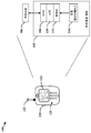
도 1 은 복수의 이용가능한 표준들 중 하나에 따라 선택적으로 동작하는, IC 디바이스들 사이에 데이터 링크를 채용하는 장치를 나타낸다.
도 2 는 베이스밴드 프로세서 및 이미지 센서를 가지고, 이미지 데이터 버스 및 다중-모드 제어 데이터 버스를 구현하는 디바이스를 나타낸다.
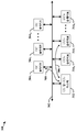
도 3 은 공존하는 I2C 모드 디바이스들 및 CCIe 모드 디바이스들을 지원하는 다목적 또는 공통 직렬 버스를 나타낸다.
도 4 는 IC 디바이스들 사이에 데이터 링크를 채용하는 장치에 대한 시스템 아키텍처 (architecture) 를 나타낸다.
도 5 는 본 명세서에 개시된 특정 양태들에 따른 송신기 및 수신기의 특정 양태들을 나타낸다.
도 6 은 심볼들의 스트림에서의 최하위 심볼이 먼저 송신될 때 2진 비트들을 3진수들로 변환하도록 구성된 로직을 나타낸다.
도 7 은 심볼들의 스트림에서의 최상위 심볼이 먼저 송신될 때 2진 비트들을 3진수들로 변환하도록 구성된 로직을 나타낸다.
도 8 은 12 디지트 3진수를 복수의 비트들로 변환하기 위해 사용될 수도 있는 회로의 일 예를 나타낸다.
도 9 는 본 명세서에서 개시된 특정 양태들에 따라 데이터를 트랜스코딩하기 위한 인코딩 방식을 나타낸다.
도 10 은 레거시 I2C 프로토콜의 전형적인 I2C 비트 전송 사이클을 나타낸다.
도 11 은 종래의 I2C 버스 상에서 SDA 및 SCL 신호 사이의 관계를 나타낸다.
도 12 는 버스에 연결된 디바이스들이 I2C 디바이스를 포함할 때 공유된 버스 상에서 CCIe 모드에서의 데이터 송신의 일 예를 나타낸다.
도 13 은 버스 (430) 상의 디바이스들이 활성 I2C 디바이스를 포함하지 않을 때 CCIe 버스 상에서의 데이터 송신을 나타낸다.
도 14 는 CCIe 동작 모드를 위해 구성되는 직렬 버스 상에서의 송신을 위한 심볼들의 생성을 나타낸다.
도 15 는 I2C 1 바이트 데이터 기록 동작을 나타낸다.
도 16 은 레거시 I2C 슬레이브 모드 상의 START 조건의 효과의 하나의 예를 나타낸다.
도 17 은 동일 직렬 버스 상에서 다중 모드들에서 통신할 수 있는 복수의 디바이스들을 포함하는 시스템을 나타낸다.
도 18 은 레거시 I2C 타이밍 및 시그널링을 또한 지원하는 공유된 직렬 버스 상에서 동작할 수 있는 CCIe 프로토콜의 일 예와 연관된 특정 타이밍 및 시그널링 양태들을 나타낸다.
도 19 는 CCIe 신호가 I2C Fm+ 모드를 위해 사용되는 동일한 물리적 드라이버에 의해 구동될 때 Fm+ 가능 I2C 버스 상에서의 CCIe 심볼 타이밍의 하나의 예를 나타낸다.
도 20 은 I2C 호환 버스에 커플링된 CCIe 디바이스들에 의해 이용될 수도 있는 오픈-드레인 드라이버들의 일 예를 나타낸다.
도 21 은 본 명세서에서 개시된 특정 양태들에 따라 적응될 수도 있는 프로세싱 시스템을 채용하는 장치의 일 예를 나타내는 블록도이다.
도 22 는 본 명세서에서 개시된 하나 이상의 양태들에 따라 CCIe 버스 상에서 정보를 송신하는 방법의 흐름도이다.
도 23 은 본 명세서에서 개시된 하나 이상의 양태들에 따라 CCIe 버스 상에서 정보를 통신하는 송신 장치에 대한 하드웨어 구현의 일 예를 나타내는 도이다.
도 24 는 본 명세서에서 개시된 하나 이상의 양태들에 따라 CCIe 버스로부터 정보를 수신하는 방법의 흐름도이다.
도 25 는 본 명세서에서 개시된 하나 이상의 양태들에 따라 CCIe 버스 상에서 송신되는 정보를 디코딩하는 수신 장치에 대한 하드웨어 구현의 일 예를 나타내는 도이다.
도 26 은 본 명세서에서 개시된 하나 이상의 양태들에 따른 버스를 채용하는 시스템 또는 디바이스를 동작시키는 방법의 흐름도이다.Figure 1 shows an apparatus employing a data link between IC devices, which selectively operates according to one of a plurality of available standards.
Figure 2 shows a device having a baseband processor and an image sensor and implementing an image data bus and a multi-mode control data bus.
Figure 3 shows a multipurpose or common serial bus supporting coexisting I2C mode devices and CCIe mode devices.
Figure 4 shows a system architecture for a device employing a data link between IC devices.
5 illustrates certain aspects of a transmitter and a receiver in accordance with certain aspects disclosed herein.
6 shows logic configured to convert binary bits to triples when the lowest symbol in the stream of symbols is transmitted first.
FIG. 7 shows logic configured to convert binary bits to triples when the most significant symbol in the stream of symbols is transmitted first.
Figure 8 shows an example of a circuit that may be used to convert a 12-digit ternary number to a plurality of bits.
9 illustrates an encoding scheme for transcoding data in accordance with certain aspects disclosed herein.
Figure 10 shows a typical I2C bit transmission cycle for the legacy I2C protocol.
Figure 11 shows the relationship between SDA and SCL signals on a conventional I2C bus.
12 shows an example of data transmission in CCIe mode on a shared bus when the devices connected to the bus include an I2C device.
13 shows data transmission on the CCIe bus when the devices on
Figure 14 shows the generation of symbols for transmission on the serial bus configured for the CCIe mode of operation.
15 shows an I2C 1-byte data write operation.
Figure 16 shows an example of the effect of the START condition on the legacy I2C slave mode.
17 shows a system including a plurality of devices capable of communicating in multiple modes on the same serial bus.
Figure 18 shows specific timing and signaling aspects associated with an example of a CCIe protocol that may operate on a shared serial bus that also supports legacy I2C timing and signaling.
Figure 19 shows an example of CCIe symbol timing on the Fm + capable I2C bus when the CCIe signal is driven by the same physical driver used for the I2C Fm + mode.
Figure 20 shows an example of open-drain drivers that may be used by CCIe devices coupled to an I < 2 > C-compatible bus.
21 is a block diagram illustrating an example of an apparatus employing a processing system that may be adapted in accordance with certain aspects disclosed herein.
22 is a flow diagram of a method for transmitting information on a CCIe bus in accordance with one or more aspects disclosed herein.
23 is an illustration of an example of a hardware implementation for a transmitting device that communicates information on a CCIe bus in accordance with one or more aspects disclosed herein.
24 is a flow diagram of a method for receiving information from a CCIe bus in accordance with one or more aspects disclosed herein.
25 is a diagram illustrating an example of a hardware implementation for a receiving device that decodes information transmitted on a CCIe bus in accordance with one or more aspects disclosed herein.
26 is a flow diagram of a method or system for operating a system employing a bus in accordance with one or more aspects disclosed herein.
이제, 도면들을 참조하여 여러 양태들이 설명된다. 다음의 설명에서, 설명의 목적으로, 하나 이상의 양태들의 완전한 이해를 제공하기 위해 다양한 특정한 세부사항들이 제시된다. 그러나, 이러한 양태(들)은 이러한 특정한 세부사항들이 없이 구현될 수도 있음이 자명할 수도 있다.Various aspects are now described with reference to the drawings. In the following description, for purposes of explanation, numerous specific details are set forth in order to provide a thorough understanding of one or more aspects. It may be evident, however, that such aspect (s) may be implemented without these specific details.
본 출원에서 이용된 바와 같이, 용어들 "컴포넌트", "모듈", "시스템" 등은, 이에 제한되지는 않으나, 하드웨어, 펌웨어, 하드웨어와 펌웨어의 조합, 소프트웨어, 실행 중인 소프트웨어와 같은 컴퓨터 관련 엔티티를 포함하고자 한다. 예를 들면, 컴포넌트는 프로세서 상에서 작동하는 프로세스, 프로세서, 오브젝트, 실행가능물, 실행 스레드, 프로그램, 및/또는 컴퓨터일 수도 있지만, 이들에 제한되는 것은 아니다. 예로서, 컴퓨팅 디바이스 상에서 작동하는 애플리케이션 및 컴퓨팅 디바이스 양자는 컴포넌트일 수 있다. 하나 이상의 컴포넌트들은 프로세스 및/또는 실행의 스레드 내에 상주할 수도 있고, 컴포넌트는 하나의 컴퓨터 및/또는 두 개 이상의 컴퓨터들 사이에 분산되어 로컬라이징될 수도 있다. 또한, 이들 컴포넌트들은 여러 데이터 구조들이 저장된 여러 컴퓨터 판독 가능한 매체로부터 실행될 수도 있다. 컴포넌트들은 하나 이상의 데이터 패킷들 (예를 들면, 로컬 시스템의 다른 컴포넌트, 분산 시스템 및/또는 인터넷과 같은 네트워크를 통해 신호를 통해 다른 시스템들과 상호작용하는 하나의 컴포넌트로부터의 데이터) 을 구비하는 신호에 따르는 것과 같이 로컬 및/또는 원격 프로세스들을 통해 통신할 수도 있다.As used in this application, the terms "component," "module," "system," and the like, include but are not limited to hardware, firmware, a combination of hardware and firmware, software, . For example, a component may be, but is not limited to, a process, processor, object, executable, execution thread, program, and / or computer operating on a processor. By way of example, both an application and a computing device that operate on a computing device may be a component. One or more components may reside within a process and / or thread of execution, and a component may be localized and distributed among one and / or two or more computers. These components may also be executed from various computer readable media having various data structures stored thereon. The components may include signals (e.g., data from one component that interacts with other systems via signals via a network, such as another component of the local system, a distributed system, and / or the Internet) Lt; RTI ID = 0.0 > and / or < / RTI >
또한, 용어 "또는" 은 배제하는 "또는" 이라기 보다는 포함하는 "또는" 을 의미하고자 한다. 즉, 달리 명시되지 않는 한, 또는 문맥에서 명확하지 않는 한, 구문 "X 는 A 또는 B 를 사용한다" 는 자연적으로 포함하는 순열들 중 임의의 것을 의미하고자 한다. 즉, 구문 "X 는 A 또는 B 를 사용한다" 는 다음의 예시들 중 임의의 예시에 의해 만족된다: X 는 A 를 사용한다; X 는 B 를 사용한다; 또는 X 는 A 와 B 양자 모두를 사용한다. 또한, 본 출원 및 첨부된 청구항들에서 이용된 바와 같은 관사 "하나 (a)" 및 "한 (an)" 은 일반적으로, 단수 형태인 것으로 특정되거나 문맥에서 명확하지 않는 한 "하나 이상" 을 의미하는 것으로 해석되어야 한다.Also, the word "or" does not "or" comprises " That is, any of the naturally occurring permutations of the phrase "X uses A or B ", unless otherwise specified or clear in context. That is, the phrase "X uses A or B" is satisfied by any of the following examples: X uses A; X uses B; Or X uses both A and B. It should also be understood that the articles "a" and "an" as used in this application and the appended claims generally mean "one or more" unless the context clearly dictates that it be in the singular Should be interpreted as
본 발명의 특정 양태들은 전자 컴포넌트들 간에 배치된 통신 링크들에 적용가능할 수도 있으며, 이 전자 컴포넌트는 디바이스의 서브컴포넌트들, 이를 테면, 전화기, 모바일 컴퓨팅 디바이스들, 가전 제품들, 오토모바일 전자기기들, 항공 전자기기들 등을 포함할 수도 있다. 도 1 은 IC 디바이스들 사이의 통신 링크를 채택할 수도 있는 장치를 나타낸다. 일 예에서, 장치 (100) 는 무선 액세스 네트워크 (RAN), 코어 액세스 네트워크, 인터넷 및/또는 다른 네트워크와 RF 트랜시버를 통하여 통신하는 무선 통신 디바이스를 포함할 수도 있다. 장치 (100) 는 프로세싱 회로 (102) 에 동작가능하게 커플링되는 통신 트랜시버 (106) 를 포함할 수도 있다. 프로세싱 회로 (102) 는 하나 이상의 IC 디바이스들, 이를 테면, 응용 주문형 IC (ASIC)(108) 를 가질 수도 있다. ASIC (108) 은 하나 이상의 프로세싱 디바이스들, 논리 회로들 등을 포함할 수도 있다. 프로세싱 회로 (102) 는 프로세싱 회로 (102) 에 의해 실행가능할 수도 있는 명령들 및 데이터를 유지할 수도 있는 프로세서 판독가능 저장부, 이를 테면 메모리 (112) 를 포함 및/또는 커플링될 수도 있다. 프로세싱 회로 (102) 는 무선 디바이스의 저장부 (112) 내에 상주하는 소프트웨어 모듈의 실행을 가능하게 하고 지원하는 애플리케이션 프로그래밍 인터페이스 (API)(110) 계층 및 오퍼레이팅 시스템 중 하나 이상에 의해 제어될 수도 있다. 메모리 디바이스 (112) 는 ROM (read-only memory) 또는 RAM (random-access memory), EEPROM (electrically erasable programmable read-only memory), 플래시 카드들, 또는 프로세싱 시스템 및 컴퓨팅 플랫폼들에 이용될 수 있는 임의의 메모리 디바이스를 포함할 수도 있다. 프로세싱 회로 (102) 는 장치 (100) 를 구성하고 동작시키는데 사용된 동작 파라미터들 및 다른 정보를 유지할 수 있는 로컬 데이터베이스 (114) 를 포함하거나 로컬 데이터베이스 (114) 에 액세스할 수도 있다. 로컬 데이터베이스 (114) 는 데이터베이스 모듈, 플래시 메모리, 자기 매체, EEPROM, 광학 매체, 테이프, 소프트 또는 하드 디스크, 등등 중 하나 이상을 사용하여 구현될 수도 있다. 프로세싱 회로는 또한, 다른 컴포넌트들 중에서 안테나 (122), 디스플레이 (124), 오퍼레이터 제어부들, 예컨대 버튼 (128) 및 키패드 (126) 와 같은 외부 디바이스들에 동작가능하게 커플링될 수도 있다.Certain aspects of the invention may be applicable to communication links disposed between electronic components, which may be subcomponents of a device, such as a telephone, mobile computing devices, home appliances, , Avionics, and the like. 1 illustrates an apparatus that may employ a communication link between IC devices. In one example, the
I2C 및 CCIe 동작들 양자를 지원하는 버스 아키텍처의 예Example of a bus architecture that supports both I2C and CCIe operations
도 2 는 베이스밴드 프로세서 (204) 및 이미지 센서 (206) 를 갖는 디바이스 (202) 의 단순화된 예를 나타내는 블록도 (200) 이다. 이미지 데이터 (216) 및 다중-모드 제어 데이터 버스 (208) 가 디바이스 (202) 에서 구현될 수도 있다. 도 (200) 는 카메라 디바이스 (202) 를 오직 예시적인 방식으로 나타내고, 제어 데이터 버스 (208) 를 이용하여 다양한 다른 디바이스들 및/또는 상이한 기능들이 구현, 동작 및/또는 통신할 수도 있다. 묘사된 예에서, 이미지 데이터는 MIPI 에 의해 정의된 "DPHY" 고속 차동 링크와 같은 이미지 데이터 버스 (216) 를 통해 이미지 센서 (206) 로부터 베이스밴드 프로세서 (204) 로 전송될 수도 있다. 하나의 예에서, 제어 데이터 버스 (208) 는 I2C 버스 모드에서의 동작을 위해 구성가능한 2 개의 선들을 가질 수도 있다. 따라서, 제어 데이터 버스 (208) 는 SCL 및 SDA 선들을 포함할 수도 있다. SCL 은 I2C 프로토콜들에 따라 제어 데이터 버스 (208) 를 통한 데이터 전송들을 동기화하기 위해 시용될 수도 있는 클럭 신호를 반송할 수도 있다. 데이터 라인 SDA 및 클럭 라인 SCL 은 I2C 버스 (제어 데이터 버스 (208)) 상에서 다수의 디바이스들 (212, 214, 및 218) 에 커플링될 수도 있다. 이 예에서, 제어 데이터는 제어 데이터 버스 (208) 를 통해 베이스밴드 프로세서 (204) 와 이미지 센서 (206) 및 다른 주변 디바이스들 (218) 사이에서 교환될 수도 있다. I2C 프로토콜들에 따르면, SCL 선 상의 클럭 속도들은 보통의 I2C 동작에 대해 100KHz 까지, I2C 고속 모드에 대해 400KHz 까지, 그리고 I2C 고속 모드 플러스 (Fm+) 에 대해 1MHz 까지일 수도 있다. I2C 버스를 통한 이들 동작 모드들은 카메라 애플리케이션들에 대해 이용될 때 카메라 제어 인터페이스 (CCI) 로서 지칭될 수도 있다.Figure 2 is a block diagram 200 illustrating a simplified example of a
하나의 양태에 따르면, 향상된 동작 모드는 카메라 동작을 지원하기 위해 다중-모드 제어 데이터 버스 (208) 를 통해 구현될 수도 있다. 향상된 동작 모드는 데이터가 1MHz 보다 더 큰 레이트 (rate) 에서 전송될 수 있게 할 수도 있고, 향상된 모드는 CCI 확장 (CCIe) 모드로서 지칭될 수도 있다.According to one aspect, the enhanced mode of operation may be implemented via a multi-mode
하나의 예에서, CCIe 버스는 CCIe 버스 동작들과 호환가능한 디바이스들에 대해 보다 높은 데이터 레이트들을 제공하기 위해 사용될 수도 있다. 이러한 디바이스들은 CCIe 디바이스들로서 지칭될 수도 있고, CCIe 디바이스들은 종래의 CCI 버스의 SCL 라인 및 SDA 라인 양자를 이용하여 송신되는 심볼들로서 데이터를 인코딩함으로써 서로 통신할 때 더 높은 데이터 레이트들을 획득할 수 있다. CCIe 는 카메라 애플리케이션들에 대해 이용될 수도 있다. CCIe 디바이스들 및 I2C 디바이스들은 동일 CCIe 버스 상에서 공존할 수도 있어, 제 1 시간 간격에서, 데이터는 CCIe 인코딩을 이용하여 송신될 수도 있고, 다른 데이터는 I2C 시그널링 규약들 및 프로토콜들에 따라 상이한 시간 간격에서 송신될 수도 있다.In one example, the CCIe bus may be used to provide higher data rates for devices compatible with CCIe bus operations. Such devices may be referred to as CCIe devices and CCIe devices may obtain higher data rates when communicating with each other by encoding data as symbols to be transmitted using both the SCL line and SDA line of a conventional CCI bus. CCIe may also be used for camera applications. The CCIe devices and the I2C devices may coexist on the same CCIe bus such that in a first time interval the data may be transmitted using CCIe encoding and other data may be transmitted at different time intervals according to I2C signaling protocols and protocols May be transmitted.
디바이스 (202) 가 CCIe 모드를 위해 구성될 때, 베이스밴드 프로세서 (204) 는 마스터 노드 (212) 를 포함하고, 이미지 센서 (206) 는 슬레이브 노드 (214) 를 포함하며, 양 마스터 노드 (212) 및 슬레이브 노드 (214) 는 제어 데이터 버스 (208) 에 커플링된 임의의 레거시 I2C 디바이스들의 적절한 동작에 영향을 미침이 없이 제어 데이터 버스 (208) 를 통해 CCIe 모드 프로토콜들에 따라 동작한다. 제어 데이터 버스 (208) 는 CCIe 디바이스들과 레거시 I2C 슬레이브 디바이스들 사이에 브릿지 디바이스 없이 CCIe 모드 동작들을 지원할 수도 있다.When the
하나의 예에서, 제어 데이터 버스 (208) 상에서의 제 1 교환 동안, 레거시 I2C 디바이스들은 제 1 클럭, 제 1 버스 속도, 및/또는 제 1 신호 프로토콜을 갖는 제 1 모드에서 동작할 수도 있는 한편, 제어 데이터 버스 (208) 상에서의 제 2 교환 동안 CCIe-가능 디바이스들은 제 2 클럭, 제 2 버스 속도, 및/또는 제 2 프로토콜을 갖는 제 2 모드에서 동작할 수도 있다. 제 1 클럭, 제 1 버스 속도, 및/또는 제 1 신호 프로토콜은 제 2 클럭, 제 2 버스 속도, 및/또는 제 2 프로토콜과 구분될 수도 있다. 예를 들어, 제 2 클럭 및/또는 제 2 버스 속도는 제 1 클럭 및/또는 제 1 버스 속도보다 각각 더 빠를 수도 있거나 더 큰 속도를 가질 수도 있다.In one example, during a first exchange on the
다른 예에서, 모든 슬레이브 디바이스들 (218) 은 제 1 동작 모드와 제 2 동작 모드 사이에서 스위칭할 필요가 없도록 CCIe-가능 디바이스들일 수도 있다. 즉, 모든 시그널링 및/또는 통신은 제 2 클럭 및/또는 제 2 버스 속도를 이용하고 제 2 프로토콜을 이용하는 제 2 모드에 따라 수행될 수도 있다. 모든 슬레이브 디바이스들 (218) 이 CCIe-가능 디바이스들일 때 제 2 모드는 제 1 모드보다 더 큰 비트 레이트를 제공할 수도 있기 때문에 제 1 모드와 제 2 모드 사이에 스위칭할 필요성 또는 이점이 존재하지 않는다. 일부 경우들에서, 제 1 모드가 수용될 필요가 없을 때 제 2 모드보다 훨씬 더 큰 비트 레이트를 제공하지만 I2C 디바이스들과 호환가능하지 않은 제 3 동작 모드가 구현될 수도 있다.In another example, all
도 3 은 공존 I2C 모드 디바이스들 (3041-304m) 및 CCIe 모드 디바이스들 (312, 및 3141-314n) 을 지원하는 공통 버스 (302) 를 나타내는 블록도이다. I2C 모드 트랜잭션들 (transactions) (308) 에 대해, CCIe-가능 마스터 디바이스 (312) 는 1Mbps 의 최대 데이터 레이트를 획득하기 위해 I2C Fm+ 또는 CCI 프로토콜을 이용하여 버스 (302) 상에서 I2C 슬레이브 디바이스들 (3041-304m) 과 통신할 수도 있다. CCIe-가능 마스터 디바이스 (312) 가 완전한 CCI 또는 I2C Fm+ 성능을 지원할 수도 있는 한편, CCIe-가능 슬레이브 디바이스 (3141-314n) 는 완전한 I2C 성능을 지원하도록 요구되지 않는다.3 is a block diagram illustrating a
CCIe-가능 마스터 디바이스 (312) 는 또한 CCIe-가능 슬레이브 디바이스 (3141-314n) 과 CCIe 모드 통신들 (306) 을 확립할 수도 있다. CCIe 모드는 단일 마스터 동작을 허용하고, 다중 마스터들은 지원되지 않는다. CCIe 모드에서, CCIe 마스터 디바이스 (312) 는 제어 데이터 버스 (302) 상에서 오직 CCIe-가능 슬레이브 디바이스들 (3141-314n) 과만 통신한다. CCIe-가능 디바이스들 (312, 및 3141-314n) 은 I2C 모드들에서보다 CCIe 모드에서 상당히 더 높은 데이터 레이트들로 통신할 수도 있다. 예를 들어, CCIe-가능 디바이스들 (312, 및 3141-314n) 은 6.4Mbps, 또는 16.7Mbps 의 데이터 레이트들로 통신할 수도 있다.The CCIe-
디폴트 기동 (start-up) 모드가 버스 (302) 에 대해 구성 또는 정의될 수도 있다. 하나의 예에서, 버스 (302) 는 전원 켜짐, 리셋 및/또는 다른 유형의 기동 조건 후에 CCIe 동작 모드에서 동작하도록 구성될 수도 있다. 다른 예에서, 버스 (302) 는 초기에 레거시 I2C 모드에서 동작하도록 구성될 수도 있다. CCIe-가능 마스터 디바이스 (312) 는, 예컨대 CCIe-가능 슬레이브 디바이스들 (3141-314n) 에 대한 액세스 (access) 가 소망될 때 송신되는 I2C 일반 콜 (call) 을 통해 버스 (302) 의 동작 모드가 I2C 모드로부터 CCIe 모드로 스위칭하게 할 수도 있다. CCIe-가능 마스터 디바이스 (312) 는, 버스 (302) 상에서 I2C 슬레이브 디바이스들 (3041-304m) 을 액세스하기 위해 CCIe "엑시트 (exit)" 프로토콜 및 I2C 일반 콜의 결합을 통해 CCIe 모드로부터 I2C 모드로 스위칭할 수도 있다.A default start-up mode may be configured or defined for the
CCIe 동작들을 위해 적응되는 디바이스의 특정 양태들을 나타내는 예Example showing specific aspects of the device adapted for CCIe operations
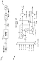
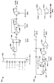
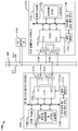
도 4 는 CCIe 버스 (430) 와 같은 통신 버스를 채용할 수도 있는 장치 (400) 의 특정 양태들을 나타내는 블록 모식도이다. 장치 (400) 는 무선 모바일 디바이스, 모바일 텔레폰, 모바일 컴퓨팅 시스템, 무선 텔레폰, 노트북 컴퓨터, 태블릿 컴퓨팅 디바이스, 미디어 플레이어, 게이밍 디바이스 등 중 하나 이상에서 구현될 수도 있다. 장치 (400) 는 CCIe 버스 (430) 를 이용하여 통신하는 다수의 디바이스들 (402, 420, 및/또는 422a-422n) 을 포함할 수도 있다. CCIe 버스 (430) 는, CCIe 버스 (430) 에 의해 지원되는 개선된 특징들을 위해 구성되는 디바이스들에 대해 종래의 CCI 버스의 성능들을 확장할 수 있다. 예를 들어, CCIe 버스 (430) 는 CCI 버스보다 더 높은 비트 레이트를 지원할 수도 있다. 본 명세서에서 개시된 특정 양태들에 따르면, CCIe 버스 (430) 의 일부 버전들 (versions) 은 16.7Mbps 이상의 비트 레이트들을 지원하도록 구성 또는 적응될 수도 있고, CCIe 버스의 일부 버전들은 적어도 초당 23 메가비트들의 데이터 레이트들을 지원하도록 구성 또는 적응될 수도 있다.4 is a block diagram illustrating certain aspects of a
도 4 에서 도시된 예에서, 이미징 (imaging) 디바이스 (402) 는 CCIe 버스 (430) 상에서 슬레이브 디바이스로서 동작하도록 구성된다. 이미징 디바이스 (402) 는 예를 들어 이미지 센서를 관리하는 센서 제어 기능부 (404) 를 제공한다. 또한, 이미징 디바이스 (402) 는 구성 레지스터들 (configuration registers) (406) 및/또는 다른 스토리지 (storage) 디바이스 (402), 프로세싱 회로 및/또는 제어 로직 (412), 트랜시버 (410) 및 라인 드라이버들/수신기들 (414a 및 414b) 을 포함할 수도 있다. 프로세싱 회로 및/또는 제어 로직 (412) 은 상태 머신, 시퀀서, 신호 프로세서 또는 범용 프로세서와 같은 프로세서를 포함할 수도 있다. 트랜시버 (410) 는, 타이밍, 로직 및 스토리지 회로들 및/또는 디바이스들을 포함하는, 수신기 (410a), 송신기 (410c) 및 소정의 공통 회로들 (410b) 을 포함할 수도 있다. 일부 경우들에서, 트랜시버 (410) 는 인코더들 및 디코더들, 클럭 및 데이터 복원 회로들 등을 포함할 수도 있다.In the example shown in FIG. 4, the
송신 클럭 (TXCLK) 신호 (428) 가 송신기 (410c) 에 제공될 수도 있고, 여기서, TXCLK 신호 (428) 는 CCIe 통신 모드를 위한 데이터 송신 레이트들을 결정하기 위해 사용될 수도 있다. SDA 선 (418) 및 SCL 선 (416) 이 송신된 데이터를 인코딩하기 위해 사용될 때, TXCLK 신호 (428) 는 CCIe 버스 (430) 상에서 송신되는 심볼들의 시퀀스들 내에 임베딩될 (embedded) 수도 있다. 하나의 예에서, TXCLK 신호 (428) 는 천이 클럭 트랜스코딩을 이용하여 임베딩될 수도 있고, 이에 의해, 물리적 링크 (430) 를 통해 송신될 데이터는, 적어도 하나의 선 (416 및/또는 418) 의 상태의 변화가 CCIe 버스 (430) 상에서 송신되는 연속적인 심볼들의 각 쌍 사이에서 발생하도록 트랜스코딩된다.A transmit clock (TXCLK) signal 428 may be provided to the
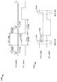
도 5 는 본 명세서에서 개시된 특정 양태들에 따라 구성된 송신기 (500) 및 수신기 (520) 의 일 예를 나타내는 블록도이다. CCIe 동작들에 대해, 송신기 (500) 는 데이터 (510) 를, SCL (416) 및 SDA (418) 신호 선들 상에서 송신되는 심볼들로서 인코딩되는 3진 (베이스-3) 천이 넘버들로 트랜스코딩할 수도 있다. 묘사된 예에서, 입력 데이터 (510) 의 각 데이터 엘리먼트 (또한 데이터 워드로서도 지칭됨) 는 19 또는 20 비트들을 가질 수도 있다. 컨버터 및/또는 트랜스코더 (502) 는 입력 데이터 (510) 를 수신할 수도 있고, 각 데이터 엘리먼트에 대해 3진 천이 넘버를 생성할 수도 있다. 각 3진 천이 넘버는 12 개의 3진 디지트들의 시퀀스 (512) 로서 제공될 수도 있고, 각 3진 디지트는 2 개의 비트들에 의해 표현된다. 인코더 (504) 는 12 3진 디지트들의 시퀀스 (512) 를 수신하고, 라인 드라이버들 (line drivers) (506) 을 통해 송신되는 2-비트 심볼들 (514) 의 스트림을 생성한다. 묘사된 예에서, 라인 드라이버들 (506) 은 오픈-드레인 출력 트랜지스터들 (508) 을 포함한다. 하지만, 다른 예들에서, 라인 드라이버들 (506) 은 푸시-풀 (push-pull) 드라이버들을 이용하여 SCL (416) 및 SDA (418) 신호 선들을 구동할 수도 있다. 인코더 (504) 에 의해 생성되는 2-비트 심볼들 (514) 의 출력 스트림은, 연속적인 심볼들의 어느 쌍도 2 개의 동일한 심볼들을 포함하지 않는 것을 보장함으로써 연속적인 심볼들 (514) 사이에 SCL (416) 및 SDA (418) 신호 선들의 적어도 하나의 상태에서의 천이를 갖는다. 적어도 하나의 선 (416 및/또는 418) 에서의 상태의 천이의 이용가능성은, 수신 회로 (520) 가 심볼들의 스트린 (536) 의 수신된 버전으로부터 클럭 정보를 추출하고 데이터 심볼들의 스트린 (536) 으로부터 수신 클럭 (538) 을 도출하는 것을 허용한다.5 is a block diagram illustrating an example of a
CCIe 시스템에서, 수신기 (520) 는 클럭 및 데이터 복원 (clock and data recovery; CDR) 회로 (528) 를 포함하거나 그것과 협동할 수도 있다. 수신기 (520) 는 CDR 회로 (528) 에 로 (raw) 2-비트 심볼들 (536) 의 스트림을 제공하는 인터페이스 회로들 (526) 을 포함할 수도 있다. CDR 회로 (528) 는 로 심볼들 (536) 로부터 수신 클럭 (538) 을 추출하고, 2-비트 심볼들의 스트림 (534) 및 수신 클럭 (538) 을 수신기 (520) 의 다른 회로들 (524 및 522) 에 제공한다. 몇몇 예들에서, CDR 회로 (528) 는 다수의 클럭들 (538) 을 생성할 수도 있다. 하나의 예에서, CDR 회로 (528) 는 SCL 신호 선 (416) 상에서 및/또는 SDA 신호 선 (418) 상에서 천이들을 검출하고 이러한 검출 시에 수신 클럭 (538) 의 상태를 토글링하는 로직을 포함한다. CDR 회로 (528) 는, 동일한 심볼 경계에서 SCL 신호 선 (416) 및 SDA 신호 선 (418) 상에서의 천이들이 서로에 대해 지연될 때, 수신 클럭 (538) 의 상태의 다중 토글들 (toggles) 을 배제하기 위해, 원-샷들, 지연 회로들 또는 다른 이러한 엘리먼트들과 같은 시간-감지 회로를 포함할 수도 있다. 디코더 (524) 는 심볼들의 스트림 (534) 을 12 개의 3진 디지트들의 시퀀스들 (532) 로 디코딩하기 위해 수신 클럭 (538) 을 이용할 수도 있고, 각 시퀀스 (532) 는 천이 넘버를 나타낸다. 12-디지트 천이 넘버 (532) 의 각 디지트는 2-비트 3진 디지트로서 표현될 수도 있다. 트랜스코더 및/또는 컨버터 (522) 는 그 다음, 12 개의 3진 디지트들의 각 시퀀스 (532) 을 19-비트 또는 20-비트 출력 데이터 엘리먼트들 (530) 로 변환할 수도 있다.In the CCIe system, the
특정 양태들에 따르면, 천이 넘버를 나타내는 입력 2진 데이터 (510) 와 3진 디지트들의 시퀀스 (512) 사이의 및/또는 천이 넘버들 (532) 과 출력 데이터 비트들 (530) 사이의 변환들은 컨버터들 (502 및 522) 에 의해 수행된다. 하나의 예에서, 송신기 (500) 에서의 데이터 비트들 (510) 로부터 천이 넘버들로의 그 다음에 수신기 (520) 에서의 천이 넘버들로부터 데이터 비트들 (530) 로의 변환은 2-선 인터페이스 (430) 에 대해 12 개의 천이 심볼들을 수반한다. 셋트 또는 시퀀스 {T11, T10, ..., T2, T1, T0} 에서 각 천이 넘버 T 에 대한 결과적인 r 개의 가능한 심볼 천이 상태들은 12 개의 천이 넘버들에 대해 총 r12 개의 상이한 상태들을 제공한다. 2-선 버스에 대해, 각 시그널링 상태로부터 이용가능한 천이 상태들의 수 r = 22-1 이다. 결과적으로, 천이들의 시퀀스 {T11, T10, ..., T2, T1, T0} 는 (22-1)12 = 312 = 531441 의 상이한 상태들을 갖는 데이터를 인코딩할 수 있다. 이 후자의 예에서, 12-디지트 3진수 {T11, T10, ..., T2, T1, T0} 에서의 각 천이 Ti 는 {0, 1, 2} 로부터 선택된다.Transitions between input
예를 들어, {T11, T10, ..., T2, T1, T0} = {2, 1, 0, 0, 1, 1, 0, 1,0, 1, 2, 1} 에 대해, 12-천이 시퀀스들을 나타내는 3진수는:For example, for {T11, T10, ..., T2, T1, T0} = {2,1,0,0,1,1,0,0,0,1,1,2,1} The trinary numbers representing the transition sequences are:
2100_1101_01213 (3진수)2100_1101_0121 3 (3 digits)
= 2×311+1×310+0×39+0×38 = 2 x 3 11 + 1 x 3 10 + 0 x 3 9 + 0 x 3 8
+ 1×37 +1×36 +0×35+1×34 + 1 x 3 7 + 1 x 3 6 + 0 x 3 5 + 1 x 3 4
+ 0×33 +1×32 +2×31+1×30 + 0 x 3 3 + 1 x 3 2 + 2 x 3 1 + 1 x 3 0
= 416356 (0x65A64) 이다.= 416356 (0x65A64).
이러한 방식으로, 천이 넘버의 12 개의 3진 디지트들은 20-비트 데이터 출력 (530) 으로 변환될 수도 있다.In this manner, twelve ternary digits of the transition number may be converted to a 20-bit data output 530. [
도 5 에서 도시된 2-선 시스템의 예에서, 12 심볼 천이 넘버들은 n-선 시스템 및 m 심볼 천이 넘버들로서 일반화될 수도 있다. 셋트 또는 시퀀스 {T m -1, ..., T1, T0} 에서 각각의 천이 넘버 T 에 대해 r 개의 가능한 심볼 천이 상태들이 존재할 때, m 천이 시퀀스는 rm 개의 상이한 상태들을 인코딩할 수 있고, 여기서, r = 2 n -1 이다. 결과적으로, 시퀀스 {T m -1, ..., T1, T0} 는 (2 n -1) m 개까지의 상이한 상태들을 갖는 데이터를 인코딩할 수도 있다.In the example of the two-wire system shown in Figure 5, the twelve symbol transition numbers may be generalized as an n-ray system and m symbol transition numbers. When there are r possible symbol transition states for each transition number T in a set or sequence {T m -1 , ..., T 1 , T 0 }, the m transition sequence can encode rm different states , Where r = 2 n -1. As a result, the sequence {T m -1 , ..., T 1 , T 0 } may encode data having up to (2 n -1) m different states.
하나의 예에서, 2-선, 12-심볼 인터페이스에서 심볼 천이 넘버 (532) 를 나타내는 3진수는 다음과 같이 2진수 출력 데이터 비트들 (bits) (530) 로 변환될 수 있다:In one example, a ternary number representing the

송신기 (500) 에서, 2-선, 12-심볼 인터페이스에서 SCL 선 (416) 및 SDA 선 (418) 상에서의 송신을 위한 심볼들 (514) 로서 인코딩될 수도 있는 3진수 (512) 로 데이터 비트들 (510) 을 변환하는 알고리즘. 이 알고리즘은 내림차순으로 천이 넘버 (Ti) 값들을 그들의 대응하는 나머지 (Mi) 로 반복적으로 계산할 수도 있다. 즉, 다음과 같이 각 디지트는 상위 디지트 계산에서 사용된 모듈로 (modulo) 연산의 나머지를 디지트 넘버의 승수 (power) 로 나누고, 소수점 수들은 폐기함으로써 계산될 수 있다:At

후자의 알고리즘은 다음으로부터 합성될 수도 있다:The latter algorithm may be synthesized from the following:

도 6 은 심볼들의 스트림에서의 최하위 심볼이 먼저 송신될 때 2진 입력 데이터 비트들 (510) 을 3진 천이 넘버들 (512) 로 변환하기 위한 예시적인 로직 (620 및 640) 을 나타낸다. 로직 (620, 640) 은 컨버터 (502) 에서 구현될 수도 있다. 단순화된 블록도 (600) 로 나타낸 바와 같이, 컨버터 (520) 에 의해 생성된 각각의 3진 천이 넘버 (512) 는 입력 데이터 비트들 (510) 에서의 다수의 비트들로부터 도출될 수도 있고, 각 3진 천이 넘버 (512) 는 12 디지트들 (T0, T1...T11) (602) 을 포함할 수도 있다. 3진수들 (512) 은 그 후에 수신 디바이스 (520) 에 송신되는 심볼들 (514) 로 트랜스코딩된다. 12 디지트 3진 천이 넘버에 대해, 그 수를 나타내는 T0, T1...T11 에 있어서, T0 는 30 디지트를 나타내고 최하위 디지트인 반면, T11 은 311 디지트를 나타내고 최상위 디지트이다. 도 5 와 관련하여 논의된 바와 같이, 이들 3진 천이 넘버들 (512) 클럭과 함께 임베딩되고, 수신 디바이스 (520) 에 송신되는 순차적인 심볼들 (514) 로 인코딩된다. 로직 다이어그램 (620) 및 로직 회로 (640) 는 입력 데이터 비트들 (510) 을 "최하위 심볼 우선 (least significant symbol first)" 3진 천이 넘버들 (512) 의 스트림으로 변환한다.Figure 6 shows
도 7 은, 심볼들의 스트림에서 최상위 심볼이 먼저 송신될 때 2진 입력 데이터 비트드르 (510) 을 3진 천이 넘버들 (712) 로 변환하기 위한 로직 (720) 을 나타낸다. 로직 (720) 은 컨버터 (704) (도 5 의 컨버터 (502) 와 비교) 에서 구현될 수도 있다. 단순화된 블록도 (700) 로 나타낸 바와 같이, 컨버터 (704) 에 의해 생성된 각각의 3진 천이 넘버 (712) 는 입력 데이터 비트들 (510) 에서의 다수의 비트들로부터 도출될 수도 있고, 각 3진 천이 넘버 (712) 는 12 디지트들 (T0, T1...T11) (702) 을 포함할 수도 있으며, 이에 의해, T0 는 30 디지트를 나타내고 최하위 디지트인 반면, T11 은 311 디지트를 나타내고 최상위 디지트이다. 3진수들 (712) 은 그 후에 수신 디바이스에 송신되는 심볼들로 트랜스코딩된다.FIG. 7 shows
이 예에서, 변환은 T11 로 시작한다. 도 6 은 T0, T1, T2,..., T11 의 순서로 전송되는 12 디지트 3진수 (602) 를 나타내는 반면, 도 7 은 12 디지트 3진수 (702) 가 T11, T10, T9,..., T0 의 순서로 전송되는 일 예에 관한 것이다. 도 6 의 예시적인 로직 (620 및 640) 과 도 7 에서의 회로 (720) 사이에 소정의 차이들이 식별가능하다. 도 6 의 회로 (640) 는 24 개의 플립-플롭들 (flip-flops) 을 포함하고, 멀티플렉서, 20 개의 플립-플롭들, 및 로직 디바이스들을 포함하는 도 7 의 회로 (720) 에 비해 훨씬 복잡하다. 따라서, 최상위 비트가 먼저 전송될 때, 로직 게이트들에서의 감소 때문에, 수반되는 로직 및 회로는 복잡성 면에서 단순화되고 덜 비싸다.In this example, the conversion starts with T 11 . FIG. 6 shows a 12-digit ternary 602 transmitted in the order of T 0 , T 1 , T 2 , ..., T 11 while FIG. 7 shows a 12-digit ternary 702 with T 11 , T 10 , T 9 , ..., T 0 in this order. Certain differences between the
언급된 바와 같이, 도 6 의 로직 (620, 640) 은 최하위 심볼이 수신 디바이스에 먼저 송신되기 때문에 최하위 심볼 우선 (least significant symbol first) (LSS 우선) 로직 및 회로를 나타내는 반면, 도 7 의 로직 (720) 은 최상위 심볼이 수신 디바이스에 먼저 송신되는 (MSS 우선) 예를 나타낸다. 본 명세서에서 사용된 바와 같이 "최하위 심볼 (least significant symbol)" 은 3진수의 최하위 디지트에 대응하는 트랜스코딩된 심볼을 지칭한다. 예를 들어, T0 가 순차적인 심볼로 트랜스코딩될 때, 그 심볼은 그것이 최하위 3진 디지트로부터 유래되기 때문에 최하위 심볼이다. 그리고, 심볼-대-천이 넘버 컨버터 (예컨대, 도 5 의 트랜스코더 (524)) 가 그 후에 그 트랜스코딩된 (순차적인) 심볼을 천이 넘버 (532), 즉 하나의 3진 디지트 넘버로 변환할 때, 그것은 최하위 디지트일 것이다. 유사하게, 본 명세서에서 사용된 바와 같이 "최상위 심볼 (most significant symbol)" 은 3진수의 최상위 디지트에 대응하는 트랜스코딩된 심볼을 지칭한다.As noted, the
도 8 은 12 디지트 3진수를 출력 비트들 (824) 로 변환하기 위해 사용될 수도 있는 회로의 일 예 (800) 를 나타낸다. 본 명세서에서 기술된 바와 같이, 예를 들어 열아홉 (19) 또는 스물 (20) 비트들의 원래 데이터 (510) 는 역순으로 3진 천이 넘버로 변환될 수도 있고, 이에 의해, 최상위 비트는 컨버터에 먼저 공급된다 (도 7 및 설명들 참조). 천이 넘버는 역순으로 다시 순차적인 심볼들로 변환 (즉, 트랜스코딩) 될 수도 있고, 이들 트랜스코딩된 심볼들은 역순으로 버스 상에서 송신된다. 수신 디바이스 (예컨대, 슬레이브 디바이스) 는 역순 송신물을 수신하고, 트랜스코딩된 심볼들을 다시 역으로 3진수로 변환하기 위해 클럭 복원 및 심볼 샘플링을 수행하며, 이 3진수는 그 후에, 3진수를 다시 역으로 20 비트 2진 원래 데이터로 변환하는 회로에 역순으로 공급된다. 회로 (800) 는 로직 디바이스에 대해 단일 출력에 커플링된 12 개의 입력들을 갖는 멀티플렉서 (802) 를 이용할 수도 있다.8 shows an example of a
최상위 심볼 우선 동작 모드와 최하위 심볼 우선 동작 모드 사이의 선택은 카운터 (850) 가 카운트하는 방향에 의해 제어될 수도 있다. 예를 들어, 카운터 (850) 가 16진수 "0xB" (즉, 10진수 "11") 로부터 감분하는 다운 카운터로서 동작하도록 구성 또는 제어될 때, 최상위 심볼들이 먼저 핸들링될 수도 있다. 카운터 (850) 가 16진수 "0x0" (즉, 10진수 "0") 으로부터 증분하는 업 카운터로서 동작하도록 구성 또는 제어되는 경우, 최하위 심볼들이 먼저 핸들링될 수도 있다. 대안적으로 또는 추가적으로, 멀티플렉서 (802) 에 대한 입력들의 순서는, 멀티플렉서 (820) 가 소망된 순서의 출력 3진 천이 넘버들을 생성하기 위해 카운터 (850) 의 출력 (DELCNT) (814) 에 응답하도록 구성될 수도 있다.The selection between the highest symbol priority operation mode and the lowest symbol priority operation mode may be controlled by the direction in which the
카운터 (850) 는, CDR 회로 (528) 의 출력 및/또는 시스템 클럭으로부터 도출될 수도 있는 클럭에 동기화된 레지스터 또는 래치 (860) 를 이용하여 DELCNT (814) 출력을 제공할 수도 있다. 레지스터 (860) 는 카운터 (850) 를 초기화하는 제어 신호 (START 신호) (864) 에 기초하여 다음 값 또는 시작 값 사이에서 선택하는 제 1 멀티플렉서 로직 (858) 으로부터 입력된 4-비트 입력을 수신한다. 시작 값은, 컨버터가 최상위 심볼 우선 모드에서 동작할 때 0xB 로 설정될 수도 있고, 컨버터가 컨버터가 최하위 심볼 우선 모드에서 동작할 때 0x0 으로 설정될 수도 있다. 제 1 멀티플렉서 로직 (858) 은, 종단-검출 로직 (854) 에 의한 종단 조건의 검출에 기초하여 DELCNT (814) 출력의 변형된 버전과 DELCNT (814) 출력 사이에서 선택하는 제 2 멀티플렉서 로직 (856) 으로부터 다음 값을 수신한다. 제 2 멀티플렉서 (856) 의 변형된 입력은, 카운트-다운 연산에 대해 감산 로직에 의해 또는 카운트-업 연산에 대해 가산 로직으로부터 제공될 수도 있는, 함수 (852) 의 결과일 수도 있다. 나타낸 바와 같이, 제 2 멀티플렉서 로직 (856) 은 DELCNT (814) 출력이 0x0 으로부터 0xF 로 감분되어 현재 변환의 종단을 나타낸 후에 DELCNT (814) 출력을 반복한다. 카운트 다운 동작 모드에 대해, 종단-검출 로직 (854a) 은 DELCNT (814) 에 대해 0xF 값을 검출하도록 구성될 수도 있고, 종단-검출 로직 (854a) 은, START 신호 (864) 가 시작 값이 로딩되게끔 할 때까지, DELCNT (814) 가 0xF 에서 유지되게 하도록 제 2 멀티플렉서 로직 (856) 출력을 스위칭한다. 카운트 업 동작에 대해, 종단-검출 로직 (854b) 은 DELCNT (814) 에 대해 0xC (10진수 "12" 또는 2진수 "1100") 값을 검출하도록 구성될 수도 있다.The
CCIe 인코딩의 예Example of CCIe encoding
도 9 는 3진 천이 넘버들 (512) 로부터 심볼들의 시퀀스 (514) 를 생성하기 위해 트랜스코더 (504) 에 의해 이용될 수도 있는 인코딩 방식 (900) 을 나타내는 도면이고, 여기서, 심볼들의 시퀀스 (514) 는 클럭 정보를 임베딩했고, CCIe 버스 (430) 상에서의 송신을 위한 것이다. 인코딩 방식 (900) 은 또한, CCIe 버스 (930) 상에서 송신되는 심볼들 (534) 로부터 3진 천이 넘버들 (532) 을 추출하기 위해 트랜스코더 (524) 에 의해 이용될 수도 있다. CCIe 인코딩 방식 (900) 에서, CCIe 버스 (430) 의 2 개의 선들은 4 개의 기본 심볼들 S: {0, 1, 2, 3} 의 정의를 허용한다. 심볼들의 시퀀스 (514, 534) 에서의 임의의 2 개의 연속적인 심볼들은 상이한 상태들을 가지고, 심볼 시퀀스들 0,0, 1,1, 2,2 및 3,3 은 연속적인 심볼들의 유효하지 않은 조합들이다. 따라서, 오직 3 개의 유효한 심볼 천이들이 각 심볼 경계에서 이용가능하고, 여기서, 심볼 경계는 송신 클럭에 의해 결정되며, 제 1 심볼 (이전 심볼 Ps) (922) 이 종결되고 제 2 심볼 (현재의 심볼 Cs) (924) 이 시작되는 포인트를 나타낸다.9 is a diagram showing an
본 명세서에서 개시된 특정 양태들에 따르면, 3 개의 이용가능한 천이들이 가 Ps 심볼 (922) 에 대해 천이 넘버 (T) (926) 를 할당받는다. T (926) 의 값은 3진수에 의해 표현될 수 있다. 하나의 예에서, 천이 넘버 (926) 의 값은 인코딩 방식에 대해 심볼-오더링 서클 (902) 을 할당함으로써 결정된다. 심볼-오더링 서클 (902) 은 4 개의 가능한 심볼들에 대해 서클 (902) 상의 로케이션들 (904a-904d), 및 로케이션들 (904a-904d) 사이의 회전의 방향 (906) 을 할당한다. 나타낸 예에서, 회전의 방향 (906) 은 시계방향이다. 천이 넘버 (926) 는 유효한 현재 심볼들 (924) 과 바로 선행하는 심볼 (922) 사이의 이격을 나타낼 수도 있다. 이격은, 이전 심볼 (922) 로부터 현재의 심볼 Cs (924) 에 도달하기 위해 필요한 심볼-오더링 서클 (902) 상에서의 회전의 방향 (906) 을 따른 스텝들의 수로서 정의될 수도 있다. 스텝들의 수는 단일 디지트 베이스-3 수로서 표현될 수 있다.According to certain aspects disclosed herein, three available transitions are assigned a transition number (T) 926 for Ps symbol 922. The value of T (926) may be represented by a ternary number. In one example, the value of the transition number 926 is determined by assigning a symbol-ordering
심볼들 사이의 3-스텝 차이는 0base-3 로서 표현될 수 있다는 것이 이해될 것이다. 도 9 에서의 테이블 (920) 은 이러한 접근법을 채용하는 인코딩 방식을 요약한다. 이 예에서, 천이 넘버 T 는 다음에 따라 할당될 수도 있다:It will be appreciated that the 3-step difference between symbols can be expressed as 0 base-3 . Table 920 in FIG. 9 summarizes the encoding scheme employing this approach. In this example, the transition number T may be allocated according to:
Ttmp[1:0] = 4 + Cs - PsT tmp [1: 0] = 4 + Cs - Ps
T = Ttmp[1:0] == 3 ? 0 : Ttmp[1:0]T = T tmp [1: 0] == 3? 0: T tmp [1: 0]
반대로, 현재의 순차 심볼 (Cs) 은 다음에 따라 할당될 수도 있다:Conversely, the current sequential symbols Cs may be allocated according to:
Ttmp = T == 0 ? 3 : TT tmp = T == 0? 3: T
Cs = Ps + Ttmp Cs = Ps + Ttmp
로 심볼들이 변화할 것을 보장하는, 임의의 n (예컨대, n=4, 5, 6, ...) 에 대해 순차 심볼의 천이 넘버 테이블에 대한 맵핑 (mapping) 을 수행함으로써, n-선 시스템에 대해 유사한 접근법이 이용될 수도 있다. 예를 들어, n-선 시스템의 경우에, 천이 넘버 T 는 다음에 따라 할당될 수도 있다:By performing mapping on the transition number table of the sequential symbols for any n (e.g., n = 4, 5, 6, ...), which ensures that the symbols are changed A similar approach may be used. For example, in the case of an n-line system, the transition number T may be assigned according to:
T = (Ps ≤ Cs) ? Cs - Ps : 2n + Cs - Ps.T = (Ps? Cs)? Cs - Ps: 2 n + Cs - Ps.
반대로, n-선 시스템의 경우에, 현재의 순차 심볼 (Cs) 은 다음에 따라 할당될 수도 있다:Conversely, in the case of an n-line system, the current sequential symbols Cs may be allocated according to:
Cstmp = Ps + T Cs tmp = Ps + T
Cs = (Cstmp < 2n) ? Cstmp : Cstmp - 2n.Cs = (Cs tmp < 2 n )? Cs tmp : Cs tmp - 2 n .
송신기 (500) 에서, 천이 넘버 (926) 로서 이용되는, 입력 3진수 및 이전에 새성된 심볼 (922) 의 지식이 주어지면, 송신될 현재 심볼 (924) 을 찾기 위해 테이블 (920) 이 이용될 수도 있다. 수신기 (520) 에서, 이전에 수신된 심볼 (922) 과 현재 수신되는 심볼 (924) 사이의 천이를 나타내는 천이 넘버 (926) 를 결정하기 위해 테이블 (920) 이 룩업 (lookup) 으로서 이용될 수도 있다. 천이 넘버 (926) 는 3진수로서 출력될 수도 있다.At
도 10 및 도 11 은 레거시 I2C 인터페이스의 특정 양태들을 나타낸다. 도 10 은 레거시 I2C 프로토콜의 전형적인 I2C 비트 전송 사이클을 나타내는 타이밍도 (1000) 이다. SCL 라인 (416) 은 마스터 노드로부터 슬레이브 노드로 클럭 신호를 전송하기 위해 전용될 수도 있다. SDA 라인 (418) 은 종단에서 수신기에 의해 제공되는 ACK (1008) 를 갖는 7-비트 시퀀스들을 전송하도록 기능할 수도 있다. I2C 프로토콜은 판독 또는 기록 동작이 명령되는지 여부를 나타내기 위한 비트를 8-비트 데이터 (바이트) 및 7-비트 어드레스들의 송신을 위해 제공한다. 로우 (low) 시그널링 상태는 성공적인 수신을 나타내는 긍정확인응답 (ACK) 을 나타내고 하이 (high) 시그널링 상태는 수신에 대한 실패 또는 수신에서의 에러를 나타내는 부정 확인응답 (NACK) 을 나타내도록, 하나의 클럭 주기 (1008) 에 대해 SDA 신호 선 (418) 을 구동하는 수신기에 의해 데이터 송신들이 확인응답된다. 하나의 데이터 비트 (1004, 1006) 또는 ACK (1008) 는 SCL 라인 (416) 상에서 각 클럭 사이클에 대해 송신된다. 하나의 예에서, 데이터 비트 상태 (1004) 는, SCL 라인 (416) 의 클럭 상태가 하이 로직 상태 (1002) 일 때, SDA 라인 (418) 으로부터 판독될 수도 있다.Figures 10 and 11 illustrate certain aspects of a legacy I2C interface. 10 is a timing diagram 1000 illustrating a typical I2C bit transmission cycle for the legacy I2C protocol. The
도 11 은 종래의 I2C 버스 상의 SDA 와 SCL 신호 선들 사이의 관계를 나타내는 타이밍도이고, 이 도면들은 종래의 I2C 버스 상의 SDA 와 SCL 신호 선들 (418, 416) 사이의 관계를 나타내는 타이밍도들 (1100 및 1120) 을 포함한다. 제 1 타이밍도 (1100) 는, 종래에 구성된 I2C 버스 상에서 데이터가 전송되는 동안 SDA 신호 선 (418) 과 SCL 신호 선 (416) 사이의 타이밍 관계를 나타낸다. SCL 신호 (416) 는 SDA 신호 선 (418) 에서 데이터를 샘플링하기 위해 사용될 수 있는 일련의 클럭킹 펄스들 (1112) 을 제공한다. SCL 신호 선 (416) 이 데이터 송신 동안 로직 하이 상태에 있을 때, SDA 신호 선 (418) 상의 데이터는 안정 또는 유효하도록 요구되어, SCL 신호 선 (416) 이 하이 상태에 있을 때 SDA 신호 선 (418) 의 상태가 변화하도록 허용되지 않는다.Figure 11 is a timing diagram illustrating the relationship between SDA and SCL signal lines on a conventional I2C bus, which illustrate timing diagrams 1100 < RTI ID = 0.0 > And 1120). The first timing diagram 1100 shows the timing relationship between the
종래의 I2C 프로토콜 구현들을 위한 사양들은 SCL 신호 선 (416) 상에서 각 펄스 (1112) 의 하이 주기 (tHIGH) (1110) 에 대해 최소의 지속기간을 정의하고, 여기서, 펄스 (1112) 는 SCL 신호 선 (416) 이 하이 로직 상태에 있는 시간에 대응한다. I2C 사양들은 또한, SDA 신호 선 (418) 의 시그널링 상태가, SDA 신호 선 (418) 이 하이 로직 상태에 있는 펄스 (1112) 전 및 후에 안정적이어야 하는, 셋업 시간 (tSU;DAT) (1106) 및 유지 시간 (tHD;DAT) (1108) 에 대한 최소 지속기간들을 정의한다. 셋업 시간 (1106) 은, SDA 신호 선 (418) 상의 시그널링 상태들 사이의 천이 (1116) 후에 SCL 신호 선 (416) 상의 펄스 (1112) 의 상승 에지의 도달까지의 최대 시간 주기를 정의한다. 유지 시간 (1108) 은 SCL 신호 선 (416) 상의 펄스 (1112) 의 하강 에지 후에 SDA 신호 선 (418) 상의 시그널링 상태들 사이의 다음 천이 (1118) 까지의 최소 시간 주기를 정의한다. I2C 사양들은 또한, SDA 신호 선 (418) 상의 시그널링 상태가 변화할 수도 있을 때, SCL 신호 선 (416) 에 대한 로우 주기 (tLOW) (1114) 에 대한 최소 지속기간을 정의한다. SDA 신호 선 (418) 상의 데이터는 통상적으로, SCL 신호 선 (416) 이 펄스 (1112) 의 리딩 에지 후에 하이 로직 상태에 있을 때 시간 주기 (tHIGH) (1110) 에 대해 캡처된다.Specifications for conventional I2C protocol implementations define a minimum duration for a high period (t HIGH ) 1110 of each
도 11 의 제 2 타이밍도 (1120) 는, 종래의 I2C 버스 상에서 데이터 송신들 사이에 SDA 신호 선 (418) 과 SCL 신호 선 (416) 상의 시그널링 상태들을 나타낸다. I2C 프로토콜은, SCL 신호 선 (416) 이 하이 상태에서 유지되는 동안 SDA 신호 선 (418) 이 하이에서 로우로 천이하는, 시작 조건 또는 시퀀스 (1122) 를 정의한다. I2C 프로토콜은, SCL 라인 (416) 이 하이인 동안 SDA 라인이 로우에서 하이 시그널링 상태들로 천이하는, 정지 조건 또는 시퀀스 (1124) 를 정의한다. 본 명세서에서 언급된 바와 같이, SDA 신호 선 (418) 의 시그널링 상태는, 데이터가 송신되고 있을 때 SCL 신호 선 (416) 상에서 송신되는 펄스 (1112) 의 하이 주기 동안 안정적이게 유지하도록 기대된다. 따라서, SCL 신호 선 (416) 이 로직 하이 상태에 있는 동안 SDA 신호 선 (418) 의 천이는 슬레이브 디바이스들에 의해 시작 조건 (1122) 또는 정지 조건 (1124) 으로서 해석될 수도 있다.The second timing diagram 1120 of Figure 11 shows the signaling states on the
시작 조건 (1122) 은 현재 버스 마스터가 데이터가 송신될 것이라는 것을 신호하도록 허용하도록 정의된다. I2C 호환 슬레이브 노드들은 시작 조건 (1112) 의 수신 시에 그들의 버스 로직을 리셋하여야만 한다. SCL 신호 선 (416) 이 하이인 동안 SDA 신호 선 (418) 이 하이로부터 로우로 천이할 때 시작 조건 (1122) 이 발생된다. I2C 버스 마스터는 처음에 시작 조건 (1122) 을 송신하고, 이어서, 데이터를 교환하기를 희망하는 I2C 슬레이브 디바이스의 7-비트 어드레스가 뒤따른다. 판독 또는 기록 동작이 발생하여야 하는지 여부를 나타내는 단일 비트가 어드레스를 뒤따른다. 어드레싱된 I2C 슬레이브 디바이스는, 이용가능한 경우에, ACK 비트로 응답한다. 마스터 및 슬레이브 I2C 디바이스들은 그 다음, 프레임들에서 정보의 바이트들을 교환하고, 이 프레임들에서, 바이트들은 최상위 비트 (most significant bit; MSB) (1004) 가 먼저 송신되고, 최하위 비트 (1006) 가 마지막으로 송신되도록 직렬화된다. 바이트의 송신은 I2C 마스터 디바이스에 의해 정지 조건 (1124) 이 송신될 때 완료된다. 정지 조건 (1124) 은, SCL 신호 선 (416) 이 하이인 동안 SDA 신호 선 (418) 이 로우로부터 하이로 천이할 때 일어난다. I2C 프로토콜은, SDA 신호 선 (418) 의 모든 천이들은 SCL 신호 선 (416) 이 로우인 동안 발생할 것을 요구하고, 예외들은 시작 조건 (1122) 또는 정지 조건 (1124) 으로서 취급될 수도 있다.The
레거시 I2C 프로토콜들이 이용될 때, 공유된 직렬 버스 (430) 의 2-선들 (416, 418) 로 사이클 당 오직 1 비트 정보만이 전송된다. 즉, 선 당 사이클 당 오직 0.5 비트 정보만이 송신된다. 본 명세서에서 개시된 양태들에 따르면, 송신된 심볼들 내에 클럭을 임베딩하면서 SDA 라인 (418) 및 SCL 라인 (416) 양자 상에서 데이터를 송신함으로써, 향상된 데이터 레이트들 (즉, 선 당 사이클 당 0.5 보다 더 큰 비트 정보) 이 획득될 수도 있다. 클럭 정보는 위상 고정 루프 (phase locked loop; PLL) 를 이용함이 없이 수신기에서 추출될 수도 있다.When legacy I2C protocols are used, only one bit of information per cycle is sent to the two-
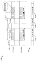
도 12 는, 버스 (430) 에 연결된 디바이스들 (402, 420, 422a-n) 이 I2C 디바이스를 포함할 때 공유된 버스 (430) 상에서 CCIe 모드에서의 데이터 송신의 일 예를 나타내는 타이밍도 (1200) 이다. 이 예에서, CCIe 디바이스들은, 신호 선들 (418, 416) 을 구동하기 위해, I2C 디바이스에 의해 사용된 오픈-드레인 드라이버들 보다는, 푸시-풀 드라이버들을 이용한다. 신호 선들 (418, 416) 상에서 송신되는 심볼들의 시퀀스 (1206, 1208) 에서 데이터가 인코딩된다. 대략 초 당 14 메가비트들 (Mbps) 의 유효한 데이터 레이트가 심볼 레이트가 20MHz 일 때 CCIe 송신을 위해 달성될 수도 있다. 본 명세서에서 기술된 바와 같이, 19 비트들의 데이터가 12 심볼들의 시퀀스들 (1206, 1208) 로 변환될 수도 있고, 이는, 심볼들의 시퀀스 (1206 또는 1208) 에서의 각 심볼 주기 (t sym ) (1212) 에 대해 SDA 신호 (418) 및 SCL 신호 (416) 의 상태를 제어한다. 나타낸 바와 같이, 각 심볼 주기 (1212) 는 지속기간이 50ns 일 수도 있다. 하나의 예에서, 19 비트들은 3 비트의 오버헤드를 가지고 16 비트의 데이터를 포함한다.12 shows a timing diagram 1200 (FIG. 12) showing an example of data transmission in CCIe mode on a shared
심볼들의 연속적인 시퀀스들 (1206 및 1208) 사이의 타이밍은 I2C 디바이스들의 동작을 지배하는 프로토콜들을 만족하기 위해 요구되는 시간 주기들에 의해 지배될 수도 있다. 하나의 예에서, 시작 조건 (1210) 은 각 송신 (1206, 1208) 에 선행하고 적어도 260ns 의 지속기간 (t HD ) 을 갖는다. 시작 조건 (1210) 은, SCL 신호 (416) 가 하이를 유지하는 동안 SDA 신호 (418) 가 로우를 유지하도록 "1" 의 심볼 값에 의해 정의될 수도 있다. 시작 조건 (1210) 은, "3" 의 심볼 값에 의해 정의되는 바와 같이 양 신호들 (418 및 416) 이 하이 상태에 있을 때 최소 셋업 주기 (t SU ) (1216) 를 따를 수도 있다. 최소 셋업 주기 (t SU ) (1216) 는, 송신 (1206 또는 1208) 이 종결된 후에 시작될 수도 있고, 그 최소 셋업 주기 (t SU ) (1216) 는 적어도 260ns 동안 유지될 수도 있다. 따라서, 제 1 송신 (1206) 의 시작과 제 2 송신 (1208) 의 시작 사이의 최소 경과 시간 (1214) 은 다음과 같이 계산될 수도 있다:The timing between successive sequences of symbols 1206 and 1208 may be governed by the time periods required to satisfy the protocols governing the operation of the I2C devices. In one example, start
![]()
![]()
셋업과 시작 시간 사이에 신호 하강 시간 (t f ) 을 위해 추가적인, 공칭 20ns 가 포함될 수도 있다. 신호 하강 시간은 다음과 같이 계산될 수도 있다:An additional, nominal 20 ns may be included for the signal fall time ( t f ) between the setup and start time. The signal fall time may be calculated as: < RTI ID = 0.0 >
![]()
![]()
따라서, 19 비트의 데이터는 최소 1140ns 에서 송신될 수도 있고, 16 비트들이 12 심볼들에서 송신되기 때문에, 대략 16.7Mbps 의 대응하는 로 비트 레이트 및 대략 14.04Mbps 의 유효 비트 레이트를 갖는다.Thus, 19 bits of data may be transmitted at a minimum of 1140 ns, and since 16 bits are transmitted in 12 symbols, they have a corresponding low bit rate of approximately 16.7 Mbps and an effective bit rate of approximately 14.04 Mbps.
송신들 (1206 및 1208) 사이의 최소 필요 시간은, 오직 CCIe 디바이스들만이 통신에 수반될 때보다 I2C 디바이스들이 버스 (430) 상에 수용될 때 상당히 더 크게 된다. 도 12 는, I2C 디바이스들에 대해 백워드 호환성을 제공하기 위해 I2C 셋업 및 시작 주기들을 부가하는 증가된 시간 (1224) 을 나타내는 타이밍도 (1220) 를 포함한다.The minimum required time between transmissions 1206 and 1208 is significantly greater when I2C devices are accommodated on
도 13 은 버스 (430) 상의 디바이스들 (402, 420, 422a-n) 이 활성 I2C 디바이스를 포함하지 않을 때 CCIe 버스 (430) 상에서의 데이터 송신을 나타내는 타이밍도 (1300) 이다. 시작 조건들의 지속기간은 감소될 수도 있다. 이 예에서, 푸시-풀 드라이버들이 신호 선들 (418, 416) 을 구동하기 위해 사용된다. 22.86Mbps 의 링크 레이트가 20MHz 심볼 레이트와 함께 달성될 수도 있다. 12 심볼들의 시퀀스들 (1306, 1308) 은 16 비트의 데이터 및 3 비트의 오버헤드를 인코딩한다. 12 심볼들의 시퀀스들 (1306, 1308) 에서의 각 심볼은 각 심볼 주기 (t sym ) (1310) 에 대해 SDA 신호 (418) 및 SCL 신호 (416) 의 상태를 정의한다. 각 심볼 주기 (1310) 는 20MHz 심볼 클럭에 대해 지속기간이 50ns 일 수도 있다. 2-심볼 시퀀스 {3,1} 는 심볼들 (1306 및 1308) 의 연속적인 시퀀스들 사이의 주기 (1314) 에서 송신된다. 제 1 송신 (1306) 의 시작과 제 2 송신 (1308) 의 시작 사이의 최소 경과 시간 (1312) 은 다음과 같이 계산될 수도 있다:Figure 13 is a timing diagram 1300 illustrating data transmission on the
![]()
![]()
푸시-풀 드라이버들을 갖는 CCIe 디바이스들이 사용될 때, 19 비트의 데이터는 700ns 에서 송신될 수도 있어, 16 데이터 비트들이 각 12 심볼 워드 (1306, 1308) 에서 송신되기 때문에, 대략 22.86Mbps 의 유효 비트 레이트로 대략 27.1Mbps 의 로 비트 레이트를 제공한다.When CCIe devices with push-pull drivers are used, 19 bits of data may be transmitted at 700 ns so that 16 data bits are transmitted at each of the 12 symbol words 1306 and 1308, resulting in an effective bit rate of approximately 22.86 Mbps Providing a bit rate of approximately 27.1 Mbps.
도 14 는 CCIe 인터페이스로서 구성되는 직렬 버스 (430) 와 연관된 특정 양태들을 나타낸다. 타이밍도 (1400) 는 도 5 에서 나타낸 CCIe 송신기 (500) 및 수신기 (520) 와 연관된 시그널링에 대응한다. 타이밍도 (1400) 는, 데이터 송신 동안 SDA 선 (418) 및 SCL 선 (416) 상에서 송신되는 심볼들의 시퀀스 (1408) 에 송신 클럭 (TXCLK) (1422) 가 임베딩되는 일 예를 나타낸다. 하나의 예에서, 클럭 정보는 천이 클럭 트랜스코딩을 이용하여 심볼들의 시퀀스 (1408) 에서 임베딩될 수도 있다. 예를 들어, 물리적 링크 (430) 를 통해 송신될 데이터 (510) 는 송신된 심볼들 (1408) 의 매 심볼 사이클 후에 상태 변화가 발생하도록 트랜스코딩된다. 그 결과로서, TXCLK (1422) 는, 예를 들어 심볼 S7 (1408d) 과 연관된 심볼 경계들 (1414 및 1416) 을 포함하는, 매 심볼 사이클의 심볼 경계들에서 발생하는 심볼 상태들의 변화들에서 임베딩될 수 있다. 수신기 (520) 는 송신된 심볼들 (1408) 의 시퀀스에서 각 심볼 경계 (1414, 1416) 에서 상태 천이로부터 복원된 클럭 정보로부터 수신 클럭 (RXCLK) (1412) 을 발생시킬 수 있다. 수신기 (520) 는 그 다음, 원래의 데이터 (530) 를 획득하기 위해 송신된 심볼들 (1408) 의 트랜스코딩을 거꾸로 할 수 있다. 이것은 I2C 버스 (430) 의 양 선들이 데이터를 전송하기 위해 이용되도록 허용한다. 추가적으로, 심볼 레이트는, 그것이 더 이상 클럭 및 데이터 신호들 사이에서 (도 11 에서 도시된 바와 같이) 셋업 및 유지 시간을 가질 필요가 없기 때문에, 상당히 증가될 수 있다.FIG. 14 illustrates specific aspects associated with
타이밍도 (1400) 에서 묘사된 예에서, 데이터 (510) 는 12-심볼 시퀀스들 또는 간격들 (1406) 에서 송신되는 심볼들의 스트림 (1408) 에서 인코딩될 수도 있다. 각 12-심볼 시퀀스 (1406) 는 시작 심볼 (1408a) 및 종결 또는 셋업 심볼 (1408c) 을 포함한다. 셋업 심볼 (1408c) 과 시작 심볼 (1408a) 의 결합은 CCIe 버스 상에서 송신되는 12 심볼들의 시퀀스들 (1406) 사이에 심볼들의 시퀀스 {3, 1} 를 형성한다. 본 명세서에서 기술된 바와 같이, 심볼의 시퀀스 (1406) 에서의 임의의 2 개의 연속적인 심볼들은, 수신기가 12-심볼 시퀀스 (1406) 에서의 심볼 경계들 (1414, 1416) 에서 발생하는 심볼 천이들로부터 RXCLK (1412) 를 도출할 수도 있도록, 공유된 버스 (430) 상에서 상이한 시그널링 상태들을 생성한다. 본 명세서에서 기술된 바와 같이, 심볼들 사이의 천이들은 천이 넘버들 (1410) 로부터 식별될 수도 있다. CCIe 인코더는 12 심볼들의 시퀀스 (1408), 시작 심볼 (1408a), 및 셋업 심볼 (1408b) 을 생성할 수도 있다.In the example depicted in timing diagram 1400,
특정 양태들에 따르면, 직렬 버스 (430) 는 동일 시간에서 I2C 디바이스들 및 CCIe 디바이스들 양자를 지원할 수 있다. 본 명세서에서 언급된 바와 같이, I2C 통신 모드들에 대해 SCL 신호 선 (416) 상에서 클럭 신호로서 송신될 클럭 정보는 심볼 천이들 내에 임베딩될 수 있고, 이에 의해, 심볼 정보를 반송하기 위해 이용되도록 하는 SCL 신호 선 (416) 의 이용을 허용한다. I2C 프로토콜의 특정 시그널링 특성들은 I2C 및 CCIe 모드들에 대해 공유된 버스 (430) 의 작동성을 가능하게 하도록 레버리지될 수도 있다. 예를 들어, I2C 프로토콜은, I2C 호환가능한 슬레이브 노드들이, SCL 라인 (416) 이 하이인 동안 SDA 라인 (418) 상에서 하이에서 로우로의 천이가 발생할 때 일어나는, 시작 조건의 수신 시에 그들의 버스 로직을 리셋하여야만 한다.According to certain aspects, the
CCIe 및 I2C 통신을 위해 동작가능한 버스 상에서의 시그널링의 예Example of Signaling on a Bus Operable for CCIe and I2C Communications
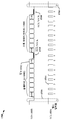
도 15 는 I2C 1-바이트 데이터 기록 동작을 예시하는 타이밍도 (1500) 이다. I2C 마스터 노드는, I2C 버스 (430) 상의 어느 슬레이브 노드가 마스터 노드가 액세스하기를 원하는 슬레이브 노드인지를 나타내기 위해 SDA 라인 (418) 상에서 7-비트 슬레이브 ID (1502) 를 송신하고, 이어서, 동작이 판독 동작인지 기록 동작인지 여부를 나타내는 판독/기록 비트 (1512) 를 송신한다. 판독/기록 비트 (1512) 는 기록 동작을 나타내기 위해 로직 0 에 있고, 판독 동작을 나타내기 위해 로직 1 에 있다. 오직 ID 가 7-비트 슬레이브 ID (1502) 에 매칭하는 슬레이브 노드만이 기록 (또는 판독) 동작에 응답할 수 있다. I2C 슬레이브 노드가 그 자신의 ID (1502) 를 검출하기 위해, 마스터 노드는 SCL 라인 (416) 상에서 8 클럭 펄스들과 함께 SDA 라인 (418) 상에서 적어도 8-비트들을 송신한다. 이러한 행동은 레거시 I2C 슬레이브 노드들이 CCIe 동작들에 반응하는 것을 방지하기 위해 CCIe 동작 모드들에서 데이터를 송신하기 위해 이용된다.15 is a timing diagram 1500 illustrating an I2C 1-byte data write operation. The I2C master node sends a 7-
도 16 은 레거시 I2C 슬레이브 노드 상에서의 시작 조건 (1606, 1608 또는 1610) 의 영향을 나타내는 하나의 예 (1600) 를 제공하고, 여기서, 시작 조건 (1606, 1608 또는 1612) 은, SCL 라인 (416) 이 하이 시그널링 상태에 있는 동안 SDA 라인 (418) 상에서 하이에서 로우로의 시그널링 상태 천이에 의해 표시된다. 이 예 (1600) 에서, 특정 시작 조건 (1608 또는 1612) 이, 완전한 7-비트 슬레이브 ID 가 송신되기 전까지 검출될 수도 있다. 결과적인 불완전한 슬레이브 ID (1602, 1604) 는 임의의 슬레이브 디바이스에 의해 인식되지 않는다. 동작에서, SCL 라인 (416) 상에서 오직 6 펄스들 (1612) 을 전송한 후에 시작 조건 (1608, 1610) 을 발행하는 마스터 노드의 효과는, 모든 레거시 I2C 슬레이브 노드들로 하여금, SDA 라인 (418) 상에서 그들 각각의 I2C 슬레이브 ID 를 인식하는 가능성이 발생하기 전에 그들의 버스 로직을 리셋하게 하는 것을 포함한다. 다르게 말하면, 2 개의 시작 조건들 (1606, 1608 및/또는 1610) 사이에 전송된 SDA 라인 (418) 상의 6-비트 시퀀스들 (1602, 1604) 이 슬레이브 노드들 중 어느 것에 의해서도 유효한 슬레이브 ID 로서 디코딩되지 않는다. 그 결과로서, 레거시 I2C 슬레이브 노드들은 불완전한 슬레이브 ID 들 (1602, 1604) 에 응답하도록 기대되지 않는다.Figure 16 provides an example 1600 illustrating the effect of a
도 16 은, CCIe 모드에서의 데이터 통신을 위한 I2C 버스의 SCL 라인 (416) 과 SDA 라인 (418) 의 결합의 이용을 나타내는 일 예 (1620) 를 또한 포함한다. CCIe 심볼은 I2C 송신을 위해 SCL 라인 (416) 상에서 송신되는 클럭 신호 (1614) 의 각 토글에 대응하는 시간에서 송신될 수도 있다. 2 개의 시작 조건들 (1608, 1610) 사이에서 송신되는 클럭 토글들의 넘버는 따라서 각 CCIe 송신을 위해 송신될 수도 있는 심볼들의 넘버를 정의할 수도 있다. 따라서, 12 심볼 송신들 (1622, 1624) 은, 임의의 슬레이브 노드들로 하여금 I2C 슬레이브 ID 로서 시퀀스를 검출하게 함이 없이, 불완전한 슬레이브 ID (1602, 1604) 와 동등한 6-SCL 펄스 시퀀스 동안 이용가능한 12 시그널링 상태들에서 제공될 수도 있다.16 also includes an example 1620 that illustrates the use of the combination of
SCL 라인 (416) 상의 천이와 일치하여 SDA 라인 (418) 상에서 발생하는 천이들은, 이러한 천이들을 시작 조건으로서 해석할 수도 있는, 레거시 I2C 디바이스들에 대해 중요하지 않다. 하지만, 레거시 I2C 디바이스는, I2C 슬레이브 노드의 버스 로직 검출을 리셋하는, 나중에 일어나는 유효한 시작 조건 (1628, 1630) 을 검출한다. I2C 슬레이브 노드들은 또한, CCIe 송신들 (1622, 1624) 동안 일어나는 몇몇 SDA 천이들을 정지 조건으로서 해석할 수도 있지만, CCIe 송신들 (1622, 1624) 내에서의 이러한 정지 조건의 검출은 단지 불완전한 SID (1602, 1604) 의 이른 종결을 야기할 뿐이다. 유사하게, CCIe 송신들 (1622, 1624) 동안 시작 조건의 검출은 슬레이브 노드들의 I2C 기능에 의해 리셋되는 버스 로직의 퍼포먼스 (performance) 를 야기한다.Transitions occurring on
따라서, 레거시 I2C 슬레이브 노드들은, 불완전한 I2C 슬레이브 ID (1602, 1604) 로서 6 SCL 펄스 시퀀스와 연관된 12 심볼 CCIe 송신들 (1622, 1624) 을 무시하도록 기대될 수 있다는 것은 명백하다. 따라서, 시작 조건들 (1606, 1608, 및 1610) 사이에서 이용가능한 12 SCL 토글들 동안, 열두개의 (12) 심볼들은 SCL 라인 (416) 및/또는 SDA 라인 (418) 상에서 송신될 수도 있다.Thus, it is clear that legacy I2C slave nodes can be expected to ignore 12-symbol CCIe transmissions 1622, 1624 associated with the 6 SCL pulse sequence as incomplete I2C slave IDs 1602, 1604. Thus, twelve (12) symbols may be transmitted on the
I2C 버스의 SCL 라인 (416) 및/또는 SDA 라인 (418) 은, 클럭 신호가 심볼 천이들 내에 임베딩되었을 때 CCIe 모드에서의 데이터 송신을 위해 활용될 수도 있다. 그 결과로서, SDA 라인 (418) 및 SCL 라인 (416) 은, 레거시 I2C 슬레이브 노드 기능성에 영향을 미침이 없이 그리고 CCIe-가능 노드들로부터 레거시 I2C 슬레이브 노드들을 분리하기 위해 브릿지 디바이스를 이용함이 없이, 2 개의 연속적인 시작 조건들 (1626, 1628 및/또는 1630) 사이에서 임의의 무작위의 12 개의 심볼들을 송신하기 위해 이용될 수 있다. I2C 모드에서, 시작 조건은 오직 I2C 마스터에 의해서만 전송되는 반면, CCIe 모드에서 12-심볼 워드를 송신하는 어느 노드에 의해서든지 시작 조건이 전송된다.The
도 17 은 동일한 2-선 직렬 버스 (430) 를 이용하여 통신할 수 있는 복수의 디바이스들 (1702, 1722 및 1742) 을 포함하는 시스템 (1700) 을 나타내는 블록도이다. 하나의 예에서, 2-선 직렬 버스 (430) 는 CCIe 프로토콜들에 따라 2 개 이상의 디바이스들 (1702, 1722) 사이에서의 통신을 지원하기 위해 하나의 모드에서 이용될 수도 있는 한편, 다른 모드에서, 2-선 직렬 버스 (430) 는 I2C 프로토콜들에 따라 하나 이상의 디바이스들 (1702, 1722, 및/또는 1742) 사이에서의 통신을 지원하기 위해 이용될 수도 있다. 따라서, 2-선 직렬 버스 (430) 상의 시그널링은, 2-선 직렬 버스 (430) 에 커플링된 디바이스들 (1702, 1722 및 1742) 이 송신 모드에 관계없이, 데이터 송신들 동안 신호 타이밍의 결과로서 서로 간섭하지 않는 것을 보장하기 위해 본 명세서에서 개시된 소정의 기술들을 채용할 수도 있다.17 is a block diagram illustrating a
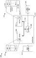
나타낸 간단한 예에서, I2C 슬레이브 디바이스 (1742) 는 I2C 프로토콜들에 따라 통신 가능할 수도 있고, 버스 마스터 디바이스 (1702) 는 I2C 및 CCIe 프로토콜들에 따라 통신 가능하고, CCIe 슬레이브 디바이스 (1722) 는 CCIe 프로토콜들에 따라, 그리고 어쩌면 CCIe 및 I2C 프로토콜들에 따라 통신 가능하다. 일부 경우들에서, CCIe 디바이스 (1702 및/또는 1722) 는 CCIe 동작 모드들 동안 직렬 버스 상에서 슬레이브 또는 마스터로서 동작할 수도 있다. 2-선 직렬 버스 (430) 는 도 3 에서 도시된 바와 같이 다른 디바이스들에 커플링될 수도 있음이 이해될 것이다. 장치 (1700) 는, 무선 모바일 디바이스, 모바일 텔레폰, 모바일 컴퓨팅 시스템, 무선 텔레폰, 노트북 컴퓨터, 태블릿 컴퓨팅 디바이스, 미디어 플레이어, 게이밍 디바이스, 어플라이언스, 웨어러블 컴퓨팅 디바이스 등에 내장될 수도 있다.In the simple example shown, I2C slave device 1742 may be communicable according to I2C protocols,
CCIe 디바이스들 (1702, 1722) 은 시스템 (1700) 에서 하나 이상의 특정 또는 지정된 기능들을 서빙할 수도 있다. 예를 들어, CCIe 디바이스들 (1702, 1722) 은, 디스플레이, 이미지 센서, 카메라, 키보드, 터치스크린 센서, 마우스 또는 다른 포인터, 시청각 코덱, 모뎀, 글로벌 포지셔닝 센서, 모션 검출기, 및 다른 디바이스들과 같은, 사용자 인터페이스의 엘리먼트들 또는 시스템 (1700) 을 채용하는 장치의 컴포넌트들을 제어 또는 포함하는 주변 모듈들 또는 회로들 (1704, 1724) 을 포함할 수도 있다. 또한, CCIe 디바이스들 (1702, 1722) 은, 스토리지 (1706, 1726), 프로세싱 회로 및/또는 제어 로직 (1710, 1730), 트랜시버 (1714, 1734), 및 라인 드라이버들/수신기들 (1716, 1718, 1736, 1738) 을 포함할 수도 있다. 프로세싱 회로 및/또는 제어 로직 (1710, 1730) 은 상태 머신, 시퀀서, 신호 프로세서 또는 범용 프로세서와 같은 프로세서를 포함할 수도 있다. 트랜시버 (1714, 1734) 는, 타이밍, 제어 로직, 일반 로직, CDR, 인코딩, 및 디코딩 회로들 및/또는 디바이스들을 포함하는, 소정의 회로들 및 모듈들과 함께, 수신기 (Rx) 및 송신기 (Tx) 를 포함할 수도 있다. 트랜시버 (1714, 1734) 는 상태 구성을 유지하기 위해 그리고 데이터 버퍼들을 제공하기 위해 이용되는 스토리지를 포함할 수도 있다.The
클럭 발생 회로 (1712, 1732) 는 트랜시버 (1714, 1734) 내에 또는 그 외부에 제공될 수도 있고, 및/또는, I2C 및 CCIe 통신 모드들에 대한 데이터 송신 레이트들을 결정하기 위해 이용될 수 있는 송신 클럭 (TXCLK) 신호를 제공할 수도 있다. I2C 동작 모드에서 SCL 커넥터 (416) 는 클럭 발생 회로 (1712, 1732) 에 의해 제공된 클럭을 반송할 수도 있는 한편, CCIe 동작 모드들에서 타이밍 정보는 SCL 커넥터 (416) 와 SDA 커넥터 (418) 를 이용하여 송신되는 심볼들의 시퀀스들 내에 임베딩될 수도 있다.
스토리지 (1706, 1726) 는 데이터, 구성 정보, 상태, 및/또는 소프트웨어 코드 및/또는 명령들을 저장하기 위해 이용될 수 있는 컴퓨터 판독가능 매체 또는 프로세서를 포함할 수도 있다. 데이터는, 송신기 회로를 공급하는 버퍼들 및/또는 수신기 회로로부터 인입되는 데이터를 핸들링하는 버퍼들에서 저장될 수도 있다. 소프트웨어 코드 또는 명령들은, 프로세싱 회로 및/또는 제어 로직 (1710, 1730) 이 디바이스 (1702, 1722) 의 다양한 구성 엘리먼트들을 관리 또는 동작시키고 2-선 직렬 버스 (430) 의 현재 동작 모드에 따라 통신 프로토콜들을 핸들링하도록, 프로세싱 회로 및/또는 제어 로직 (1710, 1730) 를 구성 및/또는 그것들에 의해 실행될 수도 있다.
마스터 디바이스 (1702) 는, 2-선 직렬 버스 (430) 의 동작 모드들을 제어하는 것, 및 2-선 직렬 버스 (430) 에 커플링된 디바이스들이 다른 디바이스들과 통신하는 것을 허용하기 위해 필요한 것으로서 동작 모드들 사이를 스위칭하는 것을 담당할 수도 있다. 따라서, 마스터 디바이스 (1702) 는 2-선 직렬 버스 (430) 에 대한 액세스를 필요로하거나 요청하는 슬레이브 디바이스 (1722, 1742) 를 식별할 수 있는 하나 이상의 프로토콜들 (1708) 을 구현할 수도 있다. 마스터 디바이스 (1702) 는, I2C 슬레이브 (1742) 가 어드레싱되어야 할 때 I2C-모드 통신 트랜잭션을 개시할 수도 있고, CCIe 슬레이브 (1722) 가 어드레싱되어야 할 때 CCIe-모드 통신 트랜잭션을 개시할 수도 있다. 일부 상황들에서, 2 개 이상의 디바이스들이 동일한 트랜잭션에서 어드레싱될 수도 있고, 마스터 디바이스 (1702) 는 이러한 트랜잭션을 위해 통신의 모드를 결정할 수도 있다.The
도 18 은 I2C 및 CCIe 동작 모드들 양자를 위해 구성된 버스 마스터 (1702) 에 의해 수행되는 모드 제어의 소정의 예들을 나타낸다. 이 예에서, 공유된 직렬 버스 (430) 상의 소정의 일반 타이밍 및 시그널링 동작 양태들이 예시되고, 명령들 또는 콜들의 구조 및 콘텐츠는 본 명세서에서 예시된 개념들에 영향을 미침이 없이 애플리케이션들 사이에서 변화할 수도 있음이 이해될 것이다. 마찬가지로, 본 명세서에서 기술된 특정 양태들에 따라 구성된 시스템들의 작동성은, CDR 교정 송신들 (1810), 엔트리 워드들 (entry words) (1812), 엑시트 워드들 (exit words) (1814) 및/또는 엑시트 시퀀스들 (1816) 등과 같은 송신들의 콘텐츠들 또는 포맷에 의해 제한되거나 의존할 필요는 없다.18 shows certain examples of mode control performed by the
제 1 타이밍도 (1800) 에서 예시된 바와 같이, 프로토콜은, 공유된 버스 (430) 가 CCIe 와 I2C 모드들 사이에서 스위칭하게끔 하는 절차들 및 시그널링을 정의할 수도 있다.As illustrated in first timing diagram 1800, the protocol may define procedures and signaling to cause the shared
하나의 예에서, 마스터 디바이스 (1702) 는 공유된 직렬 버스 (430) 를 이용하여 CCIe 모드 통신을 확립, 유지 또는 천이하도록 위해 CCIe 모드 엔트리 명령 (1812) 을 송신할 수도 있다. CCIe 모드 엔트리 명령은 I2C 모드에 있는 동안 CCIe-가능 디바이스 (1722) 에 어드레싱될 수도 있고, 어드레싱된 디바이스는 그것의 송신 및 수신 회로 (1734) 를 CCIe 통신을 지원하도록 재구성할 수도 있다. 수반되는 통신 트랜잭션의 타입에 기초하여, CCIe-가능 디바이스 (1722) 는, 공유된 직렬 버스 (430) 상에서 송신되는 심볼들의 시퀀스에서 임베딩된 클럭 정보를 가지면서, 공유된 직렬 버스 (430) 의 양 선들 상에서의 송신을 위해 데이터를 인코딩 또는 디코딩할 수도 있다. 공유된 직렬 버스 (430) 에 커플링된 I2C 슬레이브 디바이스 (1742) 는 통상적으로 CCIe 트랜잭션을 무시한다. I2C 슬레이브 디바이스는 불완전한 슬레이브 ID 를 감지할 수도 있지만, I2C 시작 조건이 CCIe 송신들 사이에서 공유된 직렬 버스 (430) 상에서 송신될 때 그것의 수신 회로를 리셋할 것이다. 일부 상황들에서, 다른 어드레싱되지 않은 CCIe 디바이스들 (3141-314n) (도 3 참조) 은 CCIe 통신을 모니터링할 수도 있다.In one example, the
마스터 디바이스 (1702) 는 공유된 직렬 버스 (430) 상에서의 I2C 모드 통신으로 복귀하기 위해 CCIe 모드 엑시트 명령 (1814) 을 송신할 수도 있다. 하나의 예에서, 공유된 버스 (430) 는, CCIe 모드에 대한 엔트리 (1812) 가 실행된 후에, CCIe 모드로부터의 엑시트 (1814) 가 실행될 때까지 그리고 그 엑시트가 실행되지 않는 한, CCIe 동작 모드를 유지한다.The
또 다른 타이밍도 (1802) 는 CCIe 모드로의 진입에 영향을 미치기 위해 이용될 수도 있는 엔트리 시퀀스를 나타내는 일 예를 포함한다. CCIe 모드 엔트리 (1812) 는, 공유된 버스 (430) 가 I2C 모드에서 동작하고 있는 동안 송신되는 일반 콜의 일부로서 달성될 수도 있다. CCIe 모드가 진입된 후에, 적절한 슬레이브 식별자 (SID) (1818) 가 송신되고, 이어서 하나 이상의 CCIe-가능 슬레이브들 (1722) 을 식별하는 어드레스가 뒤따르고, 이어서, 데이터 송신들이 뒤따른다. 어드레스는 멀티-워드 어드레스일 수도 있고, 각각의 어드레스 워드 및 각각의 데이터 워드는, 임의의 I2C 슬레이브 디바이스 (1742) 로 하여금 공유된 직렬 버스 (430) 상에서 비활성으로 유지하게 하도록 하는 I2C 시작 명령에 의해 분리될 수도 있다.Another timing diagram 1802 includes an example representing an entry sequence that may be used to affect entry into the CCIe mode. The
유사하게, CCIe 모드 엑시트 (1814) 는, 공유된 버스 (430) 가 CCIe 모드에서 동작하고 있는 동안 송신된 일반 콜의 일부로서 제공된 CCIe 모드 엑시트 시퀀스 (1804) 에 의해 달성될 수도 있다. CCIe 엑시트 명령 (1814) 은 모든 CCIe 디바이스들 (1722, 및/또는 3141-314n) 로 하여금 I2C 동작 모드로 복귀하게 할 수도 있다. 따라서, CCIe-가능 노드들 (1702, 1722, 및/또는 3141-314n) 은, I2C 모드로부터 CCIe 모드로 그리고 CCIe 모드로부터 I2C 모드로 각각 스위칭함으로써 엔트리/엑시트 시퀀스들 (1802, 1804) 을 포함하는 일반 콜들에 응답할 수도 있다.Similarly, the
도 18 은 또한, CCIe 기록 데이터 시퀀스 또는 프로토콜 (1806), 및 CCIe 판독 데이터 시퀀스 또는 프로토콜 (1808) 의 일 예를 제공한다. CCIe 기록 데이터 프로토콜 (1806) 은, SID 에 의해 식별된 슬레이브 노드/디바이스 (1722, 및/또는 3141-314n) 에 무작위 수의 어드레스 워드들 및 데이터 워드들을 전송하기 위해 수행될 수도 있다. CCIe 판독 데이터 시퀀스 또는 프로토콜 (1808) 은, SID 에 의해 식별된 슬레이브 노드/디바이스 (1722, 및/또는 3141-314n) 로부터 1 내지 5 의 데이터 워드들을 판독하기 위해 수행될 수도 있다. 어드레스 워드들의 넘버는 무작위로 정의될 수도 있다.Figure 18 also provides an example of a CCIe recording data sequence or
일부 경우들에서, CDR 교정 프로토콜 (1810) 은, 표시된 CCIe 노드 (그 자신의 마스터 노드를 포함) 로 하여금 그것의 CDR 로직을 교정하게 하기 위해 그리고 링크 레이트를 최대화하기 위해 CCIe 마스터 노드레 의해 이용될 수도 있다. 이 목적을 위해, CCIe 마스터 노드는 또한 그 자신의 SID 를 가질 수도 있다. CCIe 워드들은 19-비트 정보를 반송하는 12-심볼들에서 전송될 수도 있다. CDR 교정 프로토콜을 제외하고는, 19-비트들 중 3 개의 최상위 비트들이 제어 정보와 같은 다른 정보에 대해 이용될 수도 있는 한편 19-비트들 중 16 개의 최하위 비트들이 데이터를 반송한다.In some cases, the
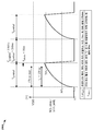
CCIe 인터페이스 (430) 의 데이터 레이트들은 푸시-풀 드라이버들의 선택 및/또는 이용에 의해 향상될 수도 있다. Fm+ 가능 I2C 버스 (430) 상에서의 CCIe 심볼 타이밍의 하나의 예를 나타내는 도 12 를 다시 참조한다. I2C Fm+ 모드를 위해 사용되는 동일한 물리적 드라이버에 의해 구동되는 CCIe 신호의 타이밍은 드라이버들의 상승 시간에 의해 제한될 수도 있고, 여기서, 상승 시간은 그것이 VDD 레벨의 30% 에서 70% 로 변화하기 위해 라인 전압을 취하는 시간이다. 도 19 는, CCIe 신호가 I2C Fm+ 모드를 위해 사용되는 동일한 물리적 드라이버에 의해 구동될 때 Fm+ 가능 I2C 버스 상에서의 CCIe 심볼 타이밍의 하나의 예를 나타내는 도이다. I2C Fm+ 를 위한 상승 시간은 120ns 이고, 0V 에서 70% 까지의 신호 전압 레벨을 위한 시간은 170ns 로서 계산될 수도 있다. 시그널링이 종종 마이크로컨트롤러 기반 동작들에 의해 핸들링되는 I2C 모드에서 이러한 상승 시간들은 만족스러울 수도 있지만, CCIe 모드에서는, 시그널링 동작들은 통상적으로 하드웨어에서 구현된다. 또한, 마이크로컨트롤러 기반의 또는 소프트웨어 동작되는 I2C 디바이스들은, 특히 SCL 선 (416) 이 로직 로우 상태에 있는 동안, 데이터를 프로세싱하기 위해 많은 사이클들을 필요로 할 수도 있다. 따라서, SCL 의 최소 로우 주기는 Fm+ 에 대해 1300ns 이상일 수도 있는 한편, I2C 프로토콜들에 의해 600ns 의 최소 하이 주기가 명시될 수도 있다.The data rates of the
본 명세서에서 개시된 특정 양태들에 따르면, CCIe 모드 디바이스들은 각 라인 (416, 418) 상의 로직 1 또는 로직 0 의 지속기간들의 차이들 또는 지속기간들의 평균에 집착하지 않을 수도 있다. CCIe 통신은 오직, 수신기가 하드웨어 기술들을 이용하여 로직 1 및 0 을 정확히 디코딩할 수 있는 것만을 요구하고, CCIe 는 더 이상 수개의 액션들을 수행하기 위해 긴 하이 또는 로우 주기들을 필요로 하지 않는다. 따라서, CCIe 시스템은 8ns 주기를 생성하는 125MHz 이상의 클럭을 이용할 수도 있다. 수신기가 비동기 입력 값들을 정확하게 검출하도록 하기 위해, 수신기는 적어도 3 번 동일한 값을 샘플링할 수도 있다. 하나의 예에서, CCIe 신호의 최소 하이 주기, tHIGH 는 30ns 로 설정될 수도 있고, 이는 125MHz 클럭과 연관된 최소 요구되는 24ns 를 훨씬 초과한다. 따라서, 170ns + 30ns (= 200ns) 하이 시간의 0-에서-70% 상승 시간은 최소 가능 심볼 시간이고, 결과적인 최대 심볼 레이트는 5MHz 이다.According to certain aspects disclosed herein, CCIe mode devices may not be stuck to the average of the differences or durations of the durations of
I2C 호환 버스를 통해 달성가능한 최대 CCIe 링크 레이트는 CCIe 가능 디바이스들에 의해 사용되는 드라이버들의 타입에 의해 영향을 받을 수도 있다. 하나의 예에서, 오픈-드레인 드라이버들 (2002,2004, 2006) (도 20 참조) 은 I2C 호환 버스 (430) 에 커플링된 CCIe 디바이스들에 의해 사용될 수도 있다. 이 예에서, 12 심볼들 (1206, 1208) 의 각 심볼은, 그 12 심볼들 (1206, 1208) 이 2400ns 에서 송신될 수도 있도록, 200 나노세컨드 (ns) 의 최소 심볼 시간 (1212) 에서 전송될 수도 있다. 추가적으로, 레거시 I2C 슬레이브 디바이스들이 공유된 버스 (430) 에 커플링될 때 I2C 타이밍 사양들에 부합하는 시작 조건들이 필요하다. 최소 시작 조건 셋업 시간 (1216) 및 최소 시작 조건 유지 시간 (1210) 은 I2C 고속-모드 플러스 (Fm+) 동작에 대해 260ns 의 특정된 최소 지속기간을 갖는다. 또한, SDA 라인 (418) 동작에 대해 허용되는 최대 하강 시간은 I2C Fm+ 에 대해 120ns 이고, 이는, SDA 라인 (418) 이 송신기 (500) 의 트랜지스터 (508) 에 의해 풀 다운될 때에도, 풀-업 저항기 (2002) 의 최대 상승 시간에 대응한다. CCIe 디바이스에 대해, SDA 라인 (418) 에 대한 하강 시간은 I2C 최대 하강 시간보다 상당히 더 빠른 하강 시간을 갖는 것으로 가정될 수도 있다. 예를 들어, CCIe 디바이스는 시작 조건에 대해 SDA 라인 (418) 에 대해 20ns 의 공칭 하강 시간을 제공할 수도 있다. 따라서, CCIe 디바이스는 2940ns 에서 시작 조건으로 CCIe 워드를 송신할 수도 있다. 19 비트들의 정보를 반송하는 CCIe 워드에 대한 로 비트 레이트는 다음과 같이 계산될 수도 있다:The maximum CCIe link rate achievable over an I < 2 > C compatible bus may be affected by the type of drivers used by CCIe capable devices. In one example, open-
19 bits / 2940 ns ![]()
![]()
하지만, 각 CCIe 워드는 16-비트들의 데이터 및 3 비트들의 오버헤드를 포함하여, 5.4Mbps (![]()
![]()
16 bits / 2940 ns ![]()
![]()
다른 예에서, CCIe 디바이스는 12-심볼 CCIe 워드를 송신하기 위해 오픈-드레인 드라이버들 대신에 푸시-풀 드라이버들을 이용할 수도 있다. 향상된 성능이 초래될 수도 있고, 적어도 16.7Mbps 의 링크 레이트가 20MHz 심볼 레이트에서 달성될 수 있다. CCIe 디바이스들은, CCIe 모드에서의 시작 조건들을 포함하는, I2C 동작들 동안 오픈-드레인 드라이버 거동을 모방할 수 있는 CMOS 푸시-풀 드라이버들을 사용할 수도 있다. CCIe 디바이스들은 푸시-풀 드라이버들의 PMOS 트랜지스터들을 선택적으로 디스에이블시킴으로써 오픈-드레인 드라이버 거동을 모방할 수도 있다. 대안적으로 또는 추가적으로, CCIe 디바이스들은 CCIe 모드에서 12-심볼들 동안 푸시-풀 드라이버들의 PMOS 트랜지스터들로부터 하이 신호 상태를 능동적으로 구동할 수도 있다. 그 결과로서, 50ns 심볼 주기 (1212) 가 이용되어, 600ns 에서 12-심볼 CCIe 워드들 (1206, 1208) 의 송신을 가능하게 할 수도 있다. t SU + t HD = 540 ns 주기의 시작 조건 지속기간 (셋업 시간 (1216) 및 유지 시간 (1210)) 이 유지된다. 이 구성에서, CCIe 모드 송신들에 대해 1140ns 에서 1 워드를 전송하는 것이 가능하고, 이는 다음과 같이 계산된 로 비트 레이트와 동등하다:In another example, a CCIe device may use push-pull drivers instead of open-drain drivers to transmit a 12-symbol CCIe word. Improved performance may result, and a link rate of at least 16.7 Mbps may be achieved at a 20 MHz symbol rate. CCIe devices may use CMOS push-pull drivers that can mimic the open-drain driver behavior during I2C operations, including startup conditions in CCIe mode. CCIe devices may mimic the open-drain driver behavior by selectively disabling the PMOS transistors of the push-pull drivers. Alternatively or additionally, the CCIe devices may actively drive a high signal state from the PMOS transistors of the push-pull drivers during 12-symbols in CCIe mode. As a result, a
19 bits / 1140 ns ![]()
![]()
하지만, 각 CCIe 워드는 16-비트들의 데이터 및 3 비트들의 오버헤드를 포함하여, 다음과 같이 계산되는 네트 데이터 레이트를 제공할 수도 있다:However, each CCIe word may provide a net data rate that includes 16-bit data and 3 bits of overhead, calculated as:
16 bits / 1140 ns ![]()
![]()
제 3 예에서, CCIe-가능 디바이스들은, 오직 CCIe-가능 디바이스들이 버스 (430) 에 커플링될 때 모든 송신들에 대해 CMOS 푸시-풀 드라이버들을 사용할 수도 있다. 그 결과로서, 심볼 주기 (1212) 는 대략적으로 50ns 로 단축될 수 있고, 600ns 에서의 12-심볼 CCIe 워드들 (1206, 1208) 의 송신은 600ns 에서 전송될 수 있다. I2C-호환 시작 조건이 요구되기 때문에, 시작 조건 주기는 50ns 심볼 주기 (1212) 와 동등한 지속기간에 대한 셋업 주기 (1216) 및 50ns 심볼 주기 (1212) 와 동등한 지속기간에 대한 유지 주기 (1210) 를 제공하여, 시작 조건을 100ns 의 지속기간으로 단축시킴으로써 구현될 수 있다. 이 예에서, 하나의 19-비트 워드는 700ns 에서 송신될 수 있고, 이는 27.1 Mbps (![]()
![]()
19 bits / 700 ns ![]()
![]()
하지만, 각 CCIe 워드는 16-비트들의 데이터 및 3 비트들의 오버헤드를 포함하여, 다음과 같이 계산되는 네트 데이터 레이트를 제공할 수도 있다:However, each CCIe word may provide a net data rate that includes 16-bit data and 3 bits of overhead, calculated as:
16 bits / 700 ns ![]()
![]()
다중 모드들의 통신을 지원하는 시스템의 제 1 예A first example of a system that supports communication in multiple modes
도 3, 도 4, 및 도 17 을 다시 참조하면, 시스템 또는 장치 (300, 1700) 는 다중모드 버스 (302) 에 의해 상호연결되는 복수의 디바이스들 (3041-304n, 312, 및 3141-314n) 을 채용할 수도 있다. 다중모드 버스 (302) 는 제 1 라인 (416) 및 제 2 라인 (418) 을 포함하는 2-선 직렬 버스를 포함할 수도 있다. 제 1 동작 모드는 직렬 버스 (430) 를 통한 데이터 송신들을 위해 제 1 프로토콜을 구현하고, 제 2 동작 모드는 직렬 버스 (430) 를 통한 데이터 송신들을 위해 제 2 프로토콜을 구현한다. 직렬 버스 (430) 는 I2C 및 CCIe 동작 모드들에서 동작할 수도 있다. 버스는 I2C-호환 버스일 수도 있다. 하나의 예에서, 직렬 버스 (430) 가 I2C 버스로서 동작할 때 제 1 라인 (416) 은 SCL 라인으로서 기능할 수도 있고, 직렬 버스 (430) 가 I2C 버스로서 동작할 때 제 2 라인 (418) 은 SDA 라인 (418) 으로서 기능할 수도 있다.Referring again to Figures 3, 4 and 17, a system or
제 1 동작 모드에서, 버스 (302) 에 커플링된 제 1 셋트의 디바이스들 (312 및/또는 3041-304n) 은 데이터 송신들을 위해 제 1 라인을 이용하고 제 1 클럭 신호를 위해 제 2 라인을 이용하도록 구성될 수도 있고, 제 2 동작 모드에서, 버스에 커플링된 제 2 셋트의 디바이스들 (312 및/또는 3141-314n) 은 데이터 송신들의 심볼 천이들 내에 제 2 클럭 신호를 임베딩하면서 데이터 송신들을 위해 제 1 라인 및 제 2 라인 양자를 이용하도록 구성될 수도 있다. 제 2 클럭 신호는 제 1 클럭 신호보다 더 큰 주파수를 가질 수도 있다.In a first mode of operation, a first set of
제 1 셋트의 디바이스들 (312 및/또는 3041-304n) 및 제 2 셋트의 디바이스들 (312 및/또는 3141-314n) 은 제 1 동작 모드 및 제 2 동작 모드 양자에서 적어도 제 1 라인을 동시에 모니터링할 수도 있다. 제 1 셋트의 디바이스들 (312 및/또는 3041-304n) 및 제 2 셋트의 디바이스들 (312 및/또는 3141-314n) 은 제 1 동작 모드 및 제 2 동작 모드 양자에서 적어도 제 2 라인을 동시에 모니터링할 수도 있다.The first set of
제 1 동작 모드에서, 제 1 셋트의 디바이스들 (312 및/또는 3041-304n) 로부터의 마스터 디바이스 (312) 는 버스의 제 1 라인을 통해 제 1 셋트의 디바이스들 (312 및/또는 3041-304n) 로부터의 슬레이브 디바이스들 (3041-304n) 에 데이터를 송신할 수도 있다.In a first mode of operation, the
제 2 동작 모드에서, 제 2 셋트의 디바이스들 (312 및/또는 3141-314n) 로부터의 마스터 디바이스 (312) 는 버스의 제 1 라인을 통해 제 2 셋트의 디바이스들 (312 및/또는 3141-314n) 로부터의 슬레이브 디바이스들 (3141-314n) 에 데이터를 송신할 수도 있다.In a second mode of operation, the
제 2 동작 모드에서, 제 1 셋트의 슬레이브 디바이스들 (3041-304n) 은 유효한 슬레이브 노드 어드레스의 검출을 억제하는 리셋 표시자를 제 1 라인 및 제 2 라인을 통해 수신할 수도 있다. 리셋 표시자는 예를 들어 I2C 시작 조건일 수도 있다. 제 2 동작 모드에서, 리셋 표시자가 제 1 라인 및 제 2 라인에서 삽입될 때 데이터 송신들은 주기적으로 인터럽트되고 (interrupted), 이에 의해, 제 1 셋트의 디바이스들 (3041-304n) 로 하여금 유효한 비트들의 시퀀스를 검출하기 이전에 그들의 버스 로직을 리셋하게 한다.In a second mode of operation, the slave devices 304 1 - 304 n of the first set may receive a reset indicator on the first line and the second line to inhibit detection of valid slave node addresses. The reset indicator may be, for example, an I2C start condition. In a second mode of operation, when the reset indicator is inserted in the first line and the second line, the data transmissions are periodically interrupted, thereby causing the first set of devices 304 1 - 304 n to be enabled To reset their bus logic before detecting a sequence of bits.
제 1 동작 모드에서, 마스터 노드 (312) 는 제 2 동작 모드로의 스위치 (switch) 를 표시하는 제 1 비트 시퀀스를 제 1 라인을 통해 제 2 셋트의 디바이스들 (3141-314n) 에 전송할 수도 있다. 마스터 노드 (312) 는 제 1 모드로의 스위치를 표시하는 엑시트 심볼 시퀀스를 버스 (430) 를 통해 제 2 셋트의 디바이스들 (3141-314n) 에 전송할 수도 있다.In a first mode of operation, the
제 2 동작 모드는 제 1 동작 모드보다 버스 (430) 를 통한 더 높은 송신 비트 레이트를 가질 수도 있다. 예를 들어, 제 1 동작 모드는 버스 (430) 를 통한 초 당 1 메가비트들의 최대 비트 레이트를 지원할 수도 있고, 제 2 동작 모드는 초 당 6.4 메가비트들의 최대 비트 레이트를 지원할 수도 있다. 다른 예에서, 제 1 동작 모드는 버스 (430) 를 통한 초 당 1 메가비트들의 최대 비트 레이트를 지원할 수도 있고, 제 2 동작 모드는 초 당 16.7 메가비트들의 최대 비트 레이트를 지원할 수도 있다.The second mode of operation may have a higher transmission bit rate over
제 2 셋트의 디바이스들 (3141-314n) 은 제 1 동작 모드 및 제 2 동작 모드 양자에서 동작 가능할 수도 있다.A second set of devices 314 1 - 314 n may be operable in both the first mode of operation and the second mode of operation.
하나의 예에서, 버스 (430) 는 제 2 셋트의 디바이스들 (3141-314n) 로부터의 제 1 디바이스를 포함하는 베이스밴드 프로세서에, 그리고, 제 2 셋트의 디바이스들 (3141-314n) 로부터의 제 2 디바이스를 포함하는 이미지 센서에 커플링된다. 버스 (430) 는 베이스밴드 프로세서와 이미지 센서 사이의 데이터 신호들을 제어할 수도 있다.In one embodiment,
일부 경우들에서, 제 2 셋트의 디바이스들 (3141-314n) 에서의 각 디바이스는, 데이터 비트들의 시퀀스를 복수의 M 개의 천이 넘버들로 변환하고, 각 천이 넘버를 순처적인 넘버들의 셋트로부터의 순차적인 넘버 (sequential number) 로 변환하며, 버스를 통해 그 순차적인 넘버를 송신하도록 적응된다. M 개의 천이 넘버들은 3진 디지트들로서 표현될 수도 있다. 순차적인 넘버는 어떤 2 개의 순차적인 넘버들도 동일하지 않는 것을 보장하기 위해 바로 이전의 순차 넘버로부터의 천이에 기초하여 천이 넘버로부터 선택될 수도 있다. 각 천이 넘버는 복수의 천이 넘버들을 순차적인 넘버로 변환함으로써 순차적인 넘버들의 셋트로부터의 순차적인 넘버로 변환될 수도 있다.In some cases, each device in the second set of devices 314 1 - 314 n converts the sequence of data bits to a plurality of M number of transition numbers, and for each transition number from a set of sequential numbers , And is adapted to transmit the sequential number through the bus. The M transition numbers may be represented as ternary digits. The sequential number may be selected from the transition number based on the transition from the immediately preceding sequential number to ensure that no two sequential numbers are equal. Each transition number may be converted to a sequential number from a set of sequential numbers by converting a plurality of transition numbers into sequential numbers.
다중 모드들의 통신을 지원하는 시스템의 제 2 예A second example of a system that supports multiple modes of communication
도 3, 도 4, 및 도 17 을 계속 참조하면, 시스템 또는 장치 (300, 1700) 는 다중모드 버스 (302) 에 의해 상호연결되는 복수의 디바이스들 (3041-304n, 312, 및 3141-314n) 을 채용할 수도 있다. 버스 (302) 는 제 1 라인 (418) 및 제 2 라인 (416) 을 갖는 2-선 직렬 버스 (430) 를 포함할 수도 있다. 버스는 I2C-호환 버스일 수도 있다. 제 1 동작 모드에서, 제 1 셋트의 디바이스들 (3041-304n, 312) 은 데이터 송신들을 위해 제 1 라인 (418) 을 이용하고 제 1 클럭 신호를 위해 제 2 라인 (416) 을 이용할 수도 있는 한편, 버스에 커플링된 제 2 셋트의 디바이스들 (312, 및 3141-314n) 은 제 2 동작 모드에서 데이터 송신들을 위해 제 1 라인 및 제 2 라인 양자를 이용하면서 데이터 송신들의 심볼 천이들 내에 제 2 클럭 신호를 임베딩하도록 구성될 수도 있다.3, 4, and 17, a system or
제 1 셋트의 디바이스들 (3041-304n, 312) 및 제 2 셋트의 디바이스들 (312 및 3141-314n) 은 제 1 동작 모드 및 제 2 동작 모드 양자에서 적어도 제 1 라인 (418) 을 동시에 모니터링할 수도 있다. 제 1 셋트의 디바이스들 (3041-304n, 312) 및 제 2 셋트의 디바이스들 (312, 및 3141-314n) 은 제 1 동작 모드 및 제 2 동작 모드 양자에서 적어도 제 2 라인 (416) 을 동시에 모니터링할 수도 있다.The first set of devices 304 1 -304 n 312 and the second set of
하나의 예에서, 제 1 셋트의 디바이스들 (3041-304n, 312) 로부터의 마스터 디바이스 (312) 는 제 1 동작 모드에서 버스 (430) 의 제 1 라인 (418) 을 통해 슬레이브 디바이스들 (3041-304n) 에 데이터를 송신한다. 다른 예에서, 제 2 셋트의 디바이스들 (312, 3141-314n) 로부터의 마스터 디바이스 (312) 는 제 2 동작 모드에서 버스 (430) 의 제 1 라인을 통해 슬레이브 디바이스들 (3141-314n) 에 데이터를 송신한다. 제 2 동작 모드는 제 1 동작 모드보다 버스 (430) 를 통한 더 높은 송신 비트 레이트를 가질 수도 있다. 하나의 예에서, 제 1 동작 모드는 버스 (430) 를 통한 초 당 1 메가비트들의 최대 비트 레이트를 가질 수도 있고, 제 2 동작 모드는 버스 (430) 를 통한 초 당 6.4 메가비트들의 최대 비트 레이트를 가질 수도 있다. 제 2 예에서, 제 1 동작 모드는 버스 (430) 를 통한 초 당 1 메가비트들의 최대 비트 레이트를 가질 수도 있고, 제 2 동작 모드는 버스 (430) 를 통한 초 당 16.7 메가비트들의 최대 비트 레이트를 가질 수도 있다. 제 2 클럭 신호는 제 1 클럭 신호보다 더 큰 주파수를 가질 수도 있다.In one example, the
제 1 동작 모드는 직렬 버스 (430) 를 통한 데이터 송신들을 위해 제 1 프로토콜을 구현하고, 제 2 동작 모드는 직렬 버스 (430) 를 통한 데이터 송신들을 위해 제 2 프로토콜을 구현한다.The first mode of operation implements a first protocol for data transmissions over the
제 1 셋트의 디바이스들은 제 2 동작 모드에서 유효한 슬레이브 노드 어드레스의 검출을 억제하는 리셋 표시자를 제 1 라인 (418) 및 제 2 라인 (416) 을 통해 수신할 수도 있다. 제 2 동작 모드에서, 리셋 표시자를 제 1 라인 (418) 및 제 2 라인 (416) 에 삽입함으로써 데이터 송신들은 주기적으로 인터럽트되어, 제 1 셋트의 디바이스들 (3041-304n) 로 하여금 유효한 비트들의 시퀀스를 검출하기 이전에 그들의 버스 로직을 리셋하게 한다.The first set of devices may receive a reset indicator on the
제 1 동작 모드 동안, 마스터 노드 (312) 는 제 2 동작 모드로의 스위칭이 이루어지는 것을 표시하는 제 1 비트 시퀀스를 제 1 라인을 통해 제 2 셋트의 디바이스들 (3141-314n) 에 전송할 수도 있다. 제 2 동작 모드 동안, 마스터 노드 (312) 는 제 1 동작 모드로의 스위칭이 이루어지는 것을 표시하는 엑시트 심볼 시퀀스를 버스 (430) 를 통해 제 2 셋트의 디바이스들 (3141-314n) 에 전송할 수도 있다. During the first mode of operation, the
하나의 예에서, 제 2 셋트의 디바이스들 (3141-314n) 은 제 1 동작 모드 및 제 2 동작 모드 양자에서 동작 가능할 수도 있다.In one example, the second set of devices 314 1 - 314 n may be operable in both the first mode of operation and the second mode of operation.
일부 경우들에서, 버스 (430) 는 제 2 셋트의 디바이스들 (3141-314n) 로부터의 제 1 디바이스를 포함하는 베이스밴드 프로세서에, 그리고, 제 2 셋트의 디바이스들 (3141-314n) 로부터의 제 2 디바이스를 포함하는 이미지 센서에 커플링된다. 버스 (430) 는 베이스밴드 프로세서 및 이미지 센서 사이의 데이터 신호들을 제어할 수도 있다. 제 2 셋트의 디바이스들 (3141-314n) 에서의 각 디바이스는, 데이터 비트들의 시퀀스를 복수의 M 개의 천이 넘버들로 변환하고, 각 천이 넘버를 순처적인 넘버들의 셋트로부터의 순차적인 넘버로 변환하며, 버스 (430) 를 통해 그 순차적인 넘버를 송신하도록 적응될 수도 있다. 순차적인 넘버는 어떤 2 개의 순차적인 넘버들도 동일하지 않는 것을 보장하기 위해 바로 이전의 순차 넘버로부터의 천이에 기초하여 천이 넘버로부터 선택될 수도 있다. 각 천이 넘버는 복수의 천이 넘버들을 순차적인 넘버로 변환함으로써 순차적인 넘버들의 셋트로부터의 순차적인 넘버로 변환될 수도 있다.In some cases, the
다중 모드들의 통신을 지원하는 시스템의 제 3 예A third example of a system that supports communication of multiple modes
도 3, 도 4, 및 도 17 을 계속 참조하면, 시스템 또는 장치 (300, 1700) 는 다중모드 버스 (302) 에 의해 상호연결되는 복수의 디바이스들 (3041-304n, 312, 및 3141-314n) 을 채용할 수도 있다. 버스 (302) 는 제 1 라인 (418) 및 제 2 라인 (416) 을 갖는 2-선 직렬 버스 (430) 를 포함할 수도 있다. 버스는 I2C-호환 버스일 수도 있다. 제 1 동작 모드에서, 제 1 셋트의 디바이스들 (3041-304n, 312) 은 데이터 송신들을 위해 제 1 라인 (418) 을 이용하고 제 1 클럭 신호를 위해 제 2 라인 (416) 을 이용할 수도 있는 한편, 버스에 커플링된 제 2 셋트의 디바이스들 (312, 및 3141-314n) 은 제 2 동작 모드에서 데이터 송신들을 위해 제 1 라인 및 제 2 라인 양자를 이용하면서 데이터 송신들의 심볼 천이들 내에 제 2 클럭 신호를 임베딩하도록 구성될 수도 있다.3, 4, and 17, a system or
동작에서, 프로세싱 회로는 송신기 및 수신기 회로로 및 로부터 데이터를 전송 및 수신하도록 구성될 수도 있고, 송신기 및 수신기 회로는 제 1 라인 (418) 및 제 2 라인 (416) 을 포함하는 버스 (430) 를 통해 통신하도록 구성될 수도 있다.In operation, the processing circuitry may be configured to transmit and receive data to and from the transmitter and receiver circuitry, and the transmitter and receiver circuitry may include a
송신기 및 수신기 회로는, 제 1 동작 모드에서, 데이터 송신들을 위해 제 1 라인 (418) 을 이용하고 제 1 클럭 신호를 위해 제 2 라인을 이용하도록 구성될 수도 있고, 제 2 동작 모드에서, 데이터 송신들의 심볼 천이들 내에 제 2 클럭 신호가 임베딩되도록 데이터를 송신하기 위해 제 1 라인 (418) 및 제 2 라인 (416) 양자를 이용하도록 구성될 수도 있다.The transmitter and receiver circuitry may be configured to use a
디바이스는, 버스에 커플링된 다른 디바이스들의 셋트와 공존할 수도 있지만, 제 1 동작 모드 및 제 2 동작 모드 양자 동안 적어도 제 1 라인 (418) 을 항상 모니터링하면서 오직 제 1 모드에서만 동작할 수도 있다. 디바이스는, 버스 (430) 에 커플링된 다른 디바이스들의 셋트와 공존할 수도 있지만, 제 1 동작 모드 및 제 2 동작 모드 양자 동안 적어도 제 2 라인 (416) 을 항상 모니터링하면서 오직 제 1 모드에서만 동작할 수도 있다.The device may coexist with a set of other devices coupled to the bus, but may only operate in the first mode, while always monitoring at least the
디바이스는 제 1 동작 모드에서 버스 (430) 의 제 1 라인 (418) 을 통해 슬레이브 디바이스에 데이터를 송신할 수도 있다. 디바이스는 제 2 동작 모드에서 버스 (430) 의 제 1 라인 (418) 및 제 2 라인 (416) 을 통해 슬레이브 디바이스에 데이터를 송신할 수도 있다. 제 1 동작 모드는 버스 (430) 를 통한 데이터 송신들을 위해 제 1 프로토콜을 구현할 수도 있고, 제 2 동작 모드는 버스 (430) 를 통한 데이터 송신들을 위해 제 2 프로토콜을 구현할 수도 있다.The device may transmit data to the slave device via the
송신기 및 수신기 회로는 제 1 동작 모드에서 동작하는 다른 디바이스들이 유효한 슬레이브 노드 어드레스를 검출하는 것을 억제하기 위해 제 2 동작 모드 동안 제 1 라인 (418) 및 제 2 라인 (416) 을 통해 리셋 표시자를 송신하도록 구성될 수도 있다. 리셋 표시자를 제 1 라인 (418) 및 제 2 라인 (416) 에 삽입함으로써 제 2 동작 모드 동안의 데이터 송신들은 주기적으로 인터럽트되어, 제 1 모드에서 동작하는 다른 디바이스들로 하여금 유효한 비트들의 시퀀스를 검출하기 이전에 그들의 버스 로직을 리셋하게 할 수도 있다.The transmitter and receiver circuits transmit a reset indicator via the
일부 예들에서, 송신기 및 수신기 회로는 제 1 모드 및 제 2 모드 양자에서 동작 가능한 다른 디바이스들에 대해 제 2 동작 모드로의 스위치를 나타내는 제 1 비트 시퀀스를 제 1 동작 모드에서 제 1 라인 (418) 을 통해 전송할 수도 있다. 마스터 노드 (312) 는 제 1 모드 및 제 2 모드 양자에서 동작 가능한 다른 디바이스들에 대해 제 1 동작 모드로의 스위치를 나타내는 엑시트 심볼 시퀀스를 제 2 동작 모드에서 버스 (430) 를 통해 전송할 수도 있다.In some instances, the transmitter and receiver circuit may be configured to transmit a first sequence of bits representing a switch to a second mode of operation to the
제 2 동작 모드는 제 1 동작 모드보다 버스를 통한 더 높은 송신 비트 레이트를 가질 수도 있다. 하나의 예에서, 제 1 동작 모드는 버스 (430) 를 통한 초 당 1 메가비트들의 최대 비트 레이트를 가지고, 제 2 동작 모드는 초 당 6.4 메가비트들의 최대 비트 레이트를 갖는다. 다른 예에서, 제 2 클럭 신호는 제 1 클럭 신호보다 더 큰 주파수를 가질 수도 있다.The second mode of operation may have a higher transmission bit rate over the bus than the first mode of operation. In one example, the first mode of operation has a maximum bit rate of 1 megabits per second through the
다중 모드들의 통신을 지원하는 시스템의 제 4 예A fourth example of a system that supports communication of multiple modes
도 3, 도 4, 및 도 17 을 계속 참조하면, 시스템 또는 장치 (300, 1700) 는 다중모드 버스 (302) 에 의해 상호연결되는 복수의 디바이스들 (3041-304n, 312, 및 3141-314n) 을 채용할 수도 있다. 버스 (302) 는 제 1 라인 (418) 및 제 2 라인 (416) 을 갖는 2-선 직렬 버스를 포함할 수도 있다. 버스는 I2C-호환 버스일 수도 있다. 제 1 동작 모드에서, 제 1 셋트의 디바이스들 (3041-304n, 312) 은 데이터 송신들을 위해 제 1 라인 (418) 을 이용하고 제 1 클럭 신호를 위해 제 2 라인 (416) 을 이용할 수도 있는 한편, 버스에 커플링된 제 2 셋트의 디바이스들 (312, 및 3141-314n) 은 제 2 동작 모드에서 데이터 송신들을 위해 제 1 라인 및 제 2 라인 양자를 이용하면서 데이터 송신들의 심볼 천이들 내에 제 2 클럭 신호를 임베딩하도록 구성될 수도 있다.3, 4, and 17, a system or
본 명세서에서 개시된 특정 양태들에 따르면, 마스터 디바이스 (312) 는, 버스에 커플링된 모든 디바이스들이, 제 1 클럭 신호를 위한 데이터 송신들 라인의 심볼 천이들 내에 제 2 클럭 신호를 임베딩하면서 데이터 송신들을 위해 제 1 라인 및 제 2 라인 양자를 이용하는 제 3 동작 모드에 따라 동작할 수 있는지 여부를 확인할 수도 있고, 버스에 커플링된 모든 디바이스들이 제 3 동작 모드에서 동작 가능한 경우에만, 디바이스들 (3041-304n, 312, 및 3141-314n) 이 제 3 동작 모드에서 동작되게끔 한다. 하나의 예에서, 제 3 동작 모드는 제 2 모드에 대해 감소된 시그널링 오버헤드를 제공할 수도 있다. 디바이스들의 셋트 (3041-304n, 312, 및 3141-314n) 는, 버스에 커플링된 모든 디바이스들 (3041-304n, 312, 및 3141-314n) 이 제 3 모드에서 동작할 수 있는 한, 또는, 버스에 커플링된 모든 활성 디바이스들 (3041-304n, 312, 및 3141-314n) 이 제 3 모드에서 동작할 수 있는 한, 제 3 모드에서 동작하도록 구성된다. 활성 디바이스는, 전원이 켜지고, 버스 (430) 에 커플링되고, 및/또, 버스 (430) 를 모니터링하고 있는 디바이스일 수도 있다. 디바이스들 (3041-304n, 312, 및 3141-314n) 은 제 1 동작 모드 및 제 2 동작 모드 양자에서 적어도 제 1 라인 (418) 을 동시에 모니터링할 수도 있다. 제 1 셋트의 디바이스들 (3041-304n, 312) 및 제 2 셋트의 디바이스들 (312, 및 3141-314n) 은 제 1 동작 모드 및 제 2 동작 모드 양자에서 적어도 제 2 라인 (416) 을 동시에 모니터링할 수도 있다.According to certain aspects disclosed herein, the
하나의 양태에서, 제 1 동작 모드는 버스 (430) 를 통한 데이터 송신들을 위해 제 1 프로토콜을 구현하고, 제 2 모드는 버스 (430) 를 통한 데이터 송신들을 위해 제 2 프로토콜을 구현하며, 제 3 모드는 버스 (430) 를 통한 데이터 송신들을 위해 제 3 프로토콜을 구현한다. 제 2 동작 모드는 레거시 디바이스들이, 유효한 슬레이브 노드 어드레스의 검출을 억제하는 리셋 표시자를 제 1 라인 (418) 및 제 2 라인 (416) 을 통해 수신하는 것을 허용할 수도 있다. 제 2 동작 모드에서, 버스 (430) 에 커플링된 레거시 디바이스들로 하여금 유효한 비트들의 시퀀스를 검출하기 이전에 그들의 버스 로직을 리셋하게 하는 리셋 표시자를 제 1 라인 (418) 및 제 2 라인 (416) 에 삽입함으로써 데이터 송신들은 주기적으로 인터럽트된다. 제 3 동작 모드에서, 제 1 라인 (418) 및 제 2 라인 (416) 에서 아무런 리셋 표시자도 전송되지 않는다.In one aspect, a first mode of operation implements a first protocol for data transmissions over
제 3 동작 모드는 제 2 동작 모드보다 버스 (430) 를 통한 더 높은 송신 비트 레이트를 가질 수도 있다. 제 3 동작 모드는 버스 (430) 를 통한 초 당 최대 27.1 메가비트들의 비트 레이트를 가질 수도 있다.The third mode of operation may have a higher transmission bit rate over
하나의 양태에서, 마스터 (312) 는, 버스에 커플링된 모든 디바이스들이 제 3 모드에 따라 동작할 수 있는지를 확인하고, 버스에 커플링된 모든 디바이스들 (3041-304n, 312, 및 3141-314n) 에 제 3 동작 모드에서 동작하도록 하는 명령을 전송할 수도 있다.In one aspect, the
CCIe 및 I2C 동작들을 위해 구성가능한 프로세싱 시스템들의 예Examples of configurable processing systems for CCIe and I2C operations
도 21 은 본 명세서에서 개시된 하나 이상의 기능들을 수행하도록 구성될 수도 있는 프로세싱 회로 (2102) 를 채용하는 장치에 대한 하드웨어 구현의 단순화된 예를 나타내는 개념도 (2100) 이다. 본 개시의 다양한 양태들에 따르면, 엘리먼트, 엘리먼트의 임의의 부분, 또는 엘리먼트들의 임의의 조합이 프로세싱 회로 (2102) 를 이용하여 구현될 수도 있다. 프로세싱 회로 (2102) 는 하드웨어 및 소프트웨어 모듈들의 몇몇 조합에 의해 제어되는 하나 이상의 프로세서들 (2104) 을 포함할 수도 있다. 프로세서들 (2104) 의 예들은, 마이크로프로세서들, 마이크로컨트롤러들, 디지털 신호 프로세서 (DSP) 들, 필드 프로그래머블 게이트 어레이 (FPGA) 들, 프로그래머블 로직 디바이스 (PLD) 들, 상태 머신들, 시퀀서들, 게이티드 로직, 이산 하드웨어 회로들, 및 이 개시물 전체를 통해 기술된 다양한 기능성을 수행하도록 구성된 다른 적합한 하드웨어를 포함한다. 하나 이상의 프로세서들 (2104) 은 특정 기능들을 수행하고 소프트웨어 모듈들 (2116) 중 하나에 의해 구성, 증강, 또는 제어될 수도 있는 특수화된 프로세서들을 포함할 수도 있다. 하나 이상의 프로세서들 (2104) 은 초기화 동안 로딩되는 소프트웨어 모듈들 (2116) 의 조합을 통해 구성될 수도 있고, 또한, 동작 동안 하나 이상의 소프트웨어 모듈들 (2116) 을 로딩 또는 언로딩함으로써 추가로 구성될 수도 있다.21 is a conceptual diagram 2100 illustrating a simplified example of a hardware implementation for an apparatus employing
도시된 예에서, 프로세싱 회로 (2102) 는 버스 (2110) 에 의해 일반적으로 표현된 버스 아키텍처와 함께 구현될 수도 있다. 버스 (2110) 는 프로세싱 회로 (2102) 의 특정 애플리케이션 및 전체 설계 제약들에 의존하여 임의의 수의 상호연결하는 버스들 및 브릿지들을 포함할 수도 있다. 버스 (2110) 는 하나 이상의 프로세서들 (2104), 스토리지 (2106) 를 포함하는 다양한 회로들을 함께 링크한다. 스토리지 (2106) 는 메모리 디바이스들 및 대용량 스토리지 디바이스들 (2104) 을 포함할 수도 있고, 본 명세서에서 컴퓨터 판독가능 매체들이라 지칭될 수도 있다. 버스 (2110) 는 또한, 타이밍 소스들, 타이머들, 주변장치들, 전압 조정기들, 및 전력 관리 회로들과 같은 다양한 다른 회로들을 링크할 수도 있고, 이들은 당해 기술 분야에서 잘 알려져 있고, 따라서, 그들의 일부는 더 이상 설명되지 않을 수도 있다. 버스 인터페이스 (2108) 는 버스 (2110) 와 라인 인터페이스 회로 (2112) 사이에 인터페이스를 제공할 수도 있다. 라인 인터페이스 회로 (2112) 는 직렬 버스와 같은 송신 매체를 통해 다양한 다른 장치와 통신하기 위한 수단을 제공한다. 장치의 성질에 의존하여, 사용자 인터페이스 (2118) (예컨대, 키패드, 디스플레이, 스피커, 마이크로폰, 조이스틱) 가 또한 제공될 수도 있고, 버스 (2110) 에 직접, 또는 버스 인터페이스 (2108) 를 통해서 통신가능하게 커플링될 수도 있다.In the illustrated example, the
프로세서 (2104) 는, 버스 (2110) 를 관리하는 것, 및 스토리지 (2106) 를 포함할 수도 있는 컴퓨터 판독가능 매체에 저장된 소프트웨어의 실행을 포함할 수도 있는 일반적인 프로세싱을 담당할 수도 있다. 이 점에서, 프로세서 (2104) 를 포함하는, 프로세싱 회로 (2102) 는 본 명세서에서 개시된 방법들, 기능들 및 기법들 중 어느 것을 구현하기 위해 이용될 수도 있다. 스토리지 (216) 는, 소프트웨어를 실행할 때 프로세서 (2104) 에 의해 조작되는 데이터를 저장하기 위해 이용될 수도 있고, 소프트웨어는 본 명세서에서 개시된 방법들 중 임의의 하나를 구현하도록 구성될 수도 있다.
프로세싱 회로 (2102) 내의 하나 이상의 프로세서들 (2104) 은 소프트웨어를 실행할 수도 있다. 소프트웨어는, 소프트웨어, 펌웨어, 미들웨어, 마이크로코드, 하드웨어 디스크립션 언어, 또는 기타로서 지칭되든지 간에, 명령들, 명령 셋트들, 코드, 코드 세그먼트들, 프로그램 코드, 프로그램들, 서브프로그램들, 소프트웨어 모듈들, 애플리케이션들, 소프트웨어 애플리케이션들, 소프트웨어 패키지들, 루틴들, 서브루틴들, 오브젝트들, 실행가능체들, 실행 스레드들, 절차들, 함수들, 알고리즘들 등을 의미하는 것으로 넓게 해석되어야 할 것이다. 소프트웨어는 스토리지 (2106) 에 또는 외부 컴퓨터 판독가능 매체에 컴퓨터 판독가능한 형태로 존재할 수도 있다. 컴퓨터 판독가능 매체 및/또는 스토리지 (2106) 는 비-일시적 (non-transitory) 컴퓨터 판독가능 매체일 수도 있다. 비-일시적 컴퓨터 판독가능 매체는, 예시로서, 자기 저장 디바이스 (예컨대, 하드 디스크, 플로피 디스크, 자기 스트립), 광학 디스크 (예컨대, 콤팩트 디스크 (CD) 또는 디지털 다기능 디스크 (DVD)), 스마트 카드, 플래시 메모리 디바이스 (예컨대, "플래시 드라이브", 카드, 스틱, 또는 키 드라이브), 랜덤 액세스 메모리 (RAM), 판독 전용 메모리 (ROM), 프로그래머블 ROM (PROM), 소거가능 PROM (EPROM), 전기적으로 소거가능한 PROM (EEPROM), 레지스터, 착탈형 디스크, 및 컴퓨터에 의해 액세스 및 판독될 수도 있는 소프트웨어 및/또는 명령들을 저장하기 위한 임의의 다른 적합한 매체를 포함한다. 컴퓨터 판독가능 매체 및/또는 스토리지 (2106) 는 또한, 예시로서, 반송파, 송신 라인, 및 컴퓨터에 의해 액세스 및 판독될 수도 있는 소프트웨어 및/또는 명령들을 송신하기 위한 임의의 다른 적합한 매체를 포함할 수도 있다. 컴퓨터 판독가능 매체 및/또는 스토리지 (2106) 는, 프로세싱 회로 (2102) 에, 프로세서 (2104) 에, 프로세싱 회로 (2102) 외부에 존재할 수도 있거나, 프로세싱 회로 (2102) 를 포함하는 다수의 엔티티들에 걸쳐 분산될 수도 있다. 컴퓨터 판독가능 매체 및/또는 스토리지 (2106) 는 컴퓨터 프로그램 제품에 포함될 수도 있다. 예시로서, 컴퓨터 프로그램 제품은 패키징 재료들에 컴퓨터 판독가능 매체를 포함할 수도 있다. 당해 기술분야에서 통상의 지식을 가진 자 (이하, '통상의 기술자' 라 함) 는, 특정 애플리케이션 및 전체 시스템에 부과된 전체적인 설계 제약들에 의존하여 이 개시물 전체를 통해 제시된 설명된 기능성을 어떻게 최선으로 구현할 수 있는지를 인식할 것이다.One or more of the
스토리지 (2106) 는, 본 명세서에서 소프트웨어 모듈들 (2116) 으로 지칭될 수도 있는, 로딩 가능한 코드 세그먼트들, 모듈들, 애플리케이션들, 프로그램들 등에서 유지 및/또는 조직화되는 소프트웨어를 유지할 수도 있다. 소프트웨어 모듈들 (2116) 의 각각은, 프로세싱 회로 (2102) 에 의해 설치 또는 로딩되거나 하나 이상의 프로세서들 (2104) 에 의해 실행될 때, 그 하나 이상의 프로세서들 (2104) 의 동작을 제어하는 런-타임 이미지 (2114) 에 기여하는 명령들 및 데이터를 포함할 수도 있다. 실행될 때, 어떤 명령들은 프로세싱 회로 (2102) 로 하여금 본 명세서에서 기술된 소정의 방법들, 알고리즘들 및 프로세스들에 따라 기능들을 수행하게 할 수도 있다.
소프트웨어 모듈들 (2116) 의 일부는 프로세싱 회로 (2102) 의 초기화 동안 로딩될 수도 있고, 이들 소프트웨어 모듈들 (2116) 은 본 명세서에 개시된 다양한 기능들의 수행을 가능하게 하도록 프로세싱 회로 (2102) 를 구성할 수도 있다. 예를 들어, 일부 소프트웨어 모듈들 (2116) 은 프로세서 (2104) 의 내부 디바이스들 및/또는 로직 회로들 (2122) 을 구성할 수도 있고, 라인 인터페이스 회로 (2112), 버스 인터페이스 (2108), 사용자 인터페이스 (2118), 타이머들, 연산 코프로세서들 등과 같은 외부 디바이스들에 대한 액세스를 관리할 수도 있다. 소프트웨어 모듈들 (2116) 은, 인터럽트 핸들러들 (interrupt handlers) 및 디바이스 드라이버들과 상호작용하고 프로세싱 회로 (2102) 에 의해 제공되는 다양한 리소스들에 대한 액세스를 제어하는 제어 프로그램 및/또는 오퍼레이팅 시스템을 포함할 수도 있다. 리소스들은 메모리, 스토리지 (2106), 프로세싱 시간, 라인 인터페이스 회로 (2112) 에 대한 액세스, 사용자 인터페이스 (2118) 등을 포함할 수도 있다.Some of the
프로세싱 회로 (2102) 의 하나 이상의 프로세서들 (2104) 은 다기능적일 수도 있고, 이에 의해, 소프트웨어 모듈들 (2116) 의 일부는 상이한 기능들, 또는 동일한 기능의 상이한 인스턴스들을 수행하도록 로딩 및 구성된다. 하나 이상의 프로세서들 (2104) 은, 예를 들어, 사용자 인터페이스 (2118), 라인 인터페이스 회로 (2112), 및 디바이스 드라이버들로부터의 입력들에 응답하여 개시되는 백그라운드 태스크들을 관리하도록 추가적으로 적응될 수도 있다. 다중 기능들의 수행을 지원하기 위해, 하나 이상의 프로세서들 (2104) 은 멀티태스킹 환경을 제공하도록 구성될 수도 있고, 이에 의해 복수의 기능들의 각각은 필요에 따라 또는 소망에 따라 하나 이상의 프로세서들 (2104) 에 의해 서비스되는 태스크들의 셋트로서 구현된다. 하나의 예에서, 멀티태스킹 환경은, 상이한 태스크들 사이에 프로세서 (2104) 의 제어를 패스하는 시간공유 프로그램 (2120) 을 이용하여 구현될 수도 있고, 이에 의해, 각 태스크는 임의의 미결 동작들의 완료 시에 및/또는 인터럽트와 같은 입력에 대해 응답하여 시간공유 프로그램 (2120) 에 그 하나 이상의 프로세서들 (2104) 의 제어를 리턴한다. 태스크가 하나 이상의 프로세서들 (2104) 의 제어를 가질 때, 프로세싱 회로는 제어 태스크와 연관된 함수에 의해 어드레싱된 목적들을 위해 유효하게 특수화된다. 시간공유 프로그램 (2120) 은 오퍼레이팅 시스템, 순환식으로 제어를 전송하는 메인 루프, 함수들의 우선순위화에 따라서 하나 이상의 프로세서들 (2104) 의 제어를 할당하는 함수, 및/또는 핸들링 함수에 하나 이상의 프로세서들 (2104) 의 제어를 제공함으로써 외부 이벤트들에 응답하는 인터럽트 구동된 메인 루프를 포함할 수도 있다.One or more of the
도 22 는 CCIe 버스 상에서의 데이터 통신들을 위한 방법을 나타내는 흐름도 (2200) 이다. 이 방법의 다양한 단계들은 예를 들어 도 1-8, 20, 22, 및/또는 24 에서 예시된 디바이스들 및 회로들의 몇몇 조합을 포함하는 송신기 디바이스에 의해 수행될 수도 있다.22 is a
블록 2202 에서, 디바이스는 비트들의 셋트로부터 천이 넘버를 생성할 수도 있다. 천이 넘버는 12 디지트 3진수를 포함할 수도 있다. 하나의 예에서, 디바이스는 비트들의 셋트로부터 천이 넘버를 생성할 수도 있다. 천이 넘버는 12 디지트 3진수일 수도 있다.At
블록 2204 에서, 디바이스는 그 천이 넘버를 심볼들의 시퀀스로 변환할 수도 있다. 심볼들의 시퀀스에서의 심볼들 사이의 천이드레서 타이밍 정보가 인코딩될 수도 있다. 심볼들의 시퀀스에서 인코딩된 타이밍 정보는 수신기가 심볼들의 시퀀스로부터 수신 클럭을 생성하는 것을 가능하게 한다. 천이 넘버는 3진수를 트랜스코더에 제공함으로써 심볼들의 시퀀스로 변환될 수도 있다.At
하나의 예에서, 트랜스코더는 3진수의 최상위 디지트를 먼저 수신하고, 3진수의 최하위 디지트는 마지막으로 트랜스코더에 의해 수신될 수도 있으며, 최상위 디지트와 최하위 디지트 사이의 중간 디지트들은 감소하는 순위의 순서로 트랜스코더에 제공된다. 다른 예에서, 트랜스코더는 3진수의 최하위 디지트를 먼저 수신하고, 3진수의 최상위 디지트는 마지막으로 트랜스코더에 의해 수신될 수도 있으며, 최상위 디지트와 최하위 디지트 사이의 중간 디지트들은 증가하는 순위의 순서로 트랜스코더에 제공된다.In one example, the transcoder first receives the highest digit of the ternary number, the lowest digit of the ternary number is finally received by the transcoder, and the intermediate digits between the highest digit and the lowest digit are in decreasing order To the transcoder. In another example, the transcoder may receive the least significant digit of the ternary number first, the most significant digit of the ternary number may finally be received by the transcoder, and the intermediate digits between the highest digit and the lowest digit may be in ascending order And is provided to the transcoder.
블록 2206 에서, 디바이스는, 2-선 직렬 버스가 제 1 동작 모드에서 동작될 때, 2-선 직렬 버스 상에서 심볼들의 시퀀스를 송신할 수도 있다. 심볼들의 시퀀스는, 2-선 직렬 버스가 제 2 동작 모드에서 동작될 때, 2-선 직렬 버스 상에서 통신하도록 구성된 디바이스에 의해 무시될 수도 있다. 2-선 직렬 버스에 대해 4 개의 시그널링 상태들이 정의될 수도 있다. 3진수의 각 디지트는 3 개의 이용가능한 심볼들 중 하나로부터 2-선 직렬 버스 상에서 송신될 다음 심볼을 선택 및/또는 표시할 수도 있다. 3 개의 이용가능한 심볼들의 각각은 2-선 직렬 버스 상에서 송신되고 있는 현재의 심볼과 상이할 수도 있다. 따라서, 연속적인 심볼들 사이의 각각의 천이는 2-선 직렬 버스의 시그널링 상태에서의 변화를 야기한다.At
하나의 예에서, 2-선 직렬 버스는 제 1 동작 모드에서 동작될 때 CCIe 통신을 지원하는 다목적 버스일 수도 있다. 제 2 동작 모드에 대해, 2-선 직렬 버스는 통신의 I2C 및또는 CCI 모드들을 지원할 수도 있다. 디바이스는, 제어 시퀀스가 2-선 직렬 버스 상에서 송신될 때 제 1 동작 모드로부터 제 2 동작 모드로의 변화를 야기하도록 구성 또는 적응될 수도 있다. CCIe 모드의 동작에서, I2C 시작 조건은 CCIe 동작 모드에서 2-선 직렬 버스 상에서 송신되는 심볼들의 시퀀스 사이에서 제공될 수도 있다. 시작 조건의 타이밍의 소정 양태들은, 오직 I2C 프로토콜들을 이용하여 통신할 수 있는 디바이스들을 포함하는, I2C 동작 모드를 위해 구성되는 다른 디바이스에서 수신 로직의 리셋을 야기할 수도 있다.In one example, the 2-wire serial bus may be a multipurpose bus that supports CCIe communication when operating in the first mode of operation. For the second mode of operation, the 2-wire serial bus may support I2C and / or CCI modes of communication. The device may be configured or adapted to cause a change from a first mode of operation to a second mode of operation when the control sequence is transmitted on a two-wire serial bus. In operation in the CCIe mode, the I2C start condition may be provided between the sequence of symbols transmitted on the 2-wire serial bus in the CCIe mode of operation. Certain aspects of the timing of the start condition may cause a reset of the receive logic at another device configured for the I < 2 > C operation mode, including devices capable of communicating using only I2C protocols.
하나의 예에서, 제 1 I2C 시작 조건은 2-선 직렬 버스 상에서 심볼들의 시퀀스가 송신되기 전에 2-선 직렬 버스 상에서 송신된다. 2-선 직렬 버스 상에서 심볼들의 시퀀스가 송신된 후에, 제 2 I2C 시작 조건이 2-선 직렬 버스 상에서 송신될 수도 있다. 제 1 및 제 2 I2C 시작 조건들 사이에 경과된 시간은 I2C 동작 모드들에서 어드레스 워드를 수신하기 위해 I2C 프로토콜들에 의해 요구되는 시간 미만일 수도 있다. 따라서, 2-선 직렬 버스를 모니터링하는 I2C 수신기는, 제 1 시작 조건 후에 그리고 제 2 I2C 시작 조건 전에 2-선 직렬 버스의 SCL 신호 선 상에서 최대 6 클럭 사이클들을 통상적으로 감지한다.In one example, a first I2C start condition is transmitted on a two-wire serial bus before a sequence of symbols is transmitted on a two-wire serial bus. After the sequence of symbols is transmitted on the 2-wire serial bus, the second 12C start condition may be transmitted on the 2-wire serial bus. The elapsed time between the first and second I2C start conditions may be less than the time required by the I2C protocols to receive the address word in I2C operating modes. Thus, an I < 2 > C receiver monitoring a two-wire serial bus typically senses up to six clock cycles on the SCL signal line of the two-wire serial bus after the first start condition and before the second I2C start condition.
도 23 은 프로세싱 회로 (2302) 를 채용하는 장치에 대한 하드웨어 구현의 단순화된 예를 나타내는 도 (2300) 이다. 프로세싱 회로는 통상적으로, 마이크로프로세서, 마이크로컨트롤러, 디지털 신호 프로세서, 시퀀서, 상태 머신 등 중 하나 이상을 포함할 수도 있는 프로세서 (2316) 를 갖는다. 프로세싱 회로 (2302) 는 일반적으로 버스 (2320) 에 의해 표현되는 버스 아키텍처로 구현될 수도 있다. 버스 (2320) 는 프로세싱 회로 (2302) 의 특정 애플리케이션 및 전체 설계 제약들에 의존하여 임의의 수의 상호연결 버스들 및 브릿지들을 포함할 수도 있다. 버스 (2320) 는, 프로세서 (2316), 모듈들 또는 회로들 (2304, 2306, 2308 및 2310), 복수의 커넥터들 또는 선들을 포함하는 다중-레인 CCIe 버스 (2314) 를 통해 통신하도록 구성가능한 라인 인터페이스 회로 (2312), 및 컴퓨터 판독가능 저장 매체 (2318) 에 의해 표현되는 하나 이상의 프로세서들 및/또는 하드웨어 모듈들을 포함하는 다양한 회로들을 함께 링크한다. 버스 (2320) 는 또한, 타이밍 소스들, 주변장치들, 전압 조정기들, 및 전력 관리 회로들과 같은 다양한 다른 회로들을 링크할 수도 있고, 이들은 당해 기술분야에서 잘 알려져 있고, 따라서, 더 이상 설명되지 않을 것이다.FIG. 23 is a drawing 2300 illustrating a simplified example of a hardware implementation for an apparatus employing
프로세서 (2316) 는 컴퓨터 판독가능 저장 매체 (2318) 상에 저장된 소프트웨어의 실행을 포함하는, 일반적인 프로세싱을 담당한다. 소프트웨어는, 프로세서 (2316) 에 의해 실행될 때, 프로세싱 회로 (2302) 로 하여금 특정 장치에 대해 상기 설명된 다양한 기능들을 수행하게 한다. 컴퓨터 판독가능 저장 매체 (2318) 는 또한, 다중-레인 CCIe 버스 (2314) 를 통해 송신되는 심볼들로부터 디코딩되는 데이터를 포함하는, 소프트웨어를 실행할 때 프로세서 (2316) 에 의해 조작되는 데이터를 저장하기 위해 이용될 수도 있다. 프로세싱 회로 (2302) 는 모듈들 및/또는 회로들 (2304, 2306 및 2308) 중 적어도 하나를 더 포함한다. 모듈들 및/또는 회로들 (2304, 2306, 2308 및 2310) 은, 프로세서 (2316) 에서 로딩, 구성 및 실행되고 컴퓨터 판독가능 저장 매체 (2318) 에 상주/저장되는 소프트웨어 모듈들, 프로세서 (2316) 에 커플링된 하나 이상의 하드웨어 모듈들, 또는 이들의 몇몇 조합일 수도 있다. 모듈들 및/또는 회로들 (2304, 2306 및 2308) 은 마이크로컨트롤러 명령들, 상태 머신 구성 파라미터들, 또는 이들의 몇몇 조합을 포함할 수도 있다.
하나의 구성에서, 무선 통신을 위한 장치 (2300) 는, 비트들의 세트로부터 천이 넘버를 생성하도록 구성되는 모듈 및/또는 회로 (2304), 그 천이 넘버를 심볼들의 시퀀스로 변환하도록 구성된 모듈 및/또는 회로 (2306), 및 2-선 직렬 버스의 시그널링 상태에서 심볼들의 시퀀스를 송신하도록 구성되는 모듈 및/또는 회로 (2308) 를 포함한다. 장치 (2300) 는 예를 들어 직렬 버스 (2314) 및/또는 장치 (2314) 의 동작 모드를 제어하는 모듈 및/또는 회로 (2310) 를 포함하는, 추가적인 모듈 및/또는 회로들을 포함할 수도 있다. 예를 들어, 모드 제어 모듈 및/또는 회로 (2310) 는 직렬 버스 (2314) 상에서 제어 시퀀스들을 송신하는 명령 생성 모듈을 포함하거나 그것과 협동할 수도 있다. 다른 예에서, 모드 제어 모듈 및/또는 회로 (2310) 는, 오픈-드레인 라인 드라이버들 또는 그것의 균등물들이 I2C 동작 모드에 그리고 푸시-풀 드라이버들이 CCIe 동작 모드에 있는 것을 가능하게 하기 위해 라인 인터페이스 회로 (2314) 의 재구성을 야기할 수도 있다.In one configuration, an
도 24 는 CCIe 버스 상에서의 데이터 통신들을 위한 방법을 나타내는 흐름도 (2400) 이다. 방법의 다양한 단계들은, 예를 들어 도 1-8, 20, 23 및/또는 24 에서 예시된 디바이스들 및 회로들의 몇몇 조합을 포함하는 CCIe 디바이스에서의 수신기 회로 및 모듈들을 이용하여 수행될 수도 있다.24 is a
단계 2402 에서, 디바이스는, 2-선 직렬 버스가 제 1 동작 모드에서 동작될 때 2-선 직렬 버스의 시그널링 상태에서의 천이들로부터 수신 클럭을 도출할 수도 있다. 2-선 직렬 버스는, 그 2-선 직렬 버스가 제 1 동작 모드에서 동작될 때, CCIe 통신을 동시에 지원하는 다목적 버스일 수도 있다. 2-선 직렬 버스는 제 2 동작 모드에서 I2C 통신을 지원할 수도 있다. 2-선 직렬 버스는 I2C, CCI 및/또는 CCIe 프로토콜들 중 하나 이상과 호환가능한 디바이스들과의 통신을 지원할 수도 있다.In
단계 2404 에서, 디바이스는 제 1 동작 모드에 따라 2-선 직렬 버스 상에서 송신되는 심볼들의 시퀀스를 수신하기 위해 수신 클럭을 이용할 수도 있다. 2-선 직렬 버스의 시그널링 상태에서의 천이들은 심볼들의 시퀀스에서의 심볼들 사이의 천이들에 대응할 수도 있다. 심볼들의 시퀀스는, 2-선 직렬 버스 상의 I2C 시작 조건을 결정하고, 수신 클럭에 의해 정의된 타이밍에 따라 2-선 직렬 버스로부터 12 심볼들을 수신함으로써 2-선 직렬 버스로부터 수신될 수도 있다.At
하나의 양태에서, 심볼들의 시퀀스는 2-선 직렬 버스가 제 2 동작 모드에서 동작될 때 2-선 직렬 버스 상에서 통신하도록 구성된 디바이스에 의해 무시될 수도 있다.In one aspect, the sequence of symbols may be ignored by the device configured to communicate on the 2-wire serial bus when the 2-wire serial bus is operated in the second mode of operation.
단계 2406 에서, 디바이스는 심볼들의 시퀀스로부터 천이 넘버를 생성할 수도 있다. 천이 넘버는 다중 디지트들을 가질 수도 있고, 그 다중 디지트들의 각각의 디지트는 심볼들의 시퀀스에서의 연속적인 심볼들의 쌍 사이의 천이를 나타낸다.In
단계 2408 에서, 디바이스는 그 천이 넘버로부터 데이터를 디코딩할 수도 있다. 천이 넘버는 12-디지트 3진수일 수도 있다. 2-선 직렬 버스에 대해 네개 (4) 의 시그널링 상태들이 정의될 수도 있다. 3진수의 각 디지트는 2-선 직렬 버스 상의 연속적인 시그널링 상태들의 쌍 사이의 관계를 나타낼 수도 있다. 심볼들의 시퀀스에서의 각 심볼은 2-선 직렬 버스의 시그널링 상태에 의해 정의되는 4 개의 심볼들 중 하나일 수도 있다. 3진수의 각 디지트는 심볼들의 시퀀스에서의 연속적인 심볼들의 쌍 사이의 관계를 정의할 수도 있다.In
도 25 는 프로세싱 회로 (2502) 를 채용하는 장치에 대한 하드웨어 구현의 단순화된 예를 예시하는 도 (2500) 이다. 프로세싱 회로는 통상적으로 마이크로프로세서, 마이크로컨트롤러, 디지털 신호 프로세서, 시퀀서, 상태 머신, 또는 기타 중 하나 이상을 포함하는 프로세서 (2516) 를 갖는다. 프로세싱 회로 (2502) 는 버스 (2520) 에 의해 일반적으로 표현되는 버스 아키텍처로 구현될 수도 있다. 버스 (2520) 는 프로세싱 회로 (2502) 의 특정 애플리케이션 및 전체 설계 제약들에 의존하여 임의의 수의 상호연결 버스들 및 브리지들을 포함할 수도 있다. 버스 (2520) 는 프로세서 (2516), 모듈들 및/또는 회로들 (2504, 2506 및 2508), 복수의 커넥터들 또는 선들을 포함하는 다중-레인 CCIe 버스 (2514) 를 통해 통신하도록 구성가능한 라인 인터페이스 회로 (2512), 및 컴퓨터 판독가능 저장 매체 (2518) 에 의해 표현된 하나 이상의 프로세서들 및/또는 하드웨어 모듈들을 포함한 다양한 회로들을 함께 링크시킨다. 버스 (2520) 는 또한 다른 회로들, 예컨대, 타이밍 소스들, 주변장치들, 전압 조정기들, 및 전력 관리 회로들을 링크할 수도 있으며, 이들은 당해 기술분야에서 잘 알려져 있으며, 따라서, 더 이상 설명되지 않을 것이다.25 is a
프로세서 (2516) 는 컴퓨터 판독가능 저장 매체 (2518) 상에 저장된 소프트웨어의 실행을 포함하는, 일반적인 프로세싱을 담당한다. 프로세서 (2516) 에 의해 실행될 때, 소프트웨어는 프로세싱 회로 (2502) 로 하여금 임의의 특정 장치에 대하여 위에 설명된 여러 기능들을 수행하게 한다. 컴퓨터 판독가능 저장 매체 (2518) 는 또한, 소프트웨어를 실행시킬 때 프로세서 (2516) 에 의해 조작되는, 다중-레인 CCIe 버스 (2514) 를 통하여 송신되는 심볼들로부터 디코딩되는 데이터를 포함한, 데이터를 저장하는데 이용될 수도 있다. 프로세싱 회로 (2502) 는 모듈들 및/또는 회로들 (2504, 2506 및 2508) 중 적어도 하나를 더 포함한다. 모듈들 및/또는 회로들 (2504, 2506 및 2508) 은 컴퓨터 판독가능 저장 매체 (2518) 상에 상주/저장되는, 프로세서 (2516) 에서 실행되는 소프트웨어 모듈, 프로세서 (2516) 에 커플링되는 하나 이상의 하드웨어 모듈들, 또는 이들의 몇몇 조합일 수도 있다. 모듈들 및/또는 회로들 (2504, 2506 및 2508) 은 마이크로컨트롤러 명령들, 상태 머신 구성 파라미터들, 또는 이들의 몇몇 조합을 포함할 수도 있다.
하나의 구성에서, 무선 통신을 위한 장치 (2500) 는, 2-선 직렬 버스의 시그널링 상태에서의 천이들로부터 수신 클럭을 도출하고 그 수신 클럭을 이용하여 2-선 직렬 버스로부터 심볼들의 시퀀스를 수신하도록 구성되는 CDR 회로 (2504), 심볼들의 시퀀스로부터 천이 넘버를 생성하도록 구성되는 모듈 및/또는 회로 (2506), 및 천이 넘버로부터 데이터를 디코딩하도록 구성되는 모듈 및/또는 회로 (2508) 를 포함한다. 2-선 직렬 버스의 시그널링 상태에서의 천이들은 심볼들의 시퀀스에서의 심볼들 사이의 천이들에 대응할 수도 있다. 천이 넘버는 다중 디지트들을 가질 수도 있고, 그 다중 디지트들의 각 디지트는 심볼들의 시퀀스에서의 연속적인 심볼들의 쌍 사이의 천이를 나타낸다.In one arrangement, a
도 26 은 버스를 채용하는 시스템 또는 디바이스에 관련된 방법을 나타내는 흐름도 (2600) 이다. 하나의 예에서, 디바이스는 제 1 라인 및 제 2 라인을 포함하는 버스, 버스에 커플링된 제 1 셋트의 디바이스들 및 버스에 커플링된 제 2 셋트의 디바이스들을 가질 수도 있다. 방법은 본 명세서에서 개시된 바와 같은 CCIe 버스 (430) 에 적용가능할 수도 있고, 이에 의해, 제 1 라인은 SDA 라인 (418) 일 수도 있고, 제 2 라인은 SCL 라인 (416) 일 수도 있다 (예를 들어, 도 4 및 도 17 참조).26 is a
단계 2602 에서, 버스에 커플링된 제 1 셋트의 디바이스들은 제 1 동작 모드에서 제 1 클럭 신호에 대해 제 2 라인을 이용하고 데이터 송신들을 위해 제 1 라인을 이용하도록 구성될 수도 있다.In
단계 2604 에서, 버스에 커플링된 제 2 셋트의 디바이스들은 제 2 동작 모드에서 데이터 송신들의 심볼 천이들 내에 제 2 클럭 신호를 임베딩하는 한편 데이터 송신들을 위해 제 1 라인 및 제 2 라인 양자를 이용하도록 구성될 수도 있다.In
일부 경우들에서, 버스는 제 3 모드에서 동작가능할 수도 있다. 이러한 경우들에서, 버스에 커플링된 모든 활성 디바이스들이 제 3 모드에서 동작 가능한지 여부가 단계 2606 에서 결정될 수도 있다. 하나의 예에서, 이 결정은 버스 마스터 디바이스에 의해 유지되는 구성 정보에 기초하여 이루어진다. 구성 정보는 미리정의된 구성 정보 및/또는 디스커버리 프로토콜 등에 의해 획득된 정보를 포함할 수도 있다. 구성 정보는 현재 활성인 것으로서 식별된, 버스에 커플링된 디바이스들의 성능들의 기술들을 포함할 수도 있다. 현재 활성인 디바이스는 기동 절차에서 식별된 디바이스, 버스 상에서 송신된 브로드캐스트에 응답한 디바이스, 및/또는 버스 상의 통신 트랜잭션에 참여한 디바이스일 수도 있다. 비활성 디바이스는 휴면 디바이스 및/또는 디바이스의 SID 를 포함한, 또는 디바이스로부터의 응답을 프롬프트하도록 기대될 브로드캐스트를 포함한, 버스 상에서 송신된 통신에 응답하지 않은 디바이스일 수도 있다.In some cases, the bus may be operable in the third mode. In these cases, it may be determined in
단계 2606 에서, 버스에 커플링된 모든 활성 디바이스들이 제 3 동작 모드에서 동작 가능하다고 결정되는 경우에는, 단계 2608 에서 버스는 제 3 동작 모드에서 동작하도록 야기될 수도 있다. 제 3 동작 모드에서, 하나 이상의 디바이스들은 데이터 송신들을 위해 제 1 라인 및 제 2 라인 양자를 이용하는 한편, 데이터 송신들의 심볼 천이들 내에 클럭 신호를 임베딩하도록 구성된다.In
일부 경우들에서, 제 1 셋트의 디바이스들 및 제 2 셋트의 디바이스들은 제 1 동작 모드 및 제 2 동작 모드 양방에서 버스의 적어도 하나의 라인을 동시에 모니터링한다. 제 1 셋트의 디바이스들에서의 마스터 디바이스는 제 1 동작 모드에서 제 1 셋트의 디바이스들에서의 슬레이브 디바이스들에 버스의 제 1 라인을 통해 데이터를 송신할 수도 있다. 제 2 셋트의 디바이스들에서의 마스터 디바이스는 제 2 동작 모드에서 제 2 셋트의 디바이스들에서의 슬레이브 디바이스들에 버스를 통해 데이터를 송신할 수도 있다. 제 2 셋트의 디바이스들에서의 디바이스들은 제 1 동작 모드 및 제 2 동작 모드 양방에서 동작 가능하다. 마스터 디바이스는 제 1 및 제 2 동작 모드에서 동작 가능할 수도 있다. 디바이스는 제 1 및 제 2 동작 모드 양방에서 마스터 디바이스로서 기능할 수도 있다. 제 1 및 제 2 동작 모드 양방에서 마스터 디바이스로서 기능할 수 있는 디바이스는 제 1 및 제 2 셋트들의 양방의 디바이스들의 멤버로 고려될 수도 있다. 마스터 디바이스는 제 1, 제 2, 및 제 3 동작 모드에서 동작 가능할 수도 있다. 디바이스는 제 1, 제 2, 및 제 3 동작 모드의 각각에서 마스터 디바이스로서 기능할 수도 있다.In some cases, the first set of devices and the second set of devices simultaneously monitor at least one line of the bus in both the first mode of operation and the second mode of operation. The master device in the first set of devices may transmit data through the first line of the bus to the slave devices in the first set of devices in the first mode of operation. The master device in the second set of devices may transmit data via the bus to the slave devices in the second set of devices in the second mode of operation. Devices in the second set of devices are operable in both the first mode of operation and the second mode of operation. The master device may be operable in the first and second modes of operation. The device may function as a master device in both the first and second modes of operation. A device capable of functioning as a master device in both the first and second modes of operation may be considered as a member of both devices of the first and second sets. The master device may be operable in the first, second, and third modes of operation. The device may function as a master device in each of the first, second, and third modes of operation.
하나의 양태에서, 제 1 동작 모드는 버스를 통한 데이터 송신들을 위해 제 1 프로토콜을 구현하고, 제 2 동작 모드는 버스를 통한 데이터 송신들을 위해 제 2 프로토콜을 구현한다. 제 1 프로토콜은 I2C 동작 모드에 대응하거나 그것과 호환될 수도 있다. 제 2 프로토콜은 CCIe 동작 모드에 대응하거나 그것과 호환될 수도 있다.In one aspect, a first mode of operation implements a first protocol for data transmissions over the bus, and a second mode of operation implements a second protocol for data transmissions over the bus. The first protocol may correspond to or be compatible with the I2C mode of operation. The second protocol may correspond to or be compatible with the CCIe mode of operation.
제 1 셋트의 디바이스들은 제 2 동작 모드에서 유효한 슬레이브 모드 어드레스의 검출을 방해하는 리셋 표시자를 제 1 라인 및 제 2 라인을 통해 수신할 수도 있다. 하나의 예에서, 제 1 라인 및 제 2 라인에서 리셋 표시자를 삽입하여 제 1 셋트의 디바이스들로 하여금 유효한 비트들의 시퀀스를 검출하기 이전에 그들의 버스 로직을 리셋하게 함으로써 제 2 동작 모드에서의 데이터 송신들은 주기적으로 인터럽트된다. 이 리셋 표시자는, 제 1 동작 모드가 I2C 동작 모드에 대응하거나 그것과 호환가능할 때 시작 조건에 대응할 수도 있다.The first set of devices may receive a reset indicator on the first line and the second line that interferes with detection of a valid slave mode address in the second mode of operation. In one example, by inserting a reset indicator in the first and second lines to cause the first set of devices to reset their bus logic before detecting a sequence of valid bits, the data transmission in the second mode of operation Are periodically interrupted. The reset indicator may correspond to a start condition when the first operation mode corresponds to or is compatible with the I2C operation mode.
본 명세서에서 개시된 특정 양태들에 따르면, 제 2 셋트의 디바이스들에서의 마스터 노드는 제 1 동작 모드 동안 제 1 라인을 통해 제 1 비트 시퀀스를 전송하고, 여기서, 제 1 비트 시퀀스는 제 2 셋트의 디바이스들에 대해 제 2 동작 모드로의 스위치를 나타낸다. 제 2 동작 모드 동안, 마스터 노드는 제 1 동작 모드로의 스위치를 나타내는 엑시트 심볼 시퀀스를 제 2 셋트의 디바이스들에 대해 버스를 통해 전송할 수도 있다.According to certain aspects disclosed herein, a master node in a second set of devices transmits a first bit sequence on a first line during a first mode of operation, wherein the first bit sequence is a second set of And a switch to a second mode of operation for the devices. During the second mode of operation, the master node may transmit an exit symbol sequence indicative of a switch to the first mode of operation to the second set of devices over the bus.
본 명세서에서 개시된 특정 양태들에 따르면, 버스는 I2C-호환가능 버스이다. 하나의 예에서, 제 1 동작 모드는 버스를 통한 초 당 1 메가비트들의 최대 비트 레이트를 가질 수도 있고, 제 2 동작 모드는 초 당 6.4 메가비트들의 최대 비트 레이트를 가질 수도 있다. 다른 예에서, 제 1 동작 모드는 버스를 통한 초 당 1 메가비트들의 최대 비트 레이트를 가지고, 제 2 동작 모드는 초 당 16.7 메가비트들의 최대 비트 레이트를 갖는다.According to certain aspects disclosed herein, the bus is an I2C-compatible bus. In one example, the first mode of operation may have a maximum bit rate of 1 megabits per second over the bus, and the second mode of operation may have a maximum bit rate of 6.4 megabits per second. In another example, the first mode of operation has a maximum bit rate of 1 megabits per second over the bus and the second mode of operation has a maximum bit rate of 16.7 megabits per second.
일부 경우들에서, 제 1 동작 모드는 버스를 통한 데이터 송신들을 위해 제 1 프로토콜을 구현하고, 제 2 동작 모드는 버스를 통한 데이터 송신들을 위해 제 2 프로토콜을 구현하며, 제 3 동작 모드는 버스를 통한 데이터 송신들을 위해 제 3 프로토콜을 구현한다. 제 3 동작 모드는 버스를 통한 초 당 27.1 메가비트들의 최대 비트 레이트를 가질 수도 있다.In some cases, the first mode of operation implements a first protocol for data transmissions over the bus, the second mode of operation implements a second protocol for data transmissions over the bus, Lt; RTI ID = 0.0 > 3 < / RTI > The third mode of operation may have a maximum bit rate of 27.1 megabits per second over the bus.
하나의 예에서, 버스는 베이스밴드 프로세서를 포함하는 제 2 셋트의 디바이스들에서의 제 1 디바이스에, 그리고, 이미지 센서를 포함하는 제 2 셋트의 디바이스들에서의 제 2 디바이스에 커플링된다. 버스는 베이스밴드 프로세서와 이미지 센서 사이에 제어 데이터 신호들을 반송할 수도 있다.In one example, the bus is coupled to a first device in a second set of devices that includes a baseband processor and to a second device in a second set of devices that includes an image sensor. The bus may carry control data signals between the baseband processor and the image sensor.
본 명세서에서 개시된 특정 양태들에 따르면, 제 2 셋트의 디바이스들에서의 각 디바이스는, 데이터 비트들의 시퀀스를 복수의 M 천이 넘버들로 변환하고, 각 천이 넘버를 순차적인 넘버들의 셋트로부터의 순차적인 넘버로 변환하며, 그 순차적인 넘버를 버스를 통해 송신하도록 적응될 수도 있다. 순차적인 넘버는, 아무런 2 개의 순차적인 넘버들도 동일하지 않은 것을 보장하기 위해 바로 이전의 순차적인 넘버로부터의 천이에 기초하여 천이 넘버로부터 선택될 수도 있다. 각 천이 넘버는, 복수의 천이 넘버들을 순차적인 넘버로 변환함으로써 순차적인 넘버들의 셋트로부터의 순차적인 넘버로 변환될 수도 있다.According to certain aspects disclosed herein, each device in a second set of devices is configured to convert a sequence of data bits to a plurality of M number of shift numbers, and to convert each transition number to a sequential number from a set of sequential numbers Number, and may be adapted to transmit the sequential number over the bus. The sequential number may be selected from the transition number based on the transition from the immediately preceding sequential number to ensure that no two sequential numbers are the same. Each transition number may be converted to a sequential number from a set of sequential numbers by converting a plurality of transition numbers into a sequential number.
개시된 프로세스들의 특정 순서 또는 계층의 단계들이 예시적인 접근법들의 예시라는 것이 이해된다. 설계 선호도들에 기초하여, 프로세스들에서의 특정 순서 또는 계층의 단계들은 재배열될 수도 있다는 것이 이해된다. 첨부한 방법 청구항들은 다양한 단계들의 엘리먼트들을 샘플 순서로 제시하며, 제시된 특정 순서 또는 계층에 제한되도록 의도되지 않는다.It is understood that the particular order or hierarchy of the disclosed processes is an example of exemplary approaches. It is understood that, based on design preferences, the steps in a particular order or hierarchy in the processes may be rearranged. The appended method claims present the elements of the various steps in a sample order and are not intended to be limited to the specific order or hierarchy presented.
이전의 설명은 임의의 통상의 기술자가 본 명세서에 설명된 다양한 양태들을 실시하는 것을 가능하게 하기 위해 제공된다. 이들 양태들에 대한 다양한 변형들은 통상의 기술자에게 쉽게 명백할 것이며, 본 명세서에 정의된 일반적인 원리들은 다른 양태들에 적용될 수도 있다. 따라서, 청구항들은 본 명세서에 도시된 양태들에 제한되도록 의도되지 않고, 언어적 청구항들과 일치하는 전체 범위를 따르게 될 것이며, 여기서 엘리먼트의 단수로의 언급은 구체적으로 그렇게 명시하지 않는다면 "하나 및 단 하나" 를 의미하도록 의도되지 않고 오히려 "하나 이상" 을 의미하도록 의도된다. 구체적으로 다르게 명시하지 않는다면, 용어 "일부" 는 하나 이상을 지칭한다. 통상의 기술자에게 알려지거나 후에 알려지게 될 본 개시물 전반에 걸쳐 설명된 다양한 양태들의 엘리먼트들에 대한 모든 구조적 및 기능성 등가물들은 본 명세서에 참조에 의해 분명히 통합되고 청구항들에 의해 포함되도록 의도된다. 더욱이, 본 명세서에 개시된 어떤 것도 이러한 개시물이 청구항들에 명시적으로 기재되는지 여부에 상관없이 공공에게 전용되도록 의도되지 않는다. 어떤 청구항 엘리먼트도 그 엘리먼트가 어구 "~ 수단" 을 이용하여 분명히 기재되지 않는다면 기능식 청구항 (means plus function) 으로서 해석되지 않을 것이다.The previous description is provided to enable any person skilled in the art to practice the various aspects described herein. Various modifications to these aspects will be readily apparent to those of ordinary skill in the art, and the generic principles defined herein may be applied to other aspects. Accordingly, the claims are not intended to be limited to the embodiments shown herein, but are to be accorded the full scope consistent with the language claims, wherein reference to an element in the singular is not " Quot ;, but rather is intended to mean "one or more. &Quot; Unless specifically stated otherwise, the term "part" refers to one or more. All structural and functional equivalents of the elements of the various aspects described throughout this disclosure which are known or later known to the ordinary artisan are expressly incorporated herein by reference and are intended to be encompassed by the claims. Moreover, nothing disclosed herein is intended to be dedicated to the public whether or not such disclosure is expressly set forth in the claims. No claim element will be construed as a means plus function unless the element is expressly recited using the phrase "means. &Quot;
Claims (30)
비트들의 셋트로부터 천이 넘버를 생성하는 단계;
상기 천이 넘버를 심볼들의 12-심볼 시퀀스로 변환하는 단계로서, 심볼들의 상기 시퀀스에서 심볼들 사이의 천이들에서 타이밍 정보가 인코딩되는, 상기 천이 넘버를 심볼들의 12-심볼 시퀀스로 변환하는 단계; 및
2-선 직렬 버스가 제 1 동작 모드에서 동작될 때 상기 2-선 직렬 버스 상에서 상기 심볼들의 시퀀스를 송신하는 단계로서, 연속적인 심볼들 사이의 각각의 천이는 상기 2-선 직렬 버스의 시그널링 상태에서의 변화를 야기하는, 상기 2-선 직렬 버스 상에서 상기 심볼들의 시퀀스를 송신하는 단계를 포함하고,
상기 2-선 직렬 버스가 제 2 동작 모드에서 동작될 때, 상기 2-선 직렬 버스 상에서 통신하도록 구성된 디바이스에 의해 상기 심볼들의 시퀀스는 무시되는, 송신 디바이스 상에서 동작가능한 데이터 통신 방법.A data communication method operable on a transmitting device,
Generating a transition number from a set of bits;
Converting the transition number into a 12-symbol sequence of symbols, wherein the transition information is encoded in transitions between symbols in the sequence of symbols, into a 12-symbol sequence of symbols; And
Transmitting a sequence of symbols on the two-wire serial bus when the two-wire serial bus is operated in a first mode of operation, wherein each transition between successive symbols comprises a signaling state Transmitting a sequence of the symbols on the 2-wire serial bus, causing a change in the 2-wire serial bus,
Wherein when the 2-wire serial bus is operated in a second mode of operation, the sequence of symbols is ignored by a device configured to communicate on the 2-wire serial bus.
상기 천이 넘버는 12 디지트 3진수를 포함하는, 송신 디바이스 상에서 동작가능한 데이터 통신 방법.The method according to claim 1,
Wherein the transition number comprises a 12 digit triplet.
상기 천이 넘버를 심볼들의 시퀀스로 변환하는 단계는,
상기 비트들의 셋트를 12-디지트 3진 천이 넘버로 변환하는 단계; 및
상기 3진 천이 넘버를 트랜스코더에 제공하는 단계로서, 상기 3진 천이 넘버의 최상위 디지트가 제일 먼저 상기 트랜스코더에 제공되고, 상기 3진 천이 넘버의 최하위 디지트가 마지막으로 상기 트랜스코더에 제공되며, 상기 최상위 디지트와 상기 최하위 디지트 사이의 중간 디지트들은 상위 디지트에서 하위 디지트로의 내림차순으로 상기 트랜스코더에 제공되는, 상기 3진 천이 넘버를 트랜스코더에 제공하는 단계를 포함하는, 송신 디바이스 상에서 동작가능한 데이터 통신 방법.The method according to claim 1,
Wherein the step of converting the transition number into a sequence of symbols comprises:
Converting the set of bits to a 12-digit ternary transition number; And
Providing the tertiary transition number to a transcoder, wherein the highest digit of the tertiary transition number is provided first to the transcoder, the least significant digit of the tertiary transition number is finally provided to the transcoder, And wherein the intermediate digit between the highest digit and the lowest digit is provided to the transcoder in descending order from an upper digit to a lower digit and providing the transcoder with the trance transition number, Communication method.
상기 천이 넘버를 심볼들의 시퀀스로 변환하는 단계는,
상기 비트들의 셋트를 12-디지트 3진 천이 넘버로 변환하는 단계; 및
상기 3진 천이 넘버를 트랜스코더에 제공하는 단계로서, 상기 3진 천이 넘버의 최상위 디지트가 마지막으로 상기 트랜스코더에 제공되는, 상기 3진 천이 넘버를 트랜스코더에 제공하는 단계를 포함하는, 송신 디바이스 상에서 동작가능한 데이터 통신 방법.The method according to claim 1,
Wherein the step of converting the transition number into a sequence of symbols comprises:
Converting the set of bits to a 12-digit ternary transition number; And
And providing the trancecoder with the tertiary transition number, wherein the trancecoder is provided with the tertiary transition number, wherein the highest digit of the tertiary transition number is finally provided to the transcoder, Lt; / RTI >
4 개의 시그널링 상태들이 상기 2-선 직렬 버스에 대해 정의되고, 상기 천이 넘버는 12-디지트 3진수로서 트랜스코더에 제공되며, 상기 3진수의 각 디지트는 3 개의 이용가능한 심볼들 중 하나로부터 상기 2-선 직렬 버스 상에서 송신될 다음 심볼을 선택하고, 상기 3 개의 이용가능한 심볼들의 각각은 상기 2-선 직렬 버스 상에서 송신되고 있는 현재의 심볼과 상이한, 송신 디바이스 상에서 동작가능한 데이터 통신 방법.The method according to claim 1,
Four signaling states are defined for the 2-wire serial bus, the transition number is provided to the transcoder as a 12-digit ternary number, each digit of the ternary number being provided from the one of the three available symbols to the 2 Selecting a next symbol to be transmitted on a pre-serial bus, each of the three available symbols being different from a current symbol being transmitted on the two-wire serial bus.
상기 심볼들의 시퀀스에서 인코딩된 타이밍 정보는 수신기가 상기 심볼들의 시퀀스로부터 수신 클럭을 생성하는 것을 가능하게 하는, 송신 디바이스 상에서 동작가능한 데이터 통신 방법.The method according to claim 1,
Wherein the timing information encoded in the sequence of symbols enables a receiver to generate a receive clock from the sequence of symbols.
상기 2-선 직렬 버스는, 상기 2-선 직렬 버스가 상기 제 1 동작 모드에서 동작될 때 CCIe (camera control interface extension) 프로토콜들을 이용하여 통신들을 지원하는 다목적 버스이고, 상기 2-선 직렬 버스는 상기 제 2 동작 모드에서 I2C (Inter-Integrated Circuit) 프로토콜들을 이용하여 통신들을 지원하는, 송신 디바이스 상에서 동작가능한 데이터 통신 방법.The method according to claim 1,
Wherein the 2-wire serial bus is a multipurpose bus that supports communications using camera control interface extension (CCIe) protocols when the 2-wire serial bus is operated in the first mode of operation, And supports communications using Inter-Integrated Circuit (I2C) protocols in the second mode of operation.
상기 2-선 직렬 버스 상에서 상기 심볼들의 시퀀스를 송신하는 단계는, 상기 제 1 동작 모드에서 상기 2-선 직렬 버스 상에서 송신되는 심볼들의 시퀀스들 사이에 I2C 시작 조건을 제공하는 단계를 포함하고,
상기 시작 조건의 타이밍은 상기 I2C 프로토콜들을 이용한 통신들을 위해 구성된 디바이스에서의 수신 로직의 리셋을 야기하는, 송신 디바이스 상에서 동작가능한 데이터 통신 방법.8. The method of claim 7,
Wherein sending the sequence of symbols on the 2-wire serial bus includes providing an I2C start condition between sequences of symbols transmitted on the 2-wire serial bus in the first mode of operation,
Wherein the timing of the start condition causes a reset of receive logic at a device configured for communications using the I2C protocols.
상기 2-선 직렬 버스 상에서 상기 심볼들의 시퀀스를 송신하는 단계는,
상기 2-선 직렬 버스 상에서 제 1 I2C 시작 조건을 송신하는 단계;
상기 제 1 I2C 시작 조건이 송신된 후에 상기 2-선 직렬 버스 상에서 상기 심볼들의 시퀀스를 송신하는 단계; 및
상기 2-선 직렬 버스 상에서 제 2 I2C 시작 조건을 송신하는 단계를 포함하고,
상기 2-선 직렬 버스를 모니터링하는 I2C 수신기는, 상기 제 1 시작 조건 후에 그리고 상기 제 2 I2C 시작 조건 전에 상기 2-선 직렬 버스의 직렬 클럭 라인 (SCL) 상에서 최대 6 클럭 사이클들을 감지하는, 송신 디바이스 상에서 동작가능한 데이터 통신 방법.8. The method of claim 7,
Wherein transmitting the sequence of symbols on the 2-wire serial bus comprises:
Sending a first I2C start condition on the 2-wire serial bus;
Sending a sequence of symbols on the 2-wire serial bus after the first I2C start condition is transmitted; And
And sending a second I2C start condition on the 2-wire serial bus,
Wherein the I2C receiver monitoring the 2-wire serial bus senses up to 6 clock cycles on the serial clock line (SCL) of the 2-wire serial bus after the first start condition and before the second I2C start condition. A method of data communication operable on a device.
제어 시퀀스가 상기 2-선 직렬 버스 상에서 송신된 후에 상기 제 1 동작 모드로부터 상기 제 2 동작 모드로 변경하는 단계를 더 포함하는, 송신 디바이스 상에서 동작가능한 데이터 통신 방법.The method according to claim 1,
Further comprising changing from the first mode of operation to the second mode of operation after the control sequence is transmitted on the two-wire serial bus.
상기 장치를 복수의 다른 디바이스들과 공유되도록 동작가능한 2-선 직렬 버스에 커플링하도록 적응되는 버스 인터페이스; 및
상기 버스 인터페이스에 커플링된 프로세싱 회로를 포함하고,
상기 프로세싱 회로는,
비트들의 셋트로부터 천이 넘버를 생성하는 것;
상기 천이 넘버를 심볼들의 12-심볼 시퀀스로 변환하는 것으로서, 심볼들의 상기 시퀀스에서 심볼들 사이의 천이들에서 타이밍 정보가 인코딩되는, 상기 천이 넘버를 심볼들의 12-심볼 시퀀스로 변환하는 것; 및
2-선 직렬 버스가 제 1 동작 모드에서 동작될 때 상기 2-선 직렬 버스 상에서 상기 심볼들의 시퀀스를 송신하는 것으로서, 연속적인 심볼들 사이의 각각의 천이는 상기 2-선 직렬 버스의 시그널링 상태에서의 변화를 야기하는, 상기 2-선 직렬 버스 상에서 상기 심볼들의 시퀀스를 송신하는 것을 행하도록 구성되며,
상기 2-선 직렬 버스가 제 2 동작 모드에서 동작될 때, 상기 2-선 직렬 버스 상에서 통신하도록 구성된 디바이스에 의해 상기 심볼들의 시퀀스는 무시되는, 장치.As an apparatus,
A bus interface adapted to couple the device to a 2-wire serial bus operable to be shared with a plurality of other devices; And
A processing circuit coupled to the bus interface,
The processing circuit comprising:
Generating a transition number from a set of bits;
Transforming the transition number into a 12-symbol sequence of symbols, wherein the timing information is encoded in transitions between symbols in the sequence of symbols; And
Transmitting a sequence of symbols on the 2-wire serial bus when the 2-wire serial bus is operated in a first mode of operation, wherein each transition between consecutive symbols is in the signaling state of the 2-wire serial bus Gt; a < / RTI > sequence of symbols on the 2-wire serial bus,
When the 2-wire serial bus is operated in a second mode of operation, the sequence of symbols is ignored by a device configured to communicate on the 2-wire serial bus.
상기 천이 넘버는 12 디지트 3진수를 포함하는, 장치.12. The method of claim 11,
Wherein the transition number comprises a 12 digit triplet.
상기 프로세싱 회로는,
상기 비트들의 셋트를 12-디지트 3진 천이 넘버로 변환하는 것; 및
상기 3진 천이 넘버를 트랜스코더에 제공하는 것으로서, 상기 3진 천이 넘버의 최상위 디지트가 제일 먼저 상기 트랜스코더에 제공되고, 상기 3진 천이 넘버의 최하위 디지트가 마지막으로 상기 트랜스코더에 제공되며, 상기 최상위 디지트와 상기 최하위 디지트 사이의 중간 디지트들은 상위 디지트에서 하위 디지트로의 내림차순으로 상기 트랜스코더에 제공되는, 상기 3진 천이 넘버를 트랜스코더에 제공하는 것
에 의해, 상기 천이 넘버를 심볼들의 시퀀스로 변환하도록 구성되는, 장치.13. The method of claim 12,
The processing circuit comprising:
Converting the set of bits to a 12-digit triplicate transition number; And
Providing a trance code number to the transcoder, wherein a most significant digit of the trance transition number is provided first to the transcoder, a least significant digit of the trance transition number is last provided to the transcoder, Wherein intermediate digits between a highest digit and the lowest digit are provided to the transcoder in descending order from an upper digit to a lower digit to the transcoder
To convert the transition number into a sequence of symbols.
상기 프로세싱 회로는,
상기 비트들의 셋트를 12-디지트 3진 천이 넘버로 변환하는 것; 및
상기 3진 천이 넘버를 트랜스코더에 제공하는 것으로서, 상기 3진 천이 넘버의 최상위 디지트가 마지막으로 상기 트랜스코더에 제공되는, 상기 3진 천이 넘버를 트랜스코더에 제공하는 것
에 의해, 상기 천이 넘버를 심볼들의 시퀀스로 변환하도록 구성되는, 장치.13. The method of claim 12,
The processing circuit comprising:
Converting the set of bits to a 12-digit triplicate transition number; And
Providing the transcoder with the tertiary transition number providing the tertiary transition number to the transcoder wherein the highest digit of the tertiary transition number is finally provided to the transcoder
To convert the transition number into a sequence of symbols.
4 개의 시그널링 상태들이 상기 2-선 직렬 버스에 대해 정의되고, 상기 천이 넘버는 12-디지트 3진수로서 트랜스코더에 제공되며, 상기 3진수의 각 디지트는 3 개의 이용가능한 심볼들 중 하나로부터 상기 2-선 직렬 버스 상에서 송신될 다음 심볼을 선택하고, 상기 3 개의 이용가능한 심볼들의 각각은 상기 2-선 직렬 버스 상에서 송신되고 있는 현재의 심볼과 상이한, 장치.13. The method of claim 12,
Four signaling states are defined for the 2-wire serial bus, the transition number is provided to the transcoder as a 12-digit ternary number, each digit of the ternary number being provided from the one of the three available symbols to the 2 Selecting a next symbol to be transmitted on the pre-serial bus, each of the three available symbols being different from the current symbol being transmitted on the two-wire serial bus.
상기 심볼들의 시퀀스에서 인코딩된 타이밍 정보는 수신기가 상기 심볼들의 시퀀스로부터 수신 클럭을 생성하는 것을 가능하게 하는, 장치.12. The method of claim 11,
Wherein the timing information encoded in the sequence of symbols enables a receiver to generate a receive clock from the sequence of symbols.
상기 2-선 직렬 버스는, 상기 2-선 직렬 버스가 상기 제 1 동작 모드에서 동작될 때 CCIe (camera control interface extension) 프로토콜들을 이용하여 통신들을 지원하는 다목적 버스이고, 상기 2-선 직렬 버스는 상기 제 2 동작 모드에서 I2C (Inter-Integrated Circuit) 프로토콜들을 이용하여 통신들을 지원하는, 장치.12. The method of claim 11,
Wherein the 2-wire serial bus is a multipurpose bus that supports communications using camera control interface extension (CCIe) protocols when the 2-wire serial bus is operated in the first mode of operation, And supports communications using Inter-Integrated Circuit (I2C) protocols in the second mode of operation.
상기 프로세싱 회로는, 상기 제 1 동작 모드에서 상기 2-선 직렬 버스 상에서 송신되는 심볼들의 시퀀스들 사이에 I2C 시작 조건을 제공하는 것에 의해, 상기 2-선 직렬 버스 상에서 상기 심볼들의 시퀀스를 송신하도록 구성되고,
상기 시작 조건의 타이밍은 상기 I2C 프로토콜들을 이용한 통신들을 위해 구성된 디바이스에서의 수신 로직의 리셋을 야기하는, 장치.18. The method of claim 17,
The processing circuitry is configured to send the sequence of symbols on the 2-wire serial bus by providing an I < 2 > C start condition between sequences of symbols transmitted on the 2-wire serial bus in the first mode of operation And,
Wherein the timing of the start condition causes a reset of receive logic at a device configured for communications using the I2C protocols.
상기 프로세싱 회로는,
상기 2-선 직렬 버스 상에서 제 1 I2C 시작 조건을 송신하는 것;
상기 제 1 I2C 시작 조건이 송신된 후에 상기 2-선 직렬 버스 상에서 심볼들의 시퀀스를 송신하는 것; 및
상기 2-선 직렬 버스 상에서 제 2 I2C 시작 조건을 송신하는 것
에 의해, 상기 2-선 직렬 버스 상에서 상기 심볼들의 시퀀스를 송신하도록 구성되고,
상기 2-선 직렬 버스를 모니터링하는 I2C 수신기는, 상기 제 1 시작 조건 후에 그리고 상기 제 2 I2C 시작 조건 전에 상기 2-선 직렬 버스의 직렬 클럭 라인 (SCL) 상에서 최대 6 클럭 사이클들을 감지하는, 장치.18. The method of claim 17,
The processing circuit comprising:
Sending a first I2C start condition on the 2-wire serial bus;
Sending a sequence of symbols on the 2-wire serial bus after the first I2C start condition is transmitted; And
Sending a second I2C start condition on the 2-wire serial bus
, And to transmit the sequence of symbols on the 2-wire serial bus,
Wherein the I2C receiver monitoring the 2-wire serial bus senses up to 6 clock cycles on the serial clock line (SCL) of the 2-wire serial bus after the first start condition and before the second I2C start condition. .
상기 프로세싱 회로는, 제어 시퀀스가 상기 2-선 직렬 버스 상에서 송신된 후에 상기 제 1 동작 모드로부터 상기 제 2 동작 모드로 변경하도록 더 구성되는, 장치.12. The method of claim 11,
Wherein the processing circuit is further configured to change from the first mode of operation to the second mode of operation after the control sequence is transmitted on the 2-wire serial bus.
2-선 직렬 버스가 제 1 동작 모드에서 동작될 때, 상기 2-선 직렬 버스의 시그널링 상태에서의 천이들로부터 수신 클럭을 도출하는 단계;
상기 제 1 동작 모드에 따라 상기 2-선 직렬 버스 상에서 송신되는 심볼들의 12-심볼 시퀀스를 수신하기 위해 상기 수신 클럭을 이용하는 단계로서, 상기 2-선 직렬 버스의 시그널링 상태에서의 천이들은 상기 심볼들의 시퀀스에서의 심볼들 사이의 천이들에 대응하는, 상기 심볼들의 12-심볼 시퀀스를 수신하기 위해 상기 수신 클럭을 이용하는 단계;
상기 심볼들의 시퀀스로부터 천이 넘버를 생성하는 단계로서, 상기 천이 넘버는 다중 디지트들을 가지고, 각 디지트는 상기 심볼들의 시퀀스에서의 연속적인 심볼들의 쌍 사이의 천이를 나타내는, 상기 심볼들의 시퀀스로부터 천이 넘버를 생성하는 단계; 및
상기 천이 넘버로부터 데이터를 디코딩하는 단계를 포함하고,
상기 2-선 직렬 버스가 제 2 동작 모드에서 동작될 때, 상기 2-선 직렬 버스 상에서 통신하도록 구성된 디바이스에 의해 상기 심볼들의 시퀀스는 무시되는, 데이터 통신 수신 디바이스 상에서 동작가능한 방법.A method operable on a data communication receiving device,
Deriving a received clock from transitions in the signaling state of the 2-wire serial bus when the 2-wire serial bus is operated in a first mode of operation;
Using the received clock to receive a 12-symbol sequence of symbols transmitted on the 2-wire serial bus in accordance with the first mode of operation, wherein transitions in the signaling state of the 2- Using the received clock to receive a 12-symbol sequence of the symbols, corresponding to transitions between symbols in the sequence;
Generating a transition number from the sequence of symbols, the transition number having multiple digits, each digit representing a transition between a pair of consecutive symbols in the sequence of symbols, ; And
And decoding data from the transition number,
Wherein when the 2-wire serial bus is operated in a second mode of operation, the sequence of symbols is ignored by a device configured to communicate on the 2-wire serial bus.
상기 천이 넘버는 12 디지트 3진수를 포함하는, 데이터 통신 수신 디바이스 상에서 동작가능한 방법.22. The method of claim 21,
Wherein the transition number comprises a 12 digit triplet.
4 개의 시그널링 상태들이 상기 2-선 직렬 버스에 대해 정의되고, 상기 3진수의 각 디지트는 상기 2-선 직렬 버스 상에서의 연속적인 시그널링 상태들의 쌍 사이의 관계를 나타내는, 데이터 통신 수신 디바이스 상에서 동작가능한 방법.23. The method of claim 22,
Four signaling states are defined for the two-wire serial bus, and each digit of the ternary represents a relationship between a pair of consecutive signaling states on the two-wire serial bus. Way.
상기 심볼들의 시퀀스에서의 각 심볼은 상기 2-선 직렬 버스의 상기 시그널링 상태에 의해 정의된 4 개의 심볼들 중 하나이고, 상기 3진수의 각 디지트는 상기 심볼들의 시퀀스에서의 연속적인 심볼들의 쌍 사이의 관계를 정의하는, 데이터 통신 수신 디바이스 상에서 동작가능한 방법.23. The method of claim 22,
Wherein each symbol in the sequence of symbols is one of four symbols defined by the signaling state of the 2-wire serial bus, and each digit of the ternary number is between a pair of consecutive symbols in the sequence of symbols. Wherein the communication device is operable on a data communication receiving device.
상기 2-선 직렬 버스는, 상기 2-선 직렬 버스가 상기 제 1 동작 모드에서 동작될 때 CCIe (camera control interface extension) 통신들을 지원하는 다목적 버스이고, 상기 2-선 직렬 버스는 상기 제 2 동작 모드에서 I2C (Inter-Integrated Circuit) 통신들을 지원하며,
상기 2-선 직렬 버스로부터 상기 심볼들의 시퀀스를 수신하는 것은,
상기 2-선 직렬 버스 상에서의 I2C 시작 조건을 결정하는 것; 및
상기 수신 클럭에 의해 정의된 타이밍에 따라 상기 2-선 직렬 버스로부터 상기 심볼들의 시퀀스를 수신하는 것을 포함하는, 데이터 통신 수신 디바이스 상에서 동작가능한 방법.22. The method of claim 21,
Wherein the 2-wire serial bus is a multipurpose bus that supports camera control interface extension (CCIe) communications when the 2-wire serial bus is operated in the first mode of operation, Mode, inter-integrated circuit (I2C) communications,
Receiving a sequence of symbols from the 2-wire serial bus,
Determining an I2C start condition on the 2-wire serial bus; And
And receiving the sequence of symbols from the 2-wire serial bus according to a timing defined by the receive clock.
상기 장치를 복수의 다른 디바이스들과 공유되도록 동작가능한 2-선 직렬 버스에 커플링하도록 적응되는 버스 인터페이스;
2-선 직렬 버스의 시그널링 상태에서의 천이들로부터 수신 클럭을 도출하도록 구성된 클럭 복원 회로; 및
상기 버스 인터페이스에 커플링된 프로세싱 회로를 포함하고,
상기 프로세싱 회로는,
제 1 동작 모드에 따라 상기 2-선 직렬 버스 상에서 송신되는 심볼들의 12-심볼 시퀀스를 수신하기 위해 상기 수신 클럭을 이용하는 것으로서, 상기 2-선 직렬 버스의 시그널링 상태에서의 천이들은 상기 심볼들의 시퀀스에서의 심볼들 사이의 천이들에 대응하는, 상기 심볼들의 12-심볼 시퀀스를 수신하기 위해 상기 수신 클럭을 이용하는 것;
상기 심볼들의 시퀀스로부터 천이 넘버를 생성하는 것으로서, 상기 천이 넘버는 다중 디지트들을 가지고, 각 디지트는 상기 심볼들의 시퀀스에서의 연속적인 심볼들의 쌍 사이의 천이를 나타내는, 상기 심볼들의 시퀀스로부터 천이 넘버를 생성하는 것; 및
상기 천이 넘버로부터 데이터를 디코딩하는 것을 행하도록 구성되며,
상기 2-선 직렬 버스가 제 2 동작 모드에서 동작될 때, 상기 2-선 직렬 버스 상에서 통신하도록 구성된 디바이스에 의해 상기 심볼들의 시퀀스는 무시되는, 장치.As an apparatus,
A bus interface adapted to couple the device to a 2-wire serial bus operable to be shared with a plurality of other devices;
A clock recovery circuit configured to derive a received clock from transitions in the signaling state of the 2-wire serial bus; And
A processing circuit coupled to the bus interface,
The processing circuit comprising:
Using the receive clock to receive a 12-symbol sequence of symbols transmitted on the 2-wire serial bus in accordance with a first mode of operation, wherein transitions in the signaling state of the 2- Using the received clock to receive a 12-symbol sequence of the symbols, corresponding to transitions between symbols of the symbols;
Generating a transition number from the sequence of symbols, wherein the transition number has multiple digits, each digit representing a transition between a pair of consecutive symbols in the sequence of symbols, and generating a transition number from the sequence of symbols, To do; And
And to decode the data from the transition number,
When the 2-wire serial bus is operated in a second mode of operation, the sequence of symbols is ignored by a device configured to communicate on the 2-wire serial bus.
상기 천이 넘버는 12 디지트 3진수를 포함하는, 장치.27. The method of claim 26,
Wherein the transition number comprises a 12 digit triplet.
4 개의 시그널링 상태들이 상기 2-선 직렬 버스에 대해 정의되고, 상기 3진수의 각 디지트는 상기 2-선 직렬 버스 상에서의 연속적인 시그널링 상태들의 쌍 사이의 관계를 나타내는, 장치.28. The method of claim 27,
Four signaling states are defined for the 2-wire serial bus, and each digit of the ternary number represents a relationship between a pair of consecutive signaling states on the 2-wire serial bus.
상기 심볼들의 시퀀스에서의 각 심볼은 상기 2-선 직렬 버스의 상기 시그널링 상태에 의해 정의된 4 개의 심볼들 중 하나이고, 상기 3진수의 각 디지트는 상기 심볼들의 시퀀스에서의 연속적인 심볼들의 쌍 사이의 관계를 정의하는, 장치.28. The method of claim 27,
Wherein each symbol in the sequence of symbols is one of four symbols defined by the signaling state of the 2-wire serial bus, and each digit of the ternary number is between a pair of consecutive symbols in the sequence of symbols Of the device.
상기 2-선 직렬 버스는, 상기 2-선 직렬 버스가 상기 제 1 동작 모드에서 동작될 때 CCIe (camera control interface extension) 통신들을 지원하는 다목적 버스이고, 상기 2-선 직렬 버스는 상기 제 2 동작 모드에서 I2C (Inter-Integrated Circuit) 통신들을 지원하며, 상기 2-선 직렬 버스로부터 수신된 상기 심볼들의 시퀀스는, 12 개의 심볼들을 포함하고, I2C 시작이 선행하는, 장치.27. The method of claim 26,
Wherein the 2-wire serial bus is a multipurpose bus that supports camera control interface extension (CCIe) communications when the 2-wire serial bus is operated in the first mode of operation, Mode, wherein the sequence of symbols received from the 2-wire serial bus comprises 12 symbols and is preceded by an I2C start.
Applications Claiming Priority (9)
| Application Number | Priority Date | Filing Date | Title |
|---|---|---|---|
| US201361834151P | 2013-06-12 | 2013-06-12 | |
| US61/834,151 | 2013-06-12 | ||
| US201361836777P | 2013-06-19 | 2013-06-19 | |
| US61/836,777 | 2013-06-19 | ||
| US201361886002P | 2013-10-02 | 2013-10-02 | |
| US61/886,002 | 2013-10-02 | ||
| US14/302,359 US9639499B2 (en) | 2013-06-12 | 2014-06-11 | Camera control interface extension bus |
| US14/302,359 | 2014-06-11 | ||
| PCT/US2014/042182 WO2014201289A1 (en) | 2013-06-12 | 2014-06-12 | Camera control interface extension bus |
Publications (1)
| Publication Number | Publication Date |
|---|---|
| KR20160018781A true KR20160018781A (en) | 2016-02-17 |
Family
ID=52020259
Family Applications (2)
| Application Number | Title | Priority Date | Filing Date |
|---|---|---|---|
| KR1020167000592A KR20160018781A (en) | 2013-06-12 | 2014-06-12 | Camera control interface extension bus |
| KR1020167000593A KR101790900B1 (en) | 2013-06-12 | 2014-06-12 | Camera control interface extension bus |
Family Applications After (1)
| Application Number | Title | Priority Date | Filing Date |
|---|---|---|---|
| KR1020167000593A KR101790900B1 (en) | 2013-06-12 | 2014-06-12 | Camera control interface extension bus |
Country Status (8)
| Country | Link |
|---|---|
| US (4) | US9582457B2 (en) |
| EP (2) | EP3008609B1 (en) |
| JP (2) | JP2016528588A (en) |
| KR (2) | KR20160018781A (en) |
| CN (2) | CN105283863A (en) |
| CA (2) | CA2911404A1 (en) |
| TW (1) | TWI607318B (en) |
| WO (2) | WO2014201293A1 (en) |
Cited By (1)
| Publication number | Priority date | Publication date | Assignee | Title |
|---|---|---|---|---|
| WO2022050599A1 (en) * | 2020-09-07 | 2022-03-10 | 삼성전자 주식회사 | Electronic device in which signal lines of camera are reduced |
Families Citing this family (28)
| Publication number | Priority date | Publication date | Assignee | Title |
|---|---|---|---|---|
| US9582457B2 (en) | 2013-06-12 | 2017-02-28 | Qualcomm Incorporated | Camera control interface extension bus |
| US9519603B2 (en) * | 2013-09-09 | 2016-12-13 | Qualcomm Incorporated | Method and apparatus to enable multiple masters to operate in a single master bus architecture |
| US20150100711A1 (en) * | 2013-10-07 | 2015-04-09 | Qualcomm Incorporated | Low power camera control interface bus and devices |
| US20150234773A1 (en) * | 2014-02-18 | 2015-08-20 | Qualcomm Incorporated | Technique to avoid metastability condition and avoid unintentional state changes of legacy i2c devices on a multi-mode bus |
| US10139875B2 (en) | 2014-02-20 | 2018-11-27 | Qualcomm Incorporated | Farewell reset and restart method for coexistence of legacy and next generation devices over a shared multi-mode bus |
| US9852104B2 (en) | 2014-02-20 | 2017-12-26 | Qualcomm Incorporated | Coexistence of legacy and next generation devices over a shared multi-mode bus |
| US9710423B2 (en) * | 2014-04-02 | 2017-07-18 | Qualcomm Incorporated | Methods to send extra information in-band on inter-integrated circuit (I2C) bus |
| US10417172B2 (en) | 2014-04-28 | 2019-09-17 | Qualcomm Incorporated | Sensors global bus |
| US9734121B2 (en) | 2014-04-28 | 2017-08-15 | Qualcomm Incorporated | Sensors global bus |
| US9571155B2 (en) * | 2014-08-25 | 2017-02-14 | Samsung Display Co., Ltd. | Method of startup sequence for a panel interface |
| EP3268868B1 (en) * | 2015-03-11 | 2018-12-05 | Qualcomm Incorporated | Farewell reset and restart method for coexistence of legacy and next generation devices over a shared multi-mode bus |
| US9996483B2 (en) * | 2015-04-10 | 2018-06-12 | Qualcomm Incorporated | N-base numbers to physical wire states symbols translation method |
| US20160335213A1 (en) * | 2015-05-13 | 2016-11-17 | Hong Fu Jin Precision Industry (Shenzhen) Co., Ltd. | Motherboard with multiple interfaces |
| US9727506B2 (en) | 2015-10-01 | 2017-08-08 | Sony Corporation | Communication system, communication system control method, and program |
| JP2018534847A (en) * | 2015-10-05 | 2018-11-22 | クゥアルコム・インコーポレイテッドQualcomm Incorporated | Multi-lane N-factorial coding communication system and other multi-wire communication systems |
| CA3015725C (en) * | 2016-02-26 | 2022-03-22 | Micro Motion, Inc. | Communicating with two or more slaves |
| US10331592B2 (en) * | 2016-05-28 | 2019-06-25 | Silicon Laboratories Inc. | Communication apparatus with direct control and associated methods |
| US20170371830A1 (en) * | 2016-06-28 | 2017-12-28 | Qualcomm Incorporated | Accelerated i3c master stop |
| US20180062887A1 (en) * | 2016-08-24 | 2018-03-01 | Qualcomm Incorporated | Using full ternary transcoding in i3c high data rate mode |
| US10713199B2 (en) * | 2017-06-27 | 2020-07-14 | Qualcomm Incorporated | High bandwidth soundwire master with multiple primary data lanes |
| US11966348B2 (en) | 2019-01-28 | 2024-04-23 | Nvidia Corp. | Reducing coupling and power noise on PAM-4 I/O interface |
| US10657094B2 (en) | 2018-03-29 | 2020-05-19 | Nvidia Corp. | Relaxed 433 encoding to reduce coupling and power noise on PAM-4 data buses |
| US10599606B2 (en) | 2018-03-29 | 2020-03-24 | Nvidia Corp. | 424 encoding schemes to reduce coupling and power noise on PAM-4 data buses |
| US11159153B2 (en) | 2018-03-29 | 2021-10-26 | Nvidia Corp. | Data bus inversion (DBI) on pulse amplitude modulation (PAM) and reducing coupling and power noise on PAM-4 I/O |
| US10768228B2 (en) * | 2018-04-05 | 2020-09-08 | Nxp B.V. | Communication circuitry integrity assessment |
| US10623200B2 (en) | 2018-07-20 | 2020-04-14 | Nvidia Corp. | Bus-invert coding with restricted hamming distance for multi-byte interfaces |
| TWI741417B (en) * | 2019-11-28 | 2021-10-01 | 旺玖科技股份有限公司 | Method and device of real time monitoring the connection status of i2c devices |
| WO2021117646A1 (en) * | 2019-12-12 | 2021-06-17 | ソニーセミコンダクタソリューションズ株式会社 | Communication device and communication system |
Family Cites Families (23)
| Publication number | Priority date | Publication date | Assignee | Title |
|---|---|---|---|---|
| US3750021A (en) | 1971-06-14 | 1973-07-31 | Gte Automatic Electric Lab Inc | Data transmission employing correlative nonbinary coding where the number of bits per digit is not an integer |
| US5513334A (en) * | 1994-06-27 | 1996-04-30 | Microchip Technologies, Inc. | Memory device with switching of data stream modes |
| DE19637302A1 (en) | 1996-09-13 | 1998-04-02 | Dtm Data Telemark Gmbh | Range increasing method for ISDN transmission path |
| GB9903900D0 (en) * | 1999-02-19 | 1999-04-14 | Digital Gramaphone And Wireles | Data encoding/decoding device and apparatus using the same |
| US6574233B1 (en) | 1999-04-09 | 2003-06-03 | Avaya Technology Corp. | Arrangement for redefining an interface while maintaining backwards compatibility |
| FR2795256A1 (en) * | 1999-06-15 | 2000-12-22 | Koninkl Philips Electronics Nv | TRANSMISSION SYSTEM, RECEIVER, TRANSMITTER AND INTERFACE DEVICE FOR INTERFACING A PARALLEL SYSTEM WITH A DATA-STROBE TRANSCEIVER |
| DE10008081B4 (en) | 2000-02-22 | 2004-02-05 | Siemens Ag | Serial bus system |
| US7835520B2 (en) | 2003-02-20 | 2010-11-16 | Zoran Corporation | Unique identifier per chip for digital audio/video data encryption/decryption in personal video recorders |
| US8301810B2 (en) * | 2004-12-21 | 2012-10-30 | Infortrend Technology, Inc. | SAS storage virtualization controller, subsystem and system using the same, and method therefor |
| US7953162B2 (en) * | 2006-11-17 | 2011-05-31 | Intersil Americas Inc. | Use of differential pair as single-ended data paths to transport low speed data |
| DE102007004044B4 (en) * | 2007-01-22 | 2009-09-10 | Phoenix Contact Gmbh & Co. Kg | Method and system for optimized transmission of data between a control device and a plurality of field devices |
| JP4407724B2 (en) * | 2007-06-18 | 2010-02-03 | ソニー株式会社 | Recording / reproducing apparatus, recording / reproducing method, reproducing apparatus, and reproducing method |
| DE502007002941D1 (en) * | 2007-08-23 | 2010-04-08 | Siemens Ag | Method for data transmission |
| JP2009163531A (en) * | 2008-01-08 | 2009-07-23 | Fujitsu Microelectronics Ltd | Interruption management mechanism and microcomputer |
| DE102008062865B4 (en) * | 2008-05-30 | 2016-09-22 | Continental Teves Ag & Co. Ohg | Serial peripheral interface interface with reduced number of connection lines |
| US8725208B2 (en) | 2008-11-05 | 2014-05-13 | Pixart Imaging Inc. | Serial transmission interface between an image sensor and a baseband circuit |
| CN101938433A (en) * | 2009-07-03 | 2011-01-05 | 南京壹进制信息技术有限公司 | High-efficiency wired communication methods |
| JP2011041059A (en) | 2009-08-12 | 2011-02-24 | Sony Corp | Encoding device, information processing device, encoding method, and data transmission method |
| JP5879545B2 (en) * | 2010-10-12 | 2016-03-08 | パナソニックIpマネジメント株式会社 | Transmission circuit, reception circuit, transmission method, reception method, communication system and communication method thereof |
| TWI581105B (en) * | 2010-10-29 | 2017-05-01 | 威盛電子股份有限公司 | Integrated circuit and control method thereof |
| JP5655562B2 (en) * | 2010-12-28 | 2015-01-21 | ソニー株式会社 | Electronic device, control method of electronic device, transmission device, and reception device |
| US8898358B2 (en) * | 2012-07-04 | 2014-11-25 | International Business Machines Corporation | Multi-protocol communication on an I2C bus |
| US9582457B2 (en) | 2013-06-12 | 2017-02-28 | Qualcomm Incorporated | Camera control interface extension bus |
-
2014
- 2014-06-11 US US14/302,365 patent/US9582457B2/en not_active Expired - Fee Related
- 2014-06-11 US US14/302,362 patent/US9552325B2/en active Active
- 2014-06-11 US US14/302,359 patent/US9639499B2/en not_active Expired - Fee Related
- 2014-06-12 KR KR1020167000592A patent/KR20160018781A/en not_active Application Discontinuation
- 2014-06-12 TW TW103120371A patent/TWI607318B/en active
- 2014-06-12 EP EP14737416.9A patent/EP3008609B1/en not_active Not-in-force
- 2014-06-12 CN CN201480033581.7A patent/CN105283863A/en active Pending
- 2014-06-12 WO PCT/US2014/042188 patent/WO2014201293A1/en active Application Filing
- 2014-06-12 WO PCT/US2014/042182 patent/WO2014201289A1/en active Application Filing
- 2014-06-12 JP JP2016519656A patent/JP2016528588A/en not_active Ceased
- 2014-06-12 CA CA2911404A patent/CA2911404A1/en not_active Abandoned
- 2014-06-12 KR KR1020167000593A patent/KR101790900B1/en active IP Right Grant
- 2014-06-12 JP JP2016519659A patent/JP6257757B2/en active Active
- 2014-06-12 CA CA2911401A patent/CA2911401A1/en not_active Abandoned
- 2014-06-12 EP EP14737419.3A patent/EP3008610B1/en not_active Not-in-force
- 2014-06-12 CN CN201480033472.5A patent/CN105283862B/en not_active Expired - Fee Related
-
2017
- 2017-04-12 US US15/486,217 patent/US9811499B2/en not_active Expired - Fee Related
Cited By (1)
| Publication number | Priority date | Publication date | Assignee | Title |
|---|---|---|---|---|
| WO2022050599A1 (en) * | 2020-09-07 | 2022-03-10 | 삼성전자 주식회사 | Electronic device in which signal lines of camera are reduced |
Also Published As
| Publication number | Publication date |
|---|---|
| WO2014201293A1 (en) | 2014-12-18 |
| CA2911404A1 (en) | 2014-12-18 |
| US9811499B2 (en) | 2017-11-07 |
| JP2016528589A (en) | 2016-09-15 |
| EP3008609A1 (en) | 2016-04-20 |
| CA2911401A1 (en) | 2014-12-18 |
| JP6257757B2 (en) | 2018-01-10 |
| TWI607318B (en) | 2017-12-01 |
| US9552325B2 (en) | 2017-01-24 |
| US20140372642A1 (en) | 2014-12-18 |
| EP3008610B1 (en) | 2017-08-30 |
| WO2014201289A1 (en) | 2014-12-18 |
| TW201506634A (en) | 2015-02-16 |
| EP3008609B1 (en) | 2017-08-30 |
| KR20160019103A (en) | 2016-02-18 |
| US20140372644A1 (en) | 2014-12-18 |
| US20170220518A1 (en) | 2017-08-03 |
| JP2016528588A (en) | 2016-09-15 |
| CN105283862A (en) | 2016-01-27 |
| US20140372643A1 (en) | 2014-12-18 |
| CN105283862B (en) | 2018-08-14 |
| KR101790900B1 (en) | 2017-10-26 |
| EP3008610A1 (en) | 2016-04-20 |
| US9582457B2 (en) | 2017-02-28 |
| CN105283863A (en) | 2016-01-27 |
| US9639499B2 (en) | 2017-05-02 |
Similar Documents
| Publication | Publication Date | Title |
|---|---|---|
| KR101790900B1 (en) | Camera control interface extension bus | |
| US10241955B2 (en) | Dynamically adjustable multi-line bus shared by multi-protocol devices | |
| US10007628B2 (en) | Dynamically adjustable multi-line bus shared by multi-protocol devices | |
| KR20160147842A (en) | Sensors global bus | |
| US20150220472A1 (en) | Increasing throughput on multi-wire and multi-lane interfaces | |
| US9852104B2 (en) | Coexistence of legacy and next generation devices over a shared multi-mode bus | |
| JP2017500631A (en) | Camera control slave device having multiple slave device identifiers | |
| KR20160066029A (en) | Low power camera control interface bus and devices | |
| JP2018513635A (en) | Conversion method from N base number to physical line state symbol | |
| JP2017514394A (en) | Synchronization method for multi-symbol words | |
| WO2019070361A1 (en) | Dynamically adjustable multi-line bus shared by multi-protocol devices |
Legal Events
| Date | Code | Title | Description |
|---|---|---|---|
| WITN | Withdrawal due to no request for examination |