KR20150077420A - Converter - Google Patents
Converter Download PDFInfo
- Publication number
- KR20150077420A KR20150077420A KR1020157010459A KR20157010459A KR20150077420A KR 20150077420 A KR20150077420 A KR 20150077420A KR 1020157010459 A KR1020157010459 A KR 1020157010459A KR 20157010459 A KR20157010459 A KR 20157010459A KR 20150077420 A KR20150077420 A KR 20150077420A
- Authority
- KR
- South Korea
- Prior art keywords
- signal
- clock signal
- output
- input
- period
- Prior art date
Links
Images


Classifications
-
- H—ELECTRICITY
- H03—ELECTRONIC CIRCUITRY
- H03M—CODING; DECODING; CODE CONVERSION IN GENERAL
- H03M3/00—Conversion of analogue values to or from differential modulation
- H03M3/30—Delta-sigma modulation
- H03M3/322—Continuously compensating for, or preventing, undesired influence of physical parameters
-
- H—ELECTRICITY
- H03—ELECTRONIC CIRCUITRY
- H03M—CODING; DECODING; CODE CONVERSION IN GENERAL
- H03M3/00—Conversion of analogue values to or from differential modulation
- H03M3/30—Delta-sigma modulation
- H03M3/458—Analogue/digital converters using delta-sigma modulation as an intermediate step
- H03M3/494—Sampling or signal conditioning arrangements specially adapted for delta-sigma type analogue/digital conversion systems
- H03M3/496—Details of sampling arrangements or methods
-
- H—ELECTRICITY
- H03—ELECTRONIC CIRCUITRY
- H03M—CODING; DECODING; CODE CONVERSION IN GENERAL
- H03M3/00—Conversion of analogue values to or from differential modulation
- H03M3/30—Delta-sigma modulation
- H03M3/322—Continuously compensating for, or preventing, undesired influence of physical parameters
- H03M3/324—Continuously compensating for, or preventing, undesired influence of physical parameters characterised by means or methods for compensating or preventing more than one type of error at a time, e.g. by synchronisation or using a ratiometric arrangement
- H03M3/326—Continuously compensating for, or preventing, undesired influence of physical parameters characterised by means or methods for compensating or preventing more than one type of error at a time, e.g. by synchronisation or using a ratiometric arrangement by averaging out the errors
- H03M3/328—Continuously compensating for, or preventing, undesired influence of physical parameters characterised by means or methods for compensating or preventing more than one type of error at a time, e.g. by synchronisation or using a ratiometric arrangement by averaging out the errors using dither
-
- H—ELECTRICITY
- H03—ELECTRONIC CIRCUITRY
- H03M—CODING; DECODING; CODE CONVERSION IN GENERAL
- H03M1/00—Analogue/digital conversion; Digital/analogue conversion
- H03M1/66—Digital/analogue converters
-
- H—ELECTRICITY
- H03—ELECTRONIC CIRCUITRY
- H03M—CODING; DECODING; CODE CONVERSION IN GENERAL
- H03M3/00—Conversion of analogue values to or from differential modulation
- H03M3/30—Delta-sigma modulation
- H03M3/322—Continuously compensating for, or preventing, undesired influence of physical parameters
- H03M3/324—Continuously compensating for, or preventing, undesired influence of physical parameters characterised by means or methods for compensating or preventing more than one type of error at a time, e.g. by synchronisation or using a ratiometric arrangement
- H03M3/326—Continuously compensating for, or preventing, undesired influence of physical parameters characterised by means or methods for compensating or preventing more than one type of error at a time, e.g. by synchronisation or using a ratiometric arrangement by averaging out the errors
- H03M3/328—Continuously compensating for, or preventing, undesired influence of physical parameters characterised by means or methods for compensating or preventing more than one type of error at a time, e.g. by synchronisation or using a ratiometric arrangement by averaging out the errors using dither
- H03M3/3283—Continuously compensating for, or preventing, undesired influence of physical parameters characterised by means or methods for compensating or preventing more than one type of error at a time, e.g. by synchronisation or using a ratiometric arrangement by averaging out the errors using dither the dither being in the time domain
-
- H—ELECTRICITY
- H03—ELECTRONIC CIRCUITRY
- H03M—CODING; DECODING; CODE CONVERSION IN GENERAL
- H03M3/00—Conversion of analogue values to or from differential modulation
- H03M3/30—Delta-sigma modulation
- H03M3/458—Analogue/digital converters using delta-sigma modulation as an intermediate step
-
- H—ELECTRICITY
- H03—ELECTRONIC CIRCUITRY
- H03M—CODING; DECODING; CODE CONVERSION IN GENERAL
- H03M3/00—Conversion of analogue values to or from differential modulation
- H03M3/30—Delta-sigma modulation
- H03M3/50—Digital/analogue converters using delta-sigma modulation as an intermediate step
-
- H—ELECTRICITY
- H03—ELECTRONIC CIRCUITRY
- H03M—CODING; DECODING; CODE CONVERSION IN GENERAL
- H03M3/00—Conversion of analogue values to or from differential modulation
- H03M3/30—Delta-sigma modulation
- H03M3/50—Digital/analogue converters using delta-sigma modulation as an intermediate step
- H03M3/502—Details of the final digital/analogue conversion following the digital delta-sigma modulation
Landscapes
- Engineering & Computer Science (AREA)
- Theoretical Computer Science (AREA)
- Compression, Expansion, Code Conversion, And Decoders (AREA)
- Analogue/Digital Conversion (AREA)
- Dc Digital Transmission (AREA)
Abstract
본 발명의 한 실시형태로서, 클럭 신호를 입력하는 클럭 신호 입력부와, 입력 신호를 입력하는 입력부와, 상기 클럭 신호 입력부에 입력되는 클럭 신호에 따라, 상기 입력부에 입력된 입력 신호의 샘플링을 하는 샘플링부와, 상기 샘플링의 주기에 따라 신호처리를 하여, 출력 신호를 출력하는 신호 처리부를 가지고, 상기 클럭 신호 입력부에 입력되는 클럭 신호의 주기가 길어지면, 상기 신호 처리부가 출력하는 출력 신호를 작게 하는 데이터 변환기를 제공한다.According to one embodiment of the present invention, there is provided a clock signal processing apparatus comprising: a clock signal input unit for inputting a clock signal; an input unit for inputting an input signal; and a sampling unit for sampling the input signal input to the input unit according to a clock signal input to the clock signal input unit And a signal processing unit for performing signal processing according to the sampling period and outputting an output signal. When the period of the clock signal input to the clock signal input unit becomes long, the output signal output from the signal processing unit is made small Data converter.
Description
본 발명은 아날로그 신호를 디지털 신호로 변환하는 변환기(아날로그-디지털 변환장치) 및 디지털 신호를 아날로그 신호로 변환하는 변환기(디지털-아날로그 변환장치)에 관한 것이다. 특히 ΔΣ 변조기를 이용한 아날로그-디지털 변환장치, 디지털-아날로그 변환장치에 관한 것이다.The present invention relates to a converter (analog-digital conversion device) for converting an analog signal into a digital signal and a converter (digital-analog conversion device) for converting the digital signal into an analog signal. To an analog-to-digital converter and a digital-analog converter using a ?? modulator.
고정밀 아날로그-디지털 변환기와 고정밀 디지털-아날로그 변환기를 실현하는 방법으로, 예를 들어 도 1에 나타나는 ΔΣ 변조기를 이용한 방법이 이용되고 있다. ΔΣ 변조기를 이용하는 방법에서는, 루프 필터를 통과한 입력 신호를 최종적으로 요구되는 정밀도보다 낮은 분해능으로 한 번 양자화하고, 그 결과를 입력으로 피드백 처리한다. 또한, 최종적으로 필요해지는 샘플링 주파수보다 높은 샘플링 주파수로 샘플링하는 오버샘플링을 한다. 이 오버샘플링되는 높은 샘플링 주파수로 상기한 피드백 처리를 함으로써, 낮은 분해능의 양자화에 의해 생기는 양자화 잡음의 주파수 분포를 제어하여, 신호 대역 내의 잡음을 저감시키고 있다. 이러한 방법을 노이즈 셰이핑이라고 부른다. 노이즈 셰이핑에 의해, 낮은 분해능의 양자화기를 이용한 경우에도 높은 변환 정밀도를 얻는 것이 가능해진다. 신호 대역 내의 잡음은, 최종적으로 필요해지는 샘플링 주파수와 오버샘플링한 것에 의한 샘플링 주파수의 비(오버샘플링비)를 높게 하는 것에 의해 저감시키는 것이 가능해진다.As a method of realizing a high-precision analog-to-digital converter and a high-precision digital-analog converter, for example, a method using a ?? modulator shown in FIG. 1 is used. In the method using the ?? modulator, the input signal passed through the loop filter is quantized once with a resolution lower than the final required precision, and the result is fed back as input. In addition, oversampling is performed by sampling at a sampling frequency higher than the sampling frequency finally required. By performing the above-described feedback processing at a high sampling frequency that is oversampled, the frequency distribution of the quantization noise caused by the quantization of low resolution is controlled to reduce the noise in the signal band. This method is called noise shaping. Noise shaping makes it possible to obtain a high conversion accuracy even when a low-resolution quantizer is used. The noise in the signal band can be reduced by increasing the ratio of the sampling frequency finally required and the sampling frequency due to oversampling (oversampling ratio).
따라서, 높은 변환 정밀도 혹은 높은 신호 대 잡음비(SNR)를 얻고자 하는 경우에는, 오버샘플링비를 크게 할 필요가 있다. 예컨대, 오버샘플링의 샘플링 주파수를 출력 샘플링 주파수보다 100배 정도 높게 할 필요가 있다.Therefore, in order to obtain a high conversion accuracy or a high signal-to-noise ratio (SNR), it is necessary to increase the oversampling ratio. For example, the sampling frequency of the oversampling needs to be about 100 times higher than the output sampling frequency.
그러나, 그 결과 클럭 주파수가 높아지고, 이 클럭 주파수 성분이나, 노이즈 셰이핑된 고역의 잡음성분, 나아가서는 샘플링된 신호의 고조파 성분(이미지 신호)이 전자파로서 복사되고, 또한, 전원 등의 배선을 경유하여 다른 회로 등에 전파되어 다른 회로나 기기에 악영향을 주는 불요복사(不要輻射)의 문제가 있다.However, as a result, the clock frequency becomes high, and the clock frequency component, the noise component of the high-frequency noise-shaped high-frequency component, and the harmonic component (image signal) of the sampled signal are copied as electromagnetic waves, There is a problem of unwanted radiation (unwanted radiation) that is propagated to other circuits and adversely affects other circuits or devices.
이 문제를 해결하는 수단으로서, 도 2에 나타낸 바와 같이 아날로그-디지털 변환기나 디지털-아날로그 변환기의 클럭 신호에 변조를 가하는 방법이 있다.As a means for solving this problem, there is a method of modulating a clock signal of an analog-to-digital converter or a digital-analog converter as shown in Fig.
그러나, 이 수법을 ΔΣ 변조기와 같은 변환기에 이용한 경우, 변환 정밀도가 대폭 열화되는 문제가 있다. 즉, 클럭 주파수를 가변으로 한 경우, 저역의 잡음이 대폭 상승하여, 변환 정밀도가 열화된다.However, when this technique is applied to a converter such as a [Delta] [Sigma] modulator, there is a problem that conversion precision is seriously deteriorated. That is, when the clock frequency is made variable, the noise in the low frequency band is greatly increased, and the conversion precision is deteriorated.
상기한 바와 같이, 종래의 방법에서는 변환 정밀도와 불요복사 사이에는 트레이드 오프의 관계가 있다. 따라서, 불요복사를 낮추기 위해서는 변환 정밀도를 희생할 필요가 생기고, 높은 변환 정밀도를 얻기 위해서는 불요복사가 많아진다.As described above, in the conventional method, there is a trade-off relationship between conversion precision and unnecessary radiation. Therefore, in order to lower unnecessary radiation, it is necessary to sacrifice the conversion precision, and in order to obtain high conversion accuracy, unnecessary radiation is increased.
본 발명은 이러한 문제점을 개선하여, 변환 정밀도를 유지하면서 불요복사를 대폭 저감시키는 아날로그-디지털 변환기, 디지털-아날로그 변환기, 디지털 직접 구동 시스템, 디지털 직접 구동 스피커를 제공하는 것을 목적으로 한다.SUMMARY OF THE INVENTION It is an object of the present invention to provide an analog-to-digital converter, a digital-analog converter, a digital direct drive system, and a digital direct drive speaker that significantly reduce unnecessary radiation while maintaining conversion accuracy.
본 발명의 한 실시형태로서, 클럭 신호를 입력하는 클럭 신호 입력부와, 입력 신호를 입력하는 입력부와, 상기 클럭 신호 입력부에 입력되는 클럭 신호에 따라, 상기 입력부에 입력된 입력 신호의 샘플링을 하는 샘플링부와, 상기 샘플링의 주기에 따라 신호처리를 하여, 출력 신호를 출력하는 신호 처리부를 가지고, 상기 클럭 신호 입력부에 입력되는 클럭 신호의 주기가 길어지면, 상기 신호 처리부가 출력하는 출력 신호를 작게 하는 데이터 변환기를 제공한다.According to one embodiment of the present invention, there is provided a clock signal processing apparatus comprising: a clock signal input unit for inputting a clock signal; an input unit for inputting an input signal; and a sampling unit for sampling the input signal input to the input unit according to a clock signal input to the clock signal input unit And a signal processing unit for performing signal processing according to the sampling period and outputting an output signal. When the period of the clock signal input to the clock signal input unit becomes long, the output signal output from the signal processing unit is made small Data converter.
본 발명의 한 실시형태로서, 주기가 동적으로 변화하는 클럭 신호를 입력하는 클럭 신호 입력부와, 입력 신호를 입력하는 입력부와, 상기 클럭 신호 입력부에 입력된 클럭 신호의 주기를 검출하는 주기 검출부와, 상기 입력부에 입력된 입력 신호를 상기 주기 검출부에 의해 검출된 클럭 신호의 주기에 따라 신호처리를 하여, 출력 신호를 출력하는 신호 처리부를 가지는 데이터 변환기를 제공한다.According to an embodiment of the present invention, there is provided a clock signal generator comprising: a clock signal input unit for inputting a clock signal whose period changes dynamically; an input unit for inputting an input signal; a period detection unit for detecting a period of a clock signal input to the clock signal input unit; And a signal processing unit for performing signal processing on the input signal input to the input unit according to the period of the clock signal detected by the period detecting unit and outputting the output signal.
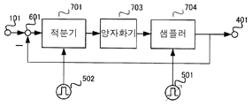
본 발명의 한 실시형태로서, 입력 신호를 입력하는 입력부와, 상기 입력부가 출력하는 신호를 적분하는 적분기와, 상기 적분기가 출력하는 신호를 양자화하는 양자화기와, 주기가 가변인 클럭 신호에 따라 상기 양자화기의 출력을 샘플링하는 샘플러를 가지고, 상기 입력부는, 입력 신호로부터 상기 샘플러의 출력을 감산처리하여 출력하는 감산기를 가지는 데이터 변환기를 제공한다.According to one embodiment of the present invention, there is provided a signal processing apparatus including an input unit for inputting an input signal, an integrator for integrating a signal output from the input unit, a quantizer for quantizing a signal output from the integrator, And a subtracter for subtracting the output of the sampler from the input signal and outputting the subtracted output.
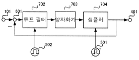
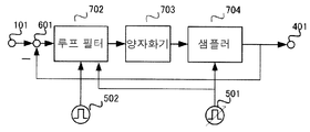
본 발명의 한 실시형태로서, 입력 신호를 입력하는 입력부와, 상기 입력부가 출력하는 신호가 입력되는 루프 필터와, 상기 루프 필터가 출력하는 신호를 양자화하는 양자화기와, 주기가 가변인 클럭 신호에 따라 상기 양자화기의 출력을 샘플링하는 샘플러를 가지고, 상기 입력부는, 입력 신호로부터 상기 샘플러의 출력을 감산처리하여 출력하는 감산기를 가지는 데이터 변환기를 제공한다.According to one embodiment of the present invention, there is provided a signal processing apparatus including an input unit for inputting an input signal, a loop filter for inputting a signal to be output from the input unit, a quantizer for quantizing a signal output from the loop filter, And a sampler for sampling the output of the quantizer, wherein the input unit includes a subtractor for subtracting the output of the sampler from the input signal and outputting the subtractor.
본 발명의 한 실시형태로서, 클럭 신호를 입력하는 클럭 신호 입력부와, 입력 신호를 입력하는 입력부와, 상기 클럭 신호 입력부에 입력되는 클럭 신호에 따라 상기 입력부에 입력된 입력 신호의 샘플링을 하는 샘플링부와, 상기 샘플링의 주기에 따라 신호처리를 하여, 출력 신호를 출력하는 신호 처리부와, 상기 신호 처리부가 출력하는 출력 신호에 따라 액추에이터를 구동하는 드라이버를 가지고, 상기 클럭 신호 입력부에 입력되는 클럭 신호의 주기가 길어지면, 상기 신호 처리부가 출력하는 출력 신호를 작게 하는 데이터 변환기를 제공한다.According to one embodiment of the present invention, there is provided a clock signal processing apparatus including a clock signal input unit for inputting a clock signal, an input unit for inputting an input signal, a sampling unit for sampling an input signal input to the input unit in accordance with a clock signal input to the clock signal input unit, And a driver for driving an actuator according to an output signal outputted from the signal processing unit, wherein the clock signal input to the clock signal input unit is a clock signal input to the clock signal input unit, And provides a data converter that reduces the output signal output by the signal processing unit when the period becomes longer.
본 발명에 의하면, 아날로그-디지털 변환기, 디지털-아날로그 변환기에 이용하는 클럭 신호의 주기를 동적으로 변경하고, 그 스펙트럼을 확산시킴과 함께, 변환 정밀도를 열화시키는 일 없이, 아날로그-디지털 변환기, 디지털-아날로그 변환기의 내부신호 및 이것에 의해 복사되는 신호를 대폭 저감시킬 수 있다. 이것에 의해, 더 높은 주파수의 클럭 신호를 사용하는 것도 가능해지며, 변환 정밀도를 더욱 고정밀화할 수도 있다.According to the present invention, it is possible to dynamically change the period of the clock signal used in the analog-to-digital converter and the digital-analog converter, spread the spectrum, The internal signal of the converter and the signal copied thereby can be greatly reduced. As a result, it is possible to use a clock signal of a higher frequency, and the conversion accuracy can be further increased.
도 1은 디지털-아날로그 변환기의 구성도.
도 2는 클럭 변조를 이용하는 디지털-아날로그 변환기의 구성도.
도 3는 본 발명의 제1 실시형태에 관련된 데이터 변환기의 구성도.
도 4는 본 발명의 제2 실시형태에 관련된 데이터 변환기의 구성도.
도 5는 본 발명의 제3 실시형태에 관련된 데이터 변환기의 구성도.
도 6은 본 발명의 제4 실시형태에 관련된 데이터 변환기의 구성도.
도 7은 본 발명의 제5 실시형태에 관련된 데이터 변환기의 구성도.
도 8a는 본 발명의 제6 실시형태에 관련된 데이터 변환기의 구성도.
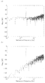
도 8b의 (a)는 종래기술에서의 데이터 변환기의 출력 스펙트럼을 나타내는 그래프, (b)는 본 발명의 제6 실시형태에서의 데이터 변환기의 출력 스펙트럼을 나타내는 그래프.
도 8c의 (a)는 종래기술에서의 데이터 변환기의 광대역 출력 스펙트럼을 나타내는 그래프, (b)는 본 발명의 제6 실시형태에서의 데이터 변환기의 광대역 출력 스펙트럼을 나타내는 그래프.
도 9는 본 발명의 제7 실시형태에 관련된 데이터 변환기의 구성도.
도 10은 본 발명의 제8 실시형태에 관련된 데이터 변환기의 구성도.
도 11은 본 발명의 제9 실시형태에 관련된 데이터 변환기의 구성도.
도 12는 본 발명의 제10 실시형태에 관련된 데이터 변환기의 구성도.
도 13은 본 발명의 제10 실시형태에 관련된 데이터 변환기에 이용하는 미스매치 셰이퍼의 구성예를 나타내는 도.
도 14는 본 발명의 제11 실시형태에 관련된 데이터 변환기의 구성도.
도 15는 본 발명의 제12 실시형태에 관련된 데이터 변환기의 구성도.1 is a configuration diagram of a digital-analog converter;
2 is a block diagram of a digital-to-analog converter using clock modulation.
3 is a configuration diagram of a data converter according to a first embodiment of the present invention;
4 is a configuration diagram of a data converter according to a second embodiment of the present invention;
5 is a configuration diagram of a data converter according to a third embodiment of the present invention;
6 is a configuration diagram of a data converter according to a fourth embodiment of the present invention;
7 is a configuration diagram of a data converter according to a fifth embodiment of the present invention;
8A is a configuration diagram of a data converter according to a sixth embodiment of the present invention;
FIG. 8A is a graph showing the output spectrum of the data converter in the prior art, and FIG. 8B is a graph showing the output spectrum of the data converter in the sixth embodiment of the present invention. FIG.
FIG. 8C is a graph showing a wideband output spectrum of the data converter in the prior art, and FIG. 8B is a graph showing the broadband output spectrum of the data converter in the sixth embodiment of the present invention.
9 is a configuration diagram of a data converter according to a seventh embodiment of the present invention;
10 is a configuration diagram of a data converter according to an eighth embodiment of the present invention;
11 is a configuration diagram of a data converter according to a ninth embodiment of the present invention.
12 is a configuration diagram of a data converter according to a tenth embodiment of the present invention;
13 is a diagram showing a configuration example of a mismatch shaper used in a data converter according to a tenth embodiment of the present invention;
14 is a configuration diagram of a data converter according to an eleventh embodiment of the present invention;
15 is a configuration diagram of a data converter according to a twelfth embodiment of the present invention;
이하, 도면을 참조하면서 본 발명을 실시하기 위한 형태를 몇 가지 실시형태를 이용하여 상세하게 설명한다. 또한, 본 발명은 이러한 실시형태에 한정되지 않으며, 그 요지를 일탈하지 않는 범위에서 여러 가지의 변형을 실시하는 것이 가능하다.Hereinafter, embodiments for carrying out the present invention will be described in detail with reference to the accompanying drawings. The present invention is not limited to these embodiments, and various modifications can be made without departing from the gist of the invention.
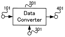
도 3을 참조하여, 본 발명의 제1 실시형태에 대해 설명한다.A first embodiment of the present invention will be described with reference to Fig.
입력수단(101)에 입력된 입력 신호를 클럭 신호 입력수단(301)에 입력되는 클럭 신호에 동기하여 데이터 변환기(201) 내의 샘플링수단에 의해 샘플링하고, 이 샘플링 주기에 따라 신호처리수단에 의해 신호처리를 한다. 디지털 신호를 아날로그로 변환하는 경우, 샘플링 주기가 변화하면, 출력 신호가 변화하는 타이밍이, 클럭 주파수의 주기의 변동에 따라 변화한다. 예컨대, 클럭 주기가 긴 경우에는, 출력 신호의 펄스폭은 넓어져, 출력 신호가 커진 것과 등가가 된다. 이것에 의해, 출력 신호의 스펙트럼이 확산되어, 특정 주파수에서의 스펙트럼의 피크치를 저감시키는 것이 가능해진다.The input signal inputted to the input means 101 is sampled by the sampling means in the
그러나, 일반적으로 출력의 타이밍을 변화시키는 것에 의해, 신호성분의 스펙트럼도 확산하게 되어, 원래 특성과 다른 신호를 출력하게 되어 버린다. 이 때문에, 신호의 정밀도가 현저하게 손상되어 버린다.However, by changing the timing of the output in general, the spectrum of the signal component is also diffused, and a signal different from the original characteristic is output. Therefore, the accuracy of the signal is remarkably impaired.
본 실시형태에서는, 이 영향을 저감시키기 위해, 내부의 신호처리로 출력하는 신호를 작게 하도록 수정하는 것이 특징 중 하나이다. 이와 같이 함으로써, 클럭 신호의 주기의 영향을 저감시켜, 고정밀도 변환을 실현하는 것이 가능해져, 변환출력을 출력수단(401)에서 얻을 수 있다.In this embodiment, in order to reduce the influence, it is one of the features that the signal output by the internal signal processing is modified so as to be small. In this way, the influence of the period of the clock signal can be reduced, high-precision conversion can be realized, and the output of the conversion can be obtained by the output means 401.
종래의 방법에서는, 클럭 주기를 동적으로 변화시킨 경우, 신호를 지터가 있는 클럭 신호로 샘플링한 것과 등가가 되어, 신호 대 잡음비(SNR)가 대폭 열화되게 된다.In the conventional method, when the clock period is changed dynamically, the signal is equivalent to sampling with a jittered clock signal, and the signal-to-noise ratio (SNR) is greatly degraded.
본 실시형태에서 데이터 변환기(201)로서, 아날로그-디지털 변환기, 디지털-아날로그 변환기, 오버샘플링형 아날로그-디지털 변환기, 오버샘플링형 오버샘플링형, ΔΣ 변조기, ΔΣ형 디지털-아날로그 변환기, ΔΣ형 아날로그-디지털 변환기 등 여러 가지 변환기를 구성하는 것이 가능하다.In the present embodiment, as the
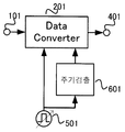
도 4를 참조하여, 본 발명의 제2 실시형태에 대해 설명한다. 본 실형태에서는, 주기가 동적으로 변경되는 클럭 신호 생성기(501)를 데이터 변환기(201)의 클럭 입력수단(301)에 접속하고, 클럭 신호 생성기(501)는, 주기 검출수단(601)에 접속되며, 이 주기 검출수단(601)은, 입력 클럭 신호의 주기를 검출한다. 주기 검출수단(601)의 출력은 데이터 변환기(201)에 접속되고, 데이터 변환기(201)의 신호 처리부는, 주기 검출수단(601)의 출력에 따라 신호처리를 한다.A second embodiment of the present invention will be described with reference to Fig. The
이것에 의해, 출력 신호의 정밀도를 열화시키는 일 없이, 출력 신호의 스펙트럼을 확산하여, 특정 주파수에서의 스펙트럼의 피크치를 저감시키는 것이 가능해진다.This makes it possible to diffuse the spectrum of the output signal without degrading the accuracy of the output signal, thereby reducing the peak value of the spectrum at a specific frequency.
도 5를 참조하여, 본 발명의 제3 실시형태에 대해 설명한다. 본 실시형태는, 주기가 동적으로 변화하는 클럭 생성회로를 이용한다. 도 5에 나타낸 바와 같이, 클럭생성부는, 클럭 신호 생성수단(502)과 분주수단(503)과 분주비 생성수단(504)에 의해 구성된다. 분주비 생성수단(504)의 신호에 따라 분주수단(503)은, 클럭 신호 생성수단(502)을 분주한다. 분주비 생성수단(504)은, 분주비를 동적으로 변화시킬 수 있다. 이것에 의해, 분주수단(504)으로부터 주기가 동적으로 변화하는 신호를 출력하고, 분주비 생성수단(504)으로부터 분주수단(504)의 출력 주기에 따른 신호를 출력할 수 있다. 이러한 신호를, 데이터 변환기(201)에 접속하는 것에 의해, 데이터 변환기(201)로 클럭 주기에 따른 신호처리를 하는 것이 가능해진다.A third embodiment of the present invention will be described with reference to Fig. In the present embodiment, a clock generation circuit in which the period changes dynamically is used. As shown in Fig. 5, the clock generating section is constituted by a clock signal generating means 502, a frequency dividing means 503 and a frequency dividing ratio generating means 504. The frequency dividing means 503 divides the clock signal generating means 502 in accordance with the signal of the frequency dividing ratio generating means 504. The division ratio generating means 504 can change the division ratio dynamically. Thereby, a signal whose period changes dynamically is output from the frequency dividing means 504, and a signal corresponding to the output period of the frequency dividing means 504 can be output from the frequency dividing ratio generating means 504. By connecting such a signal to the
이것에 의해, 출력 신호의 정밀도를 열화시키는 일 없이, 출력 신호의 스펙트럼을 확산하여, 특정 주파수에서의 스펙트럼의 피크치를 저감시키는 것이 가능해진다.This makes it possible to diffuse the spectrum of the output signal without degrading the accuracy of the output signal, thereby reducing the peak value of the spectrum at a specific frequency.
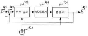
도 6을 참조하여, 본 발명의 제4 실시형태에 대해 설명한다. 본 실시형태에서는 데이터 변환기(201)를, 적분수단(701), 감산수단(601), 양자화수단(703), 샘플링수단(704)에 의해 구성한다. 샘플링수단(704)의 출력을 입력 신호로부터 감산수단(601)으로 감산하고, 이 신호를 적분수단(701)으로 적분하여, 양자화수단(703)으로 양자화한다. 양자화된 신호는, 샘플링수단(704)으로 샘플링한다. 이 양자화와 샘플링은, 컴퍼레이터 회로 등의 동일한 수단으로 구성하는 것도 가능하다.A fourth embodiment of the present invention will be described with reference to Fig. In the present embodiment, the
샘플링수단(704)은, 가변 주기 클럭 신호 생성기(501)의 클럭 신호에 따라 샘플링을 한다. 이 때문에, 클럭 신호의 주기가 길어진 경우에는, 출력 신호를 유지하는 시간도 길어진다. 한편, 입력 신호로부터 감산수단(601)으로 샘플링수단(704)의 출력을 감산한 신호는 적분수단(701)으로 적분된다. 이 때문에, 감산수단(601)의 출력 신호는 가변 주기 클럭 신호 생성기(501)의 주기에 따른 시간 적분을 하게 된다.The sampling means 704 samples according to the clock signal of the variable period
따라서, 이와 같이 구성함으로써, 클럭 신호의 주기에 따른 신호처리가 가능해진다.Thus, by such a configuration, signal processing according to the period of the clock signal becomes possible.
바꾸어 말하면, 샘플링 기간이 변동하는 샘플링수단(704)의 출력이, 피드백되게 된다. 이것에 의해, 종래의 방법에서는 클럭 주기가 변화한 것에 의해 출력 신호의 정밀도가 열화되지만, 그 영향을 대폭 저감하는 것이 가능해진다.In other words, the output of the sampling means 704 whose sampling period fluctuates is fed back. Thus, in the conventional method, the precision of the output signal is deteriorated due to the change of the clock period, but the influence thereof can be greatly reduced.
이것에 의해, 출력 신호의 정밀도를 열화시키는 일 없이, 출력 신호의 스펙트럼을 확산하여, 특정 주파수에서의 스펙트럼의 피크치를 저감시키는 것이 가능해진다.This makes it possible to diffuse the spectrum of the output signal without degrading the accuracy of the output signal, thereby reducing the peak value of the spectrum at a specific frequency.
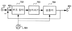
도 7을 참조하여, 본 발명의 제5 실시형태에 대해 설명한다. 본 실시형태는 제4 실시형태에서의 적분기를 루프 필터로 바꾼 점이 다르다.A fifth embodiment of the present invention will be described with reference to Fig. The present embodiment differs from the fourth embodiment in that the integrator is replaced by a loop filter.
일반적으로, ΔΣ 변조기에서는, 루프 내에 이용하는 적분기의 차수를 올리는 것에 의해, 대역 내의 잡음을 저감시킬 수 있어, 변환 정밀도를 향상시킬 수 있다. 본 발명에서도 루프 필터의 차수를 올리는 것에 의해, 변환 정밀도의 향상을 도모하는 것이 가능해진다. 또한, 루프 필터에 공진기를 이용함으로써, 특정 주파수에서의 잡음을 저감시키는 것도 가능하여, 이른바 밴드패스 변환 특성을 실현할 수 있다.In general, in the ?? modulator, by raising the order of the integrator used in the loop, the noise in the band can be reduced, and the conversion precision can be improved. In the present invention, it is also possible to improve the conversion accuracy by increasing the degree of the loop filter. Further, by using a resonator in the loop filter, noise at a specific frequency can be reduced, and so-called band pass conversion characteristics can be realized.
도 8a를 참조하여, 본 발명의 제6 실시형태에 대해 더욱 상세하게 설명한다. 플립플롭(705) 및 가산수단(602)에 의해 적분기를 구성하고, 적분기 출력을 계수수단(603)으로 계수배한다. 본 실시형태에서는 적분기를 2단 직렬접속하고 있지만, 3단 이상 접속하는 것도 가능하다. 최후단의 적분기 출력을 양자화수단(703)으로 양자화하고, 플립플롭(705)으로 샘플링한다. 이 플립플롭의 클럭은, 주기가 동적으로 변경되는 클럭 신호 생성기(501)로부터의 신호에 따라, 샘플링 타이밍을 결정하고 있다. 한편, 적분기를 구성하는 플립플롭(705)에는 고정 주기의 클럭 신호를 공급하고 있다.A sixth embodiment of the present invention will be described in more detail with reference to Fig. The flip-
이 때, 클럭 신호 생성기(501)의 주기를 클럭 신호 생성기(502)의 클럭 주기보다 짧게 해 둠으로써, 클럭 신호 생성기(501)의 주기 변동에 따른 적분기 출력을 얻을 수 있어, 클럭 신호의 주기에 따른 신호처리가 가능해진다.At this time, by setting the period of the
이것에 의해, 종래의 방법에서는 클럭 주기가 변화한 것에 의해 출력 신호의 정밀도가 열화하지만, 그 영향을 대폭 저감시키는 것이 가능해진다.As a result, in the conventional method, the precision of the output signal deteriorates due to the change of the clock period, but the influence thereof can be greatly reduced.
특히, 클럭 신호 생성기(501)의 주기와 클럭 신호 생성기(502)의 주기를 정수비로 함으로써 오차 없이 신호 생성기(501)의 주기에 따른 처리가 가능해진다.Particularly, by setting the period of the
도 8b의 (a)는 종래기술을 이용한 경우에서의 출력 스펙트럼을 나타내고, 도 8b의 (b)는 본 실시형태에서의 출력 스펙트럼을 나타낸다. 이 그래프들에서 알 수 있는 바와 같이, 가변 클럭을 이용한 종래수법에서는 저역의 잡음이 대폭 상승하고 있지만, 본 실시형태를 이용하는 경우 출력 신호의 열화는 없다.FIG. 8B shows the output spectrum in the case of using the conventional technique, and FIG. 8B shows the output spectrum in the present embodiment. As can be seen from these graphs, in the conventional method using a variable clock, the noise of the low frequency band is considerably increased. However, when the present embodiment is used, there is no deterioration of the output signal.
도 8c에 광대역의 출력 스펙트럼을 나타낸다. 도 8c의 (a)는 종래기술에서의 데이터 변환기의 광대역 출력 스펙트럼을 나타내고, 도 8c의 (b)는 본 실시형태에서의 데이터 변환기의 광대역 출력 스펙트럼을 나타낸다. 본 실시형태를 이용하는 것에 의해, 스펙트럼의 피크 레벨을 대폭 저감하는 것이 가능해지는 것을 알 수 있다.FIG. 8C shows a wideband output spectrum. FIG. 8C shows the wideband output spectrum of the data converter in the prior art, and FIG. 8B shows the broadband output spectrum of the data converter in the present embodiment. It can be seen that the use of this embodiment makes it possible to drastically reduce the peak level of the spectrum.
도 9를 참조하여, 본 발명의 제7 실시형태에 대해 상세하게 설명한다. 본 실시형태는, 루프필터수단(702)에도 가변 주기의 클럭 신호 생성수단(501)을 접속하고 있다는 점이, 도 7에 나타낸 제5 실시형태와는 다르다. 루프필터수단(702)에서는, 가변 주기의 클럭 신호 생성수단(501) 및 고정 주기의 클럭 신호 생성수단(502)으로부터의 2개의 클럭 신호로부터 가변 주기의 클럭 신호 생성수단(501)의 주기를 검출하고, 이 주기에 따라 루프 필터의 계수를 변경하는 것을 특징으로 한다.A seventh embodiment of the present invention will be described in detail with reference to Fig. This embodiment is different from the fifth embodiment shown in Fig. 7 in that the loop filter means 702 is also connected to the clock signal generating means 501 of variable period. The loop filter means 702 detects the period of the variable-period clock signal generation means 501 from the two clock signals from the variable-period clock signal generation means 501 and the fixed-period clock signal generation means 502 And the coefficient of the loop filter is changed according to this period.
이와 같이 구성하는 것에 의해, 가변 주기의 클럭 신호 생성수단(501)으로부터의 클럭 주기에 대응한 루프 필터 출력을 얻는 것이 가능해진다. 도 7에 나타낸 제5 실시형태에서는, 가변 주기의 클럭 신호 생성수단(501)의 주기보다 고정 주기의 클럭 신호 생성수단(501)의 주기를 짧게 할 필요가 있지만, 본 실시형태에서는 루프 필터의 연산을, 가변 주기의 클럭 신호 생성수단(501)의 주기로 실시하는 것이 가능해진다.With this configuration, it is possible to obtain the loop filter output corresponding to the clock period from the clock signal generating means 501 of variable period. In the fifth embodiment shown in Fig. 7, it is necessary to shorten the period of the clock signal generating means 501 of fixed period to the period of the variable-period clock signal generating means 501. In this embodiment, Can be performed in the cycle of the clock signal generating means 501 of the variable period.
이것에 의해, 루프필터수단(702)의 처리 주기를 길게 설정하는 것이 가능해져, 연산 스피드에 대한 요구를 완화할 수 있다. 또한, 이것에 의해 소비전력의 삭감도 가능해진다.As a result, it is possible to set the processing period of the loop filter means 702 to be long, and it is possible to relax the demand for the operation speed. In addition, the power consumption can be reduced by this.
도 10을 참조하여, 본 발명의 제8 실시형태에 대해 상세하게 설명한다.The eighth embodiment of the present invention will be described in detail with reference to Fig.
플립플롭(705) 및 가산수단(602)에 의해 적분기를 구성하고, 적분기 출력을 가변계수수단(604)으로 계수배한다. 본 실시형태에서는 적분기를 2단 직렬접속하고 있지만, 3단 이상 접속하는 것도 가능하다. 최후단의 적분기 출력을 양자화수단(703)으로 양자화하고, 플립플롭(705)으로 샘플링한다.The flip-
본 실시형태에서는, 적분기를 구성하는 플립플롭 및 양자화기에 후치된 플립플롭 모두 분주기(503)에 접속되어 있다. 분주기(503)는, 고정 주기의 클럭 신호 생성수단(502)을 분주비 생성수단(504)의 분주비에 따라 분주하여, 가변 주기의 클럭 신호를 생성하고 있다. 따라서, 상기 플립플롭은 모두 가변 주기의 클럭 신호에 의해 구동되고 있다.In the present embodiment, both the flip-flop constituting the integrator and the flip-flop posterior to the quantizer are connected to the
가변계수수단(604)의 계수는 분주비 생성수단(504)에 따라 변경된다. 이것에 의해, 분주기(503)로부터의 가변 주기의 클럭 주기에 따라서, 적분기로 구성되어 있는 루프 필터의 특성을 가변하는 것이 가능해져, 클럭 주기가 변화하는 것에 따른 특성의 열화를 대폭 저감하는 것이 가능해진다.The coefficient of the variable coefficient means 604 is changed in accordance with the frequency division ratio generation means 504. Thus, it is possible to vary the characteristics of the loop filter constituted by the integrator in accordance with the clock period of the variable period from the
도 11을 참조하여, 본 발명의 제9 실시형태에 대해 설명한다.A ninth embodiment of the present invention will be described with reference to Fig.
본 실시형태에서는 제1 실시형태의 데이터 변환기의 후단으로서, 드라이버 수단(801)을 접속하고 있다. 드라이버 수단(801)은, 드라이버 수단(801)에 접속되는 액추에이터 등을 구동할 수 있는 특성을 가지고 있다.In the present embodiment, a driver means 801 is connected as the rear end of the data converter of the first embodiment. The driver means 801 has a characteristic capable of driving an actuator or the like connected to the driver means 801. [
예컨대, 전압 구동하는 경우에는, 충분히 낮은 출력 임피던스의 드라이버 회로를 가지도록 한다. 이것에 의해, 데이터 변환 수단(201)에서 생성된 신호를 액추에이터 등에 정확하게 전달하는 것이 가능해져, 고정밀도 변환이 가능해진다.For example, in the case of voltage driving, a driver circuit with a sufficiently low output impedance is provided. Thus, it is possible to accurately transmit the signal generated by the data conversion means 201 to the actuator or the like, and high-precision conversion becomes possible.
또한, 드라이버 수단(801)에서는 입력 신호를 온도계 코드로 변환하여 출력하는 것도 가능하다. 온도계 코드로 변환함으로써, 드라이버 회로 및 액추에이터의 특성편차를 저감하는 것이 가능해진다.In addition, the driver means 801 can convert the input signal into a thermometer code and output it. By converting to a thermometer code, it is possible to reduce the characteristic deviation of the driver circuit and the actuator.
그리고, 드라이버 수단(801)에서는, 입력 신호를, 각 액추에이터를 +1, 0, -1과 같이 3상태로 구동하는 3치 코드로 변환하여 출력하는 것도 가능하다. 3치 코드로 변환함으로써, 저출력시에는 액추에이터를 0구동, 즉 구동하지 않는 것이 가능해져, 소비전력의 대폭적인 저감이 가능해진다.In the driver means 801, it is also possible to convert the input signal into a ternary code for driving each actuator in three states, such as +1, 0, and -1, and output it. By converting to a ternary code, it becomes possible to drive the actuator at zero, that is, not to drive at low output, and it is possible to drastically reduce power consumption.
본 실시형태에서는 드라이버 수단(801)을 데이터 변환 수단(201)에 접속하고 있지만, 상기한 어느 한 실시형태의 출력에 접속하여, 성능을 향상시키는 것이 가능하다.In the present embodiment, the driver means 801 is connected to the data conversion means 201, but it is possible to improve the performance by connecting to the output of any of the above embodiments.
도 12를 참조하여, 본 발명의 제10 실시형태에 대해 설명한다.A tenth embodiment of the present invention will be described with reference to Fig.
본 실시형태에서는, 제9 실시형태의 데이터 변환 수단(201)과 드라이버 수단(801) 사이에, 미스매치 셰이퍼 수단(901)을 삽입하고 있다.In the present embodiment, mismatch shaper means 901 is inserted between the data conversion means 201 and the driver means 801 of the ninth embodiment.
제9 실시형태에서는, 출력을 온도계 코드나 3치 코드로 변환함으로써 드라이버 회로 및 액추에이터 등의 편차를 작게 하는 것은 가능해졌지만, 이에 따른 변환 정밀도의 열화에 의해 충분한 성능을 얻을 수 없는 경우가 있다. 본 실시형태에서는 이 편차의 영향에 대해, 특성 주파수에서의 잡음을 미스매치 셰이퍼 수단(901)에 의해 저감시키는 것이 가능해진다.In the ninth embodiment, it is possible to reduce the deviation of the driver circuit and the actuator by converting the output into the thermometer code or the ternary code. However, there is a case that satisfactory performance can not be obtained due to the deterioration of the conversion accuracy. In the present embodiment, it is possible to reduce the noise at the characteristic frequency by the mismatch shaper means 901 with respect to the influence of this deviation.
도 13에 미스매치 셰이퍼 수단(901)의 상세한 구성예를 나타낸다.Fig. 13 shows a detailed configuration example of the mismatch shaper means 901. Fig.
미스매치 셰이퍼 수단(901)은 선택 수단(902), 필터수단(903)에 의해 구성되며, 입력 신호로 지정된 값에 대응한 액추에이터 등의 선택 대상을 선택한다. 드라이버 수단(801)이 3치 코드를 이용하는 경우에는, 액추에이터를 +1, 0, -1과 같은 3상태 중 어느 하나의 신호를 출력한다. 이 선택은 필터수단(903)의 출력에 따라 실시한다. 이 필터수단은 통상 적분기를 종속접속한 필터로 구성된다.The mismatch shaper means 901 is constituted by a selection means 902 and a filter means 903 and selects an object to be selected such as an actuator corresponding to a value specified by an input signal. When the driver means 801 uses a ternary code, the actuator outputs any one of the three states of +1, 0, and -1. This selection is made in accordance with the output of the filter means 903. This filter means usually consists of a filter cascade-connected to an integrator.
또한, 이 필터수단은 통상 적분기를 종속접속한 필터로 구성되지만, 미스매치 셰이퍼 수단(901)의 주기에 따라 처리함으로써 특성을 더욱 향상시키는 것이 가능하다. 제5 내지 제8 실시형태에서 나타낸 루프 필터와 동일하게 필터수단(903)을 구성하는 것에 의해, 출력 기간에 따른 처리가 가능해지고, 출력 시간을 고려한 미스매치 셰이핑이 가능해진다.The filter means is usually constituted by a filter cascade-connected to an integrator, but it is possible to further improve the characteristics by processing in accordance with the cycle of the mismatch shaper means 901. By configuring the filter means 903 in the same manner as the loop filter shown in the fifth to eighth embodiments, processing according to the output period becomes possible, and mismatch shaping considering the output time becomes possible.
도 14를 참조하여, 본 발명의 제11 실시형태에 대해 설명한다.The eleventh embodiment of the present invention will be described with reference to Fig.
본 실시형태에서는 액추에이터에 스피커를 이용하고 있다. 이와 같이 구성하는 것에 의해, 디지털 신호를 고정밀도로 직접 음압으로 변환하는 것이 가능해진다.In this embodiment, a speaker is used for the actuator. With this configuration, it becomes possible to directly convert the digital signal into a sound pressure with high accuracy.
이것에 의해, 출력 신호의 정밀도를 열화시키는 일 없이, 출력 신호의 스펙트럼을 확산하여, 특정 주파수에서의 스펙트럼의 피크치를 저감하는 것이 가능해진다.This makes it possible to diffuse the spectrum of the output signal without deteriorating the accuracy of the output signal, thereby reducing the peak value of the spectrum at a specific frequency.
도 15를 참조하여, 본 발명의 제12 실시형태에 대해 설명한다.A twelfth embodiment of the present invention will be described with reference to Fig.
본 실시형태에서는 액추에이터에 디지털-아날로그 변환 수단(1002)을 이용하고 있다. 이와 같이 구성하는 것에 의해, 디지털 신호를 고정밀도로 아날로그 신호로 변환하는 것이 가능해진다.In the present embodiment, the digital-
이것에 의해, 출력 신호의 정밀도를 열화시키는 일 없이, 출력 신호의 스펙트럼을 확산하여, 특정 주파수에서의 스펙트럼의 피크치를 저감하는 것이 가능해진다.This makes it possible to diffuse the spectrum of the output signal without deteriorating the accuracy of the output signal, thereby reducing the peak value of the spectrum at a specific frequency.
Claims (15)
입력 신호를 입력하는 입력부와,
상기 클럭 신호 입력부에 입력되는 클럭 신호에 따라, 상기 입력부에 입력된 입력 신호의 샘플링을 하는 샘플링부와,
상기 샘플링의 주기에 따라 신호처리를 하여, 출력 신호를 출력하는 신호 처리부를 가지고,
상기 클럭 신호 입력부에 입력되는 클럭 신호의 주기가 길어지면, 상기 신호 처리부가 출력하는 출력 신호를 작게 하는 데이터 변환기.A clock signal input unit for inputting a clock signal,
An input unit for inputting an input signal,
A sampling unit for sampling an input signal input to the input unit according to a clock signal input to the clock signal input unit,
And a signal processing unit for performing signal processing according to the sampling period and outputting an output signal,
Wherein the clock signal input unit is configured to reduce an output signal output from the signal processing unit when a period of a clock signal input to the clock signal input unit becomes longer.
입력 신호를 입력하는 입력부와,
상기 클럭 신호 입력부에 입력된 클럭 신호의 주기를 검출하는 주기 검출부와,
상기 입력부에 입력된 입력 신호를 상기 주기 검출부에 의해 검출된 클럭 신호의 주기에 따라 신호처리를 하여, 출력 신호를 출력하는 신호 처리부
를 가지는 데이터 변환기.A clock signal input unit for inputting a clock signal whose period changes dynamically,
An input unit for inputting an input signal,
A cycle detector for detecting a cycle of the clock signal input to the clock signal input unit,
A signal processing section for performing signal processing on the input signal inputted to the input section according to the period of the clock signal detected by the period detecting section,
/ RTI >
상기 데이터 변환기는, 출력 신호의 스펙트럼을 확산하여, 특정 주파수에서의 스펙트럼의 피크치를 저감시키는 데이터 변환기.3. The method of claim 2,
Wherein the data converter diffuses the spectrum of the output signal to reduce the peak value of the spectrum at a specific frequency.
상기 클럭 신호 입력부는,
분주비를 동적으로 변화시키는 분주비 생성기와,
상기 분주비 생성기에 의해 변화된 분주비에 따라 클럭 신호를 분주하여 입력하는 분주기
를 가지고,
상기 주기 검출부는, 상기 분주비 생성기에 의해 변화된 분주비에 의해 클럭 신호의 주기를 검출하는 데이터 변환기.The method according to claim 2 or 3,
Wherein the clock signal input unit comprises:
A dividing ratio generator for dynamically changing the dividing ratio,
And a frequency divider for dividing and inputting the clock signal according to the division ratio changed by the division ratio generator,
Lt; / RTI &
Wherein the period detecting section detects the period of the clock signal by the frequency division ratio changed by the frequency division ratio generator.
상기 입력부가 출력하는 신호를 적분하는 적분기와,
상기 적분기가 출력하는 신호를 양자화하는 양자화기와,
주기가 가변인 클럭 신호에 따라 상기 양자화기의 출력을 샘플링하는 샘플러
를 가지고,
상기 입력부는,
입력 신호로부터 상기 샘플러의 출력을 감산처리하여 출력하는 감산기를 가지는 데이터 변환기.An input unit for inputting an input signal,
An integrator for integrating a signal output from the input unit,
A quantizer for quantizing a signal output by the integrator,
A sampler for sampling the output of the quantizer according to a clock signal whose cycle is variable;
Lt; / RTI &
Wherein the input unit comprises:
And a subtractor for subtracting the output of the sampler from the input signal and outputting the result.
상기 적분기에 공급되는 클럭 신호의 주기가, 상기 샘플러가 상기 양자화기의 출력을 샘플링할 때 따르는 클럭 신호의 주기보다 작은 데이터 변환기.6. The method of claim 5,
Wherein the period of the clock signal supplied to the integrator is less than the period of the clock signal that follows when the sampler samples the output of the quantizer.
상기 적분기에 공급되는 클럭 신호의 주기와 상기 샘플러가 상기 양자화기의 출력을 샘플링할 때 따르는 클럭 신호의 주기가 정수비인 데이터 변환기.The method according to claim 5 or 6,
Wherein the period of the clock signal supplied to the integrator and the period of the clock signal when the sampler samples the output of the quantizer are integer constants.
상기 입력부가 출력하는 신호가 입력되는 루프 필터와,
상기 루프 필터가 출력하는 신호를 양자화하는 양자화기와,
주기가 가변인 클럭 신호에 따라 상기 양자화기의 출력을 샘플링하는 샘플러
를 가지고,
상기 입력부는,
입력 신호로부터 상기 샘플러의 출력을 감산처리하여 출력하는 감산기를 가지는 데이터 변환기.An input unit for inputting an input signal,
A loop filter to which a signal output by the input unit is inputted,
A quantizer for quantizing a signal output from the loop filter,
A sampler for sampling the output of the quantizer according to a clock signal whose cycle is variable;
Lt; / RTI &
Wherein the input unit comprises:
And a subtractor for subtracting the output of the sampler from the input signal and outputting the result.
상기 루프 필터는 공진기인 데이터 변환기.9. The method of claim 8,
Wherein the loop filter is a resonator.
상기 루프 필터는, 상기 루프 필터에 공급되는 클럭 신호의 주기를 검출하여 상기 루프 필터의 계수를 변경하는 데이터 변환기.9. The method of claim 8,
Wherein the loop filter detects a period of a clock signal supplied to the loop filter to change a coefficient of the loop filter.
분주비를 동적으로 변화시키는 분주비 생성기와,
상기 분주비 생성기에 의해 변화된 분주비에 따라 클럭 신호를 분주하여 입력하는 분주기
를 가지고,
상기 샘플러가 상기 양자화기의 출력을 샘플링할 때 따르는 클럭 신호는, 상기 분주기의 출력 신호이며,
상기 분주기의 출력 신호가 상기 루프 필터에도 공급되는 데이터 변환기.11. The method of claim 10,
A dividing ratio generator for dynamically changing the dividing ratio,
And a frequency divider for dividing and inputting the clock signal according to the division ratio changed by the division ratio generator,
Lt; / RTI &
Wherein the clock signal that follows when the sampler samples the output of the quantizer is an output signal of the divider,
And the output signal of the frequency divider is supplied to the loop filter.
입력 신호를 입력하는 입력부와,
상기 클럭 신호 입력부에 입력되는 클럭 신호에 따라, 상기 입력부에 입력된 입력 신호의 샘플링을 하는 샘플링부와,
상기 샘플링의 주기에 따라 신호처리를 하여, 출력 신호를 출력하는 신호 처리부와,
상기 신호 처리부가 출력하는 출력 신호에 따라 액추에이터를 구동하는 드라이버
를 가지고,
상기 클럭 신호 입력부에 입력되는 클럭 신호의 주기가 길어지면, 상기 신호 처리부가 출력하는 출력 신호를 작게 하는 데이터 변환기.A clock signal input unit for inputting a clock signal,
An input unit for inputting an input signal,
A sampling unit for sampling an input signal input to the input unit according to a clock signal input to the clock signal input unit,
A signal processing unit for performing signal processing according to the sampling period and outputting an output signal;
A driver for driving an actuator in accordance with an output signal outputted from the signal processing unit
Lt; / RTI &
Wherein the clock signal input unit is configured to reduce an output signal output from the signal processing unit when a period of a clock signal input to the clock signal input unit becomes longer.
상기 드라이버는, 3치 코드를 출력하여 상기 액추에이터를 구동하는 데이터 변환기.13. The method of claim 12,
And the driver outputs a ternary code to drive the actuator.
상기 신호 처리부가 출력하는 출력 신호를 입력하여 상기 드라이버에 신호를 출력하는 미스매치 셰이퍼를 가지는 데이터 변환기.The method according to claim 12 or 13,
And a mismatch shaper for inputting an output signal output from the signal processing unit and outputting a signal to the driver.
상기 액추에이터는 스피커인 데이터 변환기.15. The method according to any one of claims 12 to 14,
Wherein the actuator is a speaker.
Applications Claiming Priority (3)
| Application Number | Priority Date | Filing Date | Title |
|---|---|---|---|
| JP2012235910 | 2012-10-25 | ||
| JPJP-P-2012-235910 | 2012-10-25 | ||
| PCT/JP2013/078998 WO2014065408A1 (en) | 2012-10-25 | 2013-10-25 | Converter |
Publications (1)
| Publication Number | Publication Date |
|---|---|
| KR20150077420A true KR20150077420A (en) | 2015-07-07 |
Family
ID=50544779
Family Applications (1)
| Application Number | Title | Priority Date | Filing Date |
|---|---|---|---|
| KR1020157010459A KR20150077420A (en) | 2012-10-25 | 2013-10-25 | Converter |
Country Status (7)
| Country | Link |
|---|---|
| US (1) | US9362943B2 (en) |
| EP (1) | EP2913931A4 (en) |
| JP (1) | JP6316751B2 (en) |
| KR (1) | KR20150077420A (en) |
| CN (1) | CN104718704A (en) |
| IN (1) | IN2015DN03872A (en) |
| WO (1) | WO2014065408A1 (en) |
Families Citing this family (3)
| Publication number | Priority date | Publication date | Assignee | Title |
|---|---|---|---|---|
| CN104581589B (en) * | 2014-12-31 | 2018-01-02 | 苏州上声电子有限公司 | Channel status choosing method and device based on tri-state coding |
| US9397677B1 (en) * | 2015-11-02 | 2016-07-19 | Keysight Technologies, Inc. | Method and system for digital-to-analog converter performance measurement using equivalent-time sampler |
| CN105761691A (en) * | 2016-05-04 | 2016-07-13 | 深圳市华星光电技术有限公司 | Grid scanning line driving method, driving module and TFT-LCD panel |
Family Cites Families (12)
| Publication number | Priority date | Publication date | Assignee | Title |
|---|---|---|---|---|
| US5471209A (en) * | 1994-03-03 | 1995-11-28 | Echelon Corporation | Sigma-delta converter having a digital logic gate core |
| ATE304752T1 (en) * | 2001-10-31 | 2005-09-15 | Freescale Semiconductor Inc | INCREMENTAL DELTA ANALOG-DIGITAL CONVERTER |
| US7146144B2 (en) * | 2003-10-20 | 2006-12-05 | Northrop Grumman Corporation | Frequency agile exciter |
| JP4687510B2 (en) * | 2006-03-08 | 2011-05-25 | 日本電気株式会社 | Signal processing system and method in mobile communication terminal and mobile communication terminal using the same |
| US8116368B2 (en) * | 2006-07-27 | 2012-02-14 | National University Corporation Nagoya Institute Of Technology | PWM signal generator, PWM signal generating device, and digital amplifier |
| EP2056461A4 (en) * | 2006-08-23 | 2011-10-26 | Asahi Kasei Emd Corp | Delta-sigma modulator |
| US7619487B2 (en) * | 2007-09-14 | 2009-11-17 | Infineon Technologies Ag | Polar modulation without analog filtering |
| EP2063534B1 (en) * | 2007-11-23 | 2012-02-01 | STMicroelectronics Srl | Clock dithering process for reducing electromagnetic interference in D/A converters and apparatus for carrying out such process |
| JP2010041478A (en) * | 2008-08-06 | 2010-02-18 | Mitsubishi Electric Engineering Co Ltd | Pulse width modulation system digital/analog converter |
| JP5365437B2 (en) * | 2009-09-11 | 2013-12-11 | 株式会社リコー | Image reading apparatus and image forming apparatus |
| KR101634359B1 (en) | 2009-09-23 | 2016-06-28 | 삼성전자주식회사 | The analog-digital converter controlling gain by changing clock signal, image sensor including the same |
| US8179174B2 (en) * | 2010-06-15 | 2012-05-15 | Mstar Semiconductor, Inc. | Fast phase locking system for automatically calibrated fractional-N PLL |
-
2013
- 2013-10-25 IN IN3872DEN2015 patent/IN2015DN03872A/en unknown
- 2013-10-25 EP EP13848684.0A patent/EP2913931A4/en not_active Withdrawn
- 2013-10-25 WO PCT/JP2013/078998 patent/WO2014065408A1/en active Application Filing
- 2013-10-25 JP JP2014543364A patent/JP6316751B2/en active Active
- 2013-10-25 KR KR1020157010459A patent/KR20150077420A/en not_active Application Discontinuation
- 2013-10-25 CN CN201380053826.8A patent/CN104718704A/en active Pending
-
2015
- 2015-04-24 US US14/695,385 patent/US9362943B2/en active Active
Also Published As
| Publication number | Publication date |
|---|---|
| US20150236713A1 (en) | 2015-08-20 |
| JPWO2014065408A1 (en) | 2016-09-08 |
| CN104718704A (en) | 2015-06-17 |
| EP2913931A1 (en) | 2015-09-02 |
| IN2015DN03872A (en) | 2015-10-02 |
| EP2913931A4 (en) | 2016-08-03 |
| WO2014065408A1 (en) | 2014-05-01 |
| JP6316751B2 (en) | 2018-04-25 |
| US9362943B2 (en) | 2016-06-07 |
Similar Documents
| Publication | Publication Date | Title |
|---|---|---|
| CN106888018B (en) | Digital measurement of DAC timing mismatch error | |
| JP6421145B2 (en) | Ultra-low power dual quantizer structure for oversampling delta-sigma modulators | |
| US9716509B2 (en) | Digital measurement of DAC switching mismatch error | |
| JP3836328B2 (en) | Integrated circuit having AD converter | |
| US6426714B1 (en) | Multi-level quantizer with current mode DEM switch matrices and separate DEM decision logic for a multibit sigma delta modulator | |
| EP3182600A1 (en) | Dither injection for continuous-time mash adcs | |
| US7557744B2 (en) | PWM driver and class D amplifier using same | |
| CA2562254C (en) | A method and system for analog to digital conversion using digital pulse width modulation (pwm) | |
| KR101933575B1 (en) | Modified dynamic element matching for reduced latency in a pipeline analog to digital converter | |
| US11329660B2 (en) | VCO-based continuous-time pipelined ADC | |
| JP2010171484A (en) | Semiconductor integrated circuit device | |
| Yu et al. | A low-power multi-bit/spl sigma//spl delta/modulator in 90-nm digital cmos without dem | |
| US6940438B2 (en) | Method and circuit for reducing quantizer input/output swing in a sigma-delta modulator | |
| Amin et al. | Design Techniques for Linearity in Time-Based $\Sigma\Delta $ Analog-to-Digital Converter | |
| US9362943B2 (en) | Converter | |
| US8212699B1 (en) | System and method for extending the overload range of a sigma delta ADC system by providing over-range quantization levels | |
| US9391634B1 (en) | Systems and methods of low power decimation filter for sigma delta ADC | |
| TWI531168B (en) | Dynamic dithering method and apparatus for analog-to-digital converters | |
| US10601438B2 (en) | Alternately updated digital to analog converters | |
| TW201807956A (en) | Delta-sigma modulator | |
| Witte et al. | A correlation-based background error estimation technique for bandpass Delta–Sigma ADC DACs | |
| JP5176545B2 (en) | Signal measuring device | |
| US11870453B2 (en) | Circuits and methods for a noise shaping analog to digital converter | |
| Dijkmans et al. | Sigma-Delta versus Binary Weighted AD/DA conversion, what is the most promising? | |
| Witte et al. | An error estimation technique for lowpass and bandpass ΣΔ ADC feedback DACs using a residual test signal |
Legal Events
| Date | Code | Title | Description |
|---|---|---|---|
| WITN | Application deemed withdrawn, e.g. because no request for examination was filed or no examination fee was paid |